US7446694B1 - System for synchronization of multi-sensor data - Google Patents
System for synchronization of multi-sensor dataDownload PDFInfo
- Publication number
- US7446694B1 US7446694B1US11/755,341US75534107AUS7446694B1US 7446694 B1US7446694 B1US 7446694B1US 75534107 AUS75534107 AUS 75534107AUS 7446694 B1US7446694 B1US 7446694B1
- Authority
- US
- United States
- Prior art keywords
- analog
- coupled
- sensor
- output
- digital converter
- Prior art date
- Legal status (The legal status is an assumption and is not a legal conclusion. Google has not performed a legal analysis and makes no representation as to the accuracy of the status listed.)
- Active
Links
Images


Classifications
- H—ELECTRICITY
- H03—ELECTRONIC CIRCUITRY
- H03M—CODING; DECODING; CODE CONVERSION IN GENERAL
- H03M1/00—Analogue/digital conversion; Digital/analogue conversion
- H03M1/12—Analogue/digital converters
- H03M1/124—Sampling or signal conditioning arrangements specially adapted for A/D converters
- H03M1/1245—Details of sampling arrangements or methods
- H03M1/1255—Synchronisation of the sampling frequency or phase to the input frequency or phase
Definitions
- the present inventionrelates generally to the field of sensor systems. More particularly, the present invention relates to a system for synchronizing the outputs of multiple analog sensors.
- the quality of heart rate data from a heart rate monitormay be improved by using data from other sensors, such as accelerometers or gyroscopic sensors, to remove motion artifacts that may affect the heart rate data.
- sensorssuch as accelerometers or gyroscopic sensors
- Another exampleis sensing the amount of pressure applied to a foot when a knee is bent.
- the data from pressure sensors on the footmay be combined with data from accelerometers around the knee.
- pressure sensors placed on the footmay have different designs than pressure sensors placed on an arm or a head band due to the expected range of pressure values.
- the data from the multiple sensorsmust be synchronized for analysis.
- Data from current multi-sensor systemsmay not be synchronized on account of differing latencies in the electronics of the various sensors in the analog domain.
- Different types of sensorsuse different electronic circuits to produce their outputs depending on their modality (e.g., pressure, sound, image, olfactory, temperature, etc.) and other characteristics (e.g., data rates, range of values, resolution of measurements, etc.).
- modalitye.g., pressure, sound, image, olfactory, temperature, etc.
- other characteristicse.g., data rates, range of values, resolution of measurements, etc.
- Embodiments of the present inventionprovide multi-sensor systems.
- One embodiment of the present inventionprovides a first analog sensor sub-system, a second analog sensor sub-system, and a system for synchronizing the digitized outputs of the first and second analog sub-systems.
- Each analog sensor sub-systemincludes a sensor that produces an analog output.
- Each sensoris coupled to analog circuitry that processes the output from the sensor.
- the system for synchronizing the outputs of the first and second analog sensor sub-systemssimultaneously inserts a marker into the outputs of the first and second analog sensors. Then, the outputs of the analog circuitry of the first and second analog sub-systems are synchronized based upon the marker.
- Each analog sensor sub-systemincludes an analog multiplexer coupled between the analog sensor and the analog circuitry.
- a marker signal generatoris coupled to the analog multiplexers of the first and second analog sub-systems.
- the marker signal generatormay include a digital signal generator and a digital-to-analog (D/A) converter coupled between the digital signal generator and the analog multiplexers of the first and second analog sensor sub-systems.
- the digital signal generatormay include a Barker sequence generator.
- Each analog sensor sub-systemincludes an analog-to-digital (A/D) converter coupled to the output of the analog circuitry.
- the A/D converterdigitizes the output of the analog circuitry associated with a sensor.
- An embodiment of a system for synchronizing the digitized outputs of the first and second analog sensor sub-systemsincludes a first buffer coupled to the analog-to-digital converter of the first analog sensor sub-system and a second buffer coupled to the analog-to-digital converter of the second analog sensor sub-system.
- a first correlation deviceis coupled to the first buffer and a second correlation device is coupled to the second buffer.
- the correlation devicesmay include cross-correlators or auto-correlators.
- Peak detectorsare coupled to the respective first and second correlation devices. The peak detectors detect the markers that have been multiplexed with the output signals of the analog sensors.
- a delta T calculation and address generation unitis coupled between the peak detectors and the first and second buffers. The delta T calculation and address generation unit determines the time difference between the peaks received from the peak detectors and uses that time difference to update the addresses of data in one of the buffers, thereby to synchronize the digitized outputs of the first and second analog sensors.
- a system according to the present inventionmay be implemented as a hardwired embodiment, a wireless embodiment, or as a combination hardwired and wireless embodiment.
- the markermay be provided directly from the digital signal generator to the digital-to-analog converters of the analog sensor sub-systems.
- the outputs of the analog-to-digital convertersmay be provided directly to the buffers of the synchronization system.
- the digital-to-analog converters of the analog sensor sub-systemsmay be coupled to wireless modules.
- the wireless modulesmay contain Radio Frequency (RF) or optical transmitter and/or receiver devices.
- the marker signalis provided by, or in response to a signal from, a wireless beacon.
- the buffers of the synchronization systemmay be coupled to a wireless module.
- FIG. 1is a block diagram of a multi-sensor system according to the prior art.
- FIG. 2is a block diagram of an embodiment of a multi-sensor system according to the present invention.
- FIG. 3is a block diagram of an embodiment of a digital processing system according to the present invention.
- FIG. 4is a block diagram of an alternative embodiment of a multi-sensor system according to the present invention.
- FIG. 5is a block diagram of an alternative embodiment of a digital processing system according to the present invention.
- FIG. 6is a block diagram of a further alternative embodiment of a multi-sensor system according to the present invention.
- FIG. 7is a block diagram of a further alternative embodiment of a multi-sensor system according to the present invention.
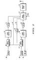
- FIG. 1is a block diagram of a multi-sensor system 101 according to the prior art.
- System 101includes a first sensor 103 and a second sensor 105 .
- Sensor 103may be an accelerometer and sensor 105 may be a photo detector.
- sensor 105is paired with an LED 107 to form a photoplethysmographic sensor.
- Sensor 103is coupled to analog circuitry 109 .
- sensor 105is coupled to analog circuitry 111 .
- Analog circuitry 109 and 111includes various components to process and amplify signals received from sensors 103 and 105 , respectively.
- the outputs of analog circuitry 109 and 111are coupled to analog-to-digital (A/D) converters 113 and 115 , respectively.
- the outputs of A/D converters 113 and 115are coupled to a digital processor 117 .
- Digital processor 117may be a digital signal processor (DSP), a field programmable gate array (FPGA), a complex programmable logic device (CPLD), or the like.
- the output of digital processor 117may be coupled to a wireless module 119 , which may be a radio frequency (RF) or optical device.
- RFradio frequency
- sensors 103 and 105are different, the respective circuitries of analog circuitry 109 and 111 are different as well. Accordingly, the processing times for signals received from sensors 103 and 105 are typically different from each other. Accordingly, while the physical events measured by sensors 103 and 105 are synchronized, the outputs of analog circuitry 109 and 111 , respectively, typically are not. In order for the results yielded by digital processor 117 to be valid, the outputs of A/D converters 113 and 115 must be synchronized.
- FIG. 2is a block diagram of an embodiment of a multi-sensor system according to the present invention.
- System 201includes a first sensor 203 and a second sensor 205 .
- Sensor 205is paired with an LED 207 .
- the output of sensor 203is coupled to an analog multiplexer 209 .
- the output of sensor 205is coupled to an analog multiplexer 211 .
- Analog multiplexers 209 and 211are coupled to a digital processor 213 .
- Digital processor 213is programmed to produce a control signal 215 and a digital marker signal 217 .
- the digital marker signalis a Barker code or sequence.
- a Barker codeis a sequence of N values of +1 and ⁇ 1
- ⁇ ⁇ j1 N - ⁇ ⁇ a j ⁇ a j + ⁇ ⁇ ⁇ 1 , for all integer values of ⁇ , where 1 ⁇ N.
- a Barker code of length thirteenis used in the present invention.
- Digital marker signal 217is coupled to analog multiplexers 209 and 211 through a digital-to-analog (D/A) converter 219 .
- D/Adigital-to-analog
- a marker signalis periodically multiplexed with the analog signals from sensors 203 and 205 .
- the marker signalsprovide a means for synchronizing the signals from sensors 203 and 205 .
- Sensor 203 and/or sensor 205may be antennas.
- Analog multiplexers 209 and 211are coupled to analog circuitry 221 and 223 , respectively.
- the outputs of analog circuitry 221 and 223are coupled to A/D converters 225 and 227 , respectively.
- the outputs of A/D converters 225 and 227are coupled to digital processor 213 .
- the output of digital processor 213may be coupled to a wireless module 229 , so that processed data may be collected remotely.
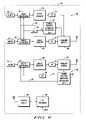
- FIG. 3is a block diagram of an embodiment of a digital processor 213 according to the present invention.
- Digital processor 213may be implemented in a digital signal processor (DSP), a field programmable gate array (FPGA), a complex programmable logic device (CPLD), or the like.
- Digital processor 213includes an input buffer 301 that receives digitized sensor data from A/D converter 225 of FIG. 2 .
- Digital processor 213includes a second input buffer 303 that receives digitized sensor data from A/D converter 227 of FIG. 2 .
- input buffers 301 and 303are first-in-first-out (FIFO) buffers.
- the output of input buffer 301is coupled to a cross-correlator 305 .
- FIFOfirst-in-first-out
- the output of input buffer 303is coupled to a cross-correlator 307 .
- Cross-correlators 305 and 307are also coupled to a Barker sequence generation and control unit 309 .
- Barker sequence generation and control unitsupply multiplexer control signal 215 and Barker sequence 217 to analog multiplexers 209 and 211 of FIG. 2 .
- Cross-correlators 305 and 307perform cross-correlation, which is a mathematical tool used in signal processing to analyze functions or series of values. Cross-correlation is a measure of the similarity of two signals. It may be thought of as a measure of how well an unknown signal matches a known signal. Thus, cross-correlators 305 and 307 match sensor data, into which has been multiplexed a Barker sequence, with the Barker sequence generated directly by Barker sequence generation and control unit 309 .
- Cross-correlators 305 and 307implement the following equation:
- xis the Barker sequence
- yis the data coming into the cross-correlator.
- cross-correlator 305 or 307collects N+1 data samples, where N is the length of the Barker sequence, which in the preferred embodiment is thirteen.
- Each of the N+1 Barker code pointsis multiplied by the corresponding N+1 data sample points read from buffer 301 or 303 .
- cross-correlation valuewhich is the output of cross-correlator 305 and 307 .
- the oldest cross-correlation value data in cross-correlator 305is shifted out to a peak detector 311 .
- the oldest cross-correlation value data in cross-correlator 307is shifted out to a peak detector 313 .
- cross-correlators 305 and 307may be replaced by auto-correlators.
- Autocorrelationis the cross-correlation of a signal with a time shifted version of itself.
- Peak detectors 311 and 313receive cross-correlation value data from cross-correlators 305 and 307 , respectively.
- peak detectors 311 and 313each track the last 2(N+1) correlation values received from cross-correlators 305 and 307 , respectively.
- Peak detectors 311 and 313detect a peak whenever a cross-correlation value exceeds a threshold and a sudden transition occurs. The transition indicates the address at which a Barker code in the sensor data matches the Barker code generated internally by Barker sequence generation and control unit 309 .
- the outputs of peak detectors 311 and 313are coupled to a delta T calculation and address generation unit 315 .
- Delta T calculation and address generation unit 315receives inputs from peak detectors 311 and 313 . When delta T calculation and address generation unit 315 receives an input from peak detector 311 or 313 , it keeps track of the address location where the peak occurred. Delta T calculation and address generation unit 315 then waits for the other peak detector 311 or 313 to detect a peak. After Delta T calculation and address generation unit 315 has received peak signals from both peak detector 311 and 313 , delta T calculation and address generation unit 315 calculates the difference between in the addresses of the peaks. Then, delta T calculation and address generation unit shifts the addresses for the buffers 301 or 303 from which the first peak was detected, thereby synchronizing the outputs of the first 301 and 303 . The synchronized outputs of buffers 301 and 303 are coupled to circuitry 317 for processing synchronized data streams and information extraction. The output of circuitry 317 is enhanced sensor data.
- Analog sensor sub-system 403includes an analog sensor 411 that is coupled to an analog multiplexer 413 .
- Analog multiplexer 413is coupled to analog circuitry 415 which is coupled to a wireless module 417 through an A/D converter 419 .
- Wireless module 417may be an RF or an optical device.
- Wireless module 417that is adapted to send signals to and receive signals from digital processor 409 through a wireless module 421 , which may be an RF or an optical device.
- Wireless module 417transmits and receives using a multiple access technology such as TDMA.
- Wireless module 417is coupled to a Barker sequence generator and control unit 420 .
- wireless module 417receives from wireless module 421 a beacon signal.
- Barker sequence generator and control unit 420generates a Barker sequence 423 and a control signal 425 .
- Barker sequence generator and control unit 420provides Barker sequence 423 , through a D/A converter 424 , and control signal 425 to analog multiplexer 413 .
- Analog sensor sub-system 403operates substantially in the manner described with respect to FIG. 2 except that the digitized output of analog sensor 411 is coupled wirelessly to digital processor 409 rather than by hardwire.
- Analog sensor sub-systems 405 and 407are similar to analog sensor sub-system 403 .
- Analog sensor sub-system 405includes an analog sensor 431 that is coupled to an analog multiplexer 433 .
- Analog multiplexer 433is coupled to analog circuitry 455 which is coupled to a wireless module 437 through an A/D converter 439 .
- Wireless module 437is adapted to send signals to and receive signals from digital processor 409 through wireless module 421 .
- Wireless module 437transmits and receives using a multiple access technology such as TDMA.
- Wireless module 437is coupled to a Barker sequence generator and control unit 440 .
- Wireless module 437receives from wireless module 421 a beacon signal.
- Barker sequence generator and control unit 440generates a Barker sequence 443 and a control signal 445 in response to receipt of the control signal. Barker sequence generator and control unit 440 provides Barker sequence 443 , through a D/A converter 444 , and control signal 445 to analog multiplexer 433 .
- analog sensor sub-system 407includes an analog sensor 451 that is coupled to an analog multiplexer 453 .
- Analog multiplexer 453is coupled to analog circuitry 455 , which is coupled to a wireless module 457 through an A/D converter 459 .
- Wireless module 457is adapted to send signals to and receive signals from digital processor 409 through wireless module 421 . Wireless module 457 transmits and receives using a multiple access technology such as TDMA.
- Wireless module 457is coupled to a Barker sequence generator and control unit 460 .
- Wireless module 457receives from wireless module 421 a beacon signal.
- Barker sequence generator and control unit 460generates a Barker sequence 463 and a control signal 465 in response to receipt of the control signal.
- Barker sequence generator and control unit 440provides Barker sequence 463 , through a D/A converter 464 , and control signal 445 to analog multiplexer 453 . It should be recognized that wireless modules according to embodiments of the present invention may be RF or optical devices.
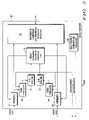
- Digital processor 501may be implemented in a digital signal processor (DSP), a field programmable gate array (FPGA), a complex programmable logic device (CPLD), or the like. Digital processor 501 may be used as an implementation of digital processor 409 of FIG. 4 . Digital processor 501 includes a plurality of input buffers 503 , 505 , and 507 . Buffers 503 , 505 , and 507 receive sensor data either wirelessly, as described with respect to FIG. 4 , and as will be described with reference to FIG. 6 , or wirelessly and by hardwire, as will be described with reference to FIG. 7 .
- DSPdigital signal processor
- FPGAfield programmable gate array
- CPLDcomplex programmable logic device
- Buffers 503 , 505 , and 507are coupled to cross-correlators 509 , 511 , and 513 , respectively.
- Cross-correlators 509 , 511 , and 513are coupled to a Barker sequence generation, control unit, and beacon or synchronization signal generator 523 .
- Barker sequence generation, control unit, and beacon or synchronization signal generator 523generates a multiplexer control signal 525 , a Barker sequence 527 , and a beacon signal 529 .
- Beacon signal 529may be coupled to a wireless module, such as wireless module 421 of FIG. 4 .
- Wireless module 421acts as a beacon to broadcast beacon signal 529 simultaneously to analog sensor sub-systems 403 , 405 , and 407 of FIG. 4 .
- Wireless sensor sub-systemssuch as sub-systems 403 , 405 , and 407 generate Barker sequences and multiplexer control signals in response to receiving the beacon signal.
- Barker sequence 529is coupled to cross-correlators 509 , 511 , and 513 .
- Multiplexer control signal 525 and Barker sequence 527may be coupled by hard wire to analog multiplexers as described for example in connection with FIG. 7 , below.
- Cross-correlators 509 , 511 , and 513are coupled to peak detectors 515 , 517 , and 519 , respectively. Peak detectors 515 , 517 , and 519 are coupled to a delta T calculation and address generation unit 521 . Delta T calculation and address generation unit 521 is coupled to buffers 503 , 505 , and 507 .
- Cross-correlators 503 , 505 , and 507 , peak detectors 515 , 517 , and 519 , and delta T calculation and address generation unit 521operate in the manner describe above with reference to FIG. 3 to synchronize the outputs of buffers 503 , 505 , and 507 .
- the synchronized outputs of buffers 503 , 505 , and 507are coupled to circuitry 525 , which processes the synchronized sensor data streams and extracts information.
- Analog sensor sub-system 603is similar to the analog sensor sub-system of FIG. 2 , in that it includes an analog sensor 611 , coupled to an analog multiplexer 613 , and an analog sensor 615 , coupled to an analog multiplexer 617 .
- Analog multiplexers 613 and 617are coupled to analog circuitry 619 and 621 , respectively, which are coupled to a wireless module 623 through A/D converters 625 and 627 , respectively.
- Wireless module 623that is adapted to send signals to and receive signals from a digital processor 609 through a wireless module 629 .
- Wireless module 623transmits using a multiple access technology such as TDMA.
- Wireless module 623is coupled to a Barker sequence generator and control unit 630 .
- Wireless module 623receives from wireless module 629 a beacon signal.
- Barker sequence generator and control unit 630generates a Barker sequence 631 and a control signal 633 in response to receipt of the beacon signal.
- Barker sequence generator and control unit 630provides Barker sequence 631 , through a D/A converter 635 , and control signal 633 to analog multiplexers 613 and 617 .
- Analog sensor sub-system 603operates substantially in the manner described with respect to FIG. 2 except that the digitized outputs of analog sensors 611 and 615 are coupled wirelessly to digital processor 609 rather than by hardwire.
- Analog sensor sub-system 607includes an analog sensor 641 that is coupled to an analog multiplexer 643 .
- Analog multiplexer 643is coupled to analog circuitry 645 , which is coupled to a wireless module 647 through an A/D converter 649 .
- Wireless module 647that is adapted to send signals to and receive signals from digital processor 609 through wireless module 629 .
- Wireless module 647transmits and receives using a multiple access technology such as TDMA.
- Wireless module 647is coupled to a Barker sequence generator and control unit 650 .
- Wireless module 647receives from wireless module 629 a beacon signal.
- Barker sequence generator and control unit 650generates a Barker sequence 651 and a control signal 653 in response to receipt of the beacon signal.
- Barker sequence generator and control unit 650provides Barker sequence 651 , through a D/A converter 655 , and control signal 653 to analog multiplexer 643 .
- Analog sensor sub-system 607operates substantially in the same manner as analog sensor sub-systems 403 , 405 , and 407 of FIG. 4 .
- FIG. 7illustrates a combination wireless and hardwired embodiment of a system 701 according to the present invention.
- System 701includes a hardwired system 703 , similar to system 201 of FIG. 2 , and a wireless sub-system 705 , similar to systems 403 , 405 , and 407 of FIG. 4 .
- System 703includes an analog sensor 707 , coupled to an analog multiplexer 709 , and an analog sensor 711 , coupled to an analog multiplexer 713 .
- Analog multiplexers 709 and 713are coupled to analog circuitry 715 and 717 , respectively, which are coupled to a digital processor 719 through A/D converters 721 and 723 , respectively.
- Digital processor 719may be implemented in manner described with reference to FIG.
- Barker sequence 731is coupled to analog multiplexers 709 and 713 through D/A converter 735 .
- Digital processor 719is coupled to a wireless module 739 to transmit data extracted by digital processor 719 , as described with reference to FIGS. 3 and 5 .
- Wireless module 739also receives digitized sensor data from, and transmits beacon signals to, system 705 . The timing of the beacon signal may be adjusted to account for delays in transmission to Barker sequence generator 760 through wireless modules 739 and 757 so that the Barker sequences are received simultaneously at analog multiplexers 709 , 713 , and 753 .
- Analog sensor sub-system 705is similar to analog sensor sub-systems 403 , 405 , and 407 of FIG. 4 .
- Analog sensor sub-system 705includes an analog sensor 751 that is coupled to an analog multiplexer 753 .
- Analog multiplexer 753is coupled to analog circuitry 755 , which is coupled to a wireless module 757 through an A/D converter 759 .
- Wireless module 757that is adapted to send data signals to, and receive beacon signals from, digital processor 719 through wireless module 739 .
- Wireless module 757is coupled to a Barker sequence generator and control unit 760 .
- Wireless module 757receives from wireless module 739 beacon signals.
- Barker sequence generator and control unit 760generates a Barker sequence 763 and a control signal 765 in response to receipt of beacon signal. Barker sequence generator and control unit 760 provides Barker sequence 763 , through a D/A converter 764 , and control signal 765 to analog multiplexer 753 .
- embodiments of the invention described hereinmay be comprised of one or more conventional processors and unique stored program instructions that control the one or more processors to implement, in conjunction with certain non-processor circuits, some, most, or all of the functions described herein.
- the non-processor circuitsmay include, but are not limited to, a sensor, a wireless receiver, a wireless transmitter, signal drivers, clock circuits, power source circuits, and user input devices.
- the input datacan come from other remote systems through antennas for example, and the output can be consumed by a sub-system module such as a second circuit within the same electronic system board.
Landscapes
- Engineering & Computer Science (AREA)
- Theoretical Computer Science (AREA)
- Arrangements For Transmission Of Measured Signals (AREA)
Abstract
Description
for all integer values of υ, where 1≦υ≦N.
Preferably, a Barker code of length thirteen is used in the present invention.
where x is the Barker sequence and y is the data coming into the cross-correlator. As the data samples are being read out of
Claims (25)
Priority Applications (2)
| Application Number | Priority Date | Filing Date | Title |
|---|---|---|---|
| US11/755,341US7446694B1 (en) | 2007-05-30 | 2007-05-30 | System for synchronization of multi-sensor data |
| PCT/US2008/064204WO2008150696A1 (en) | 2007-05-30 | 2008-05-20 | System for synchronization of multi-sensor data |
Applications Claiming Priority (1)
| Application Number | Priority Date | Filing Date | Title |
|---|---|---|---|
| US11/755,341US7446694B1 (en) | 2007-05-30 | 2007-05-30 | System for synchronization of multi-sensor data |
Publications (1)
| Publication Number | Publication Date |
|---|---|
| US7446694B1true US7446694B1 (en) | 2008-11-04 |
Family
ID=39916505
Family Applications (1)
| Application Number | Title | Priority Date | Filing Date |
|---|---|---|---|
| US11/755,341ActiveUS7446694B1 (en) | 2007-05-30 | 2007-05-30 | System for synchronization of multi-sensor data |
Country Status (2)
| Country | Link |
|---|---|
| US (1) | US7446694B1 (en) |
| WO (1) | WO2008150696A1 (en) |
Cited By (11)
| Publication number | Priority date | Publication date | Assignee | Title |
|---|---|---|---|---|
| US20100033425A1 (en)* | 2008-08-05 | 2010-02-11 | Judith Shasek | Computer peripheral device interface for simulating mouse, keyboard, or game controller action and method of use |
| US20110148435A1 (en)* | 2009-12-18 | 2011-06-23 | Adam Schwartz | Transcapacitive sensor devices with ohmic seams |
| US20140012509A1 (en)* | 2012-07-06 | 2014-01-09 | Daniel Barber | Methods and systems for synchronization and distribution of multiple physiological and performance measures |
| US8643618B2 (en)* | 2010-09-15 | 2014-02-04 | Uc-Logic Technology Corp. | Electromagnetic-type touch input device, and touch display device incorporating the same |
| US20140147928A1 (en)* | 2012-11-27 | 2014-05-29 | Siemens Healthcare Diagnostics Products Gmbh | Method for ascertaining a transmission value |
| US20140207983A1 (en)* | 2013-01-22 | 2014-07-24 | Apple Inc. | Time-division multiplexed data bus interface |
| US10088942B2 (en) | 2016-03-31 | 2018-10-02 | Synaptics Incorporated | Per-finger force detection using segmented sensor electrodes |
| US10419540B2 (en) | 2015-10-05 | 2019-09-17 | Microsoft Technology Licensing, Llc | Architecture for internet of things |
| WO2020071149A1 (en)* | 2018-10-05 | 2020-04-09 | ソニー株式会社 | Information processing device |
| US11018788B2 (en)* | 2015-12-04 | 2021-05-25 | Infineon Technologies Ag | Robust high speed sensor interface for remote sensors |
| US11022511B2 (en) | 2018-04-18 | 2021-06-01 | Aron Kain | Sensor commonality platform using multi-discipline adaptable sensors for customizable applications |
Citations (14)
| Publication number | Priority date | Publication date | Assignee | Title |
|---|---|---|---|---|
| US4263621A (en)* | 1979-06-21 | 1981-04-21 | The United States Of America As Represented By The Secretary Of The Navy | Charge coupled device signal output summing circuit |
| US4937445A (en)* | 1986-09-24 | 1990-06-26 | Softac Systems Ltd. | Apparatus for determining the distances of points on a surface from a reference axis |
| US5388126A (en) | 1992-12-21 | 1995-02-07 | Rypinski; Chandos A. | Baseband signal processor for a microwave radio receiver |
| US5479240A (en)* | 1994-06-14 | 1995-12-26 | Sindo Ricoh Co., Ltd. | Method for controlling automatic discharge of jammed paper for automatic jam removal |
| US5523788A (en)* | 1994-09-27 | 1996-06-04 | Eastman Kodak Company | Image processor with input buffering to multiple digital signal processors |
| US5734624A (en) | 1996-10-31 | 1998-03-31 | The United States Of America As Represented By The Secretary Of The Navy | Wide-band omni telemetry system |
| US6108462A (en)* | 1994-07-08 | 2000-08-22 | Seiko Epson Corporation | Image processing method and device |
| US6154167A (en)* | 1998-03-20 | 2000-11-28 | Sensors & Software Inc. | Excitation method and ultra-wide bandwidth antenna for ground penetrating radar systems |
| US20020114890A1 (en)* | 2000-09-07 | 2002-08-22 | Posey Robert Giles | Heat seal coating and coated film |
| US6573918B2 (en)* | 2000-08-22 | 2003-06-03 | Ricoh Company, Ltd. | Image forming apparatus having a plurality of image data interfaces |
| US20050066101A1 (en)* | 2003-09-01 | 2005-03-24 | Thomas Fuehrer | Method and device for connecting sensors or actuators to a bus system |
| US7000598B2 (en)* | 2004-05-27 | 2006-02-21 | General Electric Company | Bumpless crankshift position sensing |
| US20060120477A1 (en)* | 2004-12-07 | 2006-06-08 | Adaptix, Inc. | Cooperative MIMO in multicell wireless networks |
| US7196689B2 (en)* | 2003-03-31 | 2007-03-27 | Canon Kabushiki Kaisha | Information device |
Family Cites Families (5)
| Publication number | Priority date | Publication date | Assignee | Title |
|---|---|---|---|---|
| JPS6228850A (en)* | 1985-07-31 | 1987-02-06 | Toshiba Corp | Memory address mapping mechanism |
| JP3061836B2 (en)* | 1990-05-22 | 2000-07-10 | 日本電気株式会社 | Memory device |
| JPH04117530A (en)* | 1990-09-07 | 1992-04-17 | Nec Corp | Single chip microcomputer |
| KR100242462B1 (en)* | 1996-11-07 | 2000-08-01 | 김영환 | A I/O address mapping device using indexing mechanism |
| KR20020020555A (en)* | 2000-09-09 | 2002-03-15 | 구자홍 | stuff bit decision circuit |
- 2007
- 2007-05-30USUS11/755,341patent/US7446694B1/enactiveActive
- 2008
- 2008-05-20WOPCT/US2008/064204patent/WO2008150696A1/enactiveApplication Filing
Patent Citations (17)
| Publication number | Priority date | Publication date | Assignee | Title |
|---|---|---|---|---|
| US4263621A (en)* | 1979-06-21 | 1981-04-21 | The United States Of America As Represented By The Secretary Of The Navy | Charge coupled device signal output summing circuit |
| US4937445A (en)* | 1986-09-24 | 1990-06-26 | Softac Systems Ltd. | Apparatus for determining the distances of points on a surface from a reference axis |
| USRE34749E (en)* | 1986-09-24 | 1994-10-04 | Softac Systems Ltd. | Apparatus for determining the distances of points on a surface from a reference axis |
| US5388126A (en) | 1992-12-21 | 1995-02-07 | Rypinski; Chandos A. | Baseband signal processor for a microwave radio receiver |
| US5479240A (en)* | 1994-06-14 | 1995-12-26 | Sindo Ricoh Co., Ltd. | Method for controlling automatic discharge of jammed paper for automatic jam removal |
| US6108462A (en)* | 1994-07-08 | 2000-08-22 | Seiko Epson Corporation | Image processing method and device |
| US5523788A (en)* | 1994-09-27 | 1996-06-04 | Eastman Kodak Company | Image processor with input buffering to multiple digital signal processors |
| US5734624A (en) | 1996-10-31 | 1998-03-31 | The United States Of America As Represented By The Secretary Of The Navy | Wide-band omni telemetry system |
| US6154167A (en)* | 1998-03-20 | 2000-11-28 | Sensors & Software Inc. | Excitation method and ultra-wide bandwidth antenna for ground penetrating radar systems |
| US6573918B2 (en)* | 2000-08-22 | 2003-06-03 | Ricoh Company, Ltd. | Image forming apparatus having a plurality of image data interfaces |
| US6704035B2 (en)* | 2000-08-22 | 2004-03-09 | Ricoh Company, Ltd. | Image forming apparatus having simple drive timing control |
| US20020114890A1 (en)* | 2000-09-07 | 2002-08-22 | Posey Robert Giles | Heat seal coating and coated film |
| US7196689B2 (en)* | 2003-03-31 | 2007-03-27 | Canon Kabushiki Kaisha | Information device |
| US7298365B2 (en)* | 2003-03-31 | 2007-11-20 | Canon Kabushiki Kaisha | Information device |
| US20050066101A1 (en)* | 2003-09-01 | 2005-03-24 | Thomas Fuehrer | Method and device for connecting sensors or actuators to a bus system |
| US7000598B2 (en)* | 2004-05-27 | 2006-02-21 | General Electric Company | Bumpless crankshift position sensing |
| US20060120477A1 (en)* | 2004-12-07 | 2006-06-08 | Adaptix, Inc. | Cooperative MIMO in multicell wireless networks |
Non-Patent Citations (1)
| Title |
|---|
| Paul Ekas, FPGAs rapidly replacing high-performance DSP capability, Altera Corporation, Feb. 2007. |
Cited By (23)
| Publication number | Priority date | Publication date | Assignee | Title |
|---|---|---|---|---|
| US20100033425A1 (en)* | 2008-08-05 | 2010-02-11 | Judith Shasek | Computer peripheral device interface for simulating mouse, keyboard, or game controller action and method of use |
| US9354264B2 (en) | 2009-12-18 | 2016-05-31 | Synaptics Incorporated | Transcapacitive sensor devices with seams |
| US20110148435A1 (en)* | 2009-12-18 | 2011-06-23 | Adam Schwartz | Transcapacitive sensor devices with ohmic seams |
| US8638107B2 (en) | 2009-12-18 | 2014-01-28 | Synaptics Incorporated | Transcapacitive sensor devices with ohmic seams |
| US9880209B2 (en) | 2009-12-18 | 2018-01-30 | Synaptics Incorporated | Capacitive sensing on large touch screens |
| US9606676B2 (en) | 2009-12-18 | 2017-03-28 | Synaptics Incorporated | Input device |
| US8643618B2 (en)* | 2010-09-15 | 2014-02-04 | Uc-Logic Technology Corp. | Electromagnetic-type touch input device, and touch display device incorporating the same |
| US20140012509A1 (en)* | 2012-07-06 | 2014-01-09 | Daniel Barber | Methods and systems for synchronization and distribution of multiple physiological and performance measures |
| US9664670B2 (en)* | 2012-11-27 | 2017-05-30 | Siemens Healthcare Diagnostics Products Gmbh | Method for ascertaining a transmission value |
| CN103837690A (en)* | 2012-11-27 | 2014-06-04 | 西门子医学诊断产品有限责任公司 | Method for ascertaining a transmission value |
| US20140147928A1 (en)* | 2012-11-27 | 2014-05-29 | Siemens Healthcare Diagnostics Products Gmbh | Method for ascertaining a transmission value |
| CN103837690B (en)* | 2012-11-27 | 2018-09-18 | 西门子医学诊断产品有限责任公司 | Method for determining transmission value |
| US10146732B2 (en)* | 2013-01-22 | 2018-12-04 | Apple Inc. | Time-division multiplexed data bus interface |
| US20140207983A1 (en)* | 2013-01-22 | 2014-07-24 | Apple Inc. | Time-division multiplexed data bus interface |
| US10419540B2 (en) | 2015-10-05 | 2019-09-17 | Microsoft Technology Licensing, Llc | Architecture for internet of things |
| US11018788B2 (en)* | 2015-12-04 | 2021-05-25 | Infineon Technologies Ag | Robust high speed sensor interface for remote sensors |
| US11728916B2 (en) | 2015-12-04 | 2023-08-15 | Infineon Technologies Ag | Robust high speed sensor interface for remote sensors |
| US10088942B2 (en) | 2016-03-31 | 2018-10-02 | Synaptics Incorporated | Per-finger force detection using segmented sensor electrodes |
| US11022511B2 (en) | 2018-04-18 | 2021-06-01 | Aron Kain | Sensor commonality platform using multi-discipline adaptable sensors for customizable applications |
| WO2020071149A1 (en)* | 2018-10-05 | 2020-04-09 | ソニー株式会社 | Information processing device |
| JPWO2020071149A1 (en)* | 2018-10-05 | 2021-10-07 | ソニーグループ株式会社 | Information processing device |
| JP7367690B2 (en) | 2018-10-05 | 2023-10-24 | ソニーグループ株式会社 | information processing equipment |
| US12142249B2 (en) | 2018-10-05 | 2024-11-12 | Sony Group Corporation | Information processing apparatus |
Also Published As
| Publication number | Publication date |
|---|---|
| WO2008150696A1 (en) | 2008-12-11 |
Similar Documents
| Publication | Publication Date | Title |
|---|---|---|
| US7446694B1 (en) | System for synchronization of multi-sensor data | |
| US7558157B1 (en) | Sensor synchronization using embedded atomic clocks | |
| EP3978949A3 (en) | System and method for wireless motion monitoring | |
| US6942621B2 (en) | Method and apparatus for detecting weak physiological signals | |
| CN101371569B (en) | Detection of the presence of television signals embedded in noise using cyclostationary toolbox | |
| US7880721B2 (en) | Wave receiving device and method of determining wave reception | |
| US7777676B2 (en) | Method of lightning location using time difference of arrival technology with auto correlation | |
| US7195596B2 (en) | Pulse wave detecting apparatus and fourier transform process apparatus | |
| GB0227503D0 (en) | Devices,systems and methods for obtaining timing information and ranging | |
| KR970705262A (en) | METHOD AND DEVICE FOR SYNCHRONIZATION OF TRANSMITTER AND RECEIVER IN A DIGITAL SYSTEM - | |
| US20120274793A1 (en) | System and method for synchronizing video and sensor signals | |
| JP2010230467A (en) | Positioning system, positioning device, positioning method, and program | |
| KR100658223B1 (en) | High precision time synchronization device and method in real time location tracking system | |
| KR20180050947A (en) | Representative waveform providing apparatus and method | |
| KR0150700B1 (en) | Point type wireless controller using infrared rays | |
| WO2020157039A3 (en) | Device for processing a signal of a locating system, and method for simulating and for locating an object | |
| KR20150044311A (en) | Method and apparatus for generating of synchronization signal using electrocardiogram signal | |
| US20060183485A1 (en) | Location system and wireless base station | |
| US7460012B2 (en) | Method and system for synchronizing geographically distributed RF sensors using a pair of RF triggering devices | |
| EP4287647A1 (en) | Information processing apparatus, information processing method, and program | |
| JP2016080398A (en) | Biological-information detection rader system | |
| US8941516B2 (en) | Signal processing apparatus and signal processing method thereof | |
| EP1118875A3 (en) | Ultrasound diagnostic apparatus | |
| JP2000266626A (en) | Apparatus for simultaneous multipoint measurement | |
| WO2025009475A1 (en) | Measurement system, measurement device, and analysis device |
Legal Events
| Date | Code | Title | Description |
|---|---|---|---|
| AS | Assignment | Owner name:MOTOROLA, INC., ILLINOIS Free format text:ASSIGNMENT OF ASSIGNORS INTEREST;ASSIGNORS:AHMED, MOHAMED I.;ISHTIAQ, FAISAL;MOHAMED, MAGDI A.;AND OTHERS;REEL/FRAME:019356/0782;SIGNING DATES FROM 20070523 TO 20070525 | |
| STCF | Information on status: patent grant | Free format text:PATENTED CASE | |
| AS | Assignment | Owner name:MOTOROLA SOLUTIONS, INC., ILLINOIS Free format text:CHANGE OF NAME;ASSIGNOR:MOTOROLA, INC;REEL/FRAME:026081/0001 Effective date:20110104 | |
| FPAY | Fee payment | Year of fee payment:4 | |
| FPAY | Fee payment | Year of fee payment:8 | |
| AS | Assignment | Owner name:ARRIS ENTERPRISES LLC, PENNSYLVANIA Free format text:ASSIGNMENT OF ASSIGNORS INTEREST;ASSIGNOR:MOTOROLA SOLUTIONS, INC.;REEL/FRAME:044806/0900 Effective date:20170830 | |
| AS | Assignment | Owner name:WILMINGTON TRUST, NATIONAL ASSOCIATION, AS COLLATE Free format text:PATENT SECURITY AGREEMENT;ASSIGNOR:ARRIS ENTERPRISES LLC;REEL/FRAME:049820/0495 Effective date:20190404 Owner name:JPMORGAN CHASE BANK, N.A., NEW YORK Free format text:TERM LOAN SECURITY AGREEMENT;ASSIGNORS:COMMSCOPE, INC. OF NORTH CAROLINA;COMMSCOPE TECHNOLOGIES LLC;ARRIS ENTERPRISES LLC;AND OTHERS;REEL/FRAME:049905/0504 Effective date:20190404 Owner name:JPMORGAN CHASE BANK, N.A., NEW YORK Free format text:ABL SECURITY AGREEMENT;ASSIGNORS:COMMSCOPE, INC. OF NORTH CAROLINA;COMMSCOPE TECHNOLOGIES LLC;ARRIS ENTERPRISES LLC;AND OTHERS;REEL/FRAME:049892/0396 Effective date:20190404 Owner name:WILMINGTON TRUST, NATIONAL ASSOCIATION, AS COLLATERAL AGENT, CONNECTICUT Free format text:PATENT SECURITY AGREEMENT;ASSIGNOR:ARRIS ENTERPRISES LLC;REEL/FRAME:049820/0495 Effective date:20190404 | |
| MAFP | Maintenance fee payment | Free format text:PAYMENT OF MAINTENANCE FEE, 12TH YEAR, LARGE ENTITY (ORIGINAL EVENT CODE: M1553); ENTITY STATUS OF PATENT OWNER: LARGE ENTITY Year of fee payment:12 | |
| AS | Assignment | Owner name:WILMINGTON TRUST, DELAWARE Free format text:SECURITY INTEREST;ASSIGNORS:ARRIS SOLUTIONS, INC.;ARRIS ENTERPRISES LLC;COMMSCOPE TECHNOLOGIES LLC;AND OTHERS;REEL/FRAME:060752/0001 Effective date:20211115 | |
| AS | Assignment | Owner name:APOLLO ADMINISTRATIVE AGENCY LLC, NEW YORK Free format text:SECURITY INTEREST;ASSIGNORS:ARRIS ENTERPRISES LLC;COMMSCOPE TECHNOLOGIES LLC;COMMSCOPE INC., OF NORTH CAROLINA;AND OTHERS;REEL/FRAME:069889/0114 Effective date:20241217 | |
| AS | Assignment | Owner name:RUCKUS WIRELESS, LLC (F/K/A RUCKUS WIRELESS, INC.), NORTH CAROLINA Free format text:RELEASE OF SECURITY INTEREST AT REEL/FRAME 049905/0504;ASSIGNOR:JPMORGAN CHASE BANK, N.A., AS COLLATERAL AGENT;REEL/FRAME:071477/0255 Effective date:20241217 Owner name:COMMSCOPE TECHNOLOGIES LLC, NORTH CAROLINA Free format text:RELEASE OF SECURITY INTEREST AT REEL/FRAME 049905/0504;ASSIGNOR:JPMORGAN CHASE BANK, N.A., AS COLLATERAL AGENT;REEL/FRAME:071477/0255 Effective date:20241217 Owner name:COMMSCOPE, INC. OF NORTH CAROLINA, NORTH CAROLINA Free format text:RELEASE OF SECURITY INTEREST AT REEL/FRAME 049905/0504;ASSIGNOR:JPMORGAN CHASE BANK, N.A., AS COLLATERAL AGENT;REEL/FRAME:071477/0255 Effective date:20241217 Owner name:ARRIS SOLUTIONS, INC., NORTH CAROLINA Free format text:RELEASE OF SECURITY INTEREST AT REEL/FRAME 049905/0504;ASSIGNOR:JPMORGAN CHASE BANK, N.A., AS COLLATERAL AGENT;REEL/FRAME:071477/0255 Effective date:20241217 Owner name:ARRIS TECHNOLOGY, INC., NORTH CAROLINA Free format text:RELEASE OF SECURITY INTEREST AT REEL/FRAME 049905/0504;ASSIGNOR:JPMORGAN CHASE BANK, N.A., AS COLLATERAL AGENT;REEL/FRAME:071477/0255 Effective date:20241217 Owner name:ARRIS ENTERPRISES LLC (F/K/A ARRIS ENTERPRISES, INC.), NORTH CAROLINA Free format text:RELEASE OF SECURITY INTEREST AT REEL/FRAME 049905/0504;ASSIGNOR:JPMORGAN CHASE BANK, N.A., AS COLLATERAL AGENT;REEL/FRAME:071477/0255 Effective date:20241217 |