US7446410B2 - Circuit module with thermal casing systems - Google Patents
Circuit module with thermal casing systemsDownload PDFInfo
- Publication number
- US7446410B2 US7446410B2US11/283,355US28335505AUS7446410B2US 7446410 B2US7446410 B2US 7446410B2US 28335505 AUS28335505 AUS 28335505AUS 7446410 B2US7446410 B2US 7446410B2
- Authority
- US
- United States
- Prior art keywords
- thermal
- substrate
- circuit
- circuit module
- flex
- Prior art date
- Legal status (The legal status is an assumption and is not a legal conclusion. Google has not performed a legal analysis and makes no representation as to the accuracy of the status listed.)
- Expired - Lifetime, expires
Links
Images


Classifications
- H—ELECTRICITY
- H05—ELECTRIC TECHNIQUES NOT OTHERWISE PROVIDED FOR
- H05K—PRINTED CIRCUITS; CASINGS OR CONSTRUCTIONAL DETAILS OF ELECTRIC APPARATUS; MANUFACTURE OF ASSEMBLAGES OF ELECTRICAL COMPONENTS
- H05K1/00—Printed circuits
- H05K1/18—Printed circuits structurally associated with non-printed electric components
- H05K1/189—Printed circuits structurally associated with non-printed electric components characterised by the use of a flexible or folded printed circuit
- H—ELECTRICITY
- H05—ELECTRIC TECHNIQUES NOT OTHERWISE PROVIDED FOR
- H05K—PRINTED CIRCUITS; CASINGS OR CONSTRUCTIONAL DETAILS OF ELECTRIC APPARATUS; MANUFACTURE OF ASSEMBLAGES OF ELECTRICAL COMPONENTS
- H05K1/00—Printed circuits
- H05K1/02—Details
- H05K1/0201—Thermal arrangements, e.g. for cooling, heating or preventing overheating
- H05K1/0203—Cooling of mounted components
- H—ELECTRICITY
- H05—ELECTRIC TECHNIQUES NOT OTHERWISE PROVIDED FOR
- H05K—PRINTED CIRCUITS; CASINGS OR CONSTRUCTIONAL DETAILS OF ELECTRIC APPARATUS; MANUFACTURE OF ASSEMBLAGES OF ELECTRICAL COMPONENTS
- H05K2201/00—Indexing scheme relating to printed circuits covered by H05K1/00
- H05K2201/05—Flexible printed circuits [FPCs]
- H05K2201/056—Folded around rigid support or component
- H—ELECTRICITY
- H05—ELECTRIC TECHNIQUES NOT OTHERWISE PROVIDED FOR
- H05K—PRINTED CIRCUITS; CASINGS OR CONSTRUCTIONAL DETAILS OF ELECTRIC APPARATUS; MANUFACTURE OF ASSEMBLAGES OF ELECTRICAL COMPONENTS
- H05K2201/00—Indexing scheme relating to printed circuits covered by H05K1/00
- H05K2201/09—Shape and layout
- H05K2201/09209—Shape and layout details of conductors
- H05K2201/09372—Pads and lands
- H05K2201/09445—Pads for connections not located at the edge of the PCB, e.g. for flexible circuits
- H—ELECTRICITY
- H05—ELECTRIC TECHNIQUES NOT OTHERWISE PROVIDED FOR
- H05K—PRINTED CIRCUITS; CASINGS OR CONSTRUCTIONAL DETAILS OF ELECTRIC APPARATUS; MANUFACTURE OF ASSEMBLAGES OF ELECTRICAL COMPONENTS
- H05K2201/00—Indexing scheme relating to printed circuits covered by H05K1/00
- H05K2201/10—Details of components or other objects attached to or integrated in a printed circuit board
- H05K2201/10007—Types of components
- H05K2201/10159—Memory
- H—ELECTRICITY
- H05—ELECTRIC TECHNIQUES NOT OTHERWISE PROVIDED FOR
- H05K—PRINTED CIRCUITS; CASINGS OR CONSTRUCTIONAL DETAILS OF ELECTRIC APPARATUS; MANUFACTURE OF ASSEMBLAGES OF ELECTRICAL COMPONENTS
- H05K2201/00—Indexing scheme relating to printed circuits covered by H05K1/00
- H05K2201/10—Details of components or other objects attached to or integrated in a printed circuit board
- H05K2201/10431—Details of mounted components
- H05K2201/1056—Metal over component, i.e. metal plate over component mounted on or embedded in PCB
- H—ELECTRICITY
- H05—ELECTRIC TECHNIQUES NOT OTHERWISE PROVIDED FOR
- H05K—PRINTED CIRCUITS; CASINGS OR CONSTRUCTIONAL DETAILS OF ELECTRIC APPARATUS; MANUFACTURE OF ASSEMBLAGES OF ELECTRICAL COMPONENTS
- H05K2201/00—Indexing scheme relating to printed circuits covered by H05K1/00
- H05K2201/10—Details of components or other objects attached to or integrated in a printed circuit board
- H05K2201/10613—Details of electrical connections of non-printed components, e.g. special leads
- H05K2201/10621—Components characterised by their electrical contacts
- H05K2201/10734—Ball grid array [BGA]; Bump grid array
- H—ELECTRICITY
- H05—ELECTRIC TECHNIQUES NOT OTHERWISE PROVIDED FOR
- H05K—PRINTED CIRCUITS; CASINGS OR CONSTRUCTIONAL DETAILS OF ELECTRIC APPARATUS; MANUFACTURE OF ASSEMBLAGES OF ELECTRICAL COMPONENTS
- H05K2203/00—Indexing scheme relating to apparatus or processes for manufacturing printed circuits covered by H05K3/00
- H05K2203/15—Position of the PCB during processing
- H05K2203/1572—Processing both sides of a PCB by the same process; Providing a similar arrangement of components on both sides; Making interlayer connections from two sides
- H—ELECTRICITY
- H05—ELECTRIC TECHNIQUES NOT OTHERWISE PROVIDED FOR
- H05K—PRINTED CIRCUITS; CASINGS OR CONSTRUCTIONAL DETAILS OF ELECTRIC APPARATUS; MANUFACTURE OF ASSEMBLAGES OF ELECTRICAL COMPONENTS
- H05K3/00—Apparatus or processes for manufacturing printed circuits
- H05K3/0058—Laminating printed circuit boards onto other substrates, e.g. metallic substrates
- H05K3/0061—Laminating printed circuit boards onto other substrates, e.g. metallic substrates onto a metallic substrate, e.g. a heat sink
Definitions
- the present inventionrelates to systems and methods for creating high density circuit modules and, in particular, to systems and methods for creating such modules with features directed to reducing thermal loading.
- DIMMDual In-line Memory Module
- PCBprinted circuit board
- the DIMMis typically mounted in the host computer system by inserting a contact-bearing edge of the DIMM into a card edge connector.
- systems that employ DIMMsprovide limited profile space for such devices and conventional DIMM-based solutions have typically provided only a moderate amount of memory expansion.
- fewer devices per channelcan be reliably addressed with a DIMM-based solution.
- 288 ICs or devices per channelmay be addressed using the SDRAM-100 bus protocol with an unbuffered DIMM.
- DDR-200 bus protocolapproximately 144 devices may be addressed per channel.
- DDR2-400 bus protocolonly 72 devices per channel may be addressed.
- FB-DIMMfully-buffered DIMM
- That buffering functionis provided by what is typically identified as the Advanced Memory Buffer or AMB.
- the FB-DIMMnot only has capacity increased, pin count has declined to approximately 69 signal pins from the approximately 240 pins previously required.
- the FB-DIMM circuit solutionis expected to offer practical motherboard memory capacities of up to about 192 gigabytes with six channels and eight DIMMs per channel and two ranks per DIMM using one gigabyte DRAMs. This solution should also be adaptable to next generation technologies and should exhibit significant downward compatibility.
- MDPMultiple die packages
- This schemeincreases the capacity of the memory devices on the DIMM by including multiple semiconductor die in a single device package.
- the additional heat generated by the multiple dietypically requires, however, additional cooling capabilities to operate at maximum operating speed.
- the MDP schememay exhibit increased costs because of increased yield loss from packaging together multiple die that are not fully pre-tested.
- Stacked packagesare yet another way to increase module capacity. Capacity is increased by stacking packaged integrated circuits to create a high-density circuit module for mounting on the larger circuit board. In some techniques, flexible conductors are used to selectively interconnect packaged integrated circuits. Staktek Group L.P. has developed numerous systems for aggregating CSP (chipscale packaged) devices in space saving topologies. The increased component height of some stacking techniques may, however, alter system requirements such as, for example, required cooling airflow or the minimum spacing around a circuit board on its host system.
- the known methods for improved memory module performance or enlarged capacityraise thermal management issues.
- the primary thermal pathis through the balls of the package into the core of a multilayer DIMM that has less than desirable thermal characteristics.
- AMBadvanced memory buffer
- FB-DIMMFB-DIMM
- a significant amount of heatis generated. Consequently, the already marginal thermal shedding attributes of DIMM circuit modules is exacerbated in a typical FB-DIMM by the localized generation of heat by the AMB.
- Flexible circuitryis populated with integrated circuitry (ICs) disposed along one or both major sides of the flexible circuitry. Contacts are distributed along the flexible circuitry to provide connection between the module and an application environment.
- the populated flexible circuitryis supported by a rigid substrate, about which it is disposed in preferred embodiments, thus placing the integrated circuitry on one or both sides of the substrate with one or more layers of integrated circuitry on one or both sides of the substrate.
- the substrateis preferably devised from thermally-conductive materials and one or more thermal spreaders are disposed in thermal contact or connection with at least some of the constituent integrated circuitry of the module.
- the modulemay include a high thermal conductivity thermal sink or area that is disposed proximal to higher thermal energy IC devices.
- extensions from the substrate bodyencourage reduced thermal variations amongst the ICs of the module while providing an enlarged surface for shedding thermal energy from the module.
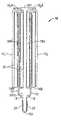
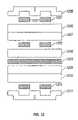
- FIG. 1depicts a perspective view of a module devised in accordance with a preferred embodiment of the present invention.
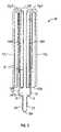
- FIG. 2is an enlarged view of the area marked “A” in FIG. 1 .
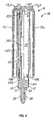
- FIG. 3is a cross-sectional depiction of a preferred embodiment taken along a perspective line that corresponds to line B-B of FIG. 1 .
- FIG. 4is a cross-sectional view of a preferred embodiment taken along a perspective line that corresponds to line C-C of FIG. 1 .
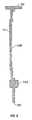
- FIG. 5is a depiction of a substrate employed in a preferred embodiment of the present invention.
- FIG. 6illustrates a substrate employed with an alternative embodiment of the present invention in which an area of the substrate is deformed to provide an indentation.
- FIG. 7depicts one side of a flex circuit employed in a preferred embodiment of the present invention.
- FIG. 8depicts another side of the flex circuit depicted in FIG. 7 .
- FIG. 9is a view of a preferred embodiment before thermal spreaders devised in accordance with a preferred embodiment of the present invention are included in the module.
- a cutaway area Dis provided to enhance illustration of certain features.
- FIG. 10is an enlarged depiction of the area identified with “D” in FIG. 9 .
- FIG. 11is a cross-sectional depiction of the area near an end of a substrate as employed in a preferred embodiment of the present invention.
- FIG. 12is an exploded cross-sectional view of a flex circuit employed in a preferred embodiment of the present invention.
- FIG. 13is a cross-sectional view of another preferred embodiment devised in accordance with the invention.
- FIG. 14is an enlarged perspective view of the preferred embodiment of FIG. 13 devised in accordance with the present invention.
- FIG. 15is another cross-sectional view of another preferred embodiment devised in accordance with the invention.
- FIG. 16is an enlarged perspective view of the preferred embodiment of FIG. 15 devised in accordance with the present invention.
- FIG. 17is another cross-sectional view of another preferred embodiment devised in accordance with the invention.
- FIGS. 1 and 2depict a module 10 devised in accordance with a preferred embodiment of the present invention.
- the depictionsillustrate module 10 having substrate 14 about which is disposed flex circuit 12 populated with ICs 18 which are, in a preferred embodiment, integrated circuitry in CSP packages. Some alternative embodiments will have separate flex circuit on each side of substrate 14 .
- Substrate 14is shown with an optional extension 16 T which, in this embodiment, is integral with the body 14 B of substrate 14 .
- Optional extension 16 Tmay be devised in a variety of configurations and need not extend laterally from the main axis of substrate 14 in both directions.
- extension 16 Tmay extend from substrate 14 in only one direction and need not project perpendicular from the body 14 B of substrate 14 .
- substrate 14is comprised of thermally conductive material.
- Metallic materialsare preferred choices. For example, aluminum like many other metallic materials, is thermally conductive and may be readily manipulated for configuration as substrate 14 .
- Materials such as FR4may be employed, but if non-metallic materials are employed, other non-metallic materials that are thermally conductive are preferred over FR4.
- Carbon-based materials and certain plastics, for example,are known to readily conduct thermal energy and, as alternatives to metallic materials, such materials may be employed to advantage in preferred embodiments in accordance with the present invention where metallic materials are not available or wanted.
- thermal spreaders 13 1 and 13 2are thermally connected to ICs 18 and substrate 14 .
- Thermal spreaders 13 1 and 13 2are comprised of thermally conductive material with higher conductivity metallic materials being preferred. Aluminum is a preferred choice for thermal spreaders in this embodiment due to its amenability to fabrication and relatively high thermal conductivity. Those of skill will recognize, however, that use of copper and copper alloys for thermal spreaders 13 1 and 13 2 will typically provide even greater thermal benefits although at typically a higher cost.
- Thermal spreaders 13 1 and 13 2are preferably thermally connected to ICs 18 (or other ICs where accessible) with thermal adhesive.
- ICs 18are partially shown in FIG. 2 with portions of profiles that represent just some of the many profiles that may be exhibited by ICs 18 .
- ICs 18 on flexible circuit 12are, in this preferred embodiment, CSP packaged memory devices of small scale.
- chip-scale or “CSP”shall refer to integrated circuitry of any function with an array package providing connection to one or more die through contacts (often embodied as “bumps” or “balls” for example) distributed across a major surface of the package or die.
- CSPdoes not refer to leaded devices that provide connection to an integrated circuit within the package through leads emergent from at least one side of the periphery of the package such as, for example, a TSOP.
- Embodiments of the present inventionmay be employed with leaded or CSP devices or other devices in both packaged and unpackaged forms but where the term CSP is used, the above definition for CSP should be adopted. Consequently, although CSP excludes leaded devices, references to CSP are to be broadly construed to include the large variety of array devices (and not to be limited to memory only) and whether die-sized or other size such as BGA and micro BGA as well as flip-chip. As those of skill will understand after appreciating this disclosure, some embodiments of the present invention may be devised to employ stacks of ICs each disposed where an IC 18 is indicated in the exemplar Figs.
- Multiple integrated circuit diemay be included in a package depicted as a single IC 18 . While in this embodiment memory ICs are used to provide a memory expansion board or module, various embodiments may include a variety of integrated circuits and other components and may be directed principally to functions other than or in addition to memory. Such variety may include processors—whether general purpose or function specific such as graphics, FPGA's, RF transceiver circuitry, and digital logic as a list of non-limiting examples, while primary module functions may include, as a non limiting list of examples, memory, graphics, communications, and computing to name just a few examples.
- modules in accordance with a preferred embodimentwill exhibit plural CSPs of a first type, such as memory CSPs, for example, and will have at least one CSP of a second type, such as a microprocessor, graphics processor or buffer or, more particularly, an AMB, for example.
- Other moduleswill exhibit ICs of only a first type such as memory CSPs, for example, while other modules may exhibit many types of ICs such as, for example, memory ICs, logic ICs, and one or more buffer ICs.
- FIG. 3is a cross-sectional depiction of an exemplar module 10 taken along a line corresponding to B-B of FIG. 1 .
- ICs 18are shown as being thermally connected to thermal spreaders 13 1 and 13 2 .
- the thermal connection between thermal spreaders 13 1 and 13 2 and ICs 18can be effectuated by direct contact or through an intermediate substance, particularly one that encourages thermal conduction.
- An example of such a substanceis indicated in FIG. 3 with reference 30 representative of a thermal adhesive.
- Thermal adhesiveis also preferred between ICs 18 and substrate 14 as shown.
- Optional flex support 14 FSsupports flex circuit 12 in its transition from end 16 A of substrate 14 toward the ICs.
- FIG. 3may be also representative of a cross-sectional view through an exemplar module 10 along a line corresponding to C-C of FIG. 1 as well as line B-B in those instances where module 10 consists primarily of ICs 18 along its entire length.
- a typical memory module 10comprising constituent CSP ICs 18 along its length may have a cross-sectional aspect that may be represented by the depiction of FIG. 3 when flex circuit 12 is populated on both sides while thermal spreaders 13 1 and 13 2 are disposed adjacent and thermally connected to ICs 18 B which are populated on side 8 of flex circuit 12 as further shown in FIG. 7 .
- Reference to FIG. 7illustrates that the ICs 18 B represented as being thermally connected to thermal spreaders 13 1 and 13 2 are disposed in two ranks separated by contacts 20 .
- optional substrate extension 16 Tenables a thermal conduction path for thermal energy to flow from inner ICs 18 A (shown proximal to substrate 14 in FIG. 3 ) into thermal spreaders 13 1 and 13 2 through the thermal connection shown extant between substrate 14 and thermal spreaders 13 1 and 13 2 effectuated by substrate extension 16 T in thermal connection with thermal spreader extensions 13 1 A and 13 2 A, respectively.
- FIG. 4is a cross-sectional view of an exemplar module 10 that employs a larger IC 19 such as an AMB 19 with the view of FIG. 4 being taken along a line that corresponds to C-C of FIG. 1 .
- FIG. 4shows a substrate 14 with a window 250 through which an optional thermal sink 14 TS is accessible.
- Thermal sink 14 TSis comprised, in this preferred embodiment, from metallic material of high thermal conductivity such as, for example, copper or copper alloy and has, in this preferred embodiment, a central portion 14 TC that is a copper field substantially larger than and preferably in thermal contact with IC 19 which, in this preferred embodiment, is an AMB.
- AMB die 19 Dis in contact with area 14 TC of thermal sink 14 TS either directly, or through thermally conductive adhesive or a thermally conductive gasket material, for example. Thermal contact with a part of circuit 19 should be considered thermal contact with circuit 19 .
- central portion 14 TC of thermal sink 14 TSis raised above the periphery of thermal sink 14 TS and additionally provides an indentation into which may be introduced at least a portion of AMB circuit 19 such as, for example, AMB die 19 D, to assist in realization of a low profile for module 10 .
- thermal sink 14 TSnor an indentation are required, however, to practice the invention.
- thermal sink 14 TSis disposed over a window 250 through substrate 14 .
- AMB circuit 19which is mounted on the “inside” of flex circuit 12 , is disposed, at least in part, into window 250 from the “back” side of substrate 14 to realize thermal contact with thermal sink 14 TS to provide a conduit to reduce thermal energy loading of AMB circuit 19 .
- Thermal sink 14 TSneed not cover the entirety of window 250 .
- thermal sink 14 TSmay merely be across the window 250 or thermal sink 14 TS may be set into window 250 instead of over or across the opening of window 250 .
- Thermal sink 14 TSis typically a separate piece of metal from substrate 14 but, after appreciating this specification, those of skill will recognize that, in alternative instances, thermal sink 14 TS may be integral with substrate 14 or a particular portion of substrate 14 may be constructed to be a thermal sink 14 TS in accordance with the teachings herein.
- substrate 14may be comprised of aluminum, while a thermal sink area 14 TS of substrate 14 may be comprised of copper yet substrate 14 and thermal sink 14 TS are of a single piece.
- thermal sink 14 TSshould be considered to be an area or element integral with or attached to a substrate 14 and the material from which that thermal sink is composed exhibits greater thermal conductivity than the material of the substrate.
- substrate 14may be aluminum while thermal sink 14 TS is comprised of copper.
- Substrate 14has first and second lateral sides identified as S 1 and S 2 . Flex 12 is wrapped about perimeter edge 16 A of substrate 14 . Some alternative embodiments may employ individual flex circuits on each side of substrate 14 . As will be further shown, AMB circuit 19 is mounted on inner side 9 of flex circuit 12 . When flex circuit 12 is disposed about substrate 14 , AMB circuit 19 is introduced, at least in part, into window 250 with AMB die 19 D being disposed, preferably, in thermal contact with thermal sink 14 TS of substrate 14 . That thermal contact is preferably through thermally conductive adhesive 30 but, in an alternative embodiment, another preferred construction may place AMB die 19 D in direct physical contact with thermal sink 14 TS to realize the thermal contact or connection between AMB circuit 19 and thermal sink 14 TS. Other thermal conduction enhancing materials may also be used in place of, or addition to thermal adhesive 30 such as for example, thermal grease or a thermal gasket.
- thermal spreaders 13 1 and 13 2exhibit optional thermal spreader extensions 13 1 A and 13 2 A which, as previously described, provide a thermal conduction path for thermal energy from the inner ICs 18 A. They also, as shown, in cooperation with extension 16 T, form a thermally conductive enclosure 11 over module 10 . Thermal spreader extensions are not required as a part of thermal spreaders 13 1 and 13 2 , but where employed as those of skill will recognize, they may provide thermal or structural advantages.
- thermal sink 14 TSin this depiction may be copper, for example, while the main body of substrate 14 may be comprised of aluminum, to name just one example.
- Flex support 14 FSis also shown in FIG. 5 and is typically comprised of the same material as substrate 14 .
- FIG. 6illustrates a substrate employed with another alternative embodiment of the present invention in which an area of the substrate is deformed to provide an indentation but no thermal sink 14 TS is employed.
- embodiments that employ substrates such as that depicted in FIG. 6will not have a thermal sink, but may rely on thermal connection or contact between substrate 14 and IC 19 to dissipate heat generated by IC 19 where IC 19 has been mounted on inner side 9 of flex circuit 12 as shown later.
- indentation 14 INis not required but provides low profile advantages.
- an exemplar embodiment that employed a substrate such as that shown in FIG. 6 and does not exhibit a thermal sink 14 TSwould look very much like the embodiment shown in FIG. 4 except that the structure labeled 14 TS would not be separate from substrate 14 and would be a part of substrate 14 and composed from the same material. Further, no window 250 would be present since no opening in substrate 14 would be needed. IC 19 would preferably be in thermal contact with substrate 14 .
- thermal sink 14 TSshould be accessible through window 250 from the “other” side of substrate 14 .
- AMB circuit 19 or other high heat IC 19 and, in particular, AMB die 19 Dmay be disposed in or across or over window 250 and preferably, will be introduced into an indentation of thermal sink 14 TS and disposed in thermal contact with thermal sink 14 TS and, more preferably, with the central core 14 TC of thermal sink 14 TS (where a central core has been optionally included in thermal sink 14 TS) either with direct contact or through thermal adhesives or glues.
- Other embodimentsmay include additional windows where other high heat circuits are employed on module 10 .
- Still other embodimentsmay insert some or all of ICs 18 into cutout areas in substrate 14 as described in detail in U.S.
- thermal sink 14 TScovers window 250 on one side of substrate 14 while AMB circuit 19 is disposed, at least in part, into window 250 to realize contact between thermal sink 14 TS and AMB circuit 19 and particularly AMB die 19 D either directly or as mediated through a thermally-conductive adhesive or glue.
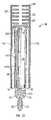
- FIG. 7depicts a first side 8 of flex circuit 12 (“flex”, “flex circuitry”, “flexible circuit”) used in constructing a module according to an embodiment of the present invention.
- Flex circuit 12is preferably made from one or more conductive layers supported by one or more flexible substrate layers as further described with reference to later FIG. 12 .
- the construction of flex circuitryis known in the art.
- the entirety of the flex circuit 12may be flexible or, as those of skill in the art will recognize, the flexible circuit structure 12 may be made flexible in certain areas to allow conformability to required shapes or bends, and rigid in other areas to provide rigid and planar mounting surfaces.
- Preferred flex circuit 12has openings 17 for use in aligning flex circuit 12 to substrate 14 during assembly.
- FIG. 7shows flex circuit 12 as having first and second fields or ranks of ICs 18 with contacts 20 being disposed between said ranks or fields of ICs 18 .
- contacts 20may appear on one or both sides of module 10 depending on the mechanical contact interface particulars of the application.
- Other embodimentsmay employ flex circuitry that exhibits contacts closer to an edge of the flex circuit.
- Flex circuit 12may also referenced by its perimeter edges, two of which are typically long (PE long1 and PE long 2 ) and two of which are typically shorter (PE short1 and PE short2 ) although flex circuit 12 may come in a variety of shapes including square.
- Contact arrayssuch as array 11 A are disposed beneath ICs 18 and IC 19 , where employed, and are comprised of array contacts 11 C.
- An exemplar contact array 11 Ais shown as is exemplar IC 18 to be mounted at contact array 11 A as depicted.
- a first rank, group or plurality of ICs 18is shown on side 8 of flex circuit 12 and is identified as IC R1 and a second rank, group or plurality of CSPs on side 8 is identified as IC R2 .
- IC R1a second rank, group or plurality of CSPs on side 8
- IC R2a second rank, group or plurality of CSPs on side 8
- the identified pluralities of CSPsare, when disposed in the configurations depicted, typically described as “ranks”.
- flex circuit 12bears a plurality of module contacts allocated in this embodiment into two rows (C R1 and C R2 ) of module contacts 20 .
- ICs 18 Awhich are identified in the cross-sectional view of FIG. 3 , for example, are populated along the inner side 9 of flex circuit 12 while those ICs 18 B identified in FIG. 3 are populated along the outer side 8 of flex circuit 12 .
- Other embodimentsmay have other numbers of ranks and combinations of plural CSPs connected to create the module of the present invention.
- FIG. 7depicts an exemplar conductive trace 21 connecting row C R2 of module contacts 20 to ICs 18 .
- Traces 21may also connect to vias that may transit to other conductive layers of flex 12 in certain embodiments having more than one conductive layer.
- viasconnect ICs 18 on side 9 of flex 12 to module contacts 20 .
- An example viais shown as reference 23 .
- Traces 21may make other connections between the ICs on either side of flex 12 and may traverse the rows of module contacts 20 to interconnect ICs. Together the various traces and vias make interconnections needed to convey data and control signals amongst the various ICs and buffer circuits.
- the present inventionmay be implemented with only a single row of module contacts 20 and may, in other embodiments, be implemented as a module bearing ICs on only one side of flex circuit 12 .
- FIG. 8shows side 9 of flex circuit 12 depicting the other side of the flex circuit shown in FIG. 7 as may be employed in a preferred embodiment.
- Side 9 of flex circuit 12is shown as being populated with multiple CSPs 18 and AMB circuit 19 .
- Side 9includes fields F 1 and F 2 that each include at least one mounting contact array site for CSPs and, in the depicted case, include multiple contact arrays.
- Each of fields F 1 and F 2include, in the depicted preferred embodiment, two pluralities of ICs in this embodiment.
- Other embodimentsmay have other arrangements and constituent ICs and, in some cases, may have ICs on only one side of flex circuit 12 .
- Other embodimentsmay also have fewer or greater numbers of ranks or pluralities of ICs in each field or on a side of a flex circuit.
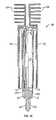
- FIG. 9is a view of a preferred embodiment before thermal spreaders devised in accordance with a preferred embodiment of the present invention are appended about the module.
- a cutaway area Dis provided to enhance illustration of certain features.
- Flex circuit 12is cutaway in area “D” to illustrate internal preferred features of module 10 .
- Area “D”is shown in greater enlargement in later FIG. 10 .
- thermal sink 14 TSWithin area D are seen thermal sink 14 TS and beyond the cutaway section of thermal sink 14 TS, there is shown a part of a circuit 19 which, in the depicted preferred embodiment, is an AMB employed in FB-DIMM circuitry.
- AMB circuit 19includes AMB die 19 D and contacts 19 C.
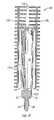
- FIG. 10is an enlarged depiction of the area D identified in FIG. 9 of an exemplar module 10 depicting in partial cutaway, details concerning the relationship between a high heat IC 19 such as an AMB 19 and substrate 14 in a preferred embodiment.
- AMB circuit 19is shown through window 250 through substrate 14 .
- AMB circuit 19is mounted on what will become the internal side 9 of flex circuit 12 relative to module 10 and is, therefore, inserted into window 250 from the “rear” relative to the perspective shown in FIG. 10 .
- Those of skillwill recognize, particularly with reference to FIG. 10 , that a portion of flex circuit 12 has been removed to expose thermal sink 14 TS and a part of 14 TS has also been cutaway.
- FIG. 11depicts an enlarged view of the area near end or edge 16 A of an exemplar module 10 . While a rounded configuration is shown, edge 16 A may take on other shapes devised to mate with various connectors or sockets. The form and function of various edge card connectors are well know in the art.
- flex 12is wrapped around edge 16 A of substrate 14 and may be laminated or adhesively connected to substrate 14 with adhesive 30 .
- the depicted adhesive 30 and flex 12may vary in thickness and are not drawn to scale to simplify the drawing.
- the depicted substrate 14has a thickness such that when assembled with the flex 12 and adhesive 30 , the thickness measured between module contacts 20 falls in the range specified for the mating connector.
- flex circuit 12may be implemented with two flex circuits 12 A and 12 B instead of one wrapped about end 16 A.
- a flex circuit 12 Amay be disposed on one side of module 10 while another flex circuit 12 B may be disposed on another side of module 10 .
- Adhesive 30is employed to attached flex circuit 12 to substrate 14 and contacts 20 are disposed on each side of module 10 .
- contacts 20need not be on both sides of module 10 and may be exhibited on only one side in configurations.
- FIG. 12is an exploded depiction of a flex circuit 12 cross-section according to one preferred embodiment of the present invention.
- the depicted flex circuit 12has four conductive layers 1201 - 1204 and seven insulative layers 1205 - 1211 .
- the numbers of layers describedare merely those used in one preferred embodiment and other numbers of layers and arrangements of layers may be employed. Even a single conductive layer flex circuit 12 may be employed in some embodiments, but flex circuits with more than one conductive layer prove to be more adaptable to more complex embodiments of the invention.
- Top conductive layer 1201 and the other conductive layersare preferably made of a conductive metal such as, for example, copper or alloy 110 .
- conductive layers 1201 , 1202 , and 1204express signal traces 1212 that make various connections by use of flex circuit 12 . These layers may also express conductive planes for ground, power or reference voltages.
- inner conductive layer 1202expresses traces connecting to and among various ICs. The function of any one of the depicted conductive layers may be interchanged in function with others of the conductive layers.
- Inner conductive layer 1203expresses a ground plane, which may be split to provide VDD return for pre-register address signals. Inner conductive layer 1203 may further express other planes and traces. In this embodiment, floods or planes at bottom conductive layer 1204 provides VREF and ground in addition to the depicted traces.
- Insulative layers 1205 and 1211are, in this embodiment, dielectric solder mask layers which may be deposited on the adjacent conductive layers for example. Other embodiments may not have such adhesive dielectric layers. Insulating layers 1206 , 1208 , and 1210 are preferably flexible dielectric substrate layers made of polyimide. However, any suitable flexible circuitry may be employed in the present invention and the depiction of FIG. 12 should be understood to be merely exemplary of one of the more complex flexible circuit structures that may be employed as flex circuit 12 .
- FIG. 13depicts another preferred embodiment in accordance with the present invention.
- the depicted module 10includes thermal spreaders 13 1 and 13 2 configured with plural extensions 13 E which reside above substrate extension 16 T and project inwardly. As those of skill will recognize, plural spreader extensions will encourage thermal shedding from the module.
- FIG. 14provides a perspective view of a module 10 shown in cross-section in prior FIG. 13 .
- FIG. 15depicts another preferred embodiment in accordance with the present invention.
- the module 10 depicted in FIG. 15exhibits plural spreader extensions above substrate extension 16 T but unlike the plural spreader extensions depicted in FIG. 13 , the spreader extensions 13 E exhibited by the module 10 depicted in FIG. 15 project outwardly.
- FIG. 16depicts a perspective view of a module 10 with plural thermal spreader extensions that project outwardly above substrate extension 16 T.
- FIG. 17depicts an exemplar module 10 that exhibits multiple radiative projects from thermal spreaders 13 1 and 13 2 to provide even more surface area for thermal shedding from module 10 .
- flex circuit 12is placed flat and both sides populated according to circuit board assembly techniques known in the art. Flex circuit 12 is then folded about end 16 A of substrate 14 . Flex 12 may be laminated or otherwise attached to substrate 14 . Adhesives are employed to secure thermal conduction between outer ICs 18 B and thermal spreaders 13 1 and 13 2 while additional thermally conductive adhesive may be employed between substrate extension 16 T and thermal spreader extensions 13 1 A and 13 2 A where such structures are employed in module 10 .
Landscapes
- Engineering & Computer Science (AREA)
- Microelectronics & Electronic Packaging (AREA)
- Cooling Or The Like Of Semiconductors Or Solid State Devices (AREA)
- Structure Of Printed Boards (AREA)
Abstract
Description
Claims (34)
Priority Applications (5)
| Application Number | Priority Date | Filing Date | Title |
|---|---|---|---|
| US11/283,355US7446410B2 (en) | 2004-09-03 | 2005-11-18 | Circuit module with thermal casing systems |
| US11/332,740US7579687B2 (en) | 2004-09-03 | 2006-01-13 | Circuit module turbulence enhancement systems and methods |
| PCT/US2006/007004WO2006121487A2 (en) | 2005-05-06 | 2006-02-28 | Circuit module with thermal casing systems and methods |
| US11/777,925US7522421B2 (en) | 2004-09-03 | 2007-07-13 | Split core circuit module |
| US12/263,060US7737549B2 (en) | 2004-09-03 | 2008-10-31 | Circuit module with thermal casing systems |
Applications Claiming Priority (9)
| Application Number | Priority Date | Filing Date | Title |
|---|---|---|---|
| US10/934,027US20060050492A1 (en) | 2004-09-03 | 2004-09-03 | Thin module system and method |
| US11/005,992US7480152B2 (en) | 2004-09-03 | 2004-12-07 | Thin module system and method |
| US11/007,551US7511968B2 (en) | 2004-09-03 | 2004-12-08 | Buffered thin module system and method |
| US11/068,688US7324352B2 (en) | 2004-09-03 | 2005-03-01 | High capacity thin module system and method |
| US11/123,721US20060053345A1 (en) | 2004-09-03 | 2005-05-06 | Thin module system and method |
| US11/193,954US20060049513A1 (en) | 2004-09-03 | 2005-07-29 | Thin module system and method with thermal management |
| PCT/US2005/028547WO2006028643A2 (en) | 2004-09-03 | 2005-08-10 | Circuit module system and method |
| US11/231,418US7443023B2 (en) | 2004-09-03 | 2005-09-21 | High capacity thin module system |
| US11/283,355US7446410B2 (en) | 2004-09-03 | 2005-11-18 | Circuit module with thermal casing systems |
Related Parent Applications (6)
| Application Number | Title | Priority Date | Filing Date |
|---|---|---|---|
| US10/934,027Continuation-In-PartUS20060050492A1 (en) | 2004-09-03 | 2004-09-03 | Thin module system and method |
| US11/005,992Continuation-In-PartUS7480152B2 (en) | 2004-09-03 | 2004-12-07 | Thin module system and method |
| US11/123,721Continuation-In-PartUS20060053345A1 (en) | 2004-09-03 | 2005-05-06 | Thin module system and method |
| US11/193,954Continuation-In-PartUS20060049513A1 (en) | 2004-09-03 | 2005-07-29 | Thin module system and method with thermal management |
| US11/231,418Continuation-In-PartUS7443023B2 (en) | 2004-09-03 | 2005-09-21 | High capacity thin module system |
| US11/255,061Continuation-In-PartUS7542297B2 (en) | 2004-09-03 | 2005-10-19 | Optimized mounting area circuit module system and method |
Related Child Applications (7)
| Application Number | Title | Priority Date | Filing Date |
|---|---|---|---|
| US11/005,992Continuation-In-PartUS7480152B2 (en) | 2004-09-03 | 2004-12-07 | Thin module system and method |
| US11/007,551Continuation-In-PartUS7511968B2 (en) | 2004-09-03 | 2004-12-08 | Buffered thin module system and method |
| US11/193,954Continuation-In-PartUS20060049513A1 (en) | 2004-09-03 | 2005-07-29 | Thin module system and method with thermal management |
| US11/332,740Continuation-In-PartUS7579687B2 (en) | 2004-09-03 | 2006-01-13 | Circuit module turbulence enhancement systems and methods |
| US11/364,489Continuation-In-PartUS7289327B2 (en) | 2004-09-03 | 2006-02-27 | Active cooling methods and apparatus for modules |
| US11/777,925Continuation-In-PartUS7522421B2 (en) | 2004-09-03 | 2007-07-13 | Split core circuit module |
| US12/263,060ContinuationUS7737549B2 (en) | 2004-09-03 | 2008-10-31 | Circuit module with thermal casing systems |
Publications (2)
| Publication Number | Publication Date |
|---|---|
| US20060090102A1 US20060090102A1 (en) | 2006-04-27 |
| US7446410B2true US7446410B2 (en) | 2008-11-04 |
Family
ID=37397019
Family Applications (1)
| Application Number | Title | Priority Date | Filing Date |
|---|---|---|---|
| US11/283,355Expired - LifetimeUS7446410B2 (en) | 2004-09-03 | 2005-11-18 | Circuit module with thermal casing systems |
Country Status (2)
| Country | Link |
|---|---|
| US (1) | US7446410B2 (en) |
| WO (1) | WO2006121487A2 (en) |
Cited By (15)
| Publication number | Priority date | Publication date | Assignee | Title |
|---|---|---|---|---|
| US20060129888A1 (en)* | 2004-09-03 | 2006-06-15 | Staktek Group L.P. | Circuit module turbulence enhacement systems and methods |
| US20060125067A1 (en)* | 2004-09-03 | 2006-06-15 | Staktek Group L.P. | Flex circuit constructions for high capacity circuit module systems and methods |
| US20070211711A1 (en)* | 2006-03-08 | 2007-09-13 | Clayton James E | Thin multichip flex-module |
| US20080192428A1 (en)* | 2007-02-08 | 2008-08-14 | Clayton James E | Thermal management system for computers |
| US20080218974A1 (en)* | 2007-03-06 | 2008-09-11 | Gerald Keith Bartley | Method and Structure for Connecting, Stacking, and Cooling Chips on a Flexible Carrier |
| US20080278916A1 (en)* | 2007-05-11 | 2008-11-13 | Ming-Yang Hsieh | Memory Module Assembly and Heat Sink thereof |
| US20090046431A1 (en)* | 2004-09-03 | 2009-02-19 | Staktek Group L.P. | High Capacity Thin Module System |
| US20100265653A1 (en)* | 2009-04-20 | 2010-10-21 | Neumann Matthew D | Heatsinks and a spring in a baffle slot between adjacent components |
| US20120020004A1 (en)* | 2009-10-30 | 2012-01-26 | Hewlett-Packard Development Company, L.P. | Frame having frame blades that participate in cooling memory modules |
| US20120235290A1 (en)* | 2009-10-07 | 2012-09-20 | Valeo Etudes Electroniques | Power module for an automobile |
| US8588017B2 (en) | 2010-10-20 | 2013-11-19 | Samsung Electronics Co., Ltd. | Memory circuits, systems, and modules for performing DRAM refresh operations and methods of operating the same |
| US20160155681A9 (en)* | 2013-02-18 | 2016-06-02 | Triquint Semiconductor, Inc. | Package for high-power semiconductor devices |
| US20170168528A1 (en)* | 2015-12-14 | 2017-06-15 | Intel Corporation | Method to realize reconfigurable memory topology |
| US11201441B2 (en)* | 2016-08-24 | 2021-12-14 | Harting Electric Gmbh & Co. Kg | Plug-in connector |
| US20220022328A1 (en)* | 2020-07-16 | 2022-01-20 | Te Connectivity Germany Gmbh | Electronic Component with Cooling Clearance, and Assembly Method |
Families Citing this family (19)
| Publication number | Priority date | Publication date | Assignee | Title |
|---|---|---|---|---|
| US7254036B2 (en)* | 2004-04-09 | 2007-08-07 | Netlist, Inc. | High density memory module using stacked printed circuit boards |
| US20060050492A1 (en)* | 2004-09-03 | 2006-03-09 | Staktek Group, L.P. | Thin module system and method |
| US7442050B1 (en) | 2005-08-29 | 2008-10-28 | Netlist, Inc. | Circuit card with flexible connection for memory module with heat spreader |
| US7619893B1 (en) | 2006-02-17 | 2009-11-17 | Netlist, Inc. | Heat spreader for electronic modules |
| US20070258278A1 (en)* | 2006-05-05 | 2007-11-08 | Abdallah Bacha | Memory module and methods for making and using the same |
| US20080002447A1 (en)* | 2006-06-29 | 2008-01-03 | Smart Modular Technologies, Inc. | Memory supermodule utilizing point to point serial data links |
| US7715200B2 (en)* | 2007-09-28 | 2010-05-11 | Samsung Electronics Co., Ltd. | Stacked semiconductor module, method of fabricating the same, and electronic system using the same |
| US20090251857A1 (en)* | 2008-04-07 | 2009-10-08 | Qimonda Ag | System including an electronic module with a heat spreader |
| US8018723B1 (en) | 2008-04-30 | 2011-09-13 | Netlist, Inc. | Heat dissipation for electronic modules |
| CN101998808A (en)* | 2009-08-25 | 2011-03-30 | 富准精密工业(深圳)有限公司 | Heat dissipating device |
| ITMI20120711A1 (en) | 2012-04-27 | 2013-10-28 | St Microelectronics Srl | POWER DEVICE |
| ITMI20120712A1 (en) | 2012-04-27 | 2013-10-28 | St Microelectronics Srl | ELECTRONIC LOOP-MOUNTED DEVICE WITH DOUBLE HEAT SINK |
| ITMI20120713A1 (en)* | 2012-04-27 | 2013-10-28 | St Microelectronics Srl | ELECTRONIC ASSEMBLY SYSTEM THROUGH THROUGH HOLES WITH DISSIPATED ELEMENTS CLOSED AMONG THEM AGAINST INSULATING BODY |
| US9093415B2 (en)* | 2013-09-25 | 2015-07-28 | Stats Chippac Ltd. | Integrated circuit packaging system with heat spreader and method of manufacture thereof |
| US10679722B2 (en) | 2016-08-26 | 2020-06-09 | Sandisk Technologies Llc | Storage system with several integrated components and method for use therewith |
| USD868069S1 (en)* | 2017-06-29 | 2019-11-26 | V-Color Technology Inc. | Memory device |
| USD842304S1 (en)* | 2017-12-21 | 2019-03-05 | Corsair Memory, Inc. | Memory module |
| USD897345S1 (en)* | 2018-12-07 | 2020-09-29 | Sung-Yu Chen | Double-data-rate SDRAM card |
| USD954061S1 (en)* | 2018-12-07 | 2022-06-07 | Sung-Yu Chen | Double-data-rate SDRAM card |
Citations (296)
| Publication number | Priority date | Publication date | Assignee | Title |
|---|---|---|---|---|
| US3372310A (en) | 1965-04-30 | 1968-03-05 | Radiation Inc | Universal modular packages for integrated circuits |
| US3436604A (en) | 1966-04-25 | 1969-04-01 | Texas Instruments Inc | Complex integrated circuit array and method for fabricating same |
| US3582865A (en) | 1969-12-16 | 1971-06-01 | Ibm | Microcircuit module and connector |
| US3654394A (en) | 1969-07-08 | 1972-04-04 | Gordon Eng Co | Field effect transistor switch, particularly for multiplexing |
| US3704455A (en) | 1971-02-01 | 1972-11-28 | Alfred D Scarbrough | 3d-coaxial memory construction and method of making |
| US3718842A (en) | 1972-04-21 | 1973-02-27 | Texas Instruments Inc | Liquid crystal display mounting structure |
| US3727064A (en) | 1971-03-17 | 1973-04-10 | Monsanto Co | Opto-isolator devices and method for the fabrication thereof |
| US3746934A (en) | 1971-05-06 | 1973-07-17 | Siemens Ag | Stack arrangement of semiconductor chips |
| US3766439A (en) | 1972-01-12 | 1973-10-16 | Gen Electric | Electronic module using flexible printed circuit board with heat sink means |
| US3772776A (en) | 1969-12-03 | 1973-11-20 | Thomas & Betts Corp | Method of interconnecting memory plane boards |
| JPS5385159U (en) | 1976-12-15 | 1978-07-13 | ||
| US4169642A (en) | 1976-09-16 | 1979-10-02 | E. I. Du Pont De Nemours And Company | Integrated circuit connector |
| US4288841A (en) | 1979-09-20 | 1981-09-08 | Bell Telephone Laboratories, Incorporated | Double cavity semiconductor chip carrier |
| US4342069A (en) | 1979-07-02 | 1982-07-27 | Mostek Corporation | Integrated circuit package |
| JPS5896756A (en) | 1981-12-04 | 1983-06-08 | Toshiba Corp | multi-chip package |
| US4429349A (en) | 1980-09-30 | 1984-01-31 | Burroughs Corporation | Coil connector |
| US4437235A (en) | 1980-12-29 | 1984-03-20 | Honeywell Information Systems Inc. | Integrated circuit package |
| GB2130025A (en) | 1982-11-08 | 1984-05-23 | Control Data Corp | Memory board stacking module |
| US4513368A (en) | 1981-05-22 | 1985-04-23 | Data General Corporation | Digital data processing system having object-based logical memory addressing and self-structuring modular memory |
| US4547834A (en) | 1982-12-30 | 1985-10-15 | Thomson-Csf | Structure for assembling complex electronic circuits |
| US4567543A (en) | 1983-02-15 | 1986-01-28 | Motorola, Inc. | Double-sided flexible electronic circuit module |
| US4587596A (en) | 1984-04-09 | 1986-05-06 | Amp Incorporated | High density mother/daughter circuit board connector |
| US4645944A (en) | 1983-09-05 | 1987-02-24 | Matsushita Electric Industrial Co., Ltd. | MOS register for selecting among various data inputs |
| US4656605A (en) | 1983-09-02 | 1987-04-07 | Wang Laboratories, Inc. | Single in-line memory module |
| US4672421A (en) | 1984-04-02 | 1987-06-09 | Motorola, Inc. | Semiconductor packaging and method |
| US4682207A (en) | 1982-03-17 | 1987-07-21 | Fujitsu Limited | Semiconductor device including leadless packages and a base plate for mounting the leadless packages |
| US4696525A (en) | 1985-12-13 | 1987-09-29 | Amp Incorporated | Socket for stacking integrated circuit packages |
| US4709300A (en) | 1986-05-05 | 1987-11-24 | Itt Gallium Arsenide Technology Center, A Division Of Itt Corporation | Jumper for a semiconductor assembly |
| US4724611A (en) | 1985-08-23 | 1988-02-16 | Nec Corporation | Method for producing semiconductor module |
| US4727513A (en) | 1983-09-02 | 1988-02-23 | Wang Laboratories, Inc. | Signal in-line memory module |
| US4733461A (en) | 1984-12-28 | 1988-03-29 | Micro Co., Ltd. | Method of stacking printed circuit boards |
| US4739589A (en) | 1985-07-12 | 1988-04-26 | Wacker-Chemitronic Gesellschaft Fur Elektronik-Grundstoff Mbh | Process and apparatus for abrasive machining of a wafer-like workpiece |
| US4763188A (en) | 1986-08-08 | 1988-08-09 | Thomas Johnson | Packaging system for multiple semiconductor devices |
| US4771366A (en) | 1987-07-06 | 1988-09-13 | International Business Machines Corporation | Ceramic card assembly having enhanced power distribution and cooling |
| US4821007A (en) | 1987-02-06 | 1989-04-11 | Tektronix, Inc. | Strip line circuit component and method of manufacture |
| US4823234A (en) | 1985-08-16 | 1989-04-18 | Dai-Ichi Seiko Co., Ltd. | Semiconductor device and its manufacture |
| US4833568A (en) | 1988-01-29 | 1989-05-23 | Berhold G Mark | Three-dimensional circuit component assembly and method corresponding thereto |
| US4850892A (en) | 1985-12-16 | 1989-07-25 | Wang Laboratories, Inc. | Connecting apparatus for electrically connecting memory modules to a printed circuit board |
| US4862249A (en) | 1987-04-17 | 1989-08-29 | Xoc Devices, Inc. | Packaging system for stacking integrated circuits |
| US4911643A (en) | 1988-10-11 | 1990-03-27 | Beta Phase, Inc. | High density and high signal integrity connector |
| US4953060A (en) | 1989-05-05 | 1990-08-28 | Ncr Corporation | Stackable integrated circuit chip package with improved heat removal |
| US4956694A (en) | 1988-11-04 | 1990-09-11 | Dense-Pac Microsystems, Inc. | Integrated circuit chip stacking |
| US4972580A (en) | 1988-06-24 | 1990-11-27 | Kabushiki Kaisha Toshiba | Method for connecting electronic components with dummy patterns |
| US4982266A (en) | 1987-12-23 | 1991-01-01 | Texas Instruments Incorporated | Integrated circuit with metal interconnecting layers above and below active circuitry |
| US4983533A (en) | 1987-10-28 | 1991-01-08 | Irvine Sensors Corporation | High-density electronic modules - process and product |
| US4985703A (en) | 1988-02-03 | 1991-01-15 | Nec Corporation | Analog multiplexer |
| US4992849A (en) | 1989-02-15 | 1991-02-12 | Micron Technology, Inc. | Directly bonded board multiple integrated circuit module |
| US4992850A (en) | 1989-02-15 | 1991-02-12 | Micron Technology, Inc. | Directly bonded simm module |
| JPH03102862A (en) | 1989-09-18 | 1991-04-30 | Fujitsu Ltd | Semiconductor device |
| US5014161A (en) | 1985-07-22 | 1991-05-07 | Digital Equipment Corporation | System for detachably mounting semiconductors on conductor substrate |
| US5014115A (en) | 1987-11-16 | 1991-05-07 | Motorola, Inc. | Coplanar waveguide semiconductor package |
| US5016138A (en) | 1987-10-27 | 1991-05-14 | Woodman John K | Three dimensional integrated circuit package |
| US5025306A (en) | 1988-08-09 | 1991-06-18 | Texas Instruments Incorporated | Assembly of semiconductor chips |
| US5034350A (en) | 1987-09-23 | 1991-07-23 | Sgs Thomson Microelectronics S.R.L. | Semiconductor device package with dies mounted on both sides of the central pad of a metal frame |
| US5041015A (en) | 1990-03-30 | 1991-08-20 | Cal Flex, Inc. | Electrical jumper assembly |
| US5053853A (en) | 1990-05-08 | 1991-10-01 | International Business Machines Corporation | Modular electronic packaging system |
| US5065277A (en) | 1990-07-13 | 1991-11-12 | Sun Microsystems, Inc. | Three dimensional packaging arrangement for computer systems and the like |
| US5099393A (en) | 1991-03-25 | 1992-03-24 | International Business Machines Corporation | Electronic package for high density applications |
| US5104820A (en) | 1989-07-07 | 1992-04-14 | Irvine Sensors Corporation | Method of fabricating electronic circuitry unit containing stacked IC layers having lead rerouting |
| US5109318A (en) | 1990-05-07 | 1992-04-28 | International Business Machines Corporation | Pluggable electronic circuit package assembly with snap together heat sink housing |
| US5117282A (en) | 1990-10-29 | 1992-05-26 | Harris Corporation | Stacked configuration for integrated circuit devices |
| US5119269A (en) | 1989-08-23 | 1992-06-02 | Seiko Epson Corporation | Semiconductor with a battery unit |
| US5138430A (en) | 1991-06-06 | 1992-08-11 | International Business Machines Corporation | High performance versatile thermally enhanced IC chip mounting |
| US5138434A (en) | 1991-01-22 | 1992-08-11 | Micron Technology, Inc. | Packaging for semiconductor logic devices |
| US5140405A (en) | 1990-08-30 | 1992-08-18 | Micron Technology, Inc. | Semiconductor assembly utilizing elastomeric single axis conductive interconnect |
| US5159535A (en) | 1987-03-11 | 1992-10-27 | International Business Machines Corporation | Method and apparatus for mounting a flexible film semiconductor chip carrier on a circuitized substrate |
| US5173840A (en) | 1990-05-07 | 1992-12-22 | Mitsubishi Denki Kabushiki Kaisha | Molded ic card |
| JPH0529534A (en) | 1991-07-25 | 1993-02-05 | Nec Corp | Memory module |
| US5191404A (en) | 1989-12-20 | 1993-03-02 | Digital Equipment Corporation | High density memory array packaging |
| US5208729A (en) | 1992-02-14 | 1993-05-04 | International Business Machines Corporation | Multi-chip module |
| US5214845A (en) | 1992-05-11 | 1993-06-01 | Micron Technology, Inc. | Method for producing high speed integrated circuits |
| US5219377A (en) | 1992-01-17 | 1993-06-15 | Texas Instruments Incorporated | High temperature co-fired ceramic integrated phased array package |
| US5222014A (en) | 1992-03-02 | 1993-06-22 | Motorola, Inc. | Three-dimensional multi-chip pad array carrier |
| US5224023A (en) | 1992-02-10 | 1993-06-29 | Smith Gary W | Foldable electronic assembly module |
| US5229916A (en) | 1992-03-04 | 1993-07-20 | International Business Machines Corporation | Chip edge interconnect overlay element |
| US5229917A (en) | 1992-07-24 | 1993-07-20 | The United States Of America As Represented By The Secretary Of The Air Force | VLSI integration into a 3-D WSI dual composite module |
| US5239198A (en) | 1989-09-06 | 1993-08-24 | Motorola, Inc. | Overmolded semiconductor device having solder ball and edge lead connective structure |
| US5241454A (en) | 1992-01-22 | 1993-08-31 | International Business Machines Corporation | Mutlilayered flexible circuit package |
| US5241456A (en) | 1990-07-02 | 1993-08-31 | General Electric Company | Compact high density interconnect structure |
| US5247423A (en) | 1992-05-26 | 1993-09-21 | Motorola, Inc. | Stacking three dimensional leadless multi-chip module and method for making the same |
| US5252857A (en) | 1991-08-05 | 1993-10-12 | International Business Machines Corporation | Stacked DCA memory chips |
| US5259770A (en) | 1992-03-19 | 1993-11-09 | Amp Incorporated | Impedance controlled elastomeric connector |
| US5261068A (en) | 1990-05-25 | 1993-11-09 | Dell Usa L.P. | Dual path memory retrieval system for an interleaved dynamic RAM memory unit |
| US5268815A (en) | 1992-02-14 | 1993-12-07 | International Business Machines Corporation | High density, high performance memory circuit package |
| JPH05335695A (en) | 1992-06-02 | 1993-12-17 | Nec Corp | Single in-line module |
| US5276418A (en) | 1988-11-16 | 1994-01-04 | Motorola, Inc. | Flexible substrate electronic assembly |
| US5281852A (en) | 1991-12-10 | 1994-01-25 | Normington Peter J C | Semiconductor device including stacked die |
| US5289062A (en) | 1991-03-18 | 1994-02-22 | Quality Semiconductor, Inc. | Fast transmission gate switch |
| US5309986A (en) | 1992-11-30 | 1994-05-10 | Satomi Itoh | Heat pipe |
| US5313097A (en) | 1992-11-16 | 1994-05-17 | International Business Machines, Corp. | High density memory module |
| US5347428A (en) | 1992-12-03 | 1994-09-13 | Irvine Sensors Corporation | Module comprising IC memory stack dedicated to and structurally combined with an IC microprocessor chip |
| US5375041A (en) | 1992-12-02 | 1994-12-20 | Intel Corporation | Ra-tab array bump tab tape based I.C. package |
| US5386341A (en) | 1993-11-01 | 1995-01-31 | Motorola, Inc. | Flexible substrate folded in a U-shape with a rigidizer plate located in the notch of the U-shape |
| US5394300A (en) | 1992-09-04 | 1995-02-28 | Mitsubishi Denki Kabushiki Kaisha | Thin multilayered IC memory card |
| US5397916A (en) | 1991-12-10 | 1995-03-14 | Normington; Peter J. C. | Semiconductor device including stacked die |
| US5400003A (en) | 1992-08-19 | 1995-03-21 | Micron Technology, Inc. | Inherently impedance matched integrated circuit module |
| US5428190A (en) | 1993-07-02 | 1995-06-27 | Sheldahl, Inc. | Rigid-flex board with anisotropic interconnect and method of manufacture |
| US5438224A (en) | 1992-04-23 | 1995-08-01 | Motorola, Inc. | Integrated circuit package having a face-to-face IC chip arrangement |
| US5448511A (en) | 1994-06-01 | 1995-09-05 | Storage Technology Corporation | Memory stack with an integrated interconnect and mounting structure |
| US5477082A (en) | 1994-01-11 | 1995-12-19 | Exponential Technology, Inc. | Bi-planar multi-chip module |
| US5491612A (en) | 1995-02-21 | 1996-02-13 | Fairchild Space And Defense Corporation | Three-dimensional modular assembly of integrated circuits |
| US5502333A (en) | 1994-03-30 | 1996-03-26 | International Business Machines Corporation | Semiconductor stack structures and fabrication/sparing methods utilizing programmable spare circuit |
| US5523619A (en) | 1993-11-03 | 1996-06-04 | International Business Machines Corporation | High density memory structure |
| US5523695A (en) | 1994-08-26 | 1996-06-04 | Vlsi Technology, Inc. | Universal test socket for exposing the active surface of an integrated circuit in a die-down package |
| US5541812A (en) | 1995-05-22 | 1996-07-30 | Burns; Carmen D. | Bus communication system for stacked high density integrated circuit packages having an intermediate lead frame |
| US5572065A (en) | 1992-06-26 | 1996-11-05 | Staktek Corporation | Hermetically sealed ceramic integrated circuit heat dissipating package |
| US5600178A (en) | 1993-10-08 | 1997-02-04 | Texas Instruments Incorporated | Semiconductor package having interdigitated leads |
| US5612570A (en) | 1995-04-13 | 1997-03-18 | Dense-Pac Microsystems, Inc. | Chip stack and method of making same |
| US5631193A (en) | 1992-12-11 | 1997-05-20 | Staktek Corporation | High density lead-on-package fabrication method |
| US5642055A (en) | 1990-02-14 | 1997-06-24 | Particle Interconnect, Inc. | Electrical interconnect using particle enhanced joining of metal surfaces |
| US5644161A (en) | 1993-03-29 | 1997-07-01 | Staktek Corporation | Ultra-high density warp-resistant memory module |
| US5646446A (en) | 1995-12-22 | 1997-07-08 | Fairchild Space And Defense Corporation | Three-dimensional flexible assembly of integrated circuits |
| US5654877A (en) | 1991-08-15 | 1997-08-05 | Staktek Corporation | Lead-on-chip integrated circuit apparatus |
| US5661339A (en) | 1992-09-16 | 1997-08-26 | Clayton; James E. | Thin multichip module |
| US5686730A (en) | 1995-05-15 | 1997-11-11 | Silicon Graphics, Inc. | Dimm pair with data memory and state memory |
| US5708297A (en) | 1992-09-16 | 1998-01-13 | Clayton; James E. | Thin multichip module |
| US5714802A (en) | 1991-06-18 | 1998-02-03 | Micron Technology, Inc. | High-density electronic module |
| US5717556A (en) | 1995-04-26 | 1998-02-10 | Nec Corporation | Printed-wiring board having plural parallel-connected interconnections |
| US5729894A (en) | 1992-07-21 | 1998-03-24 | Lsi Logic Corporation | Method of assembling ball bump grid array semiconductor packages |
| US5744862A (en) | 1996-03-29 | 1998-04-28 | Mitsubishi Denki Kabushiki Kaisha | Reduced thickness semiconductor device with IC packages mounted in openings on substrate |
| US5754409A (en) | 1996-11-06 | 1998-05-19 | Dynamem, Inc. | Foldable electronic assembly module |
| US5764497A (en) | 1995-11-13 | 1998-06-09 | Minolta Co, Ltd. | Circuit board connection method and connection structure |
| US5789815A (en) | 1996-04-23 | 1998-08-04 | Motorola, Inc. | Three dimensional semiconductor package having flexible appendages |
| US5790447A (en) | 1995-05-15 | 1998-08-04 | Silicon Graphics, Inc. | High-memory capacity DIMM with data and state memory |
| US5802395A (en) | 1996-07-08 | 1998-09-01 | International Business Machines Corporation | High density memory modules with improved data bus performance |
| US5805422A (en) | 1994-09-21 | 1998-09-08 | Nec Corporation | Semiconductor package with flexible board and method of fabricating the same |
| US5835988A (en) | 1996-03-27 | 1998-11-10 | Mitsubishi Denki Kabushiki Kaisha | Packed semiconductor device with wrap around external leads |
| US5869353A (en) | 1997-11-17 | 1999-02-09 | Dense-Pac Microsystems, Inc. | Modular panel stacking process |
| US5899705A (en) | 1997-11-20 | 1999-05-04 | Akram; Salman | Stacked leads-over chip multi-chip module |
| US5917709A (en) | 1997-06-16 | 1999-06-29 | Eastman Kodak Company | Multiple circuit board assembly having an interconnect mechanism that includes a flex connector |
| US5925934A (en) | 1995-10-28 | 1999-07-20 | Institute Of Microelectronics | Low cost and highly reliable chip-sized package |
| US5926369A (en) | 1998-01-22 | 1999-07-20 | International Business Machines Corporation | Vertically integrated multi-chip circuit package with heat-sink support |
| US5949657A (en) | 1997-12-01 | 1999-09-07 | Karabatsos; Chris | Bottom or top jumpered foldable electronic assembly |
| US5953215A (en) | 1997-12-01 | 1999-09-14 | Karabatsos; Chris | Apparatus and method for improving computer memory speed and capacity |
| US5953214A (en) | 1994-03-07 | 1999-09-14 | International Business Machines Corporation | Dual substrate package assembly coupled to a conducting member |
| US5959839A (en) | 1997-01-02 | 1999-09-28 | At&T Corp | Apparatus for heat removal using a flexible backplane |
| US5963427A (en) | 1997-12-11 | 1999-10-05 | Sun Microsystems, Inc. | Multi-chip module with flexible circuit board |
| US5966287A (en)* | 1997-12-17 | 1999-10-12 | Intel Corporation | Clip on heat exchanger for a memory module and assembly method |
| US5973395A (en) | 1996-04-30 | 1999-10-26 | Yamaichi Electronics Co., Ltd. | IC package having a single wiring sheet with a lead pattern disposed thereon |
| US5995370A (en) | 1997-09-01 | 1999-11-30 | Sharp Kabushiki Kaisha | Heat-sinking arrangement for circuit elements |
| US6002589A (en) | 1997-07-21 | 1999-12-14 | Rambus Inc. | Integrated circuit package for coupling to a printed circuit board |
| US6002167A (en) | 1995-09-22 | 1999-12-14 | Hitachi Cable, Ltd. | Semiconductor device having lead on chip structure |
| US6008538A (en) | 1996-10-08 | 1999-12-28 | Micron Technology, Inc. | Method and apparatus providing redundancy for fabricating highly reliable memory modules |
| US6014316A (en) | 1997-06-13 | 2000-01-11 | Irvine Sensors Corporation | IC stack utilizing BGA contacts |
| US6021048A (en) | 1998-02-17 | 2000-02-01 | Smith; Gary W. | High speed memory module |
| US6025992A (en)* | 1999-02-11 | 2000-02-15 | International Business Machines Corp. | Integrated heat exchanger for memory module |
| US6028352A (en) | 1997-06-13 | 2000-02-22 | Irvine Sensors Corporation | IC stack utilizing secondary leadframes |
| US6028365A (en) | 1998-03-30 | 2000-02-22 | Micron Technology, Inc. | Integrated circuit package and method of fabrication |
| US6034878A (en) | 1996-12-16 | 2000-03-07 | Hitachi, Ltd. | Source-clock-synchronized memory system and memory unit |
| US6038132A (en) | 1996-12-06 | 2000-03-14 | Mitsubishi Denki Kabushiki Kaisha | Memory module |
| US6040624A (en) | 1997-10-02 | 2000-03-21 | Motorola, Inc. | Semiconductor device package and method |
| US6072233A (en) | 1998-05-04 | 2000-06-06 | Micron Technology, Inc. | Stackable ball grid array package |
| US6078515A (en) | 1998-04-14 | 2000-06-20 | Silicon Graphics, Inc. | Memory system with multiple addressing and control busses |
| US6084294A (en) | 1998-08-26 | 2000-07-04 | Mitsubishi Denki Kabushiki Kaisha | Semiconductor device comprising stacked semiconductor elements |
| US6097087A (en) | 1997-10-31 | 2000-08-01 | Micron Technology, Inc. | Semiconductor package including flex circuit, interconnects and dense array external contacts |
| US6111757A (en) | 1998-01-16 | 2000-08-29 | International Business Machines Corp. | SIMM/DIMM memory module |
| US6121676A (en) | 1996-12-13 | 2000-09-19 | Tessera, Inc. | Stacked microelectronic assembly and method therefor |
| USRE36916E (en) | 1995-03-21 | 2000-10-17 | Simple Technology Incorporated | Apparatus for stacking semiconductor chips |
| US6157541A (en) | 1997-12-30 | 2000-12-05 | Siemens Aktiengesellschaft | Stack arrangement for two semiconductor memory chips and printed board for accepting a plurality of such stack arrangements |
| US6172874B1 (en) | 1998-04-06 | 2001-01-09 | Silicon Graphics, Inc. | System for stacking of integrated circuit packages |
| US6178093B1 (en) | 1996-06-28 | 2001-01-23 | International Business Machines Corporation | Information handling system with circuit assembly having holes filled with filler material |
| US6180881B1 (en) | 1998-05-05 | 2001-01-30 | Harlan Ruben Isaak | Chip stack and method of making same |
| US6187652B1 (en) | 1998-09-14 | 2001-02-13 | Fujitsu Limited | Method of fabrication of multiple-layer high density substrate |
| JP2001077294A (en) | 1999-09-02 | 2001-03-23 | Nec Corp | Semiconductor device |
| US6205654B1 (en) | 1992-12-11 | 2001-03-27 | Staktek Group L.P. | Method of manufacturing a surface mount package |
| US6208546B1 (en) | 1996-11-12 | 2001-03-27 | Niigata Seimitsu Co., Ltd. | Memory module |
| US6208521B1 (en) | 1997-05-19 | 2001-03-27 | Nitto Denko Corporation | Film carrier and laminate type mounting structure using same |
| JP2001085592A (en) | 1999-09-17 | 2001-03-30 | Seiko Epson Corp | Semiconductor device and its manufacturing method, circuit board, and electronic equipment |
| US6215687B1 (en) | 1996-02-26 | 2001-04-10 | Hitachi, Ltd. | Semiconductor device and process for manufacturing the same |
| US6214641B1 (en) | 1996-06-25 | 2001-04-10 | Micron Technology, Inc. | Method of fabricating a multi-chip module |
| US6222739B1 (en) | 1998-01-20 | 2001-04-24 | Viking Components | High-density computer module with stacked parallel-plane packaging |
| US6222737B1 (en) | 1999-04-23 | 2001-04-24 | Dense-Pac Microsystems, Inc. | Universal package and method of forming the same |
| US6225688B1 (en) | 1997-12-11 | 2001-05-01 | Tessera, Inc. | Stacked microelectronic assembly and method therefor |
| US20010001085A1 (en) | 1999-04-16 | 2001-05-10 | Ali Hassanzadeh | Memory module with offset notches for improved insertion and memory module connector |
| US6233650B1 (en) | 1998-04-01 | 2001-05-15 | Intel Corporation | Using FET switches for large memory arrays |
| US6234820B1 (en) | 1997-07-21 | 2001-05-22 | Rambus Inc. | Method and apparatus for joining printed circuit boards |
| US6262895B1 (en) | 2000-01-13 | 2001-07-17 | John A. Forthun | Stackable chip package with flex carrier |
| US6262476B1 (en) | 1998-07-27 | 2001-07-17 | Siemens Aktiengesellschaft | Composite member composed of at least two integrated circuits and method for the manufacture of a composite member composed of at least two integrated circuits |
| US6266252B1 (en) | 1997-12-01 | 2001-07-24 | Chris Karabatsos | Apparatus and method for terminating a computer memory bus |
| US6265660B1 (en) | 1997-07-09 | 2001-07-24 | Micron Technology, Inc. | Package stack via bottom leaded plastic (BLP) packaging |
| EP1119049A2 (en) | 2000-01-18 | 2001-07-25 | Sony Corporation | Laminate type semiconductor apparatus |
| US20010013423A1 (en) | 1996-10-31 | 2001-08-16 | Hormazdyar M. Dalal | Flip chip attach on flexible circuit carrier using chip with metallic cap on solder |
| US6281577B1 (en) | 1996-06-28 | 2001-08-28 | Pac Tech-Packaging Technologies Gmbh | Chips arranged in plurality of planes and electrically connected to one another |
| US6288907B1 (en) | 1996-05-20 | 2001-09-11 | Staktek Group, L.P. | High density integrated circuit module with complex electrical interconnect rails having electrical interconnect strain relief |
| US20010026009A1 (en) | 2000-03-24 | 2001-10-04 | Kensuke Tsunesa | Semiconductor devicse, a semicinductor module loaded with said semiconductor device and a method of manufacturing said semicoductor device |
| US6300679B1 (en) | 1998-06-01 | 2001-10-09 | Semiconductor Components Industries, Llc | Flexible substrate for packaging a semiconductor component |
| US20010028588A1 (en) | 1996-11-19 | 2001-10-11 | Matsushita Electronics Corporation | Semiconductor memory |
| US20010035572A1 (en) | 1999-05-05 | 2001-11-01 | Isaak Harlan R. | Stackable flex circuit chip package and method of making same |
| US6316825B1 (en) | 1998-05-15 | 2001-11-13 | Hyundai Electronics Industries Co., Ltd. | Chip stack package utilizing a connecting hole to improve electrical connection between leadframes |
| US20010040793A1 (en)* | 2000-02-01 | 2001-11-15 | Tetsuya Inaba | Electronic device and method of producing the same |
| US6323060B1 (en) | 1999-05-05 | 2001-11-27 | Dense-Pac Microsystems, Inc. | Stackable flex circuit IC package and method of making same |
| JP2001332683A (en) | 2000-05-19 | 2001-11-30 | Nec Corp | Laminated semiconductor device and manufacturing method thereof |
| US6336262B1 (en) | 1996-10-31 | 2002-01-08 | International Business Machines Corporation | Process of forming a capacitor with multi-level interconnection technology |
| JP2002009231A (en) | 2000-06-20 | 2002-01-11 | Seiko Epson Corp | Semiconductor device |
| US20020006032A1 (en) | 2000-05-23 | 2002-01-17 | Chris Karabatsos | Low-profile registered DIMM |
| US6343020B1 (en) | 1998-12-28 | 2002-01-29 | Foxconn Precision Components Co., Ltd. | Memory module |
| US6347394B1 (en) | 1998-11-04 | 2002-02-12 | Micron Technology, Inc. | Buffering circuit embedded in an integrated circuit device module used for buffering clocks and other input signals |
| US6349050B1 (en) | 2000-10-10 | 2002-02-19 | Rambus, Inc. | Methods and systems for reducing heat flux in memory systems |
| US6357023B1 (en) | 1998-04-08 | 2002-03-12 | Kingston Technology Co. | Connector assembly for testing memory modules from the solder-side of a PC motherboard with forced hot air |
| US20020030995A1 (en) | 2000-08-07 | 2002-03-14 | Masao Shoji | Headlight |
| US6358772B2 (en) | 1997-05-02 | 2002-03-19 | Nec Corporation | Semiconductor package having semiconductor element mounting structure of semiconductor package mounted on circuit board and method of assembling semiconductor package |
| US6370668B1 (en) | 1999-07-23 | 2002-04-09 | Rambus Inc | High speed memory system capable of selectively operating in non-chip-kill and chip-kill modes |
| US6376769B1 (en) | 1999-05-18 | 2002-04-23 | Amerasia International Technology, Inc. | High-density electronic package, and method for making same |
| US6392162B1 (en) | 2000-11-10 | 2002-05-21 | Chris Karabatsos | Double-sided flexible jumper assembly and method of manufacture |
| US6404043B1 (en) | 2000-06-21 | 2002-06-11 | Dense-Pac Microsystems, Inc. | Panel stacking of BGA devices to form three-dimensional modules |
| US20020076919A1 (en) | 1998-11-13 | 2002-06-20 | Peters Michael G. | Composite interposer and method for producing a composite interposer |
| US6410857B1 (en) | 2001-03-01 | 2002-06-25 | Lockheed Martin Corporation | Signal cross-over interconnect for a double-sided circuit card assembly |
| US6424532B2 (en)* | 1998-06-12 | 2002-07-23 | Nec Corporation | Heat sink and memory module with heat sink |
| US6426560B1 (en) | 1999-08-06 | 2002-07-30 | Hitachi, Ltd. | Semiconductor device and memory module |
| US20020101261A1 (en) | 2001-02-01 | 2002-08-01 | Chris Karabatsos | Tri-directional, high-speed bus switch |
| US6433418B1 (en) | 1998-07-24 | 2002-08-13 | Fujitsu Limited | Apparatus for a vertically accumulable semiconductor device with external leads secured by a positioning mechanism |
| US6444921B1 (en) | 2000-02-03 | 2002-09-03 | Fujitsu Limited | Reduced stress and zero stress interposers for integrated-circuit chips, multichip substrates, and the like |
| US6446158B1 (en) | 1999-05-17 | 2002-09-03 | Chris Karabatsos | Memory system using FET switches to select memory banks |
| US6449159B1 (en) | 2000-05-03 | 2002-09-10 | Rambus Inc. | Semiconductor module with imbedded heat spreader |
| US6452826B1 (en) | 2000-10-26 | 2002-09-17 | Samsung Electronics Co., Ltd. | Memory module system |
| US6459152B1 (en) | 1999-10-27 | 2002-10-01 | Mitsubishi Denki Kabushiki Kaisha | Semiconductor device having a chip, reinforcing plate, and sealing material sharing a common rear surface |
| US20020139577A1 (en) | 2001-03-27 | 2002-10-03 | Miller Charles A. | In-street integrated circuit wafer via |
| US6465893B1 (en) | 1990-09-24 | 2002-10-15 | Tessera, Inc. | Stacked chip assembly |
| US20020164838A1 (en) | 2001-05-02 | 2002-11-07 | Moon Ow Chee | Flexible ball grid array chip scale packages and methods of fabrication |
| US6486544B1 (en) | 1998-09-09 | 2002-11-26 | Seiko Epson Corporation | Semiconductor device and method manufacturing the same, circuit board, and electronic instrument |
| US6489687B1 (en) | 1999-10-01 | 2002-12-03 | Seiko Epson Corporation | Semiconductor device and method of manufacturing the same, manufacturing device, circuit board, and electronic equipment |
| US20020180022A1 (en) | 1999-10-20 | 2002-12-05 | Seiko Epson Corporation | Semiconductor device |
| US20020196612A1 (en) | 2001-05-25 | 2002-12-26 | Martin Gall | Arrangement of memory chip housings on a DIMM circuit board |
| US6502161B1 (en) | 2000-01-05 | 2002-12-31 | Rambus Inc. | Memory system including a point-to-point linked memory subsystem |
| US20030002262A1 (en) | 2001-07-02 | 2003-01-02 | Martin Benisek | Electronic printed circuit board having a plurality of identically designed, housing-encapsulated semiconductor memories |
| US20030026155A1 (en) | 2001-08-01 | 2003-02-06 | Mitsubishi Denki Kabushiki Kaisha | Semiconductor memory module and register buffer device for use in the same |
| JP2003037246A (en) | 2002-05-29 | 2003-02-07 | Hitachi Ltd | Electronic components and electronic component modules |
| US6521984B2 (en) | 2000-11-07 | 2003-02-18 | Mitsubishi Denki Kabushiki Kaisha | Semiconductor module with semiconductor devices attached to upper and lower surface of a semiconductor substrate |
| US20030035328A1 (en) | 2001-08-08 | 2003-02-20 | Mitsubishi Denki Kabushiki Kaisha | Semiconductor memory device shiftable to test mode in module as well as semiconductor memory module using the same |
| US6528870B2 (en) | 2000-01-28 | 2003-03-04 | Kabushiki Kaisha Toshiba | Semiconductor device having a plurality of stacked wiring boards |
| US20030045025A1 (en) | 2000-01-26 | 2003-03-06 | Coyle Anthony L. | Method of fabricating a molded package for micromechanical devices |
| US20030049886A1 (en) | 2001-09-07 | 2003-03-13 | Salmon Peter C. | Electronic system modules and method of fabrication |
| JP2003086761A (en) | 2001-09-14 | 2003-03-20 | Casio Comput Co Ltd | Semiconductor device and manufacturing method thereof |
| JP2003086760A (en) | 2001-09-12 | 2003-03-20 | Hitachi Ltd | Semiconductor device and method of manufacturing the same |
| US6552910B1 (en) | 2000-06-28 | 2003-04-22 | Micron Technology, Inc. | Stacked-die assemblies with a plurality of microelectronic devices and methods of manufacture |
| US20030081387A1 (en) | 2001-11-01 | 2003-05-01 | Jurgen Schulz | Module and connector having multiple contact rows |
| WO2003037053A1 (en) | 2001-10-26 | 2003-05-01 | Staktek Group, L.P. | Chip scale stacking system and method |
| US20030081392A1 (en) | 2001-10-26 | 2003-05-01 | Staktek Group, L.P. | Integrated circuit stacking system and method |
| US6560117B2 (en) | 2000-06-28 | 2003-05-06 | Micron Technology, Inc. | Packaged microelectronic die assemblies and methods of manufacture |
| US20030090879A1 (en) | 2001-06-14 | 2003-05-15 | Doblar Drew G. | Dual inline memory module |
| US20030089978A1 (en) | 1999-02-26 | 2003-05-15 | Hitachi, Ltd. | Memory-module and a method of manufacturing the same |
| US20030096497A1 (en) | 2001-11-19 | 2003-05-22 | Micron Technology, Inc. | Electrode structure for use in an integrated circuit |
| US6573593B1 (en) | 1996-09-18 | 2003-06-03 | Infineon Technologies Ag | Integrated circuit with a housing accommodating the integrated circuit |
| US6572387B2 (en) | 1999-09-24 | 2003-06-03 | Staktek Group, L.P. | Flexible circuit connector for stacked chip module |
| US20030109078A1 (en) | 1996-12-03 | 2003-06-12 | Yoshikazu Takahashi | Semiconductor device, method for manufacturing the same, and method for mounting the same |
| US6588095B2 (en) | 2001-04-27 | 2003-07-08 | Hewlett-Packard Development Company, Lp. | Method of processing a device by electrophoresis coating |
| US6590282B1 (en) | 2002-04-12 | 2003-07-08 | Industrial Technology Research Institute | Stacked semiconductor package formed on a substrate and method for fabrication |
| US6600222B1 (en) | 2002-07-17 | 2003-07-29 | Intel Corporation | Stacked microelectronic packages |
| US20030159278A1 (en) | 2002-02-26 | 2003-08-28 | Peddle Charles I. | Methods and apparatus for fabricating Chip-on-Board modules |
| US6614664B2 (en) | 2000-10-24 | 2003-09-02 | Samsung Electronics Co., Ltd. | Memory module having series-connected printed circuit boards |
| US20030168725A1 (en) | 1996-12-13 | 2003-09-11 | Tessera, Inc. | Methods of making microelectronic assemblies including folded substrates |
| US6627984B2 (en) | 2001-07-24 | 2003-09-30 | Dense-Pac Microsystems, Inc. | Chip stack with differing chip package types |
| US6629855B1 (en) | 1999-07-01 | 2003-10-07 | Silicon Graphics, Inc. | Memory system including guides that receive memory modules |
| JP2003309246A (en) | 2003-05-12 | 2003-10-31 | Oki Electric Ind Co Ltd | Semiconductor module |
| JP2003347503A (en) | 2002-05-30 | 2003-12-05 | Hitachi Ltd | Semiconductor device and method of manufacturing the same, and semiconductor mounting structure |
| US6661092B2 (en) | 2001-07-26 | 2003-12-09 | Elpida Memory, Inc. | Memory module |
| US6660561B2 (en) | 2000-06-15 | 2003-12-09 | Dpac Technologies Corp. | Method of assembling a stackable integrated circuit chip |
| US20040000708A1 (en) | 2001-10-26 | 2004-01-01 | Staktek Group, L.P. | Memory expansion and chip scale stacking system and method |
| US6677670B2 (en) | 2000-04-25 | 2004-01-13 | Seiko Epson Corporation | Semiconductor device |
| US20040012991A1 (en) | 2002-07-18 | 2004-01-22 | Mitsubishi Denki Kabushiki Kaisha | Semiconductor memory module |
| US6683377B1 (en) | 2000-05-30 | 2004-01-27 | Amkor Technology, Inc. | Multi-stacked memory package |
| US20040021211A1 (en) | 2002-08-05 | 2004-02-05 | Tessera, Inc. | Microelectronic adaptors, assemblies and methods |
| US6690584B2 (en) | 2000-08-14 | 2004-02-10 | Fujitsu Limited | Information-processing device having a crossbar-board connected to back panels on different sides |
| US6721185B2 (en) | 2001-05-01 | 2004-04-13 | Sun Microsystems, Inc. | Memory module having balanced data I/O contacts pads |
| US6721181B1 (en) | 2002-09-27 | 2004-04-13 | Rockwell Automation Technologies, Inc. | Elongated heat sink for use in converter assemblies |
| US20040099938A1 (en) | 2002-09-11 | 2004-05-27 | Tessera, Inc. | Assemblies having stacked semiconductor chips and methods of making same |
| US6751113B2 (en) | 2002-03-07 | 2004-06-15 | Netlist, Inc. | Arrangement of integrated circuits in a memory module |
| US6760220B2 (en) | 2002-11-25 | 2004-07-06 | Lockheed Martin Corporation | Rugged modular PC 104 chassis with blind mate connector and forced convection cooling capabilities |
| US6762942B1 (en) | 2002-09-05 | 2004-07-13 | Gary W. Smith | Break away, high speed, folded, jumperless electronic assembly |
| US6768660B2 (en) | 2001-01-08 | 2004-07-27 | Samsung Electronics Co. Ltd. | Multi-chip memory devices and modules including independent control of memory chips |
| US20040150107A1 (en) | 2002-12-31 | 2004-08-05 | Cha Ki Bon | Stack package and fabricating method thereof |
| US20040229402A1 (en) | 2001-10-26 | 2004-11-18 | Staktek Group, L.P. | Low profile chip scale stacking system and method |
| US20040236877A1 (en) | 1997-12-17 | 2004-11-25 | Lee A. Burton | Switch/network adapter port incorporating shared memory resources selectively accessible by a direct execution logic element and one or more dense logic devices in a fully buffered dual in-line memory module format (FB-DIMM) |
| US6833981B2 (en) | 2001-06-28 | 2004-12-21 | Hitachi, Ltd. | Spin valve magnetic head with three underlayers |
| US6833984B1 (en) | 2000-05-03 | 2004-12-21 | Rambus, Inc. | Semiconductor module with serial bus connection to multiple dies |
| US20050082663A1 (en) | 2003-10-20 | 2005-04-21 | Renesas Technology Corp. | Semiconductor device and semiconductor module |
| US6884653B2 (en) | 2001-03-21 | 2005-04-26 | Micron Technology, Inc. | Folded interposer |
| US20050108468A1 (en) | 2003-11-18 | 2005-05-19 | International Business Machines Corporation | Memory device with programmable receivers to improve performance |
| US20050133897A1 (en) | 2003-12-17 | 2005-06-23 | Baek Joong-Hyun | Stack package with improved heat radiation and module having the stack package mounted thereon |
| US6956284B2 (en) | 2001-10-26 | 2005-10-18 | Staktek Group L.P. | Integrated circuit stacking system and method |
| US20050242423A1 (en) | 2001-10-26 | 2005-11-03 | Staktek Group, L.P. | Stacked module systems and methods |
| US20050263911A1 (en) | 2004-05-31 | 2005-12-01 | Yusuke Igarashi | Circuit device and manufacturing method thereof |
| US20060020740A1 (en) | 2004-07-22 | 2006-01-26 | International Business Machines Corporation | Multi-node architecture with daisy chain communication link configurable to operate in unidirectional and bidirectional modes |
| US20060053345A1 (en) | 2004-09-03 | 2006-03-09 | Staktek Group L.P. | Thin module system and method |
| US20060050492A1 (en)* | 2004-09-03 | 2006-03-09 | Staktek Group, L.P. | Thin module system and method |
| US20060049502A1 (en)* | 2004-09-03 | 2006-03-09 | Staktek Group, L.P. | Module thermal management system and method |
| US20060050497A1 (en) | 2004-09-03 | 2006-03-09 | Staktek Group L.P. | Buffered thin module system and method |
| US20060091529A1 (en) | 2004-09-03 | 2006-05-04 | Staktek Group L.P. | High capacity thin module system and method |
| US20060095592A1 (en) | 2004-10-29 | 2006-05-04 | International Business Machines Corporation | Multi-channel memory architecture for daisy chained arrangements of nodes with bridging between memory channels |
| US20060111866A1 (en) | 2004-11-23 | 2006-05-25 | Leclerg Frank E | Method, apparatus, and system for memory read transaction biasing in mirrored mode to provide thermal management |
| US7053478B2 (en) | 2001-10-26 | 2006-05-30 | Staktek Group L.P. | Pitch change and chip scale stacking system |
| US20060125067A1 (en) | 2004-09-03 | 2006-06-15 | Staktek Group L.P. | Flex circuit constructions for high capacity circuit module systems and methods |
| US7079396B2 (en)* | 2004-06-14 | 2006-07-18 | Sun Microsystems, Inc. | Memory module cooling |
| US7180167B2 (en) | 2001-10-26 | 2007-02-20 | Staktek Group L. P. | Low profile stacking system and method |
| US7289327B2 (en)* | 2006-02-27 | 2007-10-30 | Stakick Group L.P. | Active cooling methods and apparatus for modules |
| US7324352B2 (en)* | 2004-09-03 | 2008-01-29 | Staktek Group L.P. | High capacity thin module system and method |
Family Cites Families (6)
| Publication number | Priority date | Publication date | Assignee | Title |
|---|---|---|---|---|
| US4427235A (en)* | 1981-01-19 | 1984-01-24 | Ogle Petroleum Inc. Of California | Method of solution mining subsurface orebodies to reduce restoration activities |
| FR2610952B1 (en)* | 1987-02-17 | 1989-05-05 | Aerospatiale | METHOD AND MACHINE FOR KNITTING COMPOSITE REINFORCEMENTS |
| US5708287A (en)* | 1995-11-29 | 1998-01-13 | Kabushiki Kaisha Toshiba | Power semiconductor device having an active layer |
| DK1010452T3 (en)* | 1998-12-14 | 2005-12-19 | Atlas Copco Airpower Nv | Process for drying a gas |
| US6234620B1 (en)* | 1999-06-29 | 2001-05-22 | Eastman Kodak Company | Continuous ink jet printer catcher and method for making same |
| US6774653B2 (en)* | 2001-08-22 | 2004-08-10 | Sun Microsystems, Inc. | Two-pin thermal sensor calibration interface |
- 2005
- 2005-11-18USUS11/283,355patent/US7446410B2/ennot_activeExpired - Lifetime
- 2006
- 2006-02-28WOPCT/US2006/007004patent/WO2006121487A2/enactiveApplication Filing
Patent Citations (348)
| Publication number | Priority date | Publication date | Assignee | Title |
|---|---|---|---|---|
| US3372310A (en) | 1965-04-30 | 1968-03-05 | Radiation Inc | Universal modular packages for integrated circuits |
| US3436604A (en) | 1966-04-25 | 1969-04-01 | Texas Instruments Inc | Complex integrated circuit array and method for fabricating same |
| US3654394A (en) | 1969-07-08 | 1972-04-04 | Gordon Eng Co | Field effect transistor switch, particularly for multiplexing |
| US3772776A (en) | 1969-12-03 | 1973-11-20 | Thomas & Betts Corp | Method of interconnecting memory plane boards |
| US3582865A (en) | 1969-12-16 | 1971-06-01 | Ibm | Microcircuit module and connector |
| US3704455A (en) | 1971-02-01 | 1972-11-28 | Alfred D Scarbrough | 3d-coaxial memory construction and method of making |
| US3727064A (en) | 1971-03-17 | 1973-04-10 | Monsanto Co | Opto-isolator devices and method for the fabrication thereof |
| US3746934A (en) | 1971-05-06 | 1973-07-17 | Siemens Ag | Stack arrangement of semiconductor chips |
| US3766439A (en) | 1972-01-12 | 1973-10-16 | Gen Electric | Electronic module using flexible printed circuit board with heat sink means |
| US3718842A (en) | 1972-04-21 | 1973-02-27 | Texas Instruments Inc | Liquid crystal display mounting structure |
| US4169642A (en) | 1976-09-16 | 1979-10-02 | E. I. Du Pont De Nemours And Company | Integrated circuit connector |
| JPS5385159U (en) | 1976-12-15 | 1978-07-13 | ||
| US4342069A (en) | 1979-07-02 | 1982-07-27 | Mostek Corporation | Integrated circuit package |
| US4288841A (en) | 1979-09-20 | 1981-09-08 | Bell Telephone Laboratories, Incorporated | Double cavity semiconductor chip carrier |
| US4429349A (en) | 1980-09-30 | 1984-01-31 | Burroughs Corporation | Coil connector |
| US4437235A (en) | 1980-12-29 | 1984-03-20 | Honeywell Information Systems Inc. | Integrated circuit package |
| US4513368A (en) | 1981-05-22 | 1985-04-23 | Data General Corporation | Digital data processing system having object-based logical memory addressing and self-structuring modular memory |
| JPS5896756A (en) | 1981-12-04 | 1983-06-08 | Toshiba Corp | multi-chip package |
| US4682207A (en) | 1982-03-17 | 1987-07-21 | Fujitsu Limited | Semiconductor device including leadless packages and a base plate for mounting the leadless packages |
| GB2130025A (en) | 1982-11-08 | 1984-05-23 | Control Data Corp | Memory board stacking module |
| US4547834A (en) | 1982-12-30 | 1985-10-15 | Thomson-Csf | Structure for assembling complex electronic circuits |
| US4567543A (en) | 1983-02-15 | 1986-01-28 | Motorola, Inc. | Double-sided flexible electronic circuit module |
| US4727513A (en) | 1983-09-02 | 1988-02-23 | Wang Laboratories, Inc. | Signal in-line memory module |
| US4656605A (en) | 1983-09-02 | 1987-04-07 | Wang Laboratories, Inc. | Single in-line memory module |
| US4645944A (en) | 1983-09-05 | 1987-02-24 | Matsushita Electric Industrial Co., Ltd. | MOS register for selecting among various data inputs |
| US4672421A (en) | 1984-04-02 | 1987-06-09 | Motorola, Inc. | Semiconductor packaging and method |
| US4587596A (en) | 1984-04-09 | 1986-05-06 | Amp Incorporated | High density mother/daughter circuit board connector |
| US4733461A (en) | 1984-12-28 | 1988-03-29 | Micro Co., Ltd. | Method of stacking printed circuit boards |
| US4739589A (en) | 1985-07-12 | 1988-04-26 | Wacker-Chemitronic Gesellschaft Fur Elektronik-Grundstoff Mbh | Process and apparatus for abrasive machining of a wafer-like workpiece |
| US5014161A (en) | 1985-07-22 | 1991-05-07 | Digital Equipment Corporation | System for detachably mounting semiconductors on conductor substrate |
| US4823234A (en) | 1985-08-16 | 1989-04-18 | Dai-Ichi Seiko Co., Ltd. | Semiconductor device and its manufacture |
| US4724611A (en) | 1985-08-23 | 1988-02-16 | Nec Corporation | Method for producing semiconductor module |
| US4696525A (en) | 1985-12-13 | 1987-09-29 | Amp Incorporated | Socket for stacking integrated circuit packages |
| US4850892A (en) | 1985-12-16 | 1989-07-25 | Wang Laboratories, Inc. | Connecting apparatus for electrically connecting memory modules to a printed circuit board |
| US4709300A (en) | 1986-05-05 | 1987-11-24 | Itt Gallium Arsenide Technology Center, A Division Of Itt Corporation | Jumper for a semiconductor assembly |
| US4763188A (en) | 1986-08-08 | 1988-08-09 | Thomas Johnson | Packaging system for multiple semiconductor devices |
| US4821007A (en) | 1987-02-06 | 1989-04-11 | Tektronix, Inc. | Strip line circuit component and method of manufacture |
| US5159535A (en) | 1987-03-11 | 1992-10-27 | International Business Machines Corporation | Method and apparatus for mounting a flexible film semiconductor chip carrier on a circuitized substrate |
| US4862249A (en) | 1987-04-17 | 1989-08-29 | Xoc Devices, Inc. | Packaging system for stacking integrated circuits |
| EP0298211A3 (en) | 1987-07-06 | 1991-01-16 | International Business Machines Corporation | Ceramic card assembly having enhanced power distribution and cooling |
| US4771366A (en) | 1987-07-06 | 1988-09-13 | International Business Machines Corporation | Ceramic card assembly having enhanced power distribution and cooling |
| US5034350A (en) | 1987-09-23 | 1991-07-23 | Sgs Thomson Microelectronics S.R.L. | Semiconductor device package with dies mounted on both sides of the central pad of a metal frame |
| US5016138A (en) | 1987-10-27 | 1991-05-14 | Woodman John K | Three dimensional integrated circuit package |
| US4983533A (en) | 1987-10-28 | 1991-01-08 | Irvine Sensors Corporation | High-density electronic modules - process and product |
| US5014115A (en) | 1987-11-16 | 1991-05-07 | Motorola, Inc. | Coplanar waveguide semiconductor package |
| US4982266A (en) | 1987-12-23 | 1991-01-01 | Texas Instruments Incorporated | Integrated circuit with metal interconnecting layers above and below active circuitry |
| US4833568A (en) | 1988-01-29 | 1989-05-23 | Berhold G Mark | Three-dimensional circuit component assembly and method corresponding thereto |
| US4985703A (en) | 1988-02-03 | 1991-01-15 | Nec Corporation | Analog multiplexer |
| US4972580A (en) | 1988-06-24 | 1990-11-27 | Kabushiki Kaisha Toshiba | Method for connecting electronic components with dummy patterns |
| US5025306A (en) | 1988-08-09 | 1991-06-18 | Texas Instruments Incorporated | Assembly of semiconductor chips |
| US4911643A (en) | 1988-10-11 | 1990-03-27 | Beta Phase, Inc. | High density and high signal integrity connector |
| US4956694A (en) | 1988-11-04 | 1990-09-11 | Dense-Pac Microsystems, Inc. | Integrated circuit chip stacking |
| US5276418A (en) | 1988-11-16 | 1994-01-04 | Motorola, Inc. | Flexible substrate electronic assembly |
| US4992850A (en) | 1989-02-15 | 1991-02-12 | Micron Technology, Inc. | Directly bonded simm module |
| US4992849A (en) | 1989-02-15 | 1991-02-12 | Micron Technology, Inc. | Directly bonded board multiple integrated circuit module |
| US4953060A (en) | 1989-05-05 | 1990-08-28 | Ncr Corporation | Stackable integrated circuit chip package with improved heat removal |
| US5104820A (en) | 1989-07-07 | 1992-04-14 | Irvine Sensors Corporation | Method of fabricating electronic circuitry unit containing stacked IC layers having lead rerouting |
| US5119269A (en) | 1989-08-23 | 1992-06-02 | Seiko Epson Corporation | Semiconductor with a battery unit |
| US5239198A (en) | 1989-09-06 | 1993-08-24 | Motorola, Inc. | Overmolded semiconductor device having solder ball and edge lead connective structure |
| JPH03102862A (en) | 1989-09-18 | 1991-04-30 | Fujitsu Ltd | Semiconductor device |
| US5191404A (en) | 1989-12-20 | 1993-03-02 | Digital Equipment Corporation | High density memory array packaging |
| US5642055A (en) | 1990-02-14 | 1997-06-24 | Particle Interconnect, Inc. | Electrical interconnect using particle enhanced joining of metal surfaces |
| US5041015A (en) | 1990-03-30 | 1991-08-20 | Cal Flex, Inc. | Electrical jumper assembly |
| US5109318A (en) | 1990-05-07 | 1992-04-28 | International Business Machines Corporation | Pluggable electronic circuit package assembly with snap together heat sink housing |
| US5173840A (en) | 1990-05-07 | 1992-12-22 | Mitsubishi Denki Kabushiki Kaisha | Molded ic card |
| US5053853A (en) | 1990-05-08 | 1991-10-01 | International Business Machines Corporation | Modular electronic packaging system |
| US5261068A (en) | 1990-05-25 | 1993-11-09 | Dell Usa L.P. | Dual path memory retrieval system for an interleaved dynamic RAM memory unit |
| US5241456A (en) | 1990-07-02 | 1993-08-31 | General Electric Company | Compact high density interconnect structure |
| US5065277A (en) | 1990-07-13 | 1991-11-12 | Sun Microsystems, Inc. | Three dimensional packaging arrangement for computer systems and the like |
| US5140405A (en) | 1990-08-30 | 1992-08-18 | Micron Technology, Inc. | Semiconductor assembly utilizing elastomeric single axis conductive interconnect |
| US6465893B1 (en) | 1990-09-24 | 2002-10-15 | Tessera, Inc. | Stacked chip assembly |
| US5117282A (en) | 1990-10-29 | 1992-05-26 | Harris Corporation | Stacked configuration for integrated circuit devices |
| US5138434A (en) | 1991-01-22 | 1992-08-11 | Micron Technology, Inc. | Packaging for semiconductor logic devices |
| US5289062A (en) | 1991-03-18 | 1994-02-22 | Quality Semiconductor, Inc. | Fast transmission gate switch |
| US5099393A (en) | 1991-03-25 | 1992-03-24 | International Business Machines Corporation | Electronic package for high density applications |
| US5138430A (en) | 1991-06-06 | 1992-08-11 | International Business Machines Corporation | High performance versatile thermally enhanced IC chip mounting |
| US5714802A (en) | 1991-06-18 | 1998-02-03 | Micron Technology, Inc. | High-density electronic module |
| JPH0529534A (en) | 1991-07-25 | 1993-02-05 | Nec Corp | Memory module |
| US5252857A (en) | 1991-08-05 | 1993-10-12 | International Business Machines Corporation | Stacked DCA memory chips |
| US5654877A (en) | 1991-08-15 | 1997-08-05 | Staktek Corporation | Lead-on-chip integrated circuit apparatus |
| US5397916A (en) | 1991-12-10 | 1995-03-14 | Normington; Peter J. C. | Semiconductor device including stacked die |
| US5281852A (en) | 1991-12-10 | 1994-01-25 | Normington Peter J C | Semiconductor device including stacked die |
| US5219377A (en) | 1992-01-17 | 1993-06-15 | Texas Instruments Incorporated | High temperature co-fired ceramic integrated phased array package |
| US5241454A (en) | 1992-01-22 | 1993-08-31 | International Business Machines Corporation | Mutlilayered flexible circuit package |
| US5224023A (en) | 1992-02-10 | 1993-06-29 | Smith Gary W | Foldable electronic assembly module |
| US5208729A (en) | 1992-02-14 | 1993-05-04 | International Business Machines Corporation | Multi-chip module |
| US5268815A (en) | 1992-02-14 | 1993-12-07 | International Business Machines Corporation | High density, high performance memory circuit package |
| US5222014A (en) | 1992-03-02 | 1993-06-22 | Motorola, Inc. | Three-dimensional multi-chip pad array carrier |
| US5229916A (en) | 1992-03-04 | 1993-07-20 | International Business Machines Corporation | Chip edge interconnect overlay element |
| US5259770A (en) | 1992-03-19 | 1993-11-09 | Amp Incorporated | Impedance controlled elastomeric connector |
| US5438224A (en) | 1992-04-23 | 1995-08-01 | Motorola, Inc. | Integrated circuit package having a face-to-face IC chip arrangement |
| US5214845A (en) | 1992-05-11 | 1993-06-01 | Micron Technology, Inc. | Method for producing high speed integrated circuits |
| US5247423A (en) | 1992-05-26 | 1993-09-21 | Motorola, Inc. | Stacking three dimensional leadless multi-chip module and method for making the same |
| JP2821315B2 (en) | 1992-06-02 | 1998-11-05 | 日本電気株式会社 | Single inline module |
| JPH05335695A (en) | 1992-06-02 | 1993-12-17 | Nec Corp | Single in-line module |
| US5572065A (en) | 1992-06-26 | 1996-11-05 | Staktek Corporation | Hermetically sealed ceramic integrated circuit heat dissipating package |
| US5729894A (en) | 1992-07-21 | 1998-03-24 | Lsi Logic Corporation | Method of assembling ball bump grid array semiconductor packages |
| US5229917A (en) | 1992-07-24 | 1993-07-20 | The United States Of America As Represented By The Secretary Of The Air Force | VLSI integration into a 3-D WSI dual composite module |
| US5400003A (en) | 1992-08-19 | 1995-03-21 | Micron Technology, Inc. | Inherently impedance matched integrated circuit module |
| US5394300A (en) | 1992-09-04 | 1995-02-28 | Mitsubishi Denki Kabushiki Kaisha | Thin multilayered IC memory card |
| US6232659B1 (en) | 1992-09-16 | 2001-05-15 | James E. Clayton | Thin multichip module |
| US5661339A (en) | 1992-09-16 | 1997-08-26 | Clayton; James E. | Thin multichip module |
| US5708297A (en) | 1992-09-16 | 1998-01-13 | Clayton; James E. | Thin multichip module |
| US6091145A (en) | 1992-09-16 | 2000-07-18 | Clayton; James E. | Thin multichip module including a connector frame socket |
| US5751553A (en) | 1992-09-16 | 1998-05-12 | Clayton; James E. | Thin multichip module including a connector frame socket having first and second apertures |
| US6049975A (en) | 1992-09-16 | 2000-04-18 | Clayton; James E. | Method of forming a thin multichip module |
| US5731633A (en)* | 1992-09-16 | 1998-03-24 | Gary W. Hamilton | Thin multichip module |
| US5313097A (en) | 1992-11-16 | 1994-05-17 | International Business Machines, Corp. | High density memory module |
| US5309986A (en) | 1992-11-30 | 1994-05-10 | Satomi Itoh | Heat pipe |
| US5375041A (en) | 1992-12-02 | 1994-12-20 | Intel Corporation | Ra-tab array bump tab tape based I.C. package |
| US5347428A (en) | 1992-12-03 | 1994-09-13 | Irvine Sensors Corporation | Module comprising IC memory stack dedicated to and structurally combined with an IC microprocessor chip |
| US6919626B2 (en) | 1992-12-11 | 2005-07-19 | Staktek Group L.P. | High density integrated circuit module |
| US5631193A (en) | 1992-12-11 | 1997-05-20 | Staktek Corporation | High density lead-on-package fabrication method |
| US6205654B1 (en) | 1992-12-11 | 2001-03-27 | Staktek Group L.P. | Method of manufacturing a surface mount package |
| US5644161A (en) | 1993-03-29 | 1997-07-01 | Staktek Corporation | Ultra-high density warp-resistant memory module |
| US5828125A (en) | 1993-03-29 | 1998-10-27 | Staktek Corporation | Ultra-high density warp-resistant memory module |
| US5428190A (en) | 1993-07-02 | 1995-06-27 | Sheldahl, Inc. | Rigid-flex board with anisotropic interconnect and method of manufacture |
| US5600178A (en) | 1993-10-08 | 1997-02-04 | Texas Instruments Incorporated | Semiconductor package having interdigitated leads |
| US5386341A (en) | 1993-11-01 | 1995-01-31 | Motorola, Inc. | Flexible substrate folded in a U-shape with a rigidizer plate located in the notch of the U-shape |
| US5523619A (en) | 1993-11-03 | 1996-06-04 | International Business Machines Corporation | High density memory structure |
| US5477082A (en) | 1994-01-11 | 1995-12-19 | Exponential Technology, Inc. | Bi-planar multi-chip module |
| US5953214A (en) | 1994-03-07 | 1999-09-14 | International Business Machines Corporation | Dual substrate package assembly coupled to a conducting member |
| US5502333A (en) | 1994-03-30 | 1996-03-26 | International Business Machines Corporation | Semiconductor stack structures and fabrication/sparing methods utilizing programmable spare circuit |
| US5448511A (en) | 1994-06-01 | 1995-09-05 | Storage Technology Corporation | Memory stack with an integrated interconnect and mounting structure |
| US5523695A (en) | 1994-08-26 | 1996-06-04 | Vlsi Technology, Inc. | Universal test socket for exposing the active surface of an integrated circuit in a die-down package |
| US5805422A (en) | 1994-09-21 | 1998-09-08 | Nec Corporation | Semiconductor package with flexible board and method of fabricating the same |
| US5491612A (en) | 1995-02-21 | 1996-02-13 | Fairchild Space And Defense Corporation | Three-dimensional modular assembly of integrated circuits |
| USRE36916E (en) | 1995-03-21 | 2000-10-17 | Simple Technology Incorporated | Apparatus for stacking semiconductor chips |
| US5612570A (en) | 1995-04-13 | 1997-03-18 | Dense-Pac Microsystems, Inc. | Chip stack and method of making same |
| US5717556A (en) | 1995-04-26 | 1998-02-10 | Nec Corporation | Printed-wiring board having plural parallel-connected interconnections |
| US5790447A (en) | 1995-05-15 | 1998-08-04 | Silicon Graphics, Inc. | High-memory capacity DIMM with data and state memory |
| US5686730A (en) | 1995-05-15 | 1997-11-11 | Silicon Graphics, Inc. | Dimm pair with data memory and state memory |
| US5541812A (en) | 1995-05-22 | 1996-07-30 | Burns; Carmen D. | Bus communication system for stacked high density integrated circuit packages having an intermediate lead frame |
| US6002167A (en) | 1995-09-22 | 1999-12-14 | Hitachi Cable, Ltd. | Semiconductor device having lead on chip structure |
| US5925934A (en) | 1995-10-28 | 1999-07-20 | Institute Of Microelectronics | Low cost and highly reliable chip-sized package |
| US5764497A (en) | 1995-11-13 | 1998-06-09 | Minolta Co, Ltd. | Circuit board connection method and connection structure |
| US5646446A (en) | 1995-12-22 | 1997-07-08 | Fairchild Space And Defense Corporation | Three-dimensional flexible assembly of integrated circuits |
| US5776797A (en) | 1995-12-22 | 1998-07-07 | Fairchild Space And Defense Corporation | Three-dimensional flexible assembly of integrated circuits |
| US6744656B2 (en) | 1996-02-26 | 2004-06-01 | Hitachi, Ltd. | Semiconductor device and process for manufacturing the same |
| US6215687B1 (en) | 1996-02-26 | 2001-04-10 | Hitachi, Ltd. | Semiconductor device and process for manufacturing the same |
| US6288924B1 (en) | 1996-02-26 | 2001-09-11 | Hitachi, Ltd. | Semiconductor device and process for manufacturing the same |
| US20020001216A1 (en) | 1996-02-26 | 2002-01-03 | Toshio Sugano | Semiconductor device and process for manufacturing the same |
| US5835988A (en) | 1996-03-27 | 1998-11-10 | Mitsubishi Denki Kabushiki Kaisha | Packed semiconductor device with wrap around external leads |
| US5744862A (en) | 1996-03-29 | 1998-04-28 | Mitsubishi Denki Kabushiki Kaisha | Reduced thickness semiconductor device with IC packages mounted in openings on substrate |
| US5789815A (en) | 1996-04-23 | 1998-08-04 | Motorola, Inc. | Three dimensional semiconductor package having flexible appendages |
| US5973395A (en) | 1996-04-30 | 1999-10-26 | Yamaichi Electronics Co., Ltd. | IC package having a single wiring sheet with a lead pattern disposed thereon |
| US6288907B1 (en) | 1996-05-20 | 2001-09-11 | Staktek Group, L.P. | High density integrated circuit module with complex electrical interconnect rails having electrical interconnect strain relief |
| US6214641B1 (en) | 1996-06-25 | 2001-04-10 | Micron Technology, Inc. | Method of fabricating a multi-chip module |
| US6281577B1 (en) | 1996-06-28 | 2001-08-28 | Pac Tech-Packaging Technologies Gmbh | Chips arranged in plurality of planes and electrically connected to one another |
| US6178093B1 (en) | 1996-06-28 | 2001-01-23 | International Business Machines Corporation | Information handling system with circuit assembly having holes filled with filler material |
| US5802395A (en) | 1996-07-08 | 1998-09-01 | International Business Machines Corporation | High density memory modules with improved data bus performance |
| US6573593B1 (en) | 1996-09-18 | 2003-06-03 | Infineon Technologies Ag | Integrated circuit with a housing accommodating the integrated circuit |
| US6841868B2 (en) | 1996-10-08 | 2005-01-11 | Micron Technology, Inc. | Memory modules including capacity for additional memory |
| US6720652B2 (en) | 1996-10-08 | 2004-04-13 | Micron Technology, Inc. | Apparatus providing redundancy for fabricating highly reliable memory modules |
| US20020185731A1 (en) | 1996-10-08 | 2002-12-12 | Salman Akram | Method and apparatus providing redundancy for fabricating highly reliable memory modules |
| US6215181B1 (en) | 1996-10-08 | 2001-04-10 | Micron Technology, Inc. | Method and apparatus providing redundancy for fabricating highly reliable memory modules |
| US6060339A (en) | 1996-10-08 | 2000-05-09 | Micron Technology, Inc. | Method and apparatus providing redundancy for fabricating highly reliable memory modules |
| US20010052637A1 (en) | 1996-10-08 | 2001-12-20 | Salman Akram | Memory modules including capacity for additional memory |
| US6531772B2 (en) | 1996-10-08 | 2003-03-11 | Micron Technology, Inc. | Electronic system including memory module with redundant memory capability |
| US6008538A (en) | 1996-10-08 | 1999-12-28 | Micron Technology, Inc. | Method and apparatus providing redundancy for fabricating highly reliable memory modules |
| US6336262B1 (en) | 1996-10-31 | 2002-01-08 | International Business Machines Corporation | Process of forming a capacitor with multi-level interconnection technology |
| US20010013423A1 (en) | 1996-10-31 | 2001-08-16 | Hormazdyar M. Dalal | Flip chip attach on flexible circuit carrier using chip with metallic cap on solder |
| US5754409A (en) | 1996-11-06 | 1998-05-19 | Dynamem, Inc. | Foldable electronic assembly module |
| US6208546B1 (en) | 1996-11-12 | 2001-03-27 | Niigata Seimitsu Co., Ltd. | Memory module |
| US20010028588A1 (en) | 1996-11-19 | 2001-10-11 | Matsushita Electronics Corporation | Semiconductor memory |
| US20030109078A1 (en) | 1996-12-03 | 2003-06-12 | Yoshikazu Takahashi | Semiconductor device, method for manufacturing the same, and method for mounting the same |
| US6038132A (en) | 1996-12-06 | 2000-03-14 | Mitsubishi Denki Kabushiki Kaisha | Memory module |
| US20010006252A1 (en) | 1996-12-13 | 2001-07-05 | Young Kim | Stacked microelectronic assembly and method therefor |
| US20030168725A1 (en) | 1996-12-13 | 2003-09-11 | Tessera, Inc. | Methods of making microelectronic assemblies including folded substrates |
| US6699730B2 (en) | 1996-12-13 | 2004-03-02 | Tessers, Inc. | Stacked microelectronic assembly and method therefor |
| US6121676A (en) | 1996-12-13 | 2000-09-19 | Tessera, Inc. | Stacked microelectronic assembly and method therefor |
| US6034878A (en) | 1996-12-16 | 2000-03-07 | Hitachi, Ltd. | Source-clock-synchronized memory system and memory unit |
| US5959839A (en) | 1997-01-02 | 1999-09-28 | At&T Corp | Apparatus for heat removal using a flexible backplane |
| US6358772B2 (en) | 1997-05-02 | 2002-03-19 | Nec Corporation | Semiconductor package having semiconductor element mounting structure of semiconductor package mounted on circuit board and method of assembling semiconductor package |
| US6208521B1 (en) | 1997-05-19 | 2001-03-27 | Nitto Denko Corporation | Film carrier and laminate type mounting structure using same |
| US6028352A (en) | 1997-06-13 | 2000-02-22 | Irvine Sensors Corporation | IC stack utilizing secondary leadframes |
| US6014316A (en) | 1997-06-13 | 2000-01-11 | Irvine Sensors Corporation | IC stack utilizing BGA contacts |
| US5917709A (en) | 1997-06-16 | 1999-06-29 | Eastman Kodak Company | Multiple circuit board assembly having an interconnect mechanism that includes a flex connector |
| US6265660B1 (en) | 1997-07-09 | 2001-07-24 | Micron Technology, Inc. | Package stack via bottom leaded plastic (BLP) packaging |
| US6002589A (en) | 1997-07-21 | 1999-12-14 | Rambus Inc. | Integrated circuit package for coupling to a printed circuit board |
| US6234820B1 (en) | 1997-07-21 | 2001-05-22 | Rambus Inc. | Method and apparatus for joining printed circuit boards |
| US5995370A (en) | 1997-09-01 | 1999-11-30 | Sharp Kabushiki Kaisha | Heat-sinking arrangement for circuit elements |
| US6040624A (en) | 1997-10-02 | 2000-03-21 | Motorola, Inc. | Semiconductor device package and method |
| US6368896B2 (en) | 1997-10-31 | 2002-04-09 | Micron Technology, Inc. | Method of wafer level chip scale packaging |
| US6465877B1 (en) | 1997-10-31 | 2002-10-15 | Micron Technology, Inc. | Semiconductor package including flex circuit, interconnects and dense array external contacts |
| US6097087A (en) | 1997-10-31 | 2000-08-01 | Micron Technology, Inc. | Semiconductor package including flex circuit, interconnects and dense array external contacts |
| US5869353A (en) | 1997-11-17 | 1999-02-09 | Dense-Pac Microsystems, Inc. | Modular panel stacking process |
| US5899705A (en) | 1997-11-20 | 1999-05-04 | Akram; Salman | Stacked leads-over chip multi-chip module |
| US6266252B1 (en) | 1997-12-01 | 2001-07-24 | Chris Karabatsos | Apparatus and method for terminating a computer memory bus |
| US5949657A (en) | 1997-12-01 | 1999-09-07 | Karabatsos; Chris | Bottom or top jumpered foldable electronic assembly |
| US5953215A (en) | 1997-12-01 | 1999-09-14 | Karabatsos; Chris | Apparatus and method for improving computer memory speed and capacity |
| US5963427A (en) | 1997-12-11 | 1999-10-05 | Sun Microsystems, Inc. | Multi-chip module with flexible circuit board |
| US6225688B1 (en) | 1997-12-11 | 2001-05-01 | Tessera, Inc. | Stacked microelectronic assembly and method therefor |
| US20040236877A1 (en) | 1997-12-17 | 2004-11-25 | Lee A. Burton | Switch/network adapter port incorporating shared memory resources selectively accessible by a direct execution logic element and one or more dense logic devices in a fully buffered dual in-line memory module format (FB-DIMM) |
| US5966287A (en)* | 1997-12-17 | 1999-10-12 | Intel Corporation | Clip on heat exchanger for a memory module and assembly method |
| US6157541A (en) | 1997-12-30 | 2000-12-05 | Siemens Aktiengesellschaft | Stack arrangement for two semiconductor memory chips and printed board for accepting a plurality of such stack arrangements |
| US6111757A (en) | 1998-01-16 | 2000-08-29 | International Business Machines Corp. | SIMM/DIMM memory module |
| US6222739B1 (en) | 1998-01-20 | 2001-04-24 | Viking Components | High-density computer module with stacked parallel-plane packaging |
| US5926369A (en) | 1998-01-22 | 1999-07-20 | International Business Machines Corporation | Vertically integrated multi-chip circuit package with heat-sink support |
| US6021048A (en) | 1998-02-17 | 2000-02-01 | Smith; Gary W. | High speed memory module |
| US6028365A (en) | 1998-03-30 | 2000-02-22 | Micron Technology, Inc. | Integrated circuit package and method of fabrication |
| US6233650B1 (en) | 1998-04-01 | 2001-05-15 | Intel Corporation | Using FET switches for large memory arrays |
| US6172874B1 (en) | 1998-04-06 | 2001-01-09 | Silicon Graphics, Inc. | System for stacking of integrated circuit packages |
| US6357023B1 (en) | 1998-04-08 | 2002-03-12 | Kingston Technology Co. | Connector assembly for testing memory modules from the solder-side of a PC motherboard with forced hot air |
| US6078515A (en) | 1998-04-14 | 2000-06-20 | Silicon Graphics, Inc. | Memory system with multiple addressing and control busses |
| US6072233A (en) | 1998-05-04 | 2000-06-06 | Micron Technology, Inc. | Stackable ball grid array package |
| US6180881B1 (en) | 1998-05-05 | 2001-01-30 | Harlan Ruben Isaak | Chip stack and method of making same |
| US6316825B1 (en) | 1998-05-15 | 2001-11-13 | Hyundai Electronics Industries Co., Ltd. | Chip stack package utilizing a connecting hole to improve electrical connection between leadframes |
| US6300679B1 (en) | 1998-06-01 | 2001-10-09 | Semiconductor Components Industries, Llc | Flexible substrate for packaging a semiconductor component |
| US6424532B2 (en)* | 1998-06-12 | 2002-07-23 | Nec Corporation | Heat sink and memory module with heat sink |
| US6433418B1 (en) | 1998-07-24 | 2002-08-13 | Fujitsu Limited | Apparatus for a vertically accumulable semiconductor device with external leads secured by a positioning mechanism |
| US6262476B1 (en) | 1998-07-27 | 2001-07-17 | Siemens Aktiengesellschaft | Composite member composed of at least two integrated circuits and method for the manufacture of a composite member composed of at least two integrated circuits |
| US6084294A (en) | 1998-08-26 | 2000-07-04 | Mitsubishi Denki Kabushiki Kaisha | Semiconductor device comprising stacked semiconductor elements |
| US6486544B1 (en) | 1998-09-09 | 2002-11-26 | Seiko Epson Corporation | Semiconductor device and method manufacturing the same, circuit board, and electronic instrument |
| US6187652B1 (en) | 1998-09-14 | 2001-02-13 | Fujitsu Limited | Method of fabrication of multiple-layer high density substrate |
| US6347394B1 (en) | 1998-11-04 | 2002-02-12 | Micron Technology, Inc. | Buffering circuit embedded in an integrated circuit device module used for buffering clocks and other input signals |
| US20020076919A1 (en) | 1998-11-13 | 2002-06-20 | Peters Michael G. | Composite interposer and method for producing a composite interposer |
| US6343020B1 (en) | 1998-12-28 | 2002-01-29 | Foxconn Precision Components Co., Ltd. | Memory module |
| US6025992A (en)* | 1999-02-11 | 2000-02-15 | International Business Machines Corp. | Integrated heat exchanger for memory module |
| US20030116835A1 (en) | 1999-02-26 | 2003-06-26 | Hitachi, Ltd. | Memory-module and a method of manufacturing the same |
| US20030089978A1 (en) | 1999-02-26 | 2003-05-15 | Hitachi, Ltd. | Memory-module and a method of manufacturing the same |
| US20010001085A1 (en) | 1999-04-16 | 2001-05-10 | Ali Hassanzadeh | Memory module with offset notches for improved insertion and memory module connector |
| US6428360B2 (en) | 1999-04-16 | 2002-08-06 | Sun Microsystems, Inc. | Memory module with offset notches for improved insertion and stability and memory module connector |
| US6222737B1 (en) | 1999-04-23 | 2001-04-24 | Dense-Pac Microsystems, Inc. | Universal package and method of forming the same |
| US6360433B1 (en) | 1999-04-23 | 2002-03-26 | Andrew C. Ross | Universal package and method of forming the same |
| US6514793B2 (en) | 1999-05-05 | 2003-02-04 | Dpac Technologies Corp. | Stackable flex circuit IC package and method of making same |
| US6351029B1 (en) | 1999-05-05 | 2002-02-26 | Harlan R. Isaak | Stackable flex circuit chip package and method of making same |
| US6323060B1 (en) | 1999-05-05 | 2001-11-27 | Dense-Pac Microsystems, Inc. | Stackable flex circuit IC package and method of making same |
| US6426549B1 (en) | 1999-05-05 | 2002-07-30 | Harlan R. Isaak | Stackable flex circuit IC package and method of making same |
| US20010035572A1 (en) | 1999-05-05 | 2001-11-01 | Isaak Harlan R. | Stackable flex circuit chip package and method of making same |
| US6426240B2 (en) | 1999-05-05 | 2002-07-30 | Harlan R. Isaak | Stackable flex circuit chip package and method of making same |
| US6446158B1 (en) | 1999-05-17 | 2002-09-03 | Chris Karabatsos | Memory system using FET switches to select memory banks |
| US6376769B1 (en) | 1999-05-18 | 2002-04-23 | Amerasia International Technology, Inc. | High-density electronic package, and method for making same |
| US6629855B1 (en) | 1999-07-01 | 2003-10-07 | Silicon Graphics, Inc. | Memory system including guides that receive memory modules |
| US6370668B1 (en) | 1999-07-23 | 2002-04-09 | Rambus Inc | High speed memory system capable of selectively operating in non-chip-kill and chip-kill modes |
| US6426560B1 (en) | 1999-08-06 | 2002-07-30 | Hitachi, Ltd. | Semiconductor device and memory module |
| JP2001077294A (en) | 1999-09-02 | 2001-03-23 | Nec Corp | Semiconductor device |
| US6839266B1 (en) | 1999-09-14 | 2005-01-04 | Rambus Inc. | Memory module with offset data lines and bit line swizzle configuration |
| JP2001085592A (en) | 1999-09-17 | 2001-03-30 | Seiko Epson Corp | Semiconductor device and its manufacturing method, circuit board, and electronic equipment |
| US6572387B2 (en) | 1999-09-24 | 2003-06-03 | Staktek Group, L.P. | Flexible circuit connector for stacked chip module |
| US6489687B1 (en) | 1999-10-01 | 2002-12-03 | Seiko Epson Corporation | Semiconductor device and method of manufacturing the same, manufacturing device, circuit board, and electronic equipment |
| US20020180022A1 (en) | 1999-10-20 | 2002-12-05 | Seiko Epson Corporation | Semiconductor device |
| US6459152B1 (en) | 1999-10-27 | 2002-10-01 | Mitsubishi Denki Kabushiki Kaisha | Semiconductor device having a chip, reinforcing plate, and sealing material sharing a common rear surface |
| US6502161B1 (en) | 2000-01-05 | 2002-12-31 | Rambus Inc. | Memory system including a point-to-point linked memory subsystem |
| US6473308B2 (en) | 2000-01-13 | 2002-10-29 | John A. Forthun | Stackable chip package with flex carrier |
| US20010015487A1 (en) | 2000-01-13 | 2001-08-23 | Forthun John A. | Stackable chip package with flex carrier |
| US6262895B1 (en) | 2000-01-13 | 2001-07-17 | John A. Forthun | Stackable chip package with flex carrier |
| EP1119049A2 (en) | 2000-01-18 | 2001-07-25 | Sony Corporation | Laminate type semiconductor apparatus |
| US6462412B2 (en) | 2000-01-18 | 2002-10-08 | Sony Corporation | Foldable, flexible laminate type semiconductor apparatus with reinforcing and heat-radiating plates |
| US20030045025A1 (en) | 2000-01-26 | 2003-03-06 | Coyle Anthony L. | Method of fabricating a molded package for micromechanical devices |
| US6528870B2 (en) | 2000-01-28 | 2003-03-04 | Kabushiki Kaisha Toshiba | Semiconductor device having a plurality of stacked wiring boards |
| US20010040793A1 (en)* | 2000-02-01 | 2001-11-15 | Tetsuya Inaba | Electronic device and method of producing the same |
| US6444921B1 (en) | 2000-02-03 | 2002-09-03 | Fujitsu Limited | Reduced stress and zero stress interposers for integrated-circuit chips, multichip substrates, and the like |
| US20010026009A1 (en) | 2000-03-24 | 2001-10-04 | Kensuke Tsunesa | Semiconductor devicse, a semicinductor module loaded with said semiconductor device and a method of manufacturing said semicoductor device |
| US6756661B2 (en) | 2000-03-24 | 2004-06-29 | Hitachi, Ltd. | Semiconductor device, a semiconductor module loaded with said semiconductor device and a method of manufacturing said semiconductor device |
| US6677670B2 (en) | 2000-04-25 | 2004-01-13 | Seiko Epson Corporation | Semiconductor device |
| US6833984B1 (en) | 2000-05-03 | 2004-12-21 | Rambus, Inc. | Semiconductor module with serial bus connection to multiple dies |
| US6449159B1 (en) | 2000-05-03 | 2002-09-10 | Rambus Inc. | Semiconductor module with imbedded heat spreader |
| JP2001332683A (en) | 2000-05-19 | 2001-11-30 | Nec Corp | Laminated semiconductor device and manufacturing method thereof |
| US20020006032A1 (en) | 2000-05-23 | 2002-01-17 | Chris Karabatsos | Low-profile registered DIMM |
| US6683377B1 (en) | 2000-05-30 | 2004-01-27 | Amkor Technology, Inc. | Multi-stacked memory package |
| US6660561B2 (en) | 2000-06-15 | 2003-12-09 | Dpac Technologies Corp. | Method of assembling a stackable integrated circuit chip |
| JP2002009231A (en) | 2000-06-20 | 2002-01-11 | Seiko Epson Corp | Semiconductor device |
| US20020094603A1 (en) | 2000-06-21 | 2002-07-18 | Isaak Harlan R. | Three-dimensional memory stacking using anisotropic epoxy interconnections |
| US20030064548A1 (en) | 2000-06-21 | 2003-04-03 | Isaak Harlan R. | Panel stacking of BGA devices to form three-dimensional modules |
| US6544815B2 (en) | 2000-06-21 | 2003-04-08 | Harlan R. Isaak | Panel stacking of BGA devices to form three-dimensional modules |
| US6472735B2 (en) | 2000-06-21 | 2002-10-29 | Harlan R. Isaak | Three-dimensional memory stacking using anisotropic epoxy interconnections |
| US6878571B2 (en) | 2000-06-21 | 2005-04-12 | Staktek Group L.P. | Panel stacking of BGA devices to form three-dimensional modules |
| US6404043B1 (en) | 2000-06-21 | 2002-06-11 | Dense-Pac Microsystems, Inc. | Panel stacking of BGA devices to form three-dimensional modules |
| US6566746B2 (en) | 2000-06-21 | 2003-05-20 | Dpac Technologies, Corp. | Panel stacking of BGA devices to form three-dimensional modules |
| US6552910B1 (en) | 2000-06-28 | 2003-04-22 | Micron Technology, Inc. | Stacked-die assemblies with a plurality of microelectronic devices and methods of manufacture |
| US6560117B2 (en) | 2000-06-28 | 2003-05-06 | Micron Technology, Inc. | Packaged microelectronic die assemblies and methods of manufacture |
| US20020030995A1 (en) | 2000-08-07 | 2002-03-14 | Masao Shoji | Headlight |
| US6690584B2 (en) | 2000-08-14 | 2004-02-10 | Fujitsu Limited | Information-processing device having a crossbar-board connected to back panels on different sides |
| US6721226B2 (en) | 2000-10-10 | 2004-04-13 | Rambus, Inc. | Methods and systems for reducing heat flux in memory systems |
| US6349050B1 (en) | 2000-10-10 | 2002-02-19 | Rambus, Inc. | Methods and systems for reducing heat flux in memory systems |
| US6552948B2 (en) | 2000-10-10 | 2003-04-22 | Rambus Inc. | Methods and systems for reducing heat flux in memory systems |
| US6614664B2 (en) | 2000-10-24 | 2003-09-02 | Samsung Electronics Co., Ltd. | Memory module having series-connected printed circuit boards |
| US6452826B1 (en) | 2000-10-26 | 2002-09-17 | Samsung Electronics Co., Ltd. | Memory module system |
| US6521984B2 (en) | 2000-11-07 | 2003-02-18 | Mitsubishi Denki Kabushiki Kaisha | Semiconductor module with semiconductor devices attached to upper and lower surface of a semiconductor substrate |
| US6392162B1 (en) | 2000-11-10 | 2002-05-21 | Chris Karabatsos | Double-sided flexible jumper assembly and method of manufacture |
| US6768660B2 (en) | 2001-01-08 | 2004-07-27 | Samsung Electronics Co. Ltd. | Multi-chip memory devices and modules including independent control of memory chips |
| US20020101261A1 (en) | 2001-02-01 | 2002-08-01 | Chris Karabatsos | Tri-directional, high-speed bus switch |
| US6410857B1 (en) | 2001-03-01 | 2002-06-25 | Lockheed Martin Corporation | Signal cross-over interconnect for a double-sided circuit card assembly |
| US6884653B2 (en) | 2001-03-21 | 2005-04-26 | Micron Technology, Inc. | Folded interposer |
| US20020139577A1 (en) | 2001-03-27 | 2002-10-03 | Miller Charles A. | In-street integrated circuit wafer via |
| US6588095B2 (en) | 2001-04-27 | 2003-07-08 | Hewlett-Packard Development Company, Lp. | Method of processing a device by electrophoresis coating |
| US6721185B2 (en) | 2001-05-01 | 2004-04-13 | Sun Microsystems, Inc. | Memory module having balanced data I/O contacts pads |
| US20020164838A1 (en) | 2001-05-02 | 2002-11-07 | Moon Ow Chee | Flexible ball grid array chip scale packages and methods of fabrication |
| US20020196612A1 (en) | 2001-05-25 | 2002-12-26 | Martin Gall | Arrangement of memory chip housings on a DIMM circuit board |
| US20030090879A1 (en) | 2001-06-14 | 2003-05-15 | Doblar Drew G. | Dual inline memory module |
| US6833981B2 (en) | 2001-06-28 | 2004-12-21 | Hitachi, Ltd. | Spin valve magnetic head with three underlayers |
| US6850414B2 (en) | 2001-07-02 | 2005-02-01 | Infineon Technologies Ag | Electronic printed circuit board having a plurality of identically designed, housing-encapsulated semiconductor memories |
| US20030002262A1 (en) | 2001-07-02 | 2003-01-02 | Martin Benisek | Electronic printed circuit board having a plurality of identically designed, housing-encapsulated semiconductor memories |
| US6627984B2 (en) | 2001-07-24 | 2003-09-30 | Dense-Pac Microsystems, Inc. | Chip stack with differing chip package types |
| US6661092B2 (en) | 2001-07-26 | 2003-12-09 | Elpida Memory, Inc. | Memory module |
| US20030026155A1 (en) | 2001-08-01 | 2003-02-06 | Mitsubishi Denki Kabushiki Kaisha | Semiconductor memory module and register buffer device for use in the same |
| US20030035328A1 (en) | 2001-08-08 | 2003-02-20 | Mitsubishi Denki Kabushiki Kaisha | Semiconductor memory device shiftable to test mode in module as well as semiconductor memory module using the same |
| US6646936B2 (en) | 2001-08-08 | 2003-11-11 | Mitsubishi Denki Kabushiki Kaisha | Semiconductor memory device shiftable to test mode in module as well as semiconductor memory module using the same |
| US20030049886A1 (en) | 2001-09-07 | 2003-03-13 | Salmon Peter C. | Electronic system modules and method of fabrication |
| JP2003086760A (en) | 2001-09-12 | 2003-03-20 | Hitachi Ltd | Semiconductor device and method of manufacturing the same |
| JP2003086761A (en) | 2001-09-14 | 2003-03-20 | Casio Comput Co Ltd | Semiconductor device and manufacturing method thereof |
| US6956284B2 (en) | 2001-10-26 | 2005-10-18 | Staktek Group L.P. | Integrated circuit stacking system and method |
| US7053478B2 (en) | 2001-10-26 | 2006-05-30 | Staktek Group L.P. | Pitch change and chip scale stacking system |
| US7094632B2 (en) | 2001-10-26 | 2006-08-22 | Staktek Group L.P. | Low profile chip scale stacking system and method |
| US20050242423A1 (en) | 2001-10-26 | 2005-11-03 | Staktek Group, L.P. | Stacked module systems and methods |
| US20030081392A1 (en) | 2001-10-26 | 2003-05-01 | Staktek Group, L.P. | Integrated circuit stacking system and method |
| US6914324B2 (en) | 2001-10-26 | 2005-07-05 | Staktek Group L.P. | Memory expansion and chip scale stacking system and method |
| US7180167B2 (en) | 2001-10-26 | 2007-02-20 | Staktek Group L. P. | Low profile stacking system and method |
| US6576992B1 (en) | 2001-10-26 | 2003-06-10 | Staktek Group L.P. | Chip scale stacking system and method |
| US20040000708A1 (en) | 2001-10-26 | 2004-01-01 | Staktek Group, L.P. | Memory expansion and chip scale stacking system and method |
| WO2003037053A1 (en) | 2001-10-26 | 2003-05-01 | Staktek Group, L.P. | Chip scale stacking system and method |
| US20040229402A1 (en) | 2001-10-26 | 2004-11-18 | Staktek Group, L.P. | Low profile chip scale stacking system and method |
| US20030081387A1 (en) | 2001-11-01 | 2003-05-01 | Jurgen Schulz | Module and connector having multiple contact rows |
| US20030096497A1 (en) | 2001-11-19 | 2003-05-22 | Micron Technology, Inc. | Electrode structure for use in an integrated circuit |
| US20030159278A1 (en) | 2002-02-26 | 2003-08-28 | Peddle Charles I. | Methods and apparatus for fabricating Chip-on-Board modules |
| US6873534B2 (en) | 2002-03-07 | 2005-03-29 | Netlist, Inc. | Arrangement of integrated circuits in a memory module |
| US6751113B2 (en) | 2002-03-07 | 2004-06-15 | Netlist, Inc. | Arrangement of integrated circuits in a memory module |
| US6590282B1 (en) | 2002-04-12 | 2003-07-08 | Industrial Technology Research Institute | Stacked semiconductor package formed on a substrate and method for fabrication |
| JP2003037246A (en) | 2002-05-29 | 2003-02-07 | Hitachi Ltd | Electronic components and electronic component modules |
| JP2003347503A (en) | 2002-05-30 | 2003-12-05 | Hitachi Ltd | Semiconductor device and method of manufacturing the same, and semiconductor mounting structure |
| US6600222B1 (en) | 2002-07-17 | 2003-07-29 | Intel Corporation | Stacked microelectronic packages |
| US20040012991A1 (en) | 2002-07-18 | 2004-01-22 | Mitsubishi Denki Kabushiki Kaisha | Semiconductor memory module |
| US20040021211A1 (en) | 2002-08-05 | 2004-02-05 | Tessera, Inc. | Microelectronic adaptors, assemblies and methods |
| US6762942B1 (en) | 2002-09-05 | 2004-07-13 | Gary W. Smith | Break away, high speed, folded, jumperless electronic assembly |
| US20040099938A1 (en) | 2002-09-11 | 2004-05-27 | Tessera, Inc. | Assemblies having stacked semiconductor chips and methods of making same |
| US6721181B1 (en) | 2002-09-27 | 2004-04-13 | Rockwell Automation Technologies, Inc. | Elongated heat sink for use in converter assemblies |
| US6760220B2 (en) | 2002-11-25 | 2004-07-06 | Lockheed Martin Corporation | Rugged modular PC 104 chassis with blind mate connector and forced convection cooling capabilities |
| US20040150107A1 (en) | 2002-12-31 | 2004-08-05 | Cha Ki Bon | Stack package and fabricating method thereof |
| JP2003309246A (en) | 2003-05-12 | 2003-10-31 | Oki Electric Ind Co Ltd | Semiconductor module |
| WO2004109802A1 (en) | 2003-06-03 | 2004-12-16 | Staktek Group, L.P. | Memory expansion and integrated circuit stacking system and method |
| US20050082663A1 (en) | 2003-10-20 | 2005-04-21 | Renesas Technology Corp. | Semiconductor device and semiconductor module |
| US20050108468A1 (en) | 2003-11-18 | 2005-05-19 | International Business Machines Corporation | Memory device with programmable receivers to improve performance |
| US20050133897A1 (en) | 2003-12-17 | 2005-06-23 | Baek Joong-Hyun | Stack package with improved heat radiation and module having the stack package mounted thereon |
| US20050263911A1 (en) | 2004-05-31 | 2005-12-01 | Yusuke Igarashi | Circuit device and manufacturing method thereof |
| US7079396B2 (en)* | 2004-06-14 | 2006-07-18 | Sun Microsystems, Inc. | Memory module cooling |
| US20060020740A1 (en) | 2004-07-22 | 2006-01-26 | International Business Machines Corporation | Multi-node architecture with daisy chain communication link configurable to operate in unidirectional and bidirectional modes |
| US20060125067A1 (en) | 2004-09-03 | 2006-06-15 | Staktek Group L.P. | Flex circuit constructions for high capacity circuit module systems and methods |
| US20060091529A1 (en) | 2004-09-03 | 2006-05-04 | Staktek Group L.P. | High capacity thin module system and method |
| US20060050497A1 (en) | 2004-09-03 | 2006-03-09 | Staktek Group L.P. | Buffered thin module system and method |
| US20060053345A1 (en) | 2004-09-03 | 2006-03-09 | Staktek Group L.P. | Thin module system and method |
| US20060050496A1 (en) | 2004-09-03 | 2006-03-09 | Staktek Group L.P. | Thin module system and method |
| US20060049502A1 (en)* | 2004-09-03 | 2006-03-09 | Staktek Group, L.P. | Module thermal management system and method |
| US20060050492A1 (en)* | 2004-09-03 | 2006-03-09 | Staktek Group, L.P. | Thin module system and method |
| US7324352B2 (en)* | 2004-09-03 | 2008-01-29 | Staktek Group L.P. | High capacity thin module system and method |
| US20060095592A1 (en) | 2004-10-29 | 2006-05-04 | International Business Machines Corporation | Multi-channel memory architecture for daisy chained arrangements of nodes with bridging between memory channels |
| US20060111866A1 (en) | 2004-11-23 | 2006-05-25 | Leclerg Frank E | Method, apparatus, and system for memory read transaction biasing in mirrored mode to provide thermal management |
| US7289327B2 (en)* | 2006-02-27 | 2007-10-30 | Stakick Group L.P. | Active cooling methods and apparatus for modules |
Non-Patent Citations (28)
| Title |
|---|
| 3D Interconnection for Ultra-Dense Multichip Modules, Christian VAL, Thomson-CSF DCS Computer Division, Thierry Lemoine, Thomson-CSF RCM Radar Countermeasures Division, date unavailable. |
| Chip Scale Packaging and Redistribution, Paul A. Magill, Glenn A. Rinne, J. Daniel Mis, Wayne C. Machon, Joseph W. Baggs, Unitive Electronics Inc., date unavailable. |
| Chip Scale Review Online-An Independent Journal Dedicated to the Advancement of Chip-Scale Electronics. (Website 9 pages) Fjelstad, Joseph, Pacific Consultants L.LC., Published Jan. 2001 on Internet. |
| Complaint filed Mar. 8, 2007, in the United States District Court for the District of Massachusetts, Boston Division, Civil Action No. 07 CA 10468 DPW. |
| Dense-Pac Microsystems, 16 Magabit High Speed CMOS SRAM DPS1MX16MKn3, date unavailable. |
| Dense-Pac Microsystems, 256 Megabyte CMOS DRAM DP3ED32MS72RW5, date unavailable. |
| Dense-Pac Microsystems, Breaking Space Barriers, 3-D Technology 1993. |
| Dense-Pac Microsystems, DPS512X16A3, Ceramic 512K+6 CMOS SRAM Module, date unavailable. |
| Die Products: Ideal IC Packaging for Demanding Applications-Advanced packaging that's no bigger than the die itself brings together high performance and high reliability with small size and low cost. (Website 3 pages with 2 figures) Larry Gilg and Chris Windsor. Dec. 23, 2002. Published on Internet. |
| Flexible Printed Circuit Technology-A Versatile Interconnection Option. (Website 2 pages) Fjelstad, Joseph. Dec. 3, 2002. |
| Flexible Thinking: Examining the Flexible Circuit Tapes. (Website 2 pages) Fjelstad, Joseph., Published Apr. 20, 2000 on Internet. |
| GB 0516622.8 Search Report, May 25, 2006. |
| High Density Memory Packaging Technology High Speed Imaging Applications, Dean Frew, Texas Instruments Incorporated, date unavailable. |
| IBM Preliminary 168 Pin SDRAM Registered DIMM Functional Description & Timing Diagrams, date unavailable. |
| Letter dated Sep. 11, 2006, from Chris Karabatsos of Kentron Technologies to John Kelly, President of JEDEC Solid State Technology Association, concerning potential interferences involving U.S. Appl. No. 11/306,803. |
| Pages 19-22 of Presentation by Netlist, Aug. 2004. |
| PCT/US05/28547 International Search Report and Written Opinion, PCT, Aug. 18, 2006. |
| PCT/US05/28547 Notification Concerning Transmittal of International Preliminary Report on Patentability, Mar. 15, 2007. |
| PCT/US06/04690 International Search Report, PCT, Feb. 16, 2007. |
| PCT/US06/38720 International Search Report and Written Opinion, PCT, Apr. 5, 2007. |
| Ron Bauer, Intel. "Stacked-CSP Delivers Flexibility, Reliability, and Space-Saving Capabilities", vol. 3, Spring 2002. Published on the Internet. |
| Tessera Introduces uZ ä-Ball Stacked Memory Package for Computing and Portable Electronic Products Joyce Smaragdis, Tessera Public Relations, Sandy Skees, MCA PR (www.tessera.com/news<SUB>-</SUB>events/press<SUB>-</SUB>coverage.cfm); 2 figures that purport to be directed to the uZ ä-Ball Stacked Memory Package. Published Jul. 17, 2002 in San Jose, CA. |
| Tessera Introduces uZ ä—Ball Stacked Memory Package for Computing and Portable Electronic Products Joyce Smaragdis, Tessera Public Relations, Sandy Skees, MCA PR (www.tessera.com/news—events/press—coverage.cfm); 2 figures that purport to be directed to the uZ ä—Ball Stacked Memory Package. Published Jul. 17, 2002 in San Jose, CA. |
| Tessera Technologies, Inc.-Semiconductor Intellectual Property, Chip Scale Packaging-Website pp. (3), Internet, date unavailable. |
| Tessera uZ Ball Stack Package. 4 figures that purport to be directed to the uZ-Ball Stacked Memory, Published on the Internet, date unavailable. |
| U.S. Appl. No. 11/306,803, filed Jan. 11, 2006, Chris Karabatsos. |
| Vertically-Intergrated Package, Alvin Weinberg, Pacesetter, Inc. and W. Kinzy Jones, Florida International University, date unavailable. |
| William R. Newberry, Design Techniques for Ball Grid Arrays, Xynetix Design Systems, Inc., Portland, Maine, Published on the Internet, date unavailable. |
Cited By (30)
| Publication number | Priority date | Publication date | Assignee | Title |
|---|---|---|---|---|
| US7626259B2 (en)* | 2004-09-03 | 2009-12-01 | Entorian Technologies, Lp | Heat sink for a high capacity thin module system |
| US20060125067A1 (en)* | 2004-09-03 | 2006-06-15 | Staktek Group L.P. | Flex circuit constructions for high capacity circuit module systems and methods |
| US20060129888A1 (en)* | 2004-09-03 | 2006-06-15 | Staktek Group L.P. | Circuit module turbulence enhacement systems and methods |
| US7737549B2 (en)* | 2004-09-03 | 2010-06-15 | Entorian Technologies Lp | Circuit module with thermal casing systems |
| US20090046431A1 (en)* | 2004-09-03 | 2009-02-19 | Staktek Group L.P. | High Capacity Thin Module System |
| US7579687B2 (en)* | 2004-09-03 | 2009-08-25 | Entorian Technologies, Lp | Circuit module turbulence enhancement systems and methods |
| US7616452B2 (en)* | 2004-09-03 | 2009-11-10 | Entorian Technologies, Lp | Flex circuit constructions for high capacity circuit module systems and methods |
| US20070211711A1 (en)* | 2006-03-08 | 2007-09-13 | Clayton James E | Thin multichip flex-module |
| US20080192428A1 (en)* | 2007-02-08 | 2008-08-14 | Clayton James E | Thermal management system for computers |
| US20080218974A1 (en)* | 2007-03-06 | 2008-09-11 | Gerald Keith Bartley | Method and Structure for Connecting, Stacking, and Cooling Chips on a Flexible Carrier |
| US7675164B2 (en)* | 2007-03-06 | 2010-03-09 | International Business Machines Corporation | Method and structure for connecting, stacking, and cooling chips on a flexible carrier |
| US7679913B2 (en)* | 2007-05-11 | 2010-03-16 | Ming-Yang Hsieh | Memory module assembly and heat sink thereof |
| US20100071884A1 (en)* | 2007-05-11 | 2010-03-25 | Ming-Yang Hsieh | Memory Module Assembly and Heat Sink thereof |
| US20080278916A1 (en)* | 2007-05-11 | 2008-11-13 | Ming-Yang Hsieh | Memory Module Assembly and Heat Sink thereof |
| US7929307B2 (en)* | 2007-05-11 | 2011-04-19 | Ming-Yang Hsieh | Memory module assembly and heat sink thereof |
| US20110155363A1 (en)* | 2007-05-11 | 2011-06-30 | Ming-Yang Hsieh | Memory module assembly and heat sink thereof |
| US20100265653A1 (en)* | 2009-04-20 | 2010-10-21 | Neumann Matthew D | Heatsinks and a spring in a baffle slot between adjacent components |
| US7821785B1 (en)* | 2009-04-20 | 2010-10-26 | Hewlett-Packard Development Company, L.P. | Heatsinks and a spring in a baffle slot between adjacent components |
| US20120235290A1 (en)* | 2009-10-07 | 2012-09-20 | Valeo Etudes Electroniques | Power module for an automobile |
| US8916963B2 (en)* | 2009-10-07 | 2014-12-23 | Valeo Etudes Electroniques | Power module for an automobile |
| US20120020004A1 (en)* | 2009-10-30 | 2012-01-26 | Hewlett-Packard Development Company, L.P. | Frame having frame blades that participate in cooling memory modules |
| US8767403B2 (en)* | 2009-10-30 | 2014-07-01 | Hewlett-Packard Development Company, L.P. | Frame having frame blades that participate in cooling memory modules |
| US8588017B2 (en) | 2010-10-20 | 2013-11-19 | Samsung Electronics Co., Ltd. | Memory circuits, systems, and modules for performing DRAM refresh operations and methods of operating the same |
| US20160155681A9 (en)* | 2013-02-18 | 2016-06-02 | Triquint Semiconductor, Inc. | Package for high-power semiconductor devices |
| US9559034B2 (en)* | 2013-02-18 | 2017-01-31 | Qorvo Us, Inc. | Package for high-power semiconductor devices |
| US20170168528A1 (en)* | 2015-12-14 | 2017-06-15 | Intel Corporation | Method to realize reconfigurable memory topology |
| US9791899B2 (en)* | 2015-12-14 | 2017-10-17 | Intel Corporation | Method to realize reconfigurable memory topology |
| US11201441B2 (en)* | 2016-08-24 | 2021-12-14 | Harting Electric Gmbh & Co. Kg | Plug-in connector |
| US20220022328A1 (en)* | 2020-07-16 | 2022-01-20 | Te Connectivity Germany Gmbh | Electronic Component with Cooling Clearance, and Assembly Method |
| US12016137B2 (en)* | 2020-07-16 | 2024-06-18 | Te Connectivity Germany Gmbh | Electronic component with cooling clearance, and assembly method |
Also Published As
| Publication number | Publication date |
|---|---|
| US20060090102A1 (en) | 2006-04-27 |
| WO2006121487A3 (en) | 2007-11-22 |
| WO2006121487A2 (en) | 2006-11-16 |
Similar Documents
| Publication | Publication Date | Title |
|---|---|---|
| US7737549B2 (en) | Circuit module with thermal casing systems | |
| US7446410B2 (en) | Circuit module with thermal casing systems | |
| US7542297B2 (en) | Optimized mounting area circuit module system and method | |
| US7602613B2 (en) | Thin module system and method | |
| US7511968B2 (en) | Buffered thin module system and method | |
| US7760513B2 (en) | Modified core for circuit module system and method | |
| US7468893B2 (en) | Thin module system and method | |
| US7423885B2 (en) | Die module system | |
| US7616452B2 (en) | Flex circuit constructions for high capacity circuit module systems and methods | |
| US7522425B2 (en) | High capacity thin module system and method | |
| US20070126124A1 (en) | Memory Module System and Method | |
| US20070258217A1 (en) | Split Core Circuit Module | |
| GB2453064A (en) | Circuit module for memory expansion | |
| CN101209003A (en) | High capacity thin module system and method | |
| HK1121287B (en) | Memory module system and method |
Legal Events
| Date | Code | Title | Description |
|---|---|---|---|
| AS | Assignment | Owner name:STAKTEK GROUP L.P., TEXAS Free format text:ASSIGNMENT OF ASSIGNORS INTEREST;ASSIGNORS:WEHRLY, JR., JAMES DOUGLAS;WILDER, JAMES;WOLFE, MARK;AND OTHERS;REEL/FRAME:016812/0360;SIGNING DATES FROM 20051114 TO 20051118 | |
| STCF | Information on status: patent grant | Free format text:PATENTED CASE | |
| FEPP | Fee payment procedure | Free format text:PAYOR NUMBER ASSIGNED (ORIGINAL EVENT CODE: ASPN); ENTITY STATUS OF PATENT OWNER: LARGE ENTITY | |
| CC | Certificate of correction | ||
| AS | Assignment | Owner name:ENTORIAN TECHNOLOGIES L.P., TEXAS Free format text:CHANGE OF NAME;ASSIGNOR:STAKTEK GROUP, L.P.;REEL/FRAME:023848/0062 Effective date:20080229 | |
| FPAY | Fee payment | Year of fee payment:4 | |
| AS | Assignment | Owner name:ENTORIAN GP LLC, TEXAS Free format text:MERGER;ASSIGNOR:ENTORIAN TECHNOLOGIES L.P.;REEL/FRAME:029195/0048 Effective date:20100714 Owner name:ENTORIAN TECHNOLOGIES INC., TEXAS Free format text:MERGER;ASSIGNOR:ENTORIAN GP LLC;REEL/FRAME:029195/0114 Effective date:20100714 | |
| FEPP | Fee payment procedure | Free format text:PAYOR NUMBER ASSIGNED (ORIGINAL EVENT CODE: ASPN); ENTITY STATUS OF PATENT OWNER: LARGE ENTITY Free format text:PAYER NUMBER DE-ASSIGNED (ORIGINAL EVENT CODE: RMPN); ENTITY STATUS OF PATENT OWNER: LARGE ENTITY | |
| AS | Assignment | Owner name:OVID DATA CO. LLC, DELAWARE Free format text:ASSIGNMENT OF ASSIGNORS INTEREST;ASSIGNOR:ENTORIAN TECHNOLOGIES INC.;REEL/FRAME:029389/0672 Effective date:20121031 | |
| AS | Assignment | Owner name:TAMIRAS PER PTE. LTD., LLC, DELAWARE Free format text:MERGER;ASSIGNOR:OVID DATA CO. LLC;REEL/FRAME:037373/0481 Effective date:20150903 | |
| FPAY | Fee payment | Year of fee payment:8 | |
| MAFP | Maintenance fee payment | Free format text:PAYMENT OF MAINTENANCE FEE, 12TH YEAR, LARGE ENTITY (ORIGINAL EVENT CODE: M1553); ENTITY STATUS OF PATENT OWNER: LARGE ENTITY Year of fee payment:12 |