US7446393B2 - Co-sputter deposition of metal-doped chalcogenides - Google Patents
Co-sputter deposition of metal-doped chalcogenidesDownload PDFInfo
- Publication number
- US7446393B2 US7446393B2US11/710,517US71051707AUS7446393B2US 7446393 B2US7446393 B2US 7446393B2US 71051707 AUS71051707 AUS 71051707AUS 7446393 B2US7446393 B2US 7446393B2
- Authority
- US
- United States
- Prior art keywords
- metal
- chalcogenide glass
- silver
- memory cell
- germanium selenide
- Prior art date
- Legal status (The legal status is an assumption and is not a legal conclusion. Google has not performed a legal analysis and makes no representation as to the accuracy of the status listed.)
- Expired - Fee Related, expires
Links
- 238000004544sputter depositionMethods0.000titledescription37
- 150000004770chalcogenidesChemical class0.000titledescription3
- 229910052751metalInorganic materials0.000claimsabstractdescription91
- 239000002184metalSubstances0.000claimsabstractdescription91
- QIHHYQWNYKOHEV-UHFFFAOYSA-N4-tert-butyl-3-nitrobenzoic acidChemical compoundCC(C)(C)C1=CC=C(C(O)=O)C=C1[N+]([O-])=OQIHHYQWNYKOHEV-UHFFFAOYSA-N0.000claimsabstractdescription77
- BQCADISMDOOEFD-UHFFFAOYSA-NSilverChemical compound[Ag]BQCADISMDOOEFD-UHFFFAOYSA-N0.000claimsabstractdescription49
- 239000005387chalcogenide glassSubstances0.000claimsabstractdescription49
- 229910052709silverInorganic materials0.000claimsabstractdescription49
- 239000004332silverSubstances0.000claimsabstractdescription49
- 239000010949copperSubstances0.000claimsabstractdescription31
- RYGMFSIKBFXOCR-UHFFFAOYSA-NCopperChemical compound[Cu]RYGMFSIKBFXOCR-UHFFFAOYSA-N0.000claimsabstractdescription15
- 229910052802copperInorganic materials0.000claimsabstractdescription15
- 229910005925GexSe1-xInorganic materials0.000claimsabstract3
- 230000015654memoryEffects0.000claimsdescription53
- 210000004027cellAnatomy0.000claimsdescription23
- 210000005056cell bodyAnatomy0.000claimsdescription23
- JBQYATWDVHIOAR-UHFFFAOYSA-NtellanylidenegermaniumChemical compound[Te]=[Ge]JBQYATWDVHIOAR-UHFFFAOYSA-N0.000claimsdescription14
- 239000004020conductorSubstances0.000claimsdescription9
- 238000000034methodMethods0.000abstractdescription55
- 239000000470constituentSubstances0.000abstractdescription5
- 239000010409thin filmSubstances0.000abstractdescription3
- 239000011701zincSubstances0.000abstractdescription3
- HCHKCACWOHOZIP-UHFFFAOYSA-NZincChemical compound[Zn]HCHKCACWOHOZIP-UHFFFAOYSA-N0.000abstract1
- 229910052725zincInorganic materials0.000abstract1
- 238000000151depositionMethods0.000description63
- 230000008021depositionEffects0.000description63
- 230000008569processEffects0.000description45
- 239000011521glassSubstances0.000description19
- 239000000463materialSubstances0.000description18
- 239000011669seleniumSubstances0.000description16
- 239000010408filmSubstances0.000description14
- 239000000758substrateSubstances0.000description11
- -1arsenic selenideChemical class0.000description9
- 229910052732germaniumInorganic materials0.000description8
- GNPVGFCGXDBREM-UHFFFAOYSA-Ngermanium atomChemical compound[Ge]GNPVGFCGXDBREM-UHFFFAOYSA-N0.000description8
- BUGBHKTXTAQXES-UHFFFAOYSA-NSeleniumChemical compound[Se]BUGBHKTXTAQXES-UHFFFAOYSA-N0.000description6
- 229910052785arsenicInorganic materials0.000description6
- 238000004519manufacturing processMethods0.000description6
- 229910052711seleniumInorganic materials0.000description6
- VDNSGQQAZRMTCI-UHFFFAOYSA-NsulfanylidenegermaniumChemical compound[Ge]=SVDNSGQQAZRMTCI-UHFFFAOYSA-N0.000description6
- 230000005684electric fieldEffects0.000description5
- 239000012212insulatorSubstances0.000description5
- 230000037361pathwayEffects0.000description5
- 230000005855radiationEffects0.000description4
- PXHVJJICTQNCMI-UHFFFAOYSA-NNickelChemical compound[Ni]PXHVJJICTQNCMI-UHFFFAOYSA-N0.000description3
- 238000001465metallisationMethods0.000description3
- 239000000203mixtureSubstances0.000description3
- 150000004771selenidesChemical class0.000description3
- XKRFYHLGVUSROY-UHFFFAOYSA-NArgonChemical compound[Ar]XKRFYHLGVUSROY-UHFFFAOYSA-N0.000description2
- 229910052581Si3N4Inorganic materials0.000description2
- 230000007423decreaseEffects0.000description2
- 238000010587phase diagramMethods0.000description2
- HQVNEWCFYHHQES-UHFFFAOYSA-Nsilicon nitrideChemical compoundN12[Si]34N5[Si]62N3[Si]51N64HQVNEWCFYHHQES-UHFFFAOYSA-N0.000description2
- 238000005477sputtering targetMethods0.000description2
- 239000010936titaniumSubstances0.000description2
- RTAQQCXQSZGOHL-UHFFFAOYSA-NTitaniumChemical compound[Ti]RTAQQCXQSZGOHL-UHFFFAOYSA-N0.000description1
- 239000000654additiveSubstances0.000description1
- 230000000996additive effectEffects0.000description1
- 229910052786argonInorganic materials0.000description1
- 230000002238attenuated effectEffects0.000description1
- 238000007796conventional methodMethods0.000description1
- 238000009792diffusion processMethods0.000description1
- 230000009977dual effectEffects0.000description1
- 238000005516engineering processMethods0.000description1
- 238000007496glass formingMethods0.000description1
- 239000011261inert gasSubstances0.000description1
- 150000002500ionsChemical class0.000description1
- 229910052976metal sulfideInorganic materials0.000description1
- 238000012986modificationMethods0.000description1
- 230000004048modificationEffects0.000description1
- 229910052759nickelInorganic materials0.000description1
- 230000000149penetrating effectEffects0.000description1
- 230000004044responseEffects0.000description1
- 239000004065semiconductorSubstances0.000description1
- 229910052710siliconInorganic materials0.000description1
- 239000010703siliconSubstances0.000description1
- 230000003068static effectEffects0.000description1
- 239000000126substanceSubstances0.000description1
- 229910052719titaniumInorganic materials0.000description1
- WFKWXMTUELFFGS-UHFFFAOYSA-NtungstenChemical compound[W]WFKWXMTUELFFGS-UHFFFAOYSA-N0.000description1
- 229910052721tungstenInorganic materials0.000description1
- 239000010937tungstenSubstances0.000description1
Images


Classifications
- C—CHEMISTRY; METALLURGY
- C23—COATING METALLIC MATERIAL; COATING MATERIAL WITH METALLIC MATERIAL; CHEMICAL SURFACE TREATMENT; DIFFUSION TREATMENT OF METALLIC MATERIAL; COATING BY VACUUM EVAPORATION, BY SPUTTERING, BY ION IMPLANTATION OR BY CHEMICAL VAPOUR DEPOSITION, IN GENERAL; INHIBITING CORROSION OF METALLIC MATERIAL OR INCRUSTATION IN GENERAL
- C23C—COATING METALLIC MATERIAL; COATING MATERIAL WITH METALLIC MATERIAL; SURFACE TREATMENT OF METALLIC MATERIAL BY DIFFUSION INTO THE SURFACE, BY CHEMICAL CONVERSION OR SUBSTITUTION; COATING BY VACUUM EVAPORATION, BY SPUTTERING, BY ION IMPLANTATION OR BY CHEMICAL VAPOUR DEPOSITION, IN GENERAL
- C23C14/00—Coating by vacuum evaporation, by sputtering or by ion implantation of the coating forming material
- C23C14/22—Coating by vacuum evaporation, by sputtering or by ion implantation of the coating forming material characterised by the process of coating
- C23C14/54—Controlling or regulating the coating process
- C23C14/548—Controlling the composition
- C—CHEMISTRY; METALLURGY
- C23—COATING METALLIC MATERIAL; COATING MATERIAL WITH METALLIC MATERIAL; CHEMICAL SURFACE TREATMENT; DIFFUSION TREATMENT OF METALLIC MATERIAL; COATING BY VACUUM EVAPORATION, BY SPUTTERING, BY ION IMPLANTATION OR BY CHEMICAL VAPOUR DEPOSITION, IN GENERAL; INHIBITING CORROSION OF METALLIC MATERIAL OR INCRUSTATION IN GENERAL
- C23C—COATING METALLIC MATERIAL; COATING MATERIAL WITH METALLIC MATERIAL; SURFACE TREATMENT OF METALLIC MATERIAL BY DIFFUSION INTO THE SURFACE, BY CHEMICAL CONVERSION OR SUBSTITUTION; COATING BY VACUUM EVAPORATION, BY SPUTTERING, BY ION IMPLANTATION OR BY CHEMICAL VAPOUR DEPOSITION, IN GENERAL
- C23C14/00—Coating by vacuum evaporation, by sputtering or by ion implantation of the coating forming material
- C23C14/06—Coating by vacuum evaporation, by sputtering or by ion implantation of the coating forming material characterised by the coating material
- C23C14/0623—Sulfides, selenides or tellurides
- C—CHEMISTRY; METALLURGY
- C23—COATING METALLIC MATERIAL; COATING MATERIAL WITH METALLIC MATERIAL; CHEMICAL SURFACE TREATMENT; DIFFUSION TREATMENT OF METALLIC MATERIAL; COATING BY VACUUM EVAPORATION, BY SPUTTERING, BY ION IMPLANTATION OR BY CHEMICAL VAPOUR DEPOSITION, IN GENERAL; INHIBITING CORROSION OF METALLIC MATERIAL OR INCRUSTATION IN GENERAL
- C23C—COATING METALLIC MATERIAL; COATING MATERIAL WITH METALLIC MATERIAL; SURFACE TREATMENT OF METALLIC MATERIAL BY DIFFUSION INTO THE SURFACE, BY CHEMICAL CONVERSION OR SUBSTITUTION; COATING BY VACUUM EVAPORATION, BY SPUTTERING, BY ION IMPLANTATION OR BY CHEMICAL VAPOUR DEPOSITION, IN GENERAL
- C23C14/00—Coating by vacuum evaporation, by sputtering or by ion implantation of the coating forming material
- C23C14/22—Coating by vacuum evaporation, by sputtering or by ion implantation of the coating forming material characterised by the process of coating
- C23C14/34—Sputtering
- C23C14/3464—Sputtering using more than one target
- H—ELECTRICITY
- H10—SEMICONDUCTOR DEVICES; ELECTRIC SOLID-STATE DEVICES NOT OTHERWISE PROVIDED FOR
- H10N—ELECTRIC SOLID-STATE DEVICES NOT OTHERWISE PROVIDED FOR
- H10N70/00—Solid-state devices having no potential barriers, and specially adapted for rectifying, amplifying, oscillating or switching
- H10N70/011—Manufacture or treatment of multistable switching devices
- H10N70/021—Formation of switching materials, e.g. deposition of layers
- H10N70/026—Formation of switching materials, e.g. deposition of layers by physical vapor deposition, e.g. sputtering
- H—ELECTRICITY
- H10—SEMICONDUCTOR DEVICES; ELECTRIC SOLID-STATE DEVICES NOT OTHERWISE PROVIDED FOR
- H10N—ELECTRIC SOLID-STATE DEVICES NOT OTHERWISE PROVIDED FOR
- H10N70/00—Solid-state devices having no potential barriers, and specially adapted for rectifying, amplifying, oscillating or switching
- H10N70/20—Multistable switching devices, e.g. memristors
- H10N70/24—Multistable switching devices, e.g. memristors based on migration or redistribution of ionic species, e.g. anions, vacancies
- H10N70/245—Multistable switching devices, e.g. memristors based on migration or redistribution of ionic species, e.g. anions, vacancies the species being metal cations, e.g. programmable metallization cells
- H—ELECTRICITY
- H10—SEMICONDUCTOR DEVICES; ELECTRIC SOLID-STATE DEVICES NOT OTHERWISE PROVIDED FOR
- H10N—ELECTRIC SOLID-STATE DEVICES NOT OTHERWISE PROVIDED FOR
- H10N70/00—Solid-state devices having no potential barriers, and specially adapted for rectifying, amplifying, oscillating or switching
- H10N70/801—Constructional details of multistable switching devices
- H10N70/821—Device geometry
- H10N70/826—Device geometry adapted for essentially vertical current flow, e.g. sandwich or pillar type devices
- H—ELECTRICITY
- H10—SEMICONDUCTOR DEVICES; ELECTRIC SOLID-STATE DEVICES NOT OTHERWISE PROVIDED FOR
- H10N—ELECTRIC SOLID-STATE DEVICES NOT OTHERWISE PROVIDED FOR
- H10N70/00—Solid-state devices having no potential barriers, and specially adapted for rectifying, amplifying, oscillating or switching
- H10N70/801—Constructional details of multistable switching devices
- H10N70/881—Switching materials
- H10N70/882—Compounds of sulfur, selenium or tellurium, e.g. chalcogenides
- H10N70/8822—Sulfides, e.g. CuS
- H—ELECTRICITY
- H10—SEMICONDUCTOR DEVICES; ELECTRIC SOLID-STATE DEVICES NOT OTHERWISE PROVIDED FOR
- H10N—ELECTRIC SOLID-STATE DEVICES NOT OTHERWISE PROVIDED FOR
- H10N70/00—Solid-state devices having no potential barriers, and specially adapted for rectifying, amplifying, oscillating or switching
- H10N70/801—Constructional details of multistable switching devices
- H10N70/881—Switching materials
- H10N70/882—Compounds of sulfur, selenium or tellurium, e.g. chalcogenides
- H10N70/8825—Selenides, e.g. GeSe
Definitions
- the present inventiongenerally relates to memory technology.
- present inventionrelates to the fabrication of metal-doped chalcogenides.
- RAMrandom access memory
- DRAMdynamic random access memory
- SRAMstatic random access memory
- nonvolatile memory devicesIn contrast to the potential loss of data encountered in volatile memory devices, nonvolatile memory devices retain data for long periods of time when power is removed. Examples of nonvolatile memory devices include read only memory (ROM), programmable read only memory (PROM), erasable programmable read only memory (EPROM), electrically erasable programmable read only memory (EEPROM), and the like.
- ROMread only memory
- PROMprogrammable read only memory
- EPROMerasable programmable read only memory
- EEPROMelectrically erasable programmable read only memory
- U.S. Pat. No. 6,084,796 to Kozicki, et al., entitled “Programmable metallization cell structure and method of making same,”discloses another type of non-volatile memory device known as a programmable conductor memory cell or a programmable metallization cell (PMC).
- PMCprogrammable metallization cell
- U.S. Pat. No. 6,084,796is herein incorporated by reference in its entirety.
- Such memory cellscan be integrated into a memory device, which has been referred to as a programmable conductor random access memory (PCRAM).
- PCRAMprogrammable conductor random access memory
- a chalcogenide glass elementis doped with metal, preferably silver (Ag).
- an electric field with a first polaritycauses a conductive pathway to grow along the sidewalls or in the sidewalls of the glass element, whereas an electric field of the opposite polarity dissolves the conductive pathway back into the glass element.
- the conductive pathwayextends between electrodes at opposite ends of the glass element, the resulting short or relatively low resistance can represent a logic state, e.g., a “1” state for the memory cell, whereas the unshorted, relatively high resistance state can represent another logic state, e.g., a “0” state.
- Additional applications for a programmable metallization cellinclude use as a variable programmable resistance and a variable programmable capacitance.
- One conventional technique for producing the programmable conductor memory cellapplies silver (Ag) photodoping to a chalcogenide glass such as germanium selenide (Ge 3 Se 7 ).
- the silver (Ag) photodoping processdeposits silver (Ag) over germanium selenide (Ge 3 Se 7 ) and exposes the underlying substrate assembly to a relatively intense source of ultraviolet (UV) radiation for an extended period of time, such as 15 minutes.
- UV radiationultraviolet
- the photodoping processis relatively time-consuming and can slow semiconductor fabrication rates.
- the photodoping processcan decrease the overall process rate especially when it is repetitively applied, such as in the fabrication of a multiple layer stack.
- the extended exposure to intense UV radiationcan induce the glass to convert from an amorphous material to a crystallized material, which thereby results in reduced yields.
- Another disadvantage to producing memory cells with silver (Ag) photodoping of glassesis that relatively precise control of the amount of silver (Ag) that is photodiffused into the glass is necessary. A sufficient amount of silver (Ag) must be incorporated into the glass backbone and yet, the glass must not crystallize. If too much silver (Ag) is photodiffused into the glass, the glass crystallizes. If too little silver (Ag) were to be photodiffused into the glass, the memory cell would not switch properly.
- Another disadvantage to the photodoping processis that the ultraviolet light is attenuated by the silver film as the ultraviolet light penetrates through the silver film. Such attenuation varies exponentially with the thickness of the film. In one example, with 300 nanometers (nm) wavelength ultraviolet radiation, the intensity of the ultraviolet radiation decreases to only about 10% of its initial intensity after penetrating through 650 angstroms ( ⁇ ) of silver film. This attenuation renders photodoping to be impractical with relatively thick films, and requires relatively precise control of the thicknesses of the silver (Ag) and chalcogenide glass films. In order to form a thick film with a UV photodoping process, the UV photodoping process is disadvantageously applied repetitively to relatively thin films of silver (Ag).
- the varying attenuation of the ultraviolet lightcontinues as the silver (Ag) dopes the chalcogenide glass. Further disadvantageously, this attenuation in intensity of the ultraviolet light as the ultraviolet light penetrates material results in a non-uniform depth profile of the doped silver (Ag) in the chalcogenide glass.
- Embodiments of the present inventioninclude systems and methods that overcome the disadvantages of the prior art.
- the systems and methods described hereinallow a chalcogenide glass, such as germanium selenide (Ge x Se 1-x ), to be doped with a metal such as silver (Ag), copper (Cu), and zinc (Zn), without utilizing an ultraviolet (UV) photodoping step to dope the chalcogenide glass with the metal.
- chalcogenide glassesthat can be used include germanium sulfide (Ge x S 1-x ) and arsenic selenide (As x Se 1-x ).
- embodiments of the inventionco-sputter the metal and the chalcogenide glass and allow for relatively precise and efficient control of a constituent ratio between the doping metal and the chalcogenide glass. Further advantageously, the systems and methods enable the doping of the chalcogenide glass with a relatively high degree of depth-profile uniformity. Also, the systems and methods allow a metal concentration to be varied in a controlled manner along the thin film depth.
- One embodiment according to the present inventionis a nonvolatile memory cell including a first electrode, a second electrode, and a memory cell body disposed between the first electrode and the second electrode.
- the memory cell bodyincludes a layer of germanium selenide (Ge x Se 1-x ) that is uniformly doped over depth with a metal such as silver (Ag), copper (Cu), or zinc (Zn).
- the deposition systemincludes a deposition chamber, a first target, and a second target.
- the deposition chamberis adapted to hold the substrate assembly.
- the deposition systemis further configured to sputter metal from the first target and to sputter germanium selenide (Ge x Se 1-x ) from the second target at the same time to co-deposit the metal and the germanium selenide (Ge x Se 1-x ).
- the deposition systemsputters silver (Ag) from the first target.
- the deposition systemsputters copper (Cu) or zinc (Zn) from the first target.
- the deposition systemcan further include a control configured to control the deposition rate of the metal and the deposition rate of the germanium selenide such that the nonvolatile memory cell body is deposited at a selected ratio between the metal and the germanium selenide in the cell body.
- Another embodiment according to the present inventionis a process of fabricating a nonvolatile memory structure in a substrate assembly.
- the processincludes forming a bottom electrode, co-sputtering metal and germanium selenide (Ge x Se 1-x ), and forming a top electrode.
- a metal selenide and germanium; selenium and a mixture of a metal and germanium; or a metal, germanium, and seleniumare co-sputtered.
- Another embodiment according to the present inventionis a process of forming a layer in a substrate assembly.
- the layeris capable of supporting the growth conductive pathways in the presence of an electric field.
- the processincludes providing elemental silver (Ag) in a first sputtering target, providing germanium selenide (Ge x Se 1-x ) in a second sputtering target, selecting a first sputtering rate for silver (Ag), selecting a second sputtering rate for germanium selenide (Ge x Se 1-x ), sputtering the silver (Ag), and sputtering the germanium selenide (Ge x Se 1-x ) at the same time as sputtering the silver to produce the layer.
- the co-sputter deposition of silver (Ag) and germanium selenide (Ge x Se 1-x )allows the silver (Ag) to dope the sputtered germanium selenide (Ge x Se 1-x ) in the layer with a relatively uniform depth profile.
- the first sputtering rateis determined by selecting a first sputtering power for silver (Ag)
- the second sputtering rateis determined by selecting a second sputtering power for germanium selenide (Ge x Se 1-x ).
- the processpreferably further includes selecting a ratio between the silver (Ag) and the germanium selenide in the layer, using the ratio to determine the first sputtering rate, and using the ratio to determine the second sputtering rate.
- Another embodiment according to the present inventionis a process that controls a constituent ratio during production of a memory cell body.
- the ratiois controlled by selecting a first deposition rate of a metal such as silver (Ag), copper (Cu), or zinc (Zn) selecting a second deposition rate of germanium selenide (Ge x Se 1-x ), controlling the first deposition rate by selecting a first sputtering power used to deposit the metal, and controlling the second deposition rate by selecting a second sputtering power used to deposit the germanium selenide (Ge x Se 1-x ).
- Another embodiment according to the present inventionis a process to configure a deposition system used to fabricate a memory cell body for a nonvolatile memory cell.
- the processincludes receiving an indication of a desired constituent ratio, and calculating a deposition rate for a metal and a deposition rate for germanium selenide (Ge x Se 1-x ) that provides the desired ratio.
- the calculated deposition rate for the metalis further related to a sputter power for a metal target
- the calculated deposition rate for germanium selenide (Ge x Se 1-x )is related to a sputter power for a germanium selenide (Ge x Se 1-x ) target.
- the processconfigures the deposition system to sputter the metal from the metal target at the calculated sputter power, and configures the deposition system to sputter germanium selenide (Ge x Se 1-x ) from the germanium selenide (Ge x Se 1-x ) target with the calculated sputter power.
- the metalcan be silver (Ag), copper (Cu), or zinc (Zn).
- the processincludes storing a configuration of the deposition chamber, measuring the deposition rate for the metal versus sputter power, measuring the deposition rate for germanium selenide (Ge x Se 1-x ) versus sputter power, and storing the measured information such that it can be later retrieved by the process to configure the deposition system.
- FIG. 1schematically illustrates a co-sputter deposition system according to an embodiment of the present invention.
- FIG. 2is a schematic cross section of a memory cell with a memory cell body formed by co-sputtering a metal and germanium selenide (Ge x Se 1-x ) glass.
- FIG. 3is a flowchart that generally illustrates a process of co-sputtering metal and germanium selenide (Ge x Se 1-x ) glass.
- FIG. 4is a flowchart that generally illustrates a process of configuring a deposition system to co-sputter metal and germanium selenide (Ge x Se 1-x ) glass.
- Embodiments of the present inventionallow a chalcogenide glass such as germanium selenide (Ge x Se 1-x ) to be doped with a metal such as silver (Ag), copper (Cu), or zinc (Zn) without the performance of an ultraviolet (UV) photodoping step.
- a chalcogenide glasssuch as germanium selenide (Ge x Se 1-x )
- a metalsuch as silver (Ag), copper (Cu), or zinc (Zn) without the performance of an ultraviolet (UV) photodoping step.
- Other examples of chalcogenide glasses that can be usedinclude germanium sulfide (Ge x S 1-x ) and arsenic selenide (As x Se 1-x ). The value of x can vary in a wide range.
- xcan theoretically range from 0 to 1, the fabrication of a programmable conductor random access memory (PCRAM) should maintain the value of x such that the underlying combination of chalcogenide glass doped with the metal remains in an amorphous state. It will be understood by one of ordinary skill in the art that the value of x can depend on the amount of the metal that dopes the chalcogenide glass. The selection of a value of x will be described later in connection with FIG. 2 .
- embodiments of the inventionco-sputter the metal and the chalcogenide glass.
- Thisprovides a relatively precise and efficient control of a constituent ratio between the doping metal and the chalcogenide glass.
- the doping of the chalcogenide glass with the metalcan be produced with a relatively high degree of depth profile uniformity.
- a first typea lateral doping profile, varies depending on the deposition system. For example, variations in the projected light intensity of an ultraviolet source across the surface of the deposited film can produce lateral variations in the doping profile.
- the attenuation of the ultraviolet light as the ultraviolet light penetrates through the metal and the chalcogenide glassgives rise to variations in depth profile uniformity.
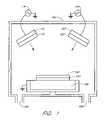
- FIG. 1schematically illustrates a co-sputter deposition system 100 according to an embodiment of the present invention.
- the illustrated co-sputter deposition system 100includes a first inlet 102 adapted to introduce an inert gas, such as argon (Ar).
- a second inlet 104allows a vacuum pump to evacuate an interior of the co-sputter deposition system 100 to a relatively low pressure.
- a first target 110provides a source of chalcogenide glass, preferably germanium selenide (Ge x Se 1-x ).
- the first target 110is coupled to a first target electrode 112 , which in turn is coupled to a first power supply 114 .
- the first power supply 114is configured to pulse direct current (DC) to sputter material from .the first target 110 .
- the first target 110is germanium selenide (Ge x Se 1-x ), e.g., Ge 3 Se 7 .
- a second target 120provides the source of the metal that dopes the germanium selenide (Ge x Se 1-x ).
- the metalcan be silver (Ag), copper (Cu), and zinc (Zn), which will advantageously diffuse relatively quickly into the chalcogenide element.
- the second target 120is coupled to a second target electrode 122 , which in turn is coupled to a second power supply 124 .
- the second power supply 124is configured to apply direct current, (DC) to sputter material from the second target 120 .
- the co-sputter deposition system 100sputters chalcogenide glass from the first target 110 and simultaneously sputters the metal from the second target 120 to a substrate 130 to produce a layer 140 of chalcogenide glass doped with the metal.
- the substrate 130rests on an electrode 106 , which is at ground potential.
- the relative removal rates and thus, deposition rates, of material from the target 110 and the second target 120approximately determine the doping profile of the layer 140 .
- FIG. 2illustrates one embodiment according to the present invention of a memory cell 200 with an active layer formed by co-sputtering metal and a chalcogenide glass.
- the metalis silver (Ag).
- the metalis copper (Cu) or zinc (Zn).
- the chalcogenide glassis germanium selenide (Ge x Se 1-x ), e.g., Ge 3 Se 7 .
- the illustrated memory cell 200includes a first electrode 202 , a memory cell body 204 , an insulator 208 , and a second electrode 210 .
- the first electrode 202is formed on a substrate assembly.
- the substrate assemblycan correspond to a variety of materials including plastic and silicon.
- the first electrode 202is part of an elongated conductor in a crosspoint array so that the memory cell 200 can be programmed and read.
- the first electrode 202can be made from a variety of materials and from combinations of materials such as tungsten (W), nickel (Ni), silver (Ag), and titanium (Ti).
- the memory cell body 204is formed on the first electrode 202 .
- the memory cell body 204is a co-sputtered layer of silver (Ag) and germanium selenide (Ge x Se 1-x ).
- the memory cell body 203is a co-sputtered layer of copper (Cu) and germanium selenide (Ge x Se 1-x ) or a co-sputtered layer of zinc (Zn) and germanium selenide (Ge x Se 1-x ).
- Cucopper
- Znzinc
- Ga x Se 1-xa variety of combinations of metal and chalcogenide glass elements can be used to form the memory cell body 204 .
- the metal and chalcogenide glass elementsare co-sputtered from three separate targets, e.g., a silver target, a germanium target, and a selenium target.
- the memory cell body 204 of the memory cell 200should be formed such that the metal-doped chalcogenide glass in the memory cell body 204 is in an amorphous state.
- the chalcogenide glassis germanium selenide (Ge x Se 1-x )
- the state of the metal-doped chalcogenide glassi.e., whether it is amorphous or crystalline, depends on both the value of x and the amount of metal that dopes the chalcogenide glass.
- a phase diagramcan be used to select a value for x and to silt the amount of metal that is to dope the chalcogenide glass such that the chalcogenide glass remains amorphous.
- Such a phase diagramcan be found in a reference from Mitkova, et al., entitled “Dual Chemical Role of Ag as an Additive in Chalcogenide Glasses,” Physical Review Letters , Vol. 86, no. 19, (Nov. 8, 1999), pp. 3848-3851, (“Mitkova”) which is attached hereto as Appendix 1 and which is hereby incorporated herein by reference in its entirety.
- Mitkovaillustrates two glass-forming or amorphous regions for germanium selenide (Ge x Se 1-x ) doped with silver (Ag).
- xis 30, i.e., 0.30, so that the germanium selenide glass is Ge 30 Se 70
- the amount of silver (Ag) used to dope the germanium selenideshould fall within about 0 to 18% or within about 23% to 32% by atomic percentage versus the amount of selenide (Se).
- the insulator 208surrounds the memory cell body 204 .
- the insulator 208insulates the memory cell body 204 from other memory cells and also prevents the undesired diffusion of metal atoms and ions.
- the insulator 208can be formed from a variety of materials such as silicon nitride (Si 3 N 4 ).
- the second electrode 210is formed on the memory cell body 204 and on the insulator 208 . In one embodiment, the second electrode 210 also forms part of a line, preferably perpendicular to a lower line as part of a crosspoint array.
- the second electrode 210can be formed from a variety of materials such as copper (Cu), zinc (Zn), silver (Ag), and the like.
- An electric potential applied between the first electrode 202 and the second electrode 210generates an electric field in the memory cell body 204 , which in turn causes conductive pathways in the memory cell body 204 to grow or shrink in response to the applied electric field.
- FIG. 3illustrates a process 300 of co-sputtering metal and germanium selenide (Ge x Se 1-x ) glass.
- the processprovides 310 a metal target from which metal is to sputtered onto a substrate assembly.
- the metalcan be silver (Ag), copper (Cu), or zinc (Zn).
- the processproceeds to provide 320 a germanium selenide (Ge x Se 1-x ) target from which germanium selenide (Ge x Se 1-x ) is to sputtered onto the substrate assembly.
- the germanium selenide (Ge x Se 1-x ) targetis a germanium selenide (Ge 30 Se 70 ) target.
- the processproceeds to select 330 a deposition rate for the metal .
- the processselects relatively constant deposition rate for the metal.
- the processselects a variable deposition rate for the metal that can be used to vary a doping profile of the metal in the resulting metal-doped germanium selenide (Ge x Se 1-x ) layer.
- the deposition rate for the metalis approximately related to the removal rate of material from the metal target.
- the removal rate of the material from the metal targetis approximately related to the sputter power applied to the metal target. This allows sputter power to control the deposition rate for the metal. It will be understood by one of ordinary skill in the art, however, that the deposition rate versus sputter power varies according to the configuration of the deposition system and the material that is sputtered.
- the processselects 340 a deposition rate for germanium selenide (Ge x Se 1-x ).
- the deposition rate for germanium selenide (Ge x Se 1-x )is relatively constant.
- the deposition rate for germanium selenide (Ge x Se 1-x )can vary and can be used to vary the doping profile of the metal in the metal-doped germanium selenide (Ge x Se 1-x ) layer.
- the deposition rate for the germanium selenide (Ge x Se 1-x )is approximately related to the removal rate of material from the germanium selenide (Ge x Se 1-x ) target and, in turn, approximately related to the sputter power applied to the germanium selenide (Ge x Se 1-x ) target. This allows the process to select 340 the deposition rate by a selection of sputter power.
- the relative deposition rates between the metal and the germanium selenide (Ge x Se 1-x )determine the amount of doping of the metal to the germanium selenide. For example, where a silver (Ag) deposition rate is about 17.8% of the total film deposition, the resulting film is doped at about 32 atomic percent of silver (Ag). In another example, where the silver (Ag) deposition rate is about 9% to about 56% of the total film deposition, the resulting film is doped at about 18.3% to about 69.6% silver (Ag) by atomic percentage.
- the processsputters 350 the metal and the germanium selenide (Ge x Se 1-x ) from their respective targets.
- the process sputters 350 metalin accordance with a direct current (DC) sputter process
- the process sputters 350 germanium selenide (Ge x Se 1-x )in accordance with a pulse DC sputter process.
- a pulse DC sputter processa positive voltage is periodically applied for a short period of time to the target to reduce or eliminate charge build up in the target. It will be understood by one of ordinary skill in the art that the sputter power used to generate a particular desposition rate will vary depending on the configuration of the deposition system.
- one embodiment of the inventionuses 30 Watts (W) of DC sputter to sputter silver (Ag) and sputters germanium selenide (Ge 30 Se 70 ) with 575 W of pulse DC sputter to produce a doped film with about 32% silver (Ag) by atomic weight.
- FIG. 4illustrates a process 400 of configuring a deposition system to co-sputter metal and germanium selenide (Ge x Se 1-x ) glass.
- the metalis silver (Ag), copper (Cu), or zinc (Zn) and the germanium selenide (Ge x Se 1-x ) is germanium selenide (Ge 30 Se 70 ).
- a different chalcogenide glasssubstitutes for the germanium selenide (Ge x Se 1-x ) glass.
- germanium sulfide (Ge x Se 1-x ) or arsenic selenide (As x Se 1-x )can also be used.
- the processselects 410 a desired ratio for the metal to the germanium selenide in the active layer.
- the ratiocan be relatively constant to form a relatively uniformly doped layer of metal-doped chalcogenide glass, or can be variable to allow a metal to dope the chalcogenide glass with a selected doping profile.
- the processproceeds to calculate 420 a deposition rate for the metal and a deposition rate for the germanium selenide to produce the desired doping of the metal in the germanium selenide (Ge x Se 1-x ).
- a broad variety of methodscan be used to calculate 420 the deposition rates.
- the processcalculates 420 the deposition rates by, for example, referring to a lookup table containing pre-calculated deposition rates for particular doping levels.
- the processcalculates 420 the deposition rates in real time, and scales calculations as necessary to maintain deposition rates within the capabilities of the applicable deposition system.
- the processproceeds to relate 430 the specified deposition rates to sputter power levels.
- the processcan retrieve the sputter power to be used by reference to, for example, a database.
- the sputter power levels for a given configurationare related to the deposition rates and can be used to control the doping profile of the deposited film.
- the processcollects and maintains in a database, the configuration of the deposition system and data of deposition rates versus sputter power for a collection of the materials deposited for later retrieval.
- the processproceeds to con figure 440 a sputtering tool for co-sputtering.
- the processconfigures the tool for DC sputter of the metal target at the specified power level for the desired deposition rate.
- the processconfigures the tool for pulsed DC sputtering of the germanium selenide (Ge x Se 1-x ) target at the specified power level for the desired deposition rate.
- One combinationincludes co-sputtering the metal, germanium (Ge), and selenium (Se) from three separate targets.
- the metalcan correspond to a metal that diffuses relatively quickly into the glass, for example, silver (Ag), copper (Cu), and zinc (Zn).
- Another combinationincludes co-sputtering a metal selenide, such as Ag y1 Se 1-y1 , Cu y2 Se 1-y2 , or Zn y3 Se 1-y3 , with germanium (Ge) from two separate targets.
- Another combinationincludes co-sputtering a germanium metal mixture, such as Ge z1 Ag 1-z1 , Cu z2 Ge 1-z2 , or Zn z3 Ge 1-z3 , and selenium (Se) from two separate targets.
- the values of y 1 , y 2 , y 3 , z 1 , z 2 , and z 3should be maintained such that the deposited material is in an amorphous state.
- these other combinationscan provide the metal-doping of a chalcogenide glass with a relatively high degree of depth-profile uniformity and control.
- the chalcogenide glasscan also include germanium sulfide (Ge x S 1-x ) or arsenic selenide (As x Se 1-x ).
- Metal-doped germanium sulfidecan be formed by co-sputtering metal and germanium sulfide from two separate targets. Another combination includes sputtering a metal sulfide and germanium from two separate targets.
- Metal-doped arsenic selenidecan likewise be formed by co-sputtering metal and arsenic selenide from two separate targets. In another combination, a metal arsenide and selenium are sputtered from two separate targets.
Landscapes
- Chemical & Material Sciences (AREA)
- Engineering & Computer Science (AREA)
- Chemical Kinetics & Catalysis (AREA)
- Materials Engineering (AREA)
- Mechanical Engineering (AREA)
- Metallurgy (AREA)
- Organic Chemistry (AREA)
- Manufacturing & Machinery (AREA)
- Semiconductor Memories (AREA)
- Photovoltaic Devices (AREA)
Abstract
Description
This application is a divisional of U.S. patent application Ser. No. 10/878,060, filed Jun. 29, 2004, now U.S. Pat. No. 7,202,104 which is a divisional of U.S. patent application Ser. No. 10/164,429, filed Jun. 6, 2002, now U.S. Pat. No. 6,890,790 the entirety of each is hereby incorporated by reference. This application is also related to the disclosure of U.S. application Ser. No. 10/164,646, now U.S. Pat. No. 6,825,135 the entirety of which is hereby incorporated by reference.
1. Field of the Invention
The present invention generally relates to memory technology. In particular, present invention relates to the fabrication of metal-doped chalcogenides.
2. Description of the Related Art
Computers and other digital systems use memory to store programs and data. A common form of memory is random access memory (RAM). Many memory devices, such as dynamic random access memory (DRAM) devices and static random access memory (SRAM) devices are volatile memories. A volatile memory loses its data when power is removed. In addition, certain volatile memories such as DRAM devices require period refresh cycles to retain their data even when power is continuously supplied.
In contrast to the potential loss of data encountered in volatile memory devices, nonvolatile memory devices retain data for long periods of time when power is removed. Examples of nonvolatile memory devices include read only memory (ROM), programmable read only memory (PROM), erasable programmable read only memory (EPROM), electrically erasable programmable read only memory (EEPROM), and the like.
U.S. Pat. No. 6,084,796 to Kozicki, et al., entitled “Programmable metallization cell structure and method of making same,” discloses another type of non-volatile memory device known as a programmable conductor memory cell or a programmable metallization cell (PMC). U.S. Pat. No. 6,084,796 is herein incorporated by reference in its entirety. Such memory cells can be integrated into a memory device, which has been referred to as a programmable conductor random access memory (PCRAM). A chalcogenide glass element is doped with metal, preferably silver (Ag). Application of an electric field with a first polarity causes a conductive pathway to grow along the sidewalls or in the sidewalls of the glass element, whereas an electric field of the opposite polarity dissolves the conductive pathway back into the glass element. If the conductive pathway extends between electrodes at opposite ends of the glass element, the resulting short or relatively low resistance can represent a logic state, e.g., a “1” state for the memory cell, whereas the unshorted, relatively high resistance state can represent another logic state, e.g., a “0” state. Additional applications for a programmable metallization cell include use as a variable programmable resistance and a variable programmable capacitance.
One conventional technique for producing the programmable conductor memory cell applies silver (Ag) photodoping to a chalcogenide glass such as germanium selenide (Ge3Se7). The silver (Ag) photodoping process deposits silver (Ag) over germanium selenide (Ge3Se7) and exposes the underlying substrate assembly to a relatively intense source of ultraviolet (UV) radiation for an extended period of time, such as 15 minutes. Disadvantageously, the photodoping process is relatively time-consuming and can slow semiconductor fabrication rates. The photodoping process can decrease the overall process rate especially when it is repetitively applied, such as in the fabrication of a multiple layer stack. Further disadvantageously, the extended exposure to intense UV radiation can induce the glass to convert from an amorphous material to a crystallized material, which thereby results in reduced yields.
Another disadvantage to producing memory cells with silver (Ag) photodoping of glasses is that relatively precise control of the amount of silver (Ag) that is photodiffused into the glass is necessary. A sufficient amount of silver (Ag) must be incorporated into the glass backbone and yet, the glass must not crystallize. If too much silver (Ag) is photodiffused into the glass, the glass crystallizes. If too little silver (Ag) were to be photodiffused into the glass, the memory cell would not switch properly.
Another disadvantage to the photodoping process is that the ultraviolet light is attenuated by the silver film as the ultraviolet light penetrates through the silver film. Such attenuation varies exponentially with the thickness of the film. In one example, with 300 nanometers (nm) wavelength ultraviolet radiation, the intensity of the ultraviolet radiation decreases to only about 10% of its initial intensity after penetrating through 650 angstroms (Å) of silver film. This attenuation renders photodoping to be impractical with relatively thick films, and requires relatively precise control of the thicknesses of the silver (Ag) and chalcogenide glass films. In order to form a thick film with a UV photodoping process, the UV photodoping process is disadvantageously applied repetitively to relatively thin films of silver (Ag). In addition, the varying attenuation of the ultraviolet light continues as the silver (Ag) dopes the chalcogenide glass. Further disadvantageously, this attenuation in intensity of the ultraviolet light as the ultraviolet light penetrates material results in a non-uniform depth profile of the doped silver (Ag) in the chalcogenide glass.
Embodiments of the present invention include systems and methods that overcome the disadvantages of the prior art. The systems and methods described herein allow a chalcogenide glass, such as germanium selenide (GexSe1-x), to be doped with a metal such as silver (Ag), copper (Cu), and zinc (Zn), without utilizing an ultraviolet (UV) photodoping step to dope the chalcogenide glass with the metal. Other examples of chalcogenide glasses that can be used include germanium sulfide (GexS1-x) and arsenic selenide (AsxSe1-x). Advantageously, embodiments of the invention co-sputter the metal and the chalcogenide glass and allow for relatively precise and efficient control of a constituent ratio between the doping metal and the chalcogenide glass. Further advantageously, the systems and methods enable the doping of the chalcogenide glass with a relatively high degree of depth-profile uniformity. Also, the systems and methods allow a metal concentration to be varied in a controlled manner along the thin film depth.
One embodiment according to the present invention is a nonvolatile memory cell including a first electrode, a second electrode, and a memory cell body disposed between the first electrode and the second electrode. The memory cell body includes a layer of germanium selenide (GexSe1-x) that is uniformly doped over depth with a metal such as silver (Ag), copper (Cu), or zinc (Zn).
Another embodiment according to the present invention is a deposition system adapted to fabricate a nonvolatile memory cell body in a substrate assembly. The deposition system includes a deposition chamber, a first target, and a second target. The deposition chamber is adapted to hold the substrate assembly. The deposition system is further configured to sputter metal from the first target and to sputter germanium selenide (GexSe1-x) from the second target at the same time to co-deposit the metal and the germanium selenide (GexSe1-x). In one arrangement, the deposition system sputters silver (Ag) from the first target. In another arrangement, the deposition system sputters copper (Cu) or zinc (Zn) from the first target. The deposition system can further include a control configured to control the deposition rate of the metal and the deposition rate of the germanium selenide such that the nonvolatile memory cell body is deposited at a selected ratio between the metal and the germanium selenide in the cell body.
Another embodiment according to the present invention is a process of fabricating a nonvolatile memory structure in a substrate assembly. The process includes forming a bottom electrode, co-sputtering metal and germanium selenide (GexSe1-x), and forming a top electrode. In other embodiments, a metal selenide and germanium; selenium and a mixture of a metal and germanium; or a metal, germanium, and selenium are co-sputtered.
Another embodiment according to the present invention is a process of forming a layer in a substrate assembly. The layer is capable of supporting the growth conductive pathways in the presence of an electric field. The process includes providing elemental silver (Ag) in a first sputtering target, providing germanium selenide (GexSe1-x) in a second sputtering target, selecting a first sputtering rate for silver (Ag), selecting a second sputtering rate for germanium selenide (GexSe1-x), sputtering the silver (Ag), and sputtering the germanium selenide (GexSe1-x) at the same time as sputtering the silver to produce the layer.
Advantageously, the co-sputter deposition of silver (Ag) and germanium selenide (GexSe1-x) allows the silver (Ag) to dope the sputtered germanium selenide (GexSe1-x) in the layer with a relatively uniform depth profile. In one arrangement, the first sputtering rate is determined by selecting a first sputtering power for silver (Ag), and the second sputtering rate is determined by selecting a second sputtering power for germanium selenide (GexSe1-x). The process preferably further includes selecting a ratio between the silver (Ag) and the germanium selenide in the layer, using the ratio to determine the first sputtering rate, and using the ratio to determine the second sputtering rate.
Another embodiment according to the present invention is a process that controls a constituent ratio during production of a memory cell body. The ratio is controlled by selecting a first deposition rate of a metal such as silver (Ag), copper (Cu), or zinc (Zn) selecting a second deposition rate of germanium selenide (GexSe1-x), controlling the first deposition rate by selecting a first sputtering power used to deposit the metal, and controlling the second deposition rate by selecting a second sputtering power used to deposit the germanium selenide (GexSe1-x).
Another embodiment according to the present invention is a process to configure a deposition system used to fabricate a memory cell body for a nonvolatile memory cell. The process includes receiving an indication of a desired constituent ratio, and calculating a deposition rate for a metal and a deposition rate for germanium selenide (GexSe1-x) that provides the desired ratio. The calculated deposition rate for the metal is further related to a sputter power for a metal target, and the calculated deposition rate for germanium selenide (GexSe1-x) is related to a sputter power for a germanium selenide (GexSe1-x) target. The process configures the deposition system to sputter the metal from the metal target at the calculated sputter power, and configures the deposition system to sputter germanium selenide (GexSe1-x) from the germanium selenide (GexSe1-x) target with the calculated sputter power. The metal can be silver (Ag), copper (Cu), or zinc (Zn). In another embodiment, the process includes storing a configuration of the deposition chamber, measuring the deposition rate for the metal versus sputter power, measuring the deposition rate for germanium selenide (GexSe1-x) versus sputter power, and storing the measured information such that it can be later retrieved by the process to configure the deposition system.
These and other features of the invention will now be described with reference to the drawings summarized below. These drawings and the associated description are provided to illustrate preferred embodiments of the invention and are not intended to limit the scope of the invention.
Although this invention will be described in terms of certain preferred embodiments, other embodiments that are apparent to those of ordinary skill in the art, including embodiments which do not provide all of the benefits and features set forth herein, are also within the scope of this invention. Accordingly, the scope of the present invention is defined only by reference to the appended claims.
Embodiments of the present invention allow a chalcogenide glass such as germanium selenide (GexSe1-x) to be doped with a metal such as silver (Ag), copper (Cu), or zinc (Zn) without the performance of an ultraviolet (UV) photodoping step. Other examples of chalcogenide glasses that can be used include germanium sulfide (GexS1-x) and arsenic selenide (AsxSe1-x). The value of x can vary in a wide range. Although the value of x can theoretically range from 0 to 1, the fabrication of a programmable conductor random access memory (PCRAM) should maintain the value of x such that the underlying combination of chalcogenide glass doped with the metal remains in an amorphous state. It will be understood by one of ordinary skill in the art that the value of x can depend on the amount of the metal that dopes the chalcogenide glass. The selection of a value of x will be described later in connection withFIG. 2 .
Advantageously, embodiments of the invention co-sputter the metal and the chalcogenide glass. This provides a relatively precise and efficient control of a constituent ratio between the doping metal and the chalcogenide glass. Further advantageously, the doping of the chalcogenide glass with the metal can be produced with a relatively high degree of depth profile uniformity. It will be understood by one of ordinary skill in the art that there are at least two types of uniformity with respect to a doping profile. A first type, a lateral doping profile, varies depending on the deposition system. For example, variations in the projected light intensity of an ultraviolet source across the surface of the deposited film can produce lateral variations in the doping profile. By contrast, the attenuation of the ultraviolet light as the ultraviolet light penetrates through the metal and the chalcogenide glass gives rise to variations in depth profile uniformity.
Afirst target 110 provides a source of chalcogenide glass, preferably germanium selenide (GexSe1-x). Thefirst target 110 is coupled to afirst target electrode 112, which in turn is coupled to afirst power supply 114. In one arrangement, thefirst power supply 114 is configured to pulse direct current (DC) to sputter material from .thefirst target 110. In one arrangement, thefirst target 110 is germanium selenide (GexSe1-x), e.g., Ge3Se7.
Asecond target 120 provides the source of the metal that dopes the germanium selenide (GexSe1-x). The metal can be silver (Ag), copper (Cu), and zinc (Zn), which will advantageously diffuse relatively quickly into the chalcogenide element. Thesecond target 120 is coupled to asecond target electrode 122, which in turn is coupled to asecond power supply 124. In one arrangement, thesecond power supply 124 is configured to apply direct current, (DC) to sputter material from thesecond target 120.
Theco-sputter deposition system 100 sputters chalcogenide glass from thefirst target 110 and simultaneously sputters the metal from thesecond target 120 to asubstrate 130 to produce alayer 140 of chalcogenide glass doped with the metal. In the illustratedco-sputter deposition system 100, thesubstrate 130 rests on anelectrode 106, which is at ground potential. The relative removal rates and thus, deposition rates, of material from thetarget 110 and thesecond target 120 approximately determine the doping profile of thelayer 140.
Thefirst electrode 202 is formed on a substrate assembly. The substrate assembly can correspond to a variety of materials including plastic and silicon. Preferably, thefirst electrode 202 is part of an elongated conductor in a crosspoint array so that thememory cell 200 can be programmed and read. Thefirst electrode 202 can be made from a variety of materials and from combinations of materials such as tungsten (W), nickel (Ni), silver (Ag), and titanium (Ti).
Thememory cell body 204 is formed on thefirst electrode 202. In the illustrated embodiment, thememory cell body 204 is a co-sputtered layer of silver (Ag) and germanium selenide (GexSe1-x). In another embodiment, the memory cell body203 is a co-sputtered layer of copper (Cu) and germanium selenide (GexSe1-x) or a co-sputtered layer of zinc (Zn) and germanium selenide (GexSe1-x). A variety of combinations of metal and chalcogenide glass elements can be used to form thememory cell body 204. In another embodiment, the metal and chalcogenide glass elements are co-sputtered from three separate targets, e.g., a silver target, a germanium target, and a selenium target.
Thememory cell body 204 of thememory cell 200 should be formed such that the metal-doped chalcogenide glass in thememory cell body 204 is in an amorphous state. The skilled practitioner will appreciate that where the chalcogenide glass is germanium selenide (GexSe1-x), the state of the metal-doped chalcogenide glass, i.e., whether it is amorphous or crystalline, depends on both the value of x and the amount of metal that dopes the chalcogenide glass.
A phase diagram can be used to select a value for x and to silt the amount of metal that is to dope the chalcogenide glass such that the chalcogenide glass remains amorphous. Such a phase diagram can be found in a reference from Mitkova, et al., entitled “Dual Chemical Role of Ag as an Additive in Chalcogenide Glasses,”Physical Review Letters, Vol. 86, no. 19, (Nov. 8, 1999), pp. 3848-3851, (“Mitkova”) which is attached hereto as Appendix 1 and which is hereby incorporated herein by reference in its entirety.FIG. 1 of Mitkova illustrates two glass-forming or amorphous regions for germanium selenide (GexSe1-x) doped with silver (Ag). In one example, where x is 30, i.e., 0.30, so that the germanium selenide glass is Ge30Se70, the amount of silver (Ag) used to dope the germanium selenide should fall within about 0 to 18% or within about 23% to 32% by atomic percentage versus the amount of selenide (Se).
In the illustrated embodiment, theinsulator 208 surrounds thememory cell body 204. Theinsulator 208 insulates thememory cell body 204 from other memory cells and also prevents the undesired diffusion of metal atoms and ions. Theinsulator 208 can be formed from a variety of materials such as silicon nitride (Si3N4).
Thesecond electrode 210 is formed on thememory cell body 204 and on theinsulator 208. In one embodiment, thesecond electrode 210 also forms part of a line, preferably perpendicular to a lower line as part of a crosspoint array. Thesecond electrode 210 can be formed from a variety of materials such as copper (Cu), zinc (Zn), silver (Ag), and the like. An electric potential applied between thefirst electrode 202 and thesecond electrode 210 generates an electric field in thememory cell body 204, which in turn causes conductive pathways in thememory cell body 204 to grow or shrink in response to the applied electric field.
The process proceeds to select330 a deposition rate for the metal .In one embodiment the process selects relatively constant deposition rate for the metal. In another embodiment, the process selects a variable deposition rate for the metal that can be used to vary a doping profile of the metal in the resulting metal-doped germanium selenide (GexSe1-x) layer. The deposition rate for the metal is approximately related to the removal rate of material from the metal target. In turn, the removal rate of the material from the metal target is approximately related to the sputter power applied to the metal target. This allows sputter power to control the deposition rate for the metal. It will be understood by one of ordinary skill in the art, however, that the deposition rate versus sputter power varies according to the configuration of the deposition system and the material that is sputtered.
The process selects340 a deposition rate for germanium selenide (GexSe1-x). In one embodiment, the deposition rate for germanium selenide (GexSe1-x) is relatively constant. In another embodiment, the deposition rate for germanium selenide (GexSe1-x) can vary and can be used to vary the doping profile of the metal in the metal-doped germanium selenide (GexSe1-x) layer. The deposition rate for the germanium selenide (GexSe1-x) is approximately related to the removal rate of material from the germanium selenide (GexSe1-x) target and, in turn, approximately related to the sputter power applied to the germanium selenide (GexSe1-x) target. This allows the process to select340 the deposition rate by a selection of sputter power.
The relative deposition rates between the metal and the germanium selenide (GexSe1-x) determine the amount of doping of the metal to the germanium selenide. For example, where a silver (Ag) deposition rate is about 17.8% of the total film deposition, the resulting film is doped at about 32 atomic percent of silver (Ag). In another example, where the silver (Ag) deposition rate is about 9% to about 56% of the total film deposition, the resulting film is doped at about 18.3% to about 69.6% silver (Ag) by atomic percentage.
The process sputters350 the metal and the germanium selenide (GexSe1-x) from their respective targets. In one embodiment, the process sputters350 metal in accordance with a direct current (DC) sputter process, and the process sputters350 germanium selenide (GexSe1-x) in accordance with a pulse DC sputter process. In a pulse DC sputter process, a positive voltage is periodically applied for a short period of time to the target to reduce or eliminate charge build up in the target. It will be understood by one of ordinary skill in the art that the sputter power used to generate a particular desposition rate will vary depending on the configuration of the deposition system. For the purposes of illustration only, one embodiment of the invention uses 30 Watts (W) of DC sputter to sputter silver (Ag) and sputters germanium selenide (Ge30Se70) with 575 W of pulse DC sputter to produce a doped film with about 32% silver (Ag) by atomic weight.
The process proceeds to calculate420 a deposition rate for the metal and a deposition rate for the germanium selenide to produce the desired doping of the metal in the germanium selenide (GexSe1-x). A broad variety of methods can be used to calculate420 the deposition rates. In one embodiment, the process calculates420 the deposition rates by, for example, referring to a lookup table containing pre-calculated deposition rates for particular doping levels. In another embodiment, the process calculates420 the deposition rates in real time, and scales calculations as necessary to maintain deposition rates within the capabilities of the applicable deposition system.
The process proceeds to relate430 the specified deposition rates to sputter power levels. Where the deposition rates of the various materials sputtered versus sputter power for the configuration of the deposition system is available, the process can retrieve the sputter power to be used by reference to, for example, a database. The sputter power levels for a given configuration are related to the deposition rates and can be used to control the doping profile of the deposited film. In one embodiment, the process collects and maintains in a database, the configuration of the deposition system and data of deposition rates versus sputter power for a collection of the materials deposited for later retrieval.
The process proceeds to configure 440 a sputtering tool for co-sputtering. In one embodiment, the process configures the tool for DC sputter of the metal target at the specified power level for the desired deposition rate. In one embodiment, the process configures the tool for pulsed DC sputtering of the germanium selenide (GexSe1-x) target at the specified power level for the desired deposition rate.
While illustrated primarily in the context of co-sputtering a metal and germanium selenide (GexSe1-x) to produce a ternary mixture of a metal-doped chalcogenide glass, it will be understood that the co-sputtering techniques described herein to fabricate a memory cell body are applicable to other combinations suitable for forming metal-doped chalcogenide glass elements.
One combination includes co-sputtering the metal, germanium (Ge), and selenium (Se) from three separate targets. The metal can correspond to a metal that diffuses relatively quickly into the glass, for example, silver (Ag), copper (Cu), and zinc (Zn). Another combination includes co-sputtering a metal selenide, such as Agy1Se1-y1, Cuy2Se1-y2, or Zny3Se1-y3, with germanium (Ge) from two separate targets. Another combination includes co-sputtering a germanium metal mixture, such as Gez1Ag1-z1, Cuz2Ge1-z2, or Znz3Ge1-z3, and selenium (Se) from two separate targets. In the illustrated equations, the values of y1, y2, y3, z1, z2, and z3 should be maintained such that the deposited material is in an amorphous state. Advantageously, these other combinations can provide the metal-doping of a chalcogenide glass with a relatively high degree of depth-profile uniformity and control.
The chalcogenide glass can also include germanium sulfide (GexS1-x) or arsenic selenide (AsxSe1-x). Metal-doped germanium sulfide can be formed by co-sputtering metal and germanium sulfide from two separate targets. Another combination includes sputtering a metal sulfide and germanium from two separate targets. Metal-doped arsenic selenide can likewise be formed by co-sputtering metal and arsenic selenide from two separate targets. In another combination, a metal arsenide and selenium are sputtered from two separate targets.
Various embodiments of the present invention have been described above. Although this invention has been described with reference to these specific embodiments, the descriptions are intended to be illustrative of the invention and are not intended to be limiting. Various modifications and applications may occur to those skilled in the art without departing from the true spirit and scope of the invention as defined in the appended claims.
Claims (5)
1. A nonvolatile memory cell comprising:
a first electrode coupled to a first conductor;
a second electrode coupled to a second conductor, where the first conductor and the second conductor provide access to the memory cell; and
a memory cell body disposed between the first electrode and the second electrode, where the memory cell body includes a layer of a chalcogenide glass doped uniformly over depth with a metal.
2. The memory cell as defined inclaim 1 , wherein the metal comprises silver (Ag).
3. The memory cell as defined inclaim 1 , wherein the metal is selected from the group consisting of copper (Cu) and zinc (Zn).
4. The memory cell as defined inclaim 1 , wherein the chalcogenide glass comprises germanium selenide (GexSe1-x).
5. The memory cell as defined inclaim 1 , wherein x is selected such that the layer of germanium selenide (GexSe1-x) doped with the metal is amorphous.
Priority Applications (2)
| Application Number | Priority Date | Filing Date | Title |
|---|---|---|---|
| US11/710,517US7446393B2 (en) | 2002-06-06 | 2007-02-26 | Co-sputter deposition of metal-doped chalcogenides |
| US12/249,744US7964436B2 (en) | 2002-06-06 | 2008-10-10 | Co-sputter deposition of metal-doped chalcogenides |
Applications Claiming Priority (3)
| Application Number | Priority Date | Filing Date | Title |
|---|---|---|---|
| US10/164,429US6890790B2 (en) | 2002-06-06 | 2002-06-06 | Co-sputter deposition of metal-doped chalcogenides |
| US10/878,060US7202104B2 (en) | 2002-06-06 | 2004-06-29 | Co-sputter deposition of metal-doped chalcogenides |
| US11/710,517US7446393B2 (en) | 2002-06-06 | 2007-02-26 | Co-sputter deposition of metal-doped chalcogenides |
Related Parent Applications (1)
| Application Number | Title | Priority Date | Filing Date |
|---|---|---|---|
| US10/878,060DivisionUS7202104B2 (en) | 2002-06-06 | 2004-06-29 | Co-sputter deposition of metal-doped chalcogenides |
Related Child Applications (1)
| Application Number | Title | Priority Date | Filing Date |
|---|---|---|---|
| US12/249,744DivisionUS7964436B2 (en) | 2002-06-06 | 2008-10-10 | Co-sputter deposition of metal-doped chalcogenides |
Publications (2)
| Publication Number | Publication Date |
|---|---|
| US20070164398A1 US20070164398A1 (en) | 2007-07-19 |
| US7446393B2true US7446393B2 (en) | 2008-11-04 |
Family
ID=29710204
Family Applications (4)
| Application Number | Title | Priority Date | Filing Date |
|---|---|---|---|
| US10/164,429Expired - Fee RelatedUS6890790B2 (en) | 2002-06-06 | 2002-06-06 | Co-sputter deposition of metal-doped chalcogenides |
| US10/878,060Expired - Fee RelatedUS7202104B2 (en) | 2002-06-06 | 2004-06-29 | Co-sputter deposition of metal-doped chalcogenides |
| US11/710,517Expired - Fee RelatedUS7446393B2 (en) | 2002-06-06 | 2007-02-26 | Co-sputter deposition of metal-doped chalcogenides |
| US12/249,744Expired - Fee RelatedUS7964436B2 (en) | 2002-06-06 | 2008-10-10 | Co-sputter deposition of metal-doped chalcogenides |
Family Applications Before (2)
| Application Number | Title | Priority Date | Filing Date |
|---|---|---|---|
| US10/164,429Expired - Fee RelatedUS6890790B2 (en) | 2002-06-06 | 2002-06-06 | Co-sputter deposition of metal-doped chalcogenides |
| US10/878,060Expired - Fee RelatedUS7202104B2 (en) | 2002-06-06 | 2004-06-29 | Co-sputter deposition of metal-doped chalcogenides |
Family Applications After (1)
| Application Number | Title | Priority Date | Filing Date |
|---|---|---|---|
| US12/249,744Expired - Fee RelatedUS7964436B2 (en) | 2002-06-06 | 2008-10-10 | Co-sputter deposition of metal-doped chalcogenides |
Country Status (1)
| Country | Link |
|---|---|
| US (4) | US6890790B2 (en) |
Cited By (1)
| Publication number | Priority date | Publication date | Assignee | Title |
|---|---|---|---|---|
| US9716225B2 (en) | 2014-09-03 | 2017-07-25 | Micron Technology, Inc. | Memory cells including dielectric materials, memory devices including the memory cells, and methods of forming same |
Families Citing this family (33)
| Publication number | Priority date | Publication date | Assignee | Title |
|---|---|---|---|---|
| US6825135B2 (en)* | 2002-06-06 | 2004-11-30 | Micron Technology, Inc. | Elimination of dendrite formation during metal/chalcogenide glass deposition |
| US7364644B2 (en)* | 2002-08-29 | 2008-04-29 | Micron Technology, Inc. | Silver selenide film stoichiometry and morphology control in sputter deposition |
| EP1556902A4 (en)* | 2002-09-30 | 2009-07-29 | Miasole | APPARATUS AND METHOD FOR MANUFACTURING CON CURRENT FOR LARGE SCALE PRODUCTION OF THIN FILM SOLAR CELLS |
| JP3971333B2 (en)* | 2003-03-31 | 2007-09-05 | Tdk株式会社 | OPTICAL RECORDING MATERIAL, OPTICAL RECORDING MEDIUM, MANUFACTURING METHOD THEREOF, OPTICAL RECORDING METHOD, AND REPRODUCING METHOD |
| US7192811B2 (en)* | 2003-06-23 | 2007-03-20 | Macronix International Co., Ltd. | Read-only memory device coded with selectively insulated gate electrodes |
| US7297642B2 (en)* | 2005-02-14 | 2007-11-20 | Sharp Laboratories Of America, Inc. | Sputter-deposited rare earth element-doped silicon oxide film with silicon nanocrystals for electroluminescence applications |
| EP1710324B1 (en)* | 2005-04-08 | 2008-12-03 | STMicroelectronics S.r.l. | PVD process and chamber for the pulsed deposition of a chalcogenide material layer of a phase change memory device |
| US20070007505A1 (en)* | 2005-07-07 | 2007-01-11 | Honeywell International Inc. | Chalcogenide PVD components |
| US8936702B2 (en)* | 2006-03-07 | 2015-01-20 | Micron Technology, Inc. | System and method for sputtering a tensile silicon nitride film |
| US8268664B2 (en)* | 2007-03-05 | 2012-09-18 | Altis Semiconductor | Methods of manufacturing a semiconductor device; method of manufacturing a memory cell; semiconductor device; semiconductor processing device; integrated circuit having a memory cell |
| WO2009051799A1 (en)* | 2007-10-18 | 2009-04-23 | Structured Materials Inc. | Germanium sulfide compounds for solid electrolytic memory elements |
| KR20090076077A (en)* | 2008-01-07 | 2009-07-13 | 삼성전자주식회사 | Resistive memory devices |
| US7825479B2 (en)* | 2008-08-06 | 2010-11-02 | International Business Machines Corporation | Electrical antifuse having a multi-thickness dielectric layer |
| US20100108503A1 (en)* | 2008-10-31 | 2010-05-06 | Applied Quantum Technology, Llc | Chalcogenide alloy sputter targets for photovoltaic applications and methods of manufacturing the same |
| US20100123117A1 (en)* | 2008-11-19 | 2010-05-20 | Seagate Technology Llc | Non volatile memory cells including a filament growth layer and methods of forming the same |
| US20100140578A1 (en)* | 2008-12-05 | 2010-06-10 | Seagate Technology Llc | Non volatile memory cells including a composite solid electrolyte layer |
| US8894826B2 (en)* | 2009-09-24 | 2014-11-25 | Jesse A. Frantz | Copper indium gallium selenide (CIGS) thin films with composition controlled by co-sputtering |
| GB2471535B (en)* | 2010-01-07 | 2012-01-11 | Dna Electronics Ltd | Electrically actuated switch |
| US8227785B2 (en)* | 2010-11-11 | 2012-07-24 | Micron Technology, Inc. | Chalcogenide containing semiconductors with chalcogenide gradient |
| US8906207B2 (en) | 2011-04-06 | 2014-12-09 | Intermolecular, Inc. | Control of film composition in co-sputter deposition by using collimators |
| US8962460B2 (en) | 2011-04-26 | 2015-02-24 | Micron Technology, Inc. | Methods of selectively forming metal-doped chalcogenide materials, methods of selectively doping chalcogenide materials, and methods of forming semiconductor device structures including same |
| US8956939B2 (en) | 2013-04-29 | 2015-02-17 | Asm Ip Holding B.V. | Method of making a resistive random access memory device |
| JP2014216647A (en) | 2013-04-29 | 2014-11-17 | エーエスエムアイピー ホールディング ビー.ブイ. | Method for manufacturing resistive random access memory having metal-doped resistive switching layer |
| US9472757B2 (en) | 2013-07-19 | 2016-10-18 | Asm Ip Holding B.V. | Method of making a resistive random access memory device |
| US9520562B2 (en) | 2013-07-19 | 2016-12-13 | Asm Ip Holding B.V. | Method of making a resistive random access memory |
| US9997703B2 (en)* | 2013-07-25 | 2018-06-12 | Hewlett Packard Enterprise Development Lp | Resistive memory device having field enhanced features |
| US9425389B2 (en)* | 2014-12-08 | 2016-08-23 | Intermolecular, Inc. | Doped ternary nitride embedded resistors for resistive random access memory cells |
| US9583699B2 (en)* | 2015-06-01 | 2017-02-28 | Boise State University | Tunable variable resistance memory device |
| US9583703B2 (en)* | 2015-06-01 | 2017-02-28 | Boise State University | Tunable variable resistance memory device |
| US11316484B2 (en)* | 2017-05-25 | 2022-04-26 | Boise State University | Optically gated transistor selector for variable resistive memory device |
| US10700226B2 (en)* | 2017-05-25 | 2020-06-30 | Boise State University | Optically activated transistor, switch, and photodiode |
| WO2019156637A1 (en)* | 2018-02-09 | 2019-08-15 | Singapore University Of Technology And Design | Nanostructured thin film material and the fabrication and use thereof |
| CN112853270B (en)* | 2019-11-28 | 2021-11-19 | 中国科学院大连化学物理研究所 | Device and method for growing high-quality uniform germanium selenide film |
Citations (183)
| Publication number | Priority date | Publication date | Assignee | Title |
|---|---|---|---|---|
| US3271591A (en) | 1963-09-20 | 1966-09-06 | Energy Conversion Devices Inc | Symmetrical current controlling device |
| US3622319A (en) | 1966-10-20 | 1971-11-23 | Western Electric Co | Nonreflecting photomasks and methods of making same |
| US3743847A (en) | 1971-06-01 | 1973-07-03 | Motorola Inc | Amorphous silicon film as a uv filter |
| US3961314A (en) | 1974-03-05 | 1976-06-01 | Energy Conversion Devices, Inc. | Structure and method for producing an image |
| US3966317A (en) | 1974-04-08 | 1976-06-29 | Energy Conversion Devices, Inc. | Dry process production of archival microform records from hard copy |
| US3983542A (en) | 1970-08-13 | 1976-09-28 | Energy Conversion Devices, Inc. | Method and apparatus for recording information |
| US4177474A (en) | 1977-05-18 | 1979-12-04 | Energy Conversion Devices, Inc. | High temperature amorphous semiconductor member and method of making the same |
| US4267261A (en) | 1971-07-15 | 1981-05-12 | Energy Conversion Devices, Inc. | Method for full format imaging |
| US4269935A (en) | 1979-07-13 | 1981-05-26 | Ionomet Company, Inc. | Process of doping silver image in chalcogenide layer |
| US4312938A (en) | 1979-07-06 | 1982-01-26 | Drexler Technology Corporation | Method for making a broadband reflective laser recording and data storage medium with absorptive underlayer |
| US4316946A (en) | 1979-12-03 | 1982-02-23 | Ionomet Company, Inc. | Surface sensitized chalcogenide product and process for making and using the same |
| US4320191A (en) | 1978-11-07 | 1982-03-16 | Nippon Telegraph & Telephone Public Corporation | Pattern-forming process |
| US4405710A (en) | 1981-06-22 | 1983-09-20 | Cornell Research Foundation, Inc. | Ion beam exposure of (g-Gex -Se1-x) inorganic resists |
| US4419421A (en) | 1979-01-15 | 1983-12-06 | Max-Planck-Gesellschaft Zur Forderung Der Wissenschaften E.V. | Ion conductor material |
| US4499557A (en) | 1980-10-28 | 1985-02-12 | Energy Conversion Devices, Inc. | Programmable cell for use in programmable electronic arrays |
| US4597162A (en) | 1983-01-18 | 1986-07-01 | Energy Conversion Devices, Inc. | Method for making, parallel preprogramming or field programming of electronic matrix arrays |
| US4608296A (en) | 1983-12-06 | 1986-08-26 | Energy Conversion Devices, Inc. | Superconducting films and devices exhibiting AC to DC conversion |
| US4637895A (en) | 1985-04-01 | 1987-01-20 | Energy Conversion Devices, Inc. | Gas mixtures for the vapor deposition of semiconductor material |
| US4646266A (en) | 1984-09-28 | 1987-02-24 | Energy Conversion Devices, Inc. | Programmable semiconductor structures and methods for using the same |
| US4664939A (en) | 1985-04-01 | 1987-05-12 | Energy Conversion Devices, Inc. | Vertical semiconductor processor |
| US4668968A (en) | 1984-05-14 | 1987-05-26 | Energy Conversion Devices, Inc. | Integrated circuit compatible thin film field effect transistor and method of making same |
| US4670763A (en) | 1984-05-14 | 1987-06-02 | Energy Conversion Devices, Inc. | Thin film field effect transistor |
| US4671618A (en) | 1986-05-22 | 1987-06-09 | Wu Bao Gang | Liquid crystalline-plastic material having submillisecond switch times and extended memory |
| US4673957A (en) | 1984-05-14 | 1987-06-16 | Energy Conversion Devices, Inc. | Integrated circuit compatible thin film field effect transistor and method of making same |
| US4678679A (en) | 1984-06-25 | 1987-07-07 | Energy Conversion Devices, Inc. | Continuous deposition of activated process gases |
| US4710899A (en) | 1985-06-10 | 1987-12-01 | Energy Conversion Devices, Inc. | Data storage medium incorporating a transition metal for increased switching speed |
| US4728406A (en) | 1986-08-18 | 1988-03-01 | Energy Conversion Devices, Inc. | Method for plasma - coating a semiconductor body |
| US4737379A (en) | 1982-09-24 | 1988-04-12 | Energy Conversion Devices, Inc. | Plasma deposited coatings, and low temperature plasma method of making same |
| US4766471A (en) | 1986-01-23 | 1988-08-23 | Energy Conversion Devices, Inc. | Thin film electro-optical devices |
| US4769338A (en) | 1984-05-14 | 1988-09-06 | Energy Conversion Devices, Inc. | Thin film field effect transistor and method of making same |
| US4775425A (en) | 1987-07-27 | 1988-10-04 | Energy Conversion Devices, Inc. | P and n-type microcrystalline semiconductor alloy material including band gap widening elements, devices utilizing same |
| US4788594A (en) | 1986-10-15 | 1988-11-29 | Energy Conversion Devices, Inc. | Solid state electronic camera including thin film matrix of photosensors |
| US4795657A (en) | 1984-04-13 | 1989-01-03 | Energy Conversion Devices, Inc. | Method of fabricating a programmable array |
| US4800526A (en) | 1987-05-08 | 1989-01-24 | Gaf Corporation | Memory element for information storage and retrieval system and associated process |
| US4809044A (en) | 1986-08-22 | 1989-02-28 | Energy Conversion Devices, Inc. | Thin film overvoltage protection devices |
| US4818717A (en) | 1986-06-27 | 1989-04-04 | Energy Conversion Devices, Inc. | Method for making electronic matrix arrays |
| US4843443A (en) | 1984-05-14 | 1989-06-27 | Energy Conversion Devices, Inc. | Thin film field effect transistor and method of making same |
| US4845533A (en) | 1986-08-22 | 1989-07-04 | Energy Conversion Devices, Inc. | Thin film electrical devices with amorphous carbon electrodes and method of making same |
| US4847674A (en) | 1987-03-10 | 1989-07-11 | Advanced Micro Devices, Inc. | High speed interconnect system with refractory non-dogbone contacts and an active electromigration suppression mechanism |
| US4853785A (en) | 1986-10-15 | 1989-08-01 | Energy Conversion Devices, Inc. | Electronic camera including electronic signal storage cartridge |
| US4891330A (en) | 1987-07-27 | 1990-01-02 | Energy Conversion Devices, Inc. | Method of fabricating n-type and p-type microcrystalline semiconductor alloy material including band gap widening elements |
| US5128099A (en) | 1991-02-15 | 1992-07-07 | Energy Conversion Devices, Inc. | Congruent state changeable optical memory material and device |
| US5159661A (en) | 1990-10-05 | 1992-10-27 | Energy Conversion Devices, Inc. | Vertically interconnected parallel distributed processor |
| US5166758A (en) | 1991-01-18 | 1992-11-24 | Energy Conversion Devices, Inc. | Electrically erasable phase change memory |
| US5177567A (en) | 1991-07-19 | 1993-01-05 | Energy Conversion Devices, Inc. | Thin-film structure for chalcogenide electrical switching devices and process therefor |
| US5219788A (en) | 1991-02-25 | 1993-06-15 | Ibm Corporation | Bilayer metallization cap for photolithography |
| US5238862A (en) | 1992-03-18 | 1993-08-24 | Micron Technology, Inc. | Method of forming a stacked capacitor with striated electrode |
| US5272359A (en) | 1988-04-07 | 1993-12-21 | California Institute Of Technology | Reversible non-volatile switch based on a TCNQ charge transfer complex |
| US5296716A (en) | 1991-01-18 | 1994-03-22 | Energy Conversion Devices, Inc. | Electrically erasable, directly overwritable, multibit single cell memory elements and arrays fabricated therefrom |
| US5315131A (en) | 1990-11-22 | 1994-05-24 | Matsushita Electric Industrial Co., Ltd. | Electrically reprogrammable nonvolatile memory device |
| US5314772A (en) | 1990-10-09 | 1994-05-24 | Arizona Board Of Regents | High resolution, multi-layer resist for microlithography and method therefor |
| US5335219A (en) | 1991-01-18 | 1994-08-02 | Ovshinsky Stanford R | Homogeneous composition of microcrystalline semiconductor material, semiconductor devices and directly overwritable memory elements fabricated therefrom, and arrays fabricated from the memory elements |
| US5341328A (en) | 1991-01-18 | 1994-08-23 | Energy Conversion Devices, Inc. | Electrically erasable memory elements having reduced switching current requirements and increased write/erase cycle life |
| US5350484A (en) | 1992-09-08 | 1994-09-27 | Intel Corporation | Method for the anisotropic etching of metal films in the fabrication of interconnects |
| US5359205A (en) | 1991-11-07 | 1994-10-25 | Energy Conversion Devices, Inc. | Electrically erasable memory elements characterized by reduced current and improved thermal stability |
| US5360981A (en) | 1989-05-11 | 1994-11-01 | British Telecommunications Public Limited Company | Amorphous silicon memory |
| US5406509A (en) | 1991-01-18 | 1995-04-11 | Energy Conversion Devices, Inc. | Electrically erasable, directly overwritable, multibit single cell memory elements and arrays fabricated therefrom |
| US5414271A (en) | 1991-01-18 | 1995-05-09 | Energy Conversion Devices, Inc. | Electrically erasable memory elements having improved set resistance stability |
| US5500532A (en) | 1994-08-18 | 1996-03-19 | Arizona Board Of Regents | Personal electronic dosimeter |
| US5512328A (en) | 1992-08-07 | 1996-04-30 | Hitachi, Ltd. | Method for forming a pattern and forming a thin film used in pattern formation |
| US5512773A (en) | 1993-12-23 | 1996-04-30 | U.S. Philips Corporation | Switching element with memory provided with Schottky tunnelling barrier |
| US5534712A (en) | 1991-01-18 | 1996-07-09 | Energy Conversion Devices, Inc. | Electrically erasable memory elements characterized by reduced current and improved thermal stability |
| US5534711A (en) | 1991-01-18 | 1996-07-09 | Energy Conversion Devices, Inc. | Electrically erasable, directly overwritable, multibit single cell memory elements and arrays fabricated therefrom |
| US5536947A (en) | 1991-01-18 | 1996-07-16 | Energy Conversion Devices, Inc. | Electrically erasable, directly overwritable, multibit single cell memory element and arrays fabricated therefrom |
| US5543737A (en) | 1995-02-10 | 1996-08-06 | Energy Conversion Devices, Inc. | Logical operation circuit employing two-terminal chalcogenide switches |
| US5591501A (en) | 1995-12-20 | 1997-01-07 | Energy Conversion Devices, Inc. | Optical recording medium having a plurality of discrete phase change data recording points |
| US5596522A (en) | 1991-01-18 | 1997-01-21 | Energy Conversion Devices, Inc. | Homogeneous compositions of microcrystalline semiconductor material, semiconductor devices and directly overwritable memory elements fabricated therefrom, and arrays fabricated from the memory elements |
| US5687112A (en) | 1996-04-19 | 1997-11-11 | Energy Conversion Devices, Inc. | Multibit single cell memory element having tapered contact |
| US5694054A (en) | 1995-11-28 | 1997-12-02 | Energy Conversion Devices, Inc. | Integrated drivers for flat panel displays employing chalcogenide logic elements |
| WO1997048032A2 (en) | 1996-05-30 | 1997-12-18 | Axon Technologies Corporation | Programmable metallization cell and method of making |
| US5714768A (en) | 1995-10-24 | 1998-02-03 | Energy Conversion Devices, Inc. | Second-layer phase change memory array on top of a logic device |
| US5726083A (en) | 1994-11-29 | 1998-03-10 | Nec Corporation | Process of fabricating dynamic random access memory device having storage capacitor low in contact resistance and small in leakage current through tantalum oxide film |
| US5751012A (en) | 1995-06-07 | 1998-05-12 | Micron Technology, Inc. | Polysilicon pillar diode for use in a non-volatile memory cell |
| US5789277A (en) | 1996-07-22 | 1998-08-04 | Micron Technology, Inc. | Method of making chalogenide memory device |
| US5814527A (en) | 1996-07-22 | 1998-09-29 | Micron Technology, Inc. | Method of making small pores defined by a disposable internal spacer for use in chalcogenide memories |
| US5818749A (en) | 1993-08-20 | 1998-10-06 | Micron Technology, Inc. | Integrated circuit memory device |
| US5825046A (en) | 1996-10-28 | 1998-10-20 | Energy Conversion Devices, Inc. | Composite memory material comprising a mixture of phase-change memory material and dielectric material |
| US5841150A (en) | 1995-06-07 | 1998-11-24 | Micron Technology, Inc. | Stack/trench diode for use with a muti-state material in a non-volatile memory cell |
| US5846889A (en) | 1997-03-14 | 1998-12-08 | The United States Of America As Represented By The Secretary Of The Navy | Infrared transparent selenide glasses |
| US5851882A (en) | 1996-05-06 | 1998-12-22 | Micron Technology, Inc. | ZPROM manufacture and design and methods for forming thin structures using spacers as an etching mask |
| US5869843A (en) | 1995-06-07 | 1999-02-09 | Micron Technology, Inc. | Memory array having a multi-state element and method for forming such array or cells thereof |
| US5912839A (en) | 1998-06-23 | 1999-06-15 | Energy Conversion Devices, Inc. | Universal memory element and method of programming same |
| US5920788A (en) | 1995-06-07 | 1999-07-06 | Micron Technology, Inc. | Chalcogenide memory cell with a plurality of chalcogenide electrodes |
| US5933365A (en) | 1997-06-19 | 1999-08-03 | Energy Conversion Devices, Inc. | Memory element with energy control mechanism |
| WO1999028914A3 (en) | 1997-12-04 | 1999-08-26 | Axon Technologies Corp | Programmable sub-surface aggregating metallization structure and method of making same |
| US5998066A (en) | 1997-05-16 | 1999-12-07 | Aerial Imaging Corporation | Gray scale mask and depth pattern transfer technique using inorganic chalcogenide glass |
| US6011757A (en) | 1998-01-27 | 2000-01-04 | Ovshinsky; Stanford R. | Optical recording media having increased erasability |
| US6031287A (en) | 1997-06-18 | 2000-02-29 | Micron Technology, Inc. | Contact structure and memory element incorporating the same |
| US6072716A (en) | 1999-04-14 | 2000-06-06 | Massachusetts Institute Of Technology | Memory structures and methods of making same |
| US6087674A (en) | 1996-10-28 | 2000-07-11 | Energy Conversion Devices, Inc. | Memory element with memory material comprising phase-change material and dielectric material |
| US6117720A (en) | 1995-06-07 | 2000-09-12 | Micron Technology, Inc. | Method of making an integrated circuit electrode having a reduced contact area |
| US6141241A (en) | 1998-06-23 | 2000-10-31 | Energy Conversion Devices, Inc. | Universal memory element with systems employing same and apparatus and method for reading, writing and programming same |
| US6143604A (en) | 1999-06-04 | 2000-11-07 | Taiwan Semiconductor Manufacturing Company | Method for fabricating small-size two-step contacts for word-line strapping on dynamic random access memory (DRAM) |
| US6177338B1 (en) | 1999-02-08 | 2001-01-23 | Taiwan Semiconductor Manufacturing Company | Two step barrier process |
| US6236059B1 (en) | 1996-08-22 | 2001-05-22 | Micron Technology, Inc. | Memory cell incorporating a chalcogenide element and method of making same |
| US6297170B1 (en) | 1998-06-23 | 2001-10-02 | Vlsi Technology, Inc. | Sacrificial multilayer anti-reflective coating for mos gate formation |
| US6300684B1 (en) | 1995-06-07 | 2001-10-09 | Micron Technology, Inc. | Method for fabricating an array of ultra-small pores for chalcogenide memory cells |
| WO2000048196A9 (en) | 1999-02-11 | 2001-11-01 | Univ Arizona | Programmable microelectronic devices and methods of forming and programming same |
| US6329606B1 (en) | 1996-04-24 | 2001-12-11 | Amkor Technology, Inc. | Grid array assembly of circuit boards with singulation grooves |
| US20020000666A1 (en) | 1998-08-31 | 2002-01-03 | Michael N. Kozicki | Self-repairing interconnections for electrical circuits |
| US6339544B1 (en) | 2000-09-29 | 2002-01-15 | Intel Corporation | Method to enhance performance of thermal resistor device |
| US6348365B1 (en) | 2001-03-02 | 2002-02-19 | Micron Technology, Inc. | PCRAM cell manufacturing |
| US6350679B1 (en) | 1999-08-03 | 2002-02-26 | Micron Technology, Inc. | Methods of providing an interlevel dielectric layer intermediate different elevation conductive metal layers in the fabrication of integrated circuitry |
| WO2002021542A1 (en) | 2000-09-08 | 2002-03-14 | Axon Technologies Corporation | Microelectronic programmable device and methods of forming and programming the same |
| US6376284B1 (en) | 1996-02-23 | 2002-04-23 | Micron Technology, Inc. | Method of fabricating a memory device |
| US6404665B1 (en) | 2000-09-29 | 2002-06-11 | Intel Corporation | Compositionally modified resistive electrode |
| US20020072188A1 (en) | 2000-12-08 | 2002-06-13 | Gilton Terry L. | Non-volatile resistance variable devices and method of forming same, analog memory devices and method of forming same, programmable memory cell and method of forming same, and method of structurally changing a non-volatile device |
| US6414376B1 (en) | 1997-07-31 | 2002-07-02 | Micron Technology, Inc. | Method and apparatus for reducing isolation stress in integrated circuits |
| US6423628B1 (en) | 1999-10-22 | 2002-07-23 | Lsi Logic Corporation | Method of forming integrated circuit structure having low dielectric constant material and having silicon oxynitride caps over closely spaced apart metal lines |
| US6429064B1 (en) | 2000-09-29 | 2002-08-06 | Intel Corporation | Reduced contact area of sidewall conductor |
| US20020106849A1 (en) | 2001-02-08 | 2002-08-08 | Moore John T. | Method of forming non-volatile resistance variable devices, method of precluding diffusion of a metal into adjacent chalcogenide material, and non-volatile resistance variable devices |
| US6437383B1 (en) | 2000-12-21 | 2002-08-20 | Intel Corporation | Dual trench isolation for a phase-change memory cell and method of making same |
| US6440837B1 (en) | 2000-07-14 | 2002-08-27 | Micron Technology, Inc. | Method of forming a contact structure in a semiconductor device |
| US20020123169A1 (en) | 2001-03-01 | 2002-09-05 | Moore John T. | Methods of forming non-volatile resistance variable devices, and non-volatile resistance variable devices |
| US20020127886A1 (en) | 2001-03-07 | 2002-09-12 | Moore John T. | Method to manufacture a buried electrode PCRAM cell |
| US20020132417A1 (en) | 2001-03-15 | 2002-09-19 | Jiutao Li | Agglomeration elimination for metal sputter deposition of chalcogenides |
| US6462984B1 (en) | 2001-06-29 | 2002-10-08 | Intel Corporation | Biasing scheme of floating unselected wordlines and bitlines of a diode-based memory array |
| US6469364B1 (en) | 1998-08-31 | 2002-10-22 | Arizona Board Of Regents | Programmable interconnection system for electrical circuits |
| US6473332B1 (en) | 2001-04-04 | 2002-10-29 | The University Of Houston System | Electrically variable multi-state resistance computing |
| US20020160551A1 (en) | 2001-03-15 | 2002-10-31 | Harshfield Steven T. | Memory elements and methods for making same |
| US20020163828A1 (en) | 2001-05-07 | 2002-11-07 | Coatue Corporation | Memory device with a self-assembled polymer film and method of making the same |
| US6480438B1 (en) | 2001-06-12 | 2002-11-12 | Ovonyx, Inc. | Providing equal cell programming conditions across a large and high density array of phase-change memory cells |
| US20020168852A1 (en) | 2001-05-11 | 2002-11-14 | Harshfield Steven T. | PCRAM memory cell and method of making same |
| US20020168820A1 (en) | 2000-09-08 | 2002-11-14 | Kozicki Michael N. | Microelectronic programmable device and methods of forming and programming the same |
| US6487113B1 (en) | 2001-06-29 | 2002-11-26 | Ovonyx, Inc. | Programming a phase-change memory with slow quench time |
| US6487106B1 (en) | 1999-01-12 | 2002-11-26 | Arizona Board Of Regents | Programmable microelectronic devices and method of forming and programming same |
| US6501111B1 (en) | 2000-06-30 | 2002-12-31 | Intel Corporation | Three-dimensional (3D) programmable device |
| US6507061B1 (en) | 2001-08-31 | 2003-01-14 | Intel Corporation | Multiple layer phase-change memory |
| US6511867B2 (en) | 2001-06-30 | 2003-01-28 | Ovonyx, Inc. | Utilizing atomic layer deposition for programmable device |
| US6511862B2 (en) | 2001-06-30 | 2003-01-28 | Ovonyx, Inc. | Modified contact for programmable devices |
| US6512241B1 (en) | 2001-12-31 | 2003-01-28 | Intel Corporation | Phase change material memory device |
| US6514805B2 (en) | 2001-06-30 | 2003-02-04 | Intel Corporation | Trench sidewall profile for device isolation |
| US20030027416A1 (en) | 2001-08-01 | 2003-02-06 | Moore John T. | Method of forming integrated circuitry, method of forming memory circuitry, and method of forming random access memory circuitry |
| US20030035315A1 (en) | 2001-04-06 | 2003-02-20 | Kozicki Michael N. | Microelectronic device, structure, and system, including a memory structure having a variable programmable property and method of forming the same |
| US20030038301A1 (en) | 2001-08-27 | 2003-02-27 | John Moore | Apparatus and method for dual cell common electrode PCRAM memory device |
| US20030045049A1 (en) | 2001-08-29 | 2003-03-06 | Campbell Kristy A. | Method of forming chalcogenide comprising devices |
| US20030045054A1 (en) | 2001-08-29 | 2003-03-06 | Campbell Kristy A. | Method of forming non-volatile resistance variable devices, method of forming a programmable memory cell of memory circuitry, and a non-volatile resistance variable device |
| US20030043631A1 (en) | 2001-08-30 | 2003-03-06 | Gilton Terry L. | Method of retaining memory state in a programmable conductor RAM |
| US6531373B2 (en) | 2000-12-27 | 2003-03-11 | Ovonyx, Inc. | Method of forming a phase-change memory cell using silicon on insulator low electrode in charcogenide elements |
| US20030047765A1 (en) | 2001-08-30 | 2003-03-13 | Campbell Kristy A. | Stoichiometry for chalcogenide glasses useful for memory devices and method of formation |
| US20030049912A1 (en) | 2001-08-29 | 2003-03-13 | Campbell Kristy A. | Method of forming chalcogenide comprsing devices and method of forming a programmable memory cell of memory circuitry |
| US20030048744A1 (en) | 2001-09-01 | 2003-03-13 | Ovshinsky Stanford R. | Increased data storage in optical data storage and retrieval systems using blue lasers and/or plasmon lenses |
| US20030048519A1 (en) | 2000-02-11 | 2003-03-13 | Kozicki Michael N. | Microelectronic photonic structure and device and method of forming the same |
| US6534781B2 (en) | 2000-12-26 | 2003-03-18 | Ovonyx, Inc. | Phase-change memory bipolar array utilizing a single shallow trench isolation for creating an individual active area region for two memory array elements and one bipolar base contact |
| US6545287B2 (en) | 2001-09-07 | 2003-04-08 | Intel Corporation | Using selective deposition to form phase-change memory cells |
| US6545907B1 (en) | 2001-10-30 | 2003-04-08 | Ovonyx, Inc. | Technique and apparatus for performing write operations to a phase change material memory device |
| US20030068862A1 (en) | 2001-08-30 | 2003-04-10 | Jiutao Li | Integrated circuit device and fabrication using metal-doped chalcogenide materials |
| US6555860B2 (en) | 2000-09-29 | 2003-04-29 | Intel Corporation | Compositionally modified resistive electrode |
| US6563164B2 (en) | 2000-09-29 | 2003-05-13 | Ovonyx, Inc. | Compositionally modified resistive electrode |
| US6566700B2 (en) | 2001-10-11 | 2003-05-20 | Ovonyx, Inc. | Carbon-containing interfacial layer for phase-change memory |
| US6567293B1 (en) | 2000-09-29 | 2003-05-20 | Ovonyx, Inc. | Single level metal memory cell using chalcogenide cladding |
| US20030095426A1 (en) | 2001-11-20 | 2003-05-22 | Glen Hush | Complementary bit PCRAM sense amplifier and method of operation |
| US20030096497A1 (en) | 2001-11-19 | 2003-05-22 | Micron Technology, Inc. | Electrode structure for use in an integrated circuit |
| US6570784B2 (en) | 2001-06-29 | 2003-05-27 | Ovonyx, Inc. | Programming a phase-change material memory |
| US6569705B2 (en) | 2000-12-21 | 2003-05-27 | Intel Corporation | Metal structure for a phase-change memory device |
| US6576921B2 (en) | 2001-11-08 | 2003-06-10 | Intel Corporation | Isolating phase change material memory cells |
| US20030107105A1 (en) | 1999-08-31 | 2003-06-12 | Kozicki Michael N. | Programmable chip-to-substrate interconnect structure and device and method of forming same |
| US20030117831A1 (en) | 2001-12-20 | 2003-06-26 | Glen Hush | Programmable conductor random access memory and a method for writing thereto |
| US6586761B2 (en) | 2001-09-07 | 2003-07-01 | Intel Corporation | Phase change material memory device |
| US6589714B2 (en) | 2001-06-26 | 2003-07-08 | Ovonyx, Inc. | Method for making programmable resistance memory element using silylated photoresist |
| US6590807B2 (en) | 2001-08-02 | 2003-07-08 | Intel Corporation | Method for reading a structural phase-change memory |
| US20030128612A1 (en) | 2002-01-04 | 2003-07-10 | John Moore | PCRAM rewrite prevention |
| US20030137869A1 (en) | 1998-12-04 | 2003-07-24 | Kozicki Michael N. | Programmable microelectronic device, structure, and system and method of forming the same |
| US20030143782A1 (en) | 2002-01-31 | 2003-07-31 | Gilton Terry L. | Methods of forming germanium selenide comprising devices and methods of forming silver selenide comprising structures |
| US6605527B2 (en) | 2001-06-30 | 2003-08-12 | Intel Corporation | Reduced area intersection between electrode and programming element |
| US20030155589A1 (en) | 2002-02-20 | 2003-08-21 | Campbell Kristy A. | Silver-selenide/chalcogenide glass stack for resistance variable memory |
| US20030156463A1 (en) | 2002-02-19 | 2003-08-21 | Casper Stephen L. | Programmable conductor random access memory and method for sensing same |
| US20030155606A1 (en) | 2002-02-15 | 2003-08-21 | Campbell Kristy A. | Method to alter chalcogenide glass for improved switching characteristics |
| US20030156447A1 (en) | 2000-02-11 | 2003-08-21 | Kozicki Michael N. | Programming circuit for a programmable microelectronic device, system including the circuit, and method of forming the same |
| US6613604B2 (en) | 2001-08-02 | 2003-09-02 | Ovonyx, Inc. | Method for making small pore for use in programmable resistance memory element |
| US6625054B2 (en) | 2001-12-28 | 2003-09-23 | Intel Corporation | Method and apparatus to program a phase change memory |
| US6642102B2 (en) | 2001-06-30 | 2003-11-04 | Intel Corporation | Barrier material encapsulation of programmable material |
| US6646297B2 (en) | 2000-12-26 | 2003-11-11 | Ovonyx, Inc. | Lower electrode isolation in a double-wide trench |
| US20030212725A1 (en) | 2002-05-10 | 2003-11-13 | Ovshinsky Stanford R. | Methods of factoring and modular arithmetic |
| US20030209971A1 (en) | 2000-02-11 | 2003-11-13 | Kozicki Michael N. | Programmable structure, an array including the structure, and methods of forming the same |
| US20030210564A1 (en) | 2001-10-26 | 2003-11-13 | Kozicki Michael N. | Tunable cantilever apparatus and method for making same |
| US6649928B2 (en) | 2000-12-13 | 2003-11-18 | Intel Corporation | Method to selectively remove one side of a conductive bottom electrode of a phase-change memory cell and structure obtained thereby |
| US6667900B2 (en) | 2001-12-28 | 2003-12-23 | Ovonyx, Inc. | Method and apparatus to operate a memory cell |
| US6673700B2 (en) | 2001-06-30 | 2004-01-06 | Ovonyx, Inc. | Reduced area intersection between electrode and programming element |
| US6687427B2 (en) | 2000-12-29 | 2004-02-03 | Intel Corporation | Optic switch |
| US6690026B2 (en) | 2001-09-28 | 2004-02-10 | Intel Corporation | Method of fabricating a three-dimensional array of active media |
| US6696355B2 (en) | 2000-12-14 | 2004-02-24 | Ovonyx, Inc. | Method to selectively increase the top resistance of the lower programming electrode in a phase-change memory |
| US20040035401A1 (en) | 2002-08-26 | 2004-02-26 | Subramanian Ramachandran | Hydrogen powered scooter |
Family Cites Families (2)
| Publication number | Priority date | Publication date | Assignee | Title |
|---|---|---|---|---|
| US2467261A (en)* | 1945-11-19 | 1949-04-12 | Danforth Radio Company Ltd | Phonograph turntable drive |
| JPS6024580B2 (en) | 1980-03-10 | 1985-06-13 | 日本電信電話株式会社 | Manufacturing method for semiconductor devices |
- 2002
- 2002-06-06USUS10/164,429patent/US6890790B2/ennot_activeExpired - Fee Related
- 2004
- 2004-06-29USUS10/878,060patent/US7202104B2/ennot_activeExpired - Fee Related
- 2007
- 2007-02-26USUS11/710,517patent/US7446393B2/ennot_activeExpired - Fee Related
- 2008
- 2008-10-10USUS12/249,744patent/US7964436B2/ennot_activeExpired - Fee Related
Patent Citations (218)
| Publication number | Priority date | Publication date | Assignee | Title |
|---|---|---|---|---|
| US3271591A (en) | 1963-09-20 | 1966-09-06 | Energy Conversion Devices Inc | Symmetrical current controlling device |
| US3622319A (en) | 1966-10-20 | 1971-11-23 | Western Electric Co | Nonreflecting photomasks and methods of making same |
| US3983542A (en) | 1970-08-13 | 1976-09-28 | Energy Conversion Devices, Inc. | Method and apparatus for recording information |
| US3988720A (en) | 1970-08-13 | 1976-10-26 | Energy Conversion Devices, Inc. | Recording and retrieving information in an amorphous memory material using a catalytic material |
| US3743847A (en) | 1971-06-01 | 1973-07-03 | Motorola Inc | Amorphous silicon film as a uv filter |
| US4267261A (en) | 1971-07-15 | 1981-05-12 | Energy Conversion Devices, Inc. | Method for full format imaging |
| US3961314A (en) | 1974-03-05 | 1976-06-01 | Energy Conversion Devices, Inc. | Structure and method for producing an image |
| US3966317A (en) | 1974-04-08 | 1976-06-29 | Energy Conversion Devices, Inc. | Dry process production of archival microform records from hard copy |
| US4177474A (en) | 1977-05-18 | 1979-12-04 | Energy Conversion Devices, Inc. | High temperature amorphous semiconductor member and method of making the same |
| US4320191A (en) | 1978-11-07 | 1982-03-16 | Nippon Telegraph & Telephone Public Corporation | Pattern-forming process |
| US4419421A (en) | 1979-01-15 | 1983-12-06 | Max-Planck-Gesellschaft Zur Forderung Der Wissenschaften E.V. | Ion conductor material |
| US4312938A (en) | 1979-07-06 | 1982-01-26 | Drexler Technology Corporation | Method for making a broadband reflective laser recording and data storage medium with absorptive underlayer |
| US4269935A (en) | 1979-07-13 | 1981-05-26 | Ionomet Company, Inc. | Process of doping silver image in chalcogenide layer |
| US4316946A (en) | 1979-12-03 | 1982-02-23 | Ionomet Company, Inc. | Surface sensitized chalcogenide product and process for making and using the same |
| US4499557A (en) | 1980-10-28 | 1985-02-12 | Energy Conversion Devices, Inc. | Programmable cell for use in programmable electronic arrays |
| US4405710A (en) | 1981-06-22 | 1983-09-20 | Cornell Research Foundation, Inc. | Ion beam exposure of (g-Gex -Se1-x) inorganic resists |
| US4737379A (en) | 1982-09-24 | 1988-04-12 | Energy Conversion Devices, Inc. | Plasma deposited coatings, and low temperature plasma method of making same |
| US4597162A (en) | 1983-01-18 | 1986-07-01 | Energy Conversion Devices, Inc. | Method for making, parallel preprogramming or field programming of electronic matrix arrays |
| US4608296A (en) | 1983-12-06 | 1986-08-26 | Energy Conversion Devices, Inc. | Superconducting films and devices exhibiting AC to DC conversion |
| US4795657A (en) | 1984-04-13 | 1989-01-03 | Energy Conversion Devices, Inc. | Method of fabricating a programmable array |
| US4673957A (en) | 1984-05-14 | 1987-06-16 | Energy Conversion Devices, Inc. | Integrated circuit compatible thin film field effect transistor and method of making same |
| US4769338A (en) | 1984-05-14 | 1988-09-06 | Energy Conversion Devices, Inc. | Thin film field effect transistor and method of making same |
| US4670763A (en) | 1984-05-14 | 1987-06-02 | Energy Conversion Devices, Inc. | Thin film field effect transistor |
| US4843443A (en) | 1984-05-14 | 1989-06-27 | Energy Conversion Devices, Inc. | Thin film field effect transistor and method of making same |
| US4668968A (en) | 1984-05-14 | 1987-05-26 | Energy Conversion Devices, Inc. | Integrated circuit compatible thin film field effect transistor and method of making same |
| US4678679A (en) | 1984-06-25 | 1987-07-07 | Energy Conversion Devices, Inc. | Continuous deposition of activated process gases |
| US4646266A (en) | 1984-09-28 | 1987-02-24 | Energy Conversion Devices, Inc. | Programmable semiconductor structures and methods for using the same |
| US4637895A (en) | 1985-04-01 | 1987-01-20 | Energy Conversion Devices, Inc. | Gas mixtures for the vapor deposition of semiconductor material |
| US4696758A (en) | 1985-04-01 | 1987-09-29 | Energy Conversion Devices, Inc. | Gas mixtures for the vapor deposition of semiconductor material |
| US4698234A (en) | 1985-04-01 | 1987-10-06 | Energy Conversion Devices, Inc. | Vapor deposition of semiconductor material |
| US4664939A (en) | 1985-04-01 | 1987-05-12 | Energy Conversion Devices, Inc. | Vertical semiconductor processor |
| US4710899A (en) | 1985-06-10 | 1987-12-01 | Energy Conversion Devices, Inc. | Data storage medium incorporating a transition metal for increased switching speed |
| US4766471A (en) | 1986-01-23 | 1988-08-23 | Energy Conversion Devices, Inc. | Thin film electro-optical devices |
| US4671618A (en) | 1986-05-22 | 1987-06-09 | Wu Bao Gang | Liquid crystalline-plastic material having submillisecond switch times and extended memory |
| US4818717A (en) | 1986-06-27 | 1989-04-04 | Energy Conversion Devices, Inc. | Method for making electronic matrix arrays |
| US4728406A (en) | 1986-08-18 | 1988-03-01 | Energy Conversion Devices, Inc. | Method for plasma - coating a semiconductor body |
| US4845533A (en) | 1986-08-22 | 1989-07-04 | Energy Conversion Devices, Inc. | Thin film electrical devices with amorphous carbon electrodes and method of making same |
| US4809044A (en) | 1986-08-22 | 1989-02-28 | Energy Conversion Devices, Inc. | Thin film overvoltage protection devices |
| US4788594A (en) | 1986-10-15 | 1988-11-29 | Energy Conversion Devices, Inc. | Solid state electronic camera including thin film matrix of photosensors |
| US4853785A (en) | 1986-10-15 | 1989-08-01 | Energy Conversion Devices, Inc. | Electronic camera including electronic signal storage cartridge |
| US4847674A (en) | 1987-03-10 | 1989-07-11 | Advanced Micro Devices, Inc. | High speed interconnect system with refractory non-dogbone contacts and an active electromigration suppression mechanism |
| US4800526A (en) | 1987-05-08 | 1989-01-24 | Gaf Corporation | Memory element for information storage and retrieval system and associated process |
| US4891330A (en) | 1987-07-27 | 1990-01-02 | Energy Conversion Devices, Inc. | Method of fabricating n-type and p-type microcrystalline semiconductor alloy material including band gap widening elements |
| US4775425A (en) | 1987-07-27 | 1988-10-04 | Energy Conversion Devices, Inc. | P and n-type microcrystalline semiconductor alloy material including band gap widening elements, devices utilizing same |
| US5272359A (en) | 1988-04-07 | 1993-12-21 | California Institute Of Technology | Reversible non-volatile switch based on a TCNQ charge transfer complex |
| US5360981A (en) | 1989-05-11 | 1994-11-01 | British Telecommunications Public Limited Company | Amorphous silicon memory |
| US5159661A (en) | 1990-10-05 | 1992-10-27 | Energy Conversion Devices, Inc. | Vertically interconnected parallel distributed processor |
| US5314772A (en) | 1990-10-09 | 1994-05-24 | Arizona Board Of Regents | High resolution, multi-layer resist for microlithography and method therefor |
| US5315131A (en) | 1990-11-22 | 1994-05-24 | Matsushita Electric Industrial Co., Ltd. | Electrically reprogrammable nonvolatile memory device |
| US5166758A (en) | 1991-01-18 | 1992-11-24 | Energy Conversion Devices, Inc. | Electrically erasable phase change memory |
| US5406509A (en) | 1991-01-18 | 1995-04-11 | Energy Conversion Devices, Inc. | Electrically erasable, directly overwritable, multibit single cell memory elements and arrays fabricated therefrom |
| US5296716A (en) | 1991-01-18 | 1994-03-22 | Energy Conversion Devices, Inc. | Electrically erasable, directly overwritable, multibit single cell memory elements and arrays fabricated therefrom |
| US5536947A (en) | 1991-01-18 | 1996-07-16 | Energy Conversion Devices, Inc. | Electrically erasable, directly overwritable, multibit single cell memory element and arrays fabricated therefrom |
| US5534711A (en) | 1991-01-18 | 1996-07-09 | Energy Conversion Devices, Inc. | Electrically erasable, directly overwritable, multibit single cell memory elements and arrays fabricated therefrom |
| US5335219A (en) | 1991-01-18 | 1994-08-02 | Ovshinsky Stanford R | Homogeneous composition of microcrystalline semiconductor material, semiconductor devices and directly overwritable memory elements fabricated therefrom, and arrays fabricated from the memory elements |
| US5341328A (en) | 1991-01-18 | 1994-08-23 | Energy Conversion Devices, Inc. | Electrically erasable memory elements having reduced switching current requirements and increased write/erase cycle life |
| US5534712A (en) | 1991-01-18 | 1996-07-09 | Energy Conversion Devices, Inc. | Electrically erasable memory elements characterized by reduced current and improved thermal stability |
| US5414271A (en) | 1991-01-18 | 1995-05-09 | Energy Conversion Devices, Inc. | Electrically erasable memory elements having improved set resistance stability |
| US5596522A (en) | 1991-01-18 | 1997-01-21 | Energy Conversion Devices, Inc. | Homogeneous compositions of microcrystalline semiconductor material, semiconductor devices and directly overwritable memory elements fabricated therefrom, and arrays fabricated from the memory elements |
| US5128099A (en) | 1991-02-15 | 1992-07-07 | Energy Conversion Devices, Inc. | Congruent state changeable optical memory material and device |
| US5219788A (en) | 1991-02-25 | 1993-06-15 | Ibm Corporation | Bilayer metallization cap for photolithography |
| US5177567A (en) | 1991-07-19 | 1993-01-05 | Energy Conversion Devices, Inc. | Thin-film structure for chalcogenide electrical switching devices and process therefor |
| US5359205A (en) | 1991-11-07 | 1994-10-25 | Energy Conversion Devices, Inc. | Electrically erasable memory elements characterized by reduced current and improved thermal stability |
| US5238862A (en) | 1992-03-18 | 1993-08-24 | Micron Technology, Inc. | Method of forming a stacked capacitor with striated electrode |
| US5512328A (en) | 1992-08-07 | 1996-04-30 | Hitachi, Ltd. | Method for forming a pattern and forming a thin film used in pattern formation |
| US5350484A (en) | 1992-09-08 | 1994-09-27 | Intel Corporation | Method for the anisotropic etching of metal films in the fabrication of interconnects |
| US5818749A (en) | 1993-08-20 | 1998-10-06 | Micron Technology, Inc. | Integrated circuit memory device |
| US5512773A (en) | 1993-12-23 | 1996-04-30 | U.S. Philips Corporation | Switching element with memory provided with Schottky tunnelling barrier |
| US5500532A (en) | 1994-08-18 | 1996-03-19 | Arizona Board Of Regents | Personal electronic dosimeter |
| US5726083A (en) | 1994-11-29 | 1998-03-10 | Nec Corporation | Process of fabricating dynamic random access memory device having storage capacitor low in contact resistance and small in leakage current through tantalum oxide film |
| US5543737A (en) | 1995-02-10 | 1996-08-06 | Energy Conversion Devices, Inc. | Logical operation circuit employing two-terminal chalcogenide switches |
| US6077729A (en) | 1995-06-07 | 2000-06-20 | Micron Technology, Inc. | Memory array having a multi-state element and method for forming such array or cellis thereof |
| US6300684B1 (en) | 1995-06-07 | 2001-10-09 | Micron Technology, Inc. | Method for fabricating an array of ultra-small pores for chalcogenide memory cells |
| US6117720A (en) | 1995-06-07 | 2000-09-12 | Micron Technology, Inc. | Method of making an integrated circuit electrode having a reduced contact area |
| US5869843A (en) | 1995-06-07 | 1999-02-09 | Micron Technology, Inc. | Memory array having a multi-state element and method for forming such array or cells thereof |
| US5751012A (en) | 1995-06-07 | 1998-05-12 | Micron Technology, Inc. | Polysilicon pillar diode for use in a non-volatile memory cell |
| US5920788A (en) | 1995-06-07 | 1999-07-06 | Micron Technology, Inc. | Chalcogenide memory cell with a plurality of chalcogenide electrodes |
| US6420725B1 (en) | 1995-06-07 | 2002-07-16 | Micron Technology, Inc. | Method and apparatus for forming an integrated circuit electrode having a reduced contact area |
| US6391688B1 (en) | 1995-06-07 | 2002-05-21 | Micron Technology, Inc. | Method for fabricating an array of ultra-small pores for chalcogenide memory cells |
| US5841150A (en) | 1995-06-07 | 1998-11-24 | Micron Technology, Inc. | Stack/trench diode for use with a muti-state material in a non-volatile memory cell |
| US5714768A (en) | 1995-10-24 | 1998-02-03 | Energy Conversion Devices, Inc. | Second-layer phase change memory array on top of a logic device |
| US5694054A (en) | 1995-11-28 | 1997-12-02 | Energy Conversion Devices, Inc. | Integrated drivers for flat panel displays employing chalcogenide logic elements |
| US5591501A (en) | 1995-12-20 | 1997-01-07 | Energy Conversion Devices, Inc. | Optical recording medium having a plurality of discrete phase change data recording points |
| US6376284B1 (en) | 1996-02-23 | 2002-04-23 | Micron Technology, Inc. | Method of fabricating a memory device |
| USRE37259E1 (en) | 1996-04-19 | 2001-07-03 | Energy Conversion Devices, Inc. | Multibit single cell memory element having tapered contact |
| US5687112A (en) | 1996-04-19 | 1997-11-11 | Energy Conversion Devices, Inc. | Multibit single cell memory element having tapered contact |
| US6329606B1 (en) | 1996-04-24 | 2001-12-11 | Amkor Technology, Inc. | Grid array assembly of circuit boards with singulation grooves |
| US5851882A (en) | 1996-05-06 | 1998-12-22 | Micron Technology, Inc. | ZPROM manufacture and design and methods for forming thin structures using spacers as an etching mask |
| US5896312A (en) | 1996-05-30 | 1999-04-20 | Axon Technologies Corporation | Programmable metallization cell structure and method of making same |
| US5914893A (en) | 1996-05-30 | 1999-06-22 | Axon Technologies Corporation | Programmable metallization cell structure and method of making same |
| US5761115A (en) | 1996-05-30 | 1998-06-02 | Axon Technologies Corporation | Programmable metallization cell structure and method of making same |
| WO1997048032A2 (en) | 1996-05-30 | 1997-12-18 | Axon Technologies Corporation | Programmable metallization cell and method of making |
| US6084796A (en) | 1996-05-30 | 2000-07-04 | Axon Technologies Corporation | Programmable metallization cell structure and method of making same |
| US6316784B1 (en) | 1996-07-22 | 2001-11-13 | Micron Technology, Inc. | Method of making chalcogenide memory device |
| US5789277A (en) | 1996-07-22 | 1998-08-04 | Micron Technology, Inc. | Method of making chalogenide memory device |
| US5814527A (en) | 1996-07-22 | 1998-09-29 | Micron Technology, Inc. | Method of making small pores defined by a disposable internal spacer for use in chalcogenide memories |
| US6236059B1 (en) | 1996-08-22 | 2001-05-22 | Micron Technology, Inc. | Memory cell incorporating a chalcogenide element and method of making same |
| US6087674A (en) | 1996-10-28 | 2000-07-11 | Energy Conversion Devices, Inc. | Memory element with memory material comprising phase-change material and dielectric material |
| US5825046A (en) | 1996-10-28 | 1998-10-20 | Energy Conversion Devices, Inc. | Composite memory material comprising a mixture of phase-change memory material and dielectric material |
| US5846889A (en) | 1997-03-14 | 1998-12-08 | The United States Of America As Represented By The Secretary Of The Navy | Infrared transparent selenide glasses |
| US5998066A (en) | 1997-05-16 | 1999-12-07 | Aerial Imaging Corporation | Gray scale mask and depth pattern transfer technique using inorganic chalcogenide glass |
| US6031287A (en) | 1997-06-18 | 2000-02-29 | Micron Technology, Inc. | Contact structure and memory element incorporating the same |
| US5933365A (en) | 1997-06-19 | 1999-08-03 | Energy Conversion Devices, Inc. | Memory element with energy control mechanism |
| US6414376B1 (en) | 1997-07-31 | 2002-07-02 | Micron Technology, Inc. | Method and apparatus for reducing isolation stress in integrated circuits |
| US6418049B1 (en) | 1997-12-04 | 2002-07-09 | Arizona Board Of Regents | Programmable sub-surface aggregating metallization structure and method of making same |
| WO1999028914A3 (en) | 1997-12-04 | 1999-08-26 | Axon Technologies Corp | Programmable sub-surface aggregating metallization structure and method of making same |
| US20020190350A1 (en) | 1997-12-04 | 2002-12-19 | Arizona Board Of Regents | Programmable sub-surface aggregating metallization structure and method of making same |
| US6011757A (en) | 1998-01-27 | 2000-01-04 | Ovshinsky; Stanford R. | Optical recording media having increased erasability |
| US6141241A (en) | 1998-06-23 | 2000-10-31 | Energy Conversion Devices, Inc. | Universal memory element with systems employing same and apparatus and method for reading, writing and programming same |
| US6297170B1 (en) | 1998-06-23 | 2001-10-02 | Vlsi Technology, Inc. | Sacrificial multilayer anti-reflective coating for mos gate formation |
| US5912839A (en) | 1998-06-23 | 1999-06-15 | Energy Conversion Devices, Inc. | Universal memory element and method of programming same |
| US6388324B2 (en) | 1998-08-31 | 2002-05-14 | Arizona Board Of Regents | Self-repairing interconnections for electrical circuits |
| US20020000666A1 (en) | 1998-08-31 | 2002-01-03 | Michael N. Kozicki | Self-repairing interconnections for electrical circuits |
| US6469364B1 (en) | 1998-08-31 | 2002-10-22 | Arizona Board Of Regents | Programmable interconnection system for electrical circuits |
| US20030035314A1 (en) | 1998-12-04 | 2003-02-20 | Kozicki Michael N. | Programmable microelectronic devices and methods of forming and programming same |
| US20030209728A1 (en) | 1998-12-04 | 2003-11-13 | Kozicki Michael N. | Microelectronic programmable device and methods of forming and programming the same |
| US20030137869A1 (en) | 1998-12-04 | 2003-07-24 | Kozicki Michael N. | Programmable microelectronic device, structure, and system and method of forming the same |
| US6487106B1 (en) | 1999-01-12 | 2002-11-26 | Arizona Board Of Regents | Programmable microelectronic devices and method of forming and programming same |
| US6177338B1 (en) | 1999-02-08 | 2001-01-23 | Taiwan Semiconductor Manufacturing Company | Two step barrier process |
| WO2000048196A9 (en) | 1999-02-11 | 2001-11-01 | Univ Arizona | Programmable microelectronic devices and methods of forming and programming same |
| US6072716A (en) | 1999-04-14 | 2000-06-06 | Massachusetts Institute Of Technology | Memory structures and methods of making same |
| US6143604A (en) | 1999-06-04 | 2000-11-07 | Taiwan Semiconductor Manufacturing Company | Method for fabricating small-size two-step contacts for word-line strapping on dynamic random access memory (DRAM) |
| US6350679B1 (en) | 1999-08-03 | 2002-02-26 | Micron Technology, Inc. | Methods of providing an interlevel dielectric layer intermediate different elevation conductive metal layers in the fabrication of integrated circuitry |
| US20030107105A1 (en) | 1999-08-31 | 2003-06-12 | Kozicki Michael N. | Programmable chip-to-substrate interconnect structure and device and method of forming same |
| US6423628B1 (en) | 1999-10-22 | 2002-07-23 | Lsi Logic Corporation | Method of forming integrated circuit structure having low dielectric constant material and having silicon oxynitride caps over closely spaced apart metal lines |
| US20030156447A1 (en) | 2000-02-11 | 2003-08-21 | Kozicki Michael N. | Programming circuit for a programmable microelectronic device, system including the circuit, and method of forming the same |
| US20030048519A1 (en) | 2000-02-11 | 2003-03-13 | Kozicki Michael N. | Microelectronic photonic structure and device and method of forming the same |
| US20030209971A1 (en) | 2000-02-11 | 2003-11-13 | Kozicki Michael N. | Programmable structure, an array including the structure, and methods of forming the same |
| US6501111B1 (en) | 2000-06-30 | 2002-12-31 | Intel Corporation | Three-dimensional (3D) programmable device |
| US6440837B1 (en) | 2000-07-14 | 2002-08-27 | Micron Technology, Inc. | Method of forming a contact structure in a semiconductor device |
| US20020168820A1 (en) | 2000-09-08 | 2002-11-14 | Kozicki Michael N. | Microelectronic programmable device and methods of forming and programming the same |
| WO2002021542A1 (en) | 2000-09-08 | 2002-03-14 | Axon Technologies Corporation | Microelectronic programmable device and methods of forming and programming the same |
| US6567293B1 (en) | 2000-09-29 | 2003-05-20 | Ovonyx, Inc. | Single level metal memory cell using chalcogenide cladding |
| US6404665B1 (en) | 2000-09-29 | 2002-06-11 | Intel Corporation | Compositionally modified resistive electrode |
| US6621095B2 (en) | 2000-09-29 | 2003-09-16 | Ovonyx, Inc. | Method to enhance performance of thermal resistor device |
| US6563164B2 (en) | 2000-09-29 | 2003-05-13 | Ovonyx, Inc. | Compositionally modified resistive electrode |
| US6555860B2 (en) | 2000-09-29 | 2003-04-29 | Intel Corporation | Compositionally modified resistive electrode |
| US6597009B2 (en) | 2000-09-29 | 2003-07-22 | Intel Corporation | Reduced contact area of sidewall conductor |
| US6429064B1 (en) | 2000-09-29 | 2002-08-06 | Intel Corporation | Reduced contact area of sidewall conductor |
| US6339544B1 (en) | 2000-09-29 | 2002-01-15 | Intel Corporation | Method to enhance performance of thermal resistor device |
| US20020072188A1 (en) | 2000-12-08 | 2002-06-13 | Gilton Terry L. | Non-volatile resistance variable devices and method of forming same, analog memory devices and method of forming same, programmable memory cell and method of forming same, and method of structurally changing a non-volatile device |
| US20030032254A1 (en) | 2000-12-08 | 2003-02-13 | Gilton Terry L. | Resistance variable device, analog memory device, and programmable memory cell |
| US6649928B2 (en) | 2000-12-13 | 2003-11-18 | Intel Corporation | Method to selectively remove one side of a conductive bottom electrode of a phase-change memory cell and structure obtained thereby |
| US6696355B2 (en) | 2000-12-14 | 2004-02-24 | Ovonyx, Inc. | Method to selectively increase the top resistance of the lower programming electrode in a phase-change memory |
| US6437383B1 (en) | 2000-12-21 | 2002-08-20 | Intel Corporation | Dual trench isolation for a phase-change memory cell and method of making same |
| US6569705B2 (en) | 2000-12-21 | 2003-05-27 | Intel Corporation | Metal structure for a phase-change memory device |
| US6646297B2 (en) | 2000-12-26 | 2003-11-11 | Ovonyx, Inc. | Lower electrode isolation in a double-wide trench |
| US6593176B2 (en) | 2000-12-26 | 2003-07-15 | Ovonyx, Inc. | Method for forming phase-change memory bipolar array utilizing a single shallow trench isolation for creating an individual active area region for two memory array elements and one bipolar base contact |
| US6534781B2 (en) | 2000-12-26 | 2003-03-18 | Ovonyx, Inc. | Phase-change memory bipolar array utilizing a single shallow trench isolation for creating an individual active area region for two memory array elements and one bipolar base contact |
| US6531373B2 (en) | 2000-12-27 | 2003-03-11 | Ovonyx, Inc. | Method of forming a phase-change memory cell using silicon on insulator low electrode in charcogenide elements |
| US6687427B2 (en) | 2000-12-29 | 2004-02-03 | Intel Corporation | Optic switch |
| US20020106849A1 (en) | 2001-02-08 | 2002-08-08 | Moore John T. | Method of forming non-volatile resistance variable devices, method of precluding diffusion of a metal into adjacent chalcogenide material, and non-volatile resistance variable devices |
| US20020123248A1 (en) | 2001-03-01 | 2002-09-05 | Moore John T. | Methods of metal doping a chalcogenide material |
| US20020123169A1 (en) | 2001-03-01 | 2002-09-05 | Moore John T. | Methods of forming non-volatile resistance variable devices, and non-volatile resistance variable devices |
| US20030001229A1 (en) | 2001-03-01 | 2003-01-02 | Moore John T. | Chalcogenide comprising device |
| US20020123170A1 (en) | 2001-03-02 | 2002-09-05 | Moore John T. | PCRAM cell manufacturing |
| US6348365B1 (en) | 2001-03-02 | 2002-02-19 | Micron Technology, Inc. | PCRAM cell manufacturing |
| US20020127886A1 (en) | 2001-03-07 | 2002-09-12 | Moore John T. | Method to manufacture a buried electrode PCRAM cell |
| US20020160551A1 (en) | 2001-03-15 | 2002-10-31 | Harshfield Steven T. | Memory elements and methods for making same |
| US20030047772A1 (en) | 2001-03-15 | 2003-03-13 | Jiutao Li | Agglomeration elimination for metal sputter deposition of chalcogenides |
| US20020132417A1 (en) | 2001-03-15 | 2002-09-19 | Jiutao Li | Agglomeration elimination for metal sputter deposition of chalcogenides |
| US20030047773A1 (en) | 2001-03-15 | 2003-03-13 | Jiutao Li | Agglomeration elimination for metal sputter deposition of chalcogenides |
| US6473332B1 (en) | 2001-04-04 | 2002-10-29 | The University Of Houston System | Electrically variable multi-state resistance computing |
| US20030035315A1 (en) | 2001-04-06 | 2003-02-20 | Kozicki Michael N. | Microelectronic device, structure, and system, including a memory structure having a variable programmable property and method of forming the same |
| US20020163828A1 (en) | 2001-05-07 | 2002-11-07 | Coatue Corporation | Memory device with a self-assembled polymer film and method of making the same |
| US20020190289A1 (en) | 2001-05-11 | 2002-12-19 | Harshfield Steven T. | PCRAM memory cell and method of making same |
| US20020168852A1 (en) | 2001-05-11 | 2002-11-14 | Harshfield Steven T. | PCRAM memory cell and method of making same |
| US6480438B1 (en) | 2001-06-12 | 2002-11-12 | Ovonyx, Inc. | Providing equal cell programming conditions across a large and high density array of phase-change memory cells |
| US6589714B2 (en) | 2001-06-26 | 2003-07-08 | Ovonyx, Inc. | Method for making programmable resistance memory element using silylated photoresist |
| US6687153B2 (en) | 2001-06-29 | 2004-02-03 | Ovonyx, Inc. | Programming a phase-change material memory |
| US6462984B1 (en) | 2001-06-29 | 2002-10-08 | Intel Corporation | Biasing scheme of floating unselected wordlines and bitlines of a diode-based memory array |
| US6570784B2 (en) | 2001-06-29 | 2003-05-27 | Ovonyx, Inc. | Programming a phase-change material memory |
| US6487113B1 (en) | 2001-06-29 | 2002-11-26 | Ovonyx, Inc. | Programming a phase-change memory with slow quench time |
| US6642102B2 (en) | 2001-06-30 | 2003-11-04 | Intel Corporation | Barrier material encapsulation of programmable material |
| US6605527B2 (en) | 2001-06-30 | 2003-08-12 | Intel Corporation | Reduced area intersection between electrode and programming element |
| US6673700B2 (en) | 2001-06-30 | 2004-01-06 | Ovonyx, Inc. | Reduced area intersection between electrode and programming element |
| US6514805B2 (en) | 2001-06-30 | 2003-02-04 | Intel Corporation | Trench sidewall profile for device isolation |
| US6511862B2 (en) | 2001-06-30 | 2003-01-28 | Ovonyx, Inc. | Modified contact for programmable devices |
| US6511867B2 (en) | 2001-06-30 | 2003-01-28 | Ovonyx, Inc. | Utilizing atomic layer deposition for programmable device |
| US20030027416A1 (en) | 2001-08-01 | 2003-02-06 | Moore John T. | Method of forming integrated circuitry, method of forming memory circuitry, and method of forming random access memory circuitry |
| US6613604B2 (en) | 2001-08-02 | 2003-09-02 | Ovonyx, Inc. | Method for making small pore for use in programmable resistance memory element |
| US6590807B2 (en) | 2001-08-02 | 2003-07-08 | Intel Corporation | Method for reading a structural phase-change memory |
| US6707712B2 (en) | 2001-08-02 | 2004-03-16 | Intel Corporation | Method for reading a structural phase-change memory |
| US20030038301A1 (en) | 2001-08-27 | 2003-02-27 | John Moore | Apparatus and method for dual cell common electrode PCRAM memory device |
| US20030049912A1 (en) | 2001-08-29 | 2003-03-13 | Campbell Kristy A. | Method of forming chalcogenide comprsing devices and method of forming a programmable memory cell of memory circuitry |
| US20030045054A1 (en) | 2001-08-29 | 2003-03-06 | Campbell Kristy A. | Method of forming non-volatile resistance variable devices, method of forming a programmable memory cell of memory circuitry, and a non-volatile resistance variable device |
| US20030045049A1 (en) | 2001-08-29 | 2003-03-06 | Campbell Kristy A. | Method of forming chalcogenide comprising devices |
| US20030068861A1 (en) | 2001-08-30 | 2003-04-10 | Jiutao Li | Integrated circuit device and fabrication using metal-doped chalcogenide materials |
| US20030043631A1 (en) | 2001-08-30 | 2003-03-06 | Gilton Terry L. | Method of retaining memory state in a programmable conductor RAM |
| US20030047765A1 (en) | 2001-08-30 | 2003-03-13 | Campbell Kristy A. | Stoichiometry for chalcogenide glasses useful for memory devices and method of formation |
| US20030068862A1 (en) | 2001-08-30 | 2003-04-10 | Jiutao Li | Integrated circuit device and fabrication using metal-doped chalcogenide materials |
| US6674115B2 (en) | 2001-08-31 | 2004-01-06 | Intel Corporation | Multiple layer phrase-change memory |
| US6507061B1 (en) | 2001-08-31 | 2003-01-14 | Intel Corporation | Multiple layer phase-change memory |
| US20030048744A1 (en) | 2001-09-01 | 2003-03-13 | Ovshinsky Stanford R. | Increased data storage in optical data storage and retrieval systems using blue lasers and/or plasmon lenses |
| US6586761B2 (en) | 2001-09-07 | 2003-07-01 | Intel Corporation | Phase change material memory device |
| US6545287B2 (en) | 2001-09-07 | 2003-04-08 | Intel Corporation | Using selective deposition to form phase-change memory cells |
| US6690026B2 (en) | 2001-09-28 | 2004-02-10 | Intel Corporation | Method of fabricating a three-dimensional array of active media |
| US6566700B2 (en) | 2001-10-11 | 2003-05-20 | Ovonyx, Inc. | Carbon-containing interfacial layer for phase-change memory |
| US20030210564A1 (en) | 2001-10-26 | 2003-11-13 | Kozicki Michael N. | Tunable cantilever apparatus and method for making same |
| US6545907B1 (en) | 2001-10-30 | 2003-04-08 | Ovonyx, Inc. | Technique and apparatus for performing write operations to a phase change material memory device |
| US6576921B2 (en) | 2001-11-08 | 2003-06-10 | Intel Corporation | Isolating phase change material memory cells |
| US6673648B2 (en) | 2001-11-08 | 2004-01-06 | Intel Corporation | Isolating phase change material memory cells |
| US20030096497A1 (en) | 2001-11-19 | 2003-05-22 | Micron Technology, Inc. | Electrode structure for use in an integrated circuit |
| US20030095426A1 (en) | 2001-11-20 | 2003-05-22 | Glen Hush | Complementary bit PCRAM sense amplifier and method of operation |
| US20030117831A1 (en) | 2001-12-20 | 2003-06-26 | Glen Hush | Programmable conductor random access memory and a method for writing thereto |
| US6667900B2 (en) | 2001-12-28 | 2003-12-23 | Ovonyx, Inc. | Method and apparatus to operate a memory cell |
| US6625054B2 (en) | 2001-12-28 | 2003-09-23 | Intel Corporation | Method and apparatus to program a phase change memory |
| US6512241B1 (en) | 2001-12-31 | 2003-01-28 | Intel Corporation | Phase change material memory device |
| US20030128612A1 (en) | 2002-01-04 | 2003-07-10 | John Moore | PCRAM rewrite prevention |
| US20030143782A1 (en) | 2002-01-31 | 2003-07-31 | Gilton Terry L. | Methods of forming germanium selenide comprising devices and methods of forming silver selenide comprising structures |
| US20030155606A1 (en) | 2002-02-15 | 2003-08-21 | Campbell Kristy A. | Method to alter chalcogenide glass for improved switching characteristics |
| US20030156463A1 (en) | 2002-02-19 | 2003-08-21 | Casper Stephen L. | Programmable conductor random access memory and method for sensing same |
| US20030155589A1 (en) | 2002-02-20 | 2003-08-21 | Campbell Kristy A. | Silver-selenide/chalcogenide glass stack for resistance variable memory |
| US6671710B2 (en) | 2002-05-10 | 2003-12-30 | Energy Conversion Devices, Inc. | Methods of computing with digital multistate phase change materials |
| US20030212724A1 (en) | 2002-05-10 | 2003-11-13 | Ovshinsky Stanford R. | Methods of computing with digital multistate phase change materials |
| US20030212725A1 (en) | 2002-05-10 | 2003-11-13 | Ovshinsky Stanford R. | Methods of factoring and modular arithmetic |
| US6714954B2 (en) | 2002-05-10 | 2004-03-30 | Energy Conversion Devices, Inc. | Methods of factoring and modular arithmetic |
| US20040035401A1 (en) | 2002-08-26 | 2004-02-26 | Subramanian Ramachandran | Hydrogen powered scooter |
Non-Patent Citations (180)
| Title |
|---|
| Abdel-All, A.; Elshafie,A.; Elhawary, M.M., DC Electric-field Effect in Bulk and Thin-film Ge5As38Te57 Chalcogenide Glass, Vacuum 59 (2000) 845-853. |
| Adler, D.; Henisch, H.K.; Mott, S.N., The Mechanism of Threshold Switching in Amorphous Alloys, Rev. Mod. Phys. 50 (1978) 209-220. |
| Adler, D.; Moss, S.C., Amorphous Memories and Bistable Switches, J. Vac. Sci. Technol. 9 (1972) 1182-1189. |
| Afifi, M.A.; Labib, H.H.; El-Fazary, M.H.; Fadel, M., Electrical and Thermal Properties of Chalcogenide Glass System Se75Ge25-xSbx, Appl. Phys. A 55 (1992) 167-169. |
| Afifi,M.A.; Labib, H.H.; Fouad, S.S.; El-Shazly, A.A., Electrical & Thermal Conductivity of the Amorphous Semiconductor GexSe1-x, Egypt, J. Phys. 17 (1986) 335-342. |
| Alekperova, Sh.M.; Gadzhieva, G.S., Current-voltage Characteristics of Ag2Se Single Crystal Near the Phase Transition, Inorganic Materials 23 (1987) 137-139. |
| Aleksiejunas, A.; Cesnys, A., Switching Phenomenon and Memory Effect in Thin-film Heterojunction of Polycrystalline Selenium-silver Selenide, Phys. Stat. Sol. (a) 19 (1973) K169-K171. |
| Angell, C.A., Mobile Ions in Amorphous Solids, Annu. Rev. Phys. Chem. 43 (1992) 693-717. |
| Aniya, M., Average Electronegativity, Medium-range-order, and Ionic Conductivity in Superionic Glasses, Solid State Ionics 136-137 (2000) 1085-1089. |
| Asahara, Y.; Izumitani, T., Voltage Controlled Switching in Cu-As-Se Compositions, J. Non-Cryst. Solids 11 (1972) 97-104. |
| Asokan, S.; Prasad, M.V.N.; Parthasarthy, G.; Gopal, E.S.R., Mechanical and Chemical Thresholds in IV-VI Chalcogenide Glasses, Phys. Rev. Lett. 62 (1989) 808-810. |
| Axon Technologies Corporation, Technology Description: Programmable Metalization Cell (PMC), pp. 1-6 (pre-May 2000). |
| Baranovskii, S.D.; Cordes, H., On the Conduction Mechanism in Ionic Glasses, J. Chem. Phys. 111 (1999) 7546-7557. |
| Belin, R.; Taillades, G.; Pradel, A.; Ribes, M., Ion Dynamics in Superionic Chalcogenide Glasses: CompleteConductivity Spectra, Solid State Ionics 136-137 (2000) 1025-1029. |
| Belin, R.; Zerouale, A.; Pradel, A.; Ribes, M., Ion Dynamics in the Argyrodite Compound Ag7GeSe5l: Non-Arrhenius Behavior and Complete Conductivity Spectra, Solid State Ionics 143 (2001) 445-455. |
| Benmore, C.J.; Salmon, P.S., Structure of Fast Ion Conducting and Semiconducting Glassy Chalcogenide Alloys, Phys. Rev. Lett. 73 (1994) 264-267. |
| Bernede, J.C., Influence Du Metal Des Electrodes Sur Les Caracteristiques Courant-tension Des Structures M-Ag2Se-M, Thin Solid Films 70 (1980) L1-L4. |
| Bernede, J.C., Polarized Memory Switching in MIS Thin Films, Thin Solid Films 81 (1981) 155-160. |
| Bernede, J.C., Switching and Silver Movements in Ag2Se Thin Films, Phys. Stat. Sol. (a) 57 (1980) K101-K104. |
| Bernede, J.C.; Abachi, T., Differential Negative Resistance in Metal/insulator/metal Structures with an Upper Bilayer Electrode, Thin Solid Films 131 (1985) L61-L64. |
| Bernede, J.C.; Conan, A.; Fousenan't, E.; El Bouchairi, B.; Goureaux, G., Polarized Memory Switching Effects in Ag2Se/Se/M Thin Film Sandwiches, Thin Solid Films 97 (1982) 165-171. |
| Bernede, J.C.; Khelil, A.; Kettaf, M.; Conan, A., Transition from S- to N-type Differential Negative Resistance in AI-AI2O3-Ag2-xSe1+x Thin Film Structures, Phys. Stat. Sol. (a) 74 (1982) 217-224. |
| Bondarev, V.N.; Pikhitsa, P.V., A Dendrite Model of Current Instability in RbAg4I5, Solid State Ionics 70/71 (1994) 72-76. |
| Boolchand, P., Bresser, W.J., Compositional Trends in Glass Transition Temperature (Tg), Network Connectivity and Nanoscale Chemical Phase Separation in Chalcogenides, Dept. of ECECS, Univ. Cincinnati (Oct. 28, 1999) 45221-0030. |
| Boolchand, P., The Maximum in Glass Transition Temperature (Tg) Near x=1/3 in GexSe1-x Glasses, Asian Journal of Physics (2000) 9, 709-72. |
| Boolchand, P.; Bresser, W.J., Mobile Silver Ions and Glass Formation in Solid Electrolytes, Nature 410 (2001) 1070-1073. |
| Boolchand, P.; Enzweiler, R.N.; Tenhover, M., Structural Ordering of Evaporated Amorphous Chalcogenide Alloy Ffilms: Role of Thermal Annealing, Diffusion and Defect Data vol. 53-54 (1987) 415-420. |
| Boolchand, P.; Georgiev, D.G.; Goodman, B., Dicovery of the Intermediate Phase in Chalcogenide Glasses, J. Optoelectronics and Advanced Materials, 3 (2001), 703. |
| Boolchand, P.; Grothaus, J, Molecular Structure of Melt-Quenched GeSe2 and GeS2 Glasses Compared, Proc. Int. Conf. Phys. Semicond. (Eds. Chadi and Harrison) 17<SUP>th </SUP>(1985) 833-36. |
| Boolchand, P.; Grothaus, J, Molecular Structure of Melt-Quenched GeSe2 and GeS2 Glasses Compared, Proc. Int. Conf. Phys. Semicond. (Eds. Chadi and Harrison) 17th (1985) 833-36. |
| Boolchand, P.; Grothaus, J.; Bresser, W.J.; Suranyi, P., Structural Origin of Broken Chemical Order in a GeSe2 glass, Phys. Rev. B 25 (1982) 2975-2978. |
| Boolchand, P.; Grothaus, J.; Phillips, J.C., Broken Chemical Order and Phase Separation in GexSe1-x Glasses, Solid State Comm. 45 (1983) 183-185. |
| Boolchand, P.; Selvanathan, D.; Wang, Y.; Georgiev, D.G.; Bresser, W.J., Onset of Rigidity in Steps in Chalcogenide Glasses, Properties and Applications of Amorphous Materials, M.F. Thorpe and Tichy, L. (eds.) Kluwer Academic Publishers, the Netherlands, 2001, pp. 97-132. |
| Bresser, W.; Boolchand, P.; Suranyi, P., Rigidity Percolation and Molecular Clustering in Network Glasses, Phys. Rev. Lett. 56 (1986) 2493-2496. |
| Bresser, W.J.; Boolchand, P.; Suranyi, P.; de Neufville, J.P, Intrinsically Broken Chalcogen Chemical Order in Stoichiometric Glasses, Journal de Physique 42 (1981) C4-193-C4-196. |
| Bresser, W.J.; Boolchand, P.; Suranyi, P.; Hernandez, J.G., Molecular Phase Separation and Cluster Size in GeSe2 glass, Hyperfine Interactions 27 (1986) 389-392. |
| Cahen, D.; Gilet, J.-M.; Schmitz, C.; Chernyak, L.; Gartsman, K.; Jakubowicz, A., Room-temperature, Electric Field Induced Creation of Stable Devices in CulnSe2 Crystals, Science 258 (1992) 271-274. |
| Chatterjee, R.; Asokan, S.; Titus, S.S.K., Current-controlled Negative-resistance Behavior and Memory Switching in Bulk As-Te-Se Glasses, J. Phys. D: Appl. Phys. 27 (1994) 2624-2627. |
| Chen, C.H.; Tai, K.L. , Whisker Growth Induced by Ag Photodoping in Glassy GexSe1-x Films, Appl. Phys. Lett. 37 (1980) 1075-1077. |
| Chen, G.; Cheng, J., Role of Nitrogen in the Crystallization of Silicon Nitride-doped Chalcogenide Glasses, J. Am. Ceram. Soc. 82 (1999) 2934-2936. |
| Chen, G.; Cheng, J.; Chen, W., Effect of Si3N4 on Chemical Durability of Chalogenide Glass, J. Non-Cryst. Solids 220 (1997) 249-253. |
| Cohen, M.H.; Neale, R.G.; Paskin, A., A Model for an Amorphous Semiconductor Memory Device, J. Non-Cryst. Solids 8-10 (1972) 885-891. |
| Croitoru, N.; Lazarescu, M.; Popescu, C.; Telnic, M.; and Vescan, L., Ohmic and Non-ohmic Conduction in Some Amorphous Semiconductors, J. Non-Cryst. Solids 8-10 (1972) 781-786. |
| Dalven, R.; Gill, R., Electrical Properties of Beta-Ag2Te and Beta-Ag2Se From 4.2° to 300° K, J. Appl. Phys. 38 (1967) 753-756. |
| Davis, E.A., Semiconductors Without Form, Search 1 (1970) 152-155. |
| Dearnaley, G.; Stoneham, A.M.; Morgan, D.V., Electrical Phenomena in Amorphous Oxide Films, Rep. Prog. Phys. 33 (1970) 1129-1191. |
| Dejus, R.J.; Susman, S.; Volin, K.J.; Montague, D.G.; Price, D.L., Structure of Vitreous Ag-Ge-Se, J. Non-Cryst. Solids 143 (1992) 162-180. |
| den Boer, W., Threshold Switching in Hydrogenated Amorphous Silicon, Appl. Phys. Lett. 40 (1982) 812-813. |
| Drusedau, T.P.; Panckow, A.N.; Klabunde, F., The Hydrogenated Amorphous Silicon/nanodisperse Metal (SIMAL) System-Films of Unique Electronic Properties, J. Non-Cryst. Solids 198-200 (1996) 829-832. |
| El Bouchairi, B.; Bernede, J.C.; Burgaud, P., Properties of Ag2-xSe1+x/n-Si Diodes, Thin Solid Films 110 (1983) 107-113. |
| El Gharras, Z.; Bourahla, A.; Vautier, C., Role of Photoinduced Defects in Amorphous GexSe1-x Photoconductivity, J. Non-Cryst. Solids 155 (1993) 171-179. |
| El Ghrandi, R.; Calas, J.; Galibert, G., Ag Dissolution Kinetics in Amorphous GeSe5.5 Thin Films from "In-situ" Resistance Measurements vs. Time, Phys. Stat. Sol.(a) 123 (1991) 451-460. |
| El Ghrandi, R.; Calas, J.; Galibert, G.; Averous, M., Silver Photodissolution in Amorphous Chalcogenide Tthin Films, Thin Solid Films 218 (1992) 259-273. |
| El-kady, Y.L., The Threshold Switching in Semiconducting Glass Ge21Se17Te62, Indian J. Phys. 70A (1996) 507-516. |
| Elliot, S.R., Photodissolution of Metals in Chalcogenide Glasses: A Unified Mechanism, J. Non-Cryst. Solids 137-138 (1991) 1031-1034. |
| Elliott, S.R., A Unified Mechanism for Metal Photodissolution in Amorphous Chalcogenide Materials, J. Non-Cryst. Solids 130 (1991) 85-97. |
| Elsamanoudy, M.M.; Hegab, N.A.; Fadel, M., Conduction Mechanism in the Pre-switching State of Thin Films Containing Te As Ge Si, Vacuum 46 (1995) 701-707. |
| El-Zahed, H.; El-Korashy, A., Influence of Composition on the Electrical and Optical Properties of Ge20BixSe80-x Films, Thin Solid Films 376 (2000) 236-240. |
| Fadel, M., Switching Phenomenon in Evaporated Se-Ge-As Thin Films of Amorphous Chalcogenide Glass, Vacuum 44 (1993) 851-855. |
| Fadel, M.; El-Shair, H.T., Electrical, Thermal and Optical Properties of Se75Ge7Sb18, Vacuum 43 (1992) 253-257. |
| Feng, X. Bresser, W.J.; Boolchand, P., Direct Evidence for Stiffness Threshold in Chalcogenide Glasses, Phys. Rev. Lett. 78 (1997) 4422-4425. |
| Feng, X. Bresser, W.J.; Zhang, M.; Goodman, B.; Boolchand, P., Role of Network Connectivity on the Elastic, Plastic and Thermal Behavior of Covalent Glasses, J. Non-Cryst. Solids 222 (1997) 137-143. |
| Fischer-Colbrie, A.; Bienenstock, A.; Fuoss, P.H.; Marcus, M.A., Structure and Bonding in Photodiffused Amorphous Ag-GeSe2 Thin Films, Phys. Rev. B 38 (1988) 12388-12403. |
| Fleury, G.; Hamou, A.; Viger, C.; Vautier, C., Conductivity and Crystallization of Amorphous Selenium, Phys. Stat. Sol. (a) 64 (1981) 311-316. |
| Fritzsche, H, Optical and Electrical Energy Gaps in Amorphous Semiconductors, J. Non-Cryst. Solids 6 (1971) 49-71. |
| Fritzsche, H., Electronic Phenomena in Amorphous Semiconductors, Annual Review of Materials Science 2 (1972) 697-744. |
| Gates, B.; Wu, Y.; Yin, Y.; Yang, P.; Xia, Y., Single-crystalline Nanowires of Ag2Se can be Synthesized by Templating Against Nanowires of Ttrigonal Se, J. Am. Chem. Soc. (2001) currently ASAP. |
| Gosain, D.P.; Nakamura, M.; Shimizu, T.; Suzuki, M.; Okano, S., Nonvolatile Memory Based on Reversible Phase Transition Phenomena in Telluride Glasses, Jap. J. Appl. Phys. 28 (1989) 1013-1018. |
| Guin, J.-P.; Rouxel, T.; Keryvin, V.; Sangleboeuf, J.-C.; Serre, I.; Lucas, J., Indentation Creep of Ge-Se Chalcogenide Glasses Below Tg: Elastic Recovery and Non-Newtonian Flow, J. Non-Cryst. Solids 298 (2002) 260-269. |
| Guin, J.-P.; Rouxel, T.; Sangleboeuf, J.-C; Melscoet, I.; Lucas, J.; Hardness, Toughness, and Scratchability of Germanium-selenium Chalcogenide Glasses, J. Am. Ceram. Soc. 85 (2002) 1545-52. |
| Gupta, Y.P., On Electrical Switching and Memory Effects in Amorphous Chalcogenides, J. Non-Cryst. Sol. 3 (1970) 148-154. |
| Haberland, D.R.; Stiegler, H., New Experiments on the Charge-controlled Switching Effect in Amorphous Semiconductors, J. Non-Cryst. Solids 8-10 (1972) 408-414. |
| Haifz, M.M.; Ibrahim, M.M.; Dongol, M.; Hammad, F.H., Effect of Composition on the Structure and Electrical Properties of As-Se-Cu Glasses, J. Apply. Phys. 54 (1983) 1950-1954. |
| Hajto, J.; Hu, J.; Snell, A.J.; Turvey, K.; Rose, M., DC and AC Measurements on Metal/a-Si:H/metal Room Temperature Quantised Resistance Devices, J. Non-Cryst. Solids 266-269 (2000) 1058-1061. |
| Hajto, J.; McAuley, B.; Snell, A.J.; Owen, A.E., Theory of Room Temperature Quantized Resistance Effects in Metal-a-Si:H-metal Thin Film Structures, J. Non-Cryst. Solids 198-200 (1996) 825-828. |
| Hajto, J.; Owen, A.E.; Snell, A.J.; Le Comber, P.G.; Rose, M.J., Analogue Memory and Ballistic Electron Effects in Metal-amorphous Silicon Structures, Phil. Mag. B 63 (1991) 349-369. |
| Hajto, J.; Rose, M.J.; Osborne, I.S.; Snell, A.J.; Le Comber, P.G.; Owen, A.E., Quantization Effects in Metal/a-Si:H/metal Devices, Int. J. Electronics 73 (1992) 911-913. |
| Hayashi, T.; Ono, Y.; Fukaya, M.; Kan, H., Polarized Memory Switching in Amorphous Se Film, Japan. J. Appl. Phys. 13 (1974) 1163-1164. |
| Hegab, N.A.; Fadel, M.; Sedeek, K., Memory Switching Phenomena in Thin Films of Chalcogenide Semiconductors, Vacuum 45 (1994) 459-462. |
| Helbert et al., Intralevel Hybrid Resist Process with Submicron Capability, SPIE vol. 333 Submicron Lithography, pp. 24-29 (1982). |
| Hilt, Dissertation: Materials Characterization of Silver Chalcogenide Programmable Metalization Cells, Arizona State University, pp. Title p. 114 (UMI Company, May 1999). |
| Hirose et al., High Speed Memory Behavior and Reliability of an Amorphous As<SUB>2</SUB>S<SUB>3</SUB>Film Doped with Ag, Phys. Stat. Sol. (a) 61, pp. 87-90 (1980). |
| Hirose et al., High Speed Memory Behavior and Reliability of an Amorphous As2S3Film Doped with Ag, Phys. Stat. Sol. (a) 61, pp. 87-90 (1980). |
| Hirose, Y.; Hirose, H., Polarity-dependent Memory Switching and Behavior of Ag Dendrite in Ag-photodoped Amorphous As2S3 Films, J. Appl. Phys. 47 (1976) 2767-2772. |
| Homlquist et al., Reaction and Diffusion in Silver-Arsenic Chalcogenide Glass Systems, 62 J. Amer. Ceram. Soc., No. 3-4, pp. 183-188 (Mar.-Apr. 1979). |
| Hong, K.S.; Speyer, R.F., Switching Behavior in II-IV-V2 Amorphous Semiconductor Systems, J. Non-Cryst. Solids 116 (1990) 191-200. |
| Hosokawa, S., Atomic and Electronic Structures of Glassy GexSe1-x Around the Stiffness Threshold Composition, J. Optoelectronics and Advanced Materials 3 (2001) 199-214. |
| Hu, J.; Hajto, J.; Snell, A.J.; Owen, A.E.; Rose, M.J., Capacitance Anomaly Near the Metal-Non-metal Transition in Cr-hydrogenated Amorphous Si-V Thin-film Devices, Phil. Mag. B. 74 (1996) 37-50. |
| Hu, J.; Snell, A.J.; Hajto, J.; Owen, A.E., Constant Current Forming in Cr/p+a-Si:H/V Thin Film Devices, J. Non-Cryst. Solids 227-230 (1998) 1187-1191. |
| Hu, J.; Snell, A.J.; Hajto, J.; Owen, A.E., Current-induced Instability in Cr-p+a-Si:H-V Thin Film Devices, Phil. Mag. B 80 (2000) 29-43. |
| Huggett et al., Development of Silver Sensitized Germanium Selenide Photoresist by Reactive Sputter Etching in SF6, 42 Appl. Phys. Lett., No. 7, pp. 592-594 (Apr. 1983). |
| Iizima, S.; Sugi, M.; Kikuchi, M.; Tanaka, K., Electrical and Thermal Properties of Semiconducting Glasses As-Te-Ge, Solid State Comm. 8 (1970) 153-155. |
| Ishikawa, R.; Kikuchi, M., Photovoltaic Study on the Photo-enhanced Diffusion of Ag in Amorphous Films of Ge2S3, J. Non-Cryst. Solids 35 & 36 (1980) 1061-1066. |
| Iyetomi, H.; Vashishta, P.; Kalia, R.K., Incipient Phase Separation in Ag/Ge/Se Glasses: Clustering of Ag Atoms, J. Non-Cryst. Solids 262 (2000) 135-142. |
| Jones, G.; Collins, R.A., Switching Properties of Thin Selenium Films Under Pulsed Bias, Thin Solid Films 40 (1977) L15-L18. |
| Joullie, A.M.; Marucchi, J., Electrical Properties of the Amorphous Alloy As2Se5, Mat. Res. Bull. 8 (1973) 433-441. |
| Joullie, A.M.; Marucchi, J., On the DC Electrical Conduction of Amorphous As2Se7 Before Switching, Phys. Stat. Sol. (a) 13 (1972) K105-K109. |
| Kaplan, T.; Adler, D., Electrothermal Switching in Amorphous Semiconductors, J. Non-Cryst. Solids 8-10 (1972) 538-543. |
| Kawaguchi et al., Mechanism of Photosurface Depositon, 164-166 J. Non-Cryst. Solids, pp. 1231-1234 (1993). |
| Kawaguchi, T.; Maruno, S.; Elliott, S.R., Optical, Electrical, and Structural Properties of Amorphous Ag-Ge-S and Ag-Ge-Se Films and Comparison of Photoinduced and Thermally Induced Phenomena of Both Systems, J. Appl. Phys. 79 (1996) 9096-9104. |
| Kawaguchi, T.; Masui, K., Analysis of Change in Optical Ttransmission Spectra Resulting from Ag Photodoping in Chalcogenide Film, Japn. J. Appl. Phys. 26 (1987) 15-21. |
| Kawamoto, Y., Nishida, M., Ionic Condition in As2S3—Ag2S, GeS2—GeS—Ag2S and P2S5-Ag2S Glasses, J. Non-Cryst Solids 20 (1976) 393-404. |
| Kawasaki, M.; Kawamura, J.; Nakamura, Y.; Aniya, M., Ionic Conductivity of Agx(GeSe3)1-x (0<=x<=0.571) Glasses, Solid State Ionics 123 (1999) 259-269. |
| Kluge, G.; Thomas, A.; Klabes, R.; Grotzschel, R., Suptitz, P. Silver Photodiffusion in Amorphous GexSe100-x, J. Non-Cryst. Solids 124 (1990) 186-193. |
| Kolobov et al., Photodoping of Amorphous Chalcogenides by Metals, Advances in Physics, 1991, vol. 40, No. 5, pp. 625-684. |
| Kolobov, A.V., Lateral Diffusion of Silver in Vitreous Chalcogenide Films, J. Non-Cryst. Solids 137-138 (1991) 1027-1030. |
| Kolobov, A.V., On the Origin of P-type Conductivity in Amorphous Chalcogenides, J. Non-Cryst. Solids 198-200 (1996) 728-731. |
| Korkinova, Ts.N.; Andreichin, R.E., Chalcogenide Glass Polarization and the Type of Contacts, J. Non-Cryst. Solids 194 (1996) 256-259. |
| Kotkata, M.F.; Afifi M.A.; Labib, H.H.; Hegab, N.A.; Abdel-Aziz, M.M., Memory Switching in Amorphous GeSeTI Chalcogenide Semiconductor Films, Thin Solid Films 240 (1994) 143-146. |
| Kozicki et al., Applications of Programmable Resistance Changes In Metal-doped Chalcogenides, Electrochemical Society Proceedings, vol. 99-13, 1999, pp. 298-309. |
| Kozicki et al., Nanoscale Effects in Devices Based on Chalcogenide Solid Solutions, Superlattices and Microstructures, vol. 27, No. 5/6, 2000, pp. 485-488. |
| Kozicki et al., Nanoscale Phase Separation in Ag-Ge-Se Glasses, Microelectronic Engineering 63 (2002) pp. 155-159. |
| Kozicki et al., Silver Incorporation in Thin Films of Selenium Rich Ge-Se Glasses, International Congress on Glass, vol. 2, Extended Abstracts, Jul. 2001, pp. 8-9. |
| Lakshminarayan, K.N.; Srivastava, K.K.; Panwar, O.S.; Kumar, A., Amorphous Semiconductor Devices: Memory and Switching Mechanism, J. Instn Electronics & Telecom. Engrs 27 (1981) 16-19. |
| Lal, M.; Goyal, N., Chemical Bond Approach to Study the Memory and Threshold Switching Chalcogenide Glasses, Indian Journal of Pure & Appl. Phys. 29 (1991) 303-304. |
| Leimer, F.; Stotzel, H.; Kottwitz, A., Isothermal Electrical Polarisation of Amorphous GeSe Films with Blocking Al Contacts Influenced by Poole-Frenkel Conduction, Phys. Stat. Sol. (a) 29 (1975) K129-K132. |
| Leung, W.; Cheung, N.; Neureuther, A.R., Photoinduced Diffusion of Ag in GexSe1-x Glass, Appl. Phys. Lett. 46 (1985) 543-545. |
| Matsushita, T.; Yamagami, T.; Okuda, M., Polarized Memory Effect Observed on Amorphous Selenium Thin Films, Jpn. J. Appl. Phys. 11 (1972) 606. |
| Matsushita, T.; Yamagami, T.; Okuda, M., Polarized Memory Effect Observed on Se-SnO2 System, Jap. J. Appl. Phys. 11 (1972) 1657-1662. |
| Mazurier, F.; Levy, M.; Souquet, J.L, Reversible and Irreversible Electrical Switching in TeO2-V2O5 Based Glasses, Journal de Physique IV 2 (1992) C2-185-C2-188. |
| McHardy et al., The Dissolution of Metals in Amorphous Chalcogenides and the Effects of Electron and Ultraviolet Radiation, 20 J. Phys. C.: Solid State Phys., pp. 4055-4075 (1987). |
| Messoussi, R.; Bernede, J.C.; Benhida, S.; Abachi, T.; Latef, A., Electrical Characterization of M/Se Structures (M=Ni,Bi), Mat. Chem. And Phys. 28 (1991) 253-258. |
| Michael N. Kozicki, 1. Programmable Metallization Cell Technolgoy Description, Feb. 18, 2000. |
| Michael N. Kozicki, Axon Technologies Corp. and Arizona State University, Presentation to Micron Technology, Inc., Apr. 6, 2000. |
| Mitkova, M.; Boolchand, P., Microscopic Origin of the Glass Forming Tendency in Chalcohalides and Constraint Theory, J. Non-Cryst. Solids 240 (1998) 1-21. |
| Mitkova, M.; Kozicki, M.N., Silver Incorporation in Ge-Se Glasses Used in Programmable Metallization Cell Devices, J. Non-Cryst. Solids 299-302 (2002) 1023-1027. |
| Mitkova, M.; Wang, Y.; Boolchand, P., Dual Chemical Role of Ag as an Additive in Chalcogenide Glasses, Phys. Rev. Lett. 83 (1999) 3848-3852. |
| Miyatani, S.-y., Electrical Properties of Ag2Se, J. Phys. Soc. Japan 13 (1958) 317. |
| Miyatani, S.-y., Electronic and Ionic Conduction in (AgxCu1-x)2Se, J. Phys. Soc. Japan 34 (1973) 423-432. |
| Miyatani, S.-y., Ionic Conduction in Beta-Ag2Te and Beta-Ag2Se, Journal Phys. Soc. Japan 14 (1959) 996-1002. |
| Mott, N.F., Conduction in Glasses Containing Transition Metal Ions, J. Non-Cryst. Solids 1 (1968) 1-17. |
| Nakayam, K.; Kitagawa, T.; Ohmura, M.; Suzuki, M., Nonvolatile Memory Based on Phase Transition in Chalcogenide Thin Films, Jpn. J. Appl. Phys. 32 (1993) 564-569. |
| Nakayama, K.; Kojima, K.; Hayakawa, F.; Imai, Y.; Kitagawa, A.; Suzuki, M., Submicron Nonvolatile Memory Cell Based on Reversible Phase Transition in Chalcogenide Glasses, Jpn. J. Appl. Phys. 39 (2000) 6157-6161. |
| Nang, T.T.; Okuda, M.; Matsushita, T.; Yokota, S.; Suzuki, A., Electrical and Optical Properties of GexSe1-x Amorphous Thin Films, Jap. J. App. Phys. 15 (1976) 849-853. |
| Narayanan, R.A.; Asokan, S.; Kumar, A., Evidence Concerning the Effect of Topology on Electrical Switching in Chalcogenide Network Glasses, Phys. Rev. B 54 (1996) 4413-4415. |
| Neale, R.G.; Aseltine, J.A., The Application of Amorphous Materials to Computer Memories, IEEE Transactions on Electron Dev. Ed-20 (1973) 195-209. |
| Ovshinsky S.R.; Fritzsche, H., Reversible Structural Transformations in Amorphous Semiconductors for Memory and Logic, Metalurgical Transactions 2 (1971) 641-645. |
| Ovshinsky, S.R., Reversible Electrical Switching Phenomena in Disordered Structures, Phys. Rev. Lett. 21 (1968) 1450-1453. |
| Owen et al., Metal-Chalcogenide Photoresists for High Resolution Lithography and Sub-Micron Structures, Nanostructure Physics and Fabrication, pp. 447-451 (M. Reed ed. 1989). |
| Owen, A.E.; Firth, A.P.; Ewen, P.J.S., Photo-induced Structural and Physico-chemical Changes in Amorphous Chalcogenide Semiconductors, Phil. Mag. B 52 (1985) 347-362. |
| Owen, A.E.; Le Comber, P.G.; Hajto, J.; Rose, M.J.; Snell, A.J., Switching in Amorphous Devices, Int. J. Electronics 73 (1992) 897-906. |
| Owen, A.E.; LeComber, P.G.; Sarrabayrouse, G.; Spear, W.E., New Amorphous-silicon Electrically Programmable Nonvolatile Switching Device, IEE Proc. 129 (1982) 51-54. |
| Pattanayak, P.; Asokan, S., Signature of a Silver Phase Percolation Threshold in Microscopically Phase Separated Ternary Ge0.15Se0.85-xAgx (0≦x≦0.20) Glasses, J. App. Phys. 97 (published online Dec. 13, 2004). |
| Pearson, A.D.; Miller, C.E., Filamentary Conduction in Semiconducting Glass Diodes, App. Phys. Lett. 14 (1969) 280-282. |
| Pinto, R.; Ramanathan, K.V., Electric Field Induced Memory Switching in Thin Films of the Chalogenide System Ge-As-Se, Appl. Phys. Lett. 19 (1971) 221-223. |
| Popescu, C., The Effect of Local Non-uniformities on Thermal Switching and High Field Behavior of Structures with Chalcogenide Glasses, Solid-State Electronics 18 (1975) 671-681. |
| Popescu, C.; Croitoru, N., The Contribution of the Lateral Thermal Instability to the Switching Phenomenon, J. Non-Cryst. Solids 8-10 (1972) 531-537. |
| Popov, A.I.; Geller, I.KH.; Shemetova, V.K., Memory and Threshold Switching Effects in Amorphous Selenium, Phys. Stat. Sol. (a) 44 (1977) K71-K73. |
| Prakash, S.; Asokan, S.; Ghare, D.B., Easily Reversible Memory Switching in Ge-As-Te Glasses, J. Phys. D: Appl. Phys. 29 (1996) 2004-2008. |
| Rahman, S.; Sivarama Sastry, G., Electronic Switching in Ge-Bi-Se-Te Glasses, Mat. Sci. and Eng. B12 (1992) 219-222. |
| Ramesh, K.; Asokan, S.; Sangunni, K.S.; Gopal, E.S.R., Electrical Switching in Germanium Telluride Glasses Doped with Cu and Ag, Appl. Phys. A 69 (1999) 421-425. |
| Rose,M.J.; Hajto,J.;Lecomber,P.G.;Gage,S.M.;Choi,W.K.;Snell,A.J.;Owen,A.E., Amorphous Silicon Analogue Memory Devices, J. Non-Cryst. Solids 115 (1989) 168-170. |
| Rose,M.J.;Snell,A.J.;Lecomber,P.G.; Hajto,J.;Fitzgerald,A.G.;Owen,A.E., Aspects of Non-volatility in a-Si:H Memory Devices, Mat. Res. Soc. Symp. Proc. V 258, 1992, 1075-1080. |
| Schuocker, D.; Rieder, G., On the Reliability of Amorphous Chalcogenide Switching Devices, J. Non-Cryst. Solids 29 (1978) 397-407. |
| Sharma, A.K.; Singh, B., Electrical Conductivity Measurements of Evaporated Selenium Films in Vacuum, Proc. Indian Natn. Sci. Acad. 46, A, (1980) 362-368. |
| Sharma, R. P., Structural, Electrical and Optical Properties of Silver Selenide Films, Ind. J. Of Pure and Applied Phys. 35 (1997) 424-427. |
| Shimizu et al., The Photo-Erasable Memory Switching Effect of Ag Photo-Doped Chalcogenide Glasses, 46 B. Chem Soc. Japan, No. 12, pp. 3662-3665 (1973). |
| Snell, A.J.; Hajto, J.Rose, M.J.; Osborne, I.S.; Holmes, A.; Owen, A.E.; Gibson, R.A.G., Analogue Memory Effects in Metal/a-Si:H/metal Thin Film Structures, Mat. Res. Soc. Symp. Proc. V 297, 1993, 1017-1021. |
| Snell, A.J.; Lecomber, P.G.; Hajto, J.; Rose, M.J.; Owen, A.E.; Osborne, I.S., Analogue Memory Effects in Metal/a-Si:H/metal Memory Devices, J. Non-Cryst. Solids 137-138 (1991) 1257-1262. |
| Steventon, A.G., Microfilaments in Amorphous Chalcogenide Memory Devices, J. Phys. D: Appl. Phys. 8 (1975) L120-L122. |
| Steventon, A.G., The Switching Mechanisms in Amorphous Chacogneide Memory Devices, J. Non-Cryst. Solids 21 (1976) 319-329. |
| Stocker, H.J., Bulk and Thin Film Switching and Memory Effects in Semiconducting Chalcogenide Glasses, App. Phys. Lett. 15 (1969) 55-57. |
| Tanaka, K., Ionic and Mixed Conductions in Ag Photodoping Process, Mod. Phys. Lett B 4 (1990) 1373-1377. |
| Tanaka, K.; Iizima, S.; Sugi, M.; Okada, Y.; Kikuchi, M., Thermal Effect on Switching Phenomenon in Chalcogenide Amorphous Semiconductors, Solid State Comm. 8 (1970) 387-389. |
| Thornburg, D.D., Memory Switching in a Type I Amorphous Chalcogenide, J. Elect. Mat. 2 (1973) 3-15. |
| Thornburg, D.D., Memory Switching in Amorphous Arsenic Triselenide, J. Non-Cryst. Solids 11 (1972) 113-120. |
| Thornburg, D.D.; White, R.M., Electric Field Enhanced Phase Separation and Memory Switching in Amorphous Arsenic Triselenide, Journal (1972) 4609-4612. |
| Tichy, L.; Ticha, H., Remark on the Glass-forming Ability in GexSe1-x and AsxSe1-x Systems, J. Non-Cryst. Solids 261 (2000) 277-281. |
| Titus, S.S.K.; Chatterjee, R.; Asokan, S., Electrical Switching and Short-range Order in As-Te Glasses, Phys. Rev. B 48 (1993) 14650-14652. |
| Tranchant,S.;Peytavin,S.;Ribes,M.;Flank,A.M.;Dexpert,H.;Lagarde,J.P., Silver Chalcogenide Glasses Ag-Ge-Se: Ionic Conduction and Exafs Structural Investigation, Transport-structure Relations in Fast Ion and Mixed Conductors Proceedings of the 6th Riso International Symposium. Sep. 9-13, 1985, pp. 425-430. |
| Tregouet, Y.; Bernede, J.C., Silver Movements in Ag2Te Thin Films: Switching and Memory effects, Thin Solid Films 57 (1979) 49-54. |
| Uemura, O.; Kameda, Y.; Kokai, S.; Satow, T., Thermally Induced Crystallization of Amorphous Ge0.4Se0.6, J. Non-Cryst. Solids 117-118 (1990) 219-221. |
| Uttecht, R.; Stevenson, H.; Sie, C.H.; Griener, J.D.; Raghavan, K.S., Electric Field Induced Filament Formation in As-Te-Ge Glass, J. Non-Cryst. Solids 2 (1970) 358-370. |
| Viger, C.; Lefrancois, G.; Fleury, G., Anomalous Behaviour of Amorphous Selenium Films, J. Non-Cryst. Solids 33 (1996) 267-272. |
| Vodenicharov, C.; Parvanov,S; Petkov,P., Electrode-limited Currents in the Thin-film M-GeSe-M System, Mat. Chem. And Phys. 21 (1989) 447-454. |
| Wang, S.-J.; Misium, G.R.; Camp, J.C.; Chen, K.-L.; Tigelaar, H.L., High-performance Metal/silicide Antifuse, IEEE Electron Dev. Lett. 13 (1992) 471-472. |
| Weirauch, D.F., Threshold Switching and Thermal Filaments in Amorphous Semimconductors, App. Phys. Lett. 16 (1970) 72-73. |
| West, W.C., Electrically Erasable Non-volatile Memory Via Electrochemical Deposition of Multifractal Aggregates, Ph.D. Dissertation, ASU 1998, 189 pages. |
| West, W.C.; Sieradzki, K.; Kardynal, B.; Kozicki, M.N., Equivalent Circuit Modeling of the Ag|As0.24S0.36Ag0.40|Ag System Prepared by Photodissolution of Ag, J. Electrochem. Soc. 145 (1998) 2971-2974. |
| Zhang, M.; Mancini, S.; Bresser, W.; Boolchand, P., Variation of Glass Transition Temperature, Tg, with Average Coordination Number, <m>, in Network Glasses: Evidence of a Threshold Behavior in the Slope|dTg/d<m>| at the Rigidity Percolation Threshold (<m>=2.4), J. Non-Cryst. Solids 151 (1992) 149-154. |
Cited By (5)
| Publication number | Priority date | Publication date | Assignee | Title |
|---|---|---|---|---|
| US9716225B2 (en) | 2014-09-03 | 2017-07-25 | Micron Technology, Inc. | Memory cells including dielectric materials, memory devices including the memory cells, and methods of forming same |
| US10193064B2 (en) | 2014-09-03 | 2019-01-29 | Micron Technology, Inc. | Memory cells including dielectric materials, memory devices including the memory cells, and methods of forming same |
| US10418554B2 (en) | 2014-09-03 | 2019-09-17 | Micron Technology, Inc. | Methods of forming memory cells and semiconductor devices |
| US10923657B2 (en) | 2014-09-03 | 2021-02-16 | Micron Technology, Inc. | Methods of forming memory cells and memory devices |
| US11672191B2 (en) | 2014-09-03 | 2023-06-06 | Micron Technology, Inc. | Semiconductor devices comprising threshold switching materials |
Also Published As
| Publication number | Publication date |
|---|---|
| US20090098717A1 (en) | 2009-04-16 |
| US20070164398A1 (en) | 2007-07-19 |
| US7202104B2 (en) | 2007-04-10 |
| US20040235235A1 (en) | 2004-11-25 |
| US6890790B2 (en) | 2005-05-10 |
| US20030228717A1 (en) | 2003-12-11 |
| US7964436B2 (en) | 2011-06-21 |
Similar Documents
| Publication | Publication Date | Title |
|---|---|---|
| US7446393B2 (en) | Co-sputter deposition of metal-doped chalcogenides | |
| US8703588B2 (en) | Methods of forming a phase change material | |
| US8481359B2 (en) | Methods of forming a phase change material | |
| US7151273B2 (en) | Silver-selenide/chalcogenide glass stack for resistance variable memory | |
| KR100586716B1 (en) | Doped chalcogenide layer formation method, chalcogenide memory device formation method and nonvolatile memory device formation method | |
| EP1483795B1 (en) | Manufacturing methods for resistance variable material cells | |
| US11107985B2 (en) | Materials and components in phase change memory devices | |
| KR20060132038A (en) | Layered variable resistance memory device and manufacturing method thereof | |
| US6825135B2 (en) | Elimination of dendrite formation during metal/chalcogenide glass deposition | |
| US7294527B2 (en) | Method of forming a memory cell | |
| US7632702B2 (en) | Methods of forming a resistance variable element |
Legal Events
| Date | Code | Title | Description |
|---|---|---|---|
| CC | Certificate of correction | ||
| AS | Assignment | Owner name:ROUND ROCK RESEARCH, LLC,NEW YORK Free format text:ASSIGNMENT OF ASSIGNORS INTEREST;ASSIGNOR:MICRON TECHNOLOGY, INC.;REEL/FRAME:023786/0416 Effective date:20091223 Owner name:ROUND ROCK RESEARCH, LLC, NEW YORK Free format text:ASSIGNMENT OF ASSIGNORS INTEREST;ASSIGNOR:MICRON TECHNOLOGY, INC.;REEL/FRAME:023786/0416 Effective date:20091223 | |
| FPAY | Fee payment | Year of fee payment:4 | |
| REMI | Maintenance fee reminder mailed | ||
| LAPS | Lapse for failure to pay maintenance fees | ||
| STCH | Information on status: patent discontinuation | Free format text:PATENT EXPIRED DUE TO NONPAYMENT OF MAINTENANCE FEES UNDER 37 CFR 1.362 | |
| FP | Lapsed due to failure to pay maintenance fee | Effective date:20161104 |