US7444609B2 - Method of optimizing customizable filler cells in an integrated circuit physical design process - Google Patents
Method of optimizing customizable filler cells in an integrated circuit physical design processDownload PDFInfo
- Publication number
- US7444609B2 US7444609B2US11/427,719US42771906AUS7444609B2US 7444609 B2US7444609 B2US 7444609B2US 42771906 AUS42771906 AUS 42771906AUS 7444609 B2US7444609 B2US 7444609B2
- Authority
- US
- United States
- Prior art keywords
- cells
- filler
- logic
- logic cells
- width
- Prior art date
- Legal status (The legal status is an assumption and is not a legal conclusion. Google has not performed a legal analysis and makes no representation as to the accuracy of the status listed.)
- Active, expires
Links
Images


Classifications
- G—PHYSICS
- G06—COMPUTING OR CALCULATING; COUNTING
- G06F—ELECTRIC DIGITAL DATA PROCESSING
- G06F30/00—Computer-aided design [CAD]
- G06F30/30—Circuit design
- G06F30/39—Circuit design at the physical level
- G06F30/392—Floor-planning or layout, e.g. partitioning or placement
Definitions
- the present inventiongenerally relates to the field of integrated circuit physical design.
- the present inventionis directed to a system for and method of optimizing customizable filler cells in an integrated circuit physical design process.
- Logic synthesisis a computer process that transforms a circuit description from one level of abstraction to a lower level, usually towards the physical implementation of an integrated circuit.
- logic cells or logic functionsare arranged physically in multiple circuit rows and/or circuit columns in order to form the completed design.
- each circuit row and/or circuit columncontains multiple logic cells that are arranged adjacent one to another.
- Filler cellsmay be installed within these empty spaces. Filler cells are cells that are added to the design to fill the empty spaces within the circuit rows and/or circuit columns of the original circuit design.
- a filler cellmay include, for example, one or more passive electronic devices, such as resistors or decoupling capacitors, or one or more active electronic devices, such as standard logic gates. Additionally, the size of the physical area of the filler cell determines the scope of functionality that may be incorporated therein.
- a filler cell of a certain sizemay allow the incorporation of a decoupling capacitor only or a logic gate only.
- a filler cell of a certain larger sizemay allow the incorporation of a more complex logic function, such as a gate array, which is a customizable device that is formed of combinatorial or sequential gates.
- a filler cell that is suitably large to incorporate a gate arrayis hereinafter referred to as a “customizable filler cell.”
- a customizable filler cellis of greater use than a standard (i.e., non-customizable) filler cell, as a customizable filler cell provides the circuit designer the opportunity to incorporate circuit changes at any time via a backend release to manufacturing process only, which is a cost effective way to incorporate circuit modifications that may be required in ordered to remedy, for example, a functional problem or a circuit timing problem within the integrated circuit design.
- the ability to incorporate customizable filler cells within the overall circuit designis not controlled.
- the locations of potential customizable filler cellsare not controlled, in that, they may be clustered in one area only of the overall circuit layout or be distributed poorly (e.g., located at the perimeter only of the overall circuit layout). Consequently, the usefulness of the resulting customizable filler cells that exist in random locations, numbers, and distribution within the circuit design, for implementing circuit modifications, is limited. For these reasons, a need exists for a method of optimizing the locations, number, and distribution of customizable filler cells in an integrated circuit physical design process, in order to maximize the opportunity for implementing circuit modifications.
- a method of moving the placement of logic cells within a first region having a plurality of trackscomprises the steps of providing a circuit layout having a first region with a plurality of logic cells and a plurality of filler cells proximate ones of the plurality of logic cells.
- Each of the filler cellshas a width that is less than a width W 1
- the plurality of logic cellsare moved so as to combine ones of the plurality of filler cells to form at least one customizable filler cell having a width of at least W 1 .
- the disclosurealso provides a method of laying out a logic macro.
- the methodincludes synthesizing a logic macro having a plurality of logic cells arranged in a plurality of first regions, with each of said the plurality of first regions having a plurality of tracks.
- One or more of the plurality of first regionshas at least two sections without a logic cell.
- At least some of the plurality of logic cellsare moved within the one or more of the plurality of first regions so as to combine the at least two sections into one section. Wiring for said at least some of the plurality of logic cells is routed.
- the disclosurealso covers a computer readable medium containing computer executable instructions implementing a method of reducing traceability of electronic messages.
- the instructionscomprise: a first set of instructions for providing a circuit layout having a first region with a plurality of logic cells and a plurality of filler cells proximate ones of the plurality of logic cells, each of the filler cells having a width that is less than a width W 1 ; and a second set of instructions for moving ones of the plurality of logic cells so as to combine ones of the plurality of filler cells in a manner forming at least one customizable filler cell having a width of at least W 1 .
- FIG. 1schematically illustrates a circuit layout, which is a representative of any arbitrary circuit layout that results from a standard logic synthesis operation
- FIG. 2illustrates an expanded view of a Detail A of FIG. 1 ;
- FIG. 3Aillustrates Detail A of FIGS. 1 and 2 that is modified to show a first exemplary step of a logic cell position adjustment operation
- FIG. 3Billustrates Detail A of FIGS. 1 and 2 that is modified to show a second exemplary step of a logic cell position adjustment operation
- FIG. 3Cillustrates Detail A of FIGS. 1 and 2 that is modified to show a third exemplary step of a logic cell position adjustment operation
- FIG. 4illustrates Detail A that shows a customizable filler cell, which is the result of the operations described in FIGS. 3A , 3 B, and 3 C;
- FIG. 5schematically illustrates a circuit layout that is the result of executing a filler cell placement algorithm on the circuit layout of FIG. 1 ;
- FIG. 6illustrates a method of optimizing the customizable filler cells in an integrated circuit physical design process by use of the filler cell placement algorithm of the present invention.
- FIG. 1illustrates a circuit layout 20 , which is a representative of arbitrary circuit layouts that result from a standard logic synthesis operation.
- Circuit layout 20includes a plurality of circuit rows 22 that each further includes a plurality of logic cells 24 that have a plurality of filler cells 26 and/or customizable filler cells 28 distributed randomly therein.
- the collective arrangement of circuit rows 22forms the overall physical design of circuit layout 20 , as shown in FIG. 1 .
- circuit layout 20has a first edge 30 , a second edge 32 , a third edge 34 , and a fourth edge 36 .
- circuit layout 20may be formed, alternatively, of circuit columns or other regions.
- the formation of circuit layout 20 by use of circuit rows 22is exemplary only, and the method may be implemented with respect to regions in the circuit layout other than circuit rows.
- Logic cells 24represent a collection of specific logic functions, as required by a given integrated circuit functional design. The placement of all logic cells 24 is the result of a standard logic synthesis operation that is facilitated by any commercially available electronic design automation (EDA) tool, such as provided by Cadence® Design Systems, Inc. (San Jose, Calif.), that is suitable for semiconductor circuit design applications.
- EDAelectronic design automation
- Filler cells 26are empty spaces, also known as white spaces, within circuit rows 22 of circuit layout 20 that are not sufficiently large (in area) to implement customizable gate array devices. Filler cells 26 are generally large enough to implement simple passive or active electronic devices. The minimum area needed in order to implement a customizable gate array device within circuit layout 20 is dependent on the specific semiconductor technology by which circuit layout 20 is implemented.
- any filler cell whose size (in area) is less than that deemed suitable to implement a customizable gate array device for a given semiconductor technologyis typically classified as a filler cell 26 .
- any filler cell whose size (in area) is equal to or greater than that deemed suitable to implement a customizable gate array device for a given semiconductor technologyis typically classified as a customizable filler cells 28 .
- the minimum area needed in order to implement a customizable gate array device within circuit layout 20is the y-dimension of one circuit row 22 ⁇ 7.2 microns.
- each filler cell that is classified as a filler cell 26is less than the y-dimension of one circuit row 22 ⁇ 7.2 microns and the area of each filler cell that is classified as a customizable filler cell 28 is equal to or greater than the y-dimension of one circuit row 22 ⁇ 7.2 microns.
- customizable filler cells 28 within circuit layout 20are, for the most part, positioned near its perimeter. In particular, there is a high concentration of customizable filler cells 28 in close proximity to fourth edge 36 . Consequently, it is observed that the instances of customizable filler cells 28 are not evenly distributed across the entire area of circuit layout 20 .
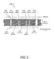
- FIG. 2illustrates an expanded view of a Detail A of FIG. 1 .
- Detail A of FIG. 2shows a portion of a single circuit row 22 , e.g., a circuit row 22 a , that includes a sampling of logic cells 24 , e.g., logic cells 24 a through 24 e , and a sampling of filler cells 26 , e.g., filler cells 26 a through 26 f .
- filler cell 26 a and 26 bare arranged on opposite boundaries of logic cell 24 a
- filler cell 26 b and 26 care arranged on opposite boundaries of logic cell 24 b
- filler cell 26 c and 26 dare arranged on opposite boundaries of logic cell 24 c
- filler cell 26 d and 26 eare arranged on opposite boundaries of logic cell 24 d
- filler cell 26 e and 26 fare arranged on opposite boundaries of logic cell 24 e.
- FIG. 2shows that each filler cell 26 is a certain number of TRACKS in width.
- the width of one TRACKcorrelates arbitrarily to the width of one wiring track for any given semiconductor technology.
- one TRACK in FIG. 2represents a wiring track width of 1.8 microns.
- Detail A of FIG. 2shows, for example, that filler cell 26 a is two TRACKS in width, filler cells 26 b , 26 c , 26 d , and 26 e are one TRACK in width, and filler cell 26 f is three TRACKS in width.
- the minimum spacing that is required between any two logic cells 24is, for example, four TRACKS in order to implement a customizable filler cell 28 , it is observed in FIG. 2 that no spacing between any two logic cells 24 meets this requirement. Details of a method of shifting slightly the positions of logic cells 24 in order to produce a customizable filler cell 28 are provided with reference to FIGS. 3A , 3 B, and 3 C.
- FIG. 3Aillustrates Detail A of FIGS. 1 and 2 that is modified to show a first exemplary step of a logic cell position adjustment operation.
- Detail A of FIG. 3Ashows that the position of logic cell 24 d within circuit row 22 a is shifted one TRACK toward second edge 32 of circuit layout 20 .
- filler cell 26 e that is shown in Detail A of FIG. 2is eliminated and filler cell 26 d that is shown in Detail A of FIG. 2 is increased in width from one to two TRACKS.
- FIG. 3Billustrates Detail A of FIGS. 1 and 2 that is modified to show a second exemplary step of a logic cell position adjustment operation.
- Detail A of FIG. 3Bshows that the position of logic cell 24 c within circuit row 22 a is shifted two TRACKS toward second edge 32 of circuit layout 20 .
- filler cell 26 d that is shown in Detail A of FIG. 3Ais eliminated and filler cell 26 c that is shown in Detail A of FIG. 3A is increased in width from one to three TRACKS.
- FIG. 3Cillustrates Detail A of FIGS. 1 and 2 that is modified to show a third exemplary step of a logic cell position adjustment operation.
- Detail A of FIG. 3Cshows that the position of logic cell 24 b within circuit row 22 a is shifted three TRACKS toward second edge 32 of circuit layout 20 .
- filler cell 26 c that is shown in Detail A of FIG. 3Bis eliminated and filler cell 26 b that is shown in Detail A of FIG. 3B is increased in width from one to four TRACKS.
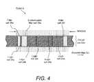
- FIG. 4illustrates Detail A that shows a customizable filler cell 28 , which is the result of the operations described in FIGS. 3A , 3 B, and 3 C. More specifically, if, for example, it is pre-established that a filler cell 26 must be at least four TRACKS in width in order be classified as a customizable filler cell 28 , filler cell 26 b that is shown in Detail A of FIG. 3C is reclassified as a customizable filler cell 28 a. Therefore, as a result of the operations that are described in FIGS. 3A , 3 B, and 3 C, circuit row 22 a of Detail A of FIG.
- FIGS. 3A , 3 B, and 3 CMore details of an algorithm that performs the logic cell position adjustment operation, as described in FIGS. 3A , 3 B, and 3 C, are described with reference to FIGS. 5 and 6 .
- FIG. 5illustrates a circuit layout 20 ′ that is the result of executing a filler cell placement method on circuit layout 20 of FIG. 1 , in accordance with the disclosure.
- a filler cell placement algorithmthat performs a comprehensive operation to adjust the positions of filler cells 26 of all circuit rows 22 in order to increase the instances of customizable filler cell 28 and to optimize the distribution and placement thereof is executed on a circuit layout, such as circuit layout 20 of FIG. 1 .
- An exemplary resultsuch as illustrated by circuit layout 20 ′ of FIG. 5 , shows the addition of multiple customizable filler cells 28 as compared with circuit layout 20 of FIG. 1 .
- FIG. 5shows an improved distribution of customizable filler cells 28 across the entire area of circuit layout 20 ′ of FIG. 5 , as compared with circuit layout 20 of FIG. 1 .
- a filler cell placement algorithm of the present inventionperforms an iterative process that is executable within any standard EDA application, such as Cadence, which performs standard place and route operations that are associated with an integrated circuit physical design process.
- Cadencewhich performs standard place and route operations that are associated with an integrated circuit physical design process.
- the operations of the filler cell placement algorithminclude, but are not limited to, the following.
- Example parametersmay include, but are not limited to, the following.
- this parameteris set to first edge 30 , second edge 32 , third edge 34 , fourth edge 36 , center of circuit layout 20 , or a specific circuit row 22 ;
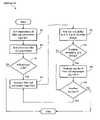
- FIG. 6illustrates a method 50 of optimizing customizable filler cells 28 in an integrated circuit physical design process by use of the filler cell placement method of the present invention.
- method 50 of the present inventionprovides a way of optimizing the locations, number, and distribution of customizable filler cells 28 in an integrated circuit physical design process, in order to maximize the opportunity for implementing circuit modifications.
- Method 50includes, but is not limited to, the following steps.
- Step 52the parameters of the filler cell placement algorithm, as described in FIG. 5 , are set.
- Method 50proceeds to step 54 .
- step 54after executing a synthesis operation on a given integrated circuit design, the initial configuration of customizable filler cells 28 and is analyzed. For example, after the synthesis operation, the placement of customizable filler cells 28 within each circuit row 22 of circuit layout 20 of FIG. 1 is analyzed in order to determine whether the location, number, and/or distribution of customizable filler cells 28 is adequate based, for example, on the size and complexity of the circuit design. Additionally, the analysis of step 54 may include determining whether additional customizable filler cells 28 are achievable by, for example, determining whether there are sufficient filler cells 26 to combine. Alternatively, based on x-y position only, it is determined whether the position of existing customizable filler cells 28 is satisfactory or whether it is beneficial to form customizable filler cells 28 at more strategic positions within circuit layout 20 . Method 50 proceeds to step 56 .
- step 56based on the analysis of step 54 , it is determined whether the positions of logic cells 24 of a given design require adjustment, in order to better optimize customizable filler cells 28 . If yes, method 50 proceeds to step 58 . If no, method 50 ends.
- the filler cell placement methodis executed within any standard EDA application, such as Cadence, which performs standard place and route operations that are associated with an integrated circuit physical design process. In doing so, the positions of logic cells 24 are adjusted in order to form customizable filler cells 28 , such as described in reference to FIGS. 3A , 3 B, and 3 C. Method 50 proceeds to step 60 .
- step 60the wireability and timing of the modified integrated circuit design, such as circuit layout 20 ′ of FIG. 5 , is verified.
- a routing algorithm and a timing analysis algorithm of the EDA applicationis executed in order to verify wireability and timing, respectively, of the modified integrated circuit design.
- Method 50proceeds to step 62 .
- step 62based on the results of step 60 , it is determined whether the wireability and timing of the modified integrated circuit design is satisfactory. If yes, method 50 proceeds to step 64 . If no, method 50 proceeds to step 66 .
- the results of filler cell placement algorithmare analyzed in order to determine whether the locations, number, and distribution of the resulting customizable filler cells 28 are satisfactory. For example, this determination may be via a manual inspection operation or via an automated operation that utilizes any user-defined criterion.
- Example automated operationsinclude, but are not limited to, calculating a percent increase in customizable filler cells 28 , analyzing the x-y position of the resulting customizable filler cells 28 , or calculating the number of customizable filler cells 28 per circuit row/column.
- step 66based on the results of step 60 or 64 , it is determined whether another iteration of the filler cell placement algorithm is required. If yes, method 50 returns to step 58 . If no, method 50 ends.
Landscapes
- Engineering & Computer Science (AREA)
- Computer Hardware Design (AREA)
- Physics & Mathematics (AREA)
- Theoretical Computer Science (AREA)
- Architecture (AREA)
- Evolutionary Computation (AREA)
- Geometry (AREA)
- General Engineering & Computer Science (AREA)
- General Physics & Mathematics (AREA)
- Design And Manufacture Of Integrated Circuits (AREA)
Abstract
Description
- 1. selecting a starting point within a given circuit layout, such as selecting a starting point near a particular edge or near the center of
circuit layout 20; - 2. selecting a direction in which the position of
logic cells 24 is adjusted, such as from one edge toward an opposite edge ofcircuit layout 20, from the perimeter edges ofcircuit layout 20 toward its center, or from the center ofcircuit layout 20 toward its perimeter edges; - 3. adjusting in the selected direction the position of
logic cells 24 and, thereby, combinefiller cells 26 in order to increase the accumulated area thereof, - 4. suspending the adjustment operation when a customizable filler cell28 is formed; and
- 5. resuming the adjustment operation from the point of the newly formed customizable filler cell28.
- 1. selecting a starting point within a given circuit layout, such as selecting a starting point near a particular edge or near the center of
- 1. Filler cell target size—for a given semiconductor technology, this parameter establishes the minimum filler cell size that may be classified as a customizable filler cell28. For example, this parameter may be set to 4, 8, 12 or 16 TRACKS;
- 2. Adjustment parameter—this parameter sets the adjustment direction of
logic cells 24 withincircuit layout 20. For example, for each circuit row22 this parameter is set tosecond edge 32 towardfourth edge 36 only,fourth edge 36 towardsecond edge 32 only, or bothsecond edge 32 andfourth edge 36 toward the center. Alternatively, forcircuit layout 20 this parameter is set to one circuit row22 to an adjacent circuit row22 in any desired direction; - 3. Starting point—this parameter sets the point from which to initiate the adjustment operation.
- 4. Maximum shift—this parameter sets the maximum amount of shift that is allowed for any
individual logic cell 24. For example, for a filler cell target size of 4 TRACKS this parameter is set to 3, for a filler cell target size of 8 TRACKS this parameter is set to 7, for a filler cell target size of 12 TRACKS this parameter is set to 11, or for a filler cell target size of 16 TRACKS this parameter is set to 15; - 5. Excluded areas—this parameter is set to identify critical areas to avoid within
circuit layout 20, such as certain critical circuit rows/columns or portions thereof; and - 6. Focus areas—this parameter is set to identify strategic areas within
circuit layout 20 near which customizable filler cells28 are most desired, such as certain strategic circuit rows/columns or portions thereof.
- 4. Maximum shift—this parameter sets the maximum amount of shift that is allowed for any
Claims (20)
Priority Applications (1)
| Application Number | Priority Date | Filing Date | Title |
|---|---|---|---|
| US11/427,719US7444609B2 (en) | 2006-06-29 | 2006-06-29 | Method of optimizing customizable filler cells in an integrated circuit physical design process |
Applications Claiming Priority (1)
| Application Number | Priority Date | Filing Date | Title |
|---|---|---|---|
| US11/427,719US7444609B2 (en) | 2006-06-29 | 2006-06-29 | Method of optimizing customizable filler cells in an integrated circuit physical design process |
Publications (2)
| Publication Number | Publication Date |
|---|---|
| US20080005712A1 US20080005712A1 (en) | 2008-01-03 |
| US7444609B2true US7444609B2 (en) | 2008-10-28 |
Family
ID=38878380
Family Applications (1)
| Application Number | Title | Priority Date | Filing Date |
|---|---|---|---|
| US11/427,719Active2027-01-06US7444609B2 (en) | 2006-06-29 | 2006-06-29 | Method of optimizing customizable filler cells in an integrated circuit physical design process |
Country Status (1)
| Country | Link |
|---|---|
| US (1) | US7444609B2 (en) |
Cited By (36)
| Publication number | Priority date | Publication date | Assignee | Title |
|---|---|---|---|---|
| US20080320430A1 (en)* | 2007-06-25 | 2008-12-25 | International Business Machines Corporation | Spare Gate Array Cell Distribution Analysis |
| US20090013297A1 (en)* | 2006-05-24 | 2009-01-08 | Texas Instruments Incorporated | Contact resistance and capacitance for semiconductor devices |
| US20100187627A1 (en)* | 2008-03-13 | 2010-07-29 | Tela Innovations, Inc. | Channelized Gate Level Cross-Coupled Transistor Device with Overlapping PMOS Transistors and Overlapping NMOS Transistors Relative to Direction of Gate Electrodes |
| US7842975B2 (en) | 2006-03-09 | 2010-11-30 | Tela Innovations, Inc. | Dynamic array architecture |
| US7888705B2 (en) | 2007-08-02 | 2011-02-15 | Tela Innovations, Inc. | Methods for defining dynamic array section with manufacturing assurance halo and apparatus implementing the same |
| US20110072407A1 (en)* | 2009-09-18 | 2011-03-24 | International Business Machines Corporation | Automatic Positioning of Gate Array Circuits in an Integrated Circuit Design |
| US7932545B2 (en) | 2006-03-09 | 2011-04-26 | Tela Innovations, Inc. | Semiconductor device and associated layouts including gate electrode level region having arrangement of six linear conductive segments with side-to-side spacing less than 360 nanometers |
| US7939443B2 (en) | 2008-03-27 | 2011-05-10 | Tela Innovations, Inc. | Methods for multi-wire routing and apparatus implementing same |
| US7943967B2 (en) | 2006-03-09 | 2011-05-17 | Tela Innovations, Inc. | Semiconductor device and associated layouts including diffusion contact placement restriction based on relation to linear conductive segments |
| US7979829B2 (en) | 2007-02-20 | 2011-07-12 | Tela Innovations, Inc. | Integrated circuit cell library with cell-level process compensation technique (PCT) application and associated methods |
| US20110167629A1 (en)* | 2004-12-31 | 2011-07-14 | Stmicroelectronics Pvt. Ltd. | Area-efficient distributed device structure for integrated voltage regulators |
| US7994545B2 (en) | 2007-10-26 | 2011-08-09 | Tela Innovations, Inc. | Methods, structures, and designs for self-aligning local interconnects used in integrated circuits |
| US8214778B2 (en) | 2007-08-02 | 2012-07-03 | Tela Innovations, Inc. | Methods for cell phasing and placement in dynamic array architecture and implementation of the same |
| US8225261B2 (en) | 2006-03-09 | 2012-07-17 | Tela Innovations, Inc. | Methods for defining contact grid in dynamic array architecture |
| US8225239B2 (en) | 2006-03-09 | 2012-07-17 | Tela Innovations, Inc. | Methods for defining and utilizing sub-resolution features in linear topology |
| US8245180B2 (en) | 2006-03-09 | 2012-08-14 | Tela Innovations, Inc. | Methods for defining and using co-optimized nanopatterns for integrated circuit design and apparatus implementing same |
| US8247846B2 (en) | 2006-03-09 | 2012-08-21 | Tela Innovations, Inc. | Oversized contacts and vias in semiconductor chip defined by linearly constrained topology |
| US20120246601A1 (en)* | 2011-03-23 | 2012-09-27 | Masanari Kajiwara | Pattern correcting method, mask forming method, and method of manufacturing semiconductor device |
| US8286107B2 (en) | 2007-02-20 | 2012-10-09 | Tela Innovations, Inc. | Methods and systems for process compensation technique acceleration |
| US8448102B2 (en) | 2006-03-09 | 2013-05-21 | Tela Innovations, Inc. | Optimizing layout of irregular structures in regular layout context |
| US8453094B2 (en) | 2008-01-31 | 2013-05-28 | Tela Innovations, Inc. | Enforcement of semiconductor structure regularity for localized transistors and interconnect |
| US8541879B2 (en) | 2007-12-13 | 2013-09-24 | Tela Innovations, Inc. | Super-self-aligned contacts and method for making the same |
| US8653857B2 (en) | 2006-03-09 | 2014-02-18 | Tela Innovations, Inc. | Circuitry and layouts for XOR and XNOR logic |
| US8661392B2 (en) | 2009-10-13 | 2014-02-25 | Tela Innovations, Inc. | Methods for cell boundary encroachment and layouts implementing the Same |
| US8658542B2 (en) | 2006-03-09 | 2014-02-25 | Tela Innovations, Inc. | Coarse grid design methods and structures |
| US8667443B2 (en) | 2007-03-05 | 2014-03-04 | Tela Innovations, Inc. | Integrated circuit cell library for multiple patterning |
| US8839175B2 (en) | 2006-03-09 | 2014-09-16 | Tela Innovations, Inc. | Scalable meta-data objects |
| US8863063B2 (en) | 2009-05-06 | 2014-10-14 | Tela Innovations, Inc. | Finfet transistor circuit |
| US9035359B2 (en) | 2006-03-09 | 2015-05-19 | Tela Innovations, Inc. | Semiconductor chip including region including linear-shaped conductive structures forming gate electrodes and having electrical connection areas arranged relative to inner region between transistors of different types and associated methods |
| US9122832B2 (en) | 2008-08-01 | 2015-09-01 | Tela Innovations, Inc. | Methods for controlling microloading variation in semiconductor wafer layout and fabrication |
| US9159627B2 (en) | 2010-11-12 | 2015-10-13 | Tela Innovations, Inc. | Methods for linewidth modification and apparatus implementing the same |
| US9230910B2 (en) | 2006-03-09 | 2016-01-05 | Tela Innovations, Inc. | Oversized contacts and vias in layout defined by linearly constrained topology |
| US9563733B2 (en) | 2009-05-06 | 2017-02-07 | Tela Innovations, Inc. | Cell circuit and layout with linear finfet structures |
| US10540471B2 (en) | 2016-05-11 | 2020-01-21 | Samsung Electronics Co., Ltd. | Layout design system and semiconductor device fabricated using the same |
| US10817640B2 (en) | 2018-11-09 | 2020-10-27 | Samsung Electronics Co., Ltd. | Integrated circuit including different types of cells, and method and system of designing the same |
| US20220405454A1 (en)* | 2021-06-16 | 2022-12-22 | International Business Machines Corporation | Filler cells for integrated circuit design |
Families Citing this family (9)
| Publication number | Priority date | Publication date | Assignee | Title |
|---|---|---|---|---|
| US7315631B1 (en)* | 2006-08-11 | 2008-01-01 | Fotonation Vision Limited | Real-time face tracking in a digital image acquisition device |
| US7895548B2 (en)* | 2007-10-26 | 2011-02-22 | Synopsys, Inc. | Filler cells for design optimization in a place-and-route system |
| US9472423B2 (en)* | 2007-10-30 | 2016-10-18 | Synopsys, Inc. | Method for suppressing lattice defects in a semiconductor substrate |
| US8266566B2 (en)* | 2010-09-10 | 2012-09-11 | International Business Machines Corporation | Stability-dependent spare cell insertion |
| US9213791B1 (en)* | 2014-07-17 | 2015-12-15 | Freescale Semiconductor, Inc. | Method and apparatus for abutting p-cell layout based on position and orientation |
| US9799575B2 (en)* | 2015-12-16 | 2017-10-24 | Pdf Solutions, Inc. | Integrated circuit containing DOEs of NCEM-enabled fill cells |
| US9946829B2 (en) | 2015-02-09 | 2018-04-17 | Mediatek Inc. | Methods for redistributing cell densities in layout area of IC |
| WO2021221651A1 (en)* | 2020-04-30 | 2021-11-04 | Siemens Industry Software Inc. | Correct-by-construction filler cell insertion |
| CN113515915B (en)* | 2021-04-23 | 2023-04-25 | 成都海光集成电路设计有限公司 | Method, device, equipment and storage medium for inserting filling unit |
Citations (10)
| Publication number | Priority date | Publication date | Assignee | Title |
|---|---|---|---|---|
| US6321371B1 (en) | 1999-07-01 | 2001-11-20 | Agilent Technologies, Inc. | Insertion of spare logic gates into the unused spaces between individual gates in standard cell artwork |
| US6446248B1 (en) | 2000-01-28 | 2002-09-03 | Lsi Logic Corporation | Spare cells placement methodology |
| US6470476B2 (en) | 2001-03-16 | 2002-10-22 | International Business Machines Corporation | Substitution of non-minimum groundrule cells for non-critical minimum groundrule cells to increase yield |
| US6557145B2 (en) | 1998-02-11 | 2003-04-29 | Monterey Design Systems, Inc. | Method for design optimization using logical and physical information |
| US20030233625A1 (en) | 2002-06-18 | 2003-12-18 | Ip-First, Llc. | Method for allocating spare cells in auto-place-route blocks |
| US6748579B2 (en) | 2002-08-30 | 2004-06-08 | Lsi Logic Corporation | Method of using filler metal for implementing changes in an integrated circuit design |
| US20040133868A1 (en) | 2002-11-05 | 2004-07-08 | Junji Ichimiya | Layout design method for semiconductor integrated circuit, and semiconductor integrated circuit |
| US20040199879A1 (en) | 2003-04-04 | 2004-10-07 | Bradfield Travis Alister | System and method for achieving timing closure in fixed placed designs after implementing logic changes |
| US20050039153A1 (en) | 2000-03-15 | 2005-02-17 | International Business Machines Corporation | Macro design techniques to accommodate chip level wiring and circuit placement across the macro |
| US20070124714A1 (en)* | 2005-07-14 | 2007-05-31 | Renesas Technology Corp. | Method for designing semiconductor integrated circuit layout |
- 2006
- 2006-06-29USUS11/427,719patent/US7444609B2/enactiveActive
Patent Citations (10)
| Publication number | Priority date | Publication date | Assignee | Title |
|---|---|---|---|---|
| US6557145B2 (en) | 1998-02-11 | 2003-04-29 | Monterey Design Systems, Inc. | Method for design optimization using logical and physical information |
| US6321371B1 (en) | 1999-07-01 | 2001-11-20 | Agilent Technologies, Inc. | Insertion of spare logic gates into the unused spaces between individual gates in standard cell artwork |
| US6446248B1 (en) | 2000-01-28 | 2002-09-03 | Lsi Logic Corporation | Spare cells placement methodology |
| US20050039153A1 (en) | 2000-03-15 | 2005-02-17 | International Business Machines Corporation | Macro design techniques to accommodate chip level wiring and circuit placement across the macro |
| US6470476B2 (en) | 2001-03-16 | 2002-10-22 | International Business Machines Corporation | Substitution of non-minimum groundrule cells for non-critical minimum groundrule cells to increase yield |
| US20030233625A1 (en) | 2002-06-18 | 2003-12-18 | Ip-First, Llc. | Method for allocating spare cells in auto-place-route blocks |
| US6748579B2 (en) | 2002-08-30 | 2004-06-08 | Lsi Logic Corporation | Method of using filler metal for implementing changes in an integrated circuit design |
| US20040133868A1 (en) | 2002-11-05 | 2004-07-08 | Junji Ichimiya | Layout design method for semiconductor integrated circuit, and semiconductor integrated circuit |
| US20040199879A1 (en) | 2003-04-04 | 2004-10-07 | Bradfield Travis Alister | System and method for achieving timing closure in fixed placed designs after implementing logic changes |
| US20070124714A1 (en)* | 2005-07-14 | 2007-05-31 | Renesas Technology Corp. | Method for designing semiconductor integrated circuit layout |
Cited By (207)
| Publication number | Priority date | Publication date | Assignee | Title |
|---|---|---|---|---|
| US20110167629A1 (en)* | 2004-12-31 | 2011-07-14 | Stmicroelectronics Pvt. Ltd. | Area-efficient distributed device structure for integrated voltage regulators |
| US9018046B2 (en) | 2004-12-31 | 2015-04-28 | Stmicroelectronics International N.V. | Area-efficient distributed device structure for integrated voltage regulators |
| US8426924B2 (en)* | 2004-12-31 | 2013-04-23 | Stmicroelectronics Pvt. Ltd. | Area-efficient distributed device structure for integrated voltage regulators |
| US8225239B2 (en) | 2006-03-09 | 2012-07-17 | Tela Innovations, Inc. | Methods for defining and utilizing sub-resolution features in linear topology |
| US8247846B2 (en) | 2006-03-09 | 2012-08-21 | Tela Innovations, Inc. | Oversized contacts and vias in semiconductor chip defined by linearly constrained topology |
| US8823062B2 (en) | 2006-03-09 | 2014-09-02 | Tela Innovations, Inc. | Integrated circuit with offset line end spacings in linear gate electrode level |
| US8921896B2 (en) | 2006-03-09 | 2014-12-30 | Tela Innovations, Inc. | Integrated circuit including linear gate electrode structures having different extension distances beyond contact |
| US8921897B2 (en) | 2006-03-09 | 2014-12-30 | Tela Innovations, Inc. | Integrated circuit with gate electrode conductive structures having offset ends |
| US8946781B2 (en) | 2006-03-09 | 2015-02-03 | Tela Innovations, Inc. | Integrated circuit including gate electrode conductive structures with different extension distances beyond contact |
| US8952425B2 (en) | 2006-03-09 | 2015-02-10 | Tela Innovations, Inc. | Integrated circuit including at least four linear-shaped conductive structures having extending portions of different length |
| US9009641B2 (en) | 2006-03-09 | 2015-04-14 | Tela Innovations, Inc. | Circuits with linear finfet structures |
| US7906801B2 (en) | 2006-03-09 | 2011-03-15 | Tela Innovations, Inc. | Semiconductor device and associated layouts having transistors formed from six linear conductive segments with intervening diffusion contact restrictions |
| US7923757B2 (en) | 2006-03-09 | 2011-04-12 | Tela Innovations, Inc. | Semiconductor device and associated layouts having linear shaped gate electrodes defined along at least five adjacent gate electrode tracks of equal pitch with gate electrode connection through single interconnect level |
| US7932545B2 (en) | 2006-03-09 | 2011-04-26 | Tela Innovations, Inc. | Semiconductor device and associated layouts including gate electrode level region having arrangement of six linear conductive segments with side-to-side spacing less than 360 nanometers |
| US7932544B2 (en) | 2006-03-09 | 2011-04-26 | Tela Innovations, Inc. | Semiconductor device and associated layouts including linear conductive segments having non-gate extension portions |
| US10230377B2 (en) | 2006-03-09 | 2019-03-12 | Tela Innovations, Inc. | Circuitry and layouts for XOR and XNOR logic |
| US7943967B2 (en) | 2006-03-09 | 2011-05-17 | Tela Innovations, Inc. | Semiconductor device and associated layouts including diffusion contact placement restriction based on relation to linear conductive segments |
| US7943966B2 (en) | 2006-03-09 | 2011-05-17 | Tela Innovations, Inc. | Integrated circuit and associated layout with gate electrode level portion including at least two complimentary transistor forming linear conductive segments and at least one non-gate linear conductive segment |
| US7948013B2 (en) | 2006-03-09 | 2011-05-24 | Tela Innovations, Inc. | Semiconductor device and associated layouts having linear shaped gate electrodes defined along at least five adjacent gate electrode tracks of equal pitch |
| US7948012B2 (en) | 2006-03-09 | 2011-05-24 | Tela Innovations, Inc. | Semiconductor device having 1965 nm gate electrode level region including at least four active linear conductive segments and at least one non-gate linear conductive segment |
| US7952119B2 (en) | 2006-03-09 | 2011-05-31 | Tela Innovations, Inc. | Semiconductor device and associated layout having three or more linear-shaped gate electrode level conductive segments of both equal length and equal pitch |
| US10217763B2 (en) | 2006-03-09 | 2019-02-26 | Tela Innovations, Inc. | Semiconductor chip having region including gate electrode features of rectangular shape on gate horizontal grid and first-metal structures of rectangular shape on at least eight first-metal gridlines of first-metal vertical grid |
| US9035359B2 (en) | 2006-03-09 | 2015-05-19 | Tela Innovations, Inc. | Semiconductor chip including region including linear-shaped conductive structures forming gate electrodes and having electrical connection areas arranged relative to inner region between transistors of different types and associated methods |
| US7910958B2 (en) | 2006-03-09 | 2011-03-22 | Tela Innovations, Inc. | Semiconductor device and associated layouts having transistors formed from linear conductive segment with non-active neighboring linear conductive segment |
| US7989848B2 (en) | 2006-03-09 | 2011-08-02 | Tela Innovations, Inc. | Semiconductor device having at least four side-by-side electrodes of equal length and equal pitch with at least two transistor connections to power or ground |
| US7989847B2 (en) | 2006-03-09 | 2011-08-02 | Tela Innovations, Inc. | Semiconductor device having linear-shaped gate electrodes of different transistor types with uniformity extending portions of different lengths |
| US9230910B2 (en) | 2006-03-09 | 2016-01-05 | Tela Innovations, Inc. | Oversized contacts and vias in layout defined by linearly constrained topology |
| US8022441B2 (en) | 2006-03-09 | 2011-09-20 | Tela Innovations, Inc. | Semiconductor device and associated layouts having transistors formed from six linear conductive segments with gate electrode-to-gate electrode connection through single interconnect level and common node connection through different interconnect level |
| US8030689B2 (en) | 2006-03-09 | 2011-10-04 | Tela Innovations, Inc. | Integrated circuit device and associated layout including separated diffusion regions of different type each having four gate electrodes with each of two complementary gate electrode pairs formed from respective linear conductive segment |
| US8035133B2 (en) | 2006-03-09 | 2011-10-11 | Tela Innovations, Inc. | Semiconductor device having two pairs of transistors of different types formed from shared linear-shaped conductive features with intervening transistors of common type on equal pitch |
| US10186523B2 (en) | 2006-03-09 | 2019-01-22 | Tela Innovations, Inc. | Semiconductor chip having region including gate electrode features formed in part from rectangular layout shapes on gate horizontal grid and first-metal structures formed in part from rectangular layout shapes on at least eight first-metal gridlines of first-metal vertical grid |
| US8058671B2 (en) | 2006-03-09 | 2011-11-15 | Tela Innovations, Inc. | Semiconductor device having at least three linear-shaped electrode level conductive features of equal length positioned side-by-side at equal pitch |
| US8072003B2 (en) | 2006-03-09 | 2011-12-06 | Tela Innovations, Inc. | Integrated circuit device and associated layout including two pairs of co-aligned complementary gate electrodes with offset gate contact structures |
| US8089102B2 (en) | 2006-03-09 | 2012-01-03 | Tela Innovations, Inc. | Method for fabricating integrated circuit having three or more linear-shaped gate electrode level conductive segments of both equal length and equal pitch |
| US8088680B2 (en) | 2006-03-09 | 2012-01-03 | Tela Innovations, Inc. | Method for fabricating integrated circuit having at least three linear-shaped gate electrode level conductive features of equal length positioned side-by-side at equal pitch |
| US8253172B2 (en) | 2006-03-09 | 2012-08-28 | Tela Innovations, Inc. | Semiconductor device with linearly restricted gate level region including four serially connected transistors of first type and four serially connected transistors of second type separated by non-diffusion region |
| US8088682B2 (en) | 2006-03-09 | 2012-01-03 | Tela Innovations, Inc. | Method for fabricating integrated circuit with gate electrode level region including two side-by-side ones of at least three linear-shaped conductive structures electrically connected to each other through non-gate level |
| US8089100B2 (en) | 2006-03-09 | 2012-01-03 | Tela Innovations, Inc. | Integrated circuit with gate electrode level region including at least four linear-shaped conductive structures forming gate electrodes of transistors and including extending portions of at least two different sizes |
| US8089101B2 (en) | 2006-03-09 | 2012-01-03 | Tela Innovations, Inc. | Integrated circuit device with gate electrode level region including two side-by-side ones of at least three linear-shaped conductive structures electrically connected to each other through non-gate level |
| US8089104B2 (en) | 2006-03-09 | 2012-01-03 | Tela Innovations, Inc. | Integrated circuit with gate electrode level region including multiple linear-shaped conductive structures forming gate electrodes of transistors and including uniformity extending portions of different size |
| US8088679B2 (en) | 2006-03-09 | 2012-01-03 | Tela Innovations, Inc. | Method for fabricating integrated circuit with gate electrode level portion including at least two complementary transistor forming linear conductive segments and at least one non-gate linear conductive segment |
| US8089103B2 (en) | 2006-03-09 | 2012-01-03 | Tela Innovations, Inc. | Integrated circuit device with gate level region including at least three linear-shaped conductive segments having offset line ends and forming three transistors of first type and one transistor of second type |
| US8088681B2 (en) | 2006-03-09 | 2012-01-03 | Tela Innovations, Inc. | Method for fabricating integrated circuit including separated diffusion regions of different type each having four gate electrodes with each of two complementary gate electrode pairs formed from respective linear condcutive segment |
| US8089099B2 (en) | 2006-03-09 | 2012-01-03 | Tela Innovations, Inc, | Integrated circuit device and associated layout including gate electrode level region of 965 NM radius with linear-shaped conductive segments on fixed pitch |
| US8101975B2 (en) | 2006-03-09 | 2012-01-24 | Tela Innovations, Inc. | Integrated circuit device with gate level region including non-gate linear conductive segment positioned within 965 nanometers of four transistors of first type and four transistors of second type |
| US9240413B2 (en) | 2006-03-09 | 2016-01-19 | Tela Innovations, Inc. | Methods, structures, and designs for self-aligning local interconnects used in integrated circuits |
| US8110854B2 (en) | 2006-03-09 | 2012-02-07 | Tela Innovations, Inc. | Integrated circuit device with linearly defined gate electrode level region and shared diffusion region of first type connected to shared diffusion region of second type through at least two interconnect levels |
| US8129751B2 (en) | 2006-03-09 | 2012-03-06 | Tela Innovations, Inc. | Integrated circuit including at least six linear-shaped conductive structures forming gate electrodes and including four conductive contacting structures having at least two different connection distances |
| US8129750B2 (en) | 2006-03-09 | 2012-03-06 | Tela Innovations, Inc. | Integrated circuit including at least six linear-shaped conductive structures forming gate electrodes of transistors with at least two linear-shaped conductive structures of different length |
| US8129819B2 (en) | 2006-03-09 | 2012-03-06 | Tela Innovations, Inc. | Method of fabricating integrated circuit including at least six linear-shaped conductive structures at equal pitch including at least two linear-shaped conductive structures having non-gate portions of different length |
| US8129756B2 (en) | 2006-03-09 | 2012-03-06 | Tela Innovations, Inc. | Integrated circuit including at least six linear-shaped conductive structures forming gate electrodes of transistors with at least two different extension distances beyond conductive contacting structures |
| US8129757B2 (en) | 2006-03-09 | 2012-03-06 | Tela Innovations, Inc. | Integrated circuit including at least six linear-shaped conductive structive structures at equal pitch including at least two linear-shaped conductive structures having non-gate portions of different length |
| US8129753B2 (en) | 2006-03-09 | 2012-03-06 | Tela Innovations, Inc. | Integrated circuit including gate electrode level region including at least seven linear-shaped conductive structures of equal length positioned at equal pitch with at least two linear-shaped conductive structures each forming one transistor and having extending portion sized greater than gate portion |
| US8129752B2 (en) | 2006-03-09 | 2012-03-06 | Tela Innovations, Inc. | Integrated circuit including a linear-shaped conductive structure forming one gate electrode and having length greater than or equal to one-half the length of linear-shaped conductive structure forming two gate electrodes |
| US8129755B2 (en) | 2006-03-09 | 2012-03-06 | Tela Innovations, Inc. | Integrated circuit with gate electrode level including at least four linear-shaped conductive structures of equal length and equal pitch with linear-shaped conductive structure forming one transistor |
| US8129754B2 (en) | 2006-03-09 | 2012-03-06 | Tela Innovations, Inc. | Integrated circuit with gate electrode level including at least six linear-shaped conductive structures forming gate electrodes of transisters with at least one pair of linear-shaped conductive structures having offset ends |
| US8134183B2 (en) | 2006-03-09 | 2012-03-13 | Tela Innovations, Inc. | Integrated circuit including linear-shaped conductive structures that have gate portions and extending portions of different size |
| US8134186B2 (en) | 2006-03-09 | 2012-03-13 | Tela Innovations, Inc. | Integrated circuit including at least three linear-shaped conductive structures at equal pitch including linear-shaped conductive structure having non-gate portion length greater than gate portion length |
| US8134185B2 (en) | 2006-03-09 | 2012-03-13 | Tela Innovations, Inc. | Integrated circuit having gate electrode level region including at least seven linear-shaped conductive structures at equal pitch including linear-shaped conductive structure forming transistors of two different types and at least three linear-shaped conductive structures having aligned ends |
| US8134184B2 (en) | 2006-03-09 | 2012-03-13 | Tela Innovations, Inc. | Integrated circuit having gate electrode level region including at least four linear-shaped conductive structures with some outer-contacted linear-shaped conductive structures having larger outer extending portion than inner extending portion |
| US8138525B2 (en) | 2006-03-09 | 2012-03-20 | Tela Innovations, Inc. | Integrated circuit including at least three linear-shaped conductive structures of different length each forming gate of different transistor |
| US8198656B2 (en) | 2006-03-09 | 2012-06-12 | Tela Innovations, Inc. | Integrated circuit including gate electrode level region including at least four linear-shaped conductive structures of equal length having aligned ends and positioned at equal pitch and forming multiple gate electrodes of transistors of different type |
| US8207053B2 (en) | 2006-03-09 | 2012-06-26 | Tela Innovations, Inc. | Electrodes of transistors with at least two linear-shaped conductive structures of different length |
| US9336344B2 (en) | 2006-03-09 | 2016-05-10 | Tela Innovations, Inc. | Coarse grid design methods and structures |
| US8217428B2 (en) | 2006-03-09 | 2012-07-10 | Tela Innovations, Inc. | Integrated circuit including gate electrode level region including at least three linear-shaped conductive structures of equal length having aligned ends and positioned at equal pitch and forming multiple gate electrodes of transistors of different type |
| US8225261B2 (en) | 2006-03-09 | 2012-07-17 | Tela Innovations, Inc. | Methods for defining contact grid in dynamic array architecture |
| US8839175B2 (en) | 2006-03-09 | 2014-09-16 | Tela Innovations, Inc. | Scalable meta-data objects |
| US8245180B2 (en) | 2006-03-09 | 2012-08-14 | Tela Innovations, Inc. | Methods for defining and using co-optimized nanopatterns for integrated circuit design and apparatus implementing same |
| US8658542B2 (en) | 2006-03-09 | 2014-02-25 | Tela Innovations, Inc. | Coarse grid design methods and structures |
| US8089098B2 (en) | 2006-03-09 | 2012-01-03 | Tela Innovations, Inc. | Integrated circuit device and associated layout including linear gate electrodes of different transistor types next to linear-shaped non-gate conductive segment |
| US8253173B2 (en) | 2006-03-09 | 2012-08-28 | Tela Innovations, Inc. | Semiconductor device with gate level including four transistors of first type and four transistors of second type separated by non-diffusion region and having at least two gate contacts positioned outside separating non-diffusion region |
| US8258551B2 (en) | 2006-03-09 | 2012-09-04 | Tela Innovations, Inc. | Semiconductor device with gate level including transistors of first type and transistors of second type with corresponding gate contact placement restriction |
| US8258548B2 (en) | 2006-03-09 | 2012-09-04 | Tela Innovations, Inc. | Semiconductor device with gate level including four transistors of first type and four transistors of second type separated by non-diffusion region with restricted gate contact placement over separating non-diffusion region |
| US8258547B2 (en) | 2006-03-09 | 2012-09-04 | Tela Innovations, Inc. | Semiconductor device with linearly restricted gate level region including two transistors of first type and two transistors of second type with offset gate contacts |
| US8258552B2 (en) | 2006-03-09 | 2012-09-04 | Tela Innovations, Inc. | Semiconductor device including at least six transistor forming linear shapes with at least two transistor forming linear shapes having offset ends |
| US8258549B2 (en) | 2006-03-09 | 2012-09-04 | Tela Innovations, Inc. | Semiconductor device including two transistors of first type having gates formed by conductors of different length respectively aligned with two transistors of second type having gates formed by conductors of different length |
| US8258550B2 (en) | 2006-03-09 | 2012-09-04 | Tela Innovations, Inc. | Semiconductor device including at least six transistor forming linear shapes including at least two transistor forming linear shapes having different extension distances beyond gate contact |
| US10141334B2 (en) | 2006-03-09 | 2018-11-27 | Tela Innovations, Inc. | Semiconductor chip including region having rectangular-shaped gate structures and first-metal structures |
| US10141335B2 (en) | 2006-03-09 | 2018-11-27 | Tela Innovations, Inc. | Semiconductor CIP including region having rectangular-shaped gate structures and first metal structures |
| US8264007B2 (en) | 2006-03-09 | 2012-09-11 | Tela Innovations, Inc. | Semiconductor device including at least six transistor forming linear shapes including at least two different gate contact connection distances |
| US8264009B2 (en) | 2006-03-09 | 2012-09-11 | Tela Innovations, Inc. | Semiconductor device with linearly restricted gate level region including four transistors of first type and four transistors of second type with gate defining shapes of different length |
| US9425273B2 (en) | 2006-03-09 | 2016-08-23 | Tela Innovations, Inc. | Semiconductor chip including integrated circuit including at least five gate level conductive structures having particular spatial and electrical relationship and method for manufacturing the same |
| US8264008B2 (en) | 2006-03-09 | 2012-09-11 | Tela Innovations, Inc. | Semiconductor device including transistor forming linear shapes including gate portions and extending portions of different size |
| US9917056B2 (en) | 2006-03-09 | 2018-03-13 | Tela Innovations, Inc. | Coarse grid design methods and structures |
| US8653857B2 (en) | 2006-03-09 | 2014-02-18 | Tela Innovations, Inc. | Circuitry and layouts for XOR and XNOR logic |
| US9905576B2 (en) | 2006-03-09 | 2018-02-27 | Tela Innovations, Inc. | Semiconductor chip including region having rectangular-shaped gate structures and first metal structures |
| US9425272B2 (en) | 2006-03-09 | 2016-08-23 | Tela Innovations, Inc. | Semiconductor chip including integrated circuit including four transistors of first transistor type and four transistors of second transistor type with electrical connections between various transistors and methods for manufacturing the same |
| US9425145B2 (en) | 2006-03-09 | 2016-08-23 | Tela Innovations, Inc. | Oversized contacts and vias in layout defined by linearly constrained topology |
| US9443947B2 (en) | 2006-03-09 | 2016-09-13 | Tela Innovations, Inc. | Semiconductor chip including region having integrated circuit transistor gate electrodes formed by various conductive structures of specified shape and position and method for manufacturing the same |
| US9859277B2 (en) | 2006-03-09 | 2018-01-02 | Tela Innovations, Inc. | Methods, structures, and designs for self-aligning local interconnects used in integrated circuits |
| US9589091B2 (en) | 2006-03-09 | 2017-03-07 | Tela Innovations, Inc. | Scalable meta-data objects |
| US9754878B2 (en) | 2006-03-09 | 2017-09-05 | Tela Innovations, Inc. | Semiconductor chip including a chip level based on a layout that includes both regular and irregular wires |
| US7910959B2 (en) | 2006-03-09 | 2011-03-22 | Tela Innovations, Inc. | Semiconductor device and associated layouts having transistors formed from six linear conductive segments with gate electrode connection through single interconnect level |
| US8436400B2 (en) | 2006-03-09 | 2013-05-07 | Tela Innovations, Inc. | Semiconductor device with gate level including gate electrode conductors for transistors of first type and transistors of second type with some gate electrode conductors of different length |
| US9741719B2 (en) | 2006-03-09 | 2017-08-22 | Tela Innovations, Inc. | Methods, structures, and designs for self-aligning local interconnects used in integrated circuits |
| US8448102B2 (en) | 2006-03-09 | 2013-05-21 | Tela Innovations, Inc. | Optimizing layout of irregular structures in regular layout context |
| US7842975B2 (en) | 2006-03-09 | 2010-11-30 | Tela Innovations, Inc. | Dynamic array architecture |
| US9711495B2 (en) | 2006-03-09 | 2017-07-18 | Tela Innovations, Inc. | Oversized contacts and vias in layout defined by linearly constrained topology |
| US9673825B2 (en) | 2006-03-09 | 2017-06-06 | Tela Innovations, Inc. | Circuitry and layouts for XOR and XNOR logic |
| US8112737B2 (en)* | 2006-05-24 | 2012-02-07 | Texas Instruments Incorporated | Contact resistance and capacitance for semiconductor devices |
| US20090013297A1 (en)* | 2006-05-24 | 2009-01-08 | Texas Instruments Incorporated | Contact resistance and capacitance for semiconductor devices |
| US7979829B2 (en) | 2007-02-20 | 2011-07-12 | Tela Innovations, Inc. | Integrated circuit cell library with cell-level process compensation technique (PCT) application and associated methods |
| US8286107B2 (en) | 2007-02-20 | 2012-10-09 | Tela Innovations, Inc. | Methods and systems for process compensation technique acceleration |
| US10074640B2 (en) | 2007-03-05 | 2018-09-11 | Tela Innovations, Inc. | Integrated circuit cell library for multiple patterning |
| US9633987B2 (en) | 2007-03-05 | 2017-04-25 | Tela Innovations, Inc. | Integrated circuit cell library for multiple patterning |
| US8667443B2 (en) | 2007-03-05 | 2014-03-04 | Tela Innovations, Inc. | Integrated circuit cell library for multiple patterning |
| US9424387B2 (en) | 2007-03-07 | 2016-08-23 | Tela Innovations, Inc. | Methods for cell phasing and placement in dynamic array architecture and implementation of the same |
| US8966424B2 (en) | 2007-03-07 | 2015-02-24 | Tela Innovations, Inc. | Methods for cell phasing and placement in dynamic array architecture and implementation of the same |
| US9595515B2 (en) | 2007-03-07 | 2017-03-14 | Tela Innovations, Inc. | Semiconductor chip including integrated circuit defined within dynamic array section |
| US9910950B2 (en) | 2007-03-07 | 2018-03-06 | Tela Innovations, Inc. | Methods for cell phasing and placement in dynamic array architecture and implementation of the same |
| US7676776B2 (en)* | 2007-06-25 | 2010-03-09 | International Business Machines Corporation | Spare gate array cell distribution analysis |
| US20080320430A1 (en)* | 2007-06-25 | 2008-12-25 | International Business Machines Corporation | Spare Gate Array Cell Distribution Analysis |
| US7908578B2 (en) | 2007-08-02 | 2011-03-15 | Tela Innovations, Inc. | Methods for designing semiconductor device with dynamic array section |
| US8283701B2 (en) | 2007-08-02 | 2012-10-09 | Tela Innovations, Inc. | Semiconductor device with dynamic array sections defined and placed according to manufacturing assurance halos |
| US8549455B2 (en) | 2007-08-02 | 2013-10-01 | Tela Innovations, Inc. | Methods for cell phasing and placement in dynamic array architecture and implementation of the same |
| US8214778B2 (en) | 2007-08-02 | 2012-07-03 | Tela Innovations, Inc. | Methods for cell phasing and placement in dynamic array architecture and implementation of the same |
| US8356268B2 (en) | 2007-08-02 | 2013-01-15 | Tela Innovations, Inc. | Integrated circuit device including dynamic array section with gate level having linear conductive features on at least three side-by-side lines and uniform line end spacings |
| US8759882B2 (en) | 2007-08-02 | 2014-06-24 | Tela Innovations, Inc. | Semiconductor device with dynamic array sections defined and placed according to manufacturing assurance halos |
| US7888705B2 (en) | 2007-08-02 | 2011-02-15 | Tela Innovations, Inc. | Methods for defining dynamic array section with manufacturing assurance halo and apparatus implementing the same |
| US7917879B2 (en) | 2007-08-02 | 2011-03-29 | Tela Innovations, Inc. | Semiconductor device with dynamic array section |
| US8756551B2 (en) | 2007-08-02 | 2014-06-17 | Tela Innovations, Inc. | Methods for designing semiconductor device with dynamic array section |
| US8680626B2 (en) | 2007-10-26 | 2014-03-25 | Tela Innovations, Inc. | Methods, structures, and designs for self-aligning local interconnects used in integrated circuits |
| US10734383B2 (en) | 2007-10-26 | 2020-08-04 | Tela Innovations, Inc. | Methods, structures, and designs for self-aligning local interconnects used in integrated circuits |
| US7994545B2 (en) | 2007-10-26 | 2011-08-09 | Tela Innovations, Inc. | Methods, structures, and designs for self-aligning local interconnects used in integrated circuits |
| US9281371B2 (en) | 2007-12-13 | 2016-03-08 | Tela Innovations, Inc. | Super-self-aligned contacts and method for making the same |
| US10461081B2 (en) | 2007-12-13 | 2019-10-29 | Tel Innovations, Inc. | Super-self-aligned contacts and method for making the same |
| US8951916B2 (en) | 2007-12-13 | 2015-02-10 | Tela Innovations, Inc. | Super-self-aligned contacts and method for making the same |
| US9818747B2 (en) | 2007-12-13 | 2017-11-14 | Tela Innovations, Inc. | Super-self-aligned contacts and method for making the same |
| US8541879B2 (en) | 2007-12-13 | 2013-09-24 | Tela Innovations, Inc. | Super-self-aligned contacts and method for making the same |
| US9202779B2 (en) | 2008-01-31 | 2015-12-01 | Tela Innovations, Inc. | Enforcement of semiconductor structure regularity for localized transistors and interconnect |
| US8701071B2 (en) | 2008-01-31 | 2014-04-15 | Tela Innovations, Inc. | Enforcement of semiconductor structure regularity for localized transistors and interconnect |
| US9530734B2 (en) | 2008-01-31 | 2016-12-27 | Tela Innovations, Inc. | Enforcement of semiconductor structure regularity for localized transistors and interconnect |
| US8453094B2 (en) | 2008-01-31 | 2013-05-28 | Tela Innovations, Inc. | Enforcement of semiconductor structure regularity for localized transistors and interconnect |
| US8558322B2 (en) | 2008-03-13 | 2013-10-15 | Tela Innovations, Inc. | Integrated circuit including cross-coupled transistors having gate electrodes formed within gate level feature layout channels with at least two gate electrodes electrically connected to each other through gate level feature |
| US8581303B2 (en) | 2008-03-13 | 2013-11-12 | Tela Innovations, Inc. | Integrated circuit including cross-coupled trasistors having gate electrodes formed within gate level feature layout channels with four inside positioned gate contacts having offset relationships and electrical connection of cross-coupled transistors through same interconnect layer |
| US8835989B2 (en) | 2008-03-13 | 2014-09-16 | Tela Innovations, Inc. | Integrated circuit including cross-coupled transistors having gate electrodes formed within gate level feature layout channels with gate electrode placement specifications |
| US8847331B2 (en) | 2008-03-13 | 2014-09-30 | Tela Innovations, Inc. | Semiconductor chip including region having cross-coupled transistor configuration with offset electrical connection areas on gate electrode forming conductive structures and at least two different inner extension distances of gate electrode forming conductive structures |
| US8847329B2 (en) | 2008-03-13 | 2014-09-30 | Tela Innovations, Inc. | Cross-coupled transistor circuit defined having diffusion regions of common node on opposing sides of same gate electrode track with at least two non-inner positioned gate contacts |
| US8853793B2 (en) | 2008-03-13 | 2014-10-07 | Tela Innovations, Inc. | Integrated circuit including gate electrode level region including cross-coupled transistors having gate contacts located over inner portion of gate electrode level region and offset gate level feature line ends |
| US8853794B2 (en) | 2008-03-13 | 2014-10-07 | Tela Innovations, Inc. | Integrated circuit within semiconductor chip including cross-coupled transistor configuration |
| US20100187627A1 (en)* | 2008-03-13 | 2010-07-29 | Tela Innovations, Inc. | Channelized Gate Level Cross-Coupled Transistor Device with Overlapping PMOS Transistors and Overlapping NMOS Transistors Relative to Direction of Gate Electrodes |
| US8866197B2 (en) | 2008-03-13 | 2014-10-21 | Tela Innovations, Inc. | Integrated circuit including cross-coupled transistors having gate electrodes formed within gate level feature layout channels with at least two gate electrodes electrically connected to each other through another transistor forming gate level feature |
| US8872283B2 (en) | 2008-03-13 | 2014-10-28 | Tela Innovations, Inc. | Integrated circuit including cross-coupled transistors having gate electrodes formed within gate level feature layout channels with shared diffusion regions on opposite sides of two-transistor-forming gate level feature |
| US8816402B2 (en) | 2008-03-13 | 2014-08-26 | Tela Innovations, Inc. | Integrated circuit including cross-coupled transistors having gate electrodes formed within gate level feature layout channels with gate level feature layout channel including single transistor |
| US8785979B2 (en) | 2008-03-13 | 2014-07-22 | Tela Innovations, Inc. | Integrated circuit including cross-coupled transistors having gate electrodes formed within gate level feature layout channels with two inside positioned gate contacts and two outside positioned gate contacts and electrical connection of cross-coupled transistors through same interconnect layer |
| US8785978B2 (en) | 2008-03-13 | 2014-07-22 | Tela Innovations, Inc. | Integrated circuit including cross-coupled transistors having gate electrodes formed within gate level feature layout channels with electrical connection of cross-coupled transistors through same interconnect layer |
| US8772839B2 (en) | 2008-03-13 | 2014-07-08 | Tela Innovations, Inc. | Integrated circuit including cross-coupled transistors having gate electrodes formed within gate level feature layout channels with four inside positioned gate contacts having offset and aligned relationships and electrical connection of transistor gates through linear interconnect conductors in single interconnect layer |
| US10727252B2 (en) | 2008-03-13 | 2020-07-28 | Tela Innovations, Inc. | Semiconductor chip including integrated circuit having cross-coupled transistor configuration and method for manufacturing the same |
| US8742462B2 (en) | 2008-03-13 | 2014-06-03 | Tela Innovations, Inc. | Integrated circuit including cross-coupled transistors having gate electrodes formed within gate level feature layout channels with gate contact position specifications |
| US8742463B2 (en) | 2008-03-13 | 2014-06-03 | Tela Innovations, Inc. | Integrated circuit including cross-coupled transistors having gate electrodes formed within gate level feature layout channels with outer positioned gate contacts |
| US8735944B2 (en) | 2008-03-13 | 2014-05-27 | Tela Innovations, Inc. | Integrated circuit including cross-coupled transistors having gate electrodes formed within gate level feature layout channels with serially connected transistors |
| US8735995B2 (en) | 2008-03-13 | 2014-05-27 | Tela Innovations, Inc. | Cross-coupled transistor circuit defined on three gate electrode tracks with diffusion regions of common node on opposing sides of same gate electrode track |
| US9081931B2 (en) | 2008-03-13 | 2015-07-14 | Tela Innovations, Inc. | Cross-coupled transistor circuit having diffusion regions of common node on opposing sides of same gate electrode track and gate node connection through single interconnect layer |
| US9117050B2 (en) | 2008-03-13 | 2015-08-25 | Tela Innovations, Inc. | Integrated circuit including cross-coupled transistors having gate electrodes formed within gate level feature layout channels with gate contact position and offset specifications |
| US10658385B2 (en) | 2008-03-13 | 2020-05-19 | Tela Innovations, Inc. | Cross-coupled transistor circuit defined on four gate electrode tracks |
| US10651200B2 (en) | 2008-03-13 | 2020-05-12 | Tela Innovations, Inc. | Cross-coupled transistor circuit defined on three gate electrode tracks |
| US8729643B2 (en) | 2008-03-13 | 2014-05-20 | Tela Innovations, Inc. | Cross-coupled transistor circuit including offset inner gate contacts |
| US9208279B2 (en) | 2008-03-13 | 2015-12-08 | Tela Innovations, Inc. | Semiconductor chip including digital logic circuit including linear-shaped conductive structures having electrical connection areas located within inner region between transistors of different type and associated methods |
| US9213792B2 (en) | 2008-03-13 | 2015-12-15 | Tela Innovations, Inc. | Semiconductor chip including digital logic circuit including at least six transistors with some transistors forming cross-coupled transistor configuration and associated methods |
| US8729606B2 (en) | 2008-03-13 | 2014-05-20 | Tela Innovations, Inc. | Integrated circuit including cross-coupled transistors having gate electrodes formed within gate level feature layout channels |
| US8680583B2 (en) | 2008-03-13 | 2014-03-25 | Tela Innovations, Inc. | Integrated circuit including cross-coupled transistors having gate electrodes formed within at least nine gate level feature layout channels |
| US9245081B2 (en) | 2008-03-13 | 2016-01-26 | Tela Innovations, Inc. | Semiconductor chip including digital logic circuit including at least nine linear-shaped conductive structures collectively forming gate electrodes of at least six transistors with some transistors forming cross-coupled transistor configuration and associated methods |
| US7956421B2 (en) | 2008-03-13 | 2011-06-07 | Tela Innovations, Inc. | Cross-coupled transistor layouts in restricted gate level layout architecture |
| US8669595B2 (en) | 2008-03-13 | 2014-03-11 | Tela Innovations, Inc. | Integrated circuit including cross-coupled transistors having gate electrodes formed within gate level feature layout channels with gate contact position, alignment, and offset specifications |
| US8669594B2 (en) | 2008-03-13 | 2014-03-11 | Tela Innovations, Inc. | Integrated circuit including cross-coupled transistors having gate electrodes formed within at least twelve gate level feature layout channels |
| US8058691B2 (en) | 2008-03-13 | 2011-11-15 | Tela Innovations, Inc. | Semiconductor device including cross-coupled transistors formed from linear-shaped gate level features |
| US8258581B2 (en) | 2008-03-13 | 2012-09-04 | Tela Innovations, Inc. | Integrated circuit including cross-coupled transistors with two transistors of different type formed by same gate level structure and two transistors of different type formed by separate gate level structures |
| US8592872B2 (en) | 2008-03-13 | 2013-11-26 | Tela Innovations, Inc. | Integrated circuit including cross-coupled transistors with two transistors of different type having gate electrodes formed by common gate level feature with shared diffusion regions on opposite sides of common gate level feature |
| US8587034B2 (en) | 2008-03-13 | 2013-11-19 | Tela Innovations, Inc. | Integrated circuit including cross-coupled transistors having gate electrodes formed within gate level feature layout channels with four inside positioned gate contacts and electrical connection of transistor gates through linear interconnect conductors in single interconnect layer |
| US8581304B2 (en) | 2008-03-13 | 2013-11-12 | Tela Innovations, Inc. | Integrated circuit including cross-coupled transistors having gate electrodes formed within gate level feature layout channels with four inside positioned gate contacts having offset and aligned relationships |
| US8836045B2 (en) | 2008-03-13 | 2014-09-16 | Tela Innovations, Inc. | Cross-coupled transistor circuit having diffusion regions of common node on opposing sides of same gate electrode track |
| US8575706B2 (en) | 2008-03-13 | 2013-11-05 | Tela Innovations, Inc. | Integrated circuit including cross-coupled transistors having gate electrodes formed within gate level feature layout channels with at least two different gate level features inner extensions beyond gate electrode |
| US8264049B2 (en) | 2008-03-13 | 2012-09-11 | Tela Innovations, Inc. | Integrated circuit including cross-coupled transistors with two transistors of different type having gate electrodes formed by common gate level feature with shared diffusion regions on opposite sides of common gate level feature |
| US9536899B2 (en) | 2008-03-13 | 2017-01-03 | Tela Innovations, Inc. | Semiconductor chip including integrated circuit having cross-coupled transistor configuration and method for manufacturing the same |
| US8264044B2 (en) | 2008-03-13 | 2012-09-11 | Tela Innovations, Inc. | Integrated circuit including cross-coupled transistors having two complementary pairs of co-aligned gate electrodes with offset contacting structures positioned between transistors of different type |
| US8569841B2 (en) | 2008-03-13 | 2013-10-29 | Tela Innovations, Inc. | Integrated circuit including cross-coupled transistors having gate electrodes formed within gate level feature layout channels with at least one gate level feature extending into adjacent gate level feature layout channel |
| US8564071B2 (en) | 2008-03-13 | 2013-10-22 | Tela Innovations, Inc. | Integrated circuit including cross-coupled transistors having gate electrodes formed within gate level feature layout channels with at least two different gate level feature extensions beyond contact |
| US8552509B2 (en) | 2008-03-13 | 2013-10-08 | Tela Innovations, Inc. | Integrated circuit including cross-coupled transistors having gate electrodes formed within gate level feature layout channels with other transistors positioned between cross-coupled transistors |
| US8552508B2 (en) | 2008-03-13 | 2013-10-08 | Tela Innovations, Inc. | Integrated circuit including cross-coupled transistors having gate electrodes formed within gate level feature layout channels with shared diffusion regions on opposite sides of two-transistor-forming gate level feature and electrical connection of transistor gates through linear interconnect conductors in single interconnect layer |
| US10020321B2 (en) | 2008-03-13 | 2018-07-10 | Tela Innovations, Inc. | Cross-coupled transistor circuit defined on two gate electrode tracks |
| US8274099B2 (en) | 2008-03-13 | 2012-09-25 | Tela Innovations, Inc. | Integrated circuit including cross-coupled transistors having gate electrodes formed within gate level feature layout channels with gate contact position and offset specifications |
| US9871056B2 (en) | 2008-03-13 | 2018-01-16 | Tela Innovations, Inc. | Semiconductor chip including integrated circuit having cross-coupled transistor configuration and method for manufacturing the same |
| US8405162B2 (en) | 2008-03-13 | 2013-03-26 | Tela Innovations, Inc. | Integrated circuit including gate electrode level region including cross-coupled transistors having at least one gate contact located over outer portion of gate electrode level region |
| US8395224B2 (en) | 2008-03-13 | 2013-03-12 | Tela Innovations, Inc. | Linear gate level cross-coupled transistor device with non-overlapping PMOS transistors and non-overlapping NMOS transistors relative to directions of gate electrodes |
| US8405163B2 (en) | 2008-03-13 | 2013-03-26 | Tela Innovations, Inc. | Integrated circuit including cross-coupled transistors having gate electrodes formed within gate level feature layout channels with shared diffusion regions on opposite sides of two-transistor-forming gate level feature |
| US7939443B2 (en) | 2008-03-27 | 2011-05-10 | Tela Innovations, Inc. | Methods for multi-wire routing and apparatus implementing same |
| US8759985B2 (en) | 2008-03-27 | 2014-06-24 | Tela Innovations, Inc. | Methods for multi-wire routing and apparatus implementing same |
| US9390215B2 (en) | 2008-03-27 | 2016-07-12 | Tela Innovations, Inc. | Methods for multi-wire routing and apparatus implementing same |
| US8471391B2 (en) | 2008-03-27 | 2013-06-25 | Tela Innovations, Inc. | Methods for multi-wire routing and apparatus implementing same |
| US9779200B2 (en) | 2008-03-27 | 2017-10-03 | Tela Innovations, Inc. | Methods for multi-wire routing and apparatus implementing same |
| US9122832B2 (en) | 2008-08-01 | 2015-09-01 | Tela Innovations, Inc. | Methods for controlling microloading variation in semiconductor wafer layout and fabrication |
| US9563733B2 (en) | 2009-05-06 | 2017-02-07 | Tela Innovations, Inc. | Cell circuit and layout with linear finfet structures |
| US8863063B2 (en) | 2009-05-06 | 2014-10-14 | Tela Innovations, Inc. | Finfet transistor circuit |
| US10446536B2 (en) | 2009-05-06 | 2019-10-15 | Tela Innovations, Inc. | Cell circuit and layout with linear finfet structures |
| US8276105B2 (en) | 2009-09-18 | 2012-09-25 | International Business Machines Corporation | Automatic positioning of gate array circuits in an integrated circuit design |
| US20110072407A1 (en)* | 2009-09-18 | 2011-03-24 | International Business Machines Corporation | Automatic Positioning of Gate Array Circuits in an Integrated Circuit Design |
| US9530795B2 (en) | 2009-10-13 | 2016-12-27 | Tela Innovations, Inc. | Methods for cell boundary encroachment and semiconductor devices implementing the same |
| US8661392B2 (en) | 2009-10-13 | 2014-02-25 | Tela Innovations, Inc. | Methods for cell boundary encroachment and layouts implementing the Same |
| US9269702B2 (en) | 2009-10-13 | 2016-02-23 | Tela Innovations, Inc. | Methods for cell boundary encroachment and layouts implementing the same |
| US9704845B2 (en) | 2010-11-12 | 2017-07-11 | Tela Innovations, Inc. | Methods for linewidth modification and apparatus implementing the same |
| US9159627B2 (en) | 2010-11-12 | 2015-10-13 | Tela Innovations, Inc. | Methods for linewidth modification and apparatus implementing the same |
| US20120246601A1 (en)* | 2011-03-23 | 2012-09-27 | Masanari Kajiwara | Pattern correcting method, mask forming method, and method of manufacturing semiconductor device |
| US8443310B2 (en)* | 2011-03-23 | 2013-05-14 | Kabushiki Kaisha Toshiba | Pattern correcting method, mask forming method, and method of manufacturing semiconductor device |
| US10540471B2 (en) | 2016-05-11 | 2020-01-21 | Samsung Electronics Co., Ltd. | Layout design system and semiconductor device fabricated using the same |
| US10817640B2 (en) | 2018-11-09 | 2020-10-27 | Samsung Electronics Co., Ltd. | Integrated circuit including different types of cells, and method and system of designing the same |
| US20220405454A1 (en)* | 2021-06-16 | 2022-12-22 | International Business Machines Corporation | Filler cells for integrated circuit design |
| US12050850B2 (en)* | 2021-06-16 | 2024-07-30 | International Business Machines Corporation | Filler cells for integrated circuit design |
Also Published As
| Publication number | Publication date |
|---|---|
| US20080005712A1 (en) | 2008-01-03 |
Similar Documents
| Publication | Publication Date | Title |
|---|---|---|
| US7444609B2 (en) | Method of optimizing customizable filler cells in an integrated circuit physical design process | |
| US10796053B2 (en) | Computer implemented system and method for generating a layout of a cell defining a circuit component | |
| US11288432B2 (en) | Computer implemented system and method for generating a layout of a cell defining a circuit component | |
| JP4474404B2 (en) | Packing-based macro placement method and semiconductor chip using the same | |
| US6209123B1 (en) | Methods of placing transistors in a circuit layout and semiconductor device with automatically placed transistors | |
| US6006024A (en) | Method of routing an integrated circuit | |
| EP2920719B1 (en) | Hard macro having blockage sites, integrated circuit including same and method of routing through a hard macro | |
| US6336207B2 (en) | Method and apparatus for designing LSI layout, cell library for designing LSI layout and semiconductor integrated circuit | |
| US20190065650A1 (en) | Integrated circuit design and/or fabrication | |
| KR100542533B1 (en) | Design Apparatus and Design Method of Semiconductor Integrated Circuits | |
| US20030023938A1 (en) | LSI layout method and apparatus for cell arrangement in which timing is prioritized | |
| CN107066681A (en) | The computer implemented method of integrated circuit and manufacture integrated circuit | |
| JP4652242B2 (en) | Cell arrangement method for semiconductor integrated circuit | |
| US7612599B2 (en) | Semiconductor device | |
| US7698679B2 (en) | Method and apparatus for automatic routing yield optimization | |
| US9892226B2 (en) | Methods for providing macro placement of IC | |
| US9940422B2 (en) | Methods for reducing congestion region in layout area of IC | |
| US9817936B2 (en) | Methods for minimizing layout area of IC | |
| US8250512B2 (en) | Apparatus for preventing congestive placement and associated method | |
| JP4400428B2 (en) | Semiconductor integrated circuit design method, design apparatus and program | |
| EP3327594A1 (en) | Methods for cell phasing and placement in dynamic array architecture and implementation of the same | |
| JP2003142583A (en) | Semiconductor device and its design method | |
| JP3548398B2 (en) | Schematic route determination method and schematic route determination method | |
| JP2011191883A (en) | Method for designing semiconductor device, and standard cell to be used for the method | |
| JP2005086153A (en) | Semiconductor device design method |
Legal Events
| Date | Code | Title | Description |
|---|---|---|---|
| AS | Assignment | Owner name:INTERNATIONAL BUSINESS MACHINES CORPORATION, NEW Y Free format text:ASSIGNMENT OF ASSIGNORS INTEREST;ASSIGNORS:CHARLEBOIS, STEVEN E.;DUNN, PAUL E.;ROHRBAUGH, III, GEORGE W.;REEL/FRAME:017857/0155 Effective date:20060510 | |
| STCF | Information on status: patent grant | Free format text:PATENTED CASE | |
| FEPP | Fee payment procedure | Free format text:PAYOR NUMBER ASSIGNED (ORIGINAL EVENT CODE: ASPN); ENTITY STATUS OF PATENT OWNER: LARGE ENTITY | |
| REMI | Maintenance fee reminder mailed | ||
| FPAY | Fee payment | Year of fee payment:4 | |
| SULP | Surcharge for late payment | ||
| AS | Assignment | Owner name:GLOBALFOUNDRIES U.S. 2 LLC, NEW YORK Free format text:ASSIGNMENT OF ASSIGNORS INTEREST;ASSIGNOR:INTERNATIONAL BUSINESS MACHINES CORPORATION;REEL/FRAME:036550/0001 Effective date:20150629 | |
| AS | Assignment | Owner name:GLOBALFOUNDRIES INC., CAYMAN ISLANDS Free format text:ASSIGNMENT OF ASSIGNORS INTEREST;ASSIGNORS:GLOBALFOUNDRIES U.S. 2 LLC;GLOBALFOUNDRIES U.S. INC.;REEL/FRAME:036779/0001 Effective date:20150910 | |
| FPAY | Fee payment | Year of fee payment:8 | |
| AS | Assignment | Owner name:WILMINGTON TRUST, NATIONAL ASSOCIATION, DELAWARE Free format text:SECURITY AGREEMENT;ASSIGNOR:GLOBALFOUNDRIES INC.;REEL/FRAME:049490/0001 Effective date:20181127 | |
| MAFP | Maintenance fee payment | Free format text:PAYMENT OF MAINTENANCE FEE, 12TH YEAR, LARGE ENTITY (ORIGINAL EVENT CODE: M1553); ENTITY STATUS OF PATENT OWNER: LARGE ENTITY Year of fee payment:12 | |
| AS | Assignment | Owner name:GLOBALFOUNDRIES U.S. INC., CALIFORNIA Free format text:ASSIGNMENT OF ASSIGNORS INTEREST;ASSIGNOR:GLOBALFOUNDRIES INC.;REEL/FRAME:054633/0001 Effective date:20201022 | |
| AS | Assignment | Owner name:GLOBALFOUNDRIES INC., CAYMAN ISLANDS Free format text:RELEASE BY SECURED PARTY;ASSIGNOR:WILMINGTON TRUST, NATIONAL ASSOCIATION;REEL/FRAME:054636/0001 Effective date:20201117 | |
| AS | Assignment | Owner name:GLOBALFOUNDRIES U.S. INC., NEW YORK Free format text:RELEASE BY SECURED PARTY;ASSIGNOR:WILMINGTON TRUST, NATIONAL ASSOCIATION;REEL/FRAME:056987/0001 Effective date:20201117 |