US7442969B2 - Top layers of metal for high performance IC's - Google Patents
Top layers of metal for high performance IC'sDownload PDFInfo
- Publication number
- US7442969B2 US7442969B2US11/839,558US83955807AUS7442969B2US 7442969 B2US7442969 B2US 7442969B2US 83955807 AUS83955807 AUS 83955807AUS 7442969 B2US7442969 B2US 7442969B2
- Authority
- US
- United States
- Prior art keywords
- layer
- metallization structure
- contact point
- integrated circuit
- over
- Prior art date
- Legal status (The legal status is an assumption and is not a legal conclusion. Google has not performed a legal analysis and makes no representation as to the accuracy of the status listed.)
- Expired - Fee Related
Links
- 229910052751metalInorganic materials0.000titleclaimsabstractdescription70
- 239000002184metalSubstances0.000titleclaimsabstractdescription70
- 229920000642polymerPolymers0.000claimsabstractdescription40
- 229920001721polyimidePolymers0.000claimsabstractdescription36
- 239000004642PolyimideSubstances0.000claimsabstractdescription31
- 238000001465metallisationMethods0.000claimsdescription67
- 238000002161passivationMethods0.000claimsdescription39
- 239000000758substrateSubstances0.000claimsdescription38
- 229910000679solderInorganic materials0.000claimsdescription27
- XUIMIQQOPSSXEZ-UHFFFAOYSA-NSiliconChemical compound[Si]XUIMIQQOPSSXEZ-UHFFFAOYSA-N0.000claimsdescription14
- 229910052710siliconInorganic materials0.000claimsdescription14
- 239000010703siliconSubstances0.000claimsdescription14
- RYGMFSIKBFXOCR-UHFFFAOYSA-NCopperChemical compound[Cu]RYGMFSIKBFXOCR-UHFFFAOYSA-N0.000claimsdescription12
- 229910052802copperInorganic materials0.000claimsdescription12
- 239000010949copperSubstances0.000claimsdescription12
- 150000004767nitridesChemical class0.000claimsdescription11
- UMIVXZPTRXBADB-UHFFFAOYSA-NbenzocyclobuteneChemical compoundC1=CC=C2CCC2=C1UMIVXZPTRXBADB-UHFFFAOYSA-N0.000claimsdescription10
- 239000011810insulating materialSubstances0.000claims1
- 238000000034methodMethods0.000abstractdescription25
- 239000004065semiconductorSubstances0.000abstractdescription4
- 230000010354integrationEffects0.000abstractdescription3
- 238000013461designMethods0.000description21
- 238000009826distributionMethods0.000description14
- 230000008569processEffects0.000description14
- 238000004519manufacturing processMethods0.000description8
- 230000008901benefitEffects0.000description7
- 239000004020conductorSubstances0.000description6
- 238000004806packaging method and processMethods0.000description6
- 229910001111Fine metalInorganic materials0.000description5
- 238000000151depositionMethods0.000description5
- VYPSYNLAJGMNEJ-UHFFFAOYSA-NSilicium dioxideChemical compoundO=[Si]=OVYPSYNLAJGMNEJ-UHFFFAOYSA-N0.000description4
- 229910052782aluminiumInorganic materials0.000description4
- XAGFODPZIPBFFR-UHFFFAOYSA-NaluminiumChemical compound[Al]XAGFODPZIPBFFR-UHFFFAOYSA-N0.000description4
- 230000000694effectsEffects0.000description4
- 229910021420polycrystalline siliconInorganic materials0.000description4
- 229920005591polysiliconPolymers0.000description4
- 238000013459approachMethods0.000description3
- 230000001419dependent effectEffects0.000description3
- 230000008021depositionEffects0.000description3
- 239000003989dielectric materialSubstances0.000description3
- 238000005530etchingMethods0.000description3
- 239000000463materialSubstances0.000description3
- 230000002093peripheral effectEffects0.000description3
- 238000000623plasma-assisted chemical vapour depositionMethods0.000description3
- 230000009467reductionEffects0.000description3
- WFKWXMTUELFFGS-UHFFFAOYSA-NtungstenChemical compound[W]WFKWXMTUELFFGS-UHFFFAOYSA-N0.000description3
- 229910052721tungstenInorganic materials0.000description3
- 239000010937tungstenSubstances0.000description3
- IJGRMHOSHXDMSA-UHFFFAOYSA-NAtomic nitrogenChemical compoundN#NIJGRMHOSHXDMSA-UHFFFAOYSA-N0.000description2
- PXHVJJICTQNCMI-UHFFFAOYSA-NNickelChemical compound[Ni]PXHVJJICTQNCMI-UHFFFAOYSA-N0.000description2
- 229910052581Si3N4Inorganic materials0.000description2
- 230000015556catabolic processEffects0.000description2
- 239000000919ceramicSubstances0.000description2
- 229910052681coesiteInorganic materials0.000description2
- 238000010276constructionMethods0.000description2
- 238000011109contaminationMethods0.000description2
- 229910052906cristobaliteInorganic materials0.000description2
- 238000009713electroplatingMethods0.000description2
- 238000005516engineering processMethods0.000description2
- 239000010408filmSubstances0.000description2
- 238000012856packingMethods0.000description2
- 230000003071parasitic effectEffects0.000description2
- 239000004033plasticSubstances0.000description2
- 238000000926separation methodMethods0.000description2
- 239000000377silicon dioxideSubstances0.000description2
- HQVNEWCFYHHQES-UHFFFAOYSA-Nsilicon nitrideChemical compoundN12[Si]34N5[Si]62N3[Si]51N64HQVNEWCFYHHQES-UHFFFAOYSA-N0.000description2
- 238000004544sputter depositionMethods0.000description2
- 229910052682stishoviteInorganic materials0.000description2
- 229910052905tridymiteInorganic materials0.000description2
- VYZAMTAEIAYCRO-UHFFFAOYSA-NChromiumChemical compound[Cr]VYZAMTAEIAYCRO-UHFFFAOYSA-N0.000description1
- 230000006978adaptationEffects0.000description1
- 230000009286beneficial effectEffects0.000description1
- 230000015572biosynthetic processEffects0.000description1
- 229910052804chromiumInorganic materials0.000description1
- 239000011651chromiumSubstances0.000description1
- 239000011248coating agentSubstances0.000description1
- 238000000576coating methodMethods0.000description1
- 230000001351cycling effectEffects0.000description1
- 230000003247decreasing effectEffects0.000description1
- 238000006731degradation reactionMethods0.000description1
- 238000011161developmentMethods0.000description1
- 238000007772electroless platingMethods0.000description1
- 230000008030eliminationEffects0.000description1
- 238000003379elimination reactionMethods0.000description1
- 238000005429filling processMethods0.000description1
- 238000009413insulationMethods0.000description1
- 150000002739metalsChemical class0.000description1
- 238000012986modificationMethods0.000description1
- 230000004048modificationEffects0.000description1
- 229910052759nickelInorganic materials0.000description1
- 229910052757nitrogenInorganic materials0.000description1
- 238000000206photolithographyMethods0.000description1
- 230000008707rearrangementEffects0.000description1
- 230000007480spreadingEffects0.000description1
- 238000003892spreadingMethods0.000description1
- 239000000126substanceSubstances0.000description1
- 230000008646thermal stressEffects0.000description1
- 239000010409thin filmSubstances0.000description1
- 230000007704transitionEffects0.000description1
- 238000011179visual inspectionMethods0.000description1
Images


Classifications
- H—ELECTRICITY
- H01—ELECTRIC ELEMENTS
- H01L—SEMICONDUCTOR DEVICES NOT COVERED BY CLASS H10
- H01L24/00—Arrangements for connecting or disconnecting semiconductor or solid-state bodies; Methods or apparatus related thereto
- H01L24/01—Means for bonding being attached to, or being formed on, the surface to be connected, e.g. chip-to-package, die-attach, "first-level" interconnects; Manufacturing methods related thereto
- H01L24/10—Bump connectors ; Manufacturing methods related thereto
- H01L24/12—Structure, shape, material or disposition of the bump connectors prior to the connecting process
- H—ELECTRICITY
- H01—ELECTRIC ELEMENTS
- H01L—SEMICONDUCTOR DEVICES NOT COVERED BY CLASS H10
- H01L23/00—Details of semiconductor or other solid state devices
- H01L23/52—Arrangements for conducting electric current within the device in operation from one component to another, i.e. interconnections, e.g. wires, lead frames
- H01L23/522—Arrangements for conducting electric current within the device in operation from one component to another, i.e. interconnections, e.g. wires, lead frames including external interconnections consisting of a multilayer structure of conductive and insulating layers inseparably formed on the semiconductor body
- H—ELECTRICITY
- H01—ELECTRIC ELEMENTS
- H01L—SEMICONDUCTOR DEVICES NOT COVERED BY CLASS H10
- H01L21/00—Processes or apparatus adapted for the manufacture or treatment of semiconductor or solid state devices or of parts thereof
- H01L21/70—Manufacture or treatment of devices consisting of a plurality of solid state components formed in or on a common substrate or of parts thereof; Manufacture of integrated circuit devices or of parts thereof
- H01L21/71—Manufacture of specific parts of devices defined in group H01L21/70
- H01L21/768—Applying interconnections to be used for carrying current between separate components within a device comprising conductors and dielectrics
- H01L21/76801—Applying interconnections to be used for carrying current between separate components within a device comprising conductors and dielectrics characterised by the formation and the after-treatment of the dielectrics, e.g. smoothing
- H01L21/76802—Applying interconnections to be used for carrying current between separate components within a device comprising conductors and dielectrics characterised by the formation and the after-treatment of the dielectrics, e.g. smoothing by forming openings in dielectrics
- H01L21/76804—Applying interconnections to be used for carrying current between separate components within a device comprising conductors and dielectrics characterised by the formation and the after-treatment of the dielectrics, e.g. smoothing by forming openings in dielectrics by forming tapered via holes
- H—ELECTRICITY
- H01—ELECTRIC ELEMENTS
- H01L—SEMICONDUCTOR DEVICES NOT COVERED BY CLASS H10
- H01L21/00—Processes or apparatus adapted for the manufacture or treatment of semiconductor or solid state devices or of parts thereof
- H01L21/70—Manufacture or treatment of devices consisting of a plurality of solid state components formed in or on a common substrate or of parts thereof; Manufacture of integrated circuit devices or of parts thereof
- H01L21/71—Manufacture of specific parts of devices defined in group H01L21/70
- H01L21/768—Applying interconnections to be used for carrying current between separate components within a device comprising conductors and dielectrics
- H01L21/76801—Applying interconnections to be used for carrying current between separate components within a device comprising conductors and dielectrics characterised by the formation and the after-treatment of the dielectrics, e.g. smoothing
- H01L21/76802—Applying interconnections to be used for carrying current between separate components within a device comprising conductors and dielectrics characterised by the formation and the after-treatment of the dielectrics, e.g. smoothing by forming openings in dielectrics
- H01L21/76807—Applying interconnections to be used for carrying current between separate components within a device comprising conductors and dielectrics characterised by the formation and the after-treatment of the dielectrics, e.g. smoothing by forming openings in dielectrics for dual damascene structures
- H—ELECTRICITY
- H01—ELECTRIC ELEMENTS
- H01L—SEMICONDUCTOR DEVICES NOT COVERED BY CLASS H10
- H01L21/00—Processes or apparatus adapted for the manufacture or treatment of semiconductor or solid state devices or of parts thereof
- H01L21/70—Manufacture or treatment of devices consisting of a plurality of solid state components formed in or on a common substrate or of parts thereof; Manufacture of integrated circuit devices or of parts thereof
- H01L21/71—Manufacture of specific parts of devices defined in group H01L21/70
- H01L21/768—Applying interconnections to be used for carrying current between separate components within a device comprising conductors and dielectrics
- H01L21/76838—Applying interconnections to be used for carrying current between separate components within a device comprising conductors and dielectrics characterised by the formation and the after-treatment of the conductors
- H—ELECTRICITY
- H01—ELECTRIC ELEMENTS
- H01L—SEMICONDUCTOR DEVICES NOT COVERED BY CLASS H10
- H01L23/00—Details of semiconductor or other solid state devices
- H01L23/52—Arrangements for conducting electric current within the device in operation from one component to another, i.e. interconnections, e.g. wires, lead frames
- H01L23/522—Arrangements for conducting electric current within the device in operation from one component to another, i.e. interconnections, e.g. wires, lead frames including external interconnections consisting of a multilayer structure of conductive and insulating layers inseparably formed on the semiconductor body
- H01L23/5222—Capacitive arrangements or effects of, or between wiring layers
- H01L23/5223—Capacitor integral with wiring layers
- H—ELECTRICITY
- H01—ELECTRIC ELEMENTS
- H01L—SEMICONDUCTOR DEVICES NOT COVERED BY CLASS H10
- H01L23/00—Details of semiconductor or other solid state devices
- H01L23/52—Arrangements for conducting electric current within the device in operation from one component to another, i.e. interconnections, e.g. wires, lead frames
- H01L23/522—Arrangements for conducting electric current within the device in operation from one component to another, i.e. interconnections, e.g. wires, lead frames including external interconnections consisting of a multilayer structure of conductive and insulating layers inseparably formed on the semiconductor body
- H01L23/5222—Capacitive arrangements or effects of, or between wiring layers
- H01L23/5225—Shielding layers formed together with wiring layers
- H—ELECTRICITY
- H01—ELECTRIC ELEMENTS
- H01L—SEMICONDUCTOR DEVICES NOT COVERED BY CLASS H10
- H01L23/00—Details of semiconductor or other solid state devices
- H01L23/52—Arrangements for conducting electric current within the device in operation from one component to another, i.e. interconnections, e.g. wires, lead frames
- H01L23/522—Arrangements for conducting electric current within the device in operation from one component to another, i.e. interconnections, e.g. wires, lead frames including external interconnections consisting of a multilayer structure of conductive and insulating layers inseparably formed on the semiconductor body
- H01L23/5227—Inductive arrangements or effects of, or between, wiring layers
- H—ELECTRICITY
- H01—ELECTRIC ELEMENTS
- H01L—SEMICONDUCTOR DEVICES NOT COVERED BY CLASS H10
- H01L23/00—Details of semiconductor or other solid state devices
- H01L23/52—Arrangements for conducting electric current within the device in operation from one component to another, i.e. interconnections, e.g. wires, lead frames
- H01L23/522—Arrangements for conducting electric current within the device in operation from one component to another, i.e. interconnections, e.g. wires, lead frames including external interconnections consisting of a multilayer structure of conductive and insulating layers inseparably formed on the semiconductor body
- H01L23/5228—Resistive arrangements or effects of, or between, wiring layers
- H—ELECTRICITY
- H01—ELECTRIC ELEMENTS
- H01L—SEMICONDUCTOR DEVICES NOT COVERED BY CLASS H10
- H01L23/00—Details of semiconductor or other solid state devices
- H01L23/52—Arrangements for conducting electric current within the device in operation from one component to another, i.e. interconnections, e.g. wires, lead frames
- H01L23/522—Arrangements for conducting electric current within the device in operation from one component to another, i.e. interconnections, e.g. wires, lead frames including external interconnections consisting of a multilayer structure of conductive and insulating layers inseparably formed on the semiconductor body
- H01L23/525—Arrangements for conducting electric current within the device in operation from one component to another, i.e. interconnections, e.g. wires, lead frames including external interconnections consisting of a multilayer structure of conductive and insulating layers inseparably formed on the semiconductor body with adaptable interconnections
- H—ELECTRICITY
- H01—ELECTRIC ELEMENTS
- H01L—SEMICONDUCTOR DEVICES NOT COVERED BY CLASS H10
- H01L23/00—Details of semiconductor or other solid state devices
- H01L23/52—Arrangements for conducting electric current within the device in operation from one component to another, i.e. interconnections, e.g. wires, lead frames
- H01L23/522—Arrangements for conducting electric current within the device in operation from one component to another, i.e. interconnections, e.g. wires, lead frames including external interconnections consisting of a multilayer structure of conductive and insulating layers inseparably formed on the semiconductor body
- H01L23/528—Layout of the interconnection structure
- H01L23/5283—Cross-sectional geometry
- H—ELECTRICITY
- H01—ELECTRIC ELEMENTS
- H01L—SEMICONDUCTOR DEVICES NOT COVERED BY CLASS H10
- H01L23/00—Details of semiconductor or other solid state devices
- H01L23/52—Arrangements for conducting electric current within the device in operation from one component to another, i.e. interconnections, e.g. wires, lead frames
- H01L23/522—Arrangements for conducting electric current within the device in operation from one component to another, i.e. interconnections, e.g. wires, lead frames including external interconnections consisting of a multilayer structure of conductive and insulating layers inseparably formed on the semiconductor body
- H01L23/528—Layout of the interconnection structure
- H01L23/5286—Arrangements of power or ground buses
- H—ELECTRICITY
- H01—ELECTRIC ELEMENTS
- H01L—SEMICONDUCTOR DEVICES NOT COVERED BY CLASS H10
- H01L23/00—Details of semiconductor or other solid state devices
- H01L23/52—Arrangements for conducting electric current within the device in operation from one component to another, i.e. interconnections, e.g. wires, lead frames
- H01L23/522—Arrangements for conducting electric current within the device in operation from one component to another, i.e. interconnections, e.g. wires, lead frames including external interconnections consisting of a multilayer structure of conductive and insulating layers inseparably formed on the semiconductor body
- H01L23/532—Arrangements for conducting electric current within the device in operation from one component to another, i.e. interconnections, e.g. wires, lead frames including external interconnections consisting of a multilayer structure of conductive and insulating layers inseparably formed on the semiconductor body characterised by the materials
- H01L23/5329—Insulating materials
- H01L23/53295—Stacked insulating layers
- H—ELECTRICITY
- H01—ELECTRIC ELEMENTS
- H01L—SEMICONDUCTOR DEVICES NOT COVERED BY CLASS H10
- H01L23/00—Details of semiconductor or other solid state devices
- H01L23/58—Structural electrical arrangements for semiconductor devices not otherwise provided for, e.g. in combination with batteries
- H01L23/60—Protection against electrostatic charges or discharges, e.g. Faraday shields
- H—ELECTRICITY
- H01—ELECTRIC ELEMENTS
- H01L—SEMICONDUCTOR DEVICES NOT COVERED BY CLASS H10
- H01L24/00—Arrangements for connecting or disconnecting semiconductor or solid-state bodies; Methods or apparatus related thereto
- H01L24/01—Means for bonding being attached to, or being formed on, the surface to be connected, e.g. chip-to-package, die-attach, "first-level" interconnects; Manufacturing methods related thereto
- H01L24/10—Bump connectors ; Manufacturing methods related thereto
- H01L24/11—Manufacturing methods
- H—ELECTRICITY
- H10—SEMICONDUCTOR DEVICES; ELECTRIC SOLID-STATE DEVICES NOT OTHERWISE PROVIDED FOR
- H10D—INORGANIC ELECTRIC SEMICONDUCTOR DEVICES
- H10D1/00—Resistors, capacitors or inductors
- H10D1/20—Inductors
- H—ELECTRICITY
- H10—SEMICONDUCTOR DEVICES; ELECTRIC SOLID-STATE DEVICES NOT OTHERWISE PROVIDED FOR
- H10D—INORGANIC ELECTRIC SEMICONDUCTOR DEVICES
- H10D1/00—Resistors, capacitors or inductors
- H10D1/40—Resistors
- H10D1/47—Resistors having no potential barriers
- H—ELECTRICITY
- H10—SEMICONDUCTOR DEVICES; ELECTRIC SOLID-STATE DEVICES NOT OTHERWISE PROVIDED FOR
- H10D—INORGANIC ELECTRIC SEMICONDUCTOR DEVICES
- H10D84/00—Integrated devices formed in or on semiconductor substrates that comprise only semiconducting layers, e.g. on Si wafers or on GaAs-on-Si wafers
- H10D84/201—Integrated devices formed in or on semiconductor substrates that comprise only semiconducting layers, e.g. on Si wafers or on GaAs-on-Si wafers characterised by the integration of only components covered by H10D1/00 or H10D8/00, e.g. RLC circuits
- H10D84/204—Integrated devices formed in or on semiconductor substrates that comprise only semiconducting layers, e.g. on Si wafers or on GaAs-on-Si wafers characterised by the integration of only components covered by H10D1/00 or H10D8/00, e.g. RLC circuits of combinations of diodes or capacitors or resistors
- H—ELECTRICITY
- H01—ELECTRIC ELEMENTS
- H01L—SEMICONDUCTOR DEVICES NOT COVERED BY CLASS H10
- H01L2224/00—Indexing scheme for arrangements for connecting or disconnecting semiconductor or solid-state bodies and methods related thereto as covered by H01L24/00
- H01L2224/01—Means for bonding being attached to, or being formed on, the surface to be connected, e.g. chip-to-package, die-attach, "first-level" interconnects; Manufacturing methods related thereto
- H01L2224/02—Bonding areas; Manufacturing methods related thereto
- H01L2224/023—Redistribution layers [RDL] for bonding areas
- H01L2224/0231—Manufacturing methods of the redistribution layers
- H01L2224/02311—Additive methods
- H—ELECTRICITY
- H01—ELECTRIC ELEMENTS
- H01L—SEMICONDUCTOR DEVICES NOT COVERED BY CLASS H10
- H01L2224/00—Indexing scheme for arrangements for connecting or disconnecting semiconductor or solid-state bodies and methods related thereto as covered by H01L24/00
- H01L2224/01—Means for bonding being attached to, or being formed on, the surface to be connected, e.g. chip-to-package, die-attach, "first-level" interconnects; Manufacturing methods related thereto
- H01L2224/02—Bonding areas; Manufacturing methods related thereto
- H01L2224/023—Redistribution layers [RDL] for bonding areas
- H01L2224/0231—Manufacturing methods of the redistribution layers
- H01L2224/02313—Subtractive methods
- H—ELECTRICITY
- H01—ELECTRIC ELEMENTS
- H01L—SEMICONDUCTOR DEVICES NOT COVERED BY CLASS H10
- H01L2224/00—Indexing scheme for arrangements for connecting or disconnecting semiconductor or solid-state bodies and methods related thereto as covered by H01L24/00
- H01L2224/01—Means for bonding being attached to, or being formed on, the surface to be connected, e.g. chip-to-package, die-attach, "first-level" interconnects; Manufacturing methods related thereto
- H01L2224/02—Bonding areas; Manufacturing methods related thereto
- H01L2224/04—Structure, shape, material or disposition of the bonding areas prior to the connecting process
- H01L2224/0401—Bonding areas specifically adapted for bump connectors, e.g. under bump metallisation [UBM]
- H—ELECTRICITY
- H01—ELECTRIC ELEMENTS
- H01L—SEMICONDUCTOR DEVICES NOT COVERED BY CLASS H10
- H01L2224/00—Indexing scheme for arrangements for connecting or disconnecting semiconductor or solid-state bodies and methods related thereto as covered by H01L24/00
- H01L2224/01—Means for bonding being attached to, or being formed on, the surface to be connected, e.g. chip-to-package, die-attach, "first-level" interconnects; Manufacturing methods related thereto
- H01L2224/02—Bonding areas; Manufacturing methods related thereto
- H01L2224/04—Structure, shape, material or disposition of the bonding areas prior to the connecting process
- H01L2224/05—Structure, shape, material or disposition of the bonding areas prior to the connecting process of an individual bonding area
- H01L2224/05001—Internal layers
- H01L2224/05099—Material
- H01L2224/051—Material with a principal constituent of the material being a metal or a metalloid, e.g. boron [B], silicon [Si], germanium [Ge], arsenic [As], antimony [Sb], tellurium [Te] and polonium [Po], and alloys thereof
- H01L2224/05138—Material with a principal constituent of the material being a metal or a metalloid, e.g. boron [B], silicon [Si], germanium [Ge], arsenic [As], antimony [Sb], tellurium [Te] and polonium [Po], and alloys thereof the principal constituent melting at a temperature of greater than or equal to 950°C and less than 1550°C
- H01L2224/05147—Copper [Cu] as principal constituent
- H—ELECTRICITY
- H01—ELECTRIC ELEMENTS
- H01L—SEMICONDUCTOR DEVICES NOT COVERED BY CLASS H10
- H01L2224/00—Indexing scheme for arrangements for connecting or disconnecting semiconductor or solid-state bodies and methods related thereto as covered by H01L24/00
- H01L2224/01—Means for bonding being attached to, or being formed on, the surface to be connected, e.g. chip-to-package, die-attach, "first-level" interconnects; Manufacturing methods related thereto
- H01L2224/02—Bonding areas; Manufacturing methods related thereto
- H01L2224/04—Structure, shape, material or disposition of the bonding areas prior to the connecting process
- H01L2224/05—Structure, shape, material or disposition of the bonding areas prior to the connecting process of an individual bonding area
- H01L2224/05001—Internal layers
- H01L2224/05099—Material
- H01L2224/051—Material with a principal constituent of the material being a metal or a metalloid, e.g. boron [B], silicon [Si], germanium [Ge], arsenic [As], antimony [Sb], tellurium [Te] and polonium [Po], and alloys thereof
- H01L2224/05138—Material with a principal constituent of the material being a metal or a metalloid, e.g. boron [B], silicon [Si], germanium [Ge], arsenic [As], antimony [Sb], tellurium [Te] and polonium [Po], and alloys thereof the principal constituent melting at a temperature of greater than or equal to 950°C and less than 1550°C
- H01L2224/05155—Nickel [Ni] as principal constituent
- H—ELECTRICITY
- H01—ELECTRIC ELEMENTS
- H01L—SEMICONDUCTOR DEVICES NOT COVERED BY CLASS H10
- H01L2224/00—Indexing scheme for arrangements for connecting or disconnecting semiconductor or solid-state bodies and methods related thereto as covered by H01L24/00
- H01L2224/01—Means for bonding being attached to, or being formed on, the surface to be connected, e.g. chip-to-package, die-attach, "first-level" interconnects; Manufacturing methods related thereto
- H01L2224/02—Bonding areas; Manufacturing methods related thereto
- H01L2224/04—Structure, shape, material or disposition of the bonding areas prior to the connecting process
- H01L2224/05—Structure, shape, material or disposition of the bonding areas prior to the connecting process of an individual bonding area
- H01L2224/05001—Internal layers
- H01L2224/05099—Material
- H01L2224/051—Material with a principal constituent of the material being a metal or a metalloid, e.g. boron [B], silicon [Si], germanium [Ge], arsenic [As], antimony [Sb], tellurium [Te] and polonium [Po], and alloys thereof
- H01L2224/05163—Material with a principal constituent of the material being a metal or a metalloid, e.g. boron [B], silicon [Si], germanium [Ge], arsenic [As], antimony [Sb], tellurium [Te] and polonium [Po], and alloys thereof the principal constituent melting at a temperature of greater than 1550°C
- H01L2224/05184—Tungsten [W] as principal constituent
- H—ELECTRICITY
- H01—ELECTRIC ELEMENTS
- H01L—SEMICONDUCTOR DEVICES NOT COVERED BY CLASS H10
- H01L2224/00—Indexing scheme for arrangements for connecting or disconnecting semiconductor or solid-state bodies and methods related thereto as covered by H01L24/00
- H01L2224/01—Means for bonding being attached to, or being formed on, the surface to be connected, e.g. chip-to-package, die-attach, "first-level" interconnects; Manufacturing methods related thereto
- H01L2224/02—Bonding areas; Manufacturing methods related thereto
- H01L2224/04—Structure, shape, material or disposition of the bonding areas prior to the connecting process
- H01L2224/05—Structure, shape, material or disposition of the bonding areas prior to the connecting process of an individual bonding area
- H01L2224/0554—External layer
- H01L2224/05599—Material
- H01L2224/056—Material with a principal constituent of the material being a metal or a metalloid, e.g. boron [B], silicon [Si], germanium [Ge], arsenic [As], antimony [Sb], tellurium [Te] and polonium [Po], and alloys thereof
- H01L2224/05617—Material with a principal constituent of the material being a metal or a metalloid, e.g. boron [B], silicon [Si], germanium [Ge], arsenic [As], antimony [Sb], tellurium [Te] and polonium [Po], and alloys thereof the principal constituent melting at a temperature of greater than or equal to 400°C and less than 950°C
- H01L2224/05624—Aluminium [Al] as principal constituent
- H—ELECTRICITY
- H01—ELECTRIC ELEMENTS
- H01L—SEMICONDUCTOR DEVICES NOT COVERED BY CLASS H10
- H01L2224/00—Indexing scheme for arrangements for connecting or disconnecting semiconductor or solid-state bodies and methods related thereto as covered by H01L24/00
- H01L2224/01—Means for bonding being attached to, or being formed on, the surface to be connected, e.g. chip-to-package, die-attach, "first-level" interconnects; Manufacturing methods related thereto
- H01L2224/02—Bonding areas; Manufacturing methods related thereto
- H01L2224/04—Structure, shape, material or disposition of the bonding areas prior to the connecting process
- H01L2224/05—Structure, shape, material or disposition of the bonding areas prior to the connecting process of an individual bonding area
- H01L2224/0554—External layer
- H01L2224/05599—Material
- H01L2224/056—Material with a principal constituent of the material being a metal or a metalloid, e.g. boron [B], silicon [Si], germanium [Ge], arsenic [As], antimony [Sb], tellurium [Te] and polonium [Po], and alloys thereof
- H01L2224/05638—Material with a principal constituent of the material being a metal or a metalloid, e.g. boron [B], silicon [Si], germanium [Ge], arsenic [As], antimony [Sb], tellurium [Te] and polonium [Po], and alloys thereof the principal constituent melting at a temperature of greater than or equal to 950°C and less than 1550°C
- H01L2224/05647—Copper [Cu] as principal constituent
- H—ELECTRICITY
- H01—ELECTRIC ELEMENTS
- H01L—SEMICONDUCTOR DEVICES NOT COVERED BY CLASS H10
- H01L2224/00—Indexing scheme for arrangements for connecting or disconnecting semiconductor or solid-state bodies and methods related thereto as covered by H01L24/00
- H01L2224/01—Means for bonding being attached to, or being formed on, the surface to be connected, e.g. chip-to-package, die-attach, "first-level" interconnects; Manufacturing methods related thereto
- H01L2224/02—Bonding areas; Manufacturing methods related thereto
- H01L2224/04—Structure, shape, material or disposition of the bonding areas prior to the connecting process
- H01L2224/05—Structure, shape, material or disposition of the bonding areas prior to the connecting process of an individual bonding area
- H01L2224/0554—External layer
- H01L2224/05599—Material
- H01L2224/056—Material with a principal constituent of the material being a metal or a metalloid, e.g. boron [B], silicon [Si], germanium [Ge], arsenic [As], antimony [Sb], tellurium [Te] and polonium [Po], and alloys thereof
- H01L2224/05663—Material with a principal constituent of the material being a metal or a metalloid, e.g. boron [B], silicon [Si], germanium [Ge], arsenic [As], antimony [Sb], tellurium [Te] and polonium [Po], and alloys thereof the principal constituent melting at a temperature of greater than 1550°C
- H01L2224/05671—Chromium [Cr] as principal constituent
- H—ELECTRICITY
- H01—ELECTRIC ELEMENTS
- H01L—SEMICONDUCTOR DEVICES NOT COVERED BY CLASS H10
- H01L2224/00—Indexing scheme for arrangements for connecting or disconnecting semiconductor or solid-state bodies and methods related thereto as covered by H01L24/00
- H01L2224/01—Means for bonding being attached to, or being formed on, the surface to be connected, e.g. chip-to-package, die-attach, "first-level" interconnects; Manufacturing methods related thereto
- H01L2224/02—Bonding areas; Manufacturing methods related thereto
- H01L2224/04—Structure, shape, material or disposition of the bonding areas prior to the connecting process
- H01L2224/05—Structure, shape, material or disposition of the bonding areas prior to the connecting process of an individual bonding area
- H01L2224/0554—External layer
- H01L2224/05599—Material
- H01L2224/056—Material with a principal constituent of the material being a metal or a metalloid, e.g. boron [B], silicon [Si], germanium [Ge], arsenic [As], antimony [Sb], tellurium [Te] and polonium [Po], and alloys thereof
- H01L2224/05663—Material with a principal constituent of the material being a metal or a metalloid, e.g. boron [B], silicon [Si], germanium [Ge], arsenic [As], antimony [Sb], tellurium [Te] and polonium [Po], and alloys thereof the principal constituent melting at a temperature of greater than 1550°C
- H01L2224/05684—Tungsten [W] as principal constituent
- H—ELECTRICITY
- H01—ELECTRIC ELEMENTS
- H01L—SEMICONDUCTOR DEVICES NOT COVERED BY CLASS H10
- H01L2224/00—Indexing scheme for arrangements for connecting or disconnecting semiconductor or solid-state bodies and methods related thereto as covered by H01L24/00
- H01L2224/01—Means for bonding being attached to, or being formed on, the surface to be connected, e.g. chip-to-package, die-attach, "first-level" interconnects; Manufacturing methods related thereto
- H01L2224/10—Bump connectors; Manufacturing methods related thereto
- H01L2224/11—Manufacturing methods
- H01L2224/1147—Manufacturing methods using a lift-off mask
- H01L2224/1148—Permanent masks, i.e. masks left in the finished device, e.g. passivation layers
- H—ELECTRICITY
- H01—ELECTRIC ELEMENTS
- H01L—SEMICONDUCTOR DEVICES NOT COVERED BY CLASS H10
- H01L2224/00—Indexing scheme for arrangements for connecting or disconnecting semiconductor or solid-state bodies and methods related thereto as covered by H01L24/00
- H01L2224/01—Means for bonding being attached to, or being formed on, the surface to be connected, e.g. chip-to-package, die-attach, "first-level" interconnects; Manufacturing methods related thereto
- H01L2224/10—Bump connectors; Manufacturing methods related thereto
- H01L2224/12—Structure, shape, material or disposition of the bump connectors prior to the connecting process
- H01L2224/13—Structure, shape, material or disposition of the bump connectors prior to the connecting process of an individual bump connector
- H01L2224/13001—Core members of the bump connector
- H01L2224/13099—Material
- H—ELECTRICITY
- H01—ELECTRIC ELEMENTS
- H01L—SEMICONDUCTOR DEVICES NOT COVERED BY CLASS H10
- H01L2224/00—Indexing scheme for arrangements for connecting or disconnecting semiconductor or solid-state bodies and methods related thereto as covered by H01L24/00
- H01L2224/01—Means for bonding being attached to, or being formed on, the surface to be connected, e.g. chip-to-package, die-attach, "first-level" interconnects; Manufacturing methods related thereto
- H01L2224/10—Bump connectors; Manufacturing methods related thereto
- H01L2224/15—Structure, shape, material or disposition of the bump connectors after the connecting process
- H01L2224/16—Structure, shape, material or disposition of the bump connectors after the connecting process of an individual bump connector
- H01L2224/161—Disposition
- H01L2224/16151—Disposition the bump connector connecting between a semiconductor or solid-state body and an item not being a semiconductor or solid-state body, e.g. chip-to-substrate, chip-to-passive
- H01L2224/16221—Disposition the bump connector connecting between a semiconductor or solid-state body and an item not being a semiconductor or solid-state body, e.g. chip-to-substrate, chip-to-passive the body and the item being stacked
- H01L2224/16225—Disposition the bump connector connecting between a semiconductor or solid-state body and an item not being a semiconductor or solid-state body, e.g. chip-to-substrate, chip-to-passive the body and the item being stacked the item being non-metallic, e.g. insulating substrate with or without metallisation
- H—ELECTRICITY
- H01—ELECTRIC ELEMENTS
- H01L—SEMICONDUCTOR DEVICES NOT COVERED BY CLASS H10
- H01L24/00—Arrangements for connecting or disconnecting semiconductor or solid-state bodies; Methods or apparatus related thereto
- H01L24/01—Means for bonding being attached to, or being formed on, the surface to be connected, e.g. chip-to-package, die-attach, "first-level" interconnects; Manufacturing methods related thereto
- H01L24/02—Bonding areas ; Manufacturing methods related thereto
- H—ELECTRICITY
- H01—ELECTRIC ELEMENTS
- H01L—SEMICONDUCTOR DEVICES NOT COVERED BY CLASS H10
- H01L2924/00—Indexing scheme for arrangements or methods for connecting or disconnecting semiconductor or solid-state bodies as covered by H01L24/00
- H01L2924/0001—Technical content checked by a classifier
- H—ELECTRICITY
- H01—ELECTRIC ELEMENTS
- H01L—SEMICONDUCTOR DEVICES NOT COVERED BY CLASS H10
- H01L2924/00—Indexing scheme for arrangements or methods for connecting or disconnecting semiconductor or solid-state bodies as covered by H01L24/00
- H01L2924/01—Chemical elements
- H01L2924/01005—Boron [B]
- H—ELECTRICITY
- H01—ELECTRIC ELEMENTS
- H01L—SEMICONDUCTOR DEVICES NOT COVERED BY CLASS H10
- H01L2924/00—Indexing scheme for arrangements or methods for connecting or disconnecting semiconductor or solid-state bodies as covered by H01L24/00
- H01L2924/01—Chemical elements
- H01L2924/01006—Carbon [C]
- H—ELECTRICITY
- H01—ELECTRIC ELEMENTS
- H01L—SEMICONDUCTOR DEVICES NOT COVERED BY CLASS H10
- H01L2924/00—Indexing scheme for arrangements or methods for connecting or disconnecting semiconductor or solid-state bodies as covered by H01L24/00
- H01L2924/01—Chemical elements
- H01L2924/01013—Aluminum [Al]
- H—ELECTRICITY
- H01—ELECTRIC ELEMENTS
- H01L—SEMICONDUCTOR DEVICES NOT COVERED BY CLASS H10
- H01L2924/00—Indexing scheme for arrangements or methods for connecting or disconnecting semiconductor or solid-state bodies as covered by H01L24/00
- H01L2924/01—Chemical elements
- H01L2924/01015—Phosphorus [P]
- H—ELECTRICITY
- H01—ELECTRIC ELEMENTS
- H01L—SEMICONDUCTOR DEVICES NOT COVERED BY CLASS H10
- H01L2924/00—Indexing scheme for arrangements or methods for connecting or disconnecting semiconductor or solid-state bodies as covered by H01L24/00
- H01L2924/01—Chemical elements
- H01L2924/01018—Argon [Ar]
- H—ELECTRICITY
- H01—ELECTRIC ELEMENTS
- H01L—SEMICONDUCTOR DEVICES NOT COVERED BY CLASS H10
- H01L2924/00—Indexing scheme for arrangements or methods for connecting or disconnecting semiconductor or solid-state bodies as covered by H01L24/00
- H01L2924/01—Chemical elements
- H01L2924/01022—Titanium [Ti]
- H—ELECTRICITY
- H01—ELECTRIC ELEMENTS
- H01L—SEMICONDUCTOR DEVICES NOT COVERED BY CLASS H10
- H01L2924/00—Indexing scheme for arrangements or methods for connecting or disconnecting semiconductor or solid-state bodies as covered by H01L24/00
- H01L2924/01—Chemical elements
- H01L2924/01024—Chromium [Cr]
- H—ELECTRICITY
- H01—ELECTRIC ELEMENTS
- H01L—SEMICONDUCTOR DEVICES NOT COVERED BY CLASS H10
- H01L2924/00—Indexing scheme for arrangements or methods for connecting or disconnecting semiconductor or solid-state bodies as covered by H01L24/00
- H01L2924/01—Chemical elements
- H01L2924/01029—Copper [Cu]
- H—ELECTRICITY
- H01—ELECTRIC ELEMENTS
- H01L—SEMICONDUCTOR DEVICES NOT COVERED BY CLASS H10
- H01L2924/00—Indexing scheme for arrangements or methods for connecting or disconnecting semiconductor or solid-state bodies as covered by H01L24/00
- H01L2924/01—Chemical elements
- H01L2924/01033—Arsenic [As]
- H—ELECTRICITY
- H01—ELECTRIC ELEMENTS
- H01L—SEMICONDUCTOR DEVICES NOT COVERED BY CLASS H10
- H01L2924/00—Indexing scheme for arrangements or methods for connecting or disconnecting semiconductor or solid-state bodies as covered by H01L24/00
- H01L2924/01—Chemical elements
- H01L2924/01042—Molybdenum [Mo]
- H—ELECTRICITY
- H01—ELECTRIC ELEMENTS
- H01L—SEMICONDUCTOR DEVICES NOT COVERED BY CLASS H10
- H01L2924/00—Indexing scheme for arrangements or methods for connecting or disconnecting semiconductor or solid-state bodies as covered by H01L24/00
- H01L2924/01—Chemical elements
- H01L2924/01046—Palladium [Pd]
- H—ELECTRICITY
- H01—ELECTRIC ELEMENTS
- H01L—SEMICONDUCTOR DEVICES NOT COVERED BY CLASS H10
- H01L2924/00—Indexing scheme for arrangements or methods for connecting or disconnecting semiconductor or solid-state bodies as covered by H01L24/00
- H01L2924/01—Chemical elements
- H01L2924/01073—Tantalum [Ta]
- H—ELECTRICITY
- H01—ELECTRIC ELEMENTS
- H01L—SEMICONDUCTOR DEVICES NOT COVERED BY CLASS H10
- H01L2924/00—Indexing scheme for arrangements or methods for connecting or disconnecting semiconductor or solid-state bodies as covered by H01L24/00
- H01L2924/01—Chemical elements
- H01L2924/01074—Tungsten [W]
- H—ELECTRICITY
- H01—ELECTRIC ELEMENTS
- H01L—SEMICONDUCTOR DEVICES NOT COVERED BY CLASS H10
- H01L2924/00—Indexing scheme for arrangements or methods for connecting or disconnecting semiconductor or solid-state bodies as covered by H01L24/00
- H01L2924/01—Chemical elements
- H01L2924/01075—Rhenium [Re]
- H—ELECTRICITY
- H01—ELECTRIC ELEMENTS
- H01L—SEMICONDUCTOR DEVICES NOT COVERED BY CLASS H10
- H01L2924/00—Indexing scheme for arrangements or methods for connecting or disconnecting semiconductor or solid-state bodies as covered by H01L24/00
- H01L2924/01—Chemical elements
- H01L2924/01078—Platinum [Pt]
- H—ELECTRICITY
- H01—ELECTRIC ELEMENTS
- H01L—SEMICONDUCTOR DEVICES NOT COVERED BY CLASS H10
- H01L2924/00—Indexing scheme for arrangements or methods for connecting or disconnecting semiconductor or solid-state bodies as covered by H01L24/00
- H01L2924/01—Chemical elements
- H01L2924/01079—Gold [Au]
- H—ELECTRICITY
- H01—ELECTRIC ELEMENTS
- H01L—SEMICONDUCTOR DEVICES NOT COVERED BY CLASS H10
- H01L2924/00—Indexing scheme for arrangements or methods for connecting or disconnecting semiconductor or solid-state bodies as covered by H01L24/00
- H01L2924/01—Chemical elements
- H01L2924/01082—Lead [Pb]
- H—ELECTRICITY
- H01—ELECTRIC ELEMENTS
- H01L—SEMICONDUCTOR DEVICES NOT COVERED BY CLASS H10
- H01L2924/00—Indexing scheme for arrangements or methods for connecting or disconnecting semiconductor or solid-state bodies as covered by H01L24/00
- H01L2924/013—Alloys
- H01L2924/014—Solder alloys
- H—ELECTRICITY
- H01—ELECTRIC ELEMENTS
- H01L—SEMICONDUCTOR DEVICES NOT COVERED BY CLASS H10
- H01L2924/00—Indexing scheme for arrangements or methods for connecting or disconnecting semiconductor or solid-state bodies as covered by H01L24/00
- H01L2924/049—Nitrides composed of metals from groups of the periodic table
- H01L2924/0494—4th Group
- H01L2924/04941—TiN
- H—ELECTRICITY
- H01—ELECTRIC ELEMENTS
- H01L—SEMICONDUCTOR DEVICES NOT COVERED BY CLASS H10
- H01L2924/00—Indexing scheme for arrangements or methods for connecting or disconnecting semiconductor or solid-state bodies as covered by H01L24/00
- H01L2924/10—Details of semiconductor or other solid state devices to be connected
- H01L2924/11—Device type
- H01L2924/12—Passive devices, e.g. 2 terminal devices
- H01L2924/1204—Optical Diode
- H01L2924/12044—OLED
- H—ELECTRICITY
- H01—ELECTRIC ELEMENTS
- H01L—SEMICONDUCTOR DEVICES NOT COVERED BY CLASS H10
- H01L2924/00—Indexing scheme for arrangements or methods for connecting or disconnecting semiconductor or solid-state bodies as covered by H01L24/00
- H01L2924/10—Details of semiconductor or other solid state devices to be connected
- H01L2924/11—Device type
- H01L2924/14—Integrated circuits
- H—ELECTRICITY
- H01—ELECTRIC ELEMENTS
- H01L—SEMICONDUCTOR DEVICES NOT COVERED BY CLASS H10
- H01L2924/00—Indexing scheme for arrangements or methods for connecting or disconnecting semiconductor or solid-state bodies as covered by H01L24/00
- H01L2924/15—Details of package parts other than the semiconductor or other solid state devices to be connected
- H01L2924/151—Die mounting substrate
- H01L2924/1517—Multilayer substrate
- H01L2924/15172—Fan-out arrangement of the internal vias
- H01L2924/15174—Fan-out arrangement of the internal vias in different layers of the multilayer substrate
- H—ELECTRICITY
- H01—ELECTRIC ELEMENTS
- H01L—SEMICONDUCTOR DEVICES NOT COVERED BY CLASS H10
- H01L2924/00—Indexing scheme for arrangements or methods for connecting or disconnecting semiconductor or solid-state bodies as covered by H01L24/00
- H01L2924/15—Details of package parts other than the semiconductor or other solid state devices to be connected
- H01L2924/151—Die mounting substrate
- H01L2924/1517—Multilayer substrate
- H01L2924/15182—Fan-in arrangement of the internal vias
- H01L2924/15184—Fan-in arrangement of the internal vias in different layers of the multilayer substrate
- H—ELECTRICITY
- H01—ELECTRIC ELEMENTS
- H01L—SEMICONDUCTOR DEVICES NOT COVERED BY CLASS H10
- H01L2924/00—Indexing scheme for arrangements or methods for connecting or disconnecting semiconductor or solid-state bodies as covered by H01L24/00
- H01L2924/15—Details of package parts other than the semiconductor or other solid state devices to be connected
- H01L2924/151—Die mounting substrate
- H01L2924/1517—Multilayer substrate
- H01L2924/15192—Resurf arrangement of the internal vias
- H—ELECTRICITY
- H01—ELECTRIC ELEMENTS
- H01L—SEMICONDUCTOR DEVICES NOT COVERED BY CLASS H10
- H01L2924/00—Indexing scheme for arrangements or methods for connecting or disconnecting semiconductor or solid-state bodies as covered by H01L24/00
- H01L2924/15—Details of package parts other than the semiconductor or other solid state devices to be connected
- H01L2924/151—Die mounting substrate
- H01L2924/153—Connection portion
- H01L2924/1531—Connection portion the connection portion being formed only on the surface of the substrate opposite to the die mounting surface
- H01L2924/15311—Connection portion the connection portion being formed only on the surface of the substrate opposite to the die mounting surface being a ball array, e.g. BGA
- H—ELECTRICITY
- H01—ELECTRIC ELEMENTS
- H01L—SEMICONDUCTOR DEVICES NOT COVERED BY CLASS H10
- H01L2924/00—Indexing scheme for arrangements or methods for connecting or disconnecting semiconductor or solid-state bodies as covered by H01L24/00
- H01L2924/19—Details of hybrid assemblies other than the semiconductor or other solid state devices to be connected
- H01L2924/1901—Structure
- H01L2924/1904—Component type
- H01L2924/19043—Component type being a resistor
- H—ELECTRICITY
- H01—ELECTRIC ELEMENTS
- H01L—SEMICONDUCTOR DEVICES NOT COVERED BY CLASS H10
- H01L2924/00—Indexing scheme for arrangements or methods for connecting or disconnecting semiconductor or solid-state bodies as covered by H01L24/00
- H01L2924/30—Technical effects
- H01L2924/301—Electrical effects
- H01L2924/30105—Capacitance
- H—ELECTRICITY
- H01—ELECTRIC ELEMENTS
- H01L—SEMICONDUCTOR DEVICES NOT COVERED BY CLASS H10
- H01L2924/00—Indexing scheme for arrangements or methods for connecting or disconnecting semiconductor or solid-state bodies as covered by H01L24/00
- H01L2924/30—Technical effects
- H01L2924/301—Electrical effects
- H01L2924/30107—Inductance
- H—ELECTRICITY
- H01—ELECTRIC ELEMENTS
- H01L—SEMICONDUCTOR DEVICES NOT COVERED BY CLASS H10
- H01L2924/00—Indexing scheme for arrangements or methods for connecting or disconnecting semiconductor or solid-state bodies as covered by H01L24/00
- H01L2924/30—Technical effects
- H01L2924/301—Electrical effects
- H01L2924/3025—Electromagnetic shielding
- H—ELECTRICITY
- H01—ELECTRIC ELEMENTS
- H01L—SEMICONDUCTOR DEVICES NOT COVERED BY CLASS H10
- H01L2924/00—Indexing scheme for arrangements or methods for connecting or disconnecting semiconductor or solid-state bodies as covered by H01L24/00
- H01L2924/30—Technical effects
- H01L2924/35—Mechanical effects
- H01L2924/351—Thermal stress
- Y—GENERAL TAGGING OF NEW TECHNOLOGICAL DEVELOPMENTS; GENERAL TAGGING OF CROSS-SECTIONAL TECHNOLOGIES SPANNING OVER SEVERAL SECTIONS OF THE IPC; TECHNICAL SUBJECTS COVERED BY FORMER USPC CROSS-REFERENCE ART COLLECTIONS [XRACs] AND DIGESTS
- Y10—TECHNICAL SUBJECTS COVERED BY FORMER USPC
- Y10T—TECHNICAL SUBJECTS COVERED BY FORMER US CLASSIFICATION
- Y10T428/00—Stock material or miscellaneous articles
- Y10T428/12—All metal or with adjacent metals
- Y10T428/12493—Composite; i.e., plural, adjacent, spatially distinct metal components [e.g., layers, joint, etc.]
- Y10T428/12535—Composite; i.e., plural, adjacent, spatially distinct metal components [e.g., layers, joint, etc.] with additional, spatially distinct nonmetal component
- Y10T428/12542—More than one such component
- Y—GENERAL TAGGING OF NEW TECHNOLOGICAL DEVELOPMENTS; GENERAL TAGGING OF CROSS-SECTIONAL TECHNOLOGIES SPANNING OVER SEVERAL SECTIONS OF THE IPC; TECHNICAL SUBJECTS COVERED BY FORMER USPC CROSS-REFERENCE ART COLLECTIONS [XRACs] AND DIGESTS
- Y10—TECHNICAL SUBJECTS COVERED BY FORMER USPC
- Y10T—TECHNICAL SUBJECTS COVERED BY FORMER US CLASSIFICATION
- Y10T428/00—Stock material or miscellaneous articles
- Y10T428/12—All metal or with adjacent metals
- Y10T428/12993—Surface feature [e.g., rough, mirror]
Definitions
- the inventionrelates to the manufacturing of high performance Integrated Circuit (IC's), and more specifically to methods of achieving high performance of the Integrated Circuits by reducing the parasitic capacitance and resistance of inter-connecting wiring on a chip.
- ICIntegrated Circuit
- the flip-chip techniqueusing an area array, has the advantage of achieving the highest density of interconnection to the device and a very low inductance interconnection to the package.
- pre-testability, post-bonding visual inspection, and TCE (Temperature Coefficient of Expansion) matching to avoid solder bump fatigueare still challenges.
- TCE mismatchcan cause a large thermal stress on the solder-lead joints that can lead to joint breakage caused by solder fatigue from temperature cycling operations.
- U.S. Pat. No. 5,212,403shows a method of forming wiring connections both inside and outside (in a wiring substrate over the chip) for a logic circuit depending on the length of the wire connections.
- U.S. Pat. No. 5,501,006shows a structure with an insulating layer between the integrated circuit (IC) and the wiring substrate.
- a distribution leadconnects the bonding pads of the IC to the bonding pads of the substrate.
- U.S. Pat. No. 5,055,907discloses an extended integration semiconductor structure that allows manufacturers to integrate circuitry beyond the chip boundaries by forming a thin film multi-layer wiring decal on the support substrate and over the chip.
- this referencediffers from the invention.
- U.S. Pat. No. 5,106,461(Volfson et al.) teaches a multi layer interconnect structure of alternating polyimide (dielectric) and metal layers over an IC in a TAB structure.
- U.S. Pat. No. 5,635,767(Wenzel et al.) teaches a method for reducing RC delay by a PBGA that separates multiple metal layers.
- U.S. Pat. No. 5,686,764shows a flip chip substrate that reduces RC delay by separating the power and I/O traces.
- Another objective of the present inventionis to reduce resistive voltage drop of the power supply lines that connect the IC to surrounding circuitry or circuit components.
- Another objective of the present inventionis to reduce the RC delay constant of the signal paths of high performance IC's.
- Yet another objective of the present inventionis to facilitate the application of IC's of reduced size and increased circuit density.
- Yet another objective of the present inventionis to further facilitate and enhance the application of low resistor conductor metals.
- Yet another objective of the present inventionis to allow for increased I/O pin count for the use of high performance IC's.
- Yet another objective of the present inventionis to simplify chip assembly by reducing the need for re-distribution of I/O chip connections.
- Yet another objective of the present inventionis to facilitate the connection of high-performance IC's to power buses.
- Yet another objective of the present inventionis to facilitate the connection of high-performance IC's to clock distribution networks.
- Yet another objective of the present inventionis to reduce IC manufacturing costs by allowing or facilitating the use of less expensive process equipment and by accommodating less strict application of clean room requirements, this as compared to sub-micron manufacturing requirements.
- Yet another objective of the present inventionis to be a driving force and stimulus for future system-on-chip designs since the present invention allows ready and cost effective interconnection between functional circuits that are positioned at relatively large distances from each other on the chip.
- Yet another objective of the present designis to form the basis for a computer based routing tool that automatically routes interconnections that exceed a pre-determined length in accordance with the type of interconnection that needs to be established.
- the present inventionadds one or more thick layers of dielectric and one or more layers of wide metal lines on top of the finished device wafer.
- the thick layer of dielectriccan, for example, be of polyimide or benzocyclobutene (BCB) with a thickness of over, for example, 3 um.
- the wide metal linescan, for instance, be of aluminum or electroplated copper. These layers of dielectric and metal lines can be used for power buses or power planes, clock distribution networks, critical signal, re-distribution of I/O pads for flip chip applications, and for long signal paths.
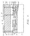
- FIG. 1shows a cross section of the interconnection scheme of the present invention.
- FIG. 2shows a cross section of the present invention in a more complex circuit configuration.
- FIG. 3 ashows the top view of a combination power and X-signal plane using the present invention.
- FIG. 3 bshows the top view of a combination power and Y-signal plane using the present invention.
- FIG. 4shows the top view of solder bump arrangement using the present invention and is an expanded view of a portion of FIG. 5 .
- FIG. 6shows a basic integrated circuit (IC) interconnect scheme of the invention.
- FIG. 7shows an extension of the basic IC interconnect scheme by adding power, ground and signal distribution capabilities.
- FIG. 9shows detail regarding BGA device fan out using the invention.
- FIG. 10shows detail regarding BGA device pad relocation using the invention.
- FIG. 11shows detail regarding the usage of common power, ground and signal pads for BGA devices using the invention.
- the present inventionteaches an Integrated Circuit structure where key re-distribution and interconnection metal layers and dielectric layers are added over a conventional IC. These re-distribution and interconnection layers allow for wider buses and reduce conventional RC delay.
- a silicon substrate 1has transistors and other devices, typically formed of poly silicon, covered by a dielectric layer 2 deposited over the devices and the substrate.
- Layer 3indicates the totality of metal layers 3 ′ and dielectric layers 3 ′′ that are typically created on top of the device layer 2 .
- Points of contact 6such as bonding pads known in the semiconductor art, are in the top surface of layer 3 ′ and are part of layer 3 . These points of contact 6 are points within the IC arrangement that need to be further connected to surrounding circuitry, that is to power lines or to signal lines.
- a passivation layer 4formed of for example silicon nitride, is deposited on top of layer 3 , as is known in the art for protecting underlying layers from moisture, contamination, etc.
- the key steps of the inventionbegin with the deposition of a thick layer 5 of polyimide is deposited.
- a pattern 7is exposed and etched through the polyimide layer 5 and the passivation layer 4 where the pattern 7 is the same as the pattern of the contact points 6 . This opens the contact points 6 up to the surface 8 of the polyimide layer 5 .
- Electrical contact with the contact points 6can now be established by filling the openings 7 with a conductor.
- the tops 9 of this metal conductorcan now be used for connection of the IC to its environment, and for further integration into the surrounding electrical circuitry.
- Pads 10 , 11 and 12are formed on top of the top 9 of the metal conductors 7 ; these pads can be of any design in width and thickness to accommodate specific circuit design requirements.
- a larger size padcan, for instance, be used as a flip chip pad.
- a somewhat smaller in size padcan be used for power distribution or as a ground or signal bus.
- the following connectionscan, for instance, be made to the pads shown in FIG.
- pad 10can serve as a flip chip pad
- pad 11can serve as a flip chip pad or can be connected to electrical power or to electrical ground or to an electrical signal bus
- pad 12can also serve as a flip chip pad.
- Pad size and the standard rules and restrictions of electrical circuit designdetermine the electrical connections to which a given pad lends itself.
- the contact points 6relate to the size and the number of the contact points 6 , FIG. 1 . Because these contact points 6 are located on top of a thin dielectric (layer 3 ′′, FIG. 1 ) the pad size cannot be too large since a large pad size brings with it a large capacitance. In addition, a large pad size will interfere with the routing capability of that layer of metal. It is therefore preferred to keep the size of the pad 6 small.
- the size of pad 6is however also directly related with the aspect ratio of via 7 . An aspect ratio of about 5 is acceptable for the consideration of via etching and via filling. Based on these considerations, the size of the contact pad 6 can be in the order of 0.3 ⁇ m to 5.0 ⁇ m, the exact size being dependent on the thickness of layers 4 and 5 .
- the contact points 6can comprise any appropriate contact material, such as but not limited to tungsten, copper (electroplated or electroless), aluminum, polysilicon, or the like.
- the most frequently used passivation layer in the present state of the artis plasma enhanced CVD (PECVD) oxide and nitride.
- PECVDplasma enhanced CVD
- a layer of between about 0.15 and 2.0 ⁇ m PECVD oxideis deposited first followed by a layer of between about 0.5 and 2.0 ⁇ m, and preferably approximately 0.7 ⁇ m nitride.
- Passivation layer 4is very important because it protects the device wafer from moisture and foreign ion contamination.
- the positioning of this layer between the sub-micron process (of the integrated circuit) and the tens-micron process (of the interconnecting metallization structure)is of critical importance since it allows for a cheaper process that possibly has less stringent clean room requirements for the process of creating the interconnecting metallization structure.
- Layer 5is a thick polymer dielectric layer (for example polyimide) that has a thickness in excess of 2 ⁇ m (after curing).
- the range of polyimide thicknesscan vary from 2 ⁇ m to 30 ⁇ m dependent on electrical design requirements.
- the Hitachi-Dupont polyimide HD 2732 or 2734can, for example, be used.
- the polyimidecan be spin-on coated and cured. After spin-on coating, the polyimide will be cured at between approximately 250 and 450 degrees C., preferably at 400 degrees C., for between approximately 0.5 and 1.5 hours, preferably for 1 hour, in a vacuum or nitrogen ambient.
- the polyimide filmcan be multiple coated and cured.
- BCBpolymer benzocyclobutene
- opening 7has previously been discussed.
- the dimension of the opening together with the dielectric thicknessdetermines the aspect ratio of the opening.
- the aspect ratiochallenges the via etch process and the metal filling capability. This leads to a diameter for opening 7 in the range of approximately 0.5 ⁇ m to 3.0 ⁇ m while the height for opening 7 can be in the range of approximately 3 ⁇ m to 20 ⁇ m.
- the aspect ratio of opening 7is designed such that filling of the via with metal can be accomplished.
- the viacan be filled with CVD metal such as CVD tungsten or CVD copper, with electroless nickel, with a damascene metal filling process, with electroplating copper, with sputtering aluminum, etc.
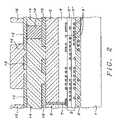
- FIG. 2shows how the present invention as indicated in FIG. 1 can be further extended to include multiple layers of polyimide and, in so doing, can be adapted to a larger variety of applications.
- the lower level build up of this cross sectionis identical to the build up shown in FIG. 1 with a silicon wafer 1 , the poly silicon layer 2 , the metal and dielectric combined layer 3 , the passivation layer 4 , the polyimide layer 5 and the pads 10 deposited on top of layer 5 .
- the function of the structure that has been described in FIG. 1can be further extended by depositing another layer of polyimide 14 on top of the previously deposited layer 5 and overlaying the pads 10 . Selective etching and metal deposition can further create contact points 12 .
- These contact points 12can be connected with pads 10 as shown by connector 13 . Depositing pads 12 on top of layer 14 can thus further extend this process. These pads 12 can be further customized to a particular application, the indicated extension of multiple layers of polyimides greatly enhances the flexibility and usefulness of the present invention. Additional alternating layers of polyimide and metal lines and/or power or ground planes may be added above layers 12 and 16 , as needed. Dielectric layers 14 and 16 can be formed as described above with reference to FIG. 1 for the dielectric layer 5 .
- FIGS. 3 a and 3 bshow a top view of one possible use of the present invention.
- Interconnecting a number of pads 32 that have been created as describedcreates signal lines 30 .
- Additional contact pointssuch as point 34 can allow signal lines to pass vertically between layers.
- the various contact pointscan, for instance, be created within the surface of a power plane or ground plane 36 .
- the layers within the interconnecting metallization structure of the present inventioncan contain signal interconnections in the X-direction, signal interconnections in the Y-direction, signal interconnections between X and or Y directions, interconnections to and/or within power and/or ground buses.
- the present inventionfurther teaches the interconnection of signal lines, power and ground buses between the connected IC's and the top of the metallization system of the present invention.
- FIG. 3 ashows signal lines formed in the X-direction.
- FIG. 3 bshows signal lines formed in the Y-direction.
- FIG. 5shows the top surface of a plane that contains a design pattern of a combination of power or ground pads 52 and signal pads 54 .
- FIG. 5shows the pad openings in the top dielectric layer.
- the number of power or ground pads 52 shown in FIG. 5can be reduced if there are power and/or ground planes within the chip 53 . From this it is clear that the package number of I/O's can be reduced within the scope of the present invention which leads to a reduction of the package cost by eliminating common signal/power/ground connections within the package. For instance, a 470 I/O count on a BGA chip can, within the scope of the present invention, be reduced to a 256 I/O count using the present invention. This results in considerable savings for the overall package.
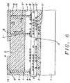
- FIG. 6shows a basic design advantage of the invention. This advantage allows for the sub-micron or fine-lines, that run in the immediate vicinity of the metal layers 3 ′ and the contact points 6 , to be extended in an upward direction 20 through metal interconnect 7 ′. This extension continues in the direction 22 in the horizontal plane of the metal interconnect 26 and comes back down in the downward direction 24 though metal interconnect 7 ′′.
- the functions and constructs of the passivation layer 4 and the insulating layer 5remain as previously highlighted under FIG. 1 .
- This basic design advantage of the inventionis to “elevate” or “fan-out” the fine-line interconnects and to remove these interconnects from the micron and sub-micron level to a metal interconnect level that has considerably larger dimensions and is therefore characterized by smaller resistance and capacitance and is easier and more cost effective to manufacture.
- This aspect of the inventiondoes not include any aspect of conducting line re-distribution and therefore has an inherent quality of simplicity. It therefore further adds to the importance of the invention in that it makes micron and sub-micron wiring accessible at a wide-metal level.
- the interconnections 7 ′ and 7 ′′interconnect the fine-level metal by going up through the passivation and polymer or polyimide dielectric layers, traverses over a distance on the wide-metal level and continues by descending from the wide-metal level back down to the fine-metal level by again traversing down through the passivation and polymer or polyimide dielectric layers.
- the extensions that are in this manner accomplishedneed not to be limited to extending fine-metal interconnect points 6 of any particular type, such as signal or power or ground, with wide metal line 26 .
- the laws of physics and electronicswill impose limitations, if any, as to what type of interconnect can by established in this manner where limiting factors will be the conventional limiting factors of resistance, propagation delay, RC constants and others.
- the upper metallization structure over the passivation layer 4may comprise any appropriate contact material, such as but not limited to tungsten, chromium, copper (electroplated or electroless), aluminum, polysilicon, or the like.
- the upper metallization structure over the passivation layer 4 and over the contact points 6can be formed using a process comprising an electroplating process, a sputtering process, an electroless-plating process, or a damascene process. Where the invention is of importance is that the invention provides much broader latitude in being able to apply these laws and, in so doing, provides a considerably extended scope of the application and use of Integrated Circuits and the adaptation of these circuits to a wide-metal environment.
- the upper metallization structuremay have multiple metal layers and multiple dielectric layers as depicted in FIG. 2 .
- the upper metallization structuremay comprise multiple metal traces and a metal plane, such as a power plane or ground plane, enclosing the metal traces as shown in FIGS. 3 a and 3 b.
- FIG. 7shows how the basic interconnect aspect of the invention can further be extended to now not only elevate the fine-metal to the plane of the wide-metal but to also add power, ground and signal distribution interconnects of power, ground and signal planes at the wide-metal level.
- the wide-metal interconnect 26 of FIG. 6is now extended to further include an interconnection with the via 21 .
- some padsmay not be positioned in a location from which easy fan-out can be accomplished to a location that is required for the next step of circuit assembly.
- the BGA substraterequires additional layers in the package construction in order to accomplish the required fan-out.
- the inventionteaches an approach that makes additional layers in the assembling of an IC feasible while not unduly increasing the cost of creating such a multi-layer interface.
- Ball formation 28 on the surface of interconnect 23indicates how the invention replaces part of the conventional BGA interconnect function, the solder bump provides for flip chip assembly.
- This interconnect 28now connects the BGA device with surrounding circuitry at the wide-metal level as opposed to previous interconnects of the BGA device at the fine-metal level.
- the wide-metal interconnect of the BGAhas obvious advantages of cost of manufacturing and improved BGA device performance.
- FIG. 8further shows a cross section wherein the previous linear construction of the metal interconnection running through the passivation layer and the insulation layer is now conical in form.
- the sub-micron metal layer 60is covered with a passivation layer 62 , a layer 64 of polyimide or polymer is deposited over the passivation layer 62 .
- the wide metal level 66is formed on the surface of layer 64 .
- the via 70is shown as having sloping sides, these sloping sides can be achieved by controlling the photolithography process that is used to created the via 70 .
- the etching of the polyimide or polymercan for instance be done under an angle of about 75 degrees with the following curing being done under an angle of 45 degrees.
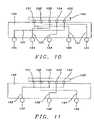
- FIGS. 9 through 11show further detail to demonstrate the concepts of BGA chip ball fan-out, pad relocation and the creation of common ground, power and signal pads.
- the concept of pad relocation, fan-out, pad addition or pad reductioncan be realized by forming the wide and thick metal interconnection scheme over the passivation layer described in this invention, to replace the function of BGA substrate 130 .
- FIG. 9shows a cross section 100 of a BGA chip, five balls 101 through 105 are also shown.
- ball 101can be repositioned to location 111 , ball 102 to location 112 , etc. for the remaining solder bumps 103 through 105 .
- the separation of contact points 111 through 115is considerably larger than the separation of the original solder bumps 101 through 105 .
- the BGA substrate 106is the subject of the invention, this substrate allows for spreading the distance between the contact points or balls of the BGA device to a considerable degree.
- FIG. 10shows the concept of pad relocation.
- BGA pad 120connects to any of the contact balls 101 through 105 .
- the BGA padscan be arranged in a different and arbitrary sequence that is required for further circuit design or packaging. For instance contact point 101 , which is on the far left side of the BGA device 100 , is re-routed to location 122 which is on the second far right of the BGA substrate 130 .
- the re-arrangements of the other BGA solder bumpscan readily be learned from following the wiring 131 within the substrate 131 and by tracing from solder bump to one of the contact points 122 through 125 of the BGA substrate.
- BGA device solder bump 104is connected to interconnect point 140 of the BGA substrate by means of the wire arrangement 136
- BGA device solder bump 102is connected to interconnect point 142 of the BGA substrate by means of the wire arrangement 134 .
- the number of pins required to interconnect the BGA device 100is in this manner reduced from five to three. It is clear that for more BGA device solder bumps, as is the case for an actual BGA device, the numeric effect of the indicated wiring arrangement is considerably more beneficial.
- Fan-out capabilitycan be provided by the invention, using the metal conductors within the openings through the insulating layer and through the passivation layer that connect electrical contact pads of the top metallization structure with contact points of the interconnecting metallization structure.
- Each of the electrical contact points of the interconnecting metallization structureis connected directly and sequentially with at least one electrical contact point of the top metallization structure.
- the distance between electrical contact points of the top metallization structureis larger than the distance between electrical contact points of the interconnecting metallization structure by a measurable amount.
- the number of electrical contact pads of the upper metallization structurecan exceed the number of contact points of the interconnecting metallization structure by a considerable amount. This provides an addition effect.
- Pad relocationmay also be accomplished by the method of the invention. Electrical contact points of the top metallization structure are connected with the contact points of the interconnecting metallization structure, directly but not necessarily sequentially, thereby creating a pad relocation effect. In this method, the distance between electrical contact points of the top metallization structure is larger than the distance between the electrical contact points of the interconnecting metallization structure by a measurable amount. The positions of the electrical contact points of the top metallization structure over the passivation layer from a top view are different from that of the contact points of the interconnecting metallization structure exposed by the openings in the passivation layer.
- a reduction effectmay also be accomplished by the method of the invention, wherein common nodes are connected together. Electrical contact points on a top surface of the top metallization structure are connected with contact points of the interconnecting metallization structure exposed by the openings in the passivation layer, where fewer contact points are used in the top metallization structure, since functionally equivalent contact points in the interconnecting metallization structure are connected together. That is, the number of contact points for a particular electrical function among the electrical contact points of the top metallization structure is smaller than the number of electrical contact points of the interconnecting metallization structure exposed by the passivation layer by a measurable amount.
- IC's of reduced sizecan be packaged and inter-connected with other circuit or system components without limiting the performance of the IC's.
Landscapes
- Engineering & Computer Science (AREA)
- Power Engineering (AREA)
- Physics & Mathematics (AREA)
- Computer Hardware Design (AREA)
- Microelectronics & Electronic Packaging (AREA)
- Condensed Matter Physics & Semiconductors (AREA)
- General Physics & Mathematics (AREA)
- Manufacturing & Machinery (AREA)
- Geometry (AREA)
- Internal Circuitry In Semiconductor Integrated Circuit Devices (AREA)
- Semiconductor Integrated Circuits (AREA)
Abstract
Description
- they produce surfaces in which the step heights of underlying features are reduced, and step slopes are gentle and smooth.
- they are available to fill small openings without producing the voids that occur when low-temperature CVD oxide films are deposited.
- the cured polyimide films can tolerate temperatures of up to 500 degrees C. without degradation of their dielectric film characteristics.
- polyimide films have dielectric breakdowns, which are only slightly lower than that of SiO2.
- the dielectric constant of polyimides is smaller than that of silicon nitride and of SiO2.
- the process used to deposit and pattern polyimide films is relatively simple.
Claims (24)
Priority Applications (2)
| Application Number | Priority Date | Filing Date | Title |
|---|---|---|---|
| US11/839,558US7442969B2 (en) | 1998-12-21 | 2007-08-16 | Top layers of metal for high performance IC's |
| US12/203,154US7863654B2 (en) | 1998-12-21 | 2008-09-03 | Top layers of metal for high performance IC's |
Applications Claiming Priority (7)
| Application Number | Priority Date | Filing Date | Title |
|---|---|---|---|
| US21679198A | 1998-12-21 | 1998-12-21 | |
| US09/251,183US6383916B1 (en) | 1998-12-21 | 1999-02-17 | Top layers of metal for high performance IC's |
| US09/972,639US6657310B2 (en) | 1998-12-21 | 2001-10-09 | Top layers of metal for high performance IC's |
| US10/389,543US6965165B2 (en) | 1998-12-21 | 2003-03-14 | Top layers of metal for high performance IC's |
| US11/121,477US7294870B2 (en) | 1998-12-21 | 2005-05-04 | Top layers of metal for high performance IC's |
| US11/230,102US7368376B2 (en) | 1998-12-21 | 2005-09-19 | Top layers of metal for high performance IC's |
| US11/839,558US7442969B2 (en) | 1998-12-21 | 2007-08-16 | Top layers of metal for high performance IC's |
Related Parent Applications (1)
| Application Number | Title | Priority Date | Filing Date |
|---|---|---|---|
| US11/230,102ContinuationUS7368376B2 (en) | 1998-12-21 | 2005-09-19 | Top layers of metal for high performance IC's |
Related Child Applications (1)
| Application Number | Title | Priority Date | Filing Date |
|---|---|---|---|
| US12/203,154ContinuationUS7863654B2 (en) | 1998-12-21 | 2008-09-03 | Top layers of metal for high performance IC's |
Publications (2)
| Publication Number | Publication Date |
|---|---|
| US20070273038A1 US20070273038A1 (en) | 2007-11-29 |
| US7442969B2true US7442969B2 (en) | 2008-10-28 |
Family
ID=39197209
Family Applications (67)
| Application Number | Title | Priority Date | Filing Date |
|---|---|---|---|
| US10/389,543Expired - LifetimeUS6965165B2 (en) | 1998-12-21 | 2003-03-14 | Top layers of metal for high performance IC's |
| US11/121,477Expired - Fee RelatedUS7294870B2 (en) | 1998-12-21 | 2005-05-04 | Top layers of metal for high performance IC's |
| US11/130,917Expired - Fee RelatedUS7329954B2 (en) | 1998-12-21 | 2005-05-17 | Top layers of metal for high performance IC's |
| US11/131,481Expired - Fee RelatedUS7372155B2 (en) | 1998-12-21 | 2005-05-18 | Top layers of metal for high performance IC's |
| US11/145,468Expired - Fee RelatedUS7384864B2 (en) | 1998-12-21 | 2005-06-03 | Top layers of metal for high performance IC's |
| US11/149,092Expired - Fee RelatedUS7422976B2 (en) | 1998-12-21 | 2005-06-09 | Top layers of metal for high performance IC's |
| US11/230,102Expired - Fee RelatedUS7368376B2 (en) | 1998-12-21 | 2005-09-19 | Top layers of metal for high performance IC's |
| US11/230,101Expired - Fee RelatedUS7372085B2 (en) | 1998-12-21 | 2005-09-19 | Top layers of metal for high performance IC's |
| US11/230,004Expired - Fee RelatedUS7294871B2 (en) | 1998-12-21 | 2005-09-19 | Top layers of metal for high performance IC's |
| US11/829,106AbandonedUS20070262459A1 (en) | 1998-12-21 | 2007-07-27 | Top layers of metal for high performance IC's |
| US11/829,107AbandonedUS20070262460A1 (en) | 1998-12-21 | 2007-07-27 | Top layers of metal for high performance IC's |
| US11/829,109Expired - Fee RelatedUS7999384B2 (en) | 1998-12-21 | 2007-07-27 | Top layers of metal for high performance IC's |
| US11/829,108Expired - Fee RelatedUS7358610B2 (en) | 1998-12-21 | 2007-07-27 | Top layers of metal for high performance IC's |
| US11/829,110Expired - Fee RelatedUS8531038B2 (en) | 1998-12-21 | 2007-07-27 | Top layers of metal for high performance IC's |
| US11/829,105Expired - Fee RelatedUS7385291B2 (en) | 1998-12-21 | 2007-07-27 | Top layers of metal for high performance IC's |
| US11/833,225AbandonedUS20070267714A1 (en) | 1998-12-21 | 2007-08-02 | Top layers of metal for high performance IC's |
| US11/839,558Expired - Fee RelatedUS7442969B2 (en) | 1998-12-21 | 2007-08-16 | Top layers of metal for high performance IC's |
| US11/839,561AbandonedUS20070273041A1 (en) | 1998-12-21 | 2007-08-16 | Top layers of metal for high performance IC's |
| US11/839,559Expired - Fee RelatedUS7397135B2 (en) | 1998-12-21 | 2007-08-16 | Top layers of metal for high performance IC's |
| US11/839,560AbandonedUS20070273040A1 (en) | 1998-12-21 | 2007-08-16 | Top layers of metal for high performance IC's |
| US11/839,550AbandonedUS20070273032A1 (en) | 1998-12-21 | 2007-08-16 | Top layers of metal for high performance IC's |
| US11/839,554Expired - Fee RelatedUS7884479B2 (en) | 1998-12-21 | 2007-08-16 | Top layers of metal for high performance IC's |
| US11/839,556AbandonedUS20070273036A1 (en) | 1998-12-21 | 2007-08-16 | Top layers of metal for high performance IC's |
| US11/839,557AbandonedUS20070273037A1 (en) | 1998-12-21 | 2007-08-16 | Top layers of metal for high performance IC's |
| US11/839,552AbandonedUS20070273034A1 (en) | 1998-12-21 | 2007-08-16 | Top layers of metal for high performance IC's |
| US11/839,551AbandonedUS20070273033A1 (en) | 1998-12-21 | 2007-08-16 | Top layers of metal for high performance IC's |
| US11/840,237AbandonedUS20070281463A1 (en) | 1998-12-21 | 2007-08-17 | Top layers of metal for high performance IC's |
| US11/840,231AbandonedUS20070278684A1 (en) | 1998-12-21 | 2007-08-17 | Top layers of metal for high performance IC's |
| US11/840,238AbandonedUS20070278686A1 (en) | 1998-12-21 | 2007-08-17 | Top layers of metal for high performance IC's |
| US11/840,232AbandonedUS20070278685A1 (en) | 1998-12-21 | 2007-08-17 | Top layers of metal for high performance IC's |
| US11/840,230AbandonedUS20070278688A1 (en) | 1998-12-21 | 2007-08-17 | Top layers of metal for high performance IC's |
| US11/840,241AbandonedUS20070281458A1 (en) | 1998-12-21 | 2007-08-17 | Top layers of metal for high performance IC's |
| US11/840,243AbandonedUS20070278691A1 (en) | 1998-12-21 | 2007-08-17 | Top layers of metal for high performance IC's |
| US11/840,233AbandonedUS20070278689A1 (en) | 1998-12-21 | 2007-08-17 | Top layers of metal for high performance IC's |
| US11/840,242Expired - Fee RelatedUS7425764B2 (en) | 1998-12-21 | 2007-08-17 | Top layers of metal for high performance IC's |
| US11/893,659AbandonedUS20070288880A1 (en) | 1998-12-21 | 2007-08-17 | Top layers of metal for high performance IC's |
| US11/840,234AbandonedUS20070278690A1 (en) | 1998-12-21 | 2007-08-17 | Top layers of metal for high performance IC's |
| US11/840,235AbandonedUS20070281467A1 (en) | 1998-12-21 | 2007-08-17 | Top layers of metal for high performance IC's |
| US11/840,236AbandonedUS20070281468A1 (en) | 1998-12-21 | 2007-08-17 | Top layers of metal for high performance IC's |
| US11/840,239Expired - Fee RelatedUS7465975B2 (en) | 1998-12-21 | 2007-08-17 | Top layers of metal for high performance IC's |
| US11/842,159AbandonedUS20070284753A1 (en) | 1998-12-21 | 2007-08-21 | Top layers of metal for high performance IC's |
| US11/842,160Expired - Fee RelatedUS7482693B2 (en) | 1998-12-21 | 2007-08-21 | Top layers of metal for high performance IC's |
| US11/842,158AbandonedUS20070284751A1 (en) | 1998-12-21 | 2007-08-21 | Top layers of metal for high performance IC's |
| US11/842,161AbandonedUS20070284752A1 (en) | 1998-12-21 | 2007-08-21 | Top layers of metal for high performance IC's |
| US11/842,153Expired - Fee RelatedUS8471384B2 (en) | 1998-12-21 | 2007-08-21 | Top layers of metal for high performance IC's |
| US11/845,759AbandonedUS20070290355A1 (en) | 1998-12-21 | 2007-08-27 | Top layers of metal for high performance IC's |
| US11/845,764AbandonedUS20070290356A1 (en) | 1998-12-21 | 2007-08-27 | Top layers of metal for high performance IC's |
| US11/845,773AbandonedUS20070293036A1 (en) | 1998-12-21 | 2007-08-27 | Top layers of metal for high performance IC's |
| US11/845,116Expired - Fee RelatedUS7388292B2 (en) | 1998-12-21 | 2007-08-27 | Top layers of metal for high performance IC's |
| US11/845,110AbandonedUS20070290349A1 (en) | 1998-12-21 | 2007-08-27 | Top layers of metal for high performance IC's |
| US11/845,115Expired - Fee RelatedUS7385292B2 (en) | 1998-12-21 | 2007-08-27 | Top layers of metal for high performance IC's |
| US11/845,109AbandonedUS20070290348A1 (en) | 1998-12-21 | 2007-08-27 | Top layers of metal for high performance IC's |
| US11/845,122AbandonedUS20070290354A1 (en) | 1998-12-21 | 2007-08-27 | Top layers of metal for high performance IC's |
| US11/845,775Expired - Fee RelatedUS7396756B2 (en) | 1998-12-21 | 2007-08-27 | Top layers of metal for high performance IC's |
| US11/845,113AbandonedUS20070290351A1 (en) | 1998-12-21 | 2007-08-27 | Top layers of metal for high performance IC's |
| US11/845,771AbandonedUS20070290358A1 (en) | 1998-12-21 | 2007-08-27 | Top layers of metal for high performance IC's |
| US11/845,766Expired - Fee RelatedUS7382058B2 (en) | 1998-12-21 | 2007-08-27 | Top layers of metal for high performance IC's |
| US11/845,111AbandonedUS20070290350A1 (en) | 1998-12-21 | 2007-08-27 | Top layers of metal for high performance IC's |
| US11/845,123Expired - Fee RelatedUS8415800B2 (en) | 1998-12-21 | 2007-08-27 | Top layers of metal for high performance IC's |
| US11/930,191Expired - Fee RelatedUS7456100B2 (en) | 1998-12-21 | 2007-10-31 | Top layers of metal for high performance IC's |
| US11/930,189AbandonedUS20080083988A1 (en) | 1998-12-21 | 2007-10-31 | Top layers of metal for high performance IC's |
| US11/930,185AbandonedUS20080083987A1 (en) | 1998-12-21 | 2007-10-31 | Top layers of metal for high performance IC's |
| US11/930,187AbandonedUS20080048329A1 (en) | 1998-12-21 | 2007-10-31 | Top layers of metal for high performance IC's |
| US12/036,308Expired - Fee RelatedUS8022545B2 (en) | 1998-12-21 | 2008-02-25 | Top layers of metal for high performance IC's |
| US12/036,306AbandonedUS20080142980A1 (en) | 1998-12-21 | 2008-02-25 | Top layers of metal for high performance IC's |
| US12/036,309AbandonedUS20080146020A1 (en) | 1998-12-21 | 2008-02-25 | Top layers of metal for high performance IC's |
| US12/203,154Expired - Fee RelatedUS7863654B2 (en) | 1998-12-21 | 2008-09-03 | Top layers of metal for high performance IC's |
Family Applications Before (16)
| Application Number | Title | Priority Date | Filing Date |
|---|---|---|---|
| US10/389,543Expired - LifetimeUS6965165B2 (en) | 1998-12-21 | 2003-03-14 | Top layers of metal for high performance IC's |
| US11/121,477Expired - Fee RelatedUS7294870B2 (en) | 1998-12-21 | 2005-05-04 | Top layers of metal for high performance IC's |
| US11/130,917Expired - Fee RelatedUS7329954B2 (en) | 1998-12-21 | 2005-05-17 | Top layers of metal for high performance IC's |
| US11/131,481Expired - Fee RelatedUS7372155B2 (en) | 1998-12-21 | 2005-05-18 | Top layers of metal for high performance IC's |
| US11/145,468Expired - Fee RelatedUS7384864B2 (en) | 1998-12-21 | 2005-06-03 | Top layers of metal for high performance IC's |
| US11/149,092Expired - Fee RelatedUS7422976B2 (en) | 1998-12-21 | 2005-06-09 | Top layers of metal for high performance IC's |
| US11/230,102Expired - Fee RelatedUS7368376B2 (en) | 1998-12-21 | 2005-09-19 | Top layers of metal for high performance IC's |
| US11/230,101Expired - Fee RelatedUS7372085B2 (en) | 1998-12-21 | 2005-09-19 | Top layers of metal for high performance IC's |
| US11/230,004Expired - Fee RelatedUS7294871B2 (en) | 1998-12-21 | 2005-09-19 | Top layers of metal for high performance IC's |
| US11/829,106AbandonedUS20070262459A1 (en) | 1998-12-21 | 2007-07-27 | Top layers of metal for high performance IC's |
| US11/829,107AbandonedUS20070262460A1 (en) | 1998-12-21 | 2007-07-27 | Top layers of metal for high performance IC's |
| US11/829,109Expired - Fee RelatedUS7999384B2 (en) | 1998-12-21 | 2007-07-27 | Top layers of metal for high performance IC's |
| US11/829,108Expired - Fee RelatedUS7358610B2 (en) | 1998-12-21 | 2007-07-27 | Top layers of metal for high performance IC's |
| US11/829,110Expired - Fee RelatedUS8531038B2 (en) | 1998-12-21 | 2007-07-27 | Top layers of metal for high performance IC's |
| US11/829,105Expired - Fee RelatedUS7385291B2 (en) | 1998-12-21 | 2007-07-27 | Top layers of metal for high performance IC's |
| US11/833,225AbandonedUS20070267714A1 (en) | 1998-12-21 | 2007-08-02 | Top layers of metal for high performance IC's |
Family Applications After (50)
| Application Number | Title | Priority Date | Filing Date |
|---|---|---|---|
| US11/839,561AbandonedUS20070273041A1 (en) | 1998-12-21 | 2007-08-16 | Top layers of metal for high performance IC's |
| US11/839,559Expired - Fee RelatedUS7397135B2 (en) | 1998-12-21 | 2007-08-16 | Top layers of metal for high performance IC's |
| US11/839,560AbandonedUS20070273040A1 (en) | 1998-12-21 | 2007-08-16 | Top layers of metal for high performance IC's |
| US11/839,550AbandonedUS20070273032A1 (en) | 1998-12-21 | 2007-08-16 | Top layers of metal for high performance IC's |
| US11/839,554Expired - Fee RelatedUS7884479B2 (en) | 1998-12-21 | 2007-08-16 | Top layers of metal for high performance IC's |
| US11/839,556AbandonedUS20070273036A1 (en) | 1998-12-21 | 2007-08-16 | Top layers of metal for high performance IC's |
| US11/839,557AbandonedUS20070273037A1 (en) | 1998-12-21 | 2007-08-16 | Top layers of metal for high performance IC's |
| US11/839,552AbandonedUS20070273034A1 (en) | 1998-12-21 | 2007-08-16 | Top layers of metal for high performance IC's |
| US11/839,551AbandonedUS20070273033A1 (en) | 1998-12-21 | 2007-08-16 | Top layers of metal for high performance IC's |
| US11/840,237AbandonedUS20070281463A1 (en) | 1998-12-21 | 2007-08-17 | Top layers of metal for high performance IC's |
| US11/840,231AbandonedUS20070278684A1 (en) | 1998-12-21 | 2007-08-17 | Top layers of metal for high performance IC's |
| US11/840,238AbandonedUS20070278686A1 (en) | 1998-12-21 | 2007-08-17 | Top layers of metal for high performance IC's |
| US11/840,232AbandonedUS20070278685A1 (en) | 1998-12-21 | 2007-08-17 | Top layers of metal for high performance IC's |
| US11/840,230AbandonedUS20070278688A1 (en) | 1998-12-21 | 2007-08-17 | Top layers of metal for high performance IC's |
| US11/840,241AbandonedUS20070281458A1 (en) | 1998-12-21 | 2007-08-17 | Top layers of metal for high performance IC's |
| US11/840,243AbandonedUS20070278691A1 (en) | 1998-12-21 | 2007-08-17 | Top layers of metal for high performance IC's |
| US11/840,233AbandonedUS20070278689A1 (en) | 1998-12-21 | 2007-08-17 | Top layers of metal for high performance IC's |
| US11/840,242Expired - Fee RelatedUS7425764B2 (en) | 1998-12-21 | 2007-08-17 | Top layers of metal for high performance IC's |
| US11/893,659AbandonedUS20070288880A1 (en) | 1998-12-21 | 2007-08-17 | Top layers of metal for high performance IC's |
| US11/840,234AbandonedUS20070278690A1 (en) | 1998-12-21 | 2007-08-17 | Top layers of metal for high performance IC's |
| US11/840,235AbandonedUS20070281467A1 (en) | 1998-12-21 | 2007-08-17 | Top layers of metal for high performance IC's |
| US11/840,236AbandonedUS20070281468A1 (en) | 1998-12-21 | 2007-08-17 | Top layers of metal for high performance IC's |
| US11/840,239Expired - Fee RelatedUS7465975B2 (en) | 1998-12-21 | 2007-08-17 | Top layers of metal for high performance IC's |
| US11/842,159AbandonedUS20070284753A1 (en) | 1998-12-21 | 2007-08-21 | Top layers of metal for high performance IC's |
| US11/842,160Expired - Fee RelatedUS7482693B2 (en) | 1998-12-21 | 2007-08-21 | Top layers of metal for high performance IC's |
| US11/842,158AbandonedUS20070284751A1 (en) | 1998-12-21 | 2007-08-21 | Top layers of metal for high performance IC's |
| US11/842,161AbandonedUS20070284752A1 (en) | 1998-12-21 | 2007-08-21 | Top layers of metal for high performance IC's |
| US11/842,153Expired - Fee RelatedUS8471384B2 (en) | 1998-12-21 | 2007-08-21 | Top layers of metal for high performance IC's |
| US11/845,759AbandonedUS20070290355A1 (en) | 1998-12-21 | 2007-08-27 | Top layers of metal for high performance IC's |
| US11/845,764AbandonedUS20070290356A1 (en) | 1998-12-21 | 2007-08-27 | Top layers of metal for high performance IC's |
| US11/845,773AbandonedUS20070293036A1 (en) | 1998-12-21 | 2007-08-27 | Top layers of metal for high performance IC's |
| US11/845,116Expired - Fee RelatedUS7388292B2 (en) | 1998-12-21 | 2007-08-27 | Top layers of metal for high performance IC's |
| US11/845,110AbandonedUS20070290349A1 (en) | 1998-12-21 | 2007-08-27 | Top layers of metal for high performance IC's |
| US11/845,115Expired - Fee RelatedUS7385292B2 (en) | 1998-12-21 | 2007-08-27 | Top layers of metal for high performance IC's |
| US11/845,109AbandonedUS20070290348A1 (en) | 1998-12-21 | 2007-08-27 | Top layers of metal for high performance IC's |
| US11/845,122AbandonedUS20070290354A1 (en) | 1998-12-21 | 2007-08-27 | Top layers of metal for high performance IC's |
| US11/845,775Expired - Fee RelatedUS7396756B2 (en) | 1998-12-21 | 2007-08-27 | Top layers of metal for high performance IC's |
| US11/845,113AbandonedUS20070290351A1 (en) | 1998-12-21 | 2007-08-27 | Top layers of metal for high performance IC's |
| US11/845,771AbandonedUS20070290358A1 (en) | 1998-12-21 | 2007-08-27 | Top layers of metal for high performance IC's |
| US11/845,766Expired - Fee RelatedUS7382058B2 (en) | 1998-12-21 | 2007-08-27 | Top layers of metal for high performance IC's |
| US11/845,111AbandonedUS20070290350A1 (en) | 1998-12-21 | 2007-08-27 | Top layers of metal for high performance IC's |
| US11/845,123Expired - Fee RelatedUS8415800B2 (en) | 1998-12-21 | 2007-08-27 | Top layers of metal for high performance IC's |
| US11/930,191Expired - Fee RelatedUS7456100B2 (en) | 1998-12-21 | 2007-10-31 | Top layers of metal for high performance IC's |
| US11/930,189AbandonedUS20080083988A1 (en) | 1998-12-21 | 2007-10-31 | Top layers of metal for high performance IC's |
| US11/930,185AbandonedUS20080083987A1 (en) | 1998-12-21 | 2007-10-31 | Top layers of metal for high performance IC's |
| US11/930,187AbandonedUS20080048329A1 (en) | 1998-12-21 | 2007-10-31 | Top layers of metal for high performance IC's |
| US12/036,308Expired - Fee RelatedUS8022545B2 (en) | 1998-12-21 | 2008-02-25 | Top layers of metal for high performance IC's |
| US12/036,306AbandonedUS20080142980A1 (en) | 1998-12-21 | 2008-02-25 | Top layers of metal for high performance IC's |
| US12/036,309AbandonedUS20080146020A1 (en) | 1998-12-21 | 2008-02-25 | Top layers of metal for high performance IC's |
| US12/203,154Expired - Fee RelatedUS7863654B2 (en) | 1998-12-21 | 2008-09-03 | Top layers of metal for high performance IC's |
Country Status (1)
| Country | Link |
|---|---|
| US (67) | US6965165B2 (en) |
Cited By (2)
| Publication number | Priority date | Publication date | Assignee | Title |
|---|---|---|---|---|
| US20070273035A1 (en)* | 1998-12-21 | 2007-11-29 | Mou-Shiung Lin | Top layers of metal for high performance IC's |
| US7960269B2 (en) | 2005-07-22 | 2011-06-14 | Megica Corporation | Method for forming a double embossing structure |
Families Citing this family (291)
| Publication number | Priority date | Publication date | Assignee | Title |
|---|---|---|---|---|
| US8018058B2 (en)* | 2004-06-21 | 2011-09-13 | Besang Inc. | Semiconductor memory device |
| US8058142B2 (en)* | 1996-11-04 | 2011-11-15 | Besang Inc. | Bonded semiconductor structure and method of making the same |
| US6869870B2 (en) | 1998-12-21 | 2005-03-22 | Megic Corporation | High performance system-on-chip discrete components using post passivation process |
| US7932603B2 (en)* | 2001-12-13 | 2011-04-26 | Megica Corporation | Chip structure and process for forming the same |
| TW544882B (en) | 2001-12-31 | 2003-08-01 | Megic Corp | Chip package structure and process thereof |
| TW503496B (en) | 2001-12-31 | 2002-09-21 | Megic Corp | Chip packaging structure and manufacturing process of the same |
| TW584950B (en) | 2001-12-31 | 2004-04-21 | Megic Corp | Chip packaging structure and process thereof |
| US6673698B1 (en)* | 2002-01-19 | 2004-01-06 | Megic Corporation | Thin film semiconductor package utilizing a glass substrate with composite polymer/metal interconnect layers |
| US7096581B2 (en)* | 2002-03-06 | 2006-08-29 | Stmicroelectronics, Inc. | Method for providing a redistribution metal layer in an integrated circuit |
| TWI278962B (en)* | 2002-04-12 | 2007-04-11 | Hitachi Ltd | Semiconductor device |
| US20070197030A1 (en)* | 2002-10-10 | 2007-08-23 | Samsung Electronics Co., Ltd. | Center pad type ic chip with jumpers, method of processing the same and multi chip package |
| JP4357862B2 (en)* | 2003-04-09 | 2009-11-04 | シャープ株式会社 | Semiconductor device |
| US20100190334A1 (en)* | 2003-06-24 | 2010-07-29 | Sang-Yun Lee | Three-dimensional semiconductor structure and method of manufacturing the same |
| US7863748B2 (en)* | 2003-06-24 | 2011-01-04 | Oh Choonsik | Semiconductor circuit and method of fabricating the same |
| US8071438B2 (en) | 2003-06-24 | 2011-12-06 | Besang Inc. | Semiconductor circuit |
| US7005369B2 (en)* | 2003-08-21 | 2006-02-28 | Intersil American Inc. | Active area bonding compatible high current structures |
| US8274160B2 (en) | 2003-08-21 | 2012-09-25 | Intersil Americas Inc. | Active area bonding compatible high current structures |
| JP4397210B2 (en) | 2003-10-20 | 2010-01-13 | ローム株式会社 | Semiconductor device |
| CN1617312A (en) | 2003-11-10 | 2005-05-18 | 松下电器产业株式会社 | Semiconductor device and manufacturing method thereof |
| US8367524B2 (en) | 2005-03-29 | 2013-02-05 | Sang-Yun Lee | Three-dimensional integrated circuit structure |
| US8279912B2 (en)* | 2006-03-13 | 2012-10-02 | Plx Technology, Inc. | Tranceiver non-linearity cancellation |
| DE102006032073B4 (en)* | 2006-07-11 | 2016-07-07 | Intel Deutschland Gmbh | Electrically conductive composite of a component and a carrier plate |
| US8427844B2 (en)* | 2006-08-28 | 2013-04-23 | Avago Technologies Ecbu Ip (Singapore) Pte. Ltd. | Widebody coil isolators |
| US7652378B2 (en)* | 2006-10-17 | 2010-01-26 | Taiwan Semiconductor Manufacturing Company, Ltd. | Aluminum-based interconnection in bond pad layer |
| JPWO2008126468A1 (en)* | 2007-03-30 | 2010-07-22 | 日本電気株式会社 | Semiconductor device and manufacturing method of semiconductor device |
| US7951697B1 (en) | 2007-06-20 | 2011-05-31 | Amkor Technology, Inc. | Embedded die metal etch stop fabrication method and structure |
| US7923645B1 (en) | 2007-06-20 | 2011-04-12 | Amkor Technology, Inc. | Metal etch stop fabrication method and structure |
| US7958626B1 (en)* | 2007-10-25 | 2011-06-14 | Amkor Technology, Inc. | Embedded passive component network substrate fabrication method |
| SG155096A1 (en)* | 2008-03-03 | 2009-09-30 | Micron Technology Inc | Board-on-chip type substrates with conductive traces in multiple planes, semiconductor device packages including such substrates, and associated methods |
| JP2010153543A (en)* | 2008-12-25 | 2010-07-08 | Fujitsu Ltd | Semiconductor device and method of manufacturing the same |
| US7847408B2 (en)* | 2009-01-16 | 2010-12-07 | Oracle America, Inc. | Integrated clock and power distribution |
| US8870018B2 (en)* | 2009-02-27 | 2014-10-28 | Lbp Manufacturing, Inc. | Sleeve for a container |
| US9509313B2 (en) | 2009-04-14 | 2016-11-29 | Monolithic 3D Inc. | 3D semiconductor device |
| US8362800B2 (en) | 2010-10-13 | 2013-01-29 | Monolithic 3D Inc. | 3D semiconductor device including field repairable logics |
| US8384426B2 (en) | 2009-04-14 | 2013-02-26 | Monolithic 3D Inc. | Semiconductor device and structure |
| US8427200B2 (en) | 2009-04-14 | 2013-04-23 | Monolithic 3D Inc. | 3D semiconductor device |
| US8754533B2 (en) | 2009-04-14 | 2014-06-17 | Monolithic 3D Inc. | Monolithic three-dimensional semiconductor device and structure |
| US8378715B2 (en) | 2009-04-14 | 2013-02-19 | Monolithic 3D Inc. | Method to construct systems |
| US8405420B2 (en) | 2009-04-14 | 2013-03-26 | Monolithic 3D Inc. | System comprising a semiconductor device and structure |
| US8373439B2 (en) | 2009-04-14 | 2013-02-12 | Monolithic 3D Inc. | 3D semiconductor device |
| US8058137B1 (en) | 2009-04-14 | 2011-11-15 | Monolithic 3D Inc. | Method for fabrication of a semiconductor device and structure |
| US9711407B2 (en) | 2009-04-14 | 2017-07-18 | Monolithic 3D Inc. | Method of manufacturing a three dimensional integrated circuit by transfer of a mono-crystalline layer |
| US8395191B2 (en) | 2009-10-12 | 2013-03-12 | Monolithic 3D Inc. | Semiconductor device and structure |
| US8362482B2 (en) | 2009-04-14 | 2013-01-29 | Monolithic 3D Inc. | Semiconductor device and structure |
| US9577642B2 (en) | 2009-04-14 | 2017-02-21 | Monolithic 3D Inc. | Method to form a 3D semiconductor device |
| US8669778B1 (en) | 2009-04-14 | 2014-03-11 | Monolithic 3D Inc. | Method for design and manufacturing of a 3D semiconductor device |
| US7986042B2 (en) | 2009-04-14 | 2011-07-26 | Monolithic 3D Inc. | Method for fabrication of a semiconductor device and structure |
| US8278733B2 (en)* | 2009-08-25 | 2012-10-02 | Mediatek Inc. | Bonding pad structure and integrated circuit chip using such bonding pad structure |
| US12027518B1 (en) | 2009-10-12 | 2024-07-02 | Monolithic 3D Inc. | 3D semiconductor devices and structures with metal layers |
| US8581349B1 (en) | 2011-05-02 | 2013-11-12 | Monolithic 3D Inc. | 3D memory semiconductor device and structure |
| US11018133B2 (en) | 2009-10-12 | 2021-05-25 | Monolithic 3D Inc. | 3D integrated circuit |
| US10157909B2 (en) | 2009-10-12 | 2018-12-18 | Monolithic 3D Inc. | 3D semiconductor device and structure |
| US11984445B2 (en) | 2009-10-12 | 2024-05-14 | Monolithic 3D Inc. | 3D semiconductor devices and structures with metal layers |
| US10366970B2 (en) | 2009-10-12 | 2019-07-30 | Monolithic 3D Inc. | 3D semiconductor device and structure |
| US10354995B2 (en) | 2009-10-12 | 2019-07-16 | Monolithic 3D Inc. | Semiconductor memory device and structure |
| US8476145B2 (en) | 2010-10-13 | 2013-07-02 | Monolithic 3D Inc. | Method of fabricating a semiconductor device and structure |
| US8742476B1 (en) | 2012-11-27 | 2014-06-03 | Monolithic 3D Inc. | Semiconductor device and structure |
| US8450804B2 (en) | 2011-03-06 | 2013-05-28 | Monolithic 3D Inc. | Semiconductor device and structure for heat removal |
| US8536023B2 (en) | 2010-11-22 | 2013-09-17 | Monolithic 3D Inc. | Method of manufacturing a semiconductor device and structure |
| US8148728B2 (en) | 2009-10-12 | 2012-04-03 | Monolithic 3D, Inc. | Method for fabrication of a semiconductor device and structure |
| US9099424B1 (en) | 2012-08-10 | 2015-08-04 | Monolithic 3D Inc. | Semiconductor system, device and structure with heat removal |
| US10388863B2 (en) | 2009-10-12 | 2019-08-20 | Monolithic 3D Inc. | 3D memory device and structure |
| US11374118B2 (en) | 2009-10-12 | 2022-06-28 | Monolithic 3D Inc. | Method to form a 3D integrated circuit |
| US10043781B2 (en) | 2009-10-12 | 2018-08-07 | Monolithic 3D Inc. | 3D semiconductor device and structure |
| US10910364B2 (en) | 2009-10-12 | 2021-02-02 | Monolitaic 3D Inc. | 3D semiconductor device |
| US8502394B2 (en)* | 2009-12-31 | 2013-08-06 | Stmicroelectronics Pte Ltd. | Multi-stacked semiconductor dice scale package structure and method of manufacturing same |
| US8436255B2 (en)* | 2009-12-31 | 2013-05-07 | Stmicroelectronics Pte Ltd. | Fan-out wafer level package with polymeric layer for high reliability |
| US20110156240A1 (en)* | 2009-12-31 | 2011-06-30 | Stmicroelectronics Asia Pacific Pte. Ltd. | Reliable large die fan-out wafer level package and method of manufacture |
| US8466997B2 (en)* | 2009-12-31 | 2013-06-18 | Stmicroelectronics Pte Ltd. | Fan-out wafer level package for an optical sensor and method of manufacture thereof |
| US8884422B2 (en)* | 2009-12-31 | 2014-11-11 | Stmicroelectronics Pte Ltd. | Flip-chip fan-out wafer level package for package-on-package applications, and method of manufacture |
| US8492886B2 (en) | 2010-02-16 | 2013-07-23 | Monolithic 3D Inc | 3D integrated circuit with logic |
| US9099526B2 (en) | 2010-02-16 | 2015-08-04 | Monolithic 3D Inc. | Integrated circuit device and structure |
| US8541819B1 (en) | 2010-12-09 | 2013-09-24 | Monolithic 3D Inc. | Semiconductor device and structure |
| US8373230B1 (en) | 2010-10-13 | 2013-02-12 | Monolithic 3D Inc. | Method for fabrication of a semiconductor device and structure |
| US8461035B1 (en) | 2010-09-30 | 2013-06-11 | Monolithic 3D Inc. | Method for fabrication of a semiconductor device and structure |
| US8026521B1 (en) | 2010-10-11 | 2011-09-27 | Monolithic 3D Inc. | Semiconductor device and structure |
| CN101964188B (en)* | 2010-04-09 | 2012-09-05 | 华为技术有限公司 | Voice signal coding and decoding methods, devices and systems |
| KR101134819B1 (en) | 2010-07-02 | 2012-04-13 | 이상윤 | Method for fabricating semiconductor memory |
| US8642416B2 (en) | 2010-07-30 | 2014-02-04 | Monolithic 3D Inc. | Method of forming three dimensional integrated circuit devices using layer transfer technique |
| US8901613B2 (en) | 2011-03-06 | 2014-12-02 | Monolithic 3D Inc. | Semiconductor device and structure for heat removal |
| US10217667B2 (en) | 2011-06-28 | 2019-02-26 | Monolithic 3D Inc. | 3D semiconductor device, fabrication method and system |
| US9219005B2 (en) | 2011-06-28 | 2015-12-22 | Monolithic 3D Inc. | Semiconductor system and device |
| US9953925B2 (en) | 2011-06-28 | 2018-04-24 | Monolithic 3D Inc. | Semiconductor system and device |
| US8343810B2 (en) | 2010-08-16 | 2013-01-01 | Stats Chippac, Ltd. | Semiconductor device and method of forming Fo-WLCSP having conductive layers and conductive vias separated by polymer layers |
| US8163581B1 (en) | 2010-10-13 | 2012-04-24 | Monolith IC 3D | Semiconductor and optoelectronic devices |
| US8273610B2 (en) | 2010-11-18 | 2012-09-25 | Monolithic 3D Inc. | Method of constructing a semiconductor device and structure |
| US11482440B2 (en) | 2010-12-16 | 2022-10-25 | Monolithic 3D Inc. | 3D semiconductor device and structure with a built-in test circuit for repairing faulty circuits |
| US10497713B2 (en) | 2010-11-18 | 2019-12-03 | Monolithic 3D Inc. | 3D semiconductor memory device and structure |
| US12362219B2 (en) | 2010-11-18 | 2025-07-15 | Monolithic 3D Inc. | 3D semiconductor memory device and structure |
| US11227897B2 (en) | 2010-10-11 | 2022-01-18 | Monolithic 3D Inc. | Method for producing a 3D semiconductor memory device and structure |
| US11257867B1 (en) | 2010-10-11 | 2022-02-22 | Monolithic 3D Inc. | 3D semiconductor device and structure with oxide bonds |
| US11469271B2 (en) | 2010-10-11 | 2022-10-11 | Monolithic 3D Inc. | Method to produce 3D semiconductor devices and structures with memory |
| US10896931B1 (en) | 2010-10-11 | 2021-01-19 | Monolithic 3D Inc. | 3D semiconductor device and structure |
| US11024673B1 (en) | 2010-10-11 | 2021-06-01 | Monolithic 3D Inc. | 3D semiconductor device and structure |
| US11600667B1 (en) | 2010-10-11 | 2023-03-07 | Monolithic 3D Inc. | Method to produce 3D semiconductor devices and structures with memory |
| US8114757B1 (en) | 2010-10-11 | 2012-02-14 | Monolithic 3D Inc. | Semiconductor device and structure |
| US11158674B2 (en) | 2010-10-11 | 2021-10-26 | Monolithic 3D Inc. | Method to produce a 3D semiconductor device and structure |
| US11018191B1 (en) | 2010-10-11 | 2021-05-25 | Monolithic 3D Inc. | 3D semiconductor device and structure |
| US10290682B2 (en) | 2010-10-11 | 2019-05-14 | Monolithic 3D Inc. | 3D IC semiconductor device and structure with stacked memory |
| US11315980B1 (en) | 2010-10-11 | 2022-04-26 | Monolithic 3D Inc. | 3D semiconductor device and structure with transistors |
| US11605663B2 (en) | 2010-10-13 | 2023-03-14 | Monolithic 3D Inc. | Multilevel semiconductor device and structure with image sensors and wafer bonding |
| US10833108B2 (en) | 2010-10-13 | 2020-11-10 | Monolithic 3D Inc. | 3D microdisplay device and structure |
| US11869915B2 (en) | 2010-10-13 | 2024-01-09 | Monolithic 3D Inc. | Multilevel semiconductor device and structure with image sensors and wafer bonding |
| US11163112B2 (en) | 2010-10-13 | 2021-11-02 | Monolithic 3D Inc. | Multilevel semiconductor device and structure with electromagnetic modulators |
| US11694922B2 (en) | 2010-10-13 | 2023-07-04 | Monolithic 3D Inc. | Multilevel semiconductor device and structure with oxide bonding |
| US11164898B2 (en) | 2010-10-13 | 2021-11-02 | Monolithic 3D Inc. | Multilevel semiconductor device and structure |
| US11063071B1 (en) | 2010-10-13 | 2021-07-13 | Monolithic 3D Inc. | Multilevel semiconductor device and structure with waveguides |
| US11929372B2 (en) | 2010-10-13 | 2024-03-12 | Monolithic 3D Inc. | Multilevel semiconductor device and structure with image sensors and wafer bonding |
| US11984438B2 (en) | 2010-10-13 | 2024-05-14 | Monolithic 3D Inc. | Multilevel semiconductor device and structure with oxide bonding |
| US11327227B2 (en) | 2010-10-13 | 2022-05-10 | Monolithic 3D Inc. | Multilevel semiconductor device and structure with electromagnetic modulators |
| US12094892B2 (en) | 2010-10-13 | 2024-09-17 | Monolithic 3D Inc. | 3D micro display device and structure |
| US10679977B2 (en) | 2010-10-13 | 2020-06-09 | Monolithic 3D Inc. | 3D microdisplay device and structure |
| US9197804B1 (en) | 2011-10-14 | 2015-11-24 | Monolithic 3D Inc. | Semiconductor and optoelectronic devices |
| US8379458B1 (en) | 2010-10-13 | 2013-02-19 | Monolithic 3D Inc. | Semiconductor device and structure |
| US11855100B2 (en) | 2010-10-13 | 2023-12-26 | Monolithic 3D Inc. | Multilevel semiconductor device and structure with oxide bonding |
| US10943934B2 (en) | 2010-10-13 | 2021-03-09 | Monolithic 3D Inc. | Multilevel semiconductor device and structure |
| US11437368B2 (en) | 2010-10-13 | 2022-09-06 | Monolithic 3D Inc. | Multilevel semiconductor device and structure with oxide bonding |
| US10978501B1 (en) | 2010-10-13 | 2021-04-13 | Monolithic 3D Inc. | Multilevel semiconductor device and structure with waveguides |
| US11133344B2 (en) | 2010-10-13 | 2021-09-28 | Monolithic 3D Inc. | Multilevel semiconductor device and structure with image sensors |
| US11043523B1 (en) | 2010-10-13 | 2021-06-22 | Monolithic 3D Inc. | Multilevel semiconductor device and structure with image sensors |
| US10998374B1 (en) | 2010-10-13 | 2021-05-04 | Monolithic 3D Inc. | Multilevel semiconductor device and structure |
| US12080743B2 (en) | 2010-10-13 | 2024-09-03 | Monolithic 3D Inc. | Multilevel semiconductor device and structure with image sensors and wafer bonding |
| US12360310B2 (en) | 2010-10-13 | 2025-07-15 | Monolithic 3D Inc. | Multilevel semiconductor device and structure with oxide bonding |
| US11855114B2 (en) | 2010-10-13 | 2023-12-26 | Monolithic 3D Inc. | Multilevel semiconductor device and structure with image sensors and wafer bonding |
| US11404466B2 (en) | 2010-10-13 | 2022-08-02 | Monolithic 3D Inc. | Multilevel semiconductor device and structure with image sensors |
| US11443971B2 (en) | 2010-11-18 | 2022-09-13 | Monolithic 3D Inc. | 3D semiconductor device and structure with memory |
| US11211279B2 (en) | 2010-11-18 | 2021-12-28 | Monolithic 3D Inc. | Method for processing a 3D integrated circuit and structure |
| US11735462B2 (en) | 2010-11-18 | 2023-08-22 | Monolithic 3D Inc. | 3D semiconductor device and structure with single-crystal layers |
| US11610802B2 (en) | 2010-11-18 | 2023-03-21 | Monolithic 3D Inc. | Method for producing a 3D semiconductor device and structure with single crystal transistors and metal gate electrodes |
| US11923230B1 (en) | 2010-11-18 | 2024-03-05 | Monolithic 3D Inc. | 3D semiconductor device and structure with bonding |
| US11784082B2 (en) | 2010-11-18 | 2023-10-10 | Monolithic 3D Inc. | 3D semiconductor device and structure with bonding |
| US11508605B2 (en) | 2010-11-18 | 2022-11-22 | Monolithic 3D Inc. | 3D semiconductor memory device and structure |
| US11004719B1 (en) | 2010-11-18 | 2021-05-11 | Monolithic 3D Inc. | Methods for producing a 3D semiconductor memory device and structure |
| US11094576B1 (en) | 2010-11-18 | 2021-08-17 | Monolithic 3D Inc. | Methods for producing a 3D semiconductor memory device and structure |
| US11107721B2 (en) | 2010-11-18 | 2021-08-31 | Monolithic 3D Inc. | 3D semiconductor device and structure with NAND logic |
| US11482439B2 (en) | 2010-11-18 | 2022-10-25 | Monolithic 3D Inc. | Methods for producing a 3D semiconductor memory device comprising charge trap junction-less transistors |
| US12033884B2 (en) | 2010-11-18 | 2024-07-09 | Monolithic 3D Inc. | Methods for producing a 3D semiconductor device and structure with memory cells and multiple metal layers |
| US11521888B2 (en) | 2010-11-18 | 2022-12-06 | Monolithic 3D Inc. | 3D semiconductor device and structure with high-k metal gate transistors |
| US11862503B2 (en) | 2010-11-18 | 2024-01-02 | Monolithic 3D Inc. | Method for producing a 3D semiconductor device and structure with memory cells and multiple metal layers |
| US11355381B2 (en) | 2010-11-18 | 2022-06-07 | Monolithic 3D Inc. | 3D semiconductor memory device and structure |
| US11482438B2 (en) | 2010-11-18 | 2022-10-25 | Monolithic 3D Inc. | Methods for producing a 3D semiconductor memory device and structure |
| US12272586B2 (en) | 2010-11-18 | 2025-04-08 | Monolithic 3D Inc. | 3D semiconductor memory device and structure with memory and metal layers |
| US11901210B2 (en) | 2010-11-18 | 2024-02-13 | Monolithic 3D Inc. | 3D semiconductor device and structure with memory |
| US11569117B2 (en) | 2010-11-18 | 2023-01-31 | Monolithic 3D Inc. | 3D semiconductor device and structure with single-crystal layers |
| US12136562B2 (en) | 2010-11-18 | 2024-11-05 | Monolithic 3D Inc. | 3D semiconductor device and structure with single-crystal layers |
| US12068187B2 (en) | 2010-11-18 | 2024-08-20 | Monolithic 3D Inc. | 3D semiconductor device and structure with bonding and DRAM memory cells |
| US11615977B2 (en) | 2010-11-18 | 2023-03-28 | Monolithic 3D Inc. | 3D semiconductor memory device and structure |
| US12144190B2 (en) | 2010-11-18 | 2024-11-12 | Monolithic 3D Inc. | 3D semiconductor device and structure with bonding and memory cells preliminary class |
| US12100611B2 (en) | 2010-11-18 | 2024-09-24 | Monolithic 3D Inc. | Methods for producing a 3D semiconductor device and structure with memory cells and multiple metal layers |
| US12125737B1 (en) | 2010-11-18 | 2024-10-22 | Monolithic 3D Inc. | 3D semiconductor device and structure with metal layers and memory cells |
| US11018042B1 (en) | 2010-11-18 | 2021-05-25 | Monolithic 3D Inc. | 3D semiconductor memory device and structure |
| US11031275B2 (en) | 2010-11-18 | 2021-06-08 | Monolithic 3D Inc. | 3D semiconductor device and structure with memory |
| US11121021B2 (en) | 2010-11-18 | 2021-09-14 | Monolithic 3D Inc. | 3D semiconductor device and structure |
| US11355380B2 (en) | 2010-11-18 | 2022-06-07 | Monolithic 3D Inc. | Methods for producing 3D semiconductor memory device and structure utilizing alignment marks |
| US11164770B1 (en) | 2010-11-18 | 2021-11-02 | Monolithic 3D Inc. | Method for producing a 3D semiconductor memory device and structure |
| US11804396B2 (en) | 2010-11-18 | 2023-10-31 | Monolithic 3D Inc. | Methods for producing a 3D semiconductor device and structure with memory cells and multiple metal layers |
| US12243765B2 (en) | 2010-11-18 | 2025-03-04 | Monolithic 3D Inc. | 3D semiconductor device and structure with metal layers and memory cells |
| US12154817B1 (en) | 2010-11-18 | 2024-11-26 | Monolithic 3D Inc. | Methods for producing a 3D semiconductor memory device and structure |
| US11495484B2 (en) | 2010-11-18 | 2022-11-08 | Monolithic 3D Inc. | 3D semiconductor devices and structures with at least two single-crystal layers |
| US11854857B1 (en) | 2010-11-18 | 2023-12-26 | Monolithic 3D Inc. | Methods for producing a 3D semiconductor device and structure with memory cells and multiple metal layers |
| US8791501B1 (en) | 2010-12-03 | 2014-07-29 | Amkor Technology, Inc. | Integrated passive device structure and method |
| US8975670B2 (en) | 2011-03-06 | 2015-03-10 | Monolithic 3D Inc. | Semiconductor device and structure for heat removal |
| US10388568B2 (en) | 2011-06-28 | 2019-08-20 | Monolithic 3D Inc. | 3D semiconductor device and system |
| US9013037B2 (en) | 2011-09-14 | 2015-04-21 | Stmicroelectronics Pte Ltd. | Semiconductor package with improved pillar bump process and structure |
| US8687399B2 (en) | 2011-10-02 | 2014-04-01 | Monolithic 3D Inc. | Semiconductor device and structure |
| US9029173B2 (en) | 2011-10-18 | 2015-05-12 | Monolithic 3D Inc. | Method for fabrication of a semiconductor device and structure |
| US8779601B2 (en) | 2011-11-02 | 2014-07-15 | Stmicroelectronics Pte Ltd | Embedded wafer level package for 3D and package-on-package applications, and method of manufacture |
| US8916481B2 (en) | 2011-11-02 | 2014-12-23 | Stmicroelectronics Pte Ltd. | Embedded wafer level package for 3D and package-on-package applications, and method of manufacture |
| US8717136B2 (en) | 2012-01-10 | 2014-05-06 | International Business Machines Corporation | Inductor with laminated yoke |
| US20130221974A1 (en)* | 2012-02-29 | 2013-08-29 | GM Global Technology Operations LLC | Time domain reflectometry system and method |
| US9000557B2 (en) | 2012-03-17 | 2015-04-07 | Zvi Or-Bach | Semiconductor device and structure |
| US8557632B1 (en) | 2012-04-09 | 2013-10-15 | Monolithic 3D Inc. | Method for fabrication of a semiconductor device and structure |
| US11735501B1 (en) | 2012-04-09 | 2023-08-22 | Monolithic 3D Inc. | 3D semiconductor device and structure with metal layers and a connective path |
| US11476181B1 (en) | 2012-04-09 | 2022-10-18 | Monolithic 3D Inc. | 3D semiconductor device and structure with metal layers |
| US11694944B1 (en) | 2012-04-09 | 2023-07-04 | Monolithic 3D Inc. | 3D semiconductor device and structure with metal layers and a connective path |
| US11881443B2 (en) | 2012-04-09 | 2024-01-23 | Monolithic 3D Inc. | 3D semiconductor device and structure with metal layers and a connective path |
| US11164811B2 (en) | 2012-04-09 | 2021-11-02 | Monolithic 3D Inc. | 3D semiconductor device with isolation layers and oxide-to-oxide bonding |
| US11088050B2 (en) | 2012-04-09 | 2021-08-10 | Monolithic 3D Inc. | 3D semiconductor device with isolation layers |
| US11594473B2 (en) | 2012-04-09 | 2023-02-28 | Monolithic 3D Inc. | 3D semiconductor device and structure with metal layers and a connective path |
| US11616004B1 (en) | 2012-04-09 | 2023-03-28 | Monolithic 3D Inc. | 3D semiconductor device and structure with metal layers and a connective path |
| US11410912B2 (en) | 2012-04-09 | 2022-08-09 | Monolithic 3D Inc. | 3D semiconductor device with vias and isolation layers |
| US10600888B2 (en) | 2012-04-09 | 2020-03-24 | Monolithic 3D Inc. | 3D semiconductor device |
| US8779592B2 (en)* | 2012-05-01 | 2014-07-15 | Taiwan Semiconductor Manufacturing Company, Ltd. | Via-free interconnect structure with self-aligned metal line interconnections |
| US9064628B2 (en) | 2012-05-22 | 2015-06-23 | International Business Machines Corporation | Inductor with stacked conductors |
| TWI583195B (en) | 2012-07-06 | 2017-05-11 | 新力股份有限公司 | A solid-state imaging device and a solid-state imaging device, and an electronic device |
| KR101985937B1 (en)* | 2012-07-11 | 2019-06-05 | 삼성전자주식회사 | Semiconductor devices and method of manufacturing the same |
| WO2014026858A1 (en)* | 2012-08-14 | 2014-02-20 | Sony Corporation | Integrated semiconductor device |
| JP6044240B2 (en)* | 2012-10-01 | 2016-12-14 | 株式会社ソシオネクスト | Semiconductor device and semiconductor device design method |
| US8686428B1 (en) | 2012-11-16 | 2014-04-01 | Monolithic 3D Inc. | Semiconductor device and structure |
| US8574929B1 (en) | 2012-11-16 | 2013-11-05 | Monolithic 3D Inc. | Method to form a 3D semiconductor device and structure |
| US11961827B1 (en) | 2012-12-22 | 2024-04-16 | Monolithic 3D Inc. | 3D semiconductor device and structure with metal layers |
| US12051674B2 (en) | 2012-12-22 | 2024-07-30 | Monolithic 3D Inc. | 3D semiconductor device and structure with metal layers |
| US11063024B1 (en) | 2012-12-22 | 2021-07-13 | Monlithic 3D Inc. | Method to form a 3D semiconductor device and structure |
| US8674470B1 (en) | 2012-12-22 | 2014-03-18 | Monolithic 3D Inc. | Semiconductor device and structure |
| US11784169B2 (en) | 2012-12-22 | 2023-10-10 | Monolithic 3D Inc. | 3D semiconductor device and structure with metal layers |
| US11018116B2 (en) | 2012-12-22 | 2021-05-25 | Monolithic 3D Inc. | Method to form a 3D semiconductor device and structure |
| US11450646B1 (en)* | 2012-12-22 | 2022-09-20 | Monolithic 3D Inc. | 3D semiconductor device and structure with metal layers |
| US11309292B2 (en) | 2012-12-22 | 2022-04-19 | Monolithic 3D Inc. | 3D semiconductor device and structure with metal layers |
| US11217565B2 (en) | 2012-12-22 | 2022-01-04 | Monolithic 3D Inc. | Method to form a 3D semiconductor device and structure |
| US11967583B2 (en) | 2012-12-22 | 2024-04-23 | Monolithic 3D Inc. | 3D semiconductor device and structure with metal layers |
| US11916045B2 (en) | 2012-12-22 | 2024-02-27 | Monolithic 3D Inc. | 3D semiconductor device and structure with metal layers |
| US11177140B2 (en) | 2012-12-29 | 2021-11-16 | Monolithic 3D Inc. | 3D semiconductor device and structure |
| US9871034B1 (en) | 2012-12-29 | 2018-01-16 | Monolithic 3D Inc. | Semiconductor device and structure |
| US10651054B2 (en) | 2012-12-29 | 2020-05-12 | Monolithic 3D Inc. | 3D semiconductor device and structure |
| US11430667B2 (en) | 2012-12-29 | 2022-08-30 | Monolithic 3D Inc. | 3D semiconductor device and structure with bonding |
| US11087995B1 (en) | 2012-12-29 | 2021-08-10 | Monolithic 3D Inc. | 3D semiconductor device and structure |
| US9385058B1 (en) | 2012-12-29 | 2016-07-05 | Monolithic 3D Inc. | Semiconductor device and structure |
| US12249538B2 (en) | 2012-12-29 | 2025-03-11 | Monolithic 3D Inc. | 3D semiconductor device and structure including power distribution grids |
| US10600657B2 (en) | 2012-12-29 | 2020-03-24 | Monolithic 3D Inc | 3D semiconductor device and structure |
| US10892169B2 (en) | 2012-12-29 | 2021-01-12 | Monolithic 3D Inc. | 3D semiconductor device and structure |
| US11430668B2 (en) | 2012-12-29 | 2022-08-30 | Monolithic 3D Inc. | 3D semiconductor device and structure with bonding |
| US11004694B1 (en) | 2012-12-29 | 2021-05-11 | Monolithic 3D Inc. | 3D semiconductor device and structure |
| US10903089B1 (en) | 2012-12-29 | 2021-01-26 | Monolithic 3D Inc. | 3D semiconductor device and structure |
| US10115663B2 (en) | 2012-12-29 | 2018-10-30 | Monolithic 3D Inc. | 3D semiconductor device and structure |
| US9362187B2 (en)* | 2013-01-18 | 2016-06-07 | Infineon Technologies Ag | Chip package having terminal pads of different form factors |
| US9263511B2 (en)* | 2013-02-11 | 2016-02-16 | Taiwan Semiconductor Manufacturing Co., Ltd. | Package with metal-insulator-metal capacitor and method of manufacturing the same |
| US8902663B1 (en) | 2013-03-11 | 2014-12-02 | Monolithic 3D Inc. | Method of maintaining a memory state |
| US10325651B2 (en) | 2013-03-11 | 2019-06-18 | Monolithic 3D Inc. | 3D semiconductor device with stacked memory |
| US11869965B2 (en) | 2013-03-11 | 2024-01-09 | Monolithic 3D Inc. | 3D semiconductor device and structure with metal layers and memory cells |
| US11935949B1 (en) | 2013-03-11 | 2024-03-19 | Monolithic 3D Inc. | 3D semiconductor device and structure with metal layers and memory cells |
| US12094965B2 (en) | 2013-03-11 | 2024-09-17 | Monolithic 3D Inc. | 3D semiconductor device and structure with metal layers and memory cells |
| US8994404B1 (en) | 2013-03-12 | 2015-03-31 | Monolithic 3D Inc. | Semiconductor device and structure |
| US12100646B2 (en) | 2013-03-12 | 2024-09-24 | Monolithic 3D Inc. | 3D semiconductor device and structure with metal layers |
| US10840239B2 (en) | 2014-08-26 | 2020-11-17 | Monolithic 3D Inc. | 3D semiconductor device and structure |
| US11923374B2 (en) | 2013-03-12 | 2024-03-05 | Monolithic 3D Inc. | 3D semiconductor device and structure with metal layers |
| US11088130B2 (en) | 2014-01-28 | 2021-08-10 | Monolithic 3D Inc. | 3D semiconductor device and structure |
| US11398569B2 (en) | 2013-03-12 | 2022-07-26 | Monolithic 3D Inc. | 3D semiconductor device and structure |
| US9082870B2 (en)* | 2013-03-13 | 2015-07-14 | Taiwan Semiconductor Manufacturing Company, Ltd. | Methods and apparatus of packaging semiconductor devices |
| US10224279B2 (en) | 2013-03-15 | 2019-03-05 | Monolithic 3D Inc. | Semiconductor device and structure |
| US9117749B1 (en) | 2013-03-15 | 2015-08-25 | Monolithic 3D Inc. | Semiconductor device and structure |
| US9021414B1 (en) | 2013-04-15 | 2015-04-28 | Monolithic 3D Inc. | Automation for monolithic 3D devices |
| US11574109B1 (en) | 2013-04-15 | 2023-02-07 | Monolithic 3D Inc | Automation methods for 3D integrated circuits and devices |
| US11720736B2 (en) | 2013-04-15 | 2023-08-08 | Monolithic 3D Inc. | Automation methods for 3D integrated circuits and devices |
| US11487928B2 (en) | 2013-04-15 | 2022-11-01 | Monolithic 3D Inc. | Automation for monolithic 3D devices |
| US11030371B2 (en) | 2013-04-15 | 2021-06-08 | Monolithic 3D Inc. | Automation for monolithic 3D devices |
| US11341309B1 (en) | 2013-04-15 | 2022-05-24 | Monolithic 3D Inc. | Automation for monolithic 3D devices |
| US11270055B1 (en) | 2013-04-15 | 2022-03-08 | Monolithic 3D Inc. | Automation for monolithic 3D devices |
| US9208938B2 (en)* | 2013-10-02 | 2015-12-08 | Globalfoundries Inc. | Inductor structure having embedded airgap |
| US9570342B1 (en)* | 2014-01-17 | 2017-02-14 | Altera Corporation | Via structure and method for its fabrication |
| US10297586B2 (en) | 2015-03-09 | 2019-05-21 | Monolithic 3D Inc. | Methods for processing a 3D semiconductor device |
| US11107808B1 (en) | 2014-01-28 | 2021-08-31 | Monolithic 3D Inc. | 3D semiconductor device and structure |
| US11031394B1 (en) | 2014-01-28 | 2021-06-08 | Monolithic 3D Inc. | 3D semiconductor device and structure |
| US12094829B2 (en) | 2014-01-28 | 2024-09-17 | Monolithic 3D Inc. | 3D semiconductor device and structure |
| WO2015146738A1 (en)* | 2014-03-24 | 2015-10-01 | 技術研究組合光電子融合基盤技術研究所 | Pad-array structure on substrate for mounting ic chip on substrate, and optical module having said pad-array structure |
| US9356009B2 (en) | 2014-05-27 | 2016-05-31 | Micron Technology, Inc. | Interconnect structure with redundant electrical connectors and associated systems and methods |
| US9379079B1 (en)* | 2014-12-29 | 2016-06-28 | Mediatek Inc. | Flip chip scheme and method of forming flip chip scheme |
| DE102016102982A1 (en) | 2015-03-03 | 2016-09-08 | Inglass S.P.A. | Process for the preparation of a component |
| US11011507B1 (en) | 2015-04-19 | 2021-05-18 | Monolithic 3D Inc. | 3D semiconductor device and structure |
| US10825779B2 (en) | 2015-04-19 | 2020-11-03 | Monolithic 3D Inc. | 3D semiconductor device and structure |
| US11056468B1 (en) | 2015-04-19 | 2021-07-06 | Monolithic 3D Inc. | 3D semiconductor device and structure |
| US10381328B2 (en) | 2015-04-19 | 2019-08-13 | Monolithic 3D Inc. | Semiconductor device and structure |
| US11956952B2 (en) | 2015-08-23 | 2024-04-09 | Monolithic 3D Inc. | Semiconductor memory device and structure |
| US11978731B2 (en) | 2015-09-21 | 2024-05-07 | Monolithic 3D Inc. | Method to produce a multi-level semiconductor memory device and structure |
| US12100658B2 (en) | 2015-09-21 | 2024-09-24 | Monolithic 3D Inc. | Method to produce a 3D multilayer semiconductor device and structure |
| US12178055B2 (en) | 2015-09-21 | 2024-12-24 | Monolithic 3D Inc. | 3D semiconductor memory devices and structures |
| CN108401468A (en) | 2015-09-21 | 2018-08-14 | 莫诺利特斯3D有限公司 | 3D semiconductor devices and structures |
| US11937422B2 (en) | 2015-11-07 | 2024-03-19 | Monolithic 3D Inc. | Semiconductor memory device and structure |
| US11114427B2 (en) | 2015-11-07 | 2021-09-07 | Monolithic 3D Inc. | 3D semiconductor processor and memory device and structure |
| US12250830B2 (en) | 2015-09-21 | 2025-03-11 | Monolithic 3D Inc. | 3D semiconductor memory devices and structures |
| US10522225B1 (en) | 2015-10-02 | 2019-12-31 | Monolithic 3D Inc. | Semiconductor device with non-volatile memory |
| US12219769B2 (en) | 2015-10-24 | 2025-02-04 | Monolithic 3D Inc. | 3D semiconductor device and structure with logic and memory |
| US10847540B2 (en) | 2015-10-24 | 2020-11-24 | Monolithic 3D Inc. | 3D semiconductor memory device and structure |
| US11991884B1 (en) | 2015-10-24 | 2024-05-21 | Monolithic 3D Inc. | 3D semiconductor device and structure with logic and memory |
| US12035531B2 (en) | 2015-10-24 | 2024-07-09 | Monolithic 3D Inc. | 3D semiconductor device and structure with logic and memory |
| US10418369B2 (en) | 2015-10-24 | 2019-09-17 | Monolithic 3D Inc. | Multi-level semiconductor memory device and structure |
| US11296115B1 (en) | 2015-10-24 | 2022-04-05 | Monolithic 3D Inc. | 3D semiconductor device and structure |
| US12016181B2 (en) | 2015-10-24 | 2024-06-18 | Monolithic 3D Inc. | 3D semiconductor device and structure with logic and memory |
| US11114464B2 (en) | 2015-10-24 | 2021-09-07 | Monolithic 3D Inc. | 3D semiconductor device and structure |
| US12120880B1 (en) | 2015-10-24 | 2024-10-15 | Monolithic 3D Inc. | 3D semiconductor device and structure with logic and memory |
| US11711928B2 (en) | 2016-10-10 | 2023-07-25 | Monolithic 3D Inc. | 3D memory devices and structures with control circuits |
| US11251149B2 (en) | 2016-10-10 | 2022-02-15 | Monolithic 3D Inc. | 3D memory device and structure |
| US11869591B2 (en) | 2016-10-10 | 2024-01-09 | Monolithic 3D Inc. | 3D memory devices and structures with control circuits |
| US11930648B1 (en) | 2016-10-10 | 2024-03-12 | Monolithic 3D Inc. | 3D memory devices and structures with metal layers |
| US11329059B1 (en) | 2016-10-10 | 2022-05-10 | Monolithic 3D Inc. | 3D memory devices and structures with thinned single crystal substrates |
| US11812620B2 (en) | 2016-10-10 | 2023-11-07 | Monolithic 3D Inc. | 3D DRAM memory devices and structures with control circuits |
| US12225704B2 (en) | 2016-10-10 | 2025-02-11 | Monolithic 3D Inc. | 3D memory devices and structures with memory arrays and metal layers |
| US9929114B1 (en)* | 2016-11-02 | 2018-03-27 | Vanguard International Semiconductor Corporation | Bonding pad structure having island portions and method for manufacturing the same |
| US12322732B2 (en) | 2017-02-09 | 2025-06-03 | Vuereal Inc. | Circuit and system integration onto a microdevice substrate |
| US11916096B2 (en) | 2017-02-09 | 2024-02-27 | Vuereal Inc. | Circuit and system integration onto a micro-device substrate |
| CN107624004A (en)* | 2017-08-22 | 2018-01-23 | 努比亚技术有限公司 | A kind of applying method of printed circuit board (PCB) and a kind of printed circuit board (PCB) |
| JP6888581B2 (en)* | 2018-04-11 | 2021-06-16 | 株式会社デンソー | Semiconductor devices and their manufacturing methods |
| TWI848019B (en)* | 2018-11-16 | 2024-07-11 | 加拿大商弗瑞爾公司 | Microdevice cartridge structure |
| US20200273824A1 (en)* | 2019-02-22 | 2020-08-27 | Intel Corporation | Transceiver die interconnect interfaces |
| US11158652B1 (en) | 2019-04-08 | 2021-10-26 | Monolithic 3D Inc. | 3D memory semiconductor devices and structures |
| US11296106B2 (en) | 2019-04-08 | 2022-04-05 | Monolithic 3D Inc. | 3D memory semiconductor devices and structures |
| US11763864B2 (en) | 2019-04-08 | 2023-09-19 | Monolithic 3D Inc. | 3D memory semiconductor devices and structures with bit-line pillars |
| US10892016B1 (en) | 2019-04-08 | 2021-01-12 | Monolithic 3D Inc. | 3D memory semiconductor devices and structures |
| US11721657B2 (en) | 2019-06-14 | 2023-08-08 | Stmicroelectronics Pte Ltd | Wafer level chip scale package having varying thicknesses |
| KR20210121336A (en) | 2020-03-26 | 2021-10-08 | 삼성전자주식회사 | Semiconductor package |
| CN112349679B (en)* | 2020-10-26 | 2023-09-19 | Oppo广东移动通信有限公司 | Integrated circuit wiring network, integrated circuits, chips and electronic devices |
| US12414312B2 (en)* | 2021-12-20 | 2025-09-09 | International Business Machines Corporation | Back-end-of-line thin film resistor |
Citations (161)
| Publication number | Priority date | Publication date | Assignee | Title |
|---|---|---|---|---|
| US3823349A (en) | 1970-01-22 | 1974-07-09 | Ibm | Interconnection metallurgy system for semiconductor devices |
| US4152195A (en) | 1976-08-27 | 1979-05-01 | International Business Machines Corporation | Method of improving the adherence of metallic conductive lines on polyimide layers |
| US4188636A (en) | 1977-04-01 | 1980-02-12 | Nippon Electric Co., Ltd. | Semiconductor device having bump terminal electrodes |
| US4242336A (en) | 1978-07-31 | 1980-12-30 | Nippon Gohsei Kagaku Kogyo Kabushiki Kaisha | Antibacterial and antifungal composition |
| US4423547A (en) | 1981-06-01 | 1984-01-03 | International Business Machines Corporation | Method for forming dense multilevel interconnection metallurgy for semiconductor devices |
| US4618878A (en) | 1983-06-18 | 1986-10-21 | Kabushiki Kaisha Toshiba | Semiconductor device having a multilayer wiring structure using a polyimide resin |
| US4723197A (en) | 1985-12-16 | 1988-02-02 | National Semiconductor Corporation | Bonding pad interconnection structure |
| US4830974A (en) | 1988-01-11 | 1989-05-16 | Atmel Corporation | EPROM fabrication process |
| JPH01135043A (en) | 1987-11-20 | 1989-05-26 | Toshiba Corp | How to form multilayer wiring |
| JPH01183836A (en) | 1988-01-19 | 1989-07-21 | Sanyo Electric Co Ltd | Manufacture of semiconductor device |
| JPH01184848A (en) | 1988-01-14 | 1989-07-24 | Agency Of Ind Science & Technol | Manufacture of multilayer interconnection |
| JPH01184849A (en) | 1988-01-14 | 1989-07-24 | Agency Of Ind Science & Technol | Manufacture of multilayer interconnection |
| US4881144A (en) | 1987-01-19 | 1989-11-14 | Hitachi, Ltd. | Thin film magnetic head |
| US4978419A (en) | 1986-10-09 | 1990-12-18 | International Business Machines Corporation | Process for defining vias through silicon nitride and polyamide |
| US4980034A (en) | 1989-04-04 | 1990-12-25 | Massachusetts Institute Of Technology | High-density, multi-level interconnects, flex circuits, and tape for TAB |
| US5016461A (en) | 1989-09-01 | 1991-05-21 | Hydro-Craft, Inc. | Method and apparatus for stamping weld adapters |
| US5055907A (en) | 1989-01-25 | 1991-10-08 | Mosaic, Inc. | Extended integration semiconductor structure with wiring layers |
| US5083187A (en) | 1990-05-16 | 1992-01-21 | Texas Instruments Incorporated | Integrated circuit device having bumped power supply buses over active surface areas and method of manufacture thereof |
| US5106461A (en) | 1989-04-04 | 1992-04-21 | Massachusetts Institute Of Technology | High-density, multi-level interconnects, flex circuits, and tape for tab |
| US5130457A (en) | 1986-03-22 | 1992-07-14 | Bayer Aktiengesellschaft | Process for the preparation of n,n-disubstituted mono- and oligourethanes |
| JPH04316351A (en) | 1991-04-16 | 1992-11-06 | Fujitsu Ltd | Manufacture of semiconductor device |
| US5194928A (en) | 1991-01-14 | 1993-03-16 | International Business Machines Corporation | Passivation of metal in metal/polyimide structure |
| US5212403A (en) | 1990-09-10 | 1993-05-18 | Hitachi, Ltd. | Integrated circuit device having an ic chip mounted on the wiring substrate and having suitable mutual connections between internal circuits |
| US5262353A (en) | 1992-02-03 | 1993-11-16 | Motorola, Inc. | Process for forming a structure which electrically shields conductors |
| US5338696A (en) | 1990-04-02 | 1994-08-16 | National Semiconductor Corporation | Method of fabricating BiCMOS device |
| US5360524A (en) | 1993-04-13 | 1994-11-01 | Rudi Hendel | Method for planarization of submicron vias and the manufacture of semiconductor integrated circuits |
| US5384488A (en) | 1992-06-15 | 1995-01-24 | Texas Instruments Incorporated | Configuration and method for positioning semiconductor device bond pads using additional process layers |
| US5436412A (en) | 1992-10-30 | 1995-07-25 | International Business Machines Corporation | Interconnect structure having improved metallization |
| US5468984A (en) | 1994-11-02 | 1995-11-21 | Texas Instruments Incorporated | ESD protection structure using LDMOS diodes with thick copper interconnect |
| US5489303A (en) | 1991-01-25 | 1996-02-06 | Terumo Kabushiki Kaisha | Biocompatible material for medical apparatus comprising hydrophobically bound oil-soluble vitamin |
| US5501006A (en) | 1993-09-22 | 1996-03-26 | Motorola, Inc. | Method for connection of signals to an integrated circuit |
| US5514006A (en) | 1993-02-09 | 1996-05-07 | Leviton Manufacturing Co., Inc. | Turn knob lampholder |
| US5559055A (en) | 1994-12-21 | 1996-09-24 | Advanced Micro Devices, Inc. | Method of decreased interlayer dielectric constant in a multilayer interconnect structure to increase device speed performance |
| US5563086A (en) | 1993-09-13 | 1996-10-08 | International Business Machines Corporation | Integrated memory cube, structure and fabrication |
| US5635767A (en) | 1995-06-02 | 1997-06-03 | Motorola, Inc. | Semiconductor device having built-in high frequency bypass capacitor |
| US5659201A (en) | 1995-06-05 | 1997-08-19 | Advanced Micro Devices, Inc. | High conductivity interconnection line |
| US5665639A (en) | 1994-02-23 | 1997-09-09 | Cypress Semiconductor Corp. | Process for manufacturing a semiconductor device bump electrode using a rapid thermal anneal |
| US5686764A (en) | 1996-03-20 | 1997-11-11 | Lsi Logic Corporation | Flip chip package with reduced number of package layers |
| US5686560A (en) | 1995-06-06 | 1997-11-11 | Hitachi Chemical Co., Ltd. | Polyquinazolines and methods for their preparation |
| US5719448A (en) | 1989-03-07 | 1998-02-17 | Seiko Epson Corporation | Bonding pad structures for semiconductor integrated circuits |
| US5726499A (en) | 1995-07-22 | 1998-03-10 | Ricoh Company, Ltd. | Semiconductor device having a minute contact hole |
| US5739560A (en) | 1994-09-22 | 1998-04-14 | Nippon Telegraph And Telephone Corporation | High frequency masterslice monolithic integrated circuit |
| US5742075A (en) | 1994-10-07 | 1998-04-21 | Iowa State University Research Foundation, Inc. | Amorphous silicon on insulator VLSI circuit structures |
| US5760429A (en) | 1993-06-01 | 1998-06-02 | Matsushita Electric Industrial Co., Ltd. | Multi-layer wiring structure having varying-sized cutouts |
| US5763954A (en) | 1995-08-10 | 1998-06-09 | Mitsubishi Denki Kabushiki Kaisha | Semiconductor device having multilayered metal interconnection structure and manufacturing method thereof |
| US5767010A (en) | 1995-03-20 | 1998-06-16 | Mcnc | Solder bump fabrication methods and structure including a titanium barrier layer |
| US5767546A (en) | 1994-12-30 | 1998-06-16 | Siliconix Incorporated | Laternal power mosfet having metal strap layer to reduce distributed resistance |
| US5773888A (en) | 1994-11-12 | 1998-06-30 | Kabushiki Kaisha Toshiba | Semiconductor device having a bump electrode connected to an inner lead |
| US5783483A (en) | 1993-02-24 | 1998-07-21 | Intel Corporation | Method of fabricating a barrier against metal diffusion |
| US5789303A (en) | 1994-11-28 | 1998-08-04 | Northern Telecom Limited | Method of adding on chip capacitors to an integrated circuit |
| US5818110A (en) | 1996-11-22 | 1998-10-06 | International Business Machines Corporation | Integrated circuit chip wiring structure with crossover capability and method of manufacturing the same |
| US5827776A (en) | 1996-07-18 | 1998-10-27 | Advanced Micro Devices, Inc. | Method of making an integrated circuit which uses an etch stop for producing staggered interconnect lines |
| US5827778A (en) | 1995-11-28 | 1998-10-27 | Nec Corporation | Method of manufacturing a semiconductor device using a silicon fluoride oxide film |
| US5834844A (en) | 1995-03-24 | 1998-11-10 | Shinko Electric Industries Co., Ltd. | Semiconductor device having an element with circuit pattern thereon |
| US5861675A (en) | 1996-12-26 | 1999-01-19 | Kabushiki Kaisha Toshiba | Semiconductor device having WNF film and method of manufacturing such a device |
| US5861328A (en) | 1996-10-07 | 1999-01-19 | Motorola, Inc. | Method of fabricating GMR devices |
| US5874779A (en) | 1994-09-01 | 1999-02-23 | Kabushiki Kaisha Toshiba | Semiconductor device with improved adhesion between titanium-based metal wiring layer and insulation film |
| US5894170A (en) | 1996-08-29 | 1999-04-13 | Nec Corporation | Wiring layer in semiconductor device |
| US5900668A (en) | 1995-11-30 | 1999-05-04 | Advanced Micro Devices, Inc. | Low capacitance interconnection |
| US5910020A (en) | 1995-12-18 | 1999-06-08 | Nec Corporation | Method for fabricating a semiconductor device having a refractory metal pillar for electrical connection |
| US5924005A (en) | 1997-02-18 | 1999-07-13 | Motorola, Inc. | Process for forming a semiconductor device |
| US5934844A (en) | 1995-10-06 | 1999-08-10 | Sandvik Aktiebolag | Cutting insert |
| US5939790A (en) | 1996-04-09 | 1999-08-17 | Altera Corporation | Integrated circuit pad structures |
| US5944537A (en) | 1997-12-15 | 1999-08-31 | Xerox Corporation | Photolithographically patterned spring contact and apparatus and methods for electrically contacting devices |
| US5953626A (en) | 1996-06-05 | 1999-09-14 | Advanced Micro Devices, Inc. | Dissolvable dielectric method |
| US5959424A (en) | 1997-04-11 | 1999-09-28 | Fraunhofer-Gesellschaft Zur Foerderung Der Angewandten Forschung E.V. | Drive device for moving a robot or vehicle on flat, inclined or curved surfaces, particularly of a glass construction and robot with drive device |
| US5963840A (en) | 1996-11-13 | 1999-10-05 | Applied Materials, Inc. | Methods for depositing premetal dielectric layer at sub-atmospheric and high temperature conditions |
| US5965903A (en) | 1995-10-30 | 1999-10-12 | Lucent Technologies Inc. | Device and method of manufacture for an integrated circuit having a BIST circuit and bond pads incorporated therein |
| US5969424A (en) | 1997-03-19 | 1999-10-19 | Fujitsu Limited | Semiconductor device with pad structure |
| US5986764A (en) | 1997-05-12 | 1999-11-16 | Olympus Optical Co., Ltd. | Distance measurement device |
| US5989991A (en) | 1995-03-24 | 1999-11-23 | Integrated Device Technology, Inc. | Methods for fabricating a bonding pad having improved adhesion to an underlying structure |
| US6001673A (en) | 1999-02-11 | 1999-12-14 | Ericsson Inc. | Methods for packaging integrated circuit devices including cavities adjacent active regions |
| US6001538A (en) | 1998-04-06 | 1999-12-14 | Taiwan Semiconductor Manufacturing Company Ltd. | Damage free passivation layer etching process |
| US6016000A (en) | 1998-04-22 | 2000-01-18 | Cvc, Inc. | Ultra high-speed chip semiconductor integrated circuit interconnect structure and fabrication method using free-space dielectrics |
| US6020640A (en) | 1996-12-19 | 2000-02-01 | Texas Instruments Incorporated | Thick plated interconnect and associated auxillary interconnect |
| US6025639A (en) | 1997-03-24 | 2000-02-15 | Siemens Aktiengesellschaft | Crack stops |
| US6025275A (en) | 1996-12-19 | 2000-02-15 | Texas Instruments Incorporated | Method of forming improved thick plated copper interconnect and associated auxiliary metal interconnect |
| US6031257A (en) | 1997-06-13 | 2000-02-29 | Hitachi, Ltd. | Semiconductor integrated circuit device |
| US6033939A (en) | 1998-04-21 | 2000-03-07 | International Business Machines Corporation | Method for providing electrically fusible links in copper interconnection |
| US6046503A (en) | 1997-09-26 | 2000-04-04 | Siemens Aktiengesellschaft | Metalization system having an enhanced thermal conductivity |
| US6100548A (en) | 1997-04-10 | 2000-08-08 | Hughes Electronics Corporation | Modulation-doped field-effect transistors and fabrication processes |
| US6103552A (en) | 1998-08-10 | 2000-08-15 | Lin; Mou-Shiung | Wafer scale packaging scheme |
| US6107674A (en) | 1993-05-05 | 2000-08-22 | Ixys Corporation | Isolated multi-chip devices |
| US6124912A (en) | 1997-06-09 | 2000-09-26 | National Semiconductor Corporation | Reflectance enhancing thin film stack in which pairs of dielectric layers are on a reflector and liquid crystal is on the dielectric layers |
| US6124198A (en) | 1998-04-22 | 2000-09-26 | Cvc, Inc. | Ultra high-speed chip interconnect using free-space dielectrics |
| US6130457A (en) | 1996-04-09 | 2000-10-10 | Samsung Electronics Co., Ltd. | Semiconductor-on-insulator devices having insulating layers therein with self-aligned openings |
| US6130481A (en) | 1991-05-02 | 2000-10-10 | Mitsubishi Denki Kabushiki Kaisha | Semiconductor integrated circuit interconnection structures and method of making the interconnection structures |
| US6133582A (en) | 1998-05-14 | 2000-10-17 | Lightspeed Semiconductor Corporation | Methods and apparatuses for binning partially completed integrated circuits based upon test results |
| US6137155A (en) | 1997-12-31 | 2000-10-24 | Intel Corporation | Planar guard ring |
| US6144100A (en) | 1997-06-05 | 2000-11-07 | Texas Instruments Incorporated | Integrated circuit with bonding layer over active circuitry |
| US6150725A (en) | 1997-02-27 | 2000-11-21 | Sanyo Electric Co., Ltd. | Semiconductor devices with means to reduce contamination |
| US6150726A (en) | 1996-09-06 | 2000-11-21 | International Business Machines Corp. | Component carrier with raised bonding sites |
| US6160297A (en) | 1997-02-10 | 2000-12-12 | Kabushiki Kaisha Toshiba | Semiconductor memory device having a first source line arranged between a memory cell string and bit lines in the direction crossing the bit lines and a second source line arranged in parallel to the bit lines |
| US6169019B1 (en) | 1997-05-14 | 2001-01-02 | Kabushiki Kaisha Toshiba | Semiconductor apparatus and manufacturing method therefor |
| US6175156B1 (en) | 1997-11-21 | 2001-01-16 | Mitsubishi Denki Kabushiki Kaisha | Semiconductor device with improved interconnection |
| US6174393B1 (en) | 1997-03-26 | 2001-01-16 | Kmk Lizence Ltd. | Process for the production of a multi-chamber packaging tube |
| US6184143B1 (en) | 1997-09-08 | 2001-02-06 | Hitachi, Ltd. | Semiconductor integrated circuit device and fabrication process thereof |
| US6184138B1 (en) | 1999-09-07 | 2001-02-06 | Chartered Semiconductor Manufacturing Ltd. | Method to create a controllable and reproducible dual copper damascene structure |
| US6187680B1 (en) | 1998-10-07 | 2001-02-13 | International Business Machines Corporation | Method/structure for creating aluminum wirebound pad on copper BEOL |
| US6207486B1 (en) | 1997-09-12 | 2001-03-27 | Kabushiki Kaisha Toshiba | Semiconductor device and a method of manufacturing the same |
| US6218223B1 (en) | 1990-05-31 | 2001-04-17 | Canon Kabushiki Kaisha | Process for producing electrode for semiconductor element and semiconductor device having the electrode |
| US6218318B1 (en) | 1997-02-05 | 2001-04-17 | Fujitsu Limited | Semiconductor device having a porous insulation film |
| US6229221B1 (en) | 1998-12-04 | 2001-05-08 | U.S. Philips Corporation | Integrated circuit device |
| US6261944B1 (en) | 1998-11-24 | 2001-07-17 | Vantis Corporation | Method for forming a semiconductor device having high reliability passivation overlying a multi-level interconnect |
| US6272736B1 (en) | 1998-11-13 | 2001-08-14 | United Microelectronics Corp. | Method for forming a thin-film resistor |
| US6278174B1 (en) | 1994-04-28 | 2001-08-21 | Texas Instruments Incorporated | Integrated circuit insulator and structure using low dielectric insulator material including HSQ and fluorinated oxide |
| US6288442B1 (en) | 1998-09-10 | 2001-09-11 | Micron Technology, Inc. | Integrated circuit with oxidation-resistant polymeric layer |
| US6294451B1 (en) | 1995-11-10 | 2001-09-25 | Nippon Steel Corporation | Semiconductor device and method for manufacturing the same |
| US6300234B1 (en) | 2000-06-26 | 2001-10-09 | Motorola, Inc. | Process for forming an electrical device |
| US6303423B1 (en) | 1998-12-21 | 2001-10-16 | Megic Corporation | Method for forming high performance system-on-chip using post passivation process |
| US6303977B1 (en) | 1998-12-03 | 2001-10-16 | Texas Instruments Incorporated | Fully hermetic semiconductor chip, including sealed edge sides |
| US20010035452A1 (en) | 2000-03-24 | 2001-11-01 | Test Howard R. | Wire bonding process for copper-metallized integrated circuits |
| US6324048B1 (en) | 1998-03-04 | 2001-11-27 | Avx Corporation | Ultra-small capacitor array |
| US6326673B1 (en) | 1998-08-07 | 2001-12-04 | Windbond Electronics Corp. | Method and structure of manufacturing a high-Q inductor with an air trench |
| US6335104B1 (en) | 2000-02-22 | 2002-01-01 | International Business Machines Corporation | Method for preparing a conductive pad for electrical connection and conductive pad formed |
| US6346471B1 (en) | 1998-05-26 | 2002-02-12 | Nec Corporation | Multilayer wiring structure and semiconductor device having the same, and manufacturing method therefor |
| US20020017730A1 (en) | 2000-08-11 | 2002-02-14 | Integrated Electronics & Packaging | Semiconductor device |
| US6348733B1 (en) | 1999-07-08 | 2002-02-19 | Industrial Technology Research Institute | Dual damascene process and structure with dielectric barrier layer |
| US20020024142A1 (en) | 2000-08-24 | 2002-02-28 | Mitsuru Sekiguchi | Semiconductor device and manufacturing method of the same |
| US6359328B1 (en) | 1998-12-31 | 2002-03-19 | Intel Corporation | Methods for making interconnects and diffusion barriers in integrated circuits |
| US6370768B1 (en) | 1997-07-28 | 2002-04-16 | Hitachi, Ltd. | Circuit board, a method for manufacturing same, and a method of electroless plating |
| US6376374B1 (en) | 1998-05-12 | 2002-04-23 | Semitool, Inc. | Process and manufacturing tool architecture for use in the manufacturing of one or more protected metallization structures on a workpiece |
| US6383916B1 (en) | 1998-12-21 | 2002-05-07 | M. S. Lin | Top layers of metal for high performance IC's |
| US6392300B1 (en) | 1999-06-28 | 2002-05-21 | Kabushiki Kaisha Toshiba | Semiconductor device having an alignment mark formed on the uppermost layer of a multilayer wire |
| US6417575B2 (en) | 2000-06-07 | 2002-07-09 | Mitsubishi Denki Kabushiki Kaisha | Semiconductor device and fabrication process therefor |
| US6436814B1 (en) | 2000-11-21 | 2002-08-20 | International Business Machines Corporation | Interconnection structure and method for fabricating same |
| US6441487B2 (en) | 1997-10-20 | 2002-08-27 | Flip Chip Technologies, L.L.C. | Chip scale package using large ductile solder balls |
| US6455880B1 (en) | 1998-11-06 | 2002-09-24 | Kabushiki Kaisha Toshiba | Microwave semiconductor device having coplanar waveguide and micro-strip line |
| US6459135B1 (en) | 1999-03-23 | 2002-10-01 | Memscap S.A. | Monolithic integrated circuit incorporating an inductive component and process for fabricating such an integrated circuit |
| US6472745B1 (en) | 1999-01-18 | 2002-10-29 | Shinko Electric Industries Co., Ltd. | Semiconductor device |
| US20020158334A1 (en) | 2001-04-30 | 2002-10-31 | Intel Corporation | Microelectronic device having signal distribution functionality on an interfacial layer thereof |
| US6495442B1 (en) | 2000-10-18 | 2002-12-17 | Magic Corporation | Post passivation interconnection schemes on top of the IC chips |
| US6518092B2 (en) | 2000-07-13 | 2003-02-11 | Oki Electric Industry Co., Ltd. | Semiconductor device and method for manufacturing |
| US6538326B2 (en) | 2000-10-16 | 2003-03-25 | Sharp Kabushiki Kaisha | Semiconductor device and manufacturing method thereof |
| US6544880B1 (en) | 1999-06-14 | 2003-04-08 | Micron Technology, Inc. | Method of improving copper interconnects of semiconductor devices for bonding |
| US6555459B1 (en) | 1999-01-25 | 2003-04-29 | Sanyo Electric Co., Ltd. | Method of manufacturing a semiconductor device |
| US6583043B2 (en) | 2001-07-27 | 2003-06-24 | Motorola, Inc. | Dielectric between metal structures and method therefor |
| US6593649B1 (en) | 2001-05-17 | 2003-07-15 | Megic Corporation | Methods of IC rerouting option for multiple package system applications |
| US6605524B1 (en) | 2001-09-10 | 2003-08-12 | Taiwan Semiconductor Manufacturing Company | Bumping process to increase bump height and to create a more robust bump structure |
| US6605549B2 (en) | 2001-09-29 | 2003-08-12 | Intel Corporation | Method for improving nucleation and adhesion of CVD and ALD films deposited onto low-dielectric-constant dielectrics |
| US6614099B2 (en) | 1998-08-04 | 2003-09-02 | Micron Technology, Inc. | Copper metallurgy in integrated circuits |
| US6614091B1 (en) | 2002-03-13 | 2003-09-02 | Motorola, Inc. | Semiconductor device having a wire bond pad and method therefor |
| US6620728B2 (en) | 1998-12-21 | 2003-09-16 | Megic Corporation | Top layers of metal for high performance IC's |
| US6673704B2 (en) | 1996-12-24 | 2004-01-06 | Kabushiki Kaisha Toshiba | Semiconductor device and method of manufacturing the same |
| US6707159B1 (en) | 1999-02-18 | 2004-03-16 | Rohm Co., Ltd. | Semiconductor chip and production process therefor |
| US6709973B1 (en) | 1998-12-18 | 2004-03-23 | Rohm Co., Ltd | Method of fabricating semiconductor device |
| US6710460B2 (en) | 2000-02-03 | 2004-03-23 | Seiko Epson Corporation | Semiconductor devices and methods for manufacturing the same |
| US6713381B2 (en) | 1999-04-05 | 2004-03-30 | Motorola, Inc. | Method of forming semiconductor device including interconnect barrier layers |
| US6717159B2 (en) | 2000-10-18 | 2004-04-06 | Nikon Corporation | Low distortion kinematic reticle support |
| US6720212B2 (en) | 2002-03-14 | 2004-04-13 | Infineon Technologies Ag | Method of eliminating back-end rerouting in ball grid array packaging |
| US6756295B2 (en) | 1998-12-21 | 2004-06-29 | Megic Corporation | Chip structure and process for forming the same |
| US6762115B2 (en) | 1998-12-21 | 2004-07-13 | Megic Corporation | Chip structure and process for forming the same |
| US6798073B2 (en) | 2001-12-13 | 2004-09-28 | Megic Corporation | Chip structure and process for forming the same |
| US6818546B2 (en) | 2000-05-08 | 2004-11-16 | Renesas Technology Corp. | Semiconductor integrated circuit device and a method of manufacturing the same |
| US6818540B2 (en) | 1998-05-18 | 2004-11-16 | Texas Instruments Incorporated | Fine pitch system and method for reinforcing bond pads in semiconductor devices |
| US6838769B1 (en) | 1999-12-16 | 2005-01-04 | Agere Systems Inc. | Dual damascene bond pad structure for lowering stress and allowing circuitry under pads |
| US6864562B1 (en) | 1997-04-24 | 2005-03-08 | Sharp Kabushiki Kaisha | Semiconductor device having active element connected to an electrode metal pad via a barrier metal layer and interlayer insulating film |
| US6900545B1 (en) | 1999-06-25 | 2005-05-31 | International Business Machines Corporation | Variable thickness pads on a substrate surface |
| US6965165B2 (en) | 1998-12-21 | 2005-11-15 | Mou-Shiung Lin | Top layers of metal for high performance IC's |
| US6984891B2 (en) | 1998-02-27 | 2006-01-10 | Micron Technology, Inc. | Methods for making copper and other metal interconnections in integrated circuits |
| US7091616B2 (en) | 2001-08-01 | 2006-08-15 | Sharp Kabushiki Kaisha | Semiconductor device having a leading wiring layer |
Family Cites Families (374)
| Publication number | Priority date | Publication date | Assignee | Title |
|---|---|---|---|---|
| US422976A (en)* | 1890-03-11 | Reversing-trolley | ||
| US3124198A (en) | 1964-03-10 | Tool for use in cementing well casing | ||
| US2007A (en)* | 1841-03-16 | Improvement in the mode of harvesting grain | ||
| US739756A (en)* | 1903-03-23 | 1903-09-22 | Abraham Rainess | Device for securing pins. |
| GB1243247A (en) | 1968-03-04 | 1971-08-18 | Texas Instruments Inc | Ohmic contact and electrical interconnection system for electronic devices |
| US3654526A (en) | 1970-05-19 | 1972-04-04 | Texas Instruments Inc | Metallization system for semiconductors |
| GB1487945A (en) | 1974-11-20 | 1977-10-05 | Ibm | Semiconductor integrated circuit devices |
| US4024041A (en) | 1974-12-18 | 1977-05-17 | Hitachi, Ltd. | Method of forming deposition films for use in multi-layer metallization |
| GB1543845A (en) | 1975-05-27 | 1979-04-11 | Fairchild Camera Instr Co | Production of a narrow opening to a surface of a material |
| JPS5851425B2 (en) | 1975-08-22 | 1983-11-16 | 株式会社日立製作所 | Hand tie souchi |
| US4028780A (en) | 1976-02-10 | 1977-06-14 | Vernon Kenneth O | Line releasing clamp |
| US4109275A (en) | 1976-12-22 | 1978-08-22 | International Business Machines Corporation | Interconnection of integrated circuit metallization |
| US4303423A (en) | 1978-02-03 | 1981-12-01 | The United States Of America As Represented By The Secretary Of The Army | Engine air cleaner |
| US4189909A (en) | 1978-05-22 | 1980-02-26 | Texas Instruments Incorporated | Integrated injection logic electronic system with voltage regulator for multiplexed liquid crystal display |
| US4208780A (en) | 1978-08-03 | 1980-06-24 | Rca Corporation | Last-stage programming of semiconductor integrated circuits including selective removal of passivation layer |
| US4380115A (en) | 1979-12-06 | 1983-04-19 | Solid State Scientific, Inc. | Method of making a semiconductor device with a seal |
| US4576900A (en) | 1981-10-09 | 1986-03-18 | Amdahl Corporation | Integrated circuit multilevel interconnect system and method |
| US4617193A (en) | 1983-06-16 | 1986-10-14 | Digital Equipment Corporation | Planar interconnect for integrated circuits |
| US4685998A (en) | 1984-03-22 | 1987-08-11 | Thomson Components - Mostek Corp. | Process of forming integrated circuits with contact pads in a standard array |
| US5310699A (en) | 1984-08-28 | 1994-05-10 | Sharp Kabushiki Kaisha | Method of manufacturing a bump electrode |
| US4670299A (en)* | 1984-11-01 | 1987-06-02 | Fujitsu Limited | Preparation of lower alkyl polysilsesquioxane and formation of insulating layer of silylated polymer on electronic circuit board |
| US5111276A (en) | 1985-03-19 | 1992-05-05 | National Semiconductor Corp. | Thick bus metallization interconnect structure to reduce bus area |
| US4703288A (en) | 1985-04-03 | 1987-10-27 | American Telephone And Telegraph Company, At&T Bell Laboratories | Interconnection lines for wafer-scale-integrated assemblies |
| CN1003524B (en) | 1985-10-14 | 1989-03-08 | 株式会社日立制作所 | Electroless Gold Plating Solution |
| NL8600021A (en) | 1986-01-08 | 1987-08-03 | Philips Nv | METHOD FOR MANUFACTURING A SEMICONDUCTOR DEVICE APPLYING METALIZATION TO A SEMICONDUCTOR BODY |
| US4840923A (en) | 1986-04-30 | 1989-06-20 | International Business Machine Corporation | Simultaneous multiple level interconnection process |
| US4866507A (en) | 1986-05-19 | 1989-09-12 | International Business Machines Corporation | Module for packaging semiconductor integrated circuit chips on a base substrate |
| JPH0789568B2 (en) | 1986-06-19 | 1995-09-27 | 日本電気株式会社 | Integrated circuit device |
| US4753896A (en) | 1986-11-21 | 1988-06-28 | Texas Instruments Incorporated | Sidewall channel stop process |
| US5169680A (en) | 1987-05-07 | 1992-12-08 | Intel Corporation | Electroless deposition for IC fabrication |
| JPS63283040A (en) | 1987-05-15 | 1988-11-18 | Toshiba Corp | Semiconductor device |
| JP2659714B2 (en) | 1987-07-21 | 1997-09-30 | 株式会社日立製作所 | Semiconductor integrated circuit device |
| US5065222A (en) | 1987-11-11 | 1991-11-12 | Seiko Instruments Inc. | Semiconductor device having two-layered passivation film |
| KR910006967B1 (en) | 1987-11-18 | 1991-09-14 | 가시오 게이상기 가부시기가이샤 | Bump electrod structure of semiconductor device and a method for forming the bump electrode |
| US4871317A (en) | 1987-12-02 | 1989-10-03 | A. O. Smith Corporation | Surface mounted component adaptor for interconnecting of surface mounted circuit components |
| JPH01209746A (en)* | 1988-02-17 | 1989-08-23 | Nec Corp | Semiconductor device |
| JPH01214141A (en) | 1988-02-23 | 1989-08-28 | Nec Corp | Flip-chip type semiconductor device |
| US5354695A (en) | 1992-04-08 | 1994-10-11 | Leedy Glenn J | Membrane dielectric isolation IC fabrication |
| US5061985A (en) | 1988-06-13 | 1991-10-29 | Hitachi, Ltd. | Semiconductor integrated circuit device and process for producing the same |
| US4927505A (en) | 1988-07-05 | 1990-05-22 | Motorola Inc. | Metallization scheme providing adhesion and barrier properties |
| US5110762A (en) | 1988-07-07 | 1992-05-05 | Kabushiki Kaisha Toshiba | Manufacturing a wiring formed inside a semiconductor device |
| JP3022565B2 (en) | 1988-09-13 | 2000-03-21 | 株式会社日立製作所 | Semiconductor device |
| US5220199A (en)* | 1988-09-13 | 1993-06-15 | Hitachi, Ltd. | Semiconductor integrated circuit device in which a semiconductor chip is mounted with solder bumps for mounting to a wiring substrate |
| JPH02106968A (en)* | 1988-10-17 | 1990-04-19 | Hitachi Ltd | Semiconductor integrated circuit device and method for forming the same |
| US5168078A (en) | 1988-11-29 | 1992-12-01 | Mcnc | Method of making high density semiconductor structure |
| JP2859288B2 (en)* | 1989-03-20 | 1999-02-17 | 株式会社日立製作所 | Semiconductor integrated circuit device and method of manufacturing the same |
| US4962058A (en) | 1989-04-14 | 1990-10-09 | International Business Machines Corporation | Process for fabricating multi-level integrated circuit wiring structure from a single metal deposit |
| JPH0821579B2 (en)* | 1989-04-19 | 1996-03-04 | 旭硝子株式会社 | Semiconductor element / integrated circuit device |
| US5244833A (en) | 1989-07-26 | 1993-09-14 | International Business Machines Corporation | Method for manufacturing an integrated circuit chip bump electrode using a polymer layer and a photoresist layer |
| US5114780A (en) | 1990-04-17 | 1992-05-19 | Raychem Corporation | Electronic articles containing a fluorinated poly(arylene ether) dielectric |
| US4975386A (en) | 1989-12-22 | 1990-12-04 | Micro Power Systems, Inc. | Process enhancement using molybdenum plugs in fabricating integrated circuits |
| KR100199258B1 (en)* | 1990-02-09 | 1999-06-15 | 가나이 쓰도무 | Semiconductor integrated circuit device |
| US5410173A (en) | 1991-01-28 | 1995-04-25 | Kikushima; Ken'ichi | Semiconductor integrated circuit device |
| US5003062A (en) | 1990-04-19 | 1991-03-26 | Taiwan Semiconductor Manufacturing Co. | Semiconductor planarization process for submicron devices |
| EP0453785A1 (en) | 1990-04-24 | 1991-10-30 | Oerlikon Contraves AG | Method of making multilayer thin film circuit comprising integrated thin film resistors |
| US5091289A (en) | 1990-04-30 | 1992-02-25 | International Business Machines Corporation | Process for forming multi-level coplanar conductor/insulator films employing photosensitive polyimide polymer compositions |
| US5226232A (en) | 1990-05-18 | 1993-07-13 | Hewlett-Packard Company | Method for forming a conductive pattern on an integrated circuit |
| US5357403A (en) | 1990-06-29 | 1994-10-18 | General Electric Company | Adaptive lithography in a high density interconnect structure whose signal layers have fixed patterns |
| US5157589A (en) | 1990-07-02 | 1992-10-20 | General Electric Company | Mutliple lamination high density interconnect process and structure employing thermoplastic adhesives having sequentially decreasing TG 's |
| EP0469214A1 (en) | 1990-07-31 | 1992-02-05 | International Business Machines Corporation | Method of forming stacked conductive and/or resistive polysilicon lands in multilevel semiconductor chips and structures resulting therefrom |
| US5145571A (en) | 1990-08-03 | 1992-09-08 | Bipolar Integrated Technology, Inc. | Gold interconnect with sidewall-spacers |
| US5095402A (en) | 1990-10-02 | 1992-03-10 | Rogers Corporation | Internally decoupled integrated circuit package |
| EP0482247A1 (en) | 1990-10-26 | 1992-04-29 | International Business Machines Corporation | Method for producing an integrated circuit structure with a dense multilayer metallization pattern |
| US5266446A (en) | 1990-11-15 | 1993-11-30 | International Business Machines Corporation | Method of making a multilayer thin film structure |
| US5198695A (en) | 1990-12-10 | 1993-03-30 | Westinghouse Electric Corp. | Semiconductor wafer with circuits bonded to a substrate |
| JP2533414B2 (en)* | 1991-04-09 | 1996-09-11 | 三菱電機株式会社 | Wiring connection structure of semiconductor integrated circuit device and manufacturing method thereof |
| JPH04315351A (en) | 1991-04-15 | 1992-11-06 | Mitsubishi Electric Corp | Police box support system |
| JP3547146B2 (en) | 1991-06-10 | 2004-07-28 | 日本特殊陶業株式会社 | Package for integrated circuit |
| JP3179800B2 (en)* | 1991-07-22 | 2001-06-25 | 株式会社日立製作所 | Semiconductor integrated circuit device |
| US5227013A (en) | 1991-07-25 | 1993-07-13 | Microelectronics And Computer Technology Corporation | Forming via holes in a multilevel substrate in a single step |
| US5252515A (en) | 1991-08-12 | 1993-10-12 | Taiwan Semiconductor Manufacturing Company | Method for field inversion free multiple layer metallurgy VLSI processing |
| US5514616A (en) | 1991-08-26 | 1996-05-07 | Lsi Logic Corporation | Depositing and densifying glass to planarize layers in semi-conductor devices based on CMOS structures |
| JPH0563029A (en) | 1991-09-02 | 1993-03-12 | Fujitsu Ltd | Semiconductor element |
| US6979840B1 (en) | 1991-09-25 | 2005-12-27 | Semiconductor Energy Laboratory Co., Ltd. | Thin film transistors having anodized metal film between the gate wiring and drain wiring |
| US5231751A (en) | 1991-10-29 | 1993-08-03 | International Business Machines Corporation | Process for thin film interconnect |
| US5476726A (en) | 1992-01-22 | 1995-12-19 | Hitachi, Ltd. | Circuit board with metal layer for solder bonding and electronic circuit device employing the same |
| US5336921A (en) | 1992-01-27 | 1994-08-09 | Motorola, Inc. | Vertical trench inductor |
| JPH0677407A (en) | 1992-04-06 | 1994-03-18 | Nippon Precision Circuits Kk | Semiconductor device |
| US5229221A (en) | 1992-04-16 | 1993-07-20 | Electric Power Research Institute, Inc. | Methods of making anodes for high temperature fuel cells |
| JPH05326718A (en)* | 1992-05-25 | 1993-12-10 | Mitsubishi Electric Corp | Semiconductor device and manufacture thereof |
| US5612254A (en) | 1992-06-29 | 1997-03-18 | Intel Corporation | Methods of forming an interconnect on a semiconductor substrate |
| US5311404A (en) | 1992-06-30 | 1994-05-10 | Hughes Aircraft Company | Electrical interconnection substrate with both wire bond and solder contacts |
| US5346858A (en) | 1992-07-16 | 1994-09-13 | Texas Instruments Incorporated | Semiconductor non-corrosive metal overcoat |
| JP3063422B2 (en) | 1992-10-05 | 2000-07-12 | 富士電機株式会社 | Coil for magnetic induction element |
| US6274391B1 (en) | 1992-10-26 | 2001-08-14 | Texas Instruments Incorporated | HDI land grid array packaged device having electrical and optical interconnects |
| US5371047A (en) | 1992-10-30 | 1994-12-06 | International Business Machines Corporation | Chip interconnection having a breathable etch stop layer |
| WO1994017558A1 (en) | 1993-01-29 | 1994-08-04 | The Regents Of The University Of California | Monolithic passive component |
| US5291062A (en) | 1993-03-01 | 1994-03-01 | Motorola, Inc. | Area array semiconductor device having a lid with functional contacts |
| FR2702595B1 (en) | 1993-03-11 | 1996-05-24 | Toshiba Kk | Multilayer wiring structure. |
| JP3326698B2 (en) | 1993-03-19 | 2002-09-24 | 富士通株式会社 | Manufacturing method of integrated circuit device |
| CA2118994A1 (en)* | 1993-06-21 | 1994-12-22 | Claude L. Bertin | Polyimide-insulated cube package of stacked semiconductor device chips |
| US5557180A (en) | 1993-06-30 | 1996-09-17 | Sgs-Thomson Microelectronics, Inc. | Circuit and method for operating a 3-phase motor with a uni-coil phase commutation scheme |
| US5485038A (en) | 1993-07-15 | 1996-01-16 | Hughes Aircraft Company | Microelectronic circuit substrate structure including photoimageable epoxy dielectric layers |
| JPH0737988A (en) | 1993-07-20 | 1995-02-07 | Hitachi Ltd | Method for manufacturing semiconductor integrated circuit device |
| US5370766A (en) | 1993-08-16 | 1994-12-06 | California Micro Devices | Methods for fabrication of thin film inductors, inductor networks and integration with other passive and active devices |
| US5416356A (en) | 1993-09-03 | 1995-05-16 | Motorola, Inc. | Integrated circuit having passive circuit elements |
| US5767564A (en) | 1993-10-19 | 1998-06-16 | Kyocera Corporation | Semiconductor device with a decoupling capacitor mounted thereon having a thermal expansion coefficient matched to the device |
| US6023103A (en) | 1994-11-15 | 2000-02-08 | Formfactor, Inc. | Chip-scale carrier for semiconductor devices including mounted spring contacts |
| US6336269B1 (en) | 1993-11-16 | 2002-01-08 | Benjamin N. Eldridge | Method of fabricating an interconnection element |
| JP3666893B2 (en) | 1993-11-19 | 2005-06-29 | 株式会社日立製作所 | Semiconductor memory device |
| JP2919257B2 (en) | 1993-12-15 | 1999-07-12 | 日本電気株式会社 | Multilayer wiring semiconductor device |
| US5442235A (en) | 1993-12-23 | 1995-08-15 | Motorola Inc. | Semiconductor device having an improved metal interconnect structure |
| KR0140646B1 (en) | 1994-01-12 | 1998-07-15 | 문정환 | Mancefacture of semicouductor device |
| US6222212B1 (en) | 1994-01-27 | 2001-04-24 | Integrated Device Technology, Inc. | Semiconductor device having programmable interconnect layers |
| JPH07235537A (en) | 1994-02-23 | 1995-09-05 | Mitsubishi Electric Corp | Semiconductor device having a flat surface and method of manufacturing the same |
| US5576680A (en) | 1994-03-01 | 1996-11-19 | Amer-Soi | Structure and fabrication process of inductors on semiconductor chip |
| US5434751A (en) | 1994-04-11 | 1995-07-18 | Martin Marietta Corporation | Reworkable high density interconnect structure incorporating a release layer |
| DE69417211T2 (en) | 1994-04-12 | 1999-07-08 | Stmicroelectronics S.R.L., Agrate Brianza, Mailand/Milano | Planarization process for the production of integrated circuits, in particular for non-liquid semiconductor memory devices |
| US5712192A (en) | 1994-04-26 | 1998-01-27 | International Business Machines Corporation | Process for connecting an electrical device to a circuit substrate |
| US5478773A (en) | 1994-04-28 | 1995-12-26 | Motorola, Inc. | Method of making an electronic device having an integrated inductor |
| JP3432284B2 (en) | 1994-07-04 | 2003-08-04 | 三菱電機株式会社 | Semiconductor device |
| US5625232A (en) | 1994-07-15 | 1997-04-29 | Texas Instruments Incorporated | Reliability of metal leads in high speed LSI semiconductors using dummy vias |
| JPH11307633A (en) | 1997-11-17 | 1999-11-05 | Sony Corp | Semiconductor device having low dielectric constant film and method of manufacturing the same |
| US5652689A (en) | 1994-08-29 | 1997-07-29 | United Microelectronics Corporation | ESD protection circuit located under protected bonding pad |
| US6577148B1 (en) | 1994-08-31 | 2003-06-10 | Motorola, Inc. | Apparatus, method, and wafer used for testing integrated circuits formed on a product wafer |
| US5548099A (en) | 1994-09-13 | 1996-08-20 | Martin Marietta Corporation | Method for making an electronics module having air bridge protection without large area ablation |
| US5446311A (en)* | 1994-09-16 | 1995-08-29 | International Business Machines Corporation | High-Q inductors in silicon technology without expensive metalization |
| JP2658899B2 (en) | 1994-09-22 | 1997-09-30 | 日本電気株式会社 | Method for manufacturing semiconductor device |
| US5514892A (en) | 1994-09-30 | 1996-05-07 | Motorola, Inc. | Electrostatic discharge protection device |
| US5532512A (en) | 1994-10-03 | 1996-07-02 | General Electric Company | Direct stacked and flip chip power semiconductor device structures |
| US5892273A (en) | 1994-10-03 | 1999-04-06 | Kabushiki Kaisha Toshiba | Semiconductor package integral with semiconductor chip |
| US5545909A (en) | 1994-10-19 | 1996-08-13 | Siliconix Incorporated | Electrostatic discharge protection device for integrated circuit |
| US5565707A (en) | 1994-10-31 | 1996-10-15 | International Business Machines Corporation | Interconnect structure using a Al2 Cu for an integrated circuit chip |
| US6124179A (en) | 1996-09-05 | 2000-09-26 | Adamic, Jr.; Fred W. | Inverted dielectric isolation process |
| US5470259A (en) | 1994-12-05 | 1995-11-28 | The Whitaker Corporation | Grounding shroud for surface mounted electrical connector |
| FR2728104A1 (en) | 1994-12-09 | 1996-06-14 | Sgs Thomson Microelectronics | METHOD OF MARKING CIRCUITS INTEGRATED WITH A LASER, AND MARKING APPARATUS THEREFOR |
| US5629240A (en) | 1994-12-09 | 1997-05-13 | Sun Microsystems, Inc. | Method for direct attachment of an on-chip bypass capacitor in an integrated circuit |
| JP2809122B2 (en) | 1994-12-26 | 1998-10-08 | 日本電気株式会社 | Wiring structure of semiconductor integrated circuit and method of manufacturing the same |
| US5665996A (en) | 1994-12-30 | 1997-09-09 | Siliconix Incorporated | Vertical power mosfet having thick metal layer to reduce distributed resistance |
| US5665989A (en) | 1995-01-03 | 1997-09-09 | Lsi Logic | Programmable microsystems in silicon |
| US6204074B1 (en)* | 1995-01-09 | 2001-03-20 | International Business Machines Corporation | Chip design process for wire bond and flip-chip package |
| US5534465A (en) | 1995-01-10 | 1996-07-09 | At&T Corp. | Method for making multichip circuits using active semiconductor substrates |
| US5608262A (en) | 1995-02-24 | 1997-03-04 | Lucent Technologies Inc. | Packaging multi-chip modules without wire-bond interconnection |
| US5742100A (en) | 1995-03-27 | 1998-04-21 | Motorola, Inc. | Structure having flip-chip connected substrates |
| JP3351651B2 (en) | 1995-04-07 | 2002-12-03 | 富士通株式会社 | Interactive circuit design equipment |
| US5586121A (en) | 1995-04-21 | 1996-12-17 | Hybrid Networks, Inc. | Asymmetric hybrid access system and method |
| JP2940432B2 (en) | 1995-04-27 | 1999-08-25 | ヤマハ株式会社 | Semiconductor device and manufacturing method thereof |
| US5587338A (en) | 1995-04-27 | 1996-12-24 | Vanguard International Semiconductor Corporation | Polysilicon contact stud process |
| US5578860A (en) | 1995-05-01 | 1996-11-26 | Motorola, Inc. | Monolithic high frequency integrated circuit structure having a grounded source configuration |
| US5581098A (en) | 1995-05-05 | 1996-12-03 | Circuit Integration Technology, Inc. | Circuit routing structure using fewer variable masks |
| US5646067A (en) | 1995-06-05 | 1997-07-08 | Harris Corporation | Method of bonding wafers having vias including conductive material |
| US5682062A (en) | 1995-06-05 | 1997-10-28 | Harris Corporation | System for interconnecting stacked integrated circuits |
| US5654589A (en) | 1995-06-06 | 1997-08-05 | Advanced Micro Devices, Incorporated | Landing pad technology doubled up as local interconnect and borderless contact for deep sub-half micrometer IC application |
| KR100327442B1 (en) | 1995-07-14 | 2002-06-29 | 구본준, 론 위라하디락사 | Bump Structure and Forming Method of Semiconductor Device |
| US5691248A (en) | 1995-07-26 | 1997-11-25 | International Business Machines Corporation | Methods for precise definition of integrated circuit chip edges |
| JP2845176B2 (en) | 1995-08-10 | 1999-01-13 | 日本電気株式会社 | Semiconductor device |
| JPH09139471A (en) | 1995-09-07 | 1997-05-27 | Hewlett Packard Co <Hp> | Auxiliary pad for on-circuit-array probing |
| US6268657B1 (en) | 1995-09-14 | 2001-07-31 | Sanyo Electric Co., Ltd. | Semiconductor devices and an insulating layer with an impurity |
| US5834845A (en) | 1995-09-21 | 1998-11-10 | Advanced Micro Devices, Inc. | Interconnect scheme for integrated circuits |
| US5656849A (en) | 1995-09-22 | 1997-08-12 | International Business Machines Corporation | Two-level spiral inductor structure having a high inductance to area ratio |
| US5847464A (en) | 1995-09-27 | 1998-12-08 | Sgs-Thomson Microelectronics, Inc. | Method for forming controlled voids in interlevel dielectric |
| JPH09115829A (en) | 1995-10-17 | 1997-05-02 | Nissan Motor Co Ltd | Semiconductor device having aluminum wiring and method for manufacturing the same |
| US5747770A (en)* | 1995-10-17 | 1998-05-05 | United States Surgical Corporation | Method of energy beam forming surgical incision members |
| US5861673A (en) | 1995-11-16 | 1999-01-19 | Taiwan Semiconductor Manufacturing Company | Method for forming vias in multi-level integrated circuits, for use with multi-level metallizations |
| JP3457123B2 (en) | 1995-12-07 | 2003-10-14 | 株式会社リコー | Semiconductor device |
| JP2953404B2 (en) | 1995-12-08 | 1999-09-27 | ソニー株式会社 | Semiconductor device and manufacturing method thereof |
| US5960306A (en) | 1995-12-15 | 1999-09-28 | Motorola, Inc. | Process for forming a semiconductor device |
| KR0182073B1 (en) | 1995-12-22 | 1999-03-20 | 황인길 | Semiconductor chip scale semiconductor package and manufacturing method thereof |
| JP2904086B2 (en) | 1995-12-27 | 1999-06-14 | 日本電気株式会社 | Semiconductor device and manufacturing method thereof |
| US5652182A (en) | 1995-12-29 | 1997-07-29 | Cypress Semiconductor Corporation | Disposable posts for self-aligned non-enclosed contacts |
| US6111317A (en) | 1996-01-18 | 2000-08-29 | Kabushiki Kaisha Toshiba | Flip-chip connection type semiconductor integrated circuit device |
| US6577007B1 (en) | 1996-02-01 | 2003-06-10 | Advanced Micro Devices, Inc. | Manufacturing process for borderless vias with respect to underlying metal |
| US5883423A (en)* | 1996-02-23 | 1999-03-16 | National Semiconductor Corporation | Decoupling capacitor for integrated circuit signal driver |
| US5851911A (en) | 1996-03-07 | 1998-12-22 | Micron Technology, Inc. | Mask repattern process |
| US6022792A (en) | 1996-03-13 | 2000-02-08 | Seiko Instruments, Inc. | Semiconductor dicing and assembling method |
| US5827780A (en) | 1996-04-01 | 1998-10-27 | Hsia; Liang Choo | Additive metalization using photosensitive polymer as RIE mask and part of composite insulator |
| US5792594A (en) | 1996-04-01 | 1998-08-11 | Motorola, Inc. | Metallization and termination process for an integrated circuit chip |
| US5789783A (en) | 1996-04-02 | 1998-08-04 | Lsi Logic Corporation | Multilevel metallization structure for integrated circuit I/O lines for increased current capacity and ESD protection |
| US5654216A (en) | 1996-04-08 | 1997-08-05 | Chartered Semiconductor Manufacturing Pte Ltd. | Formation of a metal via structure from a composite metal layer |
| US5843839A (en) | 1996-04-29 | 1998-12-01 | Chartered Semiconductor Manufacturing, Ltd. | Formation of a metal via using a raised metal plug structure |
| DE19620540C2 (en)* | 1996-05-22 | 2001-06-13 | Lucas Automotive Gmbh | Electronically controllable brake system |
| US5801093A (en) | 1996-06-13 | 1998-09-01 | Taiwan Semiconductor Manufacturing Company, Ltd. | Process for creating vias using pillar technology |
| US5886410A (en) | 1996-06-26 | 1999-03-23 | Intel Corporation | Interconnect structure with hard mask and low dielectric constant materials |
| US5883417A (en) | 1996-06-27 | 1999-03-16 | Winbond Electronics Corporation | Poly-load resistor for SRAM cell |
| US6429120B1 (en) | 2000-01-18 | 2002-08-06 | Micron Technology, Inc. | Methods and apparatus for making integrated-circuit wiring from copper, silver, gold, and other metals |
| US5883422A (en) | 1996-06-28 | 1999-03-16 | The Whitaker Corporation | Reduced parasitic capacitance semiconductor devices |
| US5883435A (en) | 1996-07-25 | 1999-03-16 | International Business Machines Corporation | Personalization structure for semiconductor devices |
| US6136212A (en)* | 1996-08-12 | 2000-10-24 | The Regents Of The University Of Michigan | Polymer-based micromachining for microfluidic devices |
| JP3482779B2 (en) | 1996-08-20 | 2004-01-06 | セイコーエプソン株式会社 | Semiconductor device and manufacturing method thereof |
| US5700735A (en) | 1996-08-22 | 1997-12-23 | Taiwan Semiconductor Manufacturing Company, Ltd. | Method of forming bond pad structure for the via plug process |
| US5793272A (en) | 1996-08-23 | 1998-08-11 | International Business Machines Corporation | Integrated circuit toroidal inductor |
| US5798568A (en) | 1996-08-26 | 1998-08-25 | Motorola, Inc. | Semiconductor component with multi-level interconnect system and method of manufacture |
| US5886414A (en) | 1996-09-20 | 1999-03-23 | Integrated Device Technology, Inc. | Removal of extended bond pads using intermetallics |
| US5783868A (en) | 1996-09-20 | 1998-07-21 | Integrated Device Technology, Inc. | Extended bond pads with a plurality of perforations |
| US5861647A (en) | 1996-10-02 | 1999-01-19 | National Semiconductor Corporation | VLSI capacitors and high Q VLSI inductors using metal-filled via plugs |
| US5807783A (en) | 1996-10-07 | 1998-09-15 | Harris Corporation | Surface mount die by handle replacement |
| US5874770A (en)* | 1996-10-10 | 1999-02-23 | General Electric Company | Flexible interconnect film including resistor and capacitor layers |
| US5952726A (en) | 1996-11-12 | 1999-09-14 | Lsi Logic Corporation | Flip chip bump distribution on die |
| US6362527B1 (en) | 1996-11-21 | 2002-03-26 | Advanced Micro Devices, Inc. | Borderless vias on bottom metal |
| KR19980039103A (en) | 1996-11-27 | 1998-08-17 | 배순훈 | Mounting coordinate input device and method for surface-mount parts with arbitrary angle setting |
| TW459323B (en) | 1996-12-04 | 2001-10-11 | Seiko Epson Corp | Manufacturing method for semiconductor device |
| US5891805A (en) | 1996-12-13 | 1999-04-06 | Intel Corporation | Method of forming contacts |
| JPH10198292A (en) | 1996-12-30 | 1998-07-31 | Semiconductor Energy Lab Co Ltd | Semiconductor device and manufacturing method thereof |
| DE19700963C2 (en) | 1997-01-14 | 2000-12-21 | Telefunken Microelectron | Method for producing a power module with an active semiconductor component and a circuit arrangement having passive semiconductor components |
| US5792681A (en) | 1997-01-15 | 1998-08-11 | Taiwan Semiconductor Manufacturing Company, Ltd. | Fabrication process for MOSFET devices and a reproducible capacitor structure |
| US6060385A (en) | 1997-02-14 | 2000-05-09 | Micro Technology, Inc. | Method of making an interconnect structure |
| US6180891B1 (en) | 1997-02-26 | 2001-01-30 | International Business Machines Corporation | Control of size and heat affected zone for fine pitch wire bonding |
| KR100214561B1 (en) | 1997-03-14 | 1999-08-02 | 구본준 | Rip Lead Package |
| US5817541A (en) | 1997-03-20 | 1998-10-06 | Raytheon Company | Methods of fabricating an HDMI decal chip scale package |
| US5818111A (en)* | 1997-03-21 | 1998-10-06 | Texas Instruments Incorporated | Low capacitance interconnect structures in integrated circuits using a stack of low dielectric materials |
| US6365975B1 (en)* | 1997-04-02 | 2002-04-02 | Tessera, Inc. | Chip with internal signal routing in external element |
| US5759906A (en) | 1997-04-11 | 1998-06-02 | Industrial Technology Research Institute | Planarization method for intermetal dielectrics between multilevel interconnections on integrated circuits |
| US5889302A (en)* | 1997-04-21 | 1999-03-30 | Advanced Micro Devices, Inc. | Multilayer floating gate field effect transistor structure for use in integrated circuit devices |
| US5969422A (en) | 1997-05-15 | 1999-10-19 | Advanced Micro Devices, Inc. | Plated copper interconnect structure |
| US5985762A (en) | 1997-05-19 | 1999-11-16 | International Business Machines Corporation | Method of forming a self-aligned copper diffusion barrier in vias |
| US6040226A (en) | 1997-05-27 | 2000-03-21 | General Electric Company | Method for fabricating a thin film inductor |
| US6143646A (en) | 1997-06-03 | 2000-11-07 | Motorola Inc. | Dual in-laid integrated circuit structure with selectively positioned low-K dielectric isolation and method of formation |
| US5858869A (en) | 1997-06-03 | 1999-01-12 | Industrial Technology Research Institute | Method for fabricating intermetal dielectric insulation using anisotropic plasma oxides and low dielectric constant polymers |
| US6054754A (en) | 1997-06-06 | 2000-04-25 | Micron Technology, Inc. | Multi-capacitance lead frame decoupling device |
| US6440750B1 (en) | 1997-06-10 | 2002-08-27 | Agere Systems Guardian Corporation | Method of making integrated circuit having a micromagnetic device |
| US5874778A (en)* | 1997-06-11 | 1999-02-23 | International Business Machines Corporation | Embedded power and ground plane structure |
| US6207543B1 (en) | 1997-06-30 | 2001-03-27 | Vlsi Technology, Inc. | Metallization technique for gate electrodes and local interconnects |
| US6300235B1 (en) | 1997-06-30 | 2001-10-09 | Siemens Aktiengesellschaft | Method of forming multi-level coplanar metal/insulator films using dual damascene with sacrificial flowable oxide |
| US6133635A (en) | 1997-06-30 | 2000-10-17 | Philips Electronics North America Corp. | Process for making self-aligned conductive via structures |
| US5821168A (en) | 1997-07-16 | 1998-10-13 | Motorola, Inc. | Process for forming a semiconductor device |
| US6040604A (en) | 1997-07-21 | 2000-03-21 | Motorola, Inc. | Semiconductor component comprising an electrostatic-discharge protection device |
| DE19733731A1 (en)* | 1997-08-04 | 1999-02-25 | Siemens Ag | Integrated electrical circuit with passivation layer |
| US6245594B1 (en) | 1997-08-05 | 2001-06-12 | Micron Technology, Inc. | Methods for forming conductive micro-bumps and recessed contacts for flip-chip technology and method of flip-chip assembly |
| JP3500308B2 (en) | 1997-08-13 | 2004-02-23 | インターナショナル・ビジネス・マシーンズ・コーポレーション | Integrated circuit |
| US6100184A (en) | 1997-08-20 | 2000-08-08 | Sematech, Inc. | Method of making a dual damascene interconnect structure using low dielectric constant material for an inter-level dielectric layer |
| JP3022819B2 (en) | 1997-08-27 | 2000-03-21 | 日本電気アイシーマイコンシステム株式会社 | Semiconductor integrated circuit device |
| US5920790A (en) | 1997-08-29 | 1999-07-06 | Motorola, Inc. | Method of forming a semiconductor device having dual inlaid structure |
| JP3834426B2 (en) | 1997-09-02 | 2006-10-18 | 沖電気工業株式会社 | Semiconductor device |
| US5973374A (en) | 1997-09-25 | 1999-10-26 | Integrated Silicon Solution, Inc. | Flash memory array having well contact structures |
| JP3152180B2 (en) | 1997-10-03 | 2001-04-03 | 日本電気株式会社 | Semiconductor device and manufacturing method thereof |
| US6030877A (en) | 1997-10-06 | 2000-02-29 | Industrial Technology Research Institute | Electroless gold plating method for forming inductor structures |
| US6147857A (en) | 1997-10-07 | 2000-11-14 | E. R. W. | Optional on chip power supply bypass capacitor |
| JP3309783B2 (en) | 1997-10-31 | 2002-07-29 | 日本電気株式会社 | Method for manufacturing semiconductor device |
| US6236101B1 (en) | 1997-11-05 | 2001-05-22 | Texas Instruments Incorporated | Metallization outside protective overcoat for improved capacitors and inductors |
| FR2771843B1 (en) | 1997-11-28 | 2000-02-11 | Sgs Thomson Microelectronics | INTEGRATED CIRCUIT TRANSFORMER |
| EP0923126A1 (en) | 1997-12-05 | 1999-06-16 | STMicroelectronics S.r.l. | Integrated electronic device comprising a mechanical stress protection structure |
| US6051879A (en)* | 1997-12-16 | 2000-04-18 | Micron Technology, Inc. | Electrical interconnection for attachment to a substrate |
| US5970376A (en) | 1997-12-29 | 1999-10-19 | Taiwan Semiconductor Manufacturing Company, Ltd. | Post via etch plasma treatment method for forming with attenuated lateral etching a residue free via through a silsesquioxane spin-on-glass (SOG) dielectric layer |
| US6143638A (en) | 1997-12-31 | 2000-11-07 | Intel Corporation | Passivation structure and its method of fabrication |
| US5888884A (en) | 1998-01-02 | 1999-03-30 | General Electric Company | Electronic device pad relocation, precision placement, and packaging in arrays |
| US5955781A (en)* | 1998-01-13 | 1999-09-21 | International Business Machines Corporation | Embedded thermal conductors for semiconductor chips |
| US6759597B1 (en) | 1998-02-02 | 2004-07-06 | International Business Machines Corporation | Wire bonding to dual metal covered pad surfaces |
| US6197688B1 (en) | 1998-02-12 | 2001-03-06 | Motorola Inc. | Interconnect structure in a semiconductor device and method of formation |
| TW383460B (en) | 1998-02-13 | 2000-03-01 | United Microelectronics Corp | Dual damascene method |
| US5959357A (en) | 1998-02-17 | 1999-09-28 | General Electric Company | Fet array for operation at different power levels |
| US6023407A (en) | 1998-02-26 | 2000-02-08 | International Business Machines Corporation | Structure for a thin film multilayer capacitor |
| US6075290A (en) | 1998-02-26 | 2000-06-13 | National Semiconductor Corporation | Surface mount die: wafer level chip-scale package and process for making the same |
| JP3305251B2 (en) | 1998-02-26 | 2002-07-22 | 松下電器産業株式会社 | Method of forming wiring structure |
| US6015751A (en) | 1998-04-06 | 2000-01-18 | Taiwan Semiconductor Manufacturing Company | Self-aligned connection to underlayer metal lines through unlanded via holes |
| US5934636A (en) | 1998-04-06 | 1999-08-10 | Omnimount Systems, Inc. | Continuously adjustable surface mounting system |
| US6008102A (en) | 1998-04-09 | 1999-12-28 | Motorola, Inc. | Method of forming a three-dimensional integrated inductor |
| US6222210B1 (en) | 1998-04-14 | 2001-04-24 | The United States Of America As Represented By The Secretary Of The Air Force | Complementary heterostructure integrated single metal transistor apparatus |
| US6025261A (en) | 1998-04-29 | 2000-02-15 | Micron Technology, Inc. | Method for making high-Q inductive elements |
| US5986343A (en) | 1998-05-04 | 1999-11-16 | Lucent Technologies Inc. | Bond pad design for integrated circuits |
| JP4355039B2 (en) | 1998-05-07 | 2009-10-28 | 東京エレクトロン株式会社 | Semiconductor device and manufacturing method of semiconductor device |
| EP0960882A1 (en) | 1998-05-19 | 1999-12-01 | Hoechst Marion Roussel Deutschland GmbH | Thienyl substituted acylguanidines as inhibitors of bone resorption and vitronectin receptor antagonists |
| US5929508A (en) | 1998-05-21 | 1999-07-27 | Harris Corp | Defect gettering by induced stress |
| JPH11340265A (en) | 1998-05-22 | 1999-12-10 | Sony Corp | Semiconductor device and its manufacture |
| US6153521A (en) | 1998-06-04 | 2000-11-28 | Advanced Micro Devices, Inc. | Metallized interconnection structure and method of making the same |
| US6184159B1 (en) | 1998-06-12 | 2001-02-06 | Taiwan Semiconductor Manufacturing Corporation | Interlayer dielectric planarization process |
| TW367603B (en) | 1998-06-20 | 1999-08-21 | United Microelectronics Corp | Electrostatic discharge protection circuit for SRAM |
| US6552438B2 (en) | 1998-06-24 | 2003-04-22 | Samsung Electronics Co. | Integrated circuit bonding pads including conductive layers with arrays of unaligned spaced apart insulating islands therein and methods of forming same |
| UA46173C2 (en) | 1998-07-09 | 2002-05-15 | Інфінеон Текнолоджіз Аг | SEMICONDUCTOR CONSTRUCTIVE ELEMENT |
| TW396594B (en) | 1998-07-13 | 2000-07-01 | Winbond Electronics Corp | High quality inductor device and its manufacturing method |
| US6232662B1 (en) | 1998-07-14 | 2001-05-15 | Texas Instruments Incorporated | System and method for bonding over active integrated circuits |
| JP3900693B2 (en)* | 1998-07-17 | 2007-04-04 | ソニー株式会社 | Lens manufacturing method |
| US6218302B1 (en)* | 1998-07-21 | 2001-04-17 | Motorola Inc. | Method for forming a semiconductor device |
| US6245662B1 (en) | 1998-07-23 | 2001-06-12 | Applied Materials, Inc. | Method of producing an interconnect structure for an integrated circuit |
| TW374948B (en) | 1998-07-28 | 1999-11-21 | United Microelectronics Corp | Method of prevention of poisoning trenches in dual damascene process structures and dielectric layer windows |
| US6077726A (en) | 1998-07-30 | 2000-06-20 | Motorola, Inc. | Method and apparatus for stress relief in solder bump formation on a semiconductor device |
| KR100276390B1 (en) | 1998-08-10 | 2000-12-15 | 윤종용 | Semiconductor memory device and method of fabricating the same |
| US6440863B1 (en) | 1998-09-04 | 2002-08-27 | Taiwan Semiconductor Manufacturing Company | Plasma etch method for forming patterned oxygen containing plasma etchable layer |
| US6174803B1 (en)* | 1998-09-16 | 2001-01-16 | Vsli Technology | Integrated circuit device interconnection techniques |
| US5994766A (en) | 1998-09-21 | 1999-11-30 | Vlsi Technology, Inc. | Flip chip circuit arrangement with redistribution layer that minimizes crosstalk |
| US6071809A (en) | 1998-09-25 | 2000-06-06 | Rockwell Semiconductor Systems, Inc. | Methods for forming high-performing dual-damascene interconnect structures |
| US6245663B1 (en) | 1998-09-30 | 2001-06-12 | Conexant Systems, Inc. | IC interconnect structures and methods for making same |
| JP2000114371A (en) | 1998-10-07 | 2000-04-21 | Sanyo Electric Co Ltd | Multi-layer interconnection structure |
| JP3657788B2 (en) | 1998-10-14 | 2005-06-08 | 富士通株式会社 | Semiconductor device and manufacturing method thereof |
| US6100590A (en) | 1998-11-23 | 2000-08-08 | National Semiconductor Corporation | Low capacitance multilevel metal interconnect structure and method of manufacture |
| US6303972B1 (en) | 1998-11-25 | 2001-10-16 | Micron Technology, Inc. | Device including a conductive layer protected against oxidation |
| US6265308B1 (en) | 1998-11-30 | 2001-07-24 | International Business Machines Corporation | Slotted damascene lines for low resistive wiring lines for integrated circuit |
| US6475904B2 (en) | 1998-12-03 | 2002-11-05 | Advanced Micro Devices, Inc. | Interconnect structure with silicon containing alicyclic polymers and low-k dielectric materials and method of making same with single and dual damascene techniques |
| JP2000183104A (en) | 1998-12-15 | 2000-06-30 | Texas Instr Inc <Ti> | System and method for bonding on an integrated circuit |
| JP3477692B2 (en) | 1998-12-18 | 2003-12-10 | 株式会社村田製作所 | Electronic components |
| SE514839C2 (en) | 1998-12-18 | 2001-04-30 | Volvo Ab | Motor vehicle |
| US7405149B1 (en)* | 1998-12-21 | 2008-07-29 | Megica Corporation | Post passivation method for semiconductor chip or wafer |
| US6461895B1 (en) | 1999-01-05 | 2002-10-08 | Intel Corporation | Process for making active interposer for high performance packaging applications |
| US6235628B1 (en) | 1999-01-05 | 2001-05-22 | Advanced Micro Devices, Inc. | Method of forming dual damascene arrangement for metal interconnection with low k dielectric constant materials and oxide middle etch stop layer |
| JP2000216264A (en) | 1999-01-22 | 2000-08-04 | Mitsubishi Electric Corp | CMOS logic circuit element, semiconductor device, method of manufacturing the same, and semiconductor circuit design method used in the method of manufacturing the same |
| US6207553B1 (en) | 1999-01-26 | 2001-03-27 | Advanced Micro Devices, Inc. | Method of forming multiple levels of patterned metallization |
| US6011314A (en) | 1999-02-01 | 2000-01-04 | Hewlett-Packard Company | Redistribution layer and under bump material structure for converting periphery conductive pads to an array of solder bumps |
| US6191468B1 (en) | 1999-02-03 | 2001-02-20 | Micron Technology, Inc. | Inductor with magnetic material layers |
| JP3465617B2 (en) | 1999-02-15 | 2003-11-10 | カシオ計算機株式会社 | Semiconductor device |
| US6036809A (en) | 1999-02-16 | 2000-03-14 | International Business Machines Corporation | Process for releasing a thin-film structure from a substrate |
| US6441715B1 (en) | 1999-02-17 | 2002-08-27 | Texas Instruments Incorporated | Method of fabricating a miniaturized integrated circuit inductor and transformer fabrication |
| US6261947B1 (en) | 1999-02-18 | 2001-07-17 | Micron Technology, Inc. | Formation of electrical contacts to conductive elements in the fabrication of semiconductor integrated circuits |
| US6180426B1 (en) | 1999-03-01 | 2001-01-30 | Mou-Shiung Lin | High performance sub-system design and assembly |
| US6140241A (en) | 1999-03-18 | 2000-10-31 | Taiwan Semiconductor Manufacturing Company | Multi-step electrochemical copper deposition process with improved filling capability |
| US6194529B1 (en)* | 1999-03-19 | 2001-02-27 | Board Of Trustees Operating Michigan State University | Ordered polyacetylenes and process for the preparation thereof |
| US6031293A (en) | 1999-04-26 | 2000-02-29 | United Microelectronics Corporation | Package-free bonding pad structure |
| US6649533B1 (en) | 1999-05-05 | 2003-11-18 | Advanced Micro Devices, Inc. | Method and apparatus for forming an under bump metallurgy layer |
| EP1050905B1 (en) | 1999-05-07 | 2017-06-21 | Shinko Electric Industries Co. Ltd. | Method of producing a semiconductor device with insulating layer |
| US6114233A (en) | 1999-05-12 | 2000-09-05 | United Microelectronics Corp. | Dual damascene process using low-dielectric constant materials |
| US6265301B1 (en)* | 1999-05-12 | 2001-07-24 | Taiwan Semiconductor Manufacturing Company | Method of forming metal interconnect structures and metal via structures using photolithographic and electroplating or electro-less plating procedures |
| FR2793943B1 (en) | 1999-05-18 | 2001-07-13 | Memscap | MICRO-COMPONENTS OF THE MICRO-INDUCTANCE OR MICRO-TRANSFORMER TYPE, AND METHOD FOR MANUFACTURING SUCH MICRO-COMPONENTS |
| US6306749B1 (en) | 1999-06-08 | 2001-10-23 | Winbond Electronics Corp | Bond pad with pad edge strengthening structure |
| US6255714B1 (en) | 1999-06-22 | 2001-07-03 | Agere Systems Guardian Corporation | Integrated circuit having a micromagnetic device including a ferromagnetic core and method of manufacture therefor |
| JP3262164B2 (en) | 1999-06-29 | 2002-03-04 | 日本電気株式会社 | Semiconductor device and manufacturing method thereof |
| US6133079A (en) | 1999-07-22 | 2000-10-17 | Chartered Semiconductor Manufacturing Ltd. | Method for reducing substrate capacitive coupling of a thin film inductor by reverse P/N junctions |
| US6703286B1 (en) | 1999-07-29 | 2004-03-09 | Taiwan Semiconductor Manufacturing Company | Metal bond pad for low-k inter metal dielectric |
| US6168965B1 (en) | 1999-08-12 | 2001-01-02 | Tower Semiconductor Ltd. | Method for making backside illuminated image sensor |
| GB2353139B (en) | 1999-08-12 | 2001-08-29 | United Microelectronics Corp | Inductor and method of manufacturing the same |
| US6221727B1 (en) | 1999-08-30 | 2001-04-24 | Chartered Semiconductor Manufacturing Ltd. | Method to trap air at the silicon substrate for improving the quality factor of RF inductors in CMOS technology |
| US6140197A (en) | 1999-08-30 | 2000-10-31 | Chartered Semiconductor Manufacturing Ltd. | Method of making spiral-type RF inductors having a high quality factor (Q) |
| JP3859403B2 (en) | 1999-09-22 | 2006-12-20 | 株式会社東芝 | Semiconductor device and manufacturing method thereof |
| US6355969B1 (en) | 1999-09-27 | 2002-03-12 | Philips Electronics North America Corporation | Programmable integrated circuit structures and methods for making the same |
| TW428248B (en) | 1999-09-30 | 2001-04-01 | Taiwan Semiconductor Mfg | Structure and method of metal conductive layer and dielectric layer |
| US6410435B1 (en) | 1999-10-01 | 2002-06-25 | Agere Systems Guardian Corp. | Process for fabricating copper interconnect for ULSI integrated circuits |
| US6882045B2 (en) | 1999-10-28 | 2005-04-19 | Thomas J. Massingill | Multi-chip module and method for forming and method for deplating defective capacitors |
| US6472253B1 (en) | 1999-11-15 | 2002-10-29 | Vlsi Technology, Inc. | Programmable semiconductor device structures and methods for making the same |
| US6803302B2 (en) | 1999-11-22 | 2004-10-12 | Freescale Semiconductor, Inc. | Method for forming a semiconductor device having a mechanically robust pad interface |
| JP2003518743A (en) | 1999-12-21 | 2003-06-10 | アドバンスト・マイクロ・ディバイシズ・インコーポレイテッド | Organic packages with solder for reliable flip-chip connection |
| US6214630B1 (en) | 1999-12-22 | 2001-04-10 | United Microelectronics Corp. | Wafer level integrated circuit structure and method of manufacturing the same |
| US6589303B1 (en)* | 1999-12-23 | 2003-07-08 | Membrane Technology And Research, Inc. | Hydrogen production by process including membrane gas separation |
| US6399478B2 (en) | 2000-02-22 | 2002-06-04 | Sanyo Electric Co., Ltd. | Method of making a dual damascene structure with modified insulation |
| US7061111B2 (en) | 2000-04-11 | 2006-06-13 | Micron Technology, Inc. | Interconnect structure for use in an integrated circuit |
| US6180445B1 (en) | 2000-04-24 | 2001-01-30 | Taiwan Semiconductor Manufacturing Company | Method to fabricate high Q inductor by redistribution layer when flip-chip package is employed |
| US6330234B1 (en) | 2000-04-27 | 2001-12-11 | Peter A. Tomasi | Method and apparatus for reducing current consumption |
| US6578754B1 (en) | 2000-04-27 | 2003-06-17 | Advanpack Solutions Pte. Ltd. | Pillar connections for semiconductor chips and method of manufacture |
| US6362087B1 (en) | 2000-05-05 | 2002-03-26 | Aptos Corporation | Method for fabricating a microelectronic fabrication having formed therein a redistribution structure |
| US6352917B1 (en) | 2000-06-21 | 2002-03-05 | Chartered Semiconductor Manufacturing Ltd. | Reversed damascene process for multiple level metal interconnects |
| IT1318596B1 (en)* | 2000-06-23 | 2003-08-27 | Ausimont Spa | THERMOPROCESSABLE TFE COPOLYMERS. |
| US6376353B1 (en) | 2000-07-03 | 2002-04-23 | Chartered Semiconductor Manufacturing Ltd. | Aluminum and copper bimetallic bond pad scheme for copper damascene interconnects |
| US6683380B2 (en) | 2000-07-07 | 2004-01-27 | Texas Instruments Incorporated | Integrated circuit with bonding layer over active circuitry |
| JP2002043520A (en) | 2000-07-19 | 2002-02-08 | Sony Corp | Semiconductor device and manufacturing method thereof |
| US6399997B1 (en) | 2000-08-01 | 2002-06-04 | Megic Corporation | High performance system-on-chip using post passivation process and glass substrates |
| US6774489B2 (en) | 2000-08-29 | 2004-08-10 | Texas Instruments Incorporated | Dielectric layer liner for an integrated circuit structure |
| US6395632B1 (en) | 2000-08-31 | 2002-05-28 | Micron Technology, Inc. | Etch stop in damascene interconnect structure and method of making |
| US6420773B1 (en) | 2000-10-04 | 2002-07-16 | Winbond Electronics Corp. | Multi-level spiral inductor structure having high inductance (L) and high quality factor (Q) |
| US7170115B2 (en) | 2000-10-17 | 2007-01-30 | Matsushita Electric Industrial Co., Ltd. | Semiconductor integrated circuit device and method of producing the same |
| EP1213758B1 (en) | 2000-12-11 | 2007-11-28 | STMicroelectronics S.r.l. | A method of forming interconnections in semiconductor devices |
| TW577152B (en) | 2000-12-18 | 2004-02-21 | Hitachi Ltd | Semiconductor integrated circuit device |
| US6826517B2 (en) | 2000-12-21 | 2004-11-30 | Kabushiki Kaisha Toshiba | Method and apparatus for simulating manufacturing, electrical and physical characteristics of a semiconductor device |
| KR20020065795A (en) | 2001-02-07 | 2002-08-14 | 삼성전자 주식회사 | DRAM Devices and Method of Forming the Same |
| JPWO2002063681A1 (en) | 2001-02-08 | 2004-06-10 | 株式会社ルネサステクノロジ | Semiconductor integrated circuit device and method of manufacturing the same |
| JP5429764B2 (en) | 2001-03-01 | 2014-02-26 | メジット・アクイジション・コーポレーション | Chip and chip manufacturing method |
| US20020123228A1 (en) | 2001-03-02 | 2002-09-05 | Smoak Richard C. | Method to improve the reliability of gold to aluminum wire bonds with small pad openings |
| US6653563B2 (en) | 2001-03-30 | 2003-11-25 | Intel Corporation | Alternate bump metallurgy bars for power and ground routing |
| JP3939504B2 (en) | 2001-04-17 | 2007-07-04 | カシオ計算機株式会社 | Semiconductor device, method for manufacturing the same, and mounting structure |
| US6821896B1 (en) | 2001-05-31 | 2004-11-23 | Taiwan Semiconductor Manufacturing Company, Ltd. | Method to eliminate via poison effect |
| US7224063B2 (en) | 2001-06-01 | 2007-05-29 | International Business Machines Corporation | Dual-damascene metallization interconnection |
| TW515054B (en) | 2001-06-13 | 2002-12-21 | Via Tech Inc | Flip chip pad arrangement on chip for reduction of impedance |
| US20030008243A1 (en) | 2001-07-09 | 2003-01-09 | Micron Technology, Inc. | Copper electroless deposition technology for ULSI metalization |
| US6593222B2 (en) | 2001-09-07 | 2003-07-15 | Lattice Corporation | Method to improve the reliability of thermosonic gold to aluminum wire bonds |
| US6636139B2 (en) | 2001-09-10 | 2003-10-21 | Taiwan Semiconductor Manufacturing Company | Structure to reduce the degradation of the Q value of an inductor caused by via resistance |
| US6646347B2 (en) | 2001-11-30 | 2003-11-11 | Motorola, Inc. | Semiconductor power device and method of formation |
| JP4068838B2 (en) | 2001-12-07 | 2008-03-26 | 株式会社日立製作所 | Manufacturing method of semiconductor device |
| US6844631B2 (en) | 2002-03-13 | 2005-01-18 | Freescale Semiconductor, Inc. | Semiconductor device having a bond pad and method therefor |
| US20040137153A1 (en) | 2002-04-16 | 2004-07-15 | Michael Thomas | Layered stacks and methods of production thereof |
| TW531052U (en) | 2002-04-29 | 2003-05-01 | Via Tech Inc | Flip chip and flip chip packaging substrate |
| US7008872B2 (en) | 2002-05-03 | 2006-03-07 | Intel Corporation | Use of conductive electrolessly deposited etch stop layers, liner layers and via plugs in interconnect structures |
| JP4040363B2 (en) | 2002-05-20 | 2008-01-30 | 富士通株式会社 | Semiconductor device |
| US20030218246A1 (en) | 2002-05-22 | 2003-11-27 | Hirofumi Abe | Semiconductor device passing large electric current |
| US6952042B2 (en) | 2002-06-17 | 2005-10-04 | Honeywell International, Inc. | Microelectromechanical device with integrated conductive shield |
| US6803303B1 (en) | 2002-07-11 | 2004-10-12 | Micron Technology, Inc. | Method of fabricating semiconductor component having encapsulated, bonded, interconnect contacts |
| JP3580803B2 (en) | 2002-08-09 | 2004-10-27 | 沖電気工業株式会社 | Semiconductor device |
| KR100479266B1 (en) | 2002-11-26 | 2005-03-28 | 한국전자통신연구원 | Semiconductor device having T-gate electrode and method of manufacturing the same |
| US7082580B2 (en) | 2003-02-10 | 2006-07-25 | Lsi Logic Corporation | Energy recycling in clock distribution networks using on-chip inductors |
| JP4363058B2 (en) | 2003-02-25 | 2009-11-11 | 株式会社安川電機 | Motor, motor control device, motor control system, and motor identification method |
| KR100497111B1 (en) | 2003-03-25 | 2005-06-28 | 삼성전자주식회사 | WL CSP, stack package stacking the same and manufacturing method thereof |
| US7294879B2 (en) | 2003-07-18 | 2007-11-13 | International Business Machines Corporation | Vertical MOSFET with dual work function materials |
| US6979647B2 (en) | 2003-09-02 | 2005-12-27 | Texas Instruments Incorporated | Method for chemical etch control of noble metals in the presence of less noble metals |
| US6977435B2 (en) | 2003-09-09 | 2005-12-20 | Intel Corporation | Thick metal layer integrated process flow to improve power delivery and mechanical buffering |
| DE10357175B4 (en)* | 2003-12-06 | 2006-03-16 | Mtu Friedrichshafen Gmbh | Base plate for a crankcase |
| JP2005203672A (en) | 2004-01-19 | 2005-07-28 | Sony Corp | Method of manufacturing semiconductor device |
| US7355282B2 (en) | 2004-09-09 | 2008-04-08 | Megica Corporation | Post passivation interconnection process and structures |
| US20060163734A1 (en) | 2005-01-24 | 2006-07-27 | Taiwan Semiconductor Manufacturing Company, Ltd. | Fuse structure and method for making the same |
| DE602005006378T2 (en)* | 2005-03-11 | 2009-06-04 | Verigy (Singapore) Pte. Ltd. | Connection elements for an automatic test device for testing integrated circuits |
| EP1726842B1 (en)* | 2005-05-25 | 2009-09-02 | Borgwarner, Inc. | Clutch assembly with radially adjoining clutches |
- 2003
- 2003-03-14USUS10/389,543patent/US6965165B2/ennot_activeExpired - Lifetime
- 2005
- 2005-05-04USUS11/121,477patent/US7294870B2/ennot_activeExpired - Fee Related
- 2005-05-17USUS11/130,917patent/US7329954B2/ennot_activeExpired - Fee Related
- 2005-05-18USUS11/131,481patent/US7372155B2/ennot_activeExpired - Fee Related
- 2005-06-03USUS11/145,468patent/US7384864B2/ennot_activeExpired - Fee Related
- 2005-06-09USUS11/149,092patent/US7422976B2/ennot_activeExpired - Fee Related
- 2005-09-19USUS11/230,102patent/US7368376B2/ennot_activeExpired - Fee Related
- 2005-09-19USUS11/230,101patent/US7372085B2/ennot_activeExpired - Fee Related
- 2005-09-19USUS11/230,004patent/US7294871B2/ennot_activeExpired - Fee Related
- 2007
- 2007-07-27USUS11/829,106patent/US20070262459A1/ennot_activeAbandoned
- 2007-07-27USUS11/829,107patent/US20070262460A1/ennot_activeAbandoned
- 2007-07-27USUS11/829,109patent/US7999384B2/ennot_activeExpired - Fee Related
- 2007-07-27USUS11/829,108patent/US7358610B2/ennot_activeExpired - Fee Related
- 2007-07-27USUS11/829,110patent/US8531038B2/ennot_activeExpired - Fee Related
- 2007-07-27USUS11/829,105patent/US7385291B2/ennot_activeExpired - Fee Related
- 2007-08-02USUS11/833,225patent/US20070267714A1/ennot_activeAbandoned
- 2007-08-16USUS11/839,558patent/US7442969B2/ennot_activeExpired - Fee Related
- 2007-08-16USUS11/839,561patent/US20070273041A1/ennot_activeAbandoned
- 2007-08-16USUS11/839,559patent/US7397135B2/ennot_activeExpired - Fee Related
- 2007-08-16USUS11/839,560patent/US20070273040A1/ennot_activeAbandoned
- 2007-08-16USUS11/839,550patent/US20070273032A1/ennot_activeAbandoned
- 2007-08-16USUS11/839,554patent/US7884479B2/ennot_activeExpired - Fee Related
- 2007-08-16USUS11/839,556patent/US20070273036A1/ennot_activeAbandoned
- 2007-08-16USUS11/839,557patent/US20070273037A1/ennot_activeAbandoned
- 2007-08-16USUS11/839,552patent/US20070273034A1/ennot_activeAbandoned
- 2007-08-16USUS11/839,551patent/US20070273033A1/ennot_activeAbandoned
- 2007-08-17USUS11/840,237patent/US20070281463A1/ennot_activeAbandoned
- 2007-08-17USUS11/840,231patent/US20070278684A1/ennot_activeAbandoned
- 2007-08-17USUS11/840,238patent/US20070278686A1/ennot_activeAbandoned
- 2007-08-17USUS11/840,232patent/US20070278685A1/ennot_activeAbandoned
- 2007-08-17USUS11/840,230patent/US20070278688A1/ennot_activeAbandoned
- 2007-08-17USUS11/840,241patent/US20070281458A1/ennot_activeAbandoned
- 2007-08-17USUS11/840,243patent/US20070278691A1/ennot_activeAbandoned
- 2007-08-17USUS11/840,233patent/US20070278689A1/ennot_activeAbandoned
- 2007-08-17USUS11/840,242patent/US7425764B2/ennot_activeExpired - Fee Related
- 2007-08-17USUS11/893,659patent/US20070288880A1/ennot_activeAbandoned
- 2007-08-17USUS11/840,234patent/US20070278690A1/ennot_activeAbandoned
- 2007-08-17USUS11/840,235patent/US20070281467A1/ennot_activeAbandoned
- 2007-08-17USUS11/840,236patent/US20070281468A1/ennot_activeAbandoned
- 2007-08-17USUS11/840,239patent/US7465975B2/ennot_activeExpired - Fee Related
- 2007-08-21USUS11/842,159patent/US20070284753A1/ennot_activeAbandoned
- 2007-08-21USUS11/842,160patent/US7482693B2/ennot_activeExpired - Fee Related
- 2007-08-21USUS11/842,158patent/US20070284751A1/ennot_activeAbandoned
- 2007-08-21USUS11/842,161patent/US20070284752A1/ennot_activeAbandoned
- 2007-08-21USUS11/842,153patent/US8471384B2/ennot_activeExpired - Fee Related
- 2007-08-27USUS11/845,759patent/US20070290355A1/ennot_activeAbandoned
- 2007-08-27USUS11/845,764patent/US20070290356A1/ennot_activeAbandoned
- 2007-08-27USUS11/845,773patent/US20070293036A1/ennot_activeAbandoned
- 2007-08-27USUS11/845,116patent/US7388292B2/ennot_activeExpired - Fee Related
- 2007-08-27USUS11/845,110patent/US20070290349A1/ennot_activeAbandoned
- 2007-08-27USUS11/845,115patent/US7385292B2/ennot_activeExpired - Fee Related
- 2007-08-27USUS11/845,109patent/US20070290348A1/ennot_activeAbandoned
- 2007-08-27USUS11/845,122patent/US20070290354A1/ennot_activeAbandoned
- 2007-08-27USUS11/845,775patent/US7396756B2/ennot_activeExpired - Fee Related
- 2007-08-27USUS11/845,113patent/US20070290351A1/ennot_activeAbandoned
- 2007-08-27USUS11/845,771patent/US20070290358A1/ennot_activeAbandoned
- 2007-08-27USUS11/845,766patent/US7382058B2/ennot_activeExpired - Fee Related
- 2007-08-27USUS11/845,111patent/US20070290350A1/ennot_activeAbandoned
- 2007-08-27USUS11/845,123patent/US8415800B2/ennot_activeExpired - Fee Related
- 2007-10-31USUS11/930,191patent/US7456100B2/ennot_activeExpired - Fee Related
- 2007-10-31USUS11/930,189patent/US20080083988A1/ennot_activeAbandoned
- 2007-10-31USUS11/930,185patent/US20080083987A1/ennot_activeAbandoned
- 2007-10-31USUS11/930,187patent/US20080048329A1/ennot_activeAbandoned
- 2008
- 2008-02-25USUS12/036,308patent/US8022545B2/ennot_activeExpired - Fee Related
- 2008-02-25USUS12/036,306patent/US20080142980A1/ennot_activeAbandoned
- 2008-02-25USUS12/036,309patent/US20080146020A1/ennot_activeAbandoned
- 2008-09-03USUS12/203,154patent/US7863654B2/ennot_activeExpired - Fee Related
Patent Citations (173)
| Publication number | Priority date | Publication date | Assignee | Title |
|---|---|---|---|---|
| US3823349A (en) | 1970-01-22 | 1974-07-09 | Ibm | Interconnection metallurgy system for semiconductor devices |
| US4152195A (en) | 1976-08-27 | 1979-05-01 | International Business Machines Corporation | Method of improving the adherence of metallic conductive lines on polyimide layers |
| US4188636A (en) | 1977-04-01 | 1980-02-12 | Nippon Electric Co., Ltd. | Semiconductor device having bump terminal electrodes |
| US4242336A (en) | 1978-07-31 | 1980-12-30 | Nippon Gohsei Kagaku Kogyo Kabushiki Kaisha | Antibacterial and antifungal composition |
| US4423547A (en) | 1981-06-01 | 1984-01-03 | International Business Machines Corporation | Method for forming dense multilevel interconnection metallurgy for semiconductor devices |
| US4618878A (en) | 1983-06-18 | 1986-10-21 | Kabushiki Kaisha Toshiba | Semiconductor device having a multilayer wiring structure using a polyimide resin |
| US4723197A (en) | 1985-12-16 | 1988-02-02 | National Semiconductor Corporation | Bonding pad interconnection structure |
| US5130457A (en) | 1986-03-22 | 1992-07-14 | Bayer Aktiengesellschaft | Process for the preparation of n,n-disubstituted mono- and oligourethanes |
| US4978419A (en) | 1986-10-09 | 1990-12-18 | International Business Machines Corporation | Process for defining vias through silicon nitride and polyamide |
| US4881144A (en) | 1987-01-19 | 1989-11-14 | Hitachi, Ltd. | Thin film magnetic head |
| JPH01135043A (en) | 1987-11-20 | 1989-05-26 | Toshiba Corp | How to form multilayer wiring |
| US4830974A (en) | 1988-01-11 | 1989-05-16 | Atmel Corporation | EPROM fabrication process |
| JPH01184848A (en) | 1988-01-14 | 1989-07-24 | Agency Of Ind Science & Technol | Manufacture of multilayer interconnection |
| JPH01184849A (en) | 1988-01-14 | 1989-07-24 | Agency Of Ind Science & Technol | Manufacture of multilayer interconnection |
| JPH01183836A (en) | 1988-01-19 | 1989-07-21 | Sanyo Electric Co Ltd | Manufacture of semiconductor device |
| US5055907A (en) | 1989-01-25 | 1991-10-08 | Mosaic, Inc. | Extended integration semiconductor structure with wiring layers |
| US5719448A (en) | 1989-03-07 | 1998-02-17 | Seiko Epson Corporation | Bonding pad structures for semiconductor integrated circuits |
| US4980034A (en) | 1989-04-04 | 1990-12-25 | Massachusetts Institute Of Technology | High-density, multi-level interconnects, flex circuits, and tape for TAB |
| US5106461A (en) | 1989-04-04 | 1992-04-21 | Massachusetts Institute Of Technology | High-density, multi-level interconnects, flex circuits, and tape for tab |
| US5016461A (en) | 1989-09-01 | 1991-05-21 | Hydro-Craft, Inc. | Method and apparatus for stamping weld adapters |
| US5338696A (en) | 1990-04-02 | 1994-08-16 | National Semiconductor Corporation | Method of fabricating BiCMOS device |
| US5083187A (en) | 1990-05-16 | 1992-01-21 | Texas Instruments Incorporated | Integrated circuit device having bumped power supply buses over active surface areas and method of manufacture thereof |
| US6218223B1 (en) | 1990-05-31 | 2001-04-17 | Canon Kabushiki Kaisha | Process for producing electrode for semiconductor element and semiconductor device having the electrode |
| US5212403A (en) | 1990-09-10 | 1993-05-18 | Hitachi, Ltd. | Integrated circuit device having an ic chip mounted on the wiring substrate and having suitable mutual connections between internal circuits |
| US5194928A (en) | 1991-01-14 | 1993-03-16 | International Business Machines Corporation | Passivation of metal in metal/polyimide structure |
| US5489303A (en) | 1991-01-25 | 1996-02-06 | Terumo Kabushiki Kaisha | Biocompatible material for medical apparatus comprising hydrophobically bound oil-soluble vitamin |
| JPH04316351A (en) | 1991-04-16 | 1992-11-06 | Fujitsu Ltd | Manufacture of semiconductor device |
| US6130481A (en) | 1991-05-02 | 2000-10-10 | Mitsubishi Denki Kabushiki Kaisha | Semiconductor integrated circuit interconnection structures and method of making the interconnection structures |
| US5262353A (en) | 1992-02-03 | 1993-11-16 | Motorola, Inc. | Process for forming a structure which electrically shields conductors |
| US5384488A (en) | 1992-06-15 | 1995-01-24 | Texas Instruments Incorporated | Configuration and method for positioning semiconductor device bond pads using additional process layers |
| US5436412A (en) | 1992-10-30 | 1995-07-25 | International Business Machines Corporation | Interconnect structure having improved metallization |
| US5514006A (en) | 1993-02-09 | 1996-05-07 | Leviton Manufacturing Co., Inc. | Turn knob lampholder |
| US5783483A (en) | 1993-02-24 | 1998-07-21 | Intel Corporation | Method of fabricating a barrier against metal diffusion |
| US5360524A (en) | 1993-04-13 | 1994-11-01 | Rudi Hendel | Method for planarization of submicron vias and the manufacture of semiconductor integrated circuits |
| US6107674A (en) | 1993-05-05 | 2000-08-22 | Ixys Corporation | Isolated multi-chip devices |
| US5760429A (en) | 1993-06-01 | 1998-06-02 | Matsushita Electric Industrial Co., Ltd. | Multi-layer wiring structure having varying-sized cutouts |
| US5563086A (en) | 1993-09-13 | 1996-10-08 | International Business Machines Corporation | Integrated memory cube, structure and fabrication |
| US5501006A (en) | 1993-09-22 | 1996-03-26 | Motorola, Inc. | Method for connection of signals to an integrated circuit |
| US5665639A (en) | 1994-02-23 | 1997-09-09 | Cypress Semiconductor Corp. | Process for manufacturing a semiconductor device bump electrode using a rapid thermal anneal |
| US6278174B1 (en) | 1994-04-28 | 2001-08-21 | Texas Instruments Incorporated | Integrated circuit insulator and structure using low dielectric insulator material including HSQ and fluorinated oxide |
| US6046502A (en) | 1994-09-01 | 2000-04-04 | Kabushiki Kaisha Toshiba | Semiconductor device with improved adhesion between titanium-based metal layer and insulation film |
| US5874779A (en) | 1994-09-01 | 1999-02-23 | Kabushiki Kaisha Toshiba | Semiconductor device with improved adhesion between titanium-based metal wiring layer and insulation film |
| US5739560A (en) | 1994-09-22 | 1998-04-14 | Nippon Telegraph And Telephone Corporation | High frequency masterslice monolithic integrated circuit |
| US5742075A (en) | 1994-10-07 | 1998-04-21 | Iowa State University Research Foundation, Inc. | Amorphous silicon on insulator VLSI circuit structures |
| US5468984A (en) | 1994-11-02 | 1995-11-21 | Texas Instruments Incorporated | ESD protection structure using LDMOS diodes with thick copper interconnect |
| US5773888A (en) | 1994-11-12 | 1998-06-30 | Kabushiki Kaisha Toshiba | Semiconductor device having a bump electrode connected to an inner lead |
| US5789303A (en) | 1994-11-28 | 1998-08-04 | Northern Telecom Limited | Method of adding on chip capacitors to an integrated circuit |
| US5559055A (en) | 1994-12-21 | 1996-09-24 | Advanced Micro Devices, Inc. | Method of decreased interlayer dielectric constant in a multilayer interconnect structure to increase device speed performance |
| US5767546A (en) | 1994-12-30 | 1998-06-16 | Siliconix Incorporated | Laternal power mosfet having metal strap layer to reduce distributed resistance |
| US5767010A (en) | 1995-03-20 | 1998-06-16 | Mcnc | Solder bump fabrication methods and structure including a titanium barrier layer |
| US5989991A (en) | 1995-03-24 | 1999-11-23 | Integrated Device Technology, Inc. | Methods for fabricating a bonding pad having improved adhesion to an underlying structure |
| US5834844A (en) | 1995-03-24 | 1998-11-10 | Shinko Electric Industries Co., Ltd. | Semiconductor device having an element with circuit pattern thereon |
| US5635767A (en) | 1995-06-02 | 1997-06-03 | Motorola, Inc. | Semiconductor device having built-in high frequency bypass capacitor |
| US5659201A (en) | 1995-06-05 | 1997-08-19 | Advanced Micro Devices, Inc. | High conductivity interconnection line |
| US5686560A (en) | 1995-06-06 | 1997-11-11 | Hitachi Chemical Co., Ltd. | Polyquinazolines and methods for their preparation |
| US5726499A (en) | 1995-07-22 | 1998-03-10 | Ricoh Company, Ltd. | Semiconductor device having a minute contact hole |
| US5763954A (en) | 1995-08-10 | 1998-06-09 | Mitsubishi Denki Kabushiki Kaisha | Semiconductor device having multilayered metal interconnection structure and manufacturing method thereof |
| US6087250A (en) | 1995-08-10 | 2000-07-11 | Mitsubishi Denki Kabushiki Kaisha | Semiconductor device having multilayered metal interconnection structure and manufacturing method thereof |
| US5934844A (en) | 1995-10-06 | 1999-08-10 | Sandvik Aktiebolag | Cutting insert |
| US5965903A (en) | 1995-10-30 | 1999-10-12 | Lucent Technologies Inc. | Device and method of manufacture for an integrated circuit having a BIST circuit and bond pads incorporated therein |
| US6294451B1 (en) | 1995-11-10 | 2001-09-25 | Nippon Steel Corporation | Semiconductor device and method for manufacturing the same |
| US5827778A (en) | 1995-11-28 | 1998-10-27 | Nec Corporation | Method of manufacturing a semiconductor device using a silicon fluoride oxide film |
| US5900668A (en) | 1995-11-30 | 1999-05-04 | Advanced Micro Devices, Inc. | Low capacitance interconnection |
| US6146985A (en) | 1995-11-30 | 2000-11-14 | Advanced Micro Devices, Inc. | Low capacitance interconnection |
| US5910020A (en) | 1995-12-18 | 1999-06-08 | Nec Corporation | Method for fabricating a semiconductor device having a refractory metal pillar for electrical connection |
| US5686764A (en) | 1996-03-20 | 1997-11-11 | Lsi Logic Corporation | Flip chip package with reduced number of package layers |
| US5939790A (en) | 1996-04-09 | 1999-08-17 | Altera Corporation | Integrated circuit pad structures |
| US6130457A (en) | 1996-04-09 | 2000-10-10 | Samsung Electronics Co., Ltd. | Semiconductor-on-insulator devices having insulating layers therein with self-aligned openings |
| US5953626A (en) | 1996-06-05 | 1999-09-14 | Advanced Micro Devices, Inc. | Dissolvable dielectric method |
| US5827776A (en) | 1996-07-18 | 1998-10-27 | Advanced Micro Devices, Inc. | Method of making an integrated circuit which uses an etch stop for producing staggered interconnect lines |
| US5894170A (en) | 1996-08-29 | 1999-04-13 | Nec Corporation | Wiring layer in semiconductor device |
| US6150726A (en) | 1996-09-06 | 2000-11-21 | International Business Machines Corp. | Component carrier with raised bonding sites |
| US5861328A (en) | 1996-10-07 | 1999-01-19 | Motorola, Inc. | Method of fabricating GMR devices |
| US5963840A (en) | 1996-11-13 | 1999-10-05 | Applied Materials, Inc. | Methods for depositing premetal dielectric layer at sub-atmospheric and high temperature conditions |
| US5818110A (en) | 1996-11-22 | 1998-10-06 | International Business Machines Corporation | Integrated circuit chip wiring structure with crossover capability and method of manufacturing the same |
| US6020640A (en) | 1996-12-19 | 2000-02-01 | Texas Instruments Incorporated | Thick plated interconnect and associated auxillary interconnect |
| US6025275A (en) | 1996-12-19 | 2000-02-15 | Texas Instruments Incorporated | Method of forming improved thick plated copper interconnect and associated auxiliary metal interconnect |
| US6673704B2 (en) | 1996-12-24 | 2004-01-06 | Kabushiki Kaisha Toshiba | Semiconductor device and method of manufacturing the same |
| US5861675A (en) | 1996-12-26 | 1999-01-19 | Kabushiki Kaisha Toshiba | Semiconductor device having WNF film and method of manufacturing such a device |
| US6218318B1 (en) | 1997-02-05 | 2001-04-17 | Fujitsu Limited | Semiconductor device having a porous insulation film |
| US6160297A (en) | 1997-02-10 | 2000-12-12 | Kabushiki Kaisha Toshiba | Semiconductor memory device having a first source line arranged between a memory cell string and bit lines in the direction crossing the bit lines and a second source line arranged in parallel to the bit lines |
| US5924005A (en) | 1997-02-18 | 1999-07-13 | Motorola, Inc. | Process for forming a semiconductor device |
| US6150725A (en) | 1997-02-27 | 2000-11-21 | Sanyo Electric Co., Ltd. | Semiconductor devices with means to reduce contamination |
| US5969424A (en) | 1997-03-19 | 1999-10-19 | Fujitsu Limited | Semiconductor device with pad structure |
| US6025639A (en) | 1997-03-24 | 2000-02-15 | Siemens Aktiengesellschaft | Crack stops |
| US6174393B1 (en) | 1997-03-26 | 2001-01-16 | Kmk Lizence Ltd. | Process for the production of a multi-chamber packaging tube |
| US6100548A (en) | 1997-04-10 | 2000-08-08 | Hughes Electronics Corporation | Modulation-doped field-effect transistors and fabrication processes |
| US5959424A (en) | 1997-04-11 | 1999-09-28 | Fraunhofer-Gesellschaft Zur Foerderung Der Angewandten Forschung E.V. | Drive device for moving a robot or vehicle on flat, inclined or curved surfaces, particularly of a glass construction and robot with drive device |
| US6864562B1 (en) | 1997-04-24 | 2005-03-08 | Sharp Kabushiki Kaisha | Semiconductor device having active element connected to an electrode metal pad via a barrier metal layer and interlayer insulating film |
| US5986764A (en) | 1997-05-12 | 1999-11-16 | Olympus Optical Co., Ltd. | Distance measurement device |
| US6169019B1 (en) | 1997-05-14 | 2001-01-02 | Kabushiki Kaisha Toshiba | Semiconductor apparatus and manufacturing method therefor |
| US6144100A (en) | 1997-06-05 | 2000-11-07 | Texas Instruments Incorporated | Integrated circuit with bonding layer over active circuitry |
| US6124912A (en) | 1997-06-09 | 2000-09-26 | National Semiconductor Corporation | Reflectance enhancing thin film stack in which pairs of dielectric layers are on a reflector and liquid crystal is on the dielectric layers |
| US6031257A (en) | 1997-06-13 | 2000-02-29 | Hitachi, Ltd. | Semiconductor integrated circuit device |
| US6370768B1 (en) | 1997-07-28 | 2002-04-16 | Hitachi, Ltd. | Circuit board, a method for manufacturing same, and a method of electroless plating |
| US6184143B1 (en) | 1997-09-08 | 2001-02-06 | Hitachi, Ltd. | Semiconductor integrated circuit device and fabrication process thereof |
| US6207486B1 (en) | 1997-09-12 | 2001-03-27 | Kabushiki Kaisha Toshiba | Semiconductor device and a method of manufacturing the same |
| US6046503A (en) | 1997-09-26 | 2000-04-04 | Siemens Aktiengesellschaft | Metalization system having an enhanced thermal conductivity |
| US6441487B2 (en) | 1997-10-20 | 2002-08-27 | Flip Chip Technologies, L.L.C. | Chip scale package using large ductile solder balls |
| US6175156B1 (en) | 1997-11-21 | 2001-01-16 | Mitsubishi Denki Kabushiki Kaisha | Semiconductor device with improved interconnection |
| US5944537A (en) | 1997-12-15 | 1999-08-31 | Xerox Corporation | Photolithographically patterned spring contact and apparatus and methods for electrically contacting devices |
| US6137155A (en) | 1997-12-31 | 2000-10-24 | Intel Corporation | Planar guard ring |
| US6984891B2 (en) | 1998-02-27 | 2006-01-10 | Micron Technology, Inc. | Methods for making copper and other metal interconnections in integrated circuits |
| US6324048B1 (en) | 1998-03-04 | 2001-11-27 | Avx Corporation | Ultra-small capacitor array |
| US6001538A (en) | 1998-04-06 | 1999-12-14 | Taiwan Semiconductor Manufacturing Company Ltd. | Damage free passivation layer etching process |
| US6033939A (en) | 1998-04-21 | 2000-03-07 | International Business Machines Corporation | Method for providing electrically fusible links in copper interconnection |
| US6124198A (en) | 1998-04-22 | 2000-09-26 | Cvc, Inc. | Ultra high-speed chip interconnect using free-space dielectrics |
| US6016000A (en) | 1998-04-22 | 2000-01-18 | Cvc, Inc. | Ultra high-speed chip semiconductor integrated circuit interconnect structure and fabrication method using free-space dielectrics |
| US6376374B1 (en) | 1998-05-12 | 2002-04-23 | Semitool, Inc. | Process and manufacturing tool architecture for use in the manufacturing of one or more protected metallization structures on a workpiece |
| US6133582A (en) | 1998-05-14 | 2000-10-17 | Lightspeed Semiconductor Corporation | Methods and apparatuses for binning partially completed integrated circuits based upon test results |
| US6818540B2 (en) | 1998-05-18 | 2004-11-16 | Texas Instruments Incorporated | Fine pitch system and method for reinforcing bond pads in semiconductor devices |
| US6346471B1 (en) | 1998-05-26 | 2002-02-12 | Nec Corporation | Multilayer wiring structure and semiconductor device having the same, and manufacturing method therefor |
| US6614099B2 (en) | 1998-08-04 | 2003-09-02 | Micron Technology, Inc. | Copper metallurgy in integrated circuits |
| US6326673B1 (en) | 1998-08-07 | 2001-12-04 | Windbond Electronics Corp. | Method and structure of manufacturing a high-Q inductor with an air trench |
| US6350705B1 (en) | 1998-08-10 | 2002-02-26 | Mecic Corporation | Wafer scale packaging scheme |
| US6103552A (en) | 1998-08-10 | 2000-08-15 | Lin; Mou-Shiung | Wafer scale packaging scheme |
| US6288442B1 (en) | 1998-09-10 | 2001-09-11 | Micron Technology, Inc. | Integrated circuit with oxidation-resistant polymeric layer |
| US6187680B1 (en) | 1998-10-07 | 2001-02-13 | International Business Machines Corporation | Method/structure for creating aluminum wirebound pad on copper BEOL |
| US6455880B1 (en) | 1998-11-06 | 2002-09-24 | Kabushiki Kaisha Toshiba | Microwave semiconductor device having coplanar waveguide and micro-strip line |
| US6272736B1 (en) | 1998-11-13 | 2001-08-14 | United Microelectronics Corp. | Method for forming a thin-film resistor |
| US6261944B1 (en) | 1998-11-24 | 2001-07-17 | Vantis Corporation | Method for forming a semiconductor device having high reliability passivation overlying a multi-level interconnect |
| US6303977B1 (en) | 1998-12-03 | 2001-10-16 | Texas Instruments Incorporated | Fully hermetic semiconductor chip, including sealed edge sides |
| US6229221B1 (en) | 1998-12-04 | 2001-05-08 | U.S. Philips Corporation | Integrated circuit device |
| US6709973B1 (en) | 1998-12-18 | 2004-03-23 | Rohm Co., Ltd | Method of fabricating semiconductor device |
| US20050260849A1 (en) | 1998-12-21 | 2005-11-24 | Mou-Shiung Lin | Top layers of metal for high performance IC's |
| US6762115B2 (en) | 1998-12-21 | 2004-07-13 | Megic Corporation | Chip structure and process for forming the same |
| US6383916B1 (en) | 1998-12-21 | 2002-05-07 | M. S. Lin | Top layers of metal for high performance IC's |
| US6756295B2 (en) | 1998-12-21 | 2004-06-29 | Megic Corporation | Chip structure and process for forming the same |
| US6965165B2 (en) | 1998-12-21 | 2005-11-15 | Mou-Shiung Lin | Top layers of metal for high performance IC's |
| US6657310B2 (en) | 1998-12-21 | 2003-12-02 | Magic Corporation | Top layers of metal for high performance IC's |
| US6489647B1 (en) | 1998-12-21 | 2002-12-03 | Megic Corporation | Capacitor for high performance system-on-chip using post passivation process structure |
| US6303423B1 (en) | 1998-12-21 | 2001-10-16 | Megic Corporation | Method for forming high performance system-on-chip using post passivation process |
| US6455885B1 (en) | 1998-12-21 | 2002-09-24 | Megic Corporation | Inductor structure for high performance system-on-chip using post passivation process |
| US6620728B2 (en) | 1998-12-21 | 2003-09-16 | Megic Corporation | Top layers of metal for high performance IC's |
| US20050266612A1 (en) | 1998-12-21 | 2005-12-01 | Mou-Shiung Lin | Top layers of metal for high performance IC's |
| US6359328B1 (en) | 1998-12-31 | 2002-03-19 | Intel Corporation | Methods for making interconnects and diffusion barriers in integrated circuits |
| US6472745B1 (en) | 1999-01-18 | 2002-10-29 | Shinko Electric Industries Co., Ltd. | Semiconductor device |
| US6555459B1 (en) | 1999-01-25 | 2003-04-29 | Sanyo Electric Co., Ltd. | Method of manufacturing a semiconductor device |
| US6001673A (en) | 1999-02-11 | 1999-12-14 | Ericsson Inc. | Methods for packaging integrated circuit devices including cavities adjacent active regions |
| US6707159B1 (en) | 1999-02-18 | 2004-03-16 | Rohm Co., Ltd. | Semiconductor chip and production process therefor |
| US6459135B1 (en) | 1999-03-23 | 2002-10-01 | Memscap S.A. | Monolithic integrated circuit incorporating an inductive component and process for fabricating such an integrated circuit |
| US6713381B2 (en) | 1999-04-05 | 2004-03-30 | Motorola, Inc. | Method of forming semiconductor device including interconnect barrier layers |
| US6544880B1 (en) | 1999-06-14 | 2003-04-08 | Micron Technology, Inc. | Method of improving copper interconnects of semiconductor devices for bonding |
| US6900545B1 (en) | 1999-06-25 | 2005-05-31 | International Business Machines Corporation | Variable thickness pads on a substrate surface |
| US6392300B1 (en) | 1999-06-28 | 2002-05-21 | Kabushiki Kaisha Toshiba | Semiconductor device having an alignment mark formed on the uppermost layer of a multilayer wire |
| US6348733B1 (en) | 1999-07-08 | 2002-02-19 | Industrial Technology Research Institute | Dual damascene process and structure with dielectric barrier layer |
| US6184138B1 (en) | 1999-09-07 | 2001-02-06 | Chartered Semiconductor Manufacturing Ltd. | Method to create a controllable and reproducible dual copper damascene structure |
| US6838769B1 (en) | 1999-12-16 | 2005-01-04 | Agere Systems Inc. | Dual damascene bond pad structure for lowering stress and allowing circuitry under pads |
| US6710460B2 (en) | 2000-02-03 | 2004-03-23 | Seiko Epson Corporation | Semiconductor devices and methods for manufacturing the same |
| US6335104B1 (en) | 2000-02-22 | 2002-01-01 | International Business Machines Corporation | Method for preparing a conductive pad for electrical connection and conductive pad formed |
| US20010035452A1 (en) | 2000-03-24 | 2001-11-01 | Test Howard R. | Wire bonding process for copper-metallized integrated circuits |
| US6800555B2 (en) | 2000-03-24 | 2004-10-05 | Texas Instruments Incorporated | Wire bonding process for copper-metallized integrated circuits |
| US6818546B2 (en) | 2000-05-08 | 2004-11-16 | Renesas Technology Corp. | Semiconductor integrated circuit device and a method of manufacturing the same |
| US6417575B2 (en) | 2000-06-07 | 2002-07-09 | Mitsubishi Denki Kabushiki Kaisha | Semiconductor device and fabrication process therefor |
| US6300234B1 (en) | 2000-06-26 | 2001-10-09 | Motorola, Inc. | Process for forming an electrical device |
| US6518092B2 (en) | 2000-07-13 | 2003-02-11 | Oki Electric Industry Co., Ltd. | Semiconductor device and method for manufacturing |
| US20030102551A1 (en) | 2000-07-13 | 2003-06-05 | Hidekazu Kikuchi | Semiconductor device and method for manufacturing |
| US20020017730A1 (en) | 2000-08-11 | 2002-02-14 | Integrated Electronics & Packaging | Semiconductor device |
| US20020024142A1 (en) | 2000-08-24 | 2002-02-28 | Mitsuru Sekiguchi | Semiconductor device and manufacturing method of the same |
| US6538326B2 (en) | 2000-10-16 | 2003-03-25 | Sharp Kabushiki Kaisha | Semiconductor device and manufacturing method thereof |
| US6495442B1 (en) | 2000-10-18 | 2002-12-17 | Magic Corporation | Post passivation interconnection schemes on top of the IC chips |
| US6717159B2 (en) | 2000-10-18 | 2004-04-06 | Nikon Corporation | Low distortion kinematic reticle support |
| US6649509B1 (en) | 2000-10-18 | 2003-11-18 | Megic Corporation | Post passivation metal scheme for high-performance integrated circuit devices |
| US6436814B1 (en) | 2000-11-21 | 2002-08-20 | International Business Machines Corporation | Interconnection structure and method for fabricating same |
| US20020158334A1 (en) | 2001-04-30 | 2002-10-31 | Intel Corporation | Microelectronic device having signal distribution functionality on an interfacial layer thereof |
| US6593649B1 (en) | 2001-05-17 | 2003-07-15 | Megic Corporation | Methods of IC rerouting option for multiple package system applications |
| US6583043B2 (en) | 2001-07-27 | 2003-06-24 | Motorola, Inc. | Dielectric between metal structures and method therefor |
| US7091616B2 (en) | 2001-08-01 | 2006-08-15 | Sharp Kabushiki Kaisha | Semiconductor device having a leading wiring layer |
| US6605524B1 (en) | 2001-09-10 | 2003-08-12 | Taiwan Semiconductor Manufacturing Company | Bumping process to increase bump height and to create a more robust bump structure |
| US6605549B2 (en) | 2001-09-29 | 2003-08-12 | Intel Corporation | Method for improving nucleation and adhesion of CVD and ALD films deposited onto low-dielectric-constant dielectrics |
| US6798073B2 (en) | 2001-12-13 | 2004-09-28 | Megic Corporation | Chip structure and process for forming the same |
| US6614091B1 (en) | 2002-03-13 | 2003-09-02 | Motorola, Inc. | Semiconductor device having a wire bond pad and method therefor |
| US6720212B2 (en) | 2002-03-14 | 2004-04-13 | Infineon Technologies Ag | Method of eliminating back-end rerouting in ball grid array packaging |
Non-Patent Citations (2)
| Title |
|---|
| Stanley Wolf, Silicon Processing for the VLSI Era vol. 2: Process Integration, Lattice Press, Sunset Beach, CA, pp. 214-285, Copyright 1990. |
| Stanley Wolf, Silicon Processing for the VLSI Era vol. 2: Process Integration, Lattice Press, Sunset Beach, CA, USA copyright 1990, pp. 214-217, 282-285. |
Cited By (10)
| Publication number | Priority date | Publication date | Assignee | Title |
|---|---|---|---|---|
| US20070273035A1 (en)* | 1998-12-21 | 2007-11-29 | Mou-Shiung Lin | Top layers of metal for high performance IC's |
| US20080142981A1 (en)* | 1998-12-21 | 2008-06-19 | Mou-Shiung Lin | Top layers of metal for high performance IC's |
| US7863654B2 (en) | 1998-12-21 | 2011-01-04 | Megica Corporation | Top layers of metal for high performance IC's |
| US7884479B2 (en) | 1998-12-21 | 2011-02-08 | Megica Corporation | Top layers of metal for high performance IC's |
| US7999384B2 (en)* | 1998-12-21 | 2011-08-16 | Megica Corporation | Top layers of metal for high performance IC's |
| US8022545B2 (en) | 1998-12-21 | 2011-09-20 | Megica Corporation | Top layers of metal for high performance IC's |
| US8415800B2 (en) | 1998-12-21 | 2013-04-09 | Megica Corporation | Top layers of metal for high performance IC's |
| US8471384B2 (en) | 1998-12-21 | 2013-06-25 | Megica Corporation | Top layers of metal for high performance IC's |
| US8531038B2 (en) | 1998-12-21 | 2013-09-10 | Megica Corporation | Top layers of metal for high performance IC's |
| US7960269B2 (en) | 2005-07-22 | 2011-06-14 | Megica Corporation | Method for forming a double embossing structure |
Also Published As
Similar Documents
| Publication | Publication Date | Title |
|---|---|---|
| US7442969B2 (en) | Top layers of metal for high performance IC's |
Legal Events
| Date | Code | Title | Description |
|---|---|---|---|
| STCF | Information on status: patent grant | Free format text:PATENTED CASE | |
| AS | Assignment | Owner name:MEGICA CORPORATION, TAIWAN Free format text:ASSIGNMENT OF ASSIGNORS INTEREST;ASSIGNOR:LIN, MOU-SHIUNG, DR.;REEL/FRAME:023119/0387 Effective date:20090728 | |
| FEPP | Fee payment procedure | Free format text:PAT HOLDER NO LONGER CLAIMS SMALL ENTITY STATUS, ENTITY STATUS SET TO UNDISCOUNTED (ORIGINAL EVENT CODE: STOL); ENTITY STATUS OF PATENT OWNER: LARGE ENTITY Free format text:PAYOR NUMBER ASSIGNED (ORIGINAL EVENT CODE: ASPN); ENTITY STATUS OF PATENT OWNER: LARGE ENTITY | |
| FPAY | Fee payment | Year of fee payment:4 | |
| SULP | Surcharge for late payment | ||
| AS | Assignment | Owner name:MEGIT ACQUISITION CORP., CALIFORNIA Free format text:MERGER;ASSIGNOR:MEGICA CORPORATION;REEL/FRAME:031283/0198 Effective date:20130611 | |
| AS | Assignment | Owner name:QUALCOMM INCORPORATED, CALIFORNIA Free format text:ASSIGNMENT OF ASSIGNORS INTEREST;ASSIGNOR:MEGIT ACQUISITION CORP.;REEL/FRAME:033303/0124 Effective date:20140709 | |
| FPAY | Fee payment | Year of fee payment:8 | |
| FEPP | Fee payment procedure | Free format text:MAINTENANCE FEE REMINDER MAILED (ORIGINAL EVENT CODE: REM.); ENTITY STATUS OF PATENT OWNER: LARGE ENTITY | |
| LAPS | Lapse for failure to pay maintenance fees | Free format text:PATENT EXPIRED FOR FAILURE TO PAY MAINTENANCE FEES (ORIGINAL EVENT CODE: EXP.); ENTITY STATUS OF PATENT OWNER: LARGE ENTITY | |
| STCH | Information on status: patent discontinuation | Free format text:PATENT EXPIRED DUE TO NONPAYMENT OF MAINTENANCE FEES UNDER 37 CFR 1.362 | |
| FP | Lapsed due to failure to pay maintenance fee | Effective date:20201028 |