US7439594B2 - Stacked non-volatile memory with silicon carbide-based amorphous silicon thin film transistors - Google Patents
Stacked non-volatile memory with silicon carbide-based amorphous silicon thin film transistorsDownload PDFInfo
- Publication number
- US7439594B2 US7439594B2US11/377,158US37715806AUS7439594B2US 7439594 B2US7439594 B2US 7439594B2US 37715806 AUS37715806 AUS 37715806AUS 7439594 B2US7439594 B2US 7439594B2
- Authority
- US
- United States
- Prior art keywords
- layer
- contact
- memory
- dielectric stack
- channel region
- Prior art date
- Legal status (The legal status is an assumption and is not a legal conclusion. Google has not performed a legal analysis and makes no representation as to the accuracy of the status listed.)
- Active, expires
Links
Images


Classifications
- H—ELECTRICITY
- H10—SEMICONDUCTOR DEVICES; ELECTRIC SOLID-STATE DEVICES NOT OTHERWISE PROVIDED FOR
- H10B—ELECTRONIC MEMORY DEVICES
- H10B43/00—EEPROM devices comprising charge-trapping gate insulators
- H10B43/30—EEPROM devices comprising charge-trapping gate insulators characterised by the memory core region
- H—ELECTRICITY
- H10—SEMICONDUCTOR DEVICES; ELECTRIC SOLID-STATE DEVICES NOT OTHERWISE PROVIDED FOR
- H10B—ELECTRONIC MEMORY DEVICES
- H10B41/00—Electrically erasable-and-programmable ROM [EEPROM] devices comprising floating gates
- H10B41/20—Electrically erasable-and-programmable ROM [EEPROM] devices comprising floating gates characterised by three-dimensional arrangements, e.g. with cells on different height levels
- H—ELECTRICITY
- H01—ELECTRIC ELEMENTS
- H01L—SEMICONDUCTOR DEVICES NOT COVERED BY CLASS H10
- H01L21/00—Processes or apparatus adapted for the manufacture or treatment of semiconductor or solid state devices or of parts thereof
- H01L21/02—Manufacture or treatment of semiconductor devices or of parts thereof
- H01L21/02104—Forming layers
- H01L21/02365—Forming inorganic semiconducting materials on a substrate
- H01L21/02518—Deposited layers
- H01L21/02521—Materials
- H01L21/02524—Group 14 semiconducting materials
- H01L21/02529—Silicon carbide
- H—ELECTRICITY
- H10—SEMICONDUCTOR DEVICES; ELECTRIC SOLID-STATE DEVICES NOT OTHERWISE PROVIDED FOR
- H10B—ELECTRONIC MEMORY DEVICES
- H10B43/00—EEPROM devices comprising charge-trapping gate insulators
- H10B43/20—EEPROM devices comprising charge-trapping gate insulators characterised by three-dimensional arrangements, e.g. with cells on different height levels
- H—ELECTRICITY
- H10—SEMICONDUCTOR DEVICES; ELECTRIC SOLID-STATE DEVICES NOT OTHERWISE PROVIDED FOR
- H10B—ELECTRONIC MEMORY DEVICES
- H10B69/00—Erasable-and-programmable ROM [EPROM] devices not provided for in groups H10B41/00 - H10B63/00, e.g. ultraviolet erasable-and-programmable ROM [UVEPROM] devices
- H—ELECTRICITY
- H10—SEMICONDUCTOR DEVICES; ELECTRIC SOLID-STATE DEVICES NOT OTHERWISE PROVIDED FOR
- H10D—INORGANIC ELECTRIC SEMICONDUCTOR DEVICES
- H10D12/00—Bipolar devices controlled by the field effect, e.g. insulated-gate bipolar transistors [IGBT]
- H10D12/01—Manufacture or treatment
- H10D12/031—Manufacture or treatment of IGBTs
- H—ELECTRICITY
- H10—SEMICONDUCTOR DEVICES; ELECTRIC SOLID-STATE DEVICES NOT OTHERWISE PROVIDED FOR
- H10D—INORGANIC ELECTRIC SEMICONDUCTOR DEVICES
- H10D30/00—Field-effect transistors [FET]
- H10D30/01—Manufacture or treatment
- H10D30/021—Manufacture or treatment of FETs having insulated gates [IGFET]
- H10D30/024—Manufacture or treatment of FETs having insulated gates [IGFET] of fin field-effect transistors [FinFET]
- H—ELECTRICITY
- H10—SEMICONDUCTOR DEVICES; ELECTRIC SOLID-STATE DEVICES NOT OTHERWISE PROVIDED FOR
- H10D—INORGANIC ELECTRIC SEMICONDUCTOR DEVICES
- H10D30/00—Field-effect transistors [FET]
- H10D30/01—Manufacture or treatment
- H10D30/021—Manufacture or treatment of FETs having insulated gates [IGFET]
- H10D30/0413—Manufacture or treatment of FETs having insulated gates [IGFET] of FETs having charge-trapping gate insulators, e.g. MNOS transistors
- H—ELECTRICITY
- H10—SEMICONDUCTOR DEVICES; ELECTRIC SOLID-STATE DEVICES NOT OTHERWISE PROVIDED FOR
- H10D—INORGANIC ELECTRIC SEMICONDUCTOR DEVICES
- H10D30/00—Field-effect transistors [FET]
- H10D30/60—Insulated-gate field-effect transistors [IGFET]
- H10D30/62—Fin field-effect transistors [FinFET]
- H—ELECTRICITY
- H10—SEMICONDUCTOR DEVICES; ELECTRIC SOLID-STATE DEVICES NOT OTHERWISE PROVIDED FOR
- H10D—INORGANIC ELECTRIC SEMICONDUCTOR DEVICES
- H10D30/00—Field-effect transistors [FET]
- H10D30/60—Insulated-gate field-effect transistors [IGFET]
- H10D30/67—Thin-film transistors [TFT]
- H10D30/6729—Thin-film transistors [TFT] characterised by the electrodes
- H10D30/673—Thin-film transistors [TFT] characterised by the electrodes characterised by the shapes, relative sizes or dispositions of the gate electrodes
- H10D30/6733—Multi-gate TFTs
- H—ELECTRICITY
- H10—SEMICONDUCTOR DEVICES; ELECTRIC SOLID-STATE DEVICES NOT OTHERWISE PROVIDED FOR
- H10D—INORGANIC ELECTRIC SEMICONDUCTOR DEVICES
- H10D30/00—Field-effect transistors [FET]
- H10D30/60—Insulated-gate field-effect transistors [IGFET]
- H10D30/69—IGFETs having charge trapping gate insulators, e.g. MNOS transistors
- H—ELECTRICITY
- H10—SEMICONDUCTOR DEVICES; ELECTRIC SOLID-STATE DEVICES NOT OTHERWISE PROVIDED FOR
- H10D—INORGANIC ELECTRIC SEMICONDUCTOR DEVICES
- H10D62/00—Semiconductor bodies, or regions thereof, of devices having potential barriers
- H10D62/80—Semiconductor bodies, or regions thereof, of devices having potential barriers characterised by the materials
- H10D62/83—Semiconductor bodies, or regions thereof, of devices having potential barriers characterised by the materials being Group IV materials, e.g. B-doped Si or undoped Ge
- H10D62/832—Semiconductor bodies, or regions thereof, of devices having potential barriers characterised by the materials being Group IV materials, e.g. B-doped Si or undoped Ge being Group IV materials comprising two or more elements, e.g. SiGe
- H10D62/8325—Silicon carbide
- H—ELECTRICITY
- H10—SEMICONDUCTOR DEVICES; ELECTRIC SOLID-STATE DEVICES NOT OTHERWISE PROVIDED FOR
- H10D—INORGANIC ELECTRIC SEMICONDUCTOR DEVICES
- H10D86/00—Integrated devices formed in or on insulating or conducting substrates, e.g. formed in silicon-on-insulator [SOI] substrates or on stainless steel or glass substrates
- H10D86/01—Manufacture or treatment
Definitions
- the present inventionrelates generally to memory devices and in particular the present invention relates to non-volatile memory device architecture.
- RAMrandom-access memory
- ROMread only memory
- DRAMdynamic random access memory
- SDRAMsynchronous dynamic random access memory
- flash memoryflash memory
- Flash memory deviceshave developed into a popular source of non-volatile memory for a wide range of electronic applications. Flash memory devices typically use a one-transistor memory cell that allows for high memory densities, high reliability, and low power consumption. Common uses for flash memory include personal computers, personal digital assistants (PDAs), digital cameras, and cellular telephones. Program code and system data such as a basic input/output system (BIOS) are typically stored in flash memory devices for use in personal computer systems.
- BIOSbasic input/output system
- flash memory devicesneeds to increase as the performance of computer systems increase. For example, a flash memory transistor that can be erased faster with lower voltages and have longer retention times could increase system performance.
- Amorphous silicon (a-Si)-based thin film transistorshave been used to improve transistor performance.
- these transistorshave undesirable short channel effects and randomness in device characteristics. This is largely due to the randomness in polysilicon grain size and grain boundaries that exist in TFT devices. For example, in sub-75 nm feature sizes, this can result in a very large variation in device characteristics making the stacked cell approach extremely challenging for mass manufacture.
- SiC substrateshave been used in power devices due to the higher bandgap over silicon.
- Wide bandgap material like SiC substrateshave very low intrinsic carrier concentration and thermal generation scales directly with the intrinsic carrier concentration. Therefore, junction leakage currents in SiC substrate devices are very low.
- SiC substratessuffer numerous problems. For example, wafer sizes in excess of four inches that have high quality and low cost are difficult to achieve. Additionally, the defect densities are unacceptable and the substrates suffer from poor carrier mobility for high speed switching.
- the present inventionencompasses a stacked non-volatile thin film memory device having a memory array comprising a plurality of layers of stacked, thin film memory cells stacked vertically on a substrate.
- Each memory cellcomprises an insulation layer formed over the substrate.
- a channel region layeris formed over the insulation layer.
- the channel region layeris comprised of amorphous silicon layer that has a predetermined concentration of carbon.
- a dielectric stackis formed over the channel region layer.
- a control gateis formed over the dielectric stack.
- FIG. 1shows a cross-sectional view of one embodiment of one or more steps in a method for fabrication of a memory device of the present invention.
- FIG. 2shows a cross-sectional view of one embodiment of one or more steps in the method for fabrication of the memory device of the present invention.
- FIG. 3shows a cross-sectional view of one embodiment of one or more steps in the method for fabrication of the memory device of the present invention.
- FIG. 4shows a cross-sectional view of one embodiment of a three dimensional transistor of the present invention.
- FIG. 5shows a perspective view of a FinFET embodiment of the present invention.
- FIG. 6shows a cross-sectional view of the embodiment of FIG. 5 .
- FIG. 7shows a block diagram of an electronic memory system of the present invention.
- FIG. 8shows a block diagram of one embodiment of a memory module of the present invention.
- FIG. 1illustrates a cross-sectional view of one embodiment of one or more steps for fabricating a memory device of the present invention.
- a substrate 100undergoes standard CMOS processing for substrate isolation, well implants, and, if needed, threshold voltage adjustments. All periphery logic devices are preferably formed in starting silicon substrate—bulk or SOI.
- the substrate 100is a p-type substrate with n-wells having p-type regions. Alternate embodiments may use other conductivity types.
- the periphery regionsare covered and hard mask and lithography steps used to open up the memory array.
- An insulation layer 102is formed over the substrate/well 100 .
- thisis an oxide layer 102 .
- Alternate embodimentsmay use other insulating materials for the insulation layer 102 .
- a silicon carbide (SiC) and/or carbon rich amorphous silicon (a-Si) layer 103is formed over the insulation layer 102 .
- This film 103forms the channel region of the memory transistors of the present invention.
- the carbon concentration in the film 103is tuned by controlling the Si:C growth temperature.
- the SiC thin filmis formed by direct deposition to form the channel region.
- the Si:Cis formed after the a-Si deposition.
- the Si:Cis formed on silicon-germanium (a-SiGe) after deposition.
- the mole fraction of SiGeis tuned along with the Si:C content to optimize carrier mobility.
- the Si:C thin filmis formed on hydrogenated a-Si (a-Si:H).
- Another embodimentforms the Si:C thin film on deteuritated a-Si (a-Si:D) and/or fluorinated a-Si (a-Si:F).
- an optional thin a-Si cap layer(not shown) is deposited on the SiC layer 103 .
- the a-Si cap layercan act as a seed for gate oxidation.
- this layermay be an oxide layer formed by an atomic layer deposition (ALD) process.
- FIG. 2illustrates additional fabrication steps of the present invention.
- This figureshows that the oxide-nitride-oxide (ONO) dielectric stack 200 for each transistor is formed over the SiC channel region layer 103 .
- the ONO dielectric stack 200is formed for conventional SONOS memory cells.
- the nitride layer of the ONO dielectric 200is the charge storage layer or floating gate.
- Alternate embodimentsmay use other dielectric stacks depending on the desired cell characteristics.
- Al 2 O 3 , HfO 2 , LaO 3 , LaAlO 3 , and other suitable high dielectric constant (high-k) materialscan be substituted for the nitride film.
- the dielectric stackmay have a graded stoichiometry, forming a “crested barrier” structure.
- a control gate 205is formed over the ONO stack 200 .
- the gate 205can be polysilicon, metal, or some other suitable gate material.
- the gate 205is a p+ poly. Alternate embodiments may use n+ poly.
- a metal gate 205can include metals such as TiN, TaN or some other suitable metal.
- the spacers 201 , 202are formed adjacent the transistor stack 200 , 205 .
- the spacers 201 , 202are an oxide. Alternate embodiments can use other materials.
- Source and drain regions 210 , 211are formed in the channel region layer 103 . In one embodiment, these are n+ doped regions in the SiC layer 103 . An alternate embodiment can use p+ regions.
- the source/drain regions 210 , 211can be formed by conventional implants, solid-source diffusion, plasma doping schemes, or some other suitable method. In another embodiment, the source/drain regions 210 , 211 are formed utilizing gate-induced tunneling through Schottky barriers. In such devices, carrier injection is controlled by the modulation of the Schottky barrier width within a fully depleted source extension region.
- the source/drain region implantsare eliminated by forming source/drain contacts to the Si:C thin film using metals and/or silicides with suitable work function to form low Schottky barrier contacts.
- each source/drain region 210 , 211is determined by the biasing of the transistor.
- a first region 210may act like a drain region 210 when it is biased with a positive voltage and the remaining region 211 is a source region when it is at ground potential or left floating.
- An alternate embodimentcan bias these regions 210 , 211 such that the functions reverse.
- a channelforms in the channel region layer 103 between the source/drain regions 210 , 211 .
- Metal deposition and pattern stepscan be used to form Schottky contacts for the source/drain regions 210 , 211 .
- the contactscould be used to gain access to these regions 210 , 211 , for example, if they were formed on the top layer of a multiple transistor stack and required contact to interface with external connections and/or other circuits of the integrated circuit.
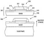
- FIG. 3illustrates another set of steps in fabricating the stacked non-volatile memory cells of the present invention.
- An oxide or other spacer material 300is formed over the just completed transistor from FIG. 2 .
- An oxide or other insulating layer 316is then formed over this and the above described process is repeated for as many transistor stacks as desired.
- the illustrated embodimentincludes forming the second transistor 301 over the transistor of FIG. 2 .
- the second transistor stackis comprised of the SiC or carbon rich silicon layer 315 over the oxide layer 316 .
- the source/drain regions 320 , 321formed in the SiC channel region layer 315 .
- the transistor stack 303comprising the ONO layer 310 and the control gate 311 is formed over the channel region layer 315 and the spacer material 312 , 313 is formed on either side of the transistor stack 303 .
- the carbon concentrationis decreased in each subsequently formed transistor layer.
- the lowest transistor layer 330will experience the greatest thermal budget. Therefore, the lowest layer 330 will have the greatest carbon content.
- the next layer of transistors 301will experience somewhat less thermal processing and, thus, has less carbon concentration than the lower layer.
- the decrease in carbon contentcontinues for each subsequently formed transistor layer.
- the carbon contentcan be tailored by changing the interstitial carbon concentration during Si:C growth. Such an embodiment provides a first channel layer with superior short channel effects at the cost of a slight mobility reduction.
- One embodiment of the above described stacked memory transistorsuses 4H—SiC in the SiC layer 103 .
- 4H SiChas a band gap energy of 3.26 eV, thermal conductivity of 3.0-3.8 W/cm K at 300K and a breakdown electric field of 2.2 ⁇ 10 6 V/cm.
- 6H—SiCthat has a band gap energy of 3.03 eV, thermal conductivity of 3.0-3.8 W/cm K at 300K and a breakdown electric field of 2.4 ⁇ 10 6 V/cm.
- FIG. 4illustrates a cross-sectional view of one embodiment of a three dimensional transistor in accordance with the thin film channel region layer of the present invention.
- the transistoris fabricated on an a-Si 400 layer on the substrate.
- the channel region 420 between the source/drain regions 403 , 404is a U-shaped region 420 that is formed in a thin layer of carbon rich silicon (Si:C).
- SiCmay be used for the channel region layer 401 .
- the ONO dielectric stack 410fills the U-shaped area.
- a poly or metal gate 411is formed over the ONO dielectric.
- the nitride layer of the ONO stack 410acts as the floating gate or charge storage layer.
- FIG. 4The fabrication of the embodiment of FIG. 4 can be repeated multiple times to form a transistor stack of such non-planar transistors. This process has been discussed previously. The various alternate embodiments in fabrication and materials discussed previously can also be employed in these non-planar transistors.
- FIG. 6illustrates another non-planar embodiment of the present invention.
- This embodimentis a FinFET memory cell that employs the SiC/Si:C thin film channel region layer of the present invention.
- the FinFET embodimentis comprised of a substrate 500 that, in one embodiment, is comprised of silicon.
- Two source/drain regions 501 , 502are formed in a three dimensional manner over the substrate 500 .
- a silicon “fin” 503is formed between the source/drain regions 501 , 502 .
- a gate 504is formed over the silicon “fin” 503 .
- the gatecan be a poly or metal gate. The gate is shown in dotted lines for purposes of clarity.
- the “fin” 503contains the Si:C/SiC channel region of the present invention.
- the structure of the “fin” 503is shown in FIG. 6 and described subsequently.
- the percentage of carbon added to the amorphous silicondecreases for each subsequently formed layer of vertically stacked FinFET memory cells.
- the FinFET of FIG. 5is a double or triple gate transistor.
- the transistoris a double gate if the gate oxide ( 601 of FIG. 6 ) between the gate 504 and the “fin” is greater on the sidewalls of the “fin” than the top.
- the transistoris a triple gate structure if the gate oxide is the same thickness on all three surfaces.
- FIG. 6shows a cross-sectional view, along axis A-A′, of the FinFET embodiment of FIG. 5 .
- This viewshows the substrate 500 over which the channel region 610 , the ONO layer 611 , and the Si:C or SiC thin film layer 503 is formed as shown in the three dimensional view of FIG. 5 .
- This viewadditionally shows the gate oxide layer 601 that is formed over the “fin”. While FIG. 6 shows this layer 601 to be of equal thickness over each surface, as would be the case in a triple gate structure, alternate embodiments can vary the thickness as previously described. For example, for a double gate device, the top surface of the “fin” would not be as thick as the sidewalls.
- the gate 504is formed over the gate oxide layer 601 .
- the gate 504can be comprised of polysilicon, metal, or some other suitable gate material.
- FIGS. 5 and 6can be repeated multiple times to form a three dimensional transistor stack, as illustrated in the embodiment of FIG. 3 , of such non-planar transistors. This process has been discussed previously. The various alternate embodiments in fabrication and materials discussed previously can also be employed in these non-planar transistors.
- FIG. 7illustrates a functional block diagram of a memory device 700 that can incorporate the stacked non-volatile memory cells of the present invention.
- the memory device 700is coupled to a processor 710 .
- the processor 710may be a microprocessor or some other type of controlling circuitry.
- the memory device 700 and the processor 710form part of an electronic memory system 720 .
- the memory device 700has been simplified to focus on features of the memory that are helpful in understanding the present invention.
- the memory deviceincludes an array of non-volatile memory cells 730 that can be floating gate flash memory cells.
- the memory array 730is arranged in banks of rows and columns.
- the control gates of each row of memory cellsis coupled with a word line while the drain regions of the memory cells are coupled to bit lines.
- the source regions of the memory cellsare coupled to source lines.
- the connection of the cells to the bit lines and source linesdepends on whether the array is a NAND architecture, a NOR architecture, an AND architecture or some other memory array architecture.
- the stacked non-volatile memory cells of the present inventioncan operate in any memory array architecture.
- An address buffer circuit 740is provided to latch address signals provided on address input connections A 0 -Ax 742 . Address signals are received and decoded by a row decoder 744 and a column decoder 746 to access the memory array 730 . It will be appreciated by those skilled in the art, with the benefit of the present description, that the number of address input connections depends on the density and architecture of the memory array 730 . That is, the number of addresses increases with both increased memory cell counts and increased bank and block counts.
- the memory integrated circuit 700reads data in the memory array 730 by sensing voltage or current changes in the memory array columns using sense/buffer circuitry 750 .
- the sense/buffer circuitryin one embodiment, is coupled to read and latch a row of data from the memory array 730 .
- Data input and output buffer circuitry 760is included for bi-directional data communication over a plurality of data connections 762 with the controller 710 .
- Write circuitry 755is provided to write data to the memory array.
- Control circuitry 770decodes signals provided on control connections 772 from the processor 710 . These signals are used to control the operations on the memory array 730 , including data read, data write, and erase operations.
- the control circuitry 770may be a state machine, a sequencer, or some other type of controller.
- the non-volatile memory device illustrated in FIG. 7has been simplified to facilitate a basic understanding of the features of the memory. A more detailed understanding of internal circuitry and functions of flash memories are known to those skilled in the art.
- FIG. 8is an illustration of an exemplary memory module 800 .
- Memory module 800is illustrated as a memory card, although the concepts discussed with reference to memory module 800 are applicable to other types of removable or portable memory, e.g., USB flash drives, and are intended to be within the scope of “memory module” as used herein.
- memory modulee.g., USB flash drives
- FIG. 8shows one example form factor, these concepts are applicable to other form factors as well.
- memory module 800will include a housing 805 (as depicted) to enclose one or more memory devices 810 , though such a housing is not essential to all devices or device applications. At least one memory device 810 is a non-volatile memory [including or adapted to perform elements of the invention].
- the housing 805includes one or more contacts 815 for communication with a host device. Examples of host devices include digital cameras, digital recording and playback devices, PDAs, personal computers, memory card readers, interface hubs and the like.
- the contacts 815are in the form of a standardized interface. For example, with a USB flash drive, the contacts 815 might be in the form of a USB Type-A male connector.
- the contacts 815are in the form of a semi-proprietary interface, such as might be found on COMPACTFLASH memory cards licensed by SANDISK Corporation, MEMORYSTICK memory cards licensed by SONY Corporation, SD SECURE DIGITAL memory cards licensed by TOSHIBA Corporation and the like. In general, however, contacts 815 provide an interface for passing control, address and/or data signals between the memory module 800 and a host having compatible receptors for the contacts 815 .
- the memory module 800may optionally include additional circuitry 820 which may be one or more integrated circuits and/or discrete components.
- the additional circuitry 820may include a memory controller for controlling access across multiple memory devices 810 and/or for providing a translation layer between an external host and a memory device 810 .
- a memory controllercould selectively couple an I/O connection (not shown in FIG. 8 ) of a memory device 810 to receive the appropriate signal at the appropriate I/O connection at the appropriate time or to provide the appropriate signal at the appropriate contact 815 at the appropriate time.
- the communication protocol between a host and the memory module 800may be different than what is required for access of a memory device 810 .
- a memory controllercould then translate the command sequences received from a host into the appropriate command sequences to achieve the desired access to the memory device 810 .
- Such translationmay further include changes in signal voltage levels in addition to command sequences.
- the additional circuitry 820may further include functionality unrelated to control of a memory device 810 such as logic functions as might be performed by an ASIC (application specific integrated circuit). Also, the additional circuitry 820 may include circuitry to restrict read or write access to the memory module 800 , such as password protection, biometrics or the like. The additional circuitry 820 may include circuitry to indicate a status of the memory module 800 . For example, the additional circuitry 820 may include functionality to determine whether power is being supplied to the memory module 800 and whether the memory module 800 is currently being accessed, and to display an indication of its status, such as a solid light while powered and a flashing light while being accessed. The additional circuitry 820 may further include passive devices, such as decoupling capacitors to help regulate power requirements within the memory module 800 .
- the non-volatile memory transistors of the present inventionare fabricated on a silicon carbide or carbon rich silicon channel thin film. This provides reduced tunnel barrier and ease of erase with lower voltages and electric fields.
- the cells of the present inventionare stackable in order to greatly increase the density of a memory device.
- the non-volatile memory cells of the present inventionmay be NAND-type cells, NOR-type cells, or any other type of non-volatile memory array architecture.
Landscapes
- Engineering & Computer Science (AREA)
- Physics & Mathematics (AREA)
- Condensed Matter Physics & Semiconductors (AREA)
- General Physics & Mathematics (AREA)
- Manufacturing & Machinery (AREA)
- Computer Hardware Design (AREA)
- Microelectronics & Electronic Packaging (AREA)
- Power Engineering (AREA)
- Non-Volatile Memory (AREA)
- Semiconductor Memories (AREA)
- Thin Film Transistor (AREA)
Abstract
Description
Claims (17)
Priority Applications (9)
| Application Number | Priority Date | Filing Date | Title |
|---|---|---|---|
| US11/377,158US7439594B2 (en) | 2006-03-16 | 2006-03-16 | Stacked non-volatile memory with silicon carbide-based amorphous silicon thin film transistors |
| JP2009500464AJP5051478B2 (en) | 2006-03-16 | 2007-03-15 | Stack nonvolatile memory having silicon carbide based amorphous silicon thin film transistor and method of manufacturing the same |
| CN200780009375.2ACN101405849B (en) | 2006-03-16 | 2007-03-15 | Stacked non-volatile memory with silicon carbide-based amorphous silicon thin-film transistors and method of manufacturing the same |
| PCT/US2007/006468WO2007109068A2 (en) | 2006-03-16 | 2007-03-15 | Stacked non-volatile memory with silicon-carbige-based amorphous-silicon thin-film transistors and manufacturing method thereof |
| KR1020087025338AKR100997350B1 (en) | 2006-03-16 | 2007-03-15 | Stacked nonvolatile memory with silicon carbide-based amorphous silicon thin film transistor and method of manufacturing same |
| US12/235,970US7994566B2 (en) | 2006-03-16 | 2008-09-23 | Stacked non-volatile memory with silicon carbide-based amorphous silicon finFETs |
| US13/186,822US8404536B2 (en) | 2006-03-16 | 2011-07-20 | Method for fabricating stacked non-volatile memory with silicon carbide-based amorphous silicon thin film transistors |
| US13/849,962US20130224923A1 (en) | 2006-03-16 | 2013-03-25 | Stacked non-volatile memory with silicon carbide-based amorphous silicon thin film transistors |
| US14/447,884US9111798B2 (en) | 2006-03-16 | 2014-07-31 | Memory with carbon-containing silicon channel |
Applications Claiming Priority (1)
| Application Number | Priority Date | Filing Date | Title |
|---|---|---|---|
| US11/377,158US7439594B2 (en) | 2006-03-16 | 2006-03-16 | Stacked non-volatile memory with silicon carbide-based amorphous silicon thin film transistors |
Related Child Applications (1)
| Application Number | Title | Priority Date | Filing Date |
|---|---|---|---|
| US12/235,970ContinuationUS7994566B2 (en) | 2006-03-16 | 2008-09-23 | Stacked non-volatile memory with silicon carbide-based amorphous silicon finFETs |
Publications (2)
| Publication Number | Publication Date |
|---|---|
| US20070215954A1 US20070215954A1 (en) | 2007-09-20 |
| US7439594B2true US7439594B2 (en) | 2008-10-21 |
Family
ID=38442501
Family Applications (5)
| Application Number | Title | Priority Date | Filing Date |
|---|---|---|---|
| US11/377,158Active2026-06-13US7439594B2 (en) | 2006-03-16 | 2006-03-16 | Stacked non-volatile memory with silicon carbide-based amorphous silicon thin film transistors |
| US12/235,970Active2026-04-07US7994566B2 (en) | 2006-03-16 | 2008-09-23 | Stacked non-volatile memory with silicon carbide-based amorphous silicon finFETs |
| US13/186,822ActiveUS8404536B2 (en) | 2006-03-16 | 2011-07-20 | Method for fabricating stacked non-volatile memory with silicon carbide-based amorphous silicon thin film transistors |
| US13/849,962AbandonedUS20130224923A1 (en) | 2006-03-16 | 2013-03-25 | Stacked non-volatile memory with silicon carbide-based amorphous silicon thin film transistors |
| US14/447,884ActiveUS9111798B2 (en) | 2006-03-16 | 2014-07-31 | Memory with carbon-containing silicon channel |
Family Applications After (4)
| Application Number | Title | Priority Date | Filing Date |
|---|---|---|---|
| US12/235,970Active2026-04-07US7994566B2 (en) | 2006-03-16 | 2008-09-23 | Stacked non-volatile memory with silicon carbide-based amorphous silicon finFETs |
| US13/186,822ActiveUS8404536B2 (en) | 2006-03-16 | 2011-07-20 | Method for fabricating stacked non-volatile memory with silicon carbide-based amorphous silicon thin film transistors |
| US13/849,962AbandonedUS20130224923A1 (en) | 2006-03-16 | 2013-03-25 | Stacked non-volatile memory with silicon carbide-based amorphous silicon thin film transistors |
| US14/447,884ActiveUS9111798B2 (en) | 2006-03-16 | 2014-07-31 | Memory with carbon-containing silicon channel |
Country Status (5)
| Country | Link |
|---|---|
| US (5) | US7439594B2 (en) |
| JP (1) | JP5051478B2 (en) |
| KR (1) | KR100997350B1 (en) |
| CN (1) | CN101405849B (en) |
| WO (1) | WO2007109068A2 (en) |
Cited By (5)
| Publication number | Priority date | Publication date | Assignee | Title |
|---|---|---|---|---|
| US20060197137A1 (en)* | 2004-07-28 | 2006-09-07 | Chandra Mouli | Memory devices, transistors, memory cells, and methods of making same |
| US20070262353A1 (en)* | 2006-04-28 | 2007-11-15 | Nobuyasu Nishiyama | Semiconductor device and method of fabricating the same |
| US20100320536A1 (en)* | 2009-06-17 | 2010-12-23 | Infineon Technologies Austria Ag | Transistor component having an amorphous semi-isolating channel control layer |
| US20140054724A1 (en)* | 2012-08-24 | 2014-02-27 | Taiwan Semiconductor Manufacturing Company Limited | Aligned gate-all-around structure |
| US8866227B2 (en) | 2011-10-25 | 2014-10-21 | International Business Machines Corporation | Thin semiconductor-on-insulator MOSFET with co-integrated silicon, silicon germanium and silicon doped with carbon channels |
Families Citing this family (84)
| Publication number | Priority date | Publication date | Assignee | Title |
|---|---|---|---|---|
| JP4490927B2 (en)* | 2006-01-24 | 2010-06-30 | 株式会社東芝 | Semiconductor device |
| JP2007317920A (en)* | 2006-05-26 | 2007-12-06 | Toshiba Corp | Semiconductor memory device and manufacturing method thereof |
| US8159868B2 (en)* | 2008-08-22 | 2012-04-17 | Zeno Semiconductor, Inc. | Semiconductor memory having both volatile and non-volatile functionality including resistance change material and method of operating |
| US9601493B2 (en) | 2006-11-29 | 2017-03-21 | Zeno Semiconductor, Inc | Compact semiconductor memory device having reduced number of contacts, methods of operating and methods of making |
| US8194451B2 (en) | 2007-11-29 | 2012-06-05 | Zeno Semiconductor, Inc. | Memory cells, memory cell arrays, methods of using and methods of making |
| US7760548B2 (en) | 2006-11-29 | 2010-07-20 | Yuniarto Widjaja | Semiconductor memory having both volatile and non-volatile functionality and method of operating |
| US8547756B2 (en) | 2010-10-04 | 2013-10-01 | Zeno Semiconductor, Inc. | Semiconductor memory device having an electrically floating body transistor |
| US9391079B2 (en) | 2007-11-29 | 2016-07-12 | Zeno Semiconductor, Inc. | Compact semiconductor memory device having reduced number of contacts, methods of operating and methods of making |
| US8077536B2 (en) | 2008-08-05 | 2011-12-13 | Zeno Semiconductor, Inc. | Method of operating semiconductor memory device with floating body transistor using silicon controlled rectifier principle |
| US8514622B2 (en)* | 2007-11-29 | 2013-08-20 | Zeno Semiconductor, Inc. | Compact semiconductor memory device having reduced number of contacts, methods of operating and methods of making |
| US7859081B2 (en)* | 2007-03-29 | 2010-12-28 | Intel Corporation | Capacitor, method of increasing a capacitance area of same, and system containing same |
| US9230651B2 (en) | 2012-04-08 | 2016-01-05 | Zeno Semiconductor, Inc. | Memory device having electrically floating body transitor |
| US8614124B2 (en) | 2007-05-25 | 2013-12-24 | Cypress Semiconductor Corporation | SONOS ONO stack scaling |
| US9299568B2 (en) | 2007-05-25 | 2016-03-29 | Cypress Semiconductor Corporation | SONOS ONO stack scaling |
| TWI351767B (en)* | 2007-10-02 | 2011-11-01 | Nanya Technology Corp | Two-bit flash memory |
| US8059459B2 (en) | 2007-10-24 | 2011-11-15 | Zeno Semiconductor, Inc. | Semiconductor memory having both volatile and non-volatile functionality and method of operating |
| US10403361B2 (en) | 2007-11-29 | 2019-09-03 | Zeno Semiconductor, Inc. | Memory cells, memory cell arrays, methods of using and methods of making |
| US8264875B2 (en) | 2010-10-04 | 2012-09-11 | Zeno Semiconducor, Inc. | Semiconductor memory device having an electrically floating body transistor |
| US8130548B2 (en) | 2007-11-29 | 2012-03-06 | Zeno Semiconductor, Inc. | Semiconductor memory having electrically floating body transistor |
| US8130547B2 (en) | 2007-11-29 | 2012-03-06 | Zeno Semiconductor, Inc. | Method of maintaining the state of semiconductor memory having electrically floating body transistor |
| US8174886B2 (en) | 2007-11-29 | 2012-05-08 | Zeno Semiconductor, Inc. | Semiconductor memory having electrically floating body transistor |
| WO2009072984A1 (en)* | 2007-12-07 | 2009-06-11 | Agency For Science, Technology And Research | A silicon-germanium nanowire structure and a method of forming the same |
| US9431549B2 (en) | 2007-12-12 | 2016-08-30 | Cypress Semiconductor Corporation | Nonvolatile charge trap memory device having a high dielectric constant blocking region |
| US8014200B2 (en) | 2008-04-08 | 2011-09-06 | Zeno Semiconductor, Inc. | Semiconductor memory having volatile and multi-bit, non-volatile functionality and methods of operating |
| USRE47381E1 (en) | 2008-09-03 | 2019-05-07 | Zeno Semiconductor, Inc. | Forming semiconductor cells with regions of varying conductivity |
| US11908899B2 (en) | 2009-02-20 | 2024-02-20 | Zeno Semiconductor, Inc. | MOSFET and memory cell having improved drain current through back bias application |
| WO2016176248A1 (en) | 2015-04-29 | 2016-11-03 | Zeno Semiconductor, Inc. | A mosfet and memory cell having improved drain current through back bias application |
| US8071453B1 (en) | 2009-04-24 | 2011-12-06 | Cypress Semiconductor Corporation | Method of ONO integration into MOS flow |
| US9102522B2 (en) | 2009-04-24 | 2015-08-11 | Cypress Semiconductor Corporation | Method of ONO integration into logic CMOS flow |
| US8183617B2 (en)* | 2009-04-27 | 2012-05-22 | Macronix International Co., Ltd. | Injection method with Schottky source/drain |
| US8461640B2 (en) | 2009-09-08 | 2013-06-11 | Silicon Storage Technology, Inc. | FIN-FET non-volatile memory cell, and an array and method of manufacturing |
| IN2012DN06399A (en) | 2010-02-07 | 2015-10-02 | Zeno Semiconductor Inc | |
| US9646869B2 (en) | 2010-03-02 | 2017-05-09 | Micron Technology, Inc. | Semiconductor devices including a diode structure over a conductive strap and methods of forming such semiconductor devices |
| US9922981B2 (en) | 2010-03-02 | 2018-03-20 | Zeno Semiconductor, Inc. | Compact semiconductor memory device having reduced number of contacts, methods of operating and methods of making |
| US8513722B2 (en) | 2010-03-02 | 2013-08-20 | Micron Technology, Inc. | Floating body cell structures, devices including same, and methods for forming same |
| US9608119B2 (en)* | 2010-03-02 | 2017-03-28 | Micron Technology, Inc. | Semiconductor-metal-on-insulator structures, methods of forming such structures, and semiconductor devices including such structures |
| US8507966B2 (en)* | 2010-03-02 | 2013-08-13 | Micron Technology, Inc. | Semiconductor cells, arrays, devices and systems having a buried conductive line and methods for forming the same |
| US8288795B2 (en) | 2010-03-02 | 2012-10-16 | Micron Technology, Inc. | Thyristor based memory cells, devices and systems including the same and methods for forming the same |
| US10340276B2 (en) | 2010-03-02 | 2019-07-02 | Zeno Semiconductor, Inc. | Method of maintaining the state of semiconductor memory having electrically floating body transistor |
| US10461084B2 (en) | 2010-03-02 | 2019-10-29 | Zeno Semiconductor, Inc. | Compact semiconductor memory device having reduced number of contacts, methods of operating and methods of making |
| AU2011222601B2 (en)* | 2010-03-04 | 2013-09-26 | University Of Florida Research Foundation Inc. | Semiconductor devices including an electrically percolating source layer and methods of fabricating the same |
| US8355281B2 (en)* | 2010-04-20 | 2013-01-15 | Micron Technology, Inc. | Flash memory having multi-level architecture |
| US8582359B2 (en) | 2010-11-16 | 2013-11-12 | Zeno Semiconductor, Inc. | Dual-port semiconductor memory and first-in first-out (FIFO) memory having electrically floating body transistor |
| JP2012146817A (en)* | 2011-01-12 | 2012-08-02 | Toshiba Corp | Semiconductor device and method of manufacturing the same |
| US8598621B2 (en) | 2011-02-11 | 2013-12-03 | Micron Technology, Inc. | Memory cells, memory arrays, methods of forming memory cells, and methods of forming a shared doped semiconductor region of a vertically oriented thyristor and a vertically oriented access transistor |
| US8952418B2 (en) | 2011-03-01 | 2015-02-10 | Micron Technology, Inc. | Gated bipolar junction transistors |
| US8519431B2 (en) | 2011-03-08 | 2013-08-27 | Micron Technology, Inc. | Thyristors |
| US8957458B2 (en) | 2011-03-24 | 2015-02-17 | Zeno Semiconductor, Inc. | Asymmetric semiconductor memory device having electrically floating body transistor |
| US8772848B2 (en) | 2011-07-26 | 2014-07-08 | Micron Technology, Inc. | Circuit structures, memory circuitry, and methods |
| US9025358B2 (en) | 2011-10-13 | 2015-05-05 | Zeno Semiconductor Inc | Semiconductor memory having both volatile and non-volatile functionality comprising resistive change material and method of operating |
| US9230814B2 (en)* | 2011-10-28 | 2016-01-05 | Invensas Corporation | Non-volatile memory devices having vertical drain to gate capacitive coupling |
| CN107331416B (en) | 2012-02-16 | 2020-11-10 | 芝诺半导体有限公司 | Memory cell including primary and secondary transistors |
| EP2831918A4 (en)* | 2012-03-29 | 2015-11-18 | Cypress Semiconductor Corp | ONO INTEGRATION METHOD IN LOGICAL CMOS FLOW |
| WO2014071343A1 (en) | 2012-11-05 | 2014-05-08 | University Of Florida Research Foundation, Inc. | Brightness compensation in a display |
| CN104137266B (en)* | 2012-12-27 | 2015-07-15 | 松下电器产业株式会社 | Silicon carbide semiconductor device and method for manufacturing same |
| US9208880B2 (en) | 2013-01-14 | 2015-12-08 | Zeno Semiconductor, Inc. | Content addressable memory device having electrically floating body transistor |
| US9029922B2 (en) | 2013-03-09 | 2015-05-12 | Zeno Semiconductor, Inc. | Memory device comprising electrically floating body transistor |
| US9275723B2 (en) | 2013-04-10 | 2016-03-01 | Zeno Semiconductor, Inc. | Scalable floating body memory cell for memory compilers and method of using floating body memories with memory compilers |
| WO2014174937A1 (en)* | 2013-04-24 | 2014-10-30 | 独立行政法人産業技術総合研究所 | Semiconductor device having heterogeneous material connection |
| US9368625B2 (en) | 2013-05-01 | 2016-06-14 | Zeno Semiconductor, Inc. | NAND string utilizing floating body memory cell |
| US9281022B2 (en) | 2013-07-10 | 2016-03-08 | Zeno Semiconductor, Inc. | Systems and methods for reducing standby power in floating body memory devices |
| DE102013215932B3 (en) | 2013-08-12 | 2015-02-19 | Rosenberger Hochfrequenztechnik Gmbh & Co. Kg | Measuring device with remote control |
| US9240420B2 (en)* | 2013-09-06 | 2016-01-19 | Sandisk Technologies Inc. | 3D non-volatile storage with wide band gap transistor decoder |
| US9136355B2 (en)* | 2013-12-03 | 2015-09-15 | Intermolecular, Inc. | Methods for forming amorphous silicon thin film transistors |
| US9548119B2 (en) | 2014-01-15 | 2017-01-17 | Zeno Semiconductor, Inc | Memory device comprising an electrically floating body transistor |
| US9431537B2 (en) | 2014-03-26 | 2016-08-30 | Samsung Electronics Co., Ltd. | Semiconductor devices and methods of fabricating the same |
| US9496053B2 (en) | 2014-08-15 | 2016-11-15 | Zeno Semiconductor, Inc. | Memory device comprising electrically floating body transistor |
| US9548362B2 (en) | 2014-10-10 | 2017-01-17 | Taiwan Semiconductor Manufacturing Company, Ltd. | High mobility devices with anti-punch through layers and methods of forming same |
| US10553683B2 (en) | 2015-04-29 | 2020-02-04 | Zeno Semiconductor, Inc. | MOSFET and memory cell having improved drain current through back bias application |
| US9799776B2 (en) | 2015-06-15 | 2017-10-24 | Stmicroelectronics, Inc. | Semi-floating gate FET |
| CN107646137B (en)* | 2015-06-23 | 2022-03-08 | 英特尔公司 | Stackable thin film memory |
| EP3353810A4 (en)* | 2015-09-25 | 2019-05-01 | Intel Corporation | PASSIVATION OF TRANSISTOR CHANNEL ZONE INTERFACES |
| US9646886B1 (en) | 2015-12-30 | 2017-05-09 | International Business Machines Corporation | Tailored silicon layers for transistor multi-gate control |
| US10127979B2 (en) | 2016-03-11 | 2018-11-13 | Western Digital Technologies, Inc. | Memory cell located pulse generator |
| US10381408B2 (en) | 2016-03-24 | 2019-08-13 | Western Digital Technologies, Inc. | Method to fabricate discrete vertical transistors |
| US10079301B2 (en) | 2016-11-01 | 2018-09-18 | Zeno Semiconductor, Inc. | Memory device comprising an electrically floating body transistor and methods of using |
| JP2019041054A (en)* | 2017-08-28 | 2019-03-14 | 東芝メモリ株式会社 | Semiconductor device |
| WO2019125362A1 (en)* | 2017-12-18 | 2019-06-27 | Intel Corporation | High mobility oxide thin film transistor |
| TWI787498B (en) | 2018-04-18 | 2022-12-21 | 美商季諾半導體股份有限公司 | A memory device comprising an electrically floating body transistor |
| FR3086101B1 (en)* | 2018-09-17 | 2022-07-08 | Ion Beam Services | DEVICE FOR ENHANCING CARRIER MOBILITY IN A MOSFET CHANNEL ON SILICON CARBIDE |
| WO2020076652A1 (en)* | 2018-10-09 | 2020-04-16 | Micron Technology, Inc. | Semiconductor devices comprising transistors having increased threshold voltage and related methods and systems |
| US11600663B2 (en) | 2019-01-11 | 2023-03-07 | Zeno Semiconductor, Inc. | Memory cell and memory array select transistor |
| US12439611B2 (en) | 2019-03-12 | 2025-10-07 | Zeno Semiconductor, Inc. | Memory cell and memory array select transistor |
| US11653488B2 (en) | 2020-05-07 | 2023-05-16 | Micron Technology, Inc. | Apparatuses including transistors, and related methods, memory devices, and electronic systems |
Citations (18)
| Publication number | Priority date | Publication date | Assignee | Title |
|---|---|---|---|---|
| US5888857A (en) | 1992-12-04 | 1999-03-30 | Semiconductor Energy Laboratory Co., Ltd. | Semiconductor device and method for manufacturing the same |
| US6184068B1 (en) | 1994-06-02 | 2001-02-06 | Semiconductor Energy Laboratory Co., Ltd. | Process for fabricating semiconductor device |
| US6232156B1 (en) | 1994-02-03 | 2001-05-15 | Semiconductor Energy Laboratory Co., Ltd. | Method of manufacturing a semiconductor device |
| US6297173B1 (en) | 1997-08-05 | 2001-10-02 | Motorola, Inc. | Process for forming a semiconductor device |
| WO2003017285A1 (en) | 2001-08-13 | 2003-02-27 | Matrix Semiconductor, Inc. | Nonvolatile memory on soi and compound semiconductor substrates and methods of fabrication |
| US20030170930A1 (en)* | 2002-02-09 | 2003-09-11 | Samsung Electronics Co., Ltd. | Memory device utilizing carbon nanotubes and method of fabricating the memory device |
| US6674138B1 (en) | 2001-12-31 | 2004-01-06 | Advanced Micro Devices, Inc. | Use of high-k dielectric materials in modified ONO structure for semiconductor devices |
| US6806125B2 (en) | 1992-12-04 | 2004-10-19 | Semiconductor Energy Laboratory Co., Ltd. | Method of manufacturing a thin film transistor device |
| US20040207001A1 (en) | 2001-03-28 | 2004-10-21 | Matrix Semiconductor, Inc. | Two mask floating gate EEPROM and method of making |
| US6822262B2 (en) | 1997-07-23 | 2004-11-23 | Semiconductor Energy Laboratory Co., Ltd. | Semiconductor thin film and semiconductor device |
| US6841813B2 (en)* | 2001-08-13 | 2005-01-11 | Matrix Semiconductor, Inc. | TFT mask ROM and method for making same |
| US20050036382A1 (en) | 2002-12-18 | 2005-02-17 | Semiconductor Energy Laboratory Co., Ltd. | Semiconductor memory element, semiconductor memory device and method of fabricating the same |
| US20050263767A1 (en) | 2004-05-28 | 2005-12-01 | Semiconductor Energy Laboratory Co., Ltd. | Semiconductor device and method for manufacturing the same |
| US20050280001A1 (en)* | 2004-06-22 | 2005-12-22 | Chang Peter L | Memory cell using silicon carbide |
| US20060018164A1 (en)* | 2004-02-18 | 2006-01-26 | Koucheng Wu | Nor-type channel-program channel-erase contactless flash memory on SOI |
| US20060024868A1 (en)* | 2003-12-18 | 2006-02-02 | Matrix Semiconductor, Inc. | Selective oxidation of silicon in diode, TFT, and monolithic three dimensional memory arrays |
| US20060194379A1 (en)* | 2003-07-28 | 2006-08-31 | Jun Suda | Field effect transistor and method for manufacturing same |
| US20060197141A1 (en)* | 2005-02-23 | 2006-09-07 | Klaus-Dieter Ufert | Charge trapping semiconductor memory element with improved trapping dielectric |
Family Cites Families (17)
| Publication number | Priority date | Publication date | Assignee | Title |
|---|---|---|---|---|
| US4849797A (en)* | 1987-01-23 | 1989-07-18 | Hosiden Electronics Co., Ltd. | Thin film transistor |
| JPH0590602A (en)* | 1991-09-30 | 1993-04-09 | Rohm Co Ltd | Semiconductor memory cell and manufacture thereof |
| JPH05145078A (en)* | 1991-11-22 | 1993-06-11 | Kawasaki Steel Corp | Semiconductor nonvolatile storage element and manufacture thereof |
| JPH0773116B2 (en)* | 1994-04-08 | 1995-08-02 | 工業技術院長 | Non-volatile semiconductor memory device |
| JPH0964209A (en)* | 1995-08-25 | 1997-03-07 | Toshiba Corp | Semiconductor device and manufacturing method thereof |
| US6607948B1 (en)* | 1998-12-24 | 2003-08-19 | Kabushiki Kaisha Toshiba | Method of manufacturing a substrate using an SiGe layer |
| DE10204873C1 (en)* | 2002-02-06 | 2003-10-09 | Infineon Technologies Ag | Manufacturing process for memory cell |
| JP4498685B2 (en)* | 2002-03-22 | 2010-07-07 | 株式会社半導体エネルギー研究所 | Method for manufacturing semiconductor memory element |
| US7358121B2 (en)* | 2002-08-23 | 2008-04-15 | Intel Corporation | Tri-gate devices and methods of fabrication |
| KR100474850B1 (en) | 2002-11-15 | 2005-03-11 | 삼성전자주식회사 | Silicon/Oxide/Nitride/Oxide/Silicon nonvolatile memory with vertical channel and Fabricating method thereof |
| US6844238B2 (en)* | 2003-03-26 | 2005-01-18 | Taiwan Semiconductor Manufacturing Co., Ltd | Multiple-gate transistors with improved gate control |
| JP2007517386A (en)* | 2003-12-19 | 2007-06-28 | インフィネオン テクノロジーズ アクチエンゲゼルシャフト | BRIDGE FIELD EFFECT TRANSISTOR MEMORY CELL, DEVICE HAVING THE CELL, AND METHOD FOR MANUFACTURING BRIDGE FIELD EFFECT TRANSISTOR MEMORY CELL |
| JP3910971B2 (en)* | 2004-03-26 | 2007-04-25 | 株式会社東芝 | Field effect transistor |
| KR100625175B1 (en)* | 2004-05-25 | 2006-09-20 | 삼성전자주식회사 | Semiconductor device having channel layer and method of manufacturing same |
| US7106625B2 (en)* | 2004-07-06 | 2006-09-12 | Macronix International Co, Td | Charge trapping non-volatile memory with two trapping locations per gate, and method for operating same |
| KR100555569B1 (en)* | 2004-08-06 | 2006-03-03 | 삼성전자주식회사 | A semiconductor device having a channel region limited by an insulating film and its manufacturing method |
| US7602006B2 (en)* | 2005-04-20 | 2009-10-13 | Taiwan Semiconductor Manufacturing Co., Ltd. | Semiconductor flash device |
- 2006
- 2006-03-16USUS11/377,158patent/US7439594B2/enactiveActive
- 2007
- 2007-03-15CNCN200780009375.2Apatent/CN101405849B/ennot_activeExpired - Fee Related
- 2007-03-15WOPCT/US2007/006468patent/WO2007109068A2/enactiveApplication Filing
- 2007-03-15KRKR1020087025338Apatent/KR100997350B1/ennot_activeExpired - Fee Related
- 2007-03-15JPJP2009500464Apatent/JP5051478B2/enactiveActive
- 2008
- 2008-09-23USUS12/235,970patent/US7994566B2/enactiveActive
- 2011
- 2011-07-20USUS13/186,822patent/US8404536B2/enactiveActive
- 2013
- 2013-03-25USUS13/849,962patent/US20130224923A1/ennot_activeAbandoned
- 2014
- 2014-07-31USUS14/447,884patent/US9111798B2/enactiveActive
Patent Citations (18)
| Publication number | Priority date | Publication date | Assignee | Title |
|---|---|---|---|---|
| US6806125B2 (en) | 1992-12-04 | 2004-10-19 | Semiconductor Energy Laboratory Co., Ltd. | Method of manufacturing a thin film transistor device |
| US5888857A (en) | 1992-12-04 | 1999-03-30 | Semiconductor Energy Laboratory Co., Ltd. | Semiconductor device and method for manufacturing the same |
| US6232156B1 (en) | 1994-02-03 | 2001-05-15 | Semiconductor Energy Laboratory Co., Ltd. | Method of manufacturing a semiconductor device |
| US6184068B1 (en) | 1994-06-02 | 2001-02-06 | Semiconductor Energy Laboratory Co., Ltd. | Process for fabricating semiconductor device |
| US6822262B2 (en) | 1997-07-23 | 2004-11-23 | Semiconductor Energy Laboratory Co., Ltd. | Semiconductor thin film and semiconductor device |
| US6297173B1 (en) | 1997-08-05 | 2001-10-02 | Motorola, Inc. | Process for forming a semiconductor device |
| US20040207001A1 (en) | 2001-03-28 | 2004-10-21 | Matrix Semiconductor, Inc. | Two mask floating gate EEPROM and method of making |
| WO2003017285A1 (en) | 2001-08-13 | 2003-02-27 | Matrix Semiconductor, Inc. | Nonvolatile memory on soi and compound semiconductor substrates and methods of fabrication |
| US6841813B2 (en)* | 2001-08-13 | 2005-01-11 | Matrix Semiconductor, Inc. | TFT mask ROM and method for making same |
| US6674138B1 (en) | 2001-12-31 | 2004-01-06 | Advanced Micro Devices, Inc. | Use of high-k dielectric materials in modified ONO structure for semiconductor devices |
| US20030170930A1 (en)* | 2002-02-09 | 2003-09-11 | Samsung Electronics Co., Ltd. | Memory device utilizing carbon nanotubes and method of fabricating the memory device |
| US20050036382A1 (en) | 2002-12-18 | 2005-02-17 | Semiconductor Energy Laboratory Co., Ltd. | Semiconductor memory element, semiconductor memory device and method of fabricating the same |
| US20060194379A1 (en)* | 2003-07-28 | 2006-08-31 | Jun Suda | Field effect transistor and method for manufacturing same |
| US20060024868A1 (en)* | 2003-12-18 | 2006-02-02 | Matrix Semiconductor, Inc. | Selective oxidation of silicon in diode, TFT, and monolithic three dimensional memory arrays |
| US20060018164A1 (en)* | 2004-02-18 | 2006-01-26 | Koucheng Wu | Nor-type channel-program channel-erase contactless flash memory on SOI |
| US20050263767A1 (en) | 2004-05-28 | 2005-12-01 | Semiconductor Energy Laboratory Co., Ltd. | Semiconductor device and method for manufacturing the same |
| US20050280001A1 (en)* | 2004-06-22 | 2005-12-22 | Chang Peter L | Memory cell using silicon carbide |
| US20060197141A1 (en)* | 2005-02-23 | 2006-09-07 | Klaus-Dieter Ufert | Charge trapping semiconductor memory element with improved trapping dielectric |
Non-Patent Citations (2)
| Title |
|---|
| Cheng, Kuo-Liang et al. "RAMSES-FT: A Fault Simulator for Flash Memory Testing and Diagnostics." Proceedings of the 20th IEEE VLSI Test Symposium. 2002.* |
| Chevaleevski, Oleg et al, "ESR Studies of Hydrogenated Nanocrystalline Silicon Carbide." 3rd World Conference on Photovoltaic Energy Conversion, pp. 1859-1862. May 11-18, 2003.* |
Cited By (15)
| Publication number | Priority date | Publication date | Assignee | Title |
|---|---|---|---|---|
| US8080837B2 (en) | 2004-07-28 | 2011-12-20 | Micron Technology, Inc. | Memory devices, transistors, and memory cells |
| US8703566B2 (en) | 2004-07-28 | 2014-04-22 | Micron Technology, Inc. | Transistors comprising a SiC-containing channel |
| US8470666B2 (en) | 2004-07-28 | 2013-06-25 | Micron Technology, Inc. | Methods of making random access memory devices, transistors, and memory cells |
| US20060197137A1 (en)* | 2004-07-28 | 2006-09-07 | Chandra Mouli | Memory devices, transistors, memory cells, and methods of making same |
| US8415722B2 (en) | 2004-07-28 | 2013-04-09 | Micron Technology, Inc. | Memory devices and memory cells |
| US20100151645A1 (en)* | 2006-04-28 | 2010-06-17 | Kabushiki Kaisha Toshiba | Semiconductor device and method of fabricating the same |
| US8062938B2 (en) | 2006-04-28 | 2011-11-22 | Kabushiki Kaisha Toshiba | Semiconductor device and method of fabricating the same |
| US7683436B2 (en)* | 2006-04-28 | 2010-03-23 | Kabushiki Kaisha Toshiba | Semiconductor device having a pole-shaped portion and method of fabricating the same |
| US20070262353A1 (en)* | 2006-04-28 | 2007-11-15 | Nobuyasu Nishiyama | Semiconductor device and method of fabricating the same |
| US20100320536A1 (en)* | 2009-06-17 | 2010-12-23 | Infineon Technologies Austria Ag | Transistor component having an amorphous semi-isolating channel control layer |
| US8735981B2 (en)* | 2009-06-17 | 2014-05-27 | Infineon Technologies Austria Ag | Transistor component having an amorphous semi-isolating channel control layer |
| US8866227B2 (en) | 2011-10-25 | 2014-10-21 | International Business Machines Corporation | Thin semiconductor-on-insulator MOSFET with co-integrated silicon, silicon germanium and silicon doped with carbon channels |
| US20140054724A1 (en)* | 2012-08-24 | 2014-02-27 | Taiwan Semiconductor Manufacturing Company Limited | Aligned gate-all-around structure |
| US9006829B2 (en)* | 2012-08-24 | 2015-04-14 | Taiwan Semiconductor Manufacturing Company, Ltd. | Aligned gate-all-around structure |
| US9412828B2 (en) | 2012-08-24 | 2016-08-09 | Taiwan Semiconductor Manufacturing Company, Ltd. | Aligned gate-all-around structure |
Also Published As
| Publication number | Publication date |
|---|---|
| US7994566B2 (en) | 2011-08-09 |
| JP5051478B2 (en) | 2012-10-17 |
| US20140339572A1 (en) | 2014-11-20 |
| JP2009530820A (en) | 2009-08-27 |
| US20110275182A1 (en) | 2011-11-10 |
| WO2007109068A2 (en) | 2007-09-27 |
| KR20080114806A (en) | 2008-12-31 |
| US8404536B2 (en) | 2013-03-26 |
| KR100997350B1 (en) | 2010-11-29 |
| US20090039357A1 (en) | 2009-02-12 |
| CN101405849A (en) | 2009-04-08 |
| CN101405849B (en) | 2011-03-30 |
| US20130224923A1 (en) | 2013-08-29 |
| WO2007109068A3 (en) | 2008-01-31 |
| US9111798B2 (en) | 2015-08-18 |
| US20070215954A1 (en) | 2007-09-20 |
Similar Documents
| Publication | Publication Date | Title |
|---|---|---|
| US7439594B2 (en) | Stacked non-volatile memory with silicon carbide-based amorphous silicon thin film transistors | |
| US7772066B2 (en) | DRAM tunneling access transistor | |
| WO2007070424A1 (en) | Enhanced multi-bit non-volatile memory device with resonant tunnel barrier | |
| US12274057B2 (en) | Methods of forming integrated circuit structures comprising isolation structures with different depths | |
| US11756624B2 (en) | Methods of forming transistors having raised extension regions | |
| US20070045706A1 (en) | Combined volatile and non-volatile memory device with graded composition insulator stack | |
| US20250267860A1 (en) | Apparatus having transistors with raised extension regions and semiconductor fins | |
| US7253469B2 (en) | Flash memory device having a graded composition, high dielectric constant gate insulator | |
| US20210408244A1 (en) | Field-effect transistors and methods of their formation | |
| JP5351274B2 (en) | Nonvolatile semiconductor memory device | |
| CN114188336B (en) | Memory structure and operation method thereof | |
| TW513789B (en) | Manufacturing method of flash memory with floating gate, control gate and erase gate | |
| US20060003516A1 (en) | Flash memory devices on silicon carbide |
Legal Events
| Date | Code | Title | Description |
|---|---|---|---|
| AS | Assignment | Owner name:MICRON TECHNOLOGY, INC., IDAHO Free format text:ASSIGNMENT OF ASSIGNORS INTEREST;ASSIGNOR:MOULI, CHANDRA;REEL/FRAME:017652/0780 Effective date:20060309 | |
| FEPP | Fee payment procedure | Free format text:PAYOR NUMBER ASSIGNED (ORIGINAL EVENT CODE: ASPN); ENTITY STATUS OF PATENT OWNER: LARGE ENTITY | |
| STCF | Information on status: patent grant | Free format text:PATENTED CASE | |
| CC | Certificate of correction | ||
| FPAY | Fee payment | Year of fee payment:4 | |
| FPAY | Fee payment | Year of fee payment:8 | |
| AS | Assignment | Owner name:U.S. BANK NATIONAL ASSOCIATION, AS COLLATERAL AGENT, CALIFORNIA Free format text:SECURITY INTEREST;ASSIGNOR:MICRON TECHNOLOGY, INC.;REEL/FRAME:038669/0001 Effective date:20160426 Owner name:U.S. BANK NATIONAL ASSOCIATION, AS COLLATERAL AGEN Free format text:SECURITY INTEREST;ASSIGNOR:MICRON TECHNOLOGY, INC.;REEL/FRAME:038669/0001 Effective date:20160426 | |
| AS | Assignment | Owner name:MORGAN STANLEY SENIOR FUNDING, INC., AS COLLATERAL AGENT, MARYLAND Free format text:PATENT SECURITY AGREEMENT;ASSIGNOR:MICRON TECHNOLOGY, INC.;REEL/FRAME:038954/0001 Effective date:20160426 Owner name:MORGAN STANLEY SENIOR FUNDING, INC., AS COLLATERAL Free format text:PATENT SECURITY AGREEMENT;ASSIGNOR:MICRON TECHNOLOGY, INC.;REEL/FRAME:038954/0001 Effective date:20160426 | |
| AS | Assignment | Owner name:U.S. BANK NATIONAL ASSOCIATION, AS COLLATERAL AGENT, CALIFORNIA Free format text:CORRECTIVE ASSIGNMENT TO CORRECT THE REPLACE ERRONEOUSLY FILED PATENT #7358718 WITH THE CORRECT PATENT #7358178 PREVIOUSLY RECORDED ON REEL 038669 FRAME 0001. ASSIGNOR(S) HEREBY CONFIRMS THE SECURITY INTEREST;ASSIGNOR:MICRON TECHNOLOGY, INC.;REEL/FRAME:043079/0001 Effective date:20160426 Owner name:U.S. BANK NATIONAL ASSOCIATION, AS COLLATERAL AGEN Free format text:CORRECTIVE ASSIGNMENT TO CORRECT THE REPLACE ERRONEOUSLY FILED PATENT #7358718 WITH THE CORRECT PATENT #7358178 PREVIOUSLY RECORDED ON REEL 038669 FRAME 0001. ASSIGNOR(S) HEREBY CONFIRMS THE SECURITY INTEREST;ASSIGNOR:MICRON TECHNOLOGY, INC.;REEL/FRAME:043079/0001 Effective date:20160426 | |
| AS | Assignment | Owner name:JPMORGAN CHASE BANK, N.A., AS COLLATERAL AGENT, ILLINOIS Free format text:SECURITY INTEREST;ASSIGNORS:MICRON TECHNOLOGY, INC.;MICRON SEMICONDUCTOR PRODUCTS, INC.;REEL/FRAME:047540/0001 Effective date:20180703 Owner name:JPMORGAN CHASE BANK, N.A., AS COLLATERAL AGENT, IL Free format text:SECURITY INTEREST;ASSIGNORS:MICRON TECHNOLOGY, INC.;MICRON SEMICONDUCTOR PRODUCTS, INC.;REEL/FRAME:047540/0001 Effective date:20180703 | |
| AS | Assignment | Owner name:MICRON TECHNOLOGY, INC., IDAHO Free format text:RELEASE BY SECURED PARTY;ASSIGNOR:U.S. BANK NATIONAL ASSOCIATION, AS COLLATERAL AGENT;REEL/FRAME:047243/0001 Effective date:20180629 | |
| AS | Assignment | Owner name:MICRON TECHNOLOGY, INC., IDAHO Free format text:RELEASE BY SECURED PARTY;ASSIGNOR:MORGAN STANLEY SENIOR FUNDING, INC., AS COLLATERAL AGENT;REEL/FRAME:050937/0001 Effective date:20190731 | |
| AS | Assignment | Owner name:MICRON TECHNOLOGY, INC., IDAHO Free format text:RELEASE BY SECURED PARTY;ASSIGNOR:JPMORGAN CHASE BANK, N.A., AS COLLATERAL AGENT;REEL/FRAME:051028/0001 Effective date:20190731 Owner name:MICRON SEMICONDUCTOR PRODUCTS, INC., IDAHO Free format text:RELEASE BY SECURED PARTY;ASSIGNOR:JPMORGAN CHASE BANK, N.A., AS COLLATERAL AGENT;REEL/FRAME:051028/0001 Effective date:20190731 | |
| MAFP | Maintenance fee payment | Free format text:PAYMENT OF MAINTENANCE FEE, 12TH YEAR, LARGE ENTITY (ORIGINAL EVENT CODE: M1553); ENTITY STATUS OF PATENT OWNER: LARGE ENTITY Year of fee payment:12 |