US7439556B2 - Substrate driven field-effect transistor - Google Patents
Substrate driven field-effect transistorDownload PDFInfo
- Publication number
- US7439556B2 US7439556B2US11/093,592US9359205AUS7439556B2US 7439556 B2US7439556 B2US 7439556B2US 9359205 AUS9359205 AUS 9359205AUS 7439556 B2US7439556 B2US 7439556B2
- Authority
- US
- United States
- Prior art keywords
- substrate
- lateral channel
- recited
- fet
- forming
- Prior art date
- Legal status (The legal status is an assumption and is not a legal conclusion. Google has not performed a legal analysis and makes no representation as to the accuracy of the status listed.)
- Expired - Lifetime, expires
Links
Images


Classifications
- H—ELECTRICITY
- H10—SEMICONDUCTOR DEVICES; ELECTRIC SOLID-STATE DEVICES NOT OTHERWISE PROVIDED FOR
- H10D—INORGANIC ELECTRIC SEMICONDUCTOR DEVICES
- H10D30/00—Field-effect transistors [FET]
- H10D30/40—FETs having zero-dimensional [0D], one-dimensional [1D] or two-dimensional [2D] charge carrier gas channels
- H10D30/47—FETs having zero-dimensional [0D], one-dimensional [1D] or two-dimensional [2D] charge carrier gas channels having 2D charge carrier gas channels, e.g. nanoribbon FETs or high electron mobility transistors [HEMT]
- H10D30/471—High electron mobility transistors [HEMT] or high hole mobility transistors [HHMT]
- H10D30/475—High electron mobility transistors [HEMT] or high hole mobility transistors [HHMT] having wider bandgap layer formed on top of lower bandgap active layer, e.g. undoped barrier HEMTs such as i-AlGaN/GaN HEMTs
- H10D30/4755—High electron mobility transistors [HEMT] or high hole mobility transistors [HHMT] having wider bandgap layer formed on top of lower bandgap active layer, e.g. undoped barrier HEMTs such as i-AlGaN/GaN HEMTs having wide bandgap charge-carrier supplying layers, e.g. modulation doped HEMTs such as n-AlGaAs/GaAs HEMTs
- H—ELECTRICITY
- H10—SEMICONDUCTOR DEVICES; ELECTRIC SOLID-STATE DEVICES NOT OTHERWISE PROVIDED FOR
- H10D—INORGANIC ELECTRIC SEMICONDUCTOR DEVICES
- H10D64/00—Electrodes of devices having potential barriers
- H10D64/20—Electrodes characterised by their shapes, relative sizes or dispositions
- H10D64/23—Electrodes carrying the current to be rectified, amplified, oscillated or switched, e.g. sources, drains, anodes or cathodes
- H10D64/251—Source or drain electrodes for field-effect devices
- H10D64/254—Source or drain electrodes for field-effect devices for lateral devices wherein the source or drain electrodes extend entirely through the semiconductor bodies, e.g. via-holes for back side contacts
- H—ELECTRICITY
- H10—SEMICONDUCTOR DEVICES; ELECTRIC SOLID-STATE DEVICES NOT OTHERWISE PROVIDED FOR
- H10D—INORGANIC ELECTRIC SEMICONDUCTOR DEVICES
- H10D64/00—Electrodes of devices having potential barriers
- H10D64/20—Electrodes characterised by their shapes, relative sizes or dispositions
- H10D64/27—Electrodes not carrying the current to be rectified, amplified, oscillated or switched, e.g. gates
- H10D64/311—Gate electrodes for field-effect devices
- H10D64/411—Gate electrodes for field-effect devices for FETs
- H—ELECTRICITY
- H10—SEMICONDUCTOR DEVICES; ELECTRIC SOLID-STATE DEVICES NOT OTHERWISE PROVIDED FOR
- H10D—INORGANIC ELECTRIC SEMICONDUCTOR DEVICES
- H10D84/00—Integrated devices formed in or on semiconductor substrates that comprise only semiconducting layers, e.g. on Si wafers or on GaAs-on-Si wafers
- H10D84/01—Manufacture or treatment
Definitions
- the present inventionis directed, in general, to semiconductor devices and, more specifically, to a substrate driven field-effect transistor.
- a field-effect transistor(also referred to as a “FET”) is a conventional semiconductor device employable in switch-mode power supplies for use in data processing and telecommunication systems as well as for other applications that use conditioned power for operation of sensitive electronic circuits.
- the field-effect transistorshave almost universally replaced bipolar transistors previously used for inverters (a type or portion of a power supply) as well as the p-n and Schottky diodes used for rectification.
- the proliferation of the field-effect transistorshas, at least in part, been driven by the need to provide highly efficient power supplies with low dc output voltages such as five volts or less at higher current levels.
- the power supply switching frequencies above one megahertz (“MHz”)are desirable to reduce the size of magnetic devices and the capacitive filtering elements of the power supply without compromising the power conversion efficiency.
- field-effect transistors with previously unrealizable characteristicsare not only being requested, but are necessary to satisfy the conditions.
- a material of choice for high performance field-effect transistorsis a semiconductor with high electron mobility, and wide band gap for high breakdown voltage that is capable of being processed with conventional equipment and methods not substantially different from those already developed for silicon and present generations of compound semiconductors.
- a particularly desirable materialis the compound semiconductor known as gallium arsenide (“GaAs”), which has been used for integrated circuits operable at frequencies well above one gigahertz, and which has been used to produce power field-effect transistors with high performance characteristics.
- GaAsgallium arsenide
- An exemplary performance of gallium arsenide in comparison to other semiconductor materials for high performance field-effect transistorsis described in “Fundamentals of III-V Devices” by W. Liu, published by John Wiley and Sons (1999), and “Modern GaAs Processing Methods” by R. Williams, published by Artech House (1990), which are incorporated herein by reference.
- gallium arsenide field-effect transistorsemploying a controllable vertical channel between a source and drain thereof are provided in the following references, namely, U.S. Pat. No. 5,889,298 entitled “Vertical JFET Field Effect Transistor,” by Plumton, et al., issued on Mar. 30, 1999, U.S. Pat. No. 5,342,795 entitled “Method of Fabricating Power VFET Gate-Refill,” by Yuan, et al., issued on Aug. 30, 1994, U.S. Pat. No. 5,468,661 entitled “Method of Making Power VFET Device,” by Yuan, et al., issued on Nov. 21, 1995, U.S. Pat. No.
- the gallium arsenide field-effect transistorincludes buried and inter-coupled gate fingers (also referred to as a gate and one of which is designated 110 ) formed in etched trenches in an n-doped drain 120 thereby producing vertical channels 130 .
- the gates 110exhibit a gate length (generally designated “GL”) and the vertical channels 130 provide a channel opening (generally designated “CO”).
- the trenchesare back-filled epitaxially with p-doped gallium arsenide to form the gates 110 .
- a p+ implant 140provides a top surface contact to the gates 110 , and is made through a further n-doped epitaxial layer that forms a source 150 .
- External connection to the gates 110is made through metallized contacts 160 deposited over the heavily doped p+ implants 140 .
- An external source contact 170 and drain contact 180are made through metal depositions over further heavily doped areas.
- the structureproduces vertical field-effect transistor channels between the gates 110 , and provides source and drain contacts 170 , 180 , respectively, on opposing sides of the die. The device, therefore, operates with vertical carrier flow and the buried gates 110 , typically doped opposite from the vertical channels 130 , exhibit limited control over a fill profile thereof.
- the field-effect transistor as described abovedoes not accommodate a careful doping profiling and epitaxial layer design necessary to produce a modulation-doped channel that can be formed in a lateral channel and that may be employed to substantially reduce the on-resistance of the device.
- the field-effect transistor described aboveis not configured with a channel having a strained material which significantly improves a mobility of the current carrying carriers and, consequently, a switching speed thereof.
- This design methodology of constructing such gallium arsenide field-effect transistorshas been analyzed in the following references, namely, “Comparison of GaAs and Silicon Synchronous Rectifiers in a 3.3V Out, 50 W DC-DC Converter,” by V. A.
- the gallium arsenide field-effect transistor acting as a power field-effect transistorincludes a gate 205 interposed between a source 210 and drain 215 , creating a lateral channel in an n-doped GaAs layer 220 .
- a depletion region 225is formed under the gate 205 and a shallower depletion region 230 forms generally under an upper surface of the die as a result of an inherent existence of surface states at the surface of the crystal (i.e., a surface pinning effect).
- the gallium arsenide field-effect transistoris formed over a semi-insulating GaAs substrate 235 . Designing the source and drain contacts on the same surface of the die requires a complicated multilayer metallization process and results in increased die area and reduced chip yield. The aforementioned configuration can also lead to increased inductance, which is of significance in applications for microwave signal amplification.
- the gallium arsenide field-effect transistorincludes a plated air bridge 250 coupled to a source (generally designated “S”) on an upper side of the die. Gates (generally designated “G”) are interposed between drains (generally designated “D”), and are also located on the upper surface of the die.
- Couplings to the sourceare brought down to a lower surface of the die by vias 265 that are plated-through holes between the lower surface and the source and are further coupled together by a plated heat sink 280 .
- this arrangementcan provide low-inductance external connections to the source, it is limited in its ability to provide a low-resistance channel tightly coupled to the lower surface of a highly conductive substrate.
- the aforementioned designalso does not accommodate large drain contacts desirable for a higher power device, which will increase the resistive and inductive losses.
- This configurationrequires a complex air-bridge processing step, which will increase the cost and potentially affect the reliability of the device.
- the parasitic resistance in series with the sourcewill increase due to the long air-bridge connection.
- This designalso is incompatible with today's packaging techniques for higher power devices embodied in a vertical device configuration.
- U.S. Pat. No. 6,309,918 entitled “Manufacturable GaAs VFET Process,” by Huang, et al., issued on Oct. 30, 2001,is directed toward a vertical FET with source and drain contacts on opposing sides of a die.
- These devicesinclude an isolation trench surrounding the devices, etched to a lower semi-insulating gallium arsenide layer and backfilled with silicon nitride.
- the aforementioned devicesare configured with contacts on a top surface, which restricts their application from low voltage, high current systems wherein efficiency is an important design element.
- modulation dopingLow on-resistance compound semiconductor field-effect transistors have been enhanced by the use of a layering structure called modulation doping as described in “Fundamentals of III-V Devices” by W. Liu (p. 323) and “Ultra-High Speed Modulation-Doped Field-Effect Transistors: A tutorial Review,” L. D. Nguyen, et al., Proceedings of the IEEE, Vol. 80, No. 4, pp. 494-518 (April 1992), which are incorporated herein by reference and are particularly applicable to devices with a lateral channel.
- the objective of modulation dopingis to avoid electron scattering in the current conducting channel by ionized impurities due to dopants, which increases channel resistivity due to the decreased carrier mobility.
- Channel conductivitymay be modulated by a separate control element such as a gate that controls channel depletion.
- the modulation doping techniquehas been developed for lateral channels using, for instance, gallium arsenide as an undoped, narrower band gap channel and including an adjacent, doped, wider band gap layer of aluminum gallium arsenide, which provides an abundant and controllable source of free carriers to the gallium arsenide channel.
- gallium arsenideas an undoped, narrower band gap channel and including an adjacent, doped, wider band gap layer of aluminum gallium arsenide, which provides an abundant and controllable source of free carriers to the gallium arsenide channel.
- Other combinations of compound semiconductorscan be used such as an undoped indium gallium arsenide channel and an adjacent, doped aluminum gallium arsenide layer as the source of free carriers.
- Successful and repeatable applications of modulation dopingwhich is based on precision formation of a pseudomorphic layer, employs lateral channel arrangements that are not presently available in devices configured with vertical channels.
- a field-effect transistor designis not presently available for the more severe applications that lie ahead. Accordingly, what is needed in the art is a gallium arsenide and other compound semiconductor devices configured for wide acceptance, particularly in low voltage and high current applications, overcoming many of the aforementioned limitations.
- a compact and efficient power supplyparticularly for low voltage and high current loads such as microprocessors, as well as amplifiers for telecommunications and other applications, would benefit from a robust field-effect transistor without incurring unnecessary costs or the need to commit a substantial portion of the physical volume of the end device to the power supply.
- a robust field-effect transistorwould be very beneficial for high current and high power applications in the microwave regime (e.g., a microwave power amplifier), particularly at frequencies below 10 GHz.
- the substrate driven FETincludes a substrate having a source contact covering a substantial portion of a bottom surface thereof and a lateral channel above the substrate.
- the substrate driven FETalso includes a drain contact above the lateral channel.
- the substrate driven FETstill further includes a source interconnect for connecting the lateral channel to the substrate operable to provide a low resistance coupling between the source contact and the lateral channel.
- FIGS. 1 , 2 A and 2 Billustrate cross sectional views of field-effect transistors according to the prior art
- FIG. 3illustrates a cross sectional view of an embodiment of a semiconductor device according to the principles of the present invention
- FIG. 4illustrates a cross sectional view of an embodiment of a semiconductor device according to the principles of the present invention
- FIG. 5illustrates a top plan view of an embodiment of a semiconductor device according to the principles of the present invention.
- FIG. 6illustrates a top plan view of an embodiment of a semiconductor device according to the principles of the present invention.
- a substrate driven FETis configured with a source contact coupled to a substrate and a drain contact coupled to an opposing surface of the device to provide a low on-resistance switch with very fast switching transition times.
- the substrate driven FETalso includes a lateral channel.
- the principles of the present inventionmay be applied to a compound semiconductor FET with a modulation-doped lateral channel and other semiconductor devices that include current-carrying, switched terminals on opposing surfaces thereof.
- the substrate driven FETmay be capable of switching transition times on the order of nanoseconds rather than switching transition times on the order of 35 to 50 nanoseconds realizable with the present silicon-based technology.
- the substrate driven FETmay exhibit peak inverse voltage ratings such as 10 to 20 volts or less and should have low on-resistance including the parasitic electrical resistance from the device packaging approaching one milliohm or less.
- the substrate driven FETdesirably has gates that can be driven with digital logic, with low gate charge and correspondingly low and controllable field-effect transistor threshold voltage.
- the substrate driven FETalso desirably has current ratings of at least a dozen amperes, and should be cost competitive with presently available field-effect transistors having similar power ratings implemented in silicon-based technology. Additionally, the substrate driven FET has source and drain contacts on opposing sides of the die that facilitates low resistance and inductance packaging by providing more area for the contacts.
- boundariesmay be shown as lines to separate semiconductor regions or layers with apparent abrupt changes in doping levels or species. It is recognized that semiconductor manufacturing processes such as ion implantation and diffusion may cause doping concentrations and atomic species to vary in a continuous and sometimes gradual manner across a semiconductor device. Consequently, graded boundaries of device regions may be shown as lines in the drawings for explanatory purposes without compromising an understanding of the structure of the devices.
- GaAsgallium arsenide
- the basic stepsinclude, for example, molecular-beam epitaxy, metal-organic chemical vapor deposition, patterning, exposing, etching, vacuum depositing, plating, doping, alloying, annealing, and cleaning.
- Williamsdescribes many conventional processes for constructing a gallium arsenide device in “Modern GaAs Processing Methods.” Additionally, several separate processing steps may be generally combined into a single step within the scope of the present invention, such as a combined annealing step wherein a number of alloys that are separately deposited are heated together to jointly activate the alloys. Further, alternative methods to perform a processing step such as vacuum deposition, sputtering, or plating processes may be combined or performed separately without further elaboration herein.
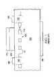
- FIG. 3illustrated is a cross sectional view of an embodiment of a semiconductor device (e.g. substrate driven FET) according to the principles of the present invention.
- the substrate driven FETis formed on a conductive substrate (e.g., GaAs substrate) 305 .
- the substrate 305may be chosen to be sufficiently thick to provide mechanical and chemical support for semiconductor processing and handling, and may be supported by a further underlying medium.
- the substrate 305provides a source connection for the substrate driven FET, accommodating a low-resistance connection over a substantial portion of the lower surface thereof.
- the substrate 305is preferably n+ doped and a preferred n-type doping element for GaAs is silicon (“Si”), but selenium (“Se”), tellurium (“Te”) or other doping materials or combinations thereof may be employed within the broad scope of the present invention.
- the substrate driven FET described hereinis GaAs based, alternative semiconductor materials may be employed to form the substrate 305 such as a semiconductor material based on indium-phosphide (“InP”) as well as oppositely doped semiconductors with essential properties of related materials appropriately altered.
- the crystal axes of the substrate 305may be aligned with the principal axes of the FIG. 3 or may be tilted slightly such as two degrees to produce a smoother surface for further crystal growth.
- first buffer layere.g., an n+ epitaxial buffer layer
- n+ epitaxial buffer layere.g., an n+ epitaxial buffer layer
- a suitable n-type doping elementsuch as Si may be employed, but alternatively Se, Te or other n-type dopant or combination thereof may be employed in the epitaxial growth process.
- the addition of the first buffer layer 310generally provides a more uniform crystal structure for further epitaxial depositions than an ordinary, doped GaAs substrate 305 , and thus may be optionally included in the formation of the substrate driven FET for improved device characteristics.
- the first buffer layer 310is an isolation layer (e.g., a p-doped isolation layer) 315 that is epitaxially grown and formed sufficiently thin to avoid leakage between a drain contact and the substrate 305 .
- the isolation layer 315is preferably connected to the source potential. Connecting the isolation layer 315 to a source will allow any charge buildup in the p-doped isolation layer to leak off, substantially avoiding any change in potential of the isolation layer 315 .
- Electrical connection to a source contactmay be obtained along the interface for the first buffer and isolation layers 310 , 315 (via tunneling or a leaky junction) or it may be engineering in the region of the metallization, if the metal makes a quasi-ohmic contact to the isolation layer 315 .
- the isolation layer 315therefore, is oppositely doped from or is a layer having an opposite carrier type from the substrate 305 and provides substantial electrical isolation between the substrate 305 and a lateral channel thereabove.
- a second buffer layer 320which may be provided to enhance the performance of the substrate driven FET, such as sustaining a high drain-to-source voltage (e.g., 20 volts) when the substrate driven FET is in a non-conducting state.
- the second buffer layer 320which may be undoped, also provides support for a lateral channel formed thereover.
- the second buffer layer 320is a lateral channel 325 that is epitaxially deposited to form a lateral channel with controllable conductivity.
- the lateral channel 325may be inherently lattice-strained (ie., it is “pseudomorphic”) and is preferably formed thin enough to prevent lattice dislocations and formation of polycrystalline structure in the layer(s) to be deposited thereabove.
- the lateral channel 325may provide higher carrier mobility owing to a reduced effective mass of the carriers.
- the lateral channel 325provides the controllable conduction mechanism between the source and drain contacts of the substrate driven FET.
- a barrier region 330that is preferably epitaxially deposited with aluminum-gallium arsenide (AlGaAs) to provide additional free carriers (electrons) for modulation doping of the lateral channel 325 , and to provide a barrier for the free carriers in the lateral channel 325 .
- a gatee.g., a plurality of gate fingers and one of which is designated 335 ) is formed over the barrier region 330 , wherein the gate is used to control the conductivity of lateral channel 325 , thereby controlling current conduction between the source and drain contacts of the substrate driven FET.
- a source via(e.g., a source trench 340 ) is etched through the barrier region 330 , lateral channel 325 , isolation layer 315 , and the first and second buffer layers 310 , 320 to the substrate 305 to form a source interconnect within the substrate driven FET.
- the walls of the source trenchmay be sufficiently sloped so that a thin metal layer (generally designated 345 ) can be deposited on horizontal and semi-horizontal surfaces, preferably by a vacuum evaporation and deposition process.
- the metallized sidewalls 345 of the source trench 340are designed to further enhance ohmic contacts for the source interconnect to connect the source trench 340 to the lateral channel 325 and the substrate 305 , thereby providing a low resistance connection between the source (embodied in the lateral channel 325 ) and the substrate 305 .
- Drain posts or fingers 350 of the FETare thereafter formed above the barrier region 330 to extend a connection for the drain (embodied in the lateral channel 325 ) to a top surface of the substrate driven FET.
- a dielectric layer 360may then be formed about the substrate driven FET, preferably with a low dielectric constant material (e.g. BCB, polyimide, Si glass, or other flowable oxide) to preserve a performance of the substrate driven FET.
- the dielectric layer 360is typically spun on and cured as necessary for planarization and for further surface passivation. The thickness of the dielectric layer 360 can be controlled by a spinning speed and duration. The cured dielectric layer 360 is strong enough to provide mechanical and chemical support for subsequent processing steps.
- Metallized top and bottom contacts(also referred to as drain and source contacts 370 , 380 , respectively) coupled to the drain post 350 and substrate 305 , respectively, are sequentially deposited and preferably patterned on the top and bottom surfaces, respectively, of the substrate driven FET.
- the drain contact 370interconnects the drain posts 350 , and may preferably occupy most of the surface area, since there may be little or no source metal that might interfere with the drain interconnects.
- the drain post 350can possibly be used to bond the drain to the package directly over the device itself, to further save area by eliminating the need for bond pads.
- the source contact 380is on a bottom surface of the substrate 305 .
- FIG. 4illustrated is a cross sectional view of an embodiment of a semiconductor device (e.g. substrate driven FET) according to the principles of the present invention.
- the structure of the substrate driven FET illustrated in FIG. 4is substantially similar to the substrate driven FET illustrated in FIG. 3 , with the exception of implant regions (e.g., n+ doped implant regions) 450 form a source interconnect within the substrate driven FET.
- the implant regions 450provide connection between a lateral channel 425 and a substrate 405 , thereby providing a low resistance connection between a source contact and the lateral channel 425 .
- the implant regions 450may be used in place of the source via 340 illustrated and described with respect to FIG. 3 , perhaps as a process simplification or a cost reduction, among other advantages, to form the source interconnect.
- FIG. 5illustrated is a plan view of another embodiment of a semiconductor device (e.g., substrate driven FET) constructed according to the principles of the present invention.
- a drain contact 510 of the substrate driven FETprovides a wide area surface covering a substantial portion of the die area, enabling a low-resistance contact to the drain.
- a gate contact 520 with gate extensions 530contacts a gate of the substrate driven FET.
- the couplings (not shown) between the gate extensions 530 on a top surface of the die and the gatemay be made by plated vias through a dielectric layer using well understood masking, patterning, etching and deposition processes.
- a metallized source contact(not shown) preferably covers substantially an entire area of the opposing die surface.
- FIG. 6illustrated is a plan view of another embodiment of a semiconductor device (e.g., substrate driven FET) constructed according to the principles of the present invention.
- a plurality of drain contacts 610 of the substrate driven FETprovide multiple drain contacts covering a substantial portion of the die area, enabling a low-resistance contact to the drain.
- a gate contact 620 with gate extensions 630contacts a gate of the substrate driven FET.
- the couplings (not shown) between the gate extensions 630 on a top surface of the die and the gatemay be made by plated vias through a dielectric layer using well understood masking, patterning, etching and deposition processes.
- drain contactFor a more detailed explanation of an embodiment of the drain contact, gate, and dielectric layer, see the description of the substrate driven FET as provided with respect to FIG. 3 , et seq.
- wire bond wires, solder bumps, or alternative connection techniquesmay be employed to interconnect the drain contacts 610 to a package or an electronic circuit board, for example.
- a metallized source contact(not shown) preferably covers substantially an entire area of the opposing die surface.
- an III-V field-effect transistorsuch as a GaAs— or InP-based metal extrinsic semiconductor field-effect transistor (MESFET), high electron mobility transistor (HEMT) or pseudomorphic high electron mobility transistor (pHEMT)
- MESFETmetal extrinsic semiconductor field-effect transistor
- HEMThigh electron mobility transistor
- pHEMTpseudomorphic high electron mobility transistor
- III-V field-effect transistorsuch as a GaAs— or InP-based metal extrinsic semiconductor field-effect transistor (MESFET), high electron mobility transistor (HEMT) or pseudomorphic high electron mobility transistor (pHEMT)
- MESFETmetal extrinsic semiconductor field-effect transistor
- HEMThigh electron mobility transistor
- pHEMTpseudomorphic high electron mobility transistor
- the structuremay preferably make use of a p-type region separating the n-substrate from the FET channel and drain, to reduce leakage currents.
- the structurecan also make use of bonding for the drain connection directly to the region on top of the devices, thereby possibly eliminating the need for a separate pad area.
- the resulting substrate driven FETcan be designed and packaged to exhibit very low on-resistance and be operable with very fast switching speeds.
- the substrateis typically semi-insulating, and there is a layer of metallization on the wafer surface to connect to the source regions.
- the FETs used to carry substantial amounts of current, such as devices for power switching and for power amplifiers, at presenthave many fingers, with a gate-to-gate spacing typically of 10-12 microns. With the proposed structure, smaller gate-to-gate spacing may be achieved, potentially down to 5 microns. The reduced spacing may permit a substantial reduction in the die area.
- the structurecan be used for high current/high power applications of FETs, particularly at frequencies below 10 GHz.
- the structureis well suited to switches for power converters. It is also potentially useful for transistors employed in microwave power amplifiers. These structures typically require very large equivalent gate widths, and thus require many fingers to be interconnected.
- the present inventionmay potentially make the devices less expensive to manufacture, owing to a reduced die size.
- the terms “above,” “formed over” or other similar terminology employed in reference to the semiconductor device or method of forming the sameshall not be limited to “directly above” or “directly formed over” and, unless otherwise specified, the scope of the present invention contemplates that intervening layers may be present when characterizing a layer above, over, formed over, etc. another layer.
Landscapes
- Junction Field-Effect Transistors (AREA)
Abstract
Description
Claims (20)
Priority Applications (1)
| Application Number | Priority Date | Filing Date | Title |
|---|---|---|---|
| US11/093,592US7439556B2 (en) | 2005-03-29 | 2005-03-29 | Substrate driven field-effect transistor |
Applications Claiming Priority (1)
| Application Number | Priority Date | Filing Date | Title |
|---|---|---|---|
| US11/093,592US7439556B2 (en) | 2005-03-29 | 2005-03-29 | Substrate driven field-effect transistor |
Publications (2)
| Publication Number | Publication Date |
|---|---|
| US20060226477A1 US20060226477A1 (en) | 2006-10-12 |
| US7439556B2true US7439556B2 (en) | 2008-10-21 |
Family
ID=37082389
Family Applications (1)
| Application Number | Title | Priority Date | Filing Date |
|---|---|---|---|
| US11/093,592Expired - LifetimeUS7439556B2 (en) | 2005-03-29 | 2005-03-29 | Substrate driven field-effect transistor |
Country Status (1)
| Country | Link |
|---|---|
| US (1) | US7439556B2 (en) |
Cited By (25)
| Publication number | Priority date | Publication date | Assignee | Title |
|---|---|---|---|---|
| US20070187717A1 (en)* | 2005-05-13 | 2007-08-16 | Coldwatt, Inc. | Semiconductor device having reduced on-resistance and method of forming the same |
| US20070298564A1 (en)* | 2006-06-21 | 2007-12-27 | Brar Berinder P S | Vertical Field-Effect Transistor and Method of Forming the Same |
| US20070298559A1 (en)* | 2006-06-21 | 2007-12-27 | Brar Berinder P S | Vertical Field-Effect Transistor and Method of Forming the Same |
| US20080048219A1 (en)* | 2005-08-25 | 2008-02-28 | Brar Berinder P S | Semiconductor Device Having Substrate-Driven Field-Effect Transistor and Schottky Diode and Method of Forming the Same |
| US20080157060A1 (en)* | 2005-05-13 | 2008-07-03 | Brar Berinder P S | Semiconductor Device Having Multiple Lateral Channels and Method of Forming the Same |
| US8520414B2 (en) | 2009-01-19 | 2013-08-27 | Power Systems Technologies, Ltd. | Controller for a power converter |
| US8638578B2 (en) | 2009-08-14 | 2014-01-28 | Power System Technologies, Ltd. | Power converter including a charge pump employable in a power adapter |
| US8643222B2 (en) | 2009-06-17 | 2014-02-04 | Power Systems Technologies Ltd | Power adapter employing a power reducer |
| US8767418B2 (en) | 2010-03-17 | 2014-07-01 | Power Systems Technologies Ltd. | Control system for a power converter and method of operating the same |
| US8787043B2 (en) | 2010-01-22 | 2014-07-22 | Power Systems Technologies, Ltd. | Controller for a power converter and method of operating the same |
| US8792257B2 (en) | 2011-03-25 | 2014-07-29 | Power Systems Technologies, Ltd. | Power converter with reduced power dissipation |
| US8792256B2 (en) | 2012-01-27 | 2014-07-29 | Power Systems Technologies Ltd. | Controller for a switch and method of operating the same |
| US8976549B2 (en) | 2009-12-03 | 2015-03-10 | Power Systems Technologies, Ltd. | Startup circuit including first and second Schmitt triggers and power converter employing the same |
| US9019061B2 (en) | 2009-03-31 | 2015-04-28 | Power Systems Technologies, Ltd. | Magnetic device formed with U-shaped core pieces and power converter employing the same |
| US9077248B2 (en) | 2009-06-17 | 2015-07-07 | Power Systems Technologies Ltd | Start-up circuit for a power adapter |
| US9088216B2 (en) | 2009-01-19 | 2015-07-21 | Power Systems Technologies, Ltd. | Controller for a synchronous rectifier switch |
| US9099232B2 (en) | 2012-07-16 | 2015-08-04 | Power Systems Technologies Ltd. | Magnetic device and power converter employing the same |
| US9106130B2 (en) | 2012-07-16 | 2015-08-11 | Power Systems Technologies, Inc. | Magnetic device and power converter employing the same |
| US9190898B2 (en) | 2012-07-06 | 2015-11-17 | Power Systems Technologies, Ltd | Controller for a power converter and method of operating the same |
| US9197132B2 (en) | 2006-12-01 | 2015-11-24 | Flextronics International Usa, Inc. | Power converter with an adaptive controller and method of operating the same |
| US9214264B2 (en) | 2012-07-16 | 2015-12-15 | Power Systems Technologies, Ltd. | Magnetic device and power converter employing the same |
| US9240712B2 (en) | 2012-12-13 | 2016-01-19 | Power Systems Technologies Ltd. | Controller including a common current-sense device for power switches of a power converter |
| US9246391B2 (en) | 2010-01-22 | 2016-01-26 | Power Systems Technologies Ltd. | Controller for providing a corrected signal to a sensed peak current through a circuit element of a power converter |
| US9300206B2 (en) | 2013-11-15 | 2016-03-29 | Power Systems Technologies Ltd. | Method for estimating power of a power converter |
| US9379629B2 (en) | 2012-07-16 | 2016-06-28 | Power Systems Technologies, Ltd. | Magnetic device and power converter employing the same |
Families Citing this family (24)
| Publication number | Priority date | Publication date | Assignee | Title |
|---|---|---|---|---|
| US7280026B2 (en) | 2002-04-18 | 2007-10-09 | Coldwatt, Inc. | Extended E matrix integrated magnetics (MIM) core |
| US7427910B2 (en) | 2004-08-19 | 2008-09-23 | Coldwatt, Inc. | Winding structure for efficient switch-mode power converters |
| US7321283B2 (en) | 2004-08-19 | 2008-01-22 | Coldwatt, Inc. | Vertical winding structures for planar magnetic switched-mode power converters |
| US7417875B2 (en) | 2005-02-08 | 2008-08-26 | Coldwatt, Inc. | Power converter employing integrated magnetics with a current multiplier rectifier and method of operating the same |
| US7176662B2 (en) | 2005-02-23 | 2007-02-13 | Coldwatt, Inc. | Power converter employing a tapped inductor and integrated magnetics and method of operating the same |
| US7876191B2 (en) | 2005-02-23 | 2011-01-25 | Flextronics International Usa, Inc. | Power converter employing a tapped inductor and integrated magnetics and method of operating the same |
| US7385375B2 (en) | 2005-02-23 | 2008-06-10 | Coldwatt, Inc. | Control circuit for a depletion mode switch and method of operating the same |
| US7439557B2 (en)* | 2005-03-29 | 2008-10-21 | Coldwatt, Inc. | Semiconductor device having a lateral channel and contacts on opposing surfaces thereof |
| US7564074B2 (en)* | 2005-08-25 | 2009-07-21 | Flextronics International Usa, Inc. | Semiconductor device including a lateral field-effect transistor and Schottky diode |
| US7462891B2 (en)* | 2005-09-27 | 2008-12-09 | Coldwatt, Inc. | Semiconductor device having an interconnect with sloped walls and method of forming the same |
| JP2007142144A (en)* | 2005-11-18 | 2007-06-07 | Matsushita Electric Ind Co Ltd | Field effect transistor integrated circuit and manufacturing method thereof |
| US7541640B2 (en)* | 2006-06-21 | 2009-06-02 | Flextronics International Usa, Inc. | Vertical field-effect transistor and method of forming the same |
| US8125205B2 (en) | 2006-08-31 | 2012-02-28 | Flextronics International Usa, Inc. | Power converter employing regulators with a coupled inductor |
| US7675758B2 (en) | 2006-12-01 | 2010-03-09 | Flextronics International Usa, Inc. | Power converter with an adaptive controller and method of operating the same |
| US7889517B2 (en) | 2006-12-01 | 2011-02-15 | Flextronics International Usa, Inc. | Power system with power converters having an adaptive controller |
| US7675759B2 (en) | 2006-12-01 | 2010-03-09 | Flextronics International Usa, Inc. | Power system with power converters having an adaptive controller |
| US7667986B2 (en) | 2006-12-01 | 2010-02-23 | Flextronics International Usa, Inc. | Power system with power converters having an adaptive controller |
| US7468649B2 (en) | 2007-03-14 | 2008-12-23 | Flextronics International Usa, Inc. | Isolated power converter |
| US20080316779A1 (en) | 2007-06-19 | 2008-12-25 | Chandrasekaran Jayaraman | System and method for estimating input power for a power processing circuit |
| US7880284B2 (en)* | 2007-09-29 | 2011-02-01 | Intel Corporation | Embedded power gating |
| US8514593B2 (en) | 2009-06-17 | 2013-08-20 | Power Systems Technologies, Ltd. | Power converter employing a variable switching frequency and a magnetic device with a non-uniform gap |
| US8520420B2 (en) | 2009-12-18 | 2013-08-27 | Power Systems Technologies, Ltd. | Controller for modifying dead time between switches in a power converter |
| US8319256B2 (en) | 2010-06-23 | 2012-11-27 | Power Integrations, Inc. | Layout design for a high power, GaN-based FET |
| US10461172B2 (en) | 2017-12-21 | 2019-10-29 | International Business Machines Corporation | Vertical transistors having improved gate length control using uniformly deposited spacers |
Citations (66)
| Publication number | Priority date | Publication date | Assignee | Title |
|---|---|---|---|---|
| US4499481A (en) | 1983-09-14 | 1985-02-12 | The United States Of America As Represented By The Secretary Of The Navy | Heterojunction Schottky gate MESFET with lower channel ridge barrier |
| US4570174A (en) | 1981-08-21 | 1986-02-11 | The United States Of America As Represented By The Secretary Of The Army | Vertical MESFET with air spaced gate electrode |
| US4636823A (en) | 1984-06-05 | 1987-01-13 | California Institute Of Technology | Vertical Schottky barrier gate field-effect transistor in GaAs/GaAlAs |
| US4807022A (en) | 1987-05-01 | 1989-02-21 | Raytheon Company | Simultaneous formation of via hole and tub structures for GaAs monolithic microwave integrated circuits |
| US4903089A (en) | 1988-02-02 | 1990-02-20 | Massachusetts Institute Of Technology | Vertical transistor device fabricated with semiconductor regrowth |
| US4967243A (en) | 1988-07-19 | 1990-10-30 | General Electric Company | Power transistor structure with high speed integral antiparallel Schottky diode |
| US5068756A (en) | 1989-02-16 | 1991-11-26 | Texas Instruments Incorporated | Integrated circuit composed of group III-V compound field effect and bipolar semiconductors |
| US5106778A (en) | 1988-02-02 | 1992-04-21 | Massachusetts Institute Of Technology | Vertical transistor device fabricated with semiconductor regrowth |
| US5126701A (en)* | 1990-12-28 | 1992-06-30 | Raytheon Company | Avalanche diode limiters |
| US5126714A (en) | 1990-12-20 | 1992-06-30 | The United States Of America As Represented By The Secretary Of The Navy | Integrated circuit transformer |
| US5223449A (en) | 1989-02-16 | 1993-06-29 | Morris Francis J | Method of making an integrated circuit composed of group III-V compound field effect and bipolar semiconductors |
| US5231037A (en) | 1992-04-30 | 1993-07-27 | Texas Instruments Incorporated | Method of making a power VFET device using a p+ carbon doped gate layer |
| US5244829A (en) | 1992-07-09 | 1993-09-14 | Texas Instruments Incorporated | Organometallic vapor-phase epitaxy process using (CH3)3 As and CCl4 for improving stability of carbon-doped GaAs |
| US5292686A (en)* | 1991-08-21 | 1994-03-08 | Triquint Semiconductor, Inc. | Method of forming substrate vias in a GaAs wafer |
| US5343071A (en)* | 1993-04-28 | 1994-08-30 | Raytheon Company | Semiconductor structures having dual surface via holes |
| US5342795A (en) | 1992-04-30 | 1994-08-30 | Texas Instruments Incorporated | Method of fabricating power VFET gate-refill |
| US5369042A (en) | 1993-03-05 | 1994-11-29 | Texas Instruments Incorporated | Enhanced performance bipolar transistor process |
| US5374887A (en) | 1993-11-12 | 1994-12-20 | Northern Telecom Limited | Inrush current limiting circuit |
| US5468661A (en) | 1993-06-17 | 1995-11-21 | Texas Instruments Incorporated | Method of making power VFET device |
| US5554561A (en) | 1993-04-30 | 1996-09-10 | Texas Instruments Incorporated | Epitaxial overgrowth method |
| US5555494A (en) | 1993-09-13 | 1996-09-10 | Morris; George Q. | Magnetically integrated full wave DC to DC converter |
| US5610085A (en) | 1993-11-29 | 1997-03-11 | Texas Instruments Incorporated | Method of making a vertical FET using epitaxial overgrowth |
| US5624860A (en) | 1993-04-30 | 1997-04-29 | Texas Instruments Incorporated | Vertical field effect transistor and method |
| US5700703A (en) | 1996-08-06 | 1997-12-23 | Motorola | Method of fabricating buried control elements in semiconductor devices |
| US5712189A (en) | 1993-04-30 | 1998-01-27 | Texas Instruments Incorporated | Epitaxial overgrowth method |
| US5756375A (en) | 1995-06-14 | 1998-05-26 | Texas Instruments Incorporated | Semiconductor growth method with thickness control |
| US5783984A (en) | 1995-06-16 | 1998-07-21 | Hughes Electronics | Method and means for combining a transformer and inductor on a single core structure |
| US5784266A (en) | 1996-06-14 | 1998-07-21 | Virginia Power Technologies, Inc | Single magnetic low loss high frequency converter |
| US5804943A (en) | 1995-05-12 | 1998-09-08 | Texas Instruments Incorporated | Resonant bilateral charging and discharging circuit |
| US5909110A (en) | 1996-12-17 | 1999-06-01 | Texas Insturments Incorporated | Integrated voltage regulator circuit with vertical transistor |
| US5910665A (en) | 1995-12-29 | 1999-06-08 | Texas Instruments Incorporated | Low capacitance power VFET method and device |
| US5920475A (en) | 1995-05-04 | 1999-07-06 | Lucent Technologies Inc. | Circuit and method for controlling a synchronous rectifier converter |
| US5956578A (en) | 1997-04-23 | 1999-09-21 | Motorola, Inc. | Method of fabricating vertical FET with Schottky diode |
| US6008519A (en) | 1996-12-16 | 1999-12-28 | Texas Instruments Incorporated | Vertical transistor and method |
| US6094038A (en) | 1999-06-28 | 2000-07-25 | Semtech Corporation | Buck converter with inductive turn ratio optimization |
| US6097046A (en) | 1993-04-30 | 2000-08-01 | Texas Instruments Incorporated | Vertical field effect transistor and diode |
| US6156611A (en) | 1998-07-20 | 2000-12-05 | Motorola, Inc. | Method of fabricating vertical FET with sidewall gate electrode |
| US6181231B1 (en) | 1998-04-06 | 2001-01-30 | Silicon Graphics, Inc. | Diamond-based transformers and power convertors |
| US6208535B1 (en) | 1994-10-31 | 2001-03-27 | Texas Instruments Incorporated | Resonant gate driver |
| US6218891B1 (en) | 2000-07-28 | 2001-04-17 | Lucent Technologies Inc. | Integrated circuit including a driver for a metal-semiconductor field-effect transistor |
| US6229197B1 (en) | 1993-04-30 | 2001-05-08 | Texas Instruments Incorporated | Epitaxial overgrowth method and devices |
| US6309918B1 (en) | 1998-09-21 | 2001-10-30 | Motorola, Inc. | Manufacturable GaAs VFET process |
| US6323090B1 (en) | 1999-06-09 | 2001-11-27 | Ixys Corporation | Semiconductor device with trenched substrate and method |
| US6348848B1 (en) | 2000-05-04 | 2002-02-19 | Edward Herbert | Transformer having fractional turn windings |
| US6362986B1 (en) | 2001-03-22 | 2002-03-26 | Volterra, Inc. | Voltage converter with coupled inductive windings, and associated methods |
| US20020121647A1 (en) | 2001-03-02 | 2002-09-05 | Taylor Geoff W. | Modulation doped thyristor and complementary transistor combination for a monolithic optoelectronic integrated circuit |
| EP1256985A2 (en) | 2001-05-09 | 2002-11-13 | Kabushiki Kaisha Toshiba | Lateral power MISFET |
| US6483724B1 (en) | 2002-02-15 | 2002-11-19 | Valere Power, Inc. | DC/DC ZVS full bridge converter power supply method and apparatus |
| US6525603B1 (en) | 2001-01-05 | 2003-02-25 | Remec, Inc. | Feedforward amplifier linearization adapting off modulation |
| US6549436B1 (en) | 2002-02-21 | 2003-04-15 | Innovative Technology Licensing Llc | Integrated magnetic converter circuit and method with improved filtering |
| US20030198067A1 (en) | 2002-04-18 | 2003-10-23 | Innovative Technology Licensing, Llc | Core structure and interleaved DC-DC converter topology |
| US6661276B1 (en) | 2002-07-29 | 2003-12-09 | Lovoltech Inc. | MOSFET driver matching circuit for an enhancement mode JFET |
| US6741099B1 (en) | 2003-01-31 | 2004-05-25 | Power-One Limited | Transistor driver circuit |
| US6775159B2 (en) | 2001-02-19 | 2004-08-10 | Rockwell Scientific Company, Llc. | Switching power converter circuits providing main and auxiliary output voltages |
| US20050024179A1 (en) | 2002-04-18 | 2005-02-03 | Rockwell Scientific Licensing, Llc | Extended E matrix integrated magnetics (MIM) core |
| WO2005015642A1 (en)* | 2003-08-08 | 2005-02-17 | Sanken Electric Co., Ltd. | Semiconductor device and manufacturing method thereof |
| US6873237B2 (en) | 2002-04-18 | 2005-03-29 | Innovative Technology Licensing, Llc | Core structure |
| US20050104080A1 (en)* | 2003-11-19 | 2005-05-19 | Takashi Ichihara | Semiconductor element and manufacturing method for the same |
| US6980077B1 (en) | 2004-08-19 | 2005-12-27 | Coldwatt, Inc. | Composite magnetic core for switch-mode power converters |
| US20060038650A1 (en) | 2004-08-19 | 2006-02-23 | Rockwell Scientific Licensing, Llc | Vertical winding structures for planar magnetic switched-mode power converters |
| US7012414B1 (en) | 2004-08-19 | 2006-03-14 | Coldwatt, Inc. | Vertically packaged switched-mode power converter |
| EP1638147A2 (en) | 2004-09-17 | 2006-03-22 | Matsushita Electric Industrial Co., Ltd. | III-V nitride semiconductor device and method for fabricating the same |
| US20060187684A1 (en) | 2005-02-08 | 2006-08-24 | Sriram Chandrasekaran | Power converter employing integrated magnetics with a current multiplier rectifier and method of operating the same |
| US20060197510A1 (en) | 2005-02-23 | 2006-09-07 | Sriram Chandrasekaran | Power converter employing a tapped inductor and integrated magnetics and method of operating the same |
| US20060198173A1 (en) | 2005-02-23 | 2006-09-07 | Rozman Allen F | Control circuit for a depletion mode switch and method of operating the same |
| US20060208279A1 (en) | 2005-03-15 | 2006-09-21 | Robinson Kevin L | Multi-layer structure for use in the fabrication of integrated circuit devices and methods for fabrication of same |
Family Cites Families (1)
| Publication number | Priority date | Publication date | Assignee | Title |
|---|---|---|---|---|
| US6309916B1 (en)* | 1999-11-17 | 2001-10-30 | Amkor Technology, Inc | Method of molding plastic semiconductor packages |
- 2005
- 2005-03-29USUS11/093,592patent/US7439556B2/ennot_activeExpired - Lifetime
Patent Citations (77)
| Publication number | Priority date | Publication date | Assignee | Title |
|---|---|---|---|---|
| US4570174A (en) | 1981-08-21 | 1986-02-11 | The United States Of America As Represented By The Secretary Of The Army | Vertical MESFET with air spaced gate electrode |
| US4499481A (en) | 1983-09-14 | 1985-02-12 | The United States Of America As Represented By The Secretary Of The Navy | Heterojunction Schottky gate MESFET with lower channel ridge barrier |
| US4636823A (en) | 1984-06-05 | 1987-01-13 | California Institute Of Technology | Vertical Schottky barrier gate field-effect transistor in GaAs/GaAlAs |
| US4807022A (en) | 1987-05-01 | 1989-02-21 | Raytheon Company | Simultaneous formation of via hole and tub structures for GaAs monolithic microwave integrated circuits |
| US4903089A (en) | 1988-02-02 | 1990-02-20 | Massachusetts Institute Of Technology | Vertical transistor device fabricated with semiconductor regrowth |
| US5106778A (en) | 1988-02-02 | 1992-04-21 | Massachusetts Institute Of Technology | Vertical transistor device fabricated with semiconductor regrowth |
| US4967243A (en) | 1988-07-19 | 1990-10-30 | General Electric Company | Power transistor structure with high speed integral antiparallel Schottky diode |
| US5223449A (en) | 1989-02-16 | 1993-06-29 | Morris Francis J | Method of making an integrated circuit composed of group III-V compound field effect and bipolar semiconductors |
| US5068756A (en) | 1989-02-16 | 1991-11-26 | Texas Instruments Incorporated | Integrated circuit composed of group III-V compound field effect and bipolar semiconductors |
| US5126714A (en) | 1990-12-20 | 1992-06-30 | The United States Of America As Represented By The Secretary Of The Navy | Integrated circuit transformer |
| US5126701A (en)* | 1990-12-28 | 1992-06-30 | Raytheon Company | Avalanche diode limiters |
| US5292686A (en)* | 1991-08-21 | 1994-03-08 | Triquint Semiconductor, Inc. | Method of forming substrate vias in a GaAs wafer |
| US5231037A (en) | 1992-04-30 | 1993-07-27 | Texas Instruments Incorporated | Method of making a power VFET device using a p+ carbon doped gate layer |
| US5342795A (en) | 1992-04-30 | 1994-08-30 | Texas Instruments Incorporated | Method of fabricating power VFET gate-refill |
| US5244829A (en) | 1992-07-09 | 1993-09-14 | Texas Instruments Incorporated | Organometallic vapor-phase epitaxy process using (CH3)3 As and CCl4 for improving stability of carbon-doped GaAs |
| US5369042A (en) | 1993-03-05 | 1994-11-29 | Texas Instruments Incorporated | Enhanced performance bipolar transistor process |
| US5407842A (en) | 1993-03-05 | 1995-04-18 | Texas Intruments Incorporated | Enhanced performance bipolar transistor process |
| US5343071A (en)* | 1993-04-28 | 1994-08-30 | Raytheon Company | Semiconductor structures having dual surface via holes |
| US5554561A (en) | 1993-04-30 | 1996-09-10 | Texas Instruments Incorporated | Epitaxial overgrowth method |
| US5712189A (en) | 1993-04-30 | 1998-01-27 | Texas Instruments Incorporated | Epitaxial overgrowth method |
| US6229197B1 (en) | 1993-04-30 | 2001-05-08 | Texas Instruments Incorporated | Epitaxial overgrowth method and devices |
| US5889298A (en) | 1993-04-30 | 1999-03-30 | Texas Instruments Incorporated | Vertical JFET field effect transistor |
| US5747842A (en) | 1993-04-30 | 1998-05-05 | Texas Instruments Incorporated | Epitaxial overgrowth method and devices |
| US5624860A (en) | 1993-04-30 | 1997-04-29 | Texas Instruments Incorporated | Vertical field effect transistor and method |
| US6097046A (en) | 1993-04-30 | 2000-08-01 | Texas Instruments Incorporated | Vertical field effect transistor and diode |
| US5468661A (en) | 1993-06-17 | 1995-11-21 | Texas Instruments Incorporated | Method of making power VFET device |
| US5555494A (en) | 1993-09-13 | 1996-09-10 | Morris; George Q. | Magnetically integrated full wave DC to DC converter |
| US5374887A (en) | 1993-11-12 | 1994-12-20 | Northern Telecom Limited | Inrush current limiting circuit |
| US5610085A (en) | 1993-11-29 | 1997-03-11 | Texas Instruments Incorporated | Method of making a vertical FET using epitaxial overgrowth |
| US6477065B2 (en) | 1994-10-31 | 2002-11-05 | Texas Instruments Incorporated | Resonant gate driver |
| US6208535B1 (en) | 1994-10-31 | 2001-03-27 | Texas Instruments Incorporated | Resonant gate driver |
| US5920475A (en) | 1995-05-04 | 1999-07-06 | Lucent Technologies Inc. | Circuit and method for controlling a synchronous rectifier converter |
| US5956245A (en) | 1995-05-04 | 1999-09-21 | Lucent Technologies Inc. | Circuit and method for controlling a synchronous rectifier converter |
| US6191964B1 (en) | 1995-05-04 | 2001-02-20 | Lucent Technologies Inc. | Circuit and method for controlling a synchronous rectifier converter |
| US6038154A (en) | 1995-05-04 | 2000-03-14 | Lucent Technologies Inc. | Circuit and method for controlling a synchronous rectifier converter |
| US5804943A (en) | 1995-05-12 | 1998-09-08 | Texas Instruments Incorporated | Resonant bilateral charging and discharging circuit |
| US5756375A (en) | 1995-06-14 | 1998-05-26 | Texas Instruments Incorporated | Semiconductor growth method with thickness control |
| US5783984A (en) | 1995-06-16 | 1998-07-21 | Hughes Electronics | Method and means for combining a transformer and inductor on a single core structure |
| US5910665A (en) | 1995-12-29 | 1999-06-08 | Texas Instruments Incorporated | Low capacitance power VFET method and device |
| US5784266A (en) | 1996-06-14 | 1998-07-21 | Virginia Power Technologies, Inc | Single magnetic low loss high frequency converter |
| US5700703A (en) | 1996-08-06 | 1997-12-23 | Motorola | Method of fabricating buried control elements in semiconductor devices |
| US6008519A (en) | 1996-12-16 | 1999-12-28 | Texas Instruments Incorporated | Vertical transistor and method |
| US5909110A (en) | 1996-12-17 | 1999-06-01 | Texas Insturments Incorporated | Integrated voltage regulator circuit with vertical transistor |
| US5956578A (en) | 1997-04-23 | 1999-09-21 | Motorola, Inc. | Method of fabricating vertical FET with Schottky diode |
| US6181231B1 (en) | 1998-04-06 | 2001-01-30 | Silicon Graphics, Inc. | Diamond-based transformers and power convertors |
| US6156611A (en) | 1998-07-20 | 2000-12-05 | Motorola, Inc. | Method of fabricating vertical FET with sidewall gate electrode |
| US6309918B1 (en) | 1998-09-21 | 2001-10-30 | Motorola, Inc. | Manufacturable GaAs VFET process |
| US6323090B1 (en) | 1999-06-09 | 2001-11-27 | Ixys Corporation | Semiconductor device with trenched substrate and method |
| US6094038A (en) | 1999-06-28 | 2000-07-25 | Semtech Corporation | Buck converter with inductive turn ratio optimization |
| US6348848B1 (en) | 2000-05-04 | 2002-02-19 | Edward Herbert | Transformer having fractional turn windings |
| US6218891B1 (en) | 2000-07-28 | 2001-04-17 | Lucent Technologies Inc. | Integrated circuit including a driver for a metal-semiconductor field-effect transistor |
| US6525603B1 (en) | 2001-01-05 | 2003-02-25 | Remec, Inc. | Feedforward amplifier linearization adapting off modulation |
| US6775159B2 (en) | 2001-02-19 | 2004-08-10 | Rockwell Scientific Company, Llc. | Switching power converter circuits providing main and auxiliary output voltages |
| US20020121647A1 (en) | 2001-03-02 | 2002-09-05 | Taylor Geoff W. | Modulation doped thyristor and complementary transistor combination for a monolithic optoelectronic integrated circuit |
| US6362986B1 (en) | 2001-03-22 | 2002-03-26 | Volterra, Inc. | Voltage converter with coupled inductive windings, and associated methods |
| EP1256985A2 (en) | 2001-05-09 | 2002-11-13 | Kabushiki Kaisha Toshiba | Lateral power MISFET |
| US6483724B1 (en) | 2002-02-15 | 2002-11-19 | Valere Power, Inc. | DC/DC ZVS full bridge converter power supply method and apparatus |
| US6549436B1 (en) | 2002-02-21 | 2003-04-15 | Innovative Technology Licensing Llc | Integrated magnetic converter circuit and method with improved filtering |
| US20030198067A1 (en) | 2002-04-18 | 2003-10-23 | Innovative Technology Licensing, Llc | Core structure and interleaved DC-DC converter topology |
| US7046523B2 (en) | 2002-04-18 | 2006-05-16 | Coldwatt, Inc. | Core structure and interleaved DC—DC converter topology |
| US6873237B2 (en) | 2002-04-18 | 2005-03-29 | Innovative Technology Licensing, Llc | Core structure |
| US20050024179A1 (en) | 2002-04-18 | 2005-02-03 | Rockwell Scientific Licensing, Llc | Extended E matrix integrated magnetics (MIM) core |
| US6661276B1 (en) | 2002-07-29 | 2003-12-09 | Lovoltech Inc. | MOSFET driver matching circuit for an enhancement mode JFET |
| US6741099B1 (en) | 2003-01-31 | 2004-05-25 | Power-One Limited | Transistor driver circuit |
| US20060118824A1 (en) | 2003-08-08 | 2006-06-08 | Sanken Electric Co., Ltd. | Semiconductor device with reduced leakage current, and method of fabrication |
| WO2005015642A1 (en)* | 2003-08-08 | 2005-02-17 | Sanken Electric Co., Ltd. | Semiconductor device and manufacturing method thereof |
| US20050104080A1 (en)* | 2003-11-19 | 2005-05-19 | Takashi Ichihara | Semiconductor element and manufacturing method for the same |
| US20060038650A1 (en) | 2004-08-19 | 2006-02-23 | Rockwell Scientific Licensing, Llc | Vertical winding structures for planar magnetic switched-mode power converters |
| US7012414B1 (en) | 2004-08-19 | 2006-03-14 | Coldwatt, Inc. | Vertically packaged switched-mode power converter |
| US6980077B1 (en) | 2004-08-19 | 2005-12-27 | Coldwatt, Inc. | Composite magnetic core for switch-mode power converters |
| US7321283B2 (en) | 2004-08-19 | 2008-01-22 | Coldwatt, Inc. | Vertical winding structures for planar magnetic switched-mode power converters |
| EP1638147A2 (en) | 2004-09-17 | 2006-03-22 | Matsushita Electric Industrial Co., Ltd. | III-V nitride semiconductor device and method for fabricating the same |
| US20060187684A1 (en) | 2005-02-08 | 2006-08-24 | Sriram Chandrasekaran | Power converter employing integrated magnetics with a current multiplier rectifier and method of operating the same |
| US20060197510A1 (en) | 2005-02-23 | 2006-09-07 | Sriram Chandrasekaran | Power converter employing a tapped inductor and integrated magnetics and method of operating the same |
| US20060198173A1 (en) | 2005-02-23 | 2006-09-07 | Rozman Allen F | Control circuit for a depletion mode switch and method of operating the same |
| US7176662B2 (en) | 2005-02-23 | 2007-02-13 | Coldwatt, Inc. | Power converter employing a tapped inductor and integrated magnetics and method of operating the same |
| US20060208279A1 (en) | 2005-03-15 | 2006-09-21 | Robinson Kevin L | Multi-layer structure for use in the fabrication of integrated circuit devices and methods for fabrication of same |
Non-Patent Citations (19)
| Title |
|---|
| Ajit, J.S., "Design of MOS-Gated Bipolar Transistors with Integral Antiparallel Diode," IEEE Electron Device Letters, pp. 344-347, Jul. 1996, vol. 17, No. 7, IEEE, Los Alamitos, CA. |
| Asano, K., et al., "Novel High Power AlGaAs/GaAs HFET with a Field-Modulating Plate Operated at 35V Drain Voltage," IEDM 98, 1998, pp. 59-62, IEEE, Los Alamitos, CA. |
| Bergman, J., "Development of Indium Arsenide Quantum Well Electronic Circuits: A Dissertation Presented to the Academic Faculty," http://smartech.gatech.edu/bitstream/1853/5033/1/bergman<SUB>-</SUB>joshua<SUB>-</SUB>i<SUB>-</SUB>200407<SUB>-</SUB>phd.pdf, Jul. 2004, 225 pp., Georgia Institute of Technology, Atlanta, GA. |
| Berroth, M., et al., "Extreme Low Power 1:4 Demultiplexer Using Double Delta Doped Quantum Well GaAs/AlGaAs Transistors," Japanese Journal of Applied Physics, Extended Abstracts of the 22nd 1990 International Conference on Solid State Devices and Materials, 1990, pp. 75-78, Tokyo, Japan. |
| Eisenbeiser, K., et al., "Manufacturable GaAs VFET for Power Switching Applications," IEEE Electron Device Letters, Apr. 2000, pp. 144-145, vol. 21, No. 4, IEEE. |
| Kollman, R., et al., "10 MHz PWM Converters with GaAs VFETs," IEEE Eleventh Annual Applied Power Electronics Conference and Exposition, Mar. 1996, pp. 264-269, vol. 1, IEEE. |
| Lan, E., et al., "A Field Plate Device by Self-Aligned Spacer Process," The International Conference of Compound Semiconductor Manufacturing Technology, 2004, pp. 35-38, GaAs Mantech, St. Louis, MO. |
| Liu, W., "Fundamentals of III-V Devices: HBTs, MESFETs, and HFETs/HEMTs," §5-5: Modulation Doping, 1999, pp. 323-330, John Wiley & Sons, New York, NY. |
| Nguyen, L.D., et al., "Ultra-High-Speed Modulation-Doped Field-Effect Transistors: A Tutorial Review," Proceedings of the IEEE, Apr. 1992, pp. 494-518, vol. 80, No. 4, IEEE. |
| Niemela, V.A., et al., "Comparison of GaAs and Silicon Synchronous Rectifiers in a 3.3V Out, 50W DC-DC Converter," 27th Annual, IEEE Power Electronics Specialists Conference, Jun. 1996, pp. 861-867, vol. 1, IEEE. |
| Peppel, M., et al., "Optimized Reverse Diode Operation of Power MOSFETs," 2000 IEEE Industry Applications Conference, Oct. 8, 2000, pp. 2961-2965, vol. 5, IEEE, Los Alamitos, CA. |
| Plumton, D.L., et al., "A Low On-Resistance High-Current GaAs Power VFET," IEEE Electron Device Letters, Apr. 1995, pp. 142-144, vol. 16, No. 4, IEEE. |
| Sickmiller, M., "Packaging of Ultrathin Semiconductor Devices Through the ELO Packaging Process," Mat. Res. Soc. Symp. Proc., 2001, pp. 17.3.1-17.3.6, vol. 681E, Materials Research Society, Warrendale, PA. |
| Storm, D.F., et al., "Reduction of Buffer Layer Conduction Near Plasma-Assisted Molecular-Beam Epitaxy Grown GaN/AIN Interfaces by Beryllium Doping," Applied Physics Letters, Nov. 11, 2002, pp. 3819-3821, vol. 81, No. 20, American Institute of Physics, Melville, NY. |
| Tkachenko, Y., et al., "Improved Breakdown Voltage and Hot-Electron Reliability PHEMT for High Efficiency Power Amplifiers," Asia Pacific Microwave Conference (AMPC'99), Nov. 30, 1999, pp. 618-621, vol. 3, IEEE, Los Alamitos, CA. |
| U.S. Appl. No. 11/211,964, filed Aug. 25, 2005, Brar et al. |
| Weitzel, C.E., "RF Power Devices for Wireless Communications," 2002, 2002 IEEE MTT-S CDROM, paper TU4B-1, IEEE. |
| Williams, R., "Modern GaAs Processing Methods," 1990, pp. 66-67, Artech House, Inc., Norwood, MA. |
| Wu, C.S., et al., "Pseudomorphic HEMT Manufacturing Technology for Multifunctional Ka-Band MMIC Applications," IEEE Transactions on Microwave Theory and Techniques, Feb. 1995, pp. 257-265, vol. 43, No. 2, IEEE, New York, US. |
Cited By (32)
| Publication number | Priority date | Publication date | Assignee | Title |
|---|---|---|---|---|
| US7838905B2 (en) | 2005-05-13 | 2010-11-23 | Flextronics International Usa, Inc. | Semiconductor device having multiple lateral channels and method of forming the same |
| US7675090B2 (en) | 2005-05-13 | 2010-03-09 | Flextronics International Usa, Inc. | Semiconductor device having a contact on a buffer layer thereof and method of forming the same |
| US20070187717A1 (en)* | 2005-05-13 | 2007-08-16 | Coldwatt, Inc. | Semiconductor device having reduced on-resistance and method of forming the same |
| US20080157060A1 (en)* | 2005-05-13 | 2008-07-03 | Brar Berinder P S | Semiconductor Device Having Multiple Lateral Channels and Method of Forming the Same |
| US20080048219A1 (en)* | 2005-08-25 | 2008-02-28 | Brar Berinder P S | Semiconductor Device Having Substrate-Driven Field-Effect Transistor and Schottky Diode and Method of Forming the Same |
| US20080048174A1 (en)* | 2005-08-25 | 2008-02-28 | Sadaka Mariam G | Semiconductor Device Including a Lateral Field-Effect Transistor and Schottky Diode |
| US7642568B2 (en) | 2005-08-25 | 2010-01-05 | Flextronics International Usa, Inc. | Semiconductor device having substrate-driven field-effect transistor and Schottky diode and method of forming the same |
| US7655963B2 (en) | 2005-08-25 | 2010-02-02 | Flextronics International Usa, Inc. | Semiconductor device including a lateral field-effect transistor and Schottky diode |
| US20070298564A1 (en)* | 2006-06-21 | 2007-12-27 | Brar Berinder P S | Vertical Field-Effect Transistor and Method of Forming the Same |
| US7663183B2 (en) | 2006-06-21 | 2010-02-16 | Flextronics International Usa, Inc. | Vertical field-effect transistor and method of forming the same |
| US8415737B2 (en) | 2006-06-21 | 2013-04-09 | Flextronics International Usa, Inc. | Semiconductor device with a pillar region and method of forming the same |
| US20070298559A1 (en)* | 2006-06-21 | 2007-12-27 | Brar Berinder P S | Vertical Field-Effect Transistor and Method of Forming the Same |
| US9197132B2 (en) | 2006-12-01 | 2015-11-24 | Flextronics International Usa, Inc. | Power converter with an adaptive controller and method of operating the same |
| US8520414B2 (en) | 2009-01-19 | 2013-08-27 | Power Systems Technologies, Ltd. | Controller for a power converter |
| US9088216B2 (en) | 2009-01-19 | 2015-07-21 | Power Systems Technologies, Ltd. | Controller for a synchronous rectifier switch |
| US9019061B2 (en) | 2009-03-31 | 2015-04-28 | Power Systems Technologies, Ltd. | Magnetic device formed with U-shaped core pieces and power converter employing the same |
| US8643222B2 (en) | 2009-06-17 | 2014-02-04 | Power Systems Technologies Ltd | Power adapter employing a power reducer |
| US9077248B2 (en) | 2009-06-17 | 2015-07-07 | Power Systems Technologies Ltd | Start-up circuit for a power adapter |
| US8638578B2 (en) | 2009-08-14 | 2014-01-28 | Power System Technologies, Ltd. | Power converter including a charge pump employable in a power adapter |
| US8976549B2 (en) | 2009-12-03 | 2015-03-10 | Power Systems Technologies, Ltd. | Startup circuit including first and second Schmitt triggers and power converter employing the same |
| US8787043B2 (en) | 2010-01-22 | 2014-07-22 | Power Systems Technologies, Ltd. | Controller for a power converter and method of operating the same |
| US9246391B2 (en) | 2010-01-22 | 2016-01-26 | Power Systems Technologies Ltd. | Controller for providing a corrected signal to a sensed peak current through a circuit element of a power converter |
| US8767418B2 (en) | 2010-03-17 | 2014-07-01 | Power Systems Technologies Ltd. | Control system for a power converter and method of operating the same |
| US8792257B2 (en) | 2011-03-25 | 2014-07-29 | Power Systems Technologies, Ltd. | Power converter with reduced power dissipation |
| US8792256B2 (en) | 2012-01-27 | 2014-07-29 | Power Systems Technologies Ltd. | Controller for a switch and method of operating the same |
| US9190898B2 (en) | 2012-07-06 | 2015-11-17 | Power Systems Technologies, Ltd | Controller for a power converter and method of operating the same |
| US9099232B2 (en) | 2012-07-16 | 2015-08-04 | Power Systems Technologies Ltd. | Magnetic device and power converter employing the same |
| US9106130B2 (en) | 2012-07-16 | 2015-08-11 | Power Systems Technologies, Inc. | Magnetic device and power converter employing the same |
| US9214264B2 (en) | 2012-07-16 | 2015-12-15 | Power Systems Technologies, Ltd. | Magnetic device and power converter employing the same |
| US9379629B2 (en) | 2012-07-16 | 2016-06-28 | Power Systems Technologies, Ltd. | Magnetic device and power converter employing the same |
| US9240712B2 (en) | 2012-12-13 | 2016-01-19 | Power Systems Technologies Ltd. | Controller including a common current-sense device for power switches of a power converter |
| US9300206B2 (en) | 2013-11-15 | 2016-03-29 | Power Systems Technologies Ltd. | Method for estimating power of a power converter |
Also Published As
| Publication number | Publication date |
|---|---|
| US20060226477A1 (en) | 2006-10-12 |
Similar Documents
| Publication | Publication Date | Title |
|---|---|---|
| US7439556B2 (en) | Substrate driven field-effect transistor | |
| US7439557B2 (en) | Semiconductor device having a lateral channel and contacts on opposing surfaces thereof | |
| US7838905B2 (en) | Semiconductor device having multiple lateral channels and method of forming the same | |
| US7285807B2 (en) | Semiconductor device having substrate-driven field-effect transistor and Schottky diode and method of forming the same | |
| US7462891B2 (en) | Semiconductor device having an interconnect with sloped walls and method of forming the same | |
| US7675090B2 (en) | Semiconductor device having a contact on a buffer layer thereof and method of forming the same | |
| US11888027B2 (en) | Monolithic integration of high and low-side GaN FETs with screening back gating effect | |
| US8981380B2 (en) | Monolithic integration of silicon and group III-V devices | |
| US7564074B2 (en) | Semiconductor device including a lateral field-effect transistor and Schottky diode | |
| US9219058B2 (en) | Efficient high voltage switching circuits and monolithic integration of same | |
| US8415737B2 (en) | Semiconductor device with a pillar region and method of forming the same | |
| US7663183B2 (en) | Vertical field-effect transistor and method of forming the same | |
| US7541640B2 (en) | Vertical field-effect transistor and method of forming the same | |
| US9171937B2 (en) | Monolithically integrated vertical JFET and Schottky diode |
Legal Events
| Date | Code | Title | Description |
|---|---|---|---|
| AS | Assignment | Owner name:COLDWATT, INC., TEXAS Free format text:ASSIGNMENT OF ASSIGNORS INTEREST;ASSIGNORS:BRAR, BERINDER P.S.;ASBECK, PETER M.;REEL/FRAME:018970/0067;SIGNING DATES FROM 20070228 TO 20070301 | |
| STCF | Information on status: patent grant | Free format text:PATENTED CASE | |
| AS | Assignment | Owner name:FLEXTRONICS INTERNATIONAL USA, INC., CALIFORNIA Free format text:MERGER;ASSIGNOR:COLDWATT, INC.;REEL/FRAME:022222/0931 Effective date:20080407 | |
| FPAY | Fee payment | Year of fee payment:4 | |
| FPAY | Fee payment | Year of fee payment:8 | |
| MAFP | Maintenance fee payment | Free format text:PAYMENT OF MAINTENANCE FEE, 12TH YEAR, LARGE ENTITY (ORIGINAL EVENT CODE: M1553); ENTITY STATUS OF PATENT OWNER: LARGE ENTITY Year of fee payment:12 | |
| AS | Assignment | Owner name:MYPAQ HOLDINGS LTD., SEYCHELLES Free format text:ASSIGNMENT OF ASSIGNORS INTEREST;ASSIGNOR:FLEXTRONICS INTERNATIONAL USA, INC.;REEL/FRAME:055879/0707 Effective date:20210326 | |
| AS | Assignment | Owner name:NSF I LLC, NEW YORK Free format text:SECURITY INTEREST;ASSIGNOR:MYPAQ HOLDINGS LTD.;REEL/FRAME:055973/0892 Effective date:20210408 | |
| AS | Assignment | Owner name:FLEXTRONICS INTERNATIONAL USA, INC., CALIFORNIA Free format text:CONVEYANCE BY DISSOLUTION OF COLDWATT, INC., WHICH WAS COMPLETED ON 04-09-2012 PER ATTACHED DECLARATION. CONVEYANCE WAS MADE TO COLDWATT'S SOLE STOCKHOLDER, FLEXTRONICS INTERNATIONAL USA, INC. SEE DEL. CODE ANN. TIT. 8, 281(B);ASSIGNOR:COLDWATT, INC.;REEL/FRAME:066410/0001 Effective date:20220719 |