US7439191B2 - Deposition of silicon layers for active matrix liquid crystal display (AMLCD) applications - Google Patents
Deposition of silicon layers for active matrix liquid crystal display (AMLCD) applicationsDownload PDFInfo
- Publication number
- US7439191B2 US7439191B2US10/117,692US11769202AUS7439191B2US 7439191 B2US7439191 B2US 7439191B2US 11769202 AUS11769202 AUS 11769202AUS 7439191 B2US7439191 B2US 7439191B2
- Authority
- US
- United States
- Prior art keywords
- period
- exposure
- silicon
- reducing gas
- containing precursor
- Prior art date
- Legal status (The legal status is an assumption and is not a legal conclusion. Google has not performed a legal analysis and makes no representation as to the accuracy of the status listed.)
- Expired - Fee Related, expires
Links
Images


Classifications
- H—ELECTRICITY
- H10—SEMICONDUCTOR DEVICES; ELECTRIC SOLID-STATE DEVICES NOT OTHERWISE PROVIDED FOR
- H10D—INORGANIC ELECTRIC SEMICONDUCTOR DEVICES
- H10D86/00—Integrated devices formed in or on insulating or conducting substrates, e.g. formed in silicon-on-insulator [SOI] substrates or on stainless steel or glass substrates
- H10D86/01—Manufacture or treatment
- H10D86/021—Manufacture or treatment of multiple TFTs
- H10D86/0221—Manufacture or treatment of multiple TFTs comprising manufacture, treatment or patterning of TFT semiconductor bodies
- C—CHEMISTRY; METALLURGY
- C23—COATING METALLIC MATERIAL; COATING MATERIAL WITH METALLIC MATERIAL; CHEMICAL SURFACE TREATMENT; DIFFUSION TREATMENT OF METALLIC MATERIAL; COATING BY VACUUM EVAPORATION, BY SPUTTERING, BY ION IMPLANTATION OR BY CHEMICAL VAPOUR DEPOSITION, IN GENERAL; INHIBITING CORROSION OF METALLIC MATERIAL OR INCRUSTATION IN GENERAL
- C23C—COATING METALLIC MATERIAL; COATING MATERIAL WITH METALLIC MATERIAL; SURFACE TREATMENT OF METALLIC MATERIAL BY DIFFUSION INTO THE SURFACE, BY CHEMICAL CONVERSION OR SUBSTITUTION; COATING BY VACUUM EVAPORATION, BY SPUTTERING, BY ION IMPLANTATION OR BY CHEMICAL VAPOUR DEPOSITION, IN GENERAL
- C23C16/00—Chemical coating by decomposition of gaseous compounds, without leaving reaction products of surface material in the coating, i.e. chemical vapour deposition [CVD] processes
- C23C16/22—Chemical coating by decomposition of gaseous compounds, without leaving reaction products of surface material in the coating, i.e. chemical vapour deposition [CVD] processes characterised by the deposition of inorganic material, other than metallic material
- C23C16/24—Deposition of silicon only
- C—CHEMISTRY; METALLURGY
- C23—COATING METALLIC MATERIAL; COATING MATERIAL WITH METALLIC MATERIAL; CHEMICAL SURFACE TREATMENT; DIFFUSION TREATMENT OF METALLIC MATERIAL; COATING BY VACUUM EVAPORATION, BY SPUTTERING, BY ION IMPLANTATION OR BY CHEMICAL VAPOUR DEPOSITION, IN GENERAL; INHIBITING CORROSION OF METALLIC MATERIAL OR INCRUSTATION IN GENERAL
- C23C—COATING METALLIC MATERIAL; COATING MATERIAL WITH METALLIC MATERIAL; SURFACE TREATMENT OF METALLIC MATERIAL BY DIFFUSION INTO THE SURFACE, BY CHEMICAL CONVERSION OR SUBSTITUTION; COATING BY VACUUM EVAPORATION, BY SPUTTERING, BY ION IMPLANTATION OR BY CHEMICAL VAPOUR DEPOSITION, IN GENERAL
- C23C16/00—Chemical coating by decomposition of gaseous compounds, without leaving reaction products of surface material in the coating, i.e. chemical vapour deposition [CVD] processes
- C23C16/44—Chemical coating by decomposition of gaseous compounds, without leaving reaction products of surface material in the coating, i.e. chemical vapour deposition [CVD] processes characterised by the method of coating
- C23C16/455—Chemical coating by decomposition of gaseous compounds, without leaving reaction products of surface material in the coating, i.e. chemical vapour deposition [CVD] processes characterised by the method of coating characterised by the method used for introducing gases into reaction chamber or for modifying gas flows in reaction chamber
- C23C16/45523—Pulsed gas flow or change of composition over time
- C23C16/45525—Atomic layer deposition [ALD]
- C23C16/45527—Atomic layer deposition [ALD] characterized by the ALD cycle, e.g. different flows or temperatures during half-reactions, unusual pulsing sequence, use of precursor mixtures or auxiliary reactants or activations
- C23C16/45536—Use of plasma, radiation or electromagnetic fields
- C23C16/45542—Plasma being used non-continuously during the ALD reactions
- H—ELECTRICITY
- H10—SEMICONDUCTOR DEVICES; ELECTRIC SOLID-STATE DEVICES NOT OTHERWISE PROVIDED FOR
- H10D—INORGANIC ELECTRIC SEMICONDUCTOR DEVICES
- H10D86/00—Integrated devices formed in or on insulating or conducting substrates, e.g. formed in silicon-on-insulator [SOI] substrates or on stainless steel or glass substrates
- H10D86/40—Integrated devices formed in or on insulating or conducting substrates, e.g. formed in silicon-on-insulator [SOI] substrates or on stainless steel or glass substrates characterised by multiple TFTs
- H10D86/60—Integrated devices formed in or on insulating or conducting substrates, e.g. formed in silicon-on-insulator [SOI] substrates or on stainless steel or glass substrates characterised by multiple TFTs wherein the TFTs are in active matrices
- H—ELECTRICITY
- H10—SEMICONDUCTOR DEVICES; ELECTRIC SOLID-STATE DEVICES NOT OTHERWISE PROVIDED FOR
- H10D—INORGANIC ELECTRIC SEMICONDUCTOR DEVICES
- H10D30/00—Field-effect transistors [FET]
- H10D30/01—Manufacture or treatment
- H10D30/021—Manufacture or treatment of FETs having insulated gates [IGFET]
- H10D30/031—Manufacture or treatment of FETs having insulated gates [IGFET] of thin-film transistors [TFT]
- H10D30/0312—Manufacture or treatment of FETs having insulated gates [IGFET] of thin-film transistors [TFT] characterised by the gate electrodes
- H10D30/0314—Manufacture or treatment of FETs having insulated gates [IGFET] of thin-film transistors [TFT] characterised by the gate electrodes of lateral top-gate TFTs comprising only a single gate
- H—ELECTRICITY
- H10—SEMICONDUCTOR DEVICES; ELECTRIC SOLID-STATE DEVICES NOT OTHERWISE PROVIDED FOR
- H10D—INORGANIC ELECTRIC SEMICONDUCTOR DEVICES
- H10D30/00—Field-effect transistors [FET]
- H10D30/01—Manufacture or treatment
- H10D30/021—Manufacture or treatment of FETs having insulated gates [IGFET]
- H10D30/031—Manufacture or treatment of FETs having insulated gates [IGFET] of thin-film transistors [TFT]
- H10D30/0312—Manufacture or treatment of FETs having insulated gates [IGFET] of thin-film transistors [TFT] characterised by the gate electrodes
- H10D30/0316—Manufacture or treatment of FETs having insulated gates [IGFET] of thin-film transistors [TFT] characterised by the gate electrodes of lateral bottom-gate TFTs comprising only a single gate
- H—ELECTRICITY
- H10—SEMICONDUCTOR DEVICES; ELECTRIC SOLID-STATE DEVICES NOT OTHERWISE PROVIDED FOR
- H10D—INORGANIC ELECTRIC SEMICONDUCTOR DEVICES
- H10D30/00—Field-effect transistors [FET]
- H10D30/01—Manufacture or treatment
- H10D30/021—Manufacture or treatment of FETs having insulated gates [IGFET]
- H10D30/031—Manufacture or treatment of FETs having insulated gates [IGFET] of thin-film transistors [TFT]
- H10D30/0321—Manufacture or treatment of FETs having insulated gates [IGFET] of thin-film transistors [TFT] comprising silicon, e.g. amorphous silicon or polysilicon
- H—ELECTRICITY
- H10—SEMICONDUCTOR DEVICES; ELECTRIC SOLID-STATE DEVICES NOT OTHERWISE PROVIDED FOR
- H10D—INORGANIC ELECTRIC SEMICONDUCTOR DEVICES
- H10D86/00—Integrated devices formed in or on insulating or conducting substrates, e.g. formed in silicon-on-insulator [SOI] substrates or on stainless steel or glass substrates
Definitions
- Embodiments of the present inventionrelate to methods of silicon layer deposition and, more particularly, to methods of silicon layer formation using cyclical deposition techniques for active matrix liquid crystal display (AMLCD) applications.
- AMLCDactive matrix liquid crystal display
- Active matrix liquid crystal displayshave eliminated many problems associated with passive displays. For example, the fabrication of active matrix liquid crystal displays have enabled display screens to achieve greater brightness, enhanced readability, a greater variety of color shades, and broader viewing angles compared to displays that employ other technologies. Active matrix liquid crystal displays have therefore become the display technology of choice for numerous applications including computer monitors, television screens, camera displays, avionics displays, as well as numerous other applications.
- Active matrix liquid crystal displaysgenerally comprise an array of picture elements called pixels.
- An electronic switchis associated with each pixel in the display to control the operation thereof.
- Various electronic switchessuch as, for example, thin film transistors, and organic light emitting diodes (OLED), among others have been investigated to control pixel operation.
- Thin film transistorsin particular, offer a high degree of design flexibility and device performance.
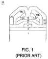
- FIG. 1depicts a cross-sectional schematic view of a thin film transistor 22 being a type that has a bottom gate structure.
- the thin film transistor 22includes a glass substrate 1 having an underlayer 2 formed on the surface thereof.
- a gateis formed on the underlayer 2 .
- the gatecomprises a gate metal layer 4 and a gate dielectric 8 .
- the gatecontrols the movement of charge carriers in the transistor.
- a gate dielectric 8 formed over the gate metal layer 4electrically isolates the gate from semiconductor layers 10 , 14 a , 14 b , formed thereon, each of which may function to provide charge carriers to the transistor.
- a source region 18 a of the transistoris formed on semiconductor layer 14 a and a drain region 18 b of the transistor is formed on semiconductor layer 14 b .
- a passivation layer 20encapsulates the thin film transistor 22 to protect it from environmental hazards such as moisture and oxygen.
- Amorphous siliconin particular, is widely employed because it is easy to deposit at low temperatures using techniques such as, for example, plasma enhanced chemical vapor deposition (PECVD). Unfortunately, it is difficult to deposit amorphous silicon layers that are continuous (e.g., without gaps or voids) using PECVD techniques. Amorphous silicon layers also tend to have a lower electron mobility. A low electron mobility for the amorphous silicon may limit the speed of transistors formed therefrom.
- PECVDplasma enhanced chemical vapor deposition
- polycrystalline siliconhas been actively investigated as a substitute for amorphous silicon in thin film transistors.
- Polycrystalline siliconalso has an electron mobility several orders of magnitude greater than that of amorphous silicon, which allows for the formation of fast-switching thin film transistors.
- PECVDplasma enhanced chemical vapor deposition
- some transistor fabrication processesform polycrystalline silicon by first depositing a layer of amorphous silicon at relatively low temperatures and then annealing the layer using a laser or a furnace to convert the amorphous silicon to polycrystalline silicon. While the electron mobility is higher for polycrystalline silicon films formed using an annealing process than for an amorphous silicon film, the electron mobility of such films is still lower than the electron mobility for polycrystalline silicon films directly deposited on a substrate from a plasma enhanced chemical vapor deposition (PECVD) process. Furthermore, annealing requires an additional step, thereby reducing the process throughput of thin film transistor fabrication processes.
- PECVDplasma enhanced chemical vapor deposition
- a method of silicon layer deposition for thin film transistor applications for use in active matrix liquid crystal displaysis described.
- a silicon layeris deposited using a cyclical deposition process.
- the cyclical deposition processcomprises alternately adsorbing a silicon-containing precursor and a reducing gas on a substrate structure.
- the adsorbed silicon-containing precursorreacts with the adsorbed reducing gas to form the silicon layer on the substrate.
- the method of silicon layer deposition formed with the cyclical deposition processmay also be used in conjunction with other deposition processes.
- a silicon seed layermay be formed on a substrate using a cyclical deposition process followed by a bulk silicon layer formed using a chemical vapor deposition (CVD) process.
- CVDchemical vapor deposition
- Thin film transistorssuch as for example a bottom-gate transistor or a top-gate transistor, including one or more silicon layers may be formed using such cyclical deposition techniques.
- a preferred process sequence for fabricating a bottom-gate transistorincludes providing a substrate having a gate comprising a gate metal layer and a gate dielectric layer formed thereon.
- One or more silicon layersare deposited on the gate dielectric layer.
- the one or more silicon layersmay comprise, for example, a source region and/or a drain region of the transistor.
- the one or more silicon layersare formed by alternately adsorbing a silicon-containing precursor and a reducing gas on the substrate.
- the adsorbed silicon-containing precursorreacts with the adsorbed reducing gas to form the silicon layer on the substrate.
- the bottom-gate transistormay be completed by depositing a passivation layer on the substrate.
- FIG. 1depicts a cross-sectional schematic view of a prior art bottom-gate thin film transistor
- FIG. 2depicts a schematic, cross-sectional view of a process chamber that can be used to practice embodiments described herein;
- FIG. 3illustrates a process sequence for silicon layer formation using cyclical deposition techniques according to one embodiment described herein;
- FIG. 4illustrates a process sequence for silicon layer formation using cyclical deposition techniques according to an alternative embodiment described herein;
- FIGS. 5A-5Bdepict alternate embodiments of cyclical deposition techniques according to embodiments described herein including one or more pulses of a dopant compound
- FIGS. 6A-6Ddepict cross-sectional views of a substrate at different stages of a bottom-gate thin film transistor fabrication sequence.
- FIGS. 7A-7Ddepict cross-sectional views of a substrate at different stages of a top-gate thin film transistor fabrication sequence.
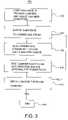
- FIG. 2depicts a schematic cross-sectional view of a process chamber 310 that can be used to perform integrated circuit fabrication in accordance with embodiments described herein.
- the process chamber 310generally houses a substrate support pedestal 348 , which is used to support a substrate (not shown).
- the substrate support pedestal 348is movable in a vertical direction inside the process chamber 310 using a displacement mechanism 348 a.
- the substratecan be heated to some desired temperature prior to or during deposition.
- the substrate support pedestal 348may be heated using an embedded heater element 352 a .
- the substrate support pedestal 348may be resistively heated by applying an electric current from an AC power supply 352 to the heater element 352 a .
- the substrate(not shown) is, in turn, heated by the pedestal 348 .
- the substrate support pedestal 348may be heated using radiant heaters such as, for example, lamps (not shown).
- a temperature sensor 350 asuch as a thermocouple, is also embedded in the substrate support pedestal 348 to monitor the temperature of the pedestal 348 in a conventional manner. The measured temperature is used in a feedback loop to control the AC power supply 352 for the heating element 352 a , such that the substrate temperature can be maintained or controlled at a desired temperature which is suitable for the particular process application.
- a vacuum pump 318is used to evacuate the process chamber 310 and to maintain the pressure inside the process chamber 310 .
- a gas manifold 334through which process gases are introduced into the process chamber 310 , is located above the substrate support pedestal 348 .
- the gas manifold 334is connected to a gas panel 311 , which controls and supplies various process gases to the process chamber 310 .
- Proper control and regulation of the gas flows to the gas manifold 334are performed by mass flow controllers (not shown) and a microprocessor controller 370 .
- the gas manifold 334allows process gases to be introduced and uniformly distributed in the process chamber 310 . Additionally, the gas manifold 334 may optionally be heated to prevent condensation of the any reactive gases within the manifold.
- the gas manifold 334includes a plurality of electronic control valves (not shown).
- the electronic control valves as used hereinrefer to any control valve capable of providing rapid and precise gas flow to the process chamber 310 with valve open and close cycles of less than about 1-2 seconds, and more preferably less than about 0.1 second.
- the microprocessor controller 370may be one of any form of general purpose computer processor (CPU) 371 that can be used in an industrial setting for controlling various chambers and sub-processors.
- the computermay use any suitable memory 372 , such as random access memory, read only memory, floppy disk drive, hard disk, or any other form of digital storage, local or remote.
- Various support circuits 373may be coupled to the CPU for supporting the processor in a conventional manner.
- Software routines as requiredmay be stored on the memory or executed by a second CPU that is remotely located.
- the software routinesare executed to initiate process recipes or sequences.
- the software routineswhen executed, transform the general purpose computer into a specific process computer that controls the chamber operation so that a chamber process is performed.
- software routinesmay be used to precisely control the activation of the electronic control valves for the execution of process sequences according to the present invention.
- the software routinesmay be performed in hardware, as an application specific integrated circuit or other type of hardware implementation, or a combination of software or hardware.
- process chamber 310may be adapted to generate an electric field therein.
- the electric fieldmay be applied to one or more of the process gases introduced into the process chamber 310 through the gas manifold 334 .
- a high frequency power supply 312may be coupled to the substrate support pedestal 348 .
- the high frequency power supply 312may be a radio frequency (RF) power supply with a frequency of, for example, about 13.56 MHz.
- An electric fieldmay be generated within the process chamber 310 by applying a high frequency power to the substrate support pedestal 348 .
- the electric fieldmay be used to ignite a process gas, such as, for example a reducing gas, forming a plasma 314 within the process chamber 310 .
- the plasma 314is believed to enhance the reaction between adsorbed process gases on a substrate positioned on the substrate support pedestal 348 .
- the plasmamay optionally be generated in a remote plasma chamber (not shown) that may then be introduced into the process chamber 310 through the gas manifold 334 .
- a method of silicon layer deposition for thin film transistor applicationsis described.
- the silicon layeris deposited using a cyclical deposition process.
- the cyclical deposition processcomprises alternately adsorbing a silicon-containing precursor and a reducing gas on a substrate structure.
- the silicon-containing precursor and the reducing gasreact to form a silicon layer on the substrate.
- FIG. 3illustrates a process sequence 400 detailing the various steps used for the deposition of the silicon layer. These steps may be performed in a process chamber similar to that described above with reference to FIG. 2 .
- a substrateis provided to the process chamber.
- the substratemay be for example, a glass or clear plastic material suitable for AMLCD fabrication.
- the process chamber conditionssuch as, for example, the temperature and pressure are adjusted to enhance the adsorption of the process gases on the substrate to facilitate the reaction of the silicon-containing precursor and the reducing gas.
- the substrateshould be maintained at a temperature between about 100° C. and about 600° C. at a process chamber pressure of between about 10 millitorr and about 10 torr.
- a carrier gas streamis established within the process chamber as indicated in step 404 .
- Carrier gasesmay be selected so as to also act as a purge gas for removal of volatile reactants and/or by-products from the process chamber.
- Carrier gasessuch as, for example, helium (He), argon (Ar), and combinations thereof, may be used.
- a pulse of a silicon-containing precursoris added to the carrier gas stream.
- the term pulse as used hereinrefers to a dose of material injected into the process chamber or into the carrier gas stream.
- the pulse of the silicon-containing precursorlasts for a predetermined time interval.
- the silicon-containing precursormay comprise, for example, silane (SiH 4 ), disilane (Si 2 H 6 ), silicon tetrachloride (SiCl 4 ), dichlorosilane (Si 2 Cl 2 H 2 ) and trichlorosilane (SiCl 3 H), among others.
- the time interval for the pulse of the silicon-containing precursoris variable depending upon a number of factors such as, for example, the volume capacity of the process chamber employed, the vacuum system coupled thereto and the volatility/reactivity of the reactants used. For example, (1) a large-volume process chamber may lead to a longer time to stabilize the process conditions such as, for example, carrier/purge gas flow and temperature, requiring a longer pulse time; (2) a lower flow rate for the process gas may also lead to a longer time to stabilize the process conditions requiring a longer pulse time; and (3) a lower chamber pressure means that the process gas is evacuated from the process chamber more quickly requiring a longer pulse time.
- the process conditionsare advantageously selected so that a pulse of the silicon-containing precursor provides a sufficient amount of precursor, such that at least a monolayer of the silicon-containing precursor is adsorbed on the substrate. Thereafter, excess silicon-containing precursor remaining in the chamber may be removed from the process chamber by the constant carrier gas stream in combination with the vacuum system.
- a pulse of a reducing gasis added to the carrier gas stream.
- Suitable reducing gasesmay include, for example, hydrogen (H 2 ), borane (BH 3 ) and diborane (B 2 H 6 ), among others.
- the pulse of the reducing gasalso lasts for a predetermined time interval.
- the time interval for the pulse of the reducing gasshould be long enough to provide a sufficient amount of the reducing gas for reaction with the silicon-containing precursor that is already adsorbed on the substrate. Thereafter, excess reducing gas is flushed from the process chamber by the carrier gas stream.
- a high frequency powersuch as an RF power
- RF powermay be applied to the substrate support pedestal 348 ( FIG. 2 ) coincident with the pulse of the reducing gas (step 408 ) to generate a plasma comprising the reducing gas within the process chamber.
- the plasmais believed to enhance the reaction between the adsorbed silicon-containing precursor on the substrate and the reducing gas.
- the application of the high frequency power to the substrate support chambermay last for the same predetermined time interval as the time interval for the pulse of the reducing gas.
- a high frequency powerof about 0.2 W/mm 2 to about 2 W/mm 2 may be applied to the substrate support pedestal.
- Steps 404 through 408comprise one embodiment of a deposition cycle for a silicon layer.
- a constant flow of carrier gasis provided to the process chamber modulated by alternating periods of pulsing and non-pulsing where the periods of pulsing alternate between the silicon-containing precursor and the reducing gas along with the carrier gas stream, while the periods of non-pulsing include only the carrier gas stream.
- the time interval for each of the pulses of the silicon-containing precursor and the reducing gasmay have the same duration. That is the duration of the pulse of the silicon-containing precursor may be identical to the duration of the pulse of the reducing gas.
- a time interval (T 1 ) for the pulse of the silicon-containing precursoris equal to a time interval (T 2 ) for the pulse of the reducing gas.
- the time interval for each of the pulses of the silicon-containing precursor and the reducing gasmay have different durations. That is the duration of the pulse of the silicon-containing precursor may be shorter or longer than the duration of the pulse of the reducing gas.
- a time interval (T 1 ) for the pulse of the silicon-containing precursoris different than a time interval (T 2 ) for the pulse of the reducing gas.
- the periods of non-pulsing between each of the pulses of the silicon-containing precursor and the reducing gasmay have the same duration. That is the duration of the period of non-pulsing between each pulse of the silicon-containing precursor and each pulse of the reducing gas is identical.
- a time interval (T 3 ) of non-pulsing between the pulse of the silicon-containing precursor and the pulse of the reducing gasis equal to a time interval (T 4 ) of non-pulsing between the pulse of the reducing gas and the pulse of the silicon-containing precursor.
- the periods of non-pulsing between each of the pulses of the silicon-containing precursor and the reducing gasmay have different durations. That is the duration of the period of non-pulsing between each pulse of the silicon-containing precursor and each pulse of the reducing gas may be shorter or longer than the duration of the period of non-pulsing between each pulse of the reducing gas and the silicon-containing precursor.
- a time interval (T 3 ) of non-pulsing between the pulse of the silicon-containing precursor and the pulse of the reducing gasis different from a time interval (T 4 ) of non-pulsing between the pulse of the reducing gas and the pulse of the silicon-containing precursor.
- time intervals for each pulse of the silicon-containing precursor, the reducing gas and the periods of non-pulsing therebetween for each deposition cyclemay have the same duration.
- a time interval (T 1 ) for the silicon-containing precursor, a time interval (T 2 ) for the reducing gas, a time interval (T 3 ) of non-pulsing between the pulse of the silicon-containing precursor and the pulse of the reducing gas and a time interval (T 4 ) of non-pulsing between the pulse of the reducing gas and the pulse of the silicon-containing precursoreach have the same value for each subsequent deposition cycle.
- a time interval (T 1 ) for the pulse of the silicon-containing precursorhas the same duration as the time interval (T 1 ) for the pulse of the silicon-containing precursor in subsequent deposition cycles (C 2 . . . C N ).
- the duration of each pulse of the reducing gas and the periods of non-pulsing between the pulse of the silicon-containing precursor and the reducing gas in deposition cycle (C 1 )is the same as the duration of each pulse of the reducing gas and the periods of non-pulsing between the pulse of the silicon-containing precursor and the reducing gas in subsequent deposition cycles (C 2 . . . C N ), respectively.
- the time intervals for at least one pulse of the silicon-containing precursor, the reducing gas and the periods of non-pulsing therebetween for one or more of the deposition cycles of the silicon layer deposition processmay have different durations.
- one or more of the time intervals (T 1 ) for the pulses of the silicon-containing precursor, the time intervals (T 2 ) for the pulses of the reducing gas, the time intervals (T 3 ) of non-pulsing between the pulse of the silicon-containing precursor and the pulse of the reducing gas and the time intervals (T 4 ) of non-pulsing between the pulse of the reducing gas and the pulse of the silicon-containing precursormay have different values for one or more subsequent deposition cycles of the silicon layer deposition process.
- the time interval (T 1 ) for the pulse of the silicon-containing precursormay be longer or shorter than the time interval (T 1 ) for the pulse of the silicon-containing precursor in a subsequent deposition cycle (C 2 . . . C N ).
- the duration of each pulse of the reducing gas and the periods of non-pulsing between the pulse of the silicon-containing precursor and the pulse of the reducing gas in deposition cycle (C 1 )may be the same or different than the duration of each pulse of the reducing gas and the periods of non-pulsing between the pulse of the silicon-containing precursor and the reducing gas in subsequent deposition cycles (C 2 . . . C N ), respectively.
- step 410after each deposition cycle (steps 404 through 408 ) a total thickness of the silicon layer will be formed on the substrate. Depending on specific device requirements, subsequent deposition cycles may be needed to achieve a desired thickness. As such, steps 404 through 408 are repeated until the desired thickness for the silicon layer is achieved. Thereafter, when the desired thickness for the silicon layer is achieved the process is stopped as indicated by step 412 .
- the silicon layer deposition cyclecomprises separate pulses for each of the silicon-containing precursor, the reducing gas, and a purge gas.
- the silicon layer deposition sequence 500includes providing a substrate to the process chamber (step 502 ), providing a first pulse of a purge gas to the process chamber (step 504 ), providing a pulse of a silicon-containing precursor to the process chamber (step 506 ), providing a second pulse of the purge gas to the process chamber (step 508 ), providing a pulse of a reducing gas to the process chamber (step 510 ), and then repeating steps 504 through 510 or stopping the deposition process (step 514 ) depending on whether a desired thickness for the silicon layer has been achieved (step 512 ).
- a high frequency powersuch as an RF power
- RF powermay be applied to the substrate support pedestal 348 ( FIG. 2 ) coincident with the pulse of the reducing gas (step 510 ) to generate a plasma comprising the reducing gas within the process chamber.
- the plasmais believed to enhance the reaction between the adsorbed silicon-containing precursor on the substrate and the reducing gas.
- the application of the high frequency power to the substrate support chambermay last for the same predetermined time interval as the time interval for the pulse of the reducing gas.
- a high frequency powerof about 0.2 W/mm 2 to about 2 W/mm 2 may be applied to the substrate support pedestal.
- the time intervals for each of the pulses of the silicon-containing precursor, the reducing gas and the purge gasmay have the same or different durations as discussed above with respect to FIG. 3 .
- the time intervals for at least one pulse of the silicon-containing precursor, the reducing gas and the purge gas for one or more of the deposition cycles of the silicon layer deposition processmay have different durations.
- the silicon layer deposition cycleis depicted as beginning with a pulse of the silicon-containing precursor followed by a pulse of the reducing gas.
- the silicon layer deposition cyclemay start with a pulse of the reducing gas followed by a pulse of the silicon-containing precursor.
- the reducing gasmay become incorporated, at least in part, into the silicon layer.
- hydrogen present in the reducing gasmay become bound to the silicon, thereby forming a hydrogenated silicon (Si:H) layer.
- a silicon seed layermay be formed on a substrate using a cyclical deposition process.
- the silicon seed layermay have a thickness of less than about 50 ⁇ .
- a bulk silicon layermay be formed on the silicon seed layer using a chemical vapor deposition (CVD) process.
- the bulk silicon layermay have a thickness up to about 2000 ⁇ .
- One exemplary process of depositing a silicon layercomprises alternately providing pulses of silane (SiH 4 ) and pulses of hydrogen (H 2 ).
- the silane (SiH 4 )may be provided to an appropriate flow control valve, for example, an electronic flow control valve, at a flow rate of between about 10 sccm (standard cubic centimeters per minute) and about 100 sccm, and thereafter pulsed for about 0.5 seconds or less.
- a carrier gas comprising argon (Ar)is provided along with the silane at a flow rate between about 10 sccm to about 100 sccm.
- the hydrogen (H 2 )may be provided to an appropriate flow control valve, for example, an electronic flow control valve, at a flow rate of between about 10 sccm and about 1000 sccm, and thereafter pulsed for about 0.5 seconds or less.
- a carrier gas comprising argon (Ar)is provided along with the reducing gas at a flow rate between about 10 sccm to about 1000 sccm.
- the substratemay be maintained at a chamber pressure between about 10 millitorr to about 10 torr.
- the above mentioned flow rates for the carrier gas, the silicon-containing precursor, and the reducing gasmay be varied, depending upon the volume capacity of the process chamber 310 .
- the substrate temperaturedetermines whether amorphous silicon or polycrystalline silicon material is formed. For example, if the substrate temperature is maintained between about 100° C. to about 400° C., an amorphous silicon layer is deposited on the substrate. However, if the substrate temperature is maintained between about 400° C. to about 600° C., a polycrystalline silicon layer will be deposited on the substrate. Furthermore, the amorphous silicon layer may be optionally converted to a polysilicon layer using, for example, a laser annealing process or a metal induced crystallization process, among others.
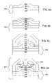
- Another exemplary process of depositing a silicon layercomprises alternately providing pulses of a silicon-containing precursor, pulses of a dopant compound and pulses of a reducing gas.
- the dopant compoundmay be mixed with the silicon-containing precursor and pulses of the silicon-containing precursor/dopant compound may be provided to the process chamber.
- the dopant compoundmay be an n-type dopant or a p-type dopant for the silicon layer.
- Each pulse of the silicon-containing precursor/dopant compoundmay comprise about 1% to about 10% of the dopant compound.
- one or more pulses of the dopant compound 530may be provided coincident with the pulses of the silicon-containing precursor 535 .
- the time duration for each pulse of the dopant compoundmay last for a predetermined time interval that is less than the time interval for the pulse of the silicon-containing precursor, such that more than one pulse of the dopant compound may be provided coincident with a pulse of the silicon-containing precursor.
- the flow rate for the one or more pulses of the dopant compoundmay be, for example, about 1% to about 10% of the flow rate for the pulse of the silicon-containing precursor.
- one or more pulses of the dopant compound 540may be provided coincident with the pulses of the reducing gas 545 .
- the time duration for each pulse of the dopant compoundmay last for a predetermined time interval that is less than the time interval for the pulse of the reducing gas, such that more than one pulse of the dopant compound may be provided coincident with a pulse of the reducing gas.
- the flow rate for the one or more pulses of the dopant compoundmay be, for example, about 1% to about 10% of the flow rate for the pulse of the reducing gas.
- Suitable n-type dopant compoundsinclude, for example, arsenic-based compounds and phosphorus-based compounds, such as arsine (AsH 3 ) and phosphine (PH 3 ), among others.
- Suitable p-type dopant compoundsinclude, for example, boron-based compounds such as, boron trihydride (BH 3 ), among others.
- FIGS. 6A-6Dillustrate cross-sectional schematic views of substrate structure 650 during different stages of a bottom-gate thin film transistor fabrication sequence incorporating a silicon layer formed using a cyclical deposition process.
- This transistor fabrication sequenceis for a switch in an active matrix liquid crystal display (AMLCD) and this process depicts the formation of one of an array of switches used in an AMLCD.
- FIG. 6Aillustrates a cross-sectional view of a substrate 600 .
- the substrate 600may comprise a material that is essentially optically transparent in the visible spectrum, such as, for example, glass or clear plastic, including soda-lime glass, borosilicate glass, or quartz glass.
- the substratemay be of varying shapes or dimensions.
- the substrateis a glass substrate with dimensions greater than about 500 mm ⁇ 500 mm.
- the substrate 600may have an underlayer 602 thereon.
- the underlayer 602may be an insulating material, for example, such as silicon dioxide (SiO 2 ) or silicon nitride (SiN).
- the underlayer 602may be formed using conventional deposition techniques.
- a gate metal layer 604is formed on the underlayer 602 .
- the gate metal layer 604comprises an electrically conductive layer that controls the movement of charge carriers within the thin film transistor.
- the gate metal layer 604may comprise a metal such as, for example, aluminum (Al), tungsten (W), chromium (Cr), tantalum (Ta), or combinations thereof, among others.
- the gate metal layer 604may be formed using conventional deposition, lithography and etching techniques.
- a gate dielectric layer 608is formed on the gate metal layer 604 .
- the gate dielectric layer 608may comprise, for example, silicon dioxide (SiO 2 ), silicon nitride (SiN), aluminum oxide (Al 2 O 3 ), tantalum oxide (Ta 2 O 5 ), among others.
- the gate dielectric material 608has a thickness in the range of about 20 Angstroms to about 5000 Angstroms.
- a silicon bulk layer 610is deposited on the gate dielectric layer 608 .
- the silicon bulk layer 610may comprise amorphous silicon deposited using an embodiment of the cyclical deposition technique described above with reference to FIGS. 3-4 .
- Silicon bulk layer 610may be deposited to a thickness within a range of about 20 Angstroms to about 2000 Angstroms.
- the cyclical deposition techniques employed for the silicon bulk layer 610 depositionprovide conformal step coverage on the gate dielectric material 608 .
- a silicon seed layer 609may be deposited prior to the silicon bulk layer 610 deposition.
- the silicon seed layermay be formed using an embodiment of the cyclical deposition techniques described above with reference to FIGS. 3-4 .
- the silicon bulk layer 610may be deposited thereon using conventional deposition techniques such as, for example, chemical vapor deposition (CVD) or plasma enhanced chemical vapor deposition (PECVD).
- CVDchemical vapor deposition
- PECVDplasma enhanced chemical vapor deposition
- an etch stop layer 612may be deposited on silicon bulk layer 610 .
- the etch stop layer 612may comprise an insulating material such as, for example, silicon nitride (SiN).
- the etch stop layer 612may be formed using, for example, plasma enhanced chemical vapor deposition, chemical vapor deposition, physical vapor deposition, or other conventional methods known to the art.
- the etch stop layer 612 and the silicon bulk layer 610are lithographically patterned and etched using conventional techniques.
- a doped silicon layer 614is formed on the patterned etch stop layer 612 and silicon bulk layer 610 .
- the doped silicon layer 614may be deposited using an embodiment of the cyclical deposition process described above with reference to FIGS. 3-5 .
- the doped silicon layer 614may be deposited to a thickness within a range of about 10 Angstroms to about 100 Angstroms.
- the cyclical deposition techniques employed for the doped silicon layer 614 depositionprovide conformal step coverage on the patterned etch stop layer 612 and the silicon bulk layer 610 .
- the doped silicon layer 614directly contacts portions of the silicon bulk layer 610 , forming a semiconductor junction.
- Conductive layer 618is formed on the doped silicon layer 614 .
- Conductive layer 618may comprise a metal such as, for example, aluminum (Al), tungsten (W), molybdenum (Mo), chromium (Cr), tantalum (Ta), and combinations thereof, among others.
- the conductive layer 618may be formed using conventional deposition techniques.
- both the conductive layer 618 and the doped silicon layer 614may be lithographically patterned to define a source region 614 a and a drain region 614 b as well as a source contact 618 a and a drain contact 618 b .
- the source 614 a and drain 614 b regions of the thin film transistorare separated from one another by the stop etch layer 612 .
- a passivation layer 620may be deposited atop the substrate structure 650 .
- Passivation layer 620conformally coats exposed surfaces of gate dielectric layer 608 , source contact 618 a , drain contact 618 b and etch stop layer 612 .
- the passivation layer 620is generally an insulator and may comprise, for example, silicon oxide or silicon nitride.
- the passivation layer 620may be formed using conventional deposition techniques.
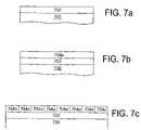
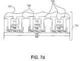
- FIGS. 7A-7Dillustrate cross-sectional schematic views of substrate structure 750 during different stages of a top-gate thin film transistor fabrication sequence incorporating a silicon layer formed using a cyclical deposition process.
- the top-gate thin film transistormay be, for example, a metal-oxide-semiconductor field effect transistor (MOSFET) or a junction field effect transistor (JFET).
- MOSFETmetal-oxide-semiconductor field effect transistor
- JFETjunction field effect transistor
- FIG. 7Aillustrates a cross-sectional view of a substrate 700 .
- the substratemay comprise a material that is essentially optically transparent in the visible spectrum, such as, for example, glass or clear plastic, including soda-lime glass, borosilicate glass, or quartz.
- the substratemay have an underlayer 702 thereon.
- the underlayer 702may be an insulating material, such as, for example, silicon dioxide (SiO 2 ) or silicon nitride (SiN).
- an n-type doped silicon layer 704 nis deposited on the underlayer 702 .
- the n-type doped silicon layer 704 nmay be formed using an embodiment of the cyclical deposition process described above with reference to FIGS. 3-5 .
- the silicon layermay be a p-type doped layer.
- n-type doped silicon layer 704 nAfter the n-type doped silicon layer 704 n is formed selected portions thereof are ion implanted to form p-type doped regions 704 p adjacent to n-type doped regions 704 n , as shown in FIG. 7C .
- the interfaces between n-type regions 704 n and p-type regions 704 pare semiconductor junctions that support the ability of the thin film transistor to act as a switching device.
- ion doping portions of semiconductor layer 704one or more semiconductor junctions are formed, with an intrinsic electrical potential present across each junction.
- a gate dielectric layer 708is deposited on the n-type doped regions 704 n and the p-type doped regions 704 p .
- the gate dielectric layer 708may comprise, for example, silicon dioxide (SiO 2 ), silicon nitride (SiN), aluminum oxide (Al 2 O 3 ), and tantalum pentoxide (Ta 2 O 5 ), among others.
- the gate dielectric layer 708may be formed using conventional deposition processes.
- a gate metal layer 710is deposited on the gate dielectric layer 708 .
- the gate metal layer 710comprises an electrically conductive layer that controls the movement of charge carriers within the thin film transistor.
- the gate metal layer 710may comprise a metal such as, for example, aluminum (Al), tungsten (W), chromium (Cr), tantalum (Ta), or combinations thereof, among others.
- the gate metal layer 710may be formed using conventional deposition techniques. After deposition, the gate metal layer 710 is patterned to define gates using conventional lithography and etching techniques.
- an interlayer dielectric 712is formed thereon.
- the interlayer dielectric 712may comprise, for example, an oxide such as silicon dioxide.
- Interlayer dielectric 712may be formed using conventional deposition processes.
- the interlayer dielectric 712is patterned to expose the n-type doped regions 704 n and the p-type doped regions 704 p .
- the patterned regions of the interlayer dielectric 712are filled with a conductive material to form contacts 720 .
- the contacts 720may comprise a metal such as, for example, aluminum (Al), tungsten (W), molybdenum (Mo), chromium (Cr), tantalum (Ta), and combinations thereof, among others.
- the contacts 720may be formed using conventional deposition techniques.
- a passivation layer 722may be formed thereon in order to protect and encapsulate a completed thin film transistor 725 .
- the passivation layer 722is generally an insulator and may comprise, for example, silicon oxide or silicon nitride.
- the passivation layer 722may be formed using conventional deposition techniques.
- FIGS. 7A-7Das well as the supporting discussion provide an embodiment in which the doped silicon layer 704 is an n-type silicon layer with p-type dopant ions implanted therein, one skilled in the art will recognize that other configurations are within the scope of the invention. For example, one may deposit a p-type silicon layer and implant n-type dopant ions in regions thereof.
- the switch for an AMLCDmay be any variety of bipolar or unipolar transistor devices wherein a silicon layer is deposited using the cyclical deposition process described herein.
Landscapes
- Chemical & Material Sciences (AREA)
- Engineering & Computer Science (AREA)
- Mechanical Engineering (AREA)
- Chemical Kinetics & Catalysis (AREA)
- General Chemical & Material Sciences (AREA)
- Materials Engineering (AREA)
- Metallurgy (AREA)
- Organic Chemistry (AREA)
- Inorganic Chemistry (AREA)
- Physics & Mathematics (AREA)
- Electromagnetism (AREA)
- Plasma & Fusion (AREA)
- Chemical Vapour Deposition (AREA)
- Thin Film Transistor (AREA)
- Liquid Crystal (AREA)
Abstract
Description
This application claims priority from U.S. Provisional Application Ser. No. 60/368,402 filed Mar. 26, 2002 entitled, “Deposition Of Gate Dielectric Layers For Active Matrix Liquid Crystal Display (AMLCD) Applications.”
1. Field of the Invention
Embodiments of the present invention relate to methods of silicon layer deposition and, more particularly, to methods of silicon layer formation using cyclical deposition techniques for active matrix liquid crystal display (AMLCD) applications.
2. Description of the Background Art
Active matrix liquid crystal displays have eliminated many problems associated with passive displays. For example, the fabrication of active matrix liquid crystal displays have enabled display screens to achieve greater brightness, enhanced readability, a greater variety of color shades, and broader viewing angles compared to displays that employ other technologies. Active matrix liquid crystal displays have therefore become the display technology of choice for numerous applications including computer monitors, television screens, camera displays, avionics displays, as well as numerous other applications.
Active matrix liquid crystal displays generally comprise an array of picture elements called pixels. An electronic switch is associated with each pixel in the display to control the operation thereof. Various electronic switches such as, for example, thin film transistors, and organic light emitting diodes (OLED), among others have been investigated to control pixel operation. Thin film transistors, in particular, offer a high degree of design flexibility and device performance.
Thin film transistors are generally formed on large area substrates having a high degree of optical transparency such as, for example, glass.FIG. 1 depicts a cross-sectional schematic view of athin film transistor 22 being a type that has a bottom gate structure. Thethin film transistor 22 includes aglass substrate 1 having anunderlayer 2 formed on the surface thereof. A gate is formed on theunderlayer 2. The gate comprises agate metal layer 4 and a gate dielectric8. The gate controls the movement of charge carriers in the transistor. A gate dielectric8 formed over thegate metal layer 4 electrically isolates the gate fromsemiconductor layers source region 18aof the transistor is formed onsemiconductor layer 14aand adrain region 18bof the transistor is formed onsemiconductor layer 14b. Finally, apassivation layer 20 encapsulates thethin film transistor 22 to protect it from environmental hazards such as moisture and oxygen.
Many thin film transistors use silicon for thesemiconductor layers
As such, polycrystalline silicon has been actively investigated as a substitute for amorphous silicon in thin film transistors. Polycrystalline silicon also has an electron mobility several orders of magnitude greater than that of amorphous silicon, which allows for the formation of fast-switching thin film transistors.
Unfortunately, conventional plasma enhanced chemical vapor deposition (PECVD) techniques used to form polycrystalline silicon tend to be high temperature processes. High deposition temperatures may not be compatible with the glass substrates upon which the thin film transistors are formed, since the glass tends to soften and become dimensionally unstable.
To circumnavigate this problem, some transistor fabrication processes form polycrystalline silicon by first depositing a layer of amorphous silicon at relatively low temperatures and then annealing the layer using a laser or a furnace to convert the amorphous silicon to polycrystalline silicon. While the electron mobility is higher for polycrystalline silicon films formed using an annealing process than for an amorphous silicon film, the electron mobility of such films is still lower than the electron mobility for polycrystalline silicon films directly deposited on a substrate from a plasma enhanced chemical vapor deposition (PECVD) process. Furthermore, annealing requires an additional step, thereby reducing the process throughput of thin film transistor fabrication processes.
Therefore, a need exists to develop a method of forming silicon layers for use in thin film transistors.
A method of silicon layer deposition for thin film transistor applications for use in active matrix liquid crystal displays (AMLCD) is described. A silicon layer is deposited using a cyclical deposition process. The cyclical deposition process comprises alternately adsorbing a silicon-containing precursor and a reducing gas on a substrate structure. The adsorbed silicon-containing precursor reacts with the adsorbed reducing gas to form the silicon layer on the substrate.
The method of silicon layer deposition formed with the cyclical deposition process may also be used in conjunction with other deposition processes. For example, a silicon seed layer may be formed on a substrate using a cyclical deposition process followed by a bulk silicon layer formed using a chemical vapor deposition (CVD) process.
Thin film transistors, such as for example a bottom-gate transistor or a top-gate transistor, including one or more silicon layers may be formed using such cyclical deposition techniques. In one embodiment, a preferred process sequence for fabricating a bottom-gate transistor includes providing a substrate having a gate comprising a gate metal layer and a gate dielectric layer formed thereon. One or more silicon layers are deposited on the gate dielectric layer. The one or more silicon layers may comprise, for example, a source region and/or a drain region of the transistor. The one or more silicon layers are formed by alternately adsorbing a silicon-containing precursor and a reducing gas on the substrate. The adsorbed silicon-containing precursor reacts with the adsorbed reducing gas to form the silicon layer on the substrate. Thereafter, the bottom-gate transistor may be completed by depositing a passivation layer on the substrate.
So that the manner in which the above recited features of the present invention are attained and can be understood in detail, a more particular description of the invention, briefly summarized above, may be had by reference to the embodiments thereof which are illustrated in the appended drawings.
It is to be noted, however, that the appended drawings illustrate only typical embodiments of this invention and are therefore not to be considered limiting of its scope, for the invention may admit to other equally effective embodiments.
Depending on the specific process, the substrate can be heated to some desired temperature prior to or during deposition. For example, thesubstrate support pedestal 348 may be heated using an embeddedheater element 352a. Thesubstrate support pedestal 348 may be resistively heated by applying an electric current from anAC power supply 352 to theheater element 352a. The substrate (not shown) is, in turn, heated by thepedestal 348. Alternatively, thesubstrate support pedestal 348 may be heated using radiant heaters such as, for example, lamps (not shown).
A temperature sensor350a, such as a thermocouple, is also embedded in thesubstrate support pedestal 348 to monitor the temperature of thepedestal 348 in a conventional manner. The measured temperature is used in a feedback loop to control theAC power supply 352 for theheating element 352a, such that the substrate temperature can be maintained or controlled at a desired temperature which is suitable for the particular process application.
Avacuum pump 318 is used to evacuate theprocess chamber 310 and to maintain the pressure inside theprocess chamber 310. Agas manifold 334, through which process gases are introduced into theprocess chamber 310, is located above thesubstrate support pedestal 348. Thegas manifold 334 is connected to agas panel 311, which controls and supplies various process gases to theprocess chamber 310.
Proper control and regulation of the gas flows to thegas manifold 334 are performed by mass flow controllers (not shown) and amicroprocessor controller 370. Thegas manifold 334 allows process gases to be introduced and uniformly distributed in theprocess chamber 310. Additionally, thegas manifold 334 may optionally be heated to prevent condensation of the any reactive gases within the manifold.
Thegas manifold 334 includes a plurality of electronic control valves (not shown). The electronic control valves as used herein refer to any control valve capable of providing rapid and precise gas flow to theprocess chamber 310 with valve open and close cycles of less than about 1-2 seconds, and more preferably less than about 0.1 second.
Themicroprocessor controller 370 may be one of any form of general purpose computer processor (CPU)371 that can be used in an industrial setting for controlling various chambers and sub-processors. The computer may use anysuitable memory 372, such as random access memory, read only memory, floppy disk drive, hard disk, or any other form of digital storage, local or remote.Various support circuits 373 may be coupled to the CPU for supporting the processor in a conventional manner. Software routines as required may be stored on the memory or executed by a second CPU that is remotely located.
The software routines are executed to initiate process recipes or sequences. The software routines, when executed, transform the general purpose computer into a specific process computer that controls the chamber operation so that a chamber process is performed. For example, software routines may be used to precisely control the activation of the electronic control valves for the execution of process sequences according to the present invention. Alternatively, the software routines may be performed in hardware, as an application specific integrated circuit or other type of hardware implementation, or a combination of software or hardware.
Alternatively,process chamber 310 may be adapted to generate an electric field therein. The electric field may be applied to one or more of the process gases introduced into theprocess chamber 310 through thegas manifold 334. For example, a highfrequency power supply 312 may be coupled to thesubstrate support pedestal 348. The highfrequency power supply 312 may be a radio frequency (RF) power supply with a frequency of, for example, about 13.56 MHz.
An electric field may be generated within theprocess chamber 310 by applying a high frequency power to thesubstrate support pedestal 348. The electric field may be used to ignite a process gas, such as, for example a reducing gas, forming aplasma 314 within theprocess chamber 310. Theplasma 314 is believed to enhance the reaction between adsorbed process gases on a substrate positioned on thesubstrate support pedestal 348. The plasma may optionally be generated in a remote plasma chamber (not shown) that may then be introduced into theprocess chamber 310 through thegas manifold 334.
Silicon Layer Formation
A method of silicon layer deposition for thin film transistor applications is described. The silicon layer is deposited using a cyclical deposition process. The cyclical deposition process comprises alternately adsorbing a silicon-containing precursor and a reducing gas on a substrate structure. The silicon-containing precursor and the reducing gas react to form a silicon layer on the substrate.
In one embodiment where a constant carrier gas flow is desired, a carrier gas stream is established within the process chamber as indicated instep 404. Carrier gases may be selected so as to also act as a purge gas for removal of volatile reactants and/or by-products from the process chamber. Carrier gases such as, for example, helium (He), argon (Ar), and combinations thereof, may be used.
Referring to step406, after the carrier gas stream is established within the process chamber, a pulse of a silicon-containing precursor is added to the carrier gas stream. The term pulse as used herein refers to a dose of material injected into the process chamber or into the carrier gas stream. The pulse of the silicon-containing precursor lasts for a predetermined time interval. The silicon-containing precursor may comprise, for example, silane (SiH4), disilane (Si2H6), silicon tetrachloride (SiCl4), dichlorosilane (Si2Cl2H2) and trichlorosilane (SiCl3H), among others.
The time interval for the pulse of the silicon-containing precursor is variable depending upon a number of factors such as, for example, the volume capacity of the process chamber employed, the vacuum system coupled thereto and the volatility/reactivity of the reactants used. For example, (1) a large-volume process chamber may lead to a longer time to stabilize the process conditions such as, for example, carrier/purge gas flow and temperature, requiring a longer pulse time; (2) a lower flow rate for the process gas may also lead to a longer time to stabilize the process conditions requiring a longer pulse time; and (3) a lower chamber pressure means that the process gas is evacuated from the process chamber more quickly requiring a longer pulse time. In general, the process conditions are advantageously selected so that a pulse of the silicon-containing precursor provides a sufficient amount of precursor, such that at least a monolayer of the silicon-containing precursor is adsorbed on the substrate. Thereafter, excess silicon-containing precursor remaining in the chamber may be removed from the process chamber by the constant carrier gas stream in combination with the vacuum system.
Instep 408, after the excess silicon-containing precursor has been sufficiently removed from the process chamber by the carrier gas stream to prevent co-reaction or particle formation with a subsequently provided process gas, a pulse of a reducing gas is added to the carrier gas stream. Suitable reducing gases may include, for example, hydrogen (H2), borane (BH3) and diborane (B2H6), among others.
The pulse of the reducing gas also lasts for a predetermined time interval. In general, the time interval for the pulse of the reducing gas should be long enough to provide a sufficient amount of the reducing gas for reaction with the silicon-containing precursor that is already adsorbed on the substrate. Thereafter, excess reducing gas is flushed from the process chamber by the carrier gas stream.
Alternatively, a high frequency power, such as an RF power, may be applied to the substrate support pedestal348 (FIG. 2 ) coincident with the pulse of the reducing gas (step408) to generate a plasma comprising the reducing gas within the process chamber. The plasma is believed to enhance the reaction between the adsorbed silicon-containing precursor on the substrate and the reducing gas. The application of the high frequency power to the substrate support chamber may last for the same predetermined time interval as the time interval for the pulse of the reducing gas. In general, for silicon layer deposition, a high frequency power of about 0.2 W/mm2to about 2 W/mm2may be applied to the substrate support pedestal.
The time interval for each of the pulses of the silicon-containing precursor and the reducing gas may have the same duration. That is the duration of the pulse of the silicon-containing precursor may be identical to the duration of the pulse of the reducing gas. For such an embodiment, a time interval (T1) for the pulse of the silicon-containing precursor is equal to a time interval (T2) for the pulse of the reducing gas.
Alternatively, the time interval for each of the pulses of the silicon-containing precursor and the reducing gas may have different durations. That is the duration of the pulse of the silicon-containing precursor may be shorter or longer than the duration of the pulse of the reducing gas. For such an embodiment, a time interval (T1) for the pulse of the silicon-containing precursor is different than a time interval (T2) for the pulse of the reducing gas.
In addition, the periods of non-pulsing between each of the pulses of the silicon-containing precursor and the reducing gas may have the same duration. That is the duration of the period of non-pulsing between each pulse of the silicon-containing precursor and each pulse of the reducing gas is identical. For such an embodiment, a time interval (T3) of non-pulsing between the pulse of the silicon-containing precursor and the pulse of the reducing gas is equal to a time interval (T4) of non-pulsing between the pulse of the reducing gas and the pulse of the silicon-containing precursor. During the time periods of non-pulsing only the constant carrier gas stream is provided to the process chamber.
Alternatively, the periods of non-pulsing between each of the pulses of the silicon-containing precursor and the reducing gas may have different durations. That is the duration of the period of non-pulsing between each pulse of the silicon-containing precursor and each pulse of the reducing gas may be shorter or longer than the duration of the period of non-pulsing between each pulse of the reducing gas and the silicon-containing precursor. For such an embodiment, a time interval (T3) of non-pulsing between the pulse of the silicon-containing precursor and the pulse of the reducing gas is different from a time interval (T4) of non-pulsing between the pulse of the reducing gas and the pulse of the silicon-containing precursor. During the time periods of non-pulsing only the constant carrier gas stream is provided to the process chamber.
Additionally, the time intervals for each pulse of the silicon-containing precursor, the reducing gas and the periods of non-pulsing therebetween for each deposition cycle may have the same duration. For such an embodiment, a time interval (T1) for the silicon-containing precursor, a time interval (T2) for the reducing gas, a time interval (T3) of non-pulsing between the pulse of the silicon-containing precursor and the pulse of the reducing gas and a time interval (T4) of non-pulsing between the pulse of the reducing gas and the pulse of the silicon-containing precursor each have the same value for each subsequent deposition cycle. For example, in a first deposition cycle (C1), a time interval (T1) for the pulse of the silicon-containing precursor has the same duration as the time interval (T1) for the pulse of the silicon-containing precursor in subsequent deposition cycles (C2. . . CN). Similarly, the duration of each pulse of the reducing gas and the periods of non-pulsing between the pulse of the silicon-containing precursor and the reducing gas in deposition cycle (C1) is the same as the duration of each pulse of the reducing gas and the periods of non-pulsing between the pulse of the silicon-containing precursor and the reducing gas in subsequent deposition cycles (C2. . . CN), respectively.
Alternatively, the time intervals for at least one pulse of the silicon-containing precursor, the reducing gas and the periods of non-pulsing therebetween for one or more of the deposition cycles of the silicon layer deposition process may have different durations. For such an embodiment, one or more of the time intervals (T1) for the pulses of the silicon-containing precursor, the time intervals (T2) for the pulses of the reducing gas, the time intervals (T3) of non-pulsing between the pulse of the silicon-containing precursor and the pulse of the reducing gas and the time intervals (T4) of non-pulsing between the pulse of the reducing gas and the pulse of the silicon-containing precursor may have different values for one or more subsequent deposition cycles of the silicon layer deposition process. For example, in a first deposition cycle (C1), the time interval (T1) for the pulse of the silicon-containing precursor may be longer or shorter than the time interval (T1) for the pulse of the silicon-containing precursor in a subsequent deposition cycle (C2. . . CN). Similarly, the duration of each pulse of the reducing gas and the periods of non-pulsing between the pulse of the silicon-containing precursor and the pulse of the reducing gas in deposition cycle (C1) may be the same or different than the duration of each pulse of the reducing gas and the periods of non-pulsing between the pulse of the silicon-containing precursor and the reducing gas in subsequent deposition cycles (C2. . . CN), respectively.
Referring to step410, after each deposition cycle (steps 404 through408) a total thickness of the silicon layer will be formed on the substrate. Depending on specific device requirements, subsequent deposition cycles may be needed to achieve a desired thickness. As such,steps 404 through408 are repeated until the desired thickness for the silicon layer is achieved. Thereafter, when the desired thickness for the silicon layer is achieved the process is stopped as indicated bystep 412.
In an alternate process sequence described with respect toFIG. 4 , the silicon layer deposition cycle comprises separate pulses for each of the silicon-containing precursor, the reducing gas, and a purge gas. For such an embodiment, the siliconlayer deposition sequence 500 includes providing a substrate to the process chamber (step502), providing a first pulse of a purge gas to the process chamber (step504), providing a pulse of a silicon-containing precursor to the process chamber (step506), providing a second pulse of the purge gas to the process chamber (step508), providing a pulse of a reducing gas to the process chamber (step510), and then repeatingsteps 504 through510 or stopping the deposition process (step514) depending on whether a desired thickness for the silicon layer has been achieved (step512).
Alternatively, a high frequency power, such as an RF power, may be applied to the substrate support pedestal348 (FIG. 2 ) coincident with the pulse of the reducing gas (step510) to generate a plasma comprising the reducing gas within the process chamber. The plasma is believed to enhance the reaction between the adsorbed silicon-containing precursor on the substrate and the reducing gas. The application of the high frequency power to the substrate support chamber may last for the same predetermined time interval as the time interval for the pulse of the reducing gas. In general, for silicon layer deposition, a high frequency power of about 0.2 W/mm2to about 2 W/mm2may be applied to the substrate support pedestal.
The time intervals for each of the pulses of the silicon-containing precursor, the reducing gas and the purge gas may have the same or different durations as discussed above with respect toFIG. 3 . Alternatively, the time intervals for at least one pulse of the silicon-containing precursor, the reducing gas and the purge gas for one or more of the deposition cycles of the silicon layer deposition process may have different durations.
InFIGS. 3-4 , the silicon layer deposition cycle is depicted as beginning with a pulse of the silicon-containing precursor followed by a pulse of the reducing gas. Alternatively, the silicon layer deposition cycle may start with a pulse of the reducing gas followed by a pulse of the silicon-containing precursor.
The reducing gas may become incorporated, at least in part, into the silicon layer. For example, hydrogen present in the reducing gas may become bound to the silicon, thereby forming a hydrogenated silicon (Si:H) layer.
The method of silicon layer deposition formed with the cyclical deposition process described above with respect toFIGS. 3-4 , may also be used in conjunction with other deposition processes. For example, a silicon seed layer may be formed on a substrate using a cyclical deposition process. The silicon seed layer may have a thickness of less than about 50 Å. Thereafter, a bulk silicon layer may be formed on the silicon seed layer using a chemical vapor deposition (CVD) process. The bulk silicon layer may have a thickness up to about 2000 Å.
One exemplary process of depositing a silicon layer comprises alternately providing pulses of silane (SiH4) and pulses of hydrogen (H2). The silane (SiH4) may be provided to an appropriate flow control valve, for example, an electronic flow control valve, at a flow rate of between about 10 sccm (standard cubic centimeters per minute) and about 100 sccm, and thereafter pulsed for about 0.5 seconds or less. A carrier gas comprising argon (Ar) is provided along with the silane at a flow rate between about 10 sccm to about 100 sccm. The hydrogen (H2) may be provided to an appropriate flow control valve, for example, an electronic flow control valve, at a flow rate of between about 10 sccm and about 1000 sccm, and thereafter pulsed for about 0.5 seconds or less. A carrier gas comprising argon (Ar) is provided along with the reducing gas at a flow rate between about 10 sccm to about 1000 sccm. The substrate may be maintained at a chamber pressure between about 10 millitorr to about 10 torr. The above mentioned flow rates for the carrier gas, the silicon-containing precursor, and the reducing gas may be varied, depending upon the volume capacity of theprocess chamber 310.
The substrate temperature determines whether amorphous silicon or polycrystalline silicon material is formed. For example, if the substrate temperature is maintained between about 100° C. to about 400° C., an amorphous silicon layer is deposited on the substrate. However, if the substrate temperature is maintained between about 400° C. to about 600° C., a polycrystalline silicon layer will be deposited on the substrate. Furthermore, the amorphous silicon layer may be optionally converted to a polysilicon layer using, for example, a laser annealing process or a metal induced crystallization process, among others.
Another exemplary process of depositing a silicon layer comprises alternately providing pulses of a silicon-containing precursor, pulses of a dopant compound and pulses of a reducing gas. In one embodiment, the dopant compound may be mixed with the silicon-containing precursor and pulses of the silicon-containing precursor/dopant compound may be provided to the process chamber. The dopant compound may be an n-type dopant or a p-type dopant for the silicon layer. Each pulse of the silicon-containing precursor/dopant compound may comprise about 1% to about 10% of the dopant compound.
Referring toFIG. 5A , one or more pulses of thedopant compound 530 may be provided coincident with the pulses of the silicon-containingprecursor 535. The time duration for each pulse of the dopant compound may last for a predetermined time interval that is less than the time interval for the pulse of the silicon-containing precursor, such that more than one pulse of the dopant compound may be provided coincident with a pulse of the silicon-containing precursor. The flow rate for the one or more pulses of the dopant compound may be, for example, about 1% to about 10% of the flow rate for the pulse of the silicon-containing precursor.
Alternatively, referring toFIG. 5B , one or more pulses of thedopant compound 540 may be provided coincident with the pulses of the reducinggas 545. The time duration for each pulse of the dopant compound may last for a predetermined time interval that is less than the time interval for the pulse of the reducing gas, such that more than one pulse of the dopant compound may be provided coincident with a pulse of the reducing gas. The flow rate for the one or more pulses of the dopant compound may be, for example, about 1% to about 10% of the flow rate for the pulse of the reducing gas.
Suitable n-type dopant compounds include, for example, arsenic-based compounds and phosphorus-based compounds, such as arsine (AsH3) and phosphine (PH3), among others. Suitable p-type dopant compounds include, for example, boron-based compounds such as, boron trihydride (BH3), among others.
Integrated Circuit Fabrication Processes
1. Bottom-Gate Thin Film Transistor
Thesubstrate 600 may have anunderlayer 602 thereon. Theunderlayer 602 may be an insulating material, for example, such as silicon dioxide (SiO2) or silicon nitride (SiN). Theunderlayer 602 may be formed using conventional deposition techniques.
Agate metal layer 604 is formed on theunderlayer 602. Thegate metal layer 604 comprises an electrically conductive layer that controls the movement of charge carriers within the thin film transistor. Thegate metal layer 604 may comprise a metal such as, for example, aluminum (Al), tungsten (W), chromium (Cr), tantalum (Ta), or combinations thereof, among others. Thegate metal layer 604 may be formed using conventional deposition, lithography and etching techniques.
Agate dielectric layer 608 is formed on thegate metal layer 604. Thegate dielectric layer 608 may comprise, for example, silicon dioxide (SiO2), silicon nitride (SiN), aluminum oxide (Al2O3), tantalum oxide (Ta2O5), among others. Typically thegate dielectric material 608 has a thickness in the range of about 20 Angstroms to about 5000 Angstroms.
Referring toFIG. 6B , asilicon bulk layer 610 is deposited on thegate dielectric layer 608. Thesilicon bulk layer 610 may comprise amorphous silicon deposited using an embodiment of the cyclical deposition technique described above with reference toFIGS. 3-4 .Silicon bulk layer 610 may be deposited to a thickness within a range of about 20 Angstroms to about 2000 Angstroms. The cyclical deposition techniques employed for thesilicon bulk layer 610 deposition provide conformal step coverage on thegate dielectric material 608.
Alternatively, asilicon seed layer 609 may be deposited prior to thesilicon bulk layer 610 deposition. For such an embodiment, the silicon seed layer may be formed using an embodiment of the cyclical deposition techniques described above with reference toFIGS. 3-4 . Following the deposition of thesilicon seed layer 609, thesilicon bulk layer 610 may be deposited thereon using conventional deposition techniques such as, for example, chemical vapor deposition (CVD) or plasma enhanced chemical vapor deposition (PECVD).
Referring toFIG. 6C , anetch stop layer 612 may be deposited onsilicon bulk layer 610. Theetch stop layer 612 may comprise an insulating material such as, for example, silicon nitride (SiN). Theetch stop layer 612 may be formed using, for example, plasma enhanced chemical vapor deposition, chemical vapor deposition, physical vapor deposition, or other conventional methods known to the art. Theetch stop layer 612 and thesilicon bulk layer 610 are lithographically patterned and etched using conventional techniques.
A dopedsilicon layer 614 is formed on the patternedetch stop layer 612 andsilicon bulk layer 610. The dopedsilicon layer 614 may be deposited using an embodiment of the cyclical deposition process described above with reference toFIGS. 3-5 . The dopedsilicon layer 614 may be deposited to a thickness within a range of about 10 Angstroms to about 100 Angstroms. The cyclical deposition techniques employed for the dopedsilicon layer 614 deposition provide conformal step coverage on the patternedetch stop layer 612 and thesilicon bulk layer 610. The dopedsilicon layer 614 directly contacts portions of thesilicon bulk layer 610, forming a semiconductor junction.
Aconductive layer 618 is formed on the dopedsilicon layer 614.Conductive layer 618 may comprise a metal such as, for example, aluminum (Al), tungsten (W), molybdenum (Mo), chromium (Cr), tantalum (Ta), and combinations thereof, among others. Theconductive layer 618 may be formed using conventional deposition techniques.
Referring toFIG. 6D , both theconductive layer 618 and the dopedsilicon layer 614 may be lithographically patterned to define asource region 614aand adrain region 614bas well as asource contact 618aand adrain contact 618b. Thesource 614aand drain614bregions of the thin film transistor are separated from one another by thestop etch layer 612.
Thereafter, apassivation layer 620 may be deposited atop thesubstrate structure 650.Passivation layer 620 conformally coats exposed surfaces ofgate dielectric layer 608, source contact618a,drain contact 618bandetch stop layer 612. Thepassivation layer 620 is generally an insulator and may comprise, for example, silicon oxide or silicon nitride. Thepassivation layer 620 may be formed using conventional deposition techniques.
2. Top-Gate Thin Film Transistor
Referring toFIG. 7B , an n-type dopedsilicon layer 704nis deposited on theunderlayer 702. The n-type dopedsilicon layer 704nmay be formed using an embodiment of the cyclical deposition process described above with reference toFIGS. 3-5 . Alternatively, the silicon layer may be a p-type doped layer.
After the n-type dopedsilicon layer 704nis formed selected portions thereof are ion implanted to form p-type dopedregions 704padjacent to n-type dopedregions 704n, as shown inFIG. 7C . The interfaces between n-type regions 704nand p-type regions 704pare semiconductor junctions that support the ability of the thin film transistor to act as a switching device. By ion doping portions of semiconductor layer704, one or more semiconductor junctions are formed, with an intrinsic electrical potential present across each junction.
Referring toFIG. 7D , agate dielectric layer 708 is deposited on the n-type dopedregions 704nand the p-type dopedregions 704p. Thegate dielectric layer 708 may comprise, for example, silicon dioxide (SiO2), silicon nitride (SiN), aluminum oxide (Al2O3), and tantalum pentoxide (Ta2O5), among others. Thegate dielectric layer 708 may be formed using conventional deposition processes.
Agate metal layer 710 is deposited on thegate dielectric layer 708. Thegate metal layer 710 comprises an electrically conductive layer that controls the movement of charge carriers within the thin film transistor. Thegate metal layer 710 may comprise a metal such as, for example, aluminum (Al), tungsten (W), chromium (Cr), tantalum (Ta), or combinations thereof, among others. Thegate metal layer 710 may be formed using conventional deposition techniques. After deposition, thegate metal layer 710 is patterned to define gates using conventional lithography and etching techniques.
After thegate metal layer 710 is formed, aninterlayer dielectric 712 is formed thereon. Theinterlayer dielectric 712 may comprise, for example, an oxide such as silicon dioxide.Interlayer dielectric 712 may be formed using conventional deposition processes.
Theinterlayer dielectric 712 is patterned to expose the n-type dopedregions 704nand the p-type dopedregions 704p. The patterned regions of theinterlayer dielectric 712 are filled with a conductive material to formcontacts 720. Thecontacts 720 may comprise a metal such as, for example, aluminum (Al), tungsten (W), molybdenum (Mo), chromium (Cr), tantalum (Ta), and combinations thereof, among others. Thecontacts 720 may be formed using conventional deposition techniques.
Thereafter, apassivation layer 722 may be formed thereon in order to protect and encapsulate a completedthin film transistor 725. Thepassivation layer 722 is generally an insulator and may comprise, for example, silicon oxide or silicon nitride. Thepassivation layer 722 may be formed using conventional deposition techniques.
WhileFIGS. 7A-7D as well as the supporting discussion provide an embodiment in which the doped silicon layer704 is an n-type silicon layer with p-type dopant ions implanted therein, one skilled in the art will recognize that other configurations are within the scope of the invention. For example, one may deposit a p-type silicon layer and implant n-type dopant ions in regions thereof.
Furthermore, it is within the scope of the invention to form other devices that have configurations of semiconductor layers that are different from those described with respect toFIGS. 6-7 . For example, the switch for an AMLCD may be any variety of bipolar or unipolar transistor devices wherein a silicon layer is deposited using the cyclical deposition process described herein.
While the foregoing is directed to the preferred embodiment of the present invention, other and further embodiments of the invention may be devised without departing from the basic scope thereof, and the scope thereof is determined by the claims that follow.
Claims (72)
1. A method of forming a transistor for use in an active matrix liquid crystal display (AMLCD), comprising:
(a) providing a substrate;
(b) depositing one or more silicon layers on the substrate using a cyclical deposition process comprising a plurality of cycles, wherein each cycle comprises establishing a flow of an inert gas in a process chamber and modulating the flow of the inert gas with alternating periods of exposure to a silicon-containing precursor and a reducing gas; and
(c) forming a gate metal layer on at least one of the one or more silicon layers.
2. The method ofclaim 1 wherein the silicon-containing precursor comprises a compound selected from the group consisting of silane (SiH4), disilane (Si2H6), silicon tetrachloride (SiCl4, dichlorosilane (SiCl2H2) and trichlorosilane (SiCl3H).
3. The method ofclaim 1 wherein the reducing gas is selected from the group consisting of hydrogen (H2), borane (BH3) and diborane (B2H6).
4. The method ofclaim 1 wherein one or more dopant compounds are adsorbed on the substrate along with one of either the silicon-containing precursor and the reducing gas.
5. The method ofclaim 4 wherein the one or more dopant compounds are selected from the group consisting of arsine, phosphine and boron trihydride.
6. The method ofclaim 4 further comprising ion-implanting portions of the doped one or more silicon semiconductor layers in order to form a semiconductor junction.
7. The method ofclaim 1 wherein the silicon layer deposition is performed at a temperature between about 100° C. and about 600° C.
8. The method ofclaim 1 wherein one of the one or more silicon layers comprises a source region of the transistor.
9. The method ofclaim 1 wherein one of the one or more silicon layers comprises a drain region of the transistor.
10. The method ofclaim 1 further comprising forming a gate dielectric layer on the gate metal layer.
11. The method ofclaim 1 wherein the reducing gas comprises a plasma.
12. The method ofclaim 1 wherein the one or more silicon layers of step (b) are silicon seed layers and a silicon bulk layer is formed thereon.
13. A method of forming a transistor for use in an active matrix liquid crystal display (AMLCD), comprising:
providing a substrate; and
depositing one or more silicon layers on the substrate using a cyclical deposition process comprising a plurality of cycles, wherein each cycle comprises establishing a flow of an inert gas in a process chamber and modulating the flow of the inert gas with alternating periods of exposure to a silicon-containing precursor and a reducing gas.
14. The method ofclaim 13 wherein the period of exposure to the silicon-containing precursor, the period of exposure to the reducing gas, a period of flow of the inert gas between the period of exposure to the silicon-containing precursor and the period of exposure to the reducing gas, and a period of flow of the inert gas between the period of exposure to the reducing gas and the period of exposure to the silicon-containing precursor each have the same duration.
15. The method ofclaim 13 wherein at least one of the period of exposure to the silicon-containing precursor, the period of exposure to the reducing gas, a period of flow of the inert gas between the period of exposure to the silicon-containing precursor and the period of exposure to the reducing gas, and a period of flow of the inert gas between the period of exposure to the reducing gas and the period of exposure to the silicon-containing precursor has a different duration.
16. The method ofclaim 13 wherein the period of exposure to the silicon-containing precursor during each deposition cycle of the cyclical deposition process has the same duration.
17. The method ofclaim 13 wherein at least one period of exposure to the silicon-containing precursor for one or more deposition cycles of the cyclical deposition process has a different duration.
18. The method ofclaim 13 wherein the period of exposure to the reducing gas during each deposition cycle of the cyclical deposition process has the same duration.
19. The method ofclaim 13 wherein at least one period of exposure to the reducing gas for one or more deposition cycles of the cyclical deposition process has a different duration.
20. The method ofclaim 13 wherein a period of flow of the inert gas between the period of exposure to the silicon-containing precursor and the period of exposure to the reducing gas during each deposition cycle of the cyclical deposition process has the same duration.
21. The method ofclaim 13 wherein at least one period of flow of the inert gas between the period of exposure to the silicon-containing precursor and the period of exposure to the reducing gas for one or more deposition cycles of the cyclical deposition process has a different duration.
22. The method ofclaim 13 wherein a period of flow of the inert gas between the period of exposure to the reducing gas and the period of exposure to the silicon-containing precursor during each deposition cycle of the cyclical deposition process has the same duration.
23. The method ofclaim 13 wherein at least one period of flow of the inert gas between the period of exposure to the reducing gas and the period of exposure to the silicon-containing precursor for one or more deposition cycles of the cyclical deposition process has a different duration.
24. The method ofclaim 13 wherein the silicon-containing precursor comprises a compound selected from the group consisting of silane (SiH4), disilane (Si2H6), silicon tetrachloride (SiCl4), dichlorosilane (SiCl2H2), and trichlorosilane (SiCl3H).
25. The method ofclaim 13 wherein the reducing gas is selected from the group consisting of hydrogen (H2), borane (BH3) and diborane (B2H6).
26. The method ofclaim 13 wherein one or more dopant compounds are adsorbed on the substrate along with one of either the silicon-containing precursor and the reducing gas.
27. The method ofclaim 26 wherein the one or more dopant compounds are selected from the group consisting of arsine, phosphine and boron trihydride.
28. The method ofclaim 26 further comprising ion-implanting portions of the one or more silicon semiconductor layers in order to form a semiconductor junction.
29. The method ofclaim 13 wherein the silicon layer deposition is performed at a temperature between about 100° C. and about 600° C.
30. The method ofclaim 13 wherein the reducing gas comprises a plasma.
31. A method of forming a transistor for use in an active matrix liquid crystal display (AMLCD), comprising the steps of:
providing a substrate; and
depositing one or more silicon layers on the substrate using a cyclical deposition process, wherein the cyclical deposition process includes a plurality of cycles, wherein each cycle comprises establishing a flow of an inert gas in a process chamber and modulating the flow of the inert gas with alternating periods of exposure to a silicon-containing precursor and a reducing gas, wherein there is a period of flow of the inert gas between a period of exposure to the silicon-containing gas and a period of exposure to the reducing gas and a period of flow of the inert gas between a period of exposure to the reducing gas and the period of exposure to the silicon-containing gas, and wherein the period of exposure to the silicon-containing precursor, the period of exposure to the reducing gas, the period of flow of the inert gas between the period of exposure to the silicon-containing precursor and the period of exposure to the reducing gas, and the period of flow of the inert gas between the period of exposure to the reducing gas and the period of exposure to the silicon-containing precursor each have the same duration.
32. The method ofclaim 31 wherein the period of exposure to the silicon-containing precursor during each deposition cycle of the cyclical deposition process has the same duration.
33. The method ofclaim 31 wherein at least one period of exposure to the silicon-containing precursor for one or more deposition cycles of the cyclical deposition process has a different duration.
34. The method ofclaim 31 wherein the period of exposure to the reducing gas during each deposition cycle of the cyclical deposition process has the same duration.
35. The method ofclaim 31 wherein at least one period of exposure to the reducing gas for one or more deposition cycles of the cyclical deposition process has a different duration.
36. The method ofclaim 31 wherein a period of flow of the inert gas between the period of exposure to the silicon-containing precursor and the reducing gas during each deposition cycle of the cyclical deposition process has the same duration.
37. The method ofclaim 31 wherein at least one period of flow of the inert gas between the period of exposure to the silicon-containing precursor and the reducing gas during each deposition cycle of the cyclical deposition process has a different duration.
38. The method ofclaim 31 wherein a period of flow of the inert gas between the period of exposure to the reducing gas and the silicon-containing precursor during each deposition cycle of the cyclical deposition process has the same duration.
39. The method ofclaim 31 wherein at least one period of flow of the inert gas between the period of exposure to the reducing gas and the silicon-containing precursor for one or more deposition cycles of the cyclical deposition process has a different duration.
40. The method ofclaim 31 wherein one or more dopant compounds are adsorbed on the substrate along with one of either the silicon-containing precursor and the reducing gas.
41. The method ofclaim 31 wherein the reducing gas comprises a plasma.
42. A method of forming a transistor for use in an active matrix liquid crystal display (AMLCD), comprising the steps of:
providing a substrate; and
depositing one or more silicon layers on the substrate using a cyclical deposition process, wherein the cyclical deposition process includes a plurality of cycles, wherein each cycle comprises establishing a flow of an inert gas in a process chamber and modulating the flow of the inert gas with alternating periods of exposure to a silicon-containing precursor and a reducing gas, wherein there is a period of flow of the inert gas between a period of exposure to the silicon-containing gas and a period of exposure to the reducing gas and a period of flow of the inert gas between a period of exposure to the reducing gas and the period of exposure to the silicon-containing gas, and wherein at least one of the period of exposure the silicon-containing precursor, the period of exposure to the reducing gas, the period of flow of the inert gas between the period of exposure to the silicon-containing precursor and the period of exposure to the reducing gas, and the period of flow of the inert gas between the period of exposure to the reducing gas and the period of exposure to the silicon-containing precursor has a different duration.
43. The method ofclaim 42 wherein the period of exposure to the silicon-containing precursor during each deposition cycle of the cyclical deposition process has the same duration.
44. The method ofclaim 42 wherein at least one period of exposure to the silicon-containing precursor for one or more deposition cycles of the cyclical deposition process has a different duration.
45. The method ofclaim 42 wherein the period of exposure to the reducing gas during each deposition cycle of the cyclical deposition process has the same duration.
46. The method ofclaim 42 wherein at least one period of exposure to the reducing gas for one or more deposition cycles of the cyclical deposition process has a different duration.
47. The method ofclaim 42 wherein a period of flow of the inert gas between the period of exposure to the silicon-containing precursor and the reducing gas during each deposition cycle of the cyclical deposition process has the same duration.
48. The method ofclaim 42 wherein at least one period of flow of the inert gas between the period of exposure to the silicon-containing precursor and the reducing gas during each deposition cycle of the cyclical deposition process has a different duration.
49. The method ofclaim 42 wherein a period of flow of the inert gas between the period of exposure to the reducing gas and the silicon-containing precursor during each deposition cycle of the cyclical deposition process has the same duration.
50. The method ofclaim 42 wherein at least one period of flow of the inert gas between the period of exposure to the reducing gas and the silicon-containing precursor for one or more deposition cycles of the cyclical deposition process has a different duration.
51. The method ofclaim 42 wherein one or more dopant compounds are adsorbed on the substrate along with one of either the silicon-containing precursor and the reducing gas.
52. The method ofclaim 42 wherein the reducing gas comprises a plasma.
53. A method of forming a transistor for use in an active matrix liquid crystal display (AMLCD), comprising the steps of:
providing a substrate; and
depositing one or more silicon layers on the substrate using a cyclical deposition process, wherein the cyclical deposition process includes a plurality of cycles, wherein each cycle comprises establishing a flow of an inert gas in a process chamber and modulating the flow of the inert gas with alternating periods of exposure to a silicon-containing precursor and a reducing gas, wherein there is a period of flow of the inert gas between a period of exposure to the silicon-containing gas and a period of exposure to the reducing gas and a period of flow of the inert gas between a period of exposure to the reducing gas and the period of exposure to the silicon-containing gas, wherein the period of exposure to the silicon-containing precursor, the period of exposure to the reducing gas, the period of flow of the inert gas between the period of exposure to the silicon-containing precursor and the period of exposure to the reducing gas, and the period of flow of the inert gas between the period of exposure to the reducing gas and the period of exposure to the silicon-containing precursor each have the same duration, and wherein the period of exposure to the silicon-containing precursor, the period of exposure to the reducing gas, the period of flow of the inert gas between the period of exposure to the silicon-containing precursor and the period of exposure to the reducing gas, and the period of flow of the inert gas between the period of exposure to the reducing gas and the period of exposure to the silicon-containing precursor each have the same duration during each deposition cycle of the cyclical deposition process.
54. The method ofclaim 53 wherein one or more dopant compounds are adsorbed on the substrate along with one of either the silicon-containing precursor and the reducing gas.
55. The method ofclaim 53 wherein the reducing gas comprises a plasma.
56. A method of forming a transistor for use in an active matrix liquid crystal display (AMLCD), comprising the steps of:
providing a substrate; and
depositing one or more silicon layers on the substrate using a cyclical deposition process, wherein the cyclical deposition process includes a plurality of cycles, wherein each cycle comprises establishing a flow of an inert gas in a process chamber and modulating the flow of the inert gas with alternating periods of exposure to a silicon-containing precursor and a reducing gas, wherein there is a period of flow of the inert gas between a period of exposure to the silicon-containing gas and a period of exposure to the reducing gas and a period of flow of the inert gas between a period of exposure to the reducing gas and the period of exposure to the silicon-containing gas, wherein the period of exposure to the silicon-containing precursor, the period of exposure to the reducing gas, the period of flow of the inert gas between the period of exposure to the silicon-containing precursor and the period of exposure to the reducing gas, and the period of flow of the inert gas between the period of exposure to the reducing gas and the period of exposure to the silicon-containing precursor each have the same duration, and wherein at least one of the period of exposure to the silicon-containing precursor, the period of exposure to the reducing gas, the period of flow of the inert gas between the period of exposure to the silicon-containing precursor and the period of exposure to the reducing gas, and the period of flow of the inert gas between the period of exposure to the reducing gas and the period of exposure to the silicon-containing precursor has a different duration during one or more deposition cycles of the cyclical deposition process.
57. The method ofclaim 56 wherein one or more dopant compounds are adsorbed on the substrate along with one of either the silicon-containing precursor and the reducing gas.
58. The method ofclaim 56 wherein the reducing gas comprises a plasma.
59. A method of forming a transistor for use in an active matrix liquid crystal display (AMLCD), comprising the steps of:
providing a substrate; and
depositing one or more silicon layers on the substrate using a cyclical deposition process, wherein the cyclical deposition process includes a plurality of cycles, wherein each cycle comprises establishing a flow of an inert gas in a process chamber and modulating the flow of the inert gas with alternating periods of exposure to a silicon-containing precursor and a reducing gas, wherein there is a period of flow of the inert gas between a period of exposure to the silicon-containing gas and a period of exposure to the reducing gas and a period of flow of the inert gas between a period of exposure to the reducing gas and the period of exposure to the silicon-containing gas, wherein at least one of the period of exposure to the silicon-containing precursor, the period of exposure to the reducing gas, the period of flow of the inert gas between the period of exposure to the silicon-containing precursor and the period of exposure to the reducing gas, and the period of flow of the inert gas between the period of exposure to the reducing gas and the period of exposure to the silicon-containing precursor has a different duration, and wherein the period of exposure to the silicon-containing precursor, the period of exposure to the reducing gas, the period of flow of the inert gas between the period of exposure to the silicon-containing precursor and the period of exposure to the reducing gas, and the period of flow of the inert gas between the period of exposure to the reducing gas and the period of exposure to the silicon-containing precursor each have the same duration during each deposition cycle of the cyclical deposition process.
60. The method ofclaim 59 wherein one or more dopant compounds are adsorbed on the substrate along with one of either the silicon-containing precursor and the reducing gas.
61. The method ofclaim 59 wherein the reducing gas comprises a plasma.
62. A method of forming a transistor for use in an active matrix liquid crystal display (AMLCD), comprising the steps of:
providing a substrate; and
depositing one or more silicon layers on the substrate using a cyclical deposition process, wherein the cyclical deposition process includes a plurality of cycles, wherein each cycle comprises establishing a flow of an inert gas in a process chamber and modulating the flow of the inert gas with alternating periods of exposure to a silicon-containing precursor and a reducing gas, wherein there is a period of flow of the inert gas between a period of exposure to the silicon-containing gas and a period of exposure to the reducing gas and a period of flow of the inert gas between a period of exposure to the reducing gas and the period of exposure to the silicon-containing gas, wherein at least one of the period of exposure to the silicon-containing precursor, the period of exposure to the reducing gas, the period of flow of the inert gas between the period of exposure to the silicon-containing precursor and the period of exposure to the reducing gas, and the period of flow of the inert gas between the period of exposure to the reducing gas and the period of exposure to the silicon-containing precursor has a different duration, and wherein at least one of the period of exposure to the silicon-containing precursor, the period of exposure to the reducing gas, the period of flow of the inert gas between the period of exposure to the silicon-containing precursor and the period of exposure to the reducing gas, and the period of flow of the inert gas between the period of exposure to the reducing gas and the period of exposure to the silicon-containing precursor has a different duration during one or more deposition cycles of the cyclical deposition process.
63. The method ofclaim 62 wherein one or more dopant compounds are adsorbed on the substrate along with one of either the silicon-containing precursor and the reducing gas.
64. The method ofclaim 62 wherein the reducing gas comprises a plasma.
65. A method of forming a transistor for use in an active matrix liquid crystal display (AMLCD), comprising:
positioning a substrate in a processing chamber;
establishing a flow of an inert gas in the processing chamber;
introducing a pulse of a silicon-containing precursor gas into the processing chamber;
introducing a pulse of a doping gas into the processing chamber, wherein the pulse of the silicon-containing precursor gas and the pulse of the dopant gas overlap;
generating a plasma of the silicon-containing precursor gas and the dopant gas by applying a high frequency HF power in the processing chamber;
introducing a pulse of a purge gas into the processing chamber;
introducing a pulse of a reducing gas into the processing chamber to form a silicon-containing layer; and
introducing a pulse of a second purge gas into the processing chamber.
66. The method ofclaim 65 , wherein the reducing gas is selected from the group consisting of hydrogen, borane, diborane, and derivatives thereof.
67. The method ofclaim 65 , wherein the silicon-containing precursor gas comprises a compound selected from the group consisting of silane, disilane, silicon tetrachloride, dichlorosilane, and trichlorosilane.
68. The method ofclaim 65 , wherein the high frequency RF power is between about 0.2 W/mm2and about 2 W/mm2.
69. The method ofclaim 65 , wherein the high frequency RF power is about 13.56 MHz.
70. The method ofclaim 65 , wherein the silicon-containing layer is an amorphous silicon layer.
71. The method ofclaim 65 , wherein the doping gas is selected from the group consisting of arsine, phosphine, and boron trihydride.
72. The method ofclaim 65 , wherein the substrate is an optically transparent material with dimensions greater than about 500 mm×500 mm.
Priority Applications (3)
| Application Number | Priority Date | Filing Date | Title |
|---|---|---|---|
| US10/117,692US7439191B2 (en) | 2002-04-05 | 2002-04-05 | Deposition of silicon layers for active matrix liquid crystal display (AMLCD) applications |
| PCT/US2003/009941WO2003088327A2 (en) | 2002-04-05 | 2003-03-31 | Deposition of silicon layers for active matrix liquid crystal displays |
| TW092107807ATWI267986B (en) | 2002-04-05 | 2003-04-04 | Deposition of silicon layers for active matrix liquid crystal display (AMLCD) applications |
Applications Claiming Priority (1)
| Application Number | Priority Date | Filing Date | Title |
|---|---|---|---|
| US10/117,692US7439191B2 (en) | 2002-04-05 | 2002-04-05 | Deposition of silicon layers for active matrix liquid crystal display (AMLCD) applications |
Publications (2)
| Publication Number | Publication Date |
|---|---|
| US20030189208A1 US20030189208A1 (en) | 2003-10-09 |
| US7439191B2true US7439191B2 (en) | 2008-10-21 |
Family
ID=28674258
Family Applications (1)
| Application Number | Title | Priority Date | Filing Date |
|---|---|---|---|
| US10/117,692Expired - Fee RelatedUS7439191B2 (en) | 2002-04-05 | 2002-04-05 | Deposition of silicon layers for active matrix liquid crystal display (AMLCD) applications |
Country Status (3)
| Country | Link |
|---|---|
| US (1) | US7439191B2 (en) |
| TW (1) | TWI267986B (en) |
| WO (1) | WO2003088327A2 (en) |
Cited By (12)
| Publication number | Priority date | Publication date | Assignee | Title |
|---|---|---|---|---|
| US10526700B2 (en)* | 2014-12-19 | 2020-01-07 | Lam Research Corporation | Hardware and process for film uniformity improvement |
| US11009339B2 (en) | 2018-08-23 | 2021-05-18 | Applied Materials, Inc. | Measurement of thickness of thermal barrier coatings using 3D imaging and surface subtraction methods for objects with complex geometries |
| US11015252B2 (en) | 2018-04-27 | 2021-05-25 | Applied Materials, Inc. | Protection of components from corrosion |
| US11028480B2 (en) | 2018-03-19 | 2021-06-08 | Applied Materials, Inc. | Methods of protecting metallic components against corrosion using chromium-containing thin films |
| US11145504B2 (en) | 2019-01-14 | 2021-10-12 | Applied Materials, Inc. | Method of forming film stacks with reduced defects |
| US11466364B2 (en) | 2019-09-06 | 2022-10-11 | Applied Materials, Inc. | Methods for forming protective coatings containing crystallized aluminum oxide |
| US11519066B2 (en) | 2020-05-21 | 2022-12-06 | Applied Materials, Inc. | Nitride protective coatings on aerospace components and methods for making the same |
| US11694912B2 (en) | 2017-08-18 | 2023-07-04 | Applied Materials, Inc. | High pressure and high temperature anneal chamber |
| US11697879B2 (en) | 2019-06-14 | 2023-07-11 | Applied Materials, Inc. | Methods for depositing sacrificial coatings on aerospace components |
| US11732353B2 (en) | 2019-04-26 | 2023-08-22 | Applied Materials, Inc. | Methods of protecting aerospace components against corrosion and oxidation |
| US11739429B2 (en) | 2020-07-03 | 2023-08-29 | Applied Materials, Inc. | Methods for refurbishing aerospace components |
| US11794382B2 (en) | 2019-05-16 | 2023-10-24 | Applied Materials, Inc. | Methods for depositing anti-coking protective coatings on aerospace components |
Families Citing this family (30)
| Publication number | Priority date | Publication date | Assignee | Title |
|---|---|---|---|---|
| US7540920B2 (en)* | 2002-10-18 | 2009-06-02 | Applied Materials, Inc. | Silicon-containing layer deposition with silicon compounds |
| JP4065516B2 (en)* | 2002-10-21 | 2008-03-26 | キヤノン株式会社 | Information processing apparatus and information processing method |
| US20040152287A1 (en)* | 2003-01-31 | 2004-08-05 | Sherrill Adrian B. | Deposition of a silicon film |
| KR100928490B1 (en)* | 2003-06-28 | 2009-11-26 | 엘지디스플레이 주식회사 | LCD panel and manufacturing method thereof |
| US7166528B2 (en) | 2003-10-10 | 2007-01-23 | Applied Materials, Inc. | Methods of selective deposition of heavily doped epitaxial SiGe |
| US7132338B2 (en) | 2003-10-10 | 2006-11-07 | Applied Materials, Inc. | Methods to fabricate MOSFET devices using selective deposition process |
| US8501594B2 (en)* | 2003-10-10 | 2013-08-06 | Applied Materials, Inc. | Methods for forming silicon germanium layers |
| US7078302B2 (en)* | 2004-02-23 | 2006-07-18 | Applied Materials, Inc. | Gate electrode dopant activation method for semiconductor manufacturing including a laser anneal |
| US7265036B2 (en)* | 2004-07-23 | 2007-09-04 | Applied Materials, Inc. | Deposition of nano-crystal silicon using a single wafer chamber |
| US7265003B2 (en)* | 2004-10-22 | 2007-09-04 | Hewlett-Packard Development Company, L.P. | Method of forming a transistor having a dual layer dielectric |
| US7312128B2 (en) | 2004-12-01 | 2007-12-25 | Applied Materials, Inc. | Selective epitaxy process with alternating gas supply |
| US7560352B2 (en) | 2004-12-01 | 2009-07-14 | Applied Materials, Inc. | Selective deposition |
| US7682940B2 (en) | 2004-12-01 | 2010-03-23 | Applied Materials, Inc. | Use of Cl2 and/or HCl during silicon epitaxial film formation |
| US7235492B2 (en) | 2005-01-31 | 2007-06-26 | Applied Materials, Inc. | Low temperature etchant for treatment of silicon-containing surfaces |
| JP4506677B2 (en)* | 2005-03-11 | 2010-07-21 | 東京エレクトロン株式会社 | Film forming method, film forming apparatus, and storage medium |
| US7648927B2 (en) | 2005-06-21 | 2010-01-19 | Applied Materials, Inc. | Method for forming silicon-containing materials during a photoexcitation deposition process |
| US7651955B2 (en) | 2005-06-21 | 2010-01-26 | Applied Materials, Inc. | Method for forming silicon-containing materials during a photoexcitation deposition process |
| US20070042536A1 (en)* | 2005-08-17 | 2007-02-22 | Chi-Wen Chen | Thin film transistor and method for manufacturing the same |
| KR100711519B1 (en)* | 2005-08-19 | 2007-04-27 | 삼성전자주식회사 | Forming method of highly doped silicon thin film and manufacturing method of nonvolatile memory device using same |
| TW200713455A (en)* | 2005-09-20 | 2007-04-01 | Applied Materials Inc | Method to form a device on a SOI substrate |
| US20070099417A1 (en)* | 2005-10-28 | 2007-05-03 | Applied Materials, Inc. | Adhesion and minimizing oxidation on electroless CO alloy films for integration with low K inter-metal dielectric and etch stop |
| US7780865B2 (en)* | 2006-03-31 | 2010-08-24 | Applied Materials, Inc. | Method to improve the step coverage and pattern loading for dielectric films |
| US20070287301A1 (en) | 2006-03-31 | 2007-12-13 | Huiwen Xu | Method to minimize wet etch undercuts and provide pore sealing of extreme low k (k<2.5) dielectrics |
| US7601651B2 (en)* | 2006-03-31 | 2009-10-13 | Applied Materials, Inc. | Method to improve the step coverage and pattern loading for dielectric films |
| US7674337B2 (en) | 2006-04-07 | 2010-03-09 | Applied Materials, Inc. | Gas manifolds for use during epitaxial film formation |
| JP5175285B2 (en) | 2006-07-31 | 2013-04-03 | アプライド マテリアルズ インコーポレイテッド | Method for controlling morphology during epitaxial layer formation |
| US8029620B2 (en) | 2006-07-31 | 2011-10-04 | Applied Materials, Inc. | Methods of forming carbon-containing silicon epitaxial layers |
| US20080246101A1 (en)* | 2007-04-05 | 2008-10-09 | Applied Materials Inc. | Method of poly-silicon grain structure formation |
| US9018108B2 (en) | 2013-01-25 | 2015-04-28 | Applied Materials, Inc. | Low shrinkage dielectric films |
| JP2024505193A (en)* | 2021-01-26 | 2024-02-05 | インテグリス・インコーポレーテッド | High-throughput deposition method |
Citations (413)
| Publication number | Priority date | Publication date | Assignee | Title |
|---|---|---|---|---|
| US4058430A (en) | 1974-11-29 | 1977-11-15 | Tuomo Suntola | Method for producing compound thin films |
| US4389973A (en) | 1980-03-18 | 1983-06-28 | Oy Lohja Ab | Apparatus for performing growth of compound thin films |
| JPS5898917U (en) | 1981-12-26 | 1983-07-05 | 株式会社フジ医療器 | Arm stretcher attached to chair-type pine surgery machine |
| JPS58100419U (en) | 1981-12-26 | 1983-07-08 | 株式会社 ブレスト工業研究所 | Conduit support for slab concrete pouring |
| US4413022A (en) | 1979-02-28 | 1983-11-01 | Canon Kabushiki Kaisha | Method for performing growth of compound thin films |
| US4486487A (en) | 1982-05-10 | 1984-12-04 | Oy Lohja Ab | Combination film, in particular for thin film electroluminescent structures |
| JPS6065712A (en) | 1983-09-20 | 1985-04-15 | Toshiba Corp | Method of forming silicon oxide film |
| JPS61210623A (en) | 1985-03-15 | 1986-09-18 | Sony Corp | Manufacture of semiconductor device |
| JPS61229319A (en) | 1985-04-03 | 1986-10-13 | Hitachi Ltd | Thin film formation method |
| JPS6135847Y2 (en) | 1980-11-05 | 1986-10-18 | ||
| JPS6269508U (en) | 1985-10-23 | 1987-05-01 | ||
| JPS6291495U (en) | 1985-11-29 | 1987-06-11 | ||
| JPS62141717U (en) | 1986-02-28 | 1987-09-07 | ||
| JPS62232919A (en) | 1986-04-02 | 1987-10-13 | Rikagaku Kenkyusho | Crystal growth |
| JPS62167297U (en) | 1986-04-14 | 1987-10-23 | ||
| JPS62171999U (en) | 1986-04-09 | 1987-10-31 | ||
| JPS6385098U (en) | 1986-11-20 | 1988-06-03 | ||
| JPS6390833U (en) | 1986-12-03 | 1988-06-13 | ||
| US4767494A (en) | 1986-07-04 | 1988-08-30 | Nippon Telegraph & Telephone Corporation | Preparation process of compound semiconductor |
| JPS63222421A (en) | 1987-03-12 | 1988-09-16 | Nec Corp | Epitaxial growth method for atomic layer of iii-v compound semiconductor |
| JPS63222420A (en) | 1987-03-12 | 1988-09-16 | Nec Corp | Epitaxial growth method for atomic layer of iii-v compound semiconductor |
| JPS63227007A (en) | 1987-03-17 | 1988-09-21 | Matsushita Electric Ind Co Ltd | Vapor phase growth method |
| JPS63252420A (en) | 1987-04-09 | 1988-10-19 | Nec Corp | Compound semiconductor crystal and manufacture thereof |
| JPS63266814A (en) | 1987-04-24 | 1988-11-02 | Nec Corp | Forming method for al iii-v compound semiconductor thin film |
| JPS6362313B2 (en) | 1983-07-01 | 1988-12-01 | ||
| JPS649897B2 (en) | 1984-01-31 | 1989-02-20 | Topura Kk | |
| JPS649896B2 (en) | 1983-08-03 | 1989-02-20 | Hitachi Ltd | |
| JPS649895B2 (en) | 1982-02-22 | 1989-02-20 | Nitsushin Seiko Kk | |
| US4806321A (en) | 1984-07-26 | 1989-02-21 | Research Development Corporation Of Japan | Use of infrared radiation and an ellipsoidal reflection mirror |
| JPS6437832U (en) | 1987-09-02 | 1989-03-07 | ||
| US4813846A (en) | 1987-02-13 | 1989-03-21 | Leybold-Heraeus Gmbh | Inserting device for vacuum apparatus |
| JPS6482671A (en) | 1987-09-25 | 1989-03-28 | Nec Corp | Manufacture of mis field-effect transistor |
| JPS6482676A (en) | 1987-09-25 | 1989-03-28 | Nec Corp | Iii-v compound semiconductor field-effect transistor and manufacture thereof |
| JPS6482617A (en) | 1987-09-25 | 1989-03-28 | Nec Corp | Method of epitaxial growth of atomic layer of regular mixed crystal |
| JPS6482615A (en) | 1987-09-25 | 1989-03-28 | Nec Corp | Manufacture of semiconductor element |
| JPS6490524A (en) | 1987-10-01 | 1989-04-07 | Nec Corp | Manufacture of semiconductor device |
| JPH01103982A (en) | 1987-10-16 | 1989-04-21 | Nec Corp | Production of single crystal of group iii-v compound semiconductor |
| JPH01117017A (en) | 1987-10-29 | 1989-05-09 | Fujitsu Ltd | GaAs epitaxial growth method on Si substrate |
| US4829022A (en) | 1985-12-09 | 1989-05-09 | Nippon Telegraph And Telephone Corporation | Method for forming thin films of compound semiconductors by flow rate modulation epitaxy |
| US4834831A (en) | 1986-09-08 | 1989-05-30 | Research Development Corporation Of Japan | Method for growing single crystal thin films of element semiconductor |
| JPH01143221A (en) | 1987-11-27 | 1989-06-05 | Nec Corp | Manufacture of insulating thin film |
| JPH01143233A (en) | 1987-11-27 | 1989-06-05 | Nec Corp | Manufacture of semiconductor element |
| US4838983A (en) | 1986-07-03 | 1989-06-13 | Emcore, Inc. | Gas treatment apparatus and method |
| US4838993A (en) | 1986-12-04 | 1989-06-13 | Seiko Instruments Inc. | Method of fabricating MOS field effect transistor |
| JPH01154511A (en) | 1987-12-11 | 1989-06-16 | Hitachi Ltd | Crystal growth method |
| US4840921A (en) | 1987-07-01 | 1989-06-20 | Nec Corporation | Process for the growth of III-V group compound semiconductor crystal on a Si substrate |
| US4845049A (en) | 1987-03-27 | 1989-07-04 | Nec Corporation | Doping III-V compound semiconductor devices with group VI monolayers using ALE |
| JPH01103996U (en) | 1987-12-25 | 1989-07-13 | ||
| FR2626110A1 (en) | 1988-01-19 | 1989-07-21 | Thomson Csf | Process for producing a layer of a superconductive material by epitaxy |
| US4859625A (en) | 1986-11-22 | 1989-08-22 | Research Development Corporation of Japan, Junichi Nishizawa and Oki Electric Industry Co., Ltd. | Method for epitaxial growth of compound semiconductor using MOCVD with molecular layer epitaxy |
| US4859627A (en) | 1987-07-01 | 1989-08-22 | Nec Corporation | Group VI doping of III-V semiconductors during ALE |
| US4861417A (en) | 1987-03-27 | 1989-08-29 | Fujitsu Limited | Method of growing group III-V compound semiconductor epitaxial layer |
| JPH01236657A (en) | 1988-03-17 | 1989-09-21 | Toshiba Corp | Semiconductor device and manufacture thereof |
| JPH01245512A (en) | 1988-03-28 | 1989-09-29 | Nippon Telegr & Teleph Corp <Ntt> | Formation of iii-v compound semiconductor by epitaxial growth |
| JPH01264218A (en) | 1988-04-15 | 1989-10-20 | Fujitsu Ltd | Atomic layer epitaxial growth |
| US4876218A (en) | 1987-09-29 | 1989-10-24 | Oy Nokia Ab | Method of growing GaAs films on Si or GaAs substrates using ale |
| JPH01270593A (en) | 1988-04-21 | 1989-10-27 | Fujitsu Ltd | Compound semiconductor layer formation method |
| JPH01272108A (en) | 1988-04-25 | 1989-10-31 | Nippon Telegr & Teleph Corp <Ntt> | Growth of compound semiconductor |
| JPH01290222A (en) | 1988-05-18 | 1989-11-22 | Fujitsu Ltd | Semiconductor vapor phase growth method |
| JPH01290221A (en) | 1988-05-18 | 1989-11-22 | Fujitsu Ltd | Semiconductor vapor phase growth method |
| JPH01296673A (en) | 1988-05-25 | 1989-11-30 | Nec Corp | Iii-v compound semiconductor device |
| EP0344352A1 (en) | 1988-06-03 | 1989-12-06 | International Business Machines Corporation | Method for making artificial layered high-Tc superconductors |
| JPH01303770A (en) | 1988-06-01 | 1989-12-07 | Oki Electric Ind Co Ltd | Manufacture of superconductive base transistor |
| JPH01305894A (en) | 1988-06-03 | 1989-12-11 | Matsushita Electric Ind Co Ltd | Thin film crystal growth apparatus and growth method |
| JPH01313927A (en) | 1988-06-14 | 1989-12-19 | Fujitsu Ltd | Compound-semiconductor crystal growth method |
| WO1990002216A1 (en) | 1988-08-25 | 1990-03-08 | Vac-Tec Systems, Inc. | Physical vapor deposition dual coating apparatus and process |
| JPH0274587A (en) | 1988-09-09 | 1990-03-14 | Fujitsu Ltd | Thin film forming method and device |
| JPH0212814B2 (en) | 1983-08-05 | 1990-03-28 | Monopurasuto Sa | |
| US4917556A (en) | 1986-04-28 | 1990-04-17 | Varian Associates, Inc. | Modular wafer transport and processing system |
| JPH02106822A (en) | 1988-10-14 | 1990-04-18 | Hitachi Ltd | Thin film forming method and thin film forming apparatus |
| JPH0214513Y2 (en) | 1983-10-29 | 1990-04-19 | ||
| JPH0217634Y2 (en) | 1985-05-28 | 1990-05-17 | ||
| US4927670A (en) | 1988-06-22 | 1990-05-22 | Georgia Tech Research Corporation | Chemical vapor deposition of mixed metal oxide coatings |
| US4931132A (en) | 1988-10-07 | 1990-06-05 | Bell Communications Research, Inc. | Optical control of deposition of crystal monolayers |
| JPH0274029U (en) | 1988-11-28 | 1990-06-06 | ||
| JPH02162717A (en) | 1988-12-15 | 1990-06-22 | Fujitsu Ltd | How to form quantum wires |
| JPH02172895A (en) | 1988-12-22 | 1990-07-04 | Nec Corp | Method for growing semiconductor crystal |
| JPH02196092A (en) | 1989-01-25 | 1990-08-02 | Sumitomo Electric Ind Ltd | Atomic layer epitaxial growth device of compound semiconductor |
| JPH02203517A (en) | 1989-02-01 | 1990-08-13 | Nec Corp | Selective vapor-phase epitaxy of iii-v compound semiconductor |
| US4951601A (en) | 1986-12-19 | 1990-08-28 | Applied Materials, Inc. | Multi-chamber integrated process system |
| JPH02230690A (en) | 1989-03-03 | 1990-09-13 | Fujitsu Ltd | Thin film el panel |
| JPH02230722A (en) | 1989-03-03 | 1990-09-13 | Nec Corp | Vapor growth method of compound semiconductor |
| JPH02246161A (en) | 1989-03-17 | 1990-10-01 | Fujitsu Ltd | Thin-film transistor |
| US4960720A (en) | 1986-08-26 | 1990-10-02 | Masafumi Shimbo | Method of growing compound semiconductor thin film using multichamber smoothing process |
| JPH02129913U (en) | 1989-03-31 | 1990-10-26 | ||
| JPH02264491A (en) | 1989-04-04 | 1990-10-29 | Mitsubishi Electric Corp | Manufacturing method of distributed feedback semiconductor laser |
| JPH02283084A (en) | 1989-04-25 | 1990-11-20 | Fujitsu Ltd | Manufacturing method of semiconductor laser |
| US4975252A (en) | 1984-07-26 | 1990-12-04 | Junichi Nishizawa | Semiconductor crystal growth apparatus |
| JPH02304916A (en) | 1989-05-19 | 1990-12-18 | Nec Corp | Vapor growing device for iii-v compound semiconductor |
| JPH0263115B2 (en) | 1983-06-29 | 1990-12-27 | Mtu Friedrichshafen Gmbh | |
| US4993357A (en)* | 1987-12-23 | 1991-02-19 | Cs Halbleiter -Und Solartechnologie Gmbh | Apparatus for atomic layer epitaxial growth |
| US5000113A (en) | 1986-12-19 | 1991-03-19 | Applied Materials, Inc. | Thermal CVD/PECVD reactor and use for thermal chemical vapor deposition of silicon dioxide and in-situ multi-step planarized process |
| JPH0319211Y2 (en) | 1985-10-17 | 1991-04-23 | ||
| US5013683A (en) | 1989-01-23 | 1991-05-07 | The Regents Of The University Of California | Method for growing tilted superlattices |
| JPH0322569Y2 (en) | 1986-10-24 | 1991-05-16 | ||
| JPH0323299Y2 (en) | 1985-12-27 | 1991-05-21 | ||
| JPH0323294Y2 (en) | 1986-05-09 | 1991-05-21 | ||
| EP0429270A2 (en) | 1989-11-20 | 1991-05-29 | Kokusai Electric Co., Ltd. | Continuous etching method and apparatus therefor |
| US5028565A (en) | 1989-08-25 | 1991-07-02 | Applied Materials, Inc. | Process for CVD deposition of tungsten layer on semiconductor wafer |
| JPH0348421B2 (en) | 1986-03-11 | 1991-07-24 | Yazaki Corp | |
| WO1991010510A1 (en) | 1990-01-16 | 1991-07-25 | Neste Oy | Process and apparatus for preparing heterogeneous catalysts |
| JPH03185716A (en) | 1989-12-14 | 1991-08-13 | Fujitsu Ltd | Method of growing compound semiconductor crystal |
| EP0442290A1 (en) | 1990-02-13 | 1991-08-21 | Amazonen-Werke H. Dreyer GmbH & Co. KG | Support roller |
| JPH03208885A (en) | 1990-01-09 | 1991-09-12 | Tdk Corp | Method for depositing oxide at atomic layer level by vapor growth method |
| JPH0344967Y2 (en) | 1990-10-17 | 1991-09-24 | ||
| JPH03234025A (en) | 1990-02-09 | 1991-10-18 | Fujitsu Ltd | Method of forming insulating thin film |
| JPH0370124B2 (en) | 1986-02-21 | 1991-11-06 | Ebara Mfg | |
| JPH03286522A (en) | 1990-04-03 | 1991-12-17 | Nec Corp | Growth method of si crystal |
| JPH03286531A (en) | 1990-04-02 | 1991-12-17 | Kawasaki Steel Corp | Formation of silicon oxide film |
| US5082798A (en) | 1990-04-18 | 1992-01-21 | Mitsubishi Denki Kabushiki Kaisha | Crystal growth method |
| US5085885A (en) | 1990-09-10 | 1992-02-04 | University Of Delaware | Plasma-induced, in-situ generation, transport and use or collection of reactive precursors |
| US5091320A (en) | 1990-06-15 | 1992-02-25 | Bell Communications Research, Inc. | Ellipsometric control of material growth |
| JPH04100292A (en) | 1990-08-20 | 1992-04-02 | Fujitsu Ltd | semiconductor laser |
| US5112439A (en) | 1988-11-30 | 1992-05-12 | Mcnc | Method for selectively depositing material on substrates |
| JPH04151822A (en) | 1990-10-15 | 1992-05-25 | Toshiba Corp | Metal-organic vapor phase growth method for compound semiconductors |
| JPH04162418A (en) | 1990-10-24 | 1992-06-05 | Fujitsu Ltd | Chemical vapor growth method |
| JPH04175299A (en) | 1990-11-09 | 1992-06-23 | Fujitsu Ltd | Compound semiconductor crystal growth and compound semiconductor device |
| JPH04186824A (en) | 1990-11-21 | 1992-07-03 | Fujitsu Ltd | Semiconductor substrate and its manufacturing method |
| US5130269A (en) | 1988-04-27 | 1992-07-14 | Fujitsu Limited | Hetero-epitaxially grown compound semiconductor substrate and a method of growing the same |
| JPH0431396Y2 (en) | 1987-05-14 | 1992-07-28 | ||
| JPH0431391Y2 (en) | 1986-07-15 | 1992-07-28 | ||
| JPH04212411A (en) | 1990-06-19 | 1992-08-04 | Nec Corp | Epitaxial growth method |
| JPH04260696A (en) | 1991-02-08 | 1992-09-16 | Fujitsu Ltd | Method for manufacturing compound semiconductor crystal |
| JPH04111418U (en) | 1991-03-19 | 1992-09-28 | 三菱重工業株式会社 | twin screw extruder |
| JPH04273120A (en) | 1991-02-27 | 1992-09-29 | Nec Corp | Region-selective crystal growth method |
| JPH04285167A (en) | 1991-03-15 | 1992-10-09 | Limes:Kk | Method for continuously forming thin film |
| JPH04291916A (en) | 1991-03-20 | 1992-10-16 | Kokusai Electric Co Ltd | Vapor phase growth method and apparatus |
| JPH04325500A (en) | 1991-04-26 | 1992-11-13 | Sanyo Electric Co Ltd | Method for controlling structure of crystalline surface |
| JPH04328874A (en) | 1991-04-27 | 1992-11-17 | Sanyo Electric Co Ltd | Electrostatic induction transistor and manufacture thereof |
| US5166092A (en) | 1988-01-28 | 1992-11-24 | Fujitsu Limited | Method of growing compound semiconductor epitaxial layer by atomic layer epitaxy |
| JPH04132214U (en) | 1991-02-01 | 1992-12-07 | ポツプリベツト・フアスナー株式会社 | Welding stud with cap |
| JPH04132681U (en) | 1991-05-30 | 1992-12-09 | 日本電気株式会社 | Magnetic disk assembly hand mechanism |
| US5173474A (en) | 1990-04-18 | 1992-12-22 | Xerox Corporation | Silicon substrate having an epitaxial superconducting layer thereon and method of making same |
| WO1993002111A1 (en) | 1991-07-16 | 1993-02-04 | Neste Oy | Process for preparing a polymerization catalyst by vapourizing chromium acetylacetonate |
| US5186718A (en) | 1989-05-19 | 1993-02-16 | Applied Materials, Inc. | Staged-vacuum wafer processing system and method |
| JPH05102189A (en) | 1991-08-13 | 1993-04-23 | Fujitsu Ltd | Thin film forming method, silicon thin film and silicon thin film transistor forming method |
| US5205077A (en) | 1990-08-31 | 1993-04-27 | Peter Wolters Ag | Apparatus for controlling operation of a lapping, honing or polishing machine |
| JPH05160152A (en) | 1991-12-05 | 1993-06-25 | Fujitsu Ltd | Manufacture of film transistor |
| US5225366A (en) | 1990-06-22 | 1993-07-06 | The United States Of America As Represented By The Secretary Of The Navy | Apparatus for and a method of growing thin films of elemental semiconductors |
| JPH05175143A (en) | 1991-12-26 | 1993-07-13 | Fujitsu Ltd | Manufacture of compound semiconductor device |
| JPH05175145A (en) | 1991-12-26 | 1993-07-13 | Fujitsu Ltd | Crystal growth method |
| JPH05182906A (en) | 1991-12-27 | 1993-07-23 | Sumitomo Electric Ind Ltd | Heteroepitaxial growth method |
| JPH0529228Y2 (en) | 1990-10-31 | 1993-07-27 | ||
| JPH05186295A (en) | 1992-01-13 | 1993-07-27 | Fujitsu Ltd | Crystal growth method |
| US5234561A (en) | 1988-08-25 | 1993-08-10 | Hauzer Industries Bv | Physical vapor deposition dual coating process |
| JPH05206036A (en) | 1992-01-30 | 1993-08-13 | Rikagaku Kenkyusho | Film formation method and film formation apparatus |
| JPH05234899A (en) | 1991-09-17 | 1993-09-10 | Hitachi Ltd | Atomic layer epitaxy system |
| JPH05235047A (en) | 1992-02-19 | 1993-09-10 | Nec Corp | Manufacture of field-effect transistor |
| US5246536A (en) | 1986-09-08 | 1993-09-21 | Research Development Corporation Of Japan | Method for growing single crystal thin films of element semiconductor |
| JPH05251339A (en) | 1991-08-14 | 1993-09-28 | Fujitsu Ltd | Semiconductor substrate and manufacturing method thereof |
| US5250148A (en) | 1985-05-15 | 1993-10-05 | Research Development Corporation | Process for growing GaAs monocrystal film |
| US5254207A (en) | 1991-11-30 | 1993-10-19 | Research Development Corporation Of Japan | Method of epitaxially growing semiconductor crystal using light as a detector |
| JPH05270997A (en) | 1992-03-19 | 1993-10-19 | Fujitsu Ltd | Atomic layer epitaxy apparatus and atomic layer epitaxy method |
| JPH0574724B2 (en) | 1987-04-27 | 1993-10-19 | Fischer Artur Werke Gmbh | |
| JPH0574717B2 (en) | 1986-02-14 | 1993-10-19 | Fuji Electric Co Ltd | |
| US5256244A (en) | 1992-02-10 | 1993-10-26 | General Electric Company | Production of diffuse reflective coatings by atomic layer epitaxy |
| JPH05283336A (en) | 1992-03-31 | 1993-10-29 | Nec Corp | Formation of compound semiconductor layer |
| JPH05291152A (en) | 1992-04-15 | 1993-11-05 | Hitachi Ltd | X-ray analyzer and semiconductor manufacturing apparatus using the same |
| US5259881A (en) | 1991-05-17 | 1993-11-09 | Materials Research Corporation | Wafer processing cluster tool batch preheating and degassing apparatus |
| JPH05304334A (en) | 1992-04-28 | 1993-11-16 | Nec Corp | Fabrication of semiconductor laser |
| US5270247A (en) | 1991-07-12 | 1993-12-14 | Fujitsu Limited | Atomic layer epitaxy of compound semiconductor |
| JPH0547668Y2 (en) | 1989-04-14 | 1993-12-15 | ||
| JPH0547666Y2 (en) | 1985-03-15 | 1993-12-15 | ||
| JPH0547665Y2 (en) | 1987-10-23 | 1993-12-15 | ||
| FR2692597A1 (en) | 1992-06-18 | 1993-12-24 | Mikrokemia Oy | Method and apparatus for introducing liquid phase reagents into a chemical reactor, and application of a coating to a substrate for chemical vapor deposition. |
| JPH05343685A (en) | 1992-06-05 | 1993-12-24 | Fujitsu Ltd | Manufacture of silicon thin film transistor |
| JPH05343327A (en) | 1992-06-12 | 1993-12-24 | Fujitsu Ltd | Film-forming method |
| US5273930A (en) | 1992-09-03 | 1993-12-28 | Motorola, Inc. | Method of forming a non-selective silicon-germanium epitaxial film |
| US5278435A (en) | 1992-06-08 | 1994-01-11 | Apa Optics, Inc. | High responsivity ultraviolet gallium nitride detector |
| US5286296A (en) | 1991-01-10 | 1994-02-15 | Sony Corporation | Multi-chamber wafer process equipment having plural, physically communicating transfer means |
| US5288658A (en)* | 1991-05-24 | 1994-02-22 | Canon Kabushiki Kaisha | Process for the formation of an amorphous silicon deposited film with intermittent irradiation of inert gas plasma |
| US5290748A (en) | 1990-01-16 | 1994-03-01 | Neste Oy | Polymerization catalyst for olefines |
| US5294286A (en)* | 1984-07-26 | 1994-03-15 | Research Development Corporation Of Japan | Process for forming a thin film of silicon |
| US5296403A (en) | 1990-01-31 | 1994-03-22 | Research Development Corp. Of Japan | Method of manufacturing a static induction field-effect transistor |
| US5311055A (en) | 1991-11-22 | 1994-05-10 | The United States Of America As Represented By The Secretary Of The Navy | Trenched bipolar transistor structures |
| JPH06132236A (en) | 1992-10-20 | 1994-05-13 | Fujitsu Ltd | Method for manufacturing semiconductor device |
| US5316793A (en) | 1992-07-27 | 1994-05-31 | Texas Instruments Incorporated | Directed effusive beam atomic layer epitaxy system and method |
| US5316615A (en) | 1990-03-23 | 1994-05-31 | International Business Machines Corporation | Surfactant-enhanced epitaxy |
| JPH06177381A (en) | 1992-12-03 | 1994-06-24 | Fujitsu Ltd | Thin film transistor matrix and manufacturing method thereof |
| JPH06196809A (en) | 1992-12-22 | 1994-07-15 | Mitsubishi Electric Corp | Semiconductor optical device and manufacture thereof |
| US5330610A (en) | 1993-05-28 | 1994-07-19 | Martin Marietta Energy Systems, Inc. | Method of digital epilaxy by externally controlled closed-loop feedback |
| US5332689A (en) | 1993-02-17 | 1994-07-26 | Micron Technology, Inc. | Method for depositing low bulk resistivity doped films |
| US5336324A (en) | 1991-12-04 | 1994-08-09 | Emcore Corporation | Apparatus for depositing a coating on a substrate |
| JPH06222388A (en) | 1993-01-28 | 1994-08-12 | Fujitsu Ltd | Production of thin film transistor matrix |
| US5338389A (en)* | 1990-01-19 | 1994-08-16 | Research Development Corporation Of Japan | Method of epitaxially growing compound crystal and doping method therein |
| JPH06230421A (en) | 1993-02-02 | 1994-08-19 | Fujitsu Ltd | Method of manufacturing thin film transistor matrix |
| JPH06252057A (en) | 1993-02-24 | 1994-09-09 | Toshiba Corp | Manufacture of semiconductor device |
| US5348911A (en) | 1987-06-30 | 1994-09-20 | Aixtron Gmbh | Material-saving process for fabricating mixed crystals |
| JPH06291048A (en) | 1992-07-02 | 1994-10-18 | Nissin Electric Co Ltd | Thin-film formation method |
| JPH0645606Y2 (en) | 1988-03-07 | 1994-11-24 | マツダ株式会社 | Engine oil return device |
| US5372860A (en) | 1993-07-06 | 1994-12-13 | Corning Incorporated | Silicon device production |
| US5395791A (en) | 1992-05-22 | 1995-03-07 | Minnesota Mining And Manufacturing Company | Growth of II VI laser diodes with quantum wells by atomic layer epitaxy and migration enhanced epitaxy |
| JPH0770752B2 (en) | 1988-05-30 | 1995-07-31 | 日本電気株式会社 | Quantum interference device |
| US5438952A (en) | 1993-03-24 | 1995-08-08 | Fujitsu Limited | Method of growing a semiconductor layer and a fabrication method of a semiconductor device using such a semiconductor layer |
| US5441703A (en) | 1987-06-30 | 1995-08-15 | Aixtron Gmbh | Gas inlet for a plurality of reactant gases into reaction vessel |
| US5443647A (en) | 1993-04-28 | 1995-08-22 | The United States Of America As Represented By The Secretary Of The Army | Method and apparatus for depositing a refractory thin film by chemical vapor deposition |
| JPH0786269B2 (en) | 1990-11-30 | 1995-09-20 | 住友ゴム工業株式会社 | Tool for construction of sinking floor coating |
| US5455072A (en) | 1992-11-18 | 1995-10-03 | Bension; Rouvain M. | Initiation and bonding of diamond and other thin films |
| US5458084A (en) | 1992-04-16 | 1995-10-17 | Moxtek, Inc. | X-ray wave diffraction optics constructed by atomic layer epitaxy |
| US5469806A (en) | 1992-08-21 | 1995-11-28 | Nec Corporation | Method for epitaxial growth of semiconductor crystal by using halogenide |
| US5480818A (en) | 1992-02-10 | 1996-01-02 | Fujitsu Limited | Method for forming a film and method for manufacturing a thin film transistor |
| US5483919A (en) | 1990-08-31 | 1996-01-16 | Nippon Telegraph And Telephone Corporation | Atomic layer epitaxy method and apparatus |
| US5503875A (en) | 1993-03-18 | 1996-04-02 | Tokyo Electron Limited | Film forming method wherein a partial pressure of a reaction byproduct in a processing container is reduced temporarily |
| US5521126A (en) | 1993-06-25 | 1996-05-28 | Nec Corporation | Method of fabricating semiconductor devices |
| WO1996017107A1 (en) | 1994-11-28 | 1996-06-06 | Mikrokemia Oy | Method and apparatus for growing thin films |
| US5527733A (en) | 1989-07-27 | 1996-06-18 | Seiko Instruments Inc. | Impurity doping method with adsorbed diffusion source |
| WO1996018756A1 (en) | 1994-12-16 | 1996-06-20 | Nkt Research Center A/S | A PA-CVD PROCESS FOR DEPOSITION OF A SOLID METAL-CONTAINING FILM ONTO A SUBSTRATE CONTAINING AT LEAST 50 % of Fe or WC |
| US5532511A (en) | 1992-10-23 | 1996-07-02 | Research Development Corp. Of Japan | Semiconductor device comprising a highspeed static induction transistor |
| JPH08181076A (en) | 1994-10-26 | 1996-07-12 | Fuji Xerox Co Ltd | Thin film forming method and device |
| JPH08245291A (en) | 1995-03-10 | 1996-09-24 | Sumitomo Electric Ind Ltd | Method for growing III-V compound semiconductor crystal |
| JPH08264530A (en) | 1995-03-20 | 1996-10-11 | Fujitsu Ltd | Semiconductor device manufacturing method and semiconductor device manufacturing apparatus |
| US5580380A (en) | 1991-12-20 | 1996-12-03 | North Carolina State University | Method for forming a diamond coated field emitter and device produced thereby |
| DE19627017A1 (en) | 1995-07-07 | 1997-01-09 | Toshiba Kawasaki Kk | Process for the selective deposition of a metal film |
| US5601651A (en) | 1992-09-17 | 1997-02-11 | Fujitsu Limited | Flow control valve for use in fabrication of semiconductor devices |
| US5609689A (en) | 1995-06-09 | 1997-03-11 | Tokyo Electron Limited | Vacuum process apparaus |
| US5616181A (en) | 1994-11-24 | 1997-04-01 | Mitsubishi Denki Kabushiki Kaisha | MBE apparatus and gas branch piping apparatus |
| US5637530A (en) | 1991-09-09 | 1997-06-10 | U.S. Philips Corporation | II-VI compound semiconductor epitaxial layers having low defects, method for producing and devices utilizing same |
| US5641984A (en) | 1994-08-19 | 1997-06-24 | General Electric Company | Hermetically sealed radiation imager |
| US5644128A (en) | 1994-08-25 | 1997-07-01 | Ionwerks | Fast timing position sensitive detector |
| US5667592A (en) | 1996-04-16 | 1997-09-16 | Gasonics International | Process chamber sleeve with ring seals for isolating individual process modules in a common cluster |
| JPH09260786A (en) | 1996-03-22 | 1997-10-03 | Hitachi Ltd | Semiconductor light emitting device and method of manufacturing the same |
| US5674786A (en) | 1993-01-28 | 1997-10-07 | Applied Materials, Inc. | Method of heating and cooling large area glass substrates |
| US5674304A (en) | 1993-10-12 | 1997-10-07 | Semiconductor Energy Laboratory Co., Ltd. | Method of heat-treating a glass substrate |
| EP0799641A2 (en) | 1996-04-03 | 1997-10-08 | Mikrokemia Oy | Functional surfaces for chemical reactions and process for the preparation thereof |
| JPH09293681A (en) | 1996-04-26 | 1997-11-11 | Sharp Corp | Vapor phase growth equipment |
| US5693139A (en) | 1984-07-26 | 1997-12-02 | Research Development Corporation Of Japan | Growth of doped semiconductor monolayers |
| US5695564A (en) | 1994-08-19 | 1997-12-09 | Tokyo Electron Limited | Semiconductor processing system |
| US5705224A (en) | 1991-03-20 | 1998-01-06 | Kokusai Electric Co., Ltd. | Vapor depositing method |
| US5711811A (en) | 1994-11-28 | 1998-01-27 | Mikrokemia Oy | Method and equipment for growing thin films |
| US5730801A (en) | 1994-08-23 | 1998-03-24 | Applied Materials, Inc. | Compartnetalized substrate processing chamber |
| US5730802A (en) | 1994-05-20 | 1998-03-24 | Sharp Kabushiki Kaisha | Vapor growth apparatus and vapor growth method capable of growing good productivity |
| US5747113A (en) | 1996-07-29 | 1998-05-05 | Tsai; Charles Su-Chang | Method of chemical vapor deposition for producing layer variation by planetary susceptor rotation |
| US5749974A (en) | 1994-07-15 | 1998-05-12 | Shin-Etsu Handotai Co., Ltd. | Method of chemical vapor deposition and reactor therefor |
| WO1998020524A1 (en) | 1996-11-06 | 1998-05-14 | Pacific Solar Pty. Limited | Forming a crystalline semiconductor film on a glass substrate |
| WO1998006889A3 (en) | 1996-08-16 | 1998-07-02 | Forward Technology Ind Inc | Superheated vapor dryer system |
| JPH10190128A (en) | 1996-12-27 | 1998-07-21 | Sony Corp | Manufacture of semiconductor light emitting device |
| JPH10188840A (en) | 1996-12-21 | 1998-07-21 | Korea Electron Telecommun | Light emitting particles for field emission display and method for forming light emitting layer for field emission display |
| US5788447A (en) | 1995-08-05 | 1998-08-04 | Kokusai Electric Co., Ltd. | Substrate processing apparatus |
| US5788799A (en) | 1996-06-11 | 1998-08-04 | Applied Materials, Inc. | Apparatus and method for cleaning of semiconductor process chamber surfaces |
| US5796116A (en)* | 1994-07-27 | 1998-08-18 | Sharp Kabushiki Kaisha | Thin-film semiconductor device including a semiconductor film with high field-effect mobility |
| US5801634A (en) | 1997-09-08 | 1998-09-01 | Sony Corporation | Signal tower controller |
| US5807792A (en) | 1996-12-18 | 1998-09-15 | Siemens Aktiengesellschaft | Uniform distribution of reactants in a device layer |
| US5830270A (en) | 1996-08-05 | 1998-11-03 | Lockheed Martin Energy Systems, Inc. | CaTiO3 Interfacial template structure on semiconductor-based material and the growth of electroceramic thin-films in the perovskite class |
| US5835677A (en) | 1996-10-03 | 1998-11-10 | Emcore Corporation | Liquid vaporizer system and method |
| JPH10308283A (en) | 1997-03-04 | 1998-11-17 | Denso Corp | El element and its manufacture |
| WO1998051838A1 (en) | 1997-05-16 | 1998-11-19 | Applied Materials, Inc. | Low resistivity w using b2h¿6? |
| US5851849A (en) | 1997-05-22 | 1998-12-22 | Lucent Technologies Inc. | Process for passivating semiconductor laser structures with severe steps in surface topography |
| US5855675A (en) | 1997-03-03 | 1999-01-05 | Genus, Inc. | Multipurpose processing chamber for chemical vapor deposition processes |
| US5855680A (en) | 1994-11-28 | 1999-01-05 | Neste Oy | Apparatus for growing thin films |
| US5856219A (en) | 1992-12-02 | 1999-01-05 | Matsushita Electric Industrial Co., Ltd. | Method of fabricating a high-density dynamic random-access memory |
| US5866213A (en) | 1994-06-03 | 1999-02-02 | Tokyo Electron Limited | Method for producing thin films by low temperature plasma-enhanced chemical vapor deposition using a rotating susceptor reactor |
| US5866795A (en) | 1997-03-17 | 1999-02-02 | Applied Materials, Inc. | Liquid flow rate estimation and verification by direct liquid measurement |
| US5879459A (en) | 1997-08-29 | 1999-03-09 | Genus, Inc. | Vertically-stacked process reactor and cluster tool system for atomic layer deposition |
| US5882165A (en) | 1986-12-19 | 1999-03-16 | Applied Materials, Inc. | Multiple chamber integrated process system |
| US5882413A (en) | 1997-07-11 | 1999-03-16 | Brooks Automation, Inc. | Substrate processing apparatus having a substrate transport with a front end extension and an internal substrate buffer |
| WO1999013504A1 (en) | 1997-09-10 | 1999-03-18 | Tokyo Electron Limited | A load-lock mechanism and processing apparatus |
| US5904565A (en) | 1997-07-17 | 1999-05-18 | Sharp Microelectronics Technology, Inc. | Low resistance contact between integrated circuit metal levels and method for same |
| US5906680A (en) | 1986-09-12 | 1999-05-25 | International Business Machines Corporation | Method and apparatus for low temperature, low pressure chemical vapor deposition of epitaxial silicon layers |
| WO1999029924A1 (en) | 1997-12-09 | 1999-06-17 | Asm Microchemistry Ltd. | Method for coating inner surfaces of equipment |
| US5916365A (en) | 1996-08-16 | 1999-06-29 | Sherman; Arthur | Sequential chemical vapor deposition |
| DE19820147A1 (en) | 1997-12-31 | 1999-07-01 | Samsung Electronics Co Ltd | Process for forming a conductive layer using an atomic layer deposition process |
| US5923056A (en) | 1996-10-10 | 1999-07-13 | Lucent Technologies Inc. | Electronic components with doped metal oxide dielectric materials and a process for making electronic components with doped metal oxide dielectric materials |
| US5923985A (en) | 1987-01-05 | 1999-07-13 | Seiko Instruments Inc. | MOS field effect transistor and its manufacturing method |
| US5925574A (en) | 1989-12-01 | 1999-07-20 | Seiko Instruments Inc. | Method of producing a bipolar transistor |
| US5928389A (en) | 1996-10-21 | 1999-07-27 | Applied Materials, Inc. | Method and apparatus for priority based scheduling of wafer processing within a multiple chamber semiconductor wafer processing tool |
| US5942040A (en) | 1996-08-27 | 1999-08-24 | Electronics And Telecommunications Research Institute | Multi-target manipulator for pulsed laser deposition apparatus |
| US5947710A (en) | 1995-12-07 | 1999-09-07 | Carrier Corporation | Rotary compressor with reduced lubrication sensitivity |
| JPH11269652A (en) | 1998-03-14 | 1999-10-05 | Samsung Electronics Co Ltd | Thin film manufacturing method |
| US5972430A (en) | 1997-11-26 | 1999-10-26 | Advanced Technology Materials, Inc. | Digital chemical vapor deposition (CVD) method for forming a multi-component oxide layer |
| WO1999041423A3 (en) | 1998-02-11 | 1999-10-28 | Applied Materials Inc | Plasma processes for depositing low dielectric constant films |
| JP2000031387A (en) | 1998-07-14 | 2000-01-28 | Fuji Electric Co Ltd | Method of manufacturing dielectric thin film capacitor |
| US6025627A (en) | 1998-05-29 | 2000-02-15 | Micron Technology, Inc. | Alternate method and structure for improved floating gate tunneling devices |
| JP2000058777A (en) | 1998-08-12 | 2000-02-25 | Samsung Electronics Co Ltd | Capacitor having alumina / aluminum nitride composite dielectric film formed by atomic layer deposition method and method of manufacturing the same |
| WO2000011721A1 (en) | 1998-08-20 | 2000-03-02 | The Government Of The United States Of America, Represented By The Secretary Of The Navy | Electronic devices with barrier film and process for making same |
| JP2000068072A (en) | 1998-08-21 | 2000-03-03 | Planar Syst Inc | Thin-film electroluminescence device and method of manufacturing the same |
| US6036773A (en) | 1996-08-21 | 2000-03-14 | Agency Of Industrial Science & Technology, Ministry Of International Trade & Industry | Method for growing Group III atomic layer |
| WO2000016377A2 (en) | 1998-09-10 | 2000-03-23 | Genitech Co., Ltd. | Method for forming a three-component nitride film containing metal and silicon |
| WO2000015881A2 (en) | 1998-09-14 | 2000-03-23 | Genitech Co., Ltd. | Gas feeding system for chemical vapor deposition reactor and method of controlling the same |
| WO2000015865A1 (en) | 1998-09-11 | 2000-03-23 | Asm Microchemistry Oy | Method for growing oxide thin films containing barium and strontium |
| JP2000087029A (en) | 1998-06-03 | 2000-03-28 | Planar Syst Inc | Method for growing thin film electroluminescent structures |
| US6042654A (en) | 1998-01-13 | 2000-03-28 | Applied Materials, Inc. | Method of cleaning CVD cold-wall chamber and exhaust lines |
| US6043177A (en) | 1997-01-21 | 2000-03-28 | University Technology Corporation | Modification of zeolite or molecular sieve membranes using atomic layer controlled chemical vapor deposition |
| US6042652A (en) | 1999-05-01 | 2000-03-28 | P.K. Ltd | Atomic layer deposition apparatus for depositing atomic layer on multiple substrates |
| US6051286A (en) | 1997-02-12 | 2000-04-18 | Applied Materials, Inc. | High temperature, high deposition rate process and apparatus for depositing titanium layers |
| JP2000138094A (en) | 1998-08-14 | 2000-05-16 | Korea Electronics Telecommun | Method of manufacturing PBX (X = S, Se) thin film, electroluminescent device including PBX, and method of manufacturing the same |
| US6062798A (en) | 1996-06-13 | 2000-05-16 | Brooks Automation, Inc. | Multi-level substrate processing apparatus |
| US6071808A (en) | 1999-06-23 | 2000-06-06 | Lucent Technologies Inc. | Method of passivating copper interconnects in a semiconductor |
| US6084302A (en) | 1995-12-26 | 2000-07-04 | Micron Technologies, Inc. | Barrier layer cladding around copper interconnect lines |
| US6086677A (en) | 1998-06-16 | 2000-07-11 | Applied Materials, Inc. | Dual gas faceplate for a showerhead in a semiconductor wafer processing system |
| JP2000218445A (en) | 1999-02-03 | 2000-08-08 | Agency Of Ind Science & Technol | Surface improvement of machine element component |
| US6110556A (en) | 1997-10-17 | 2000-08-29 | Applied Materials, Inc. | Lid assembly for a process chamber employing asymmetric flow geometries |
| US6113977A (en) | 1996-09-11 | 2000-09-05 | Planar International Oy Ltd. | Method of growing a ZnS:Mn phosphor layer for use in thin-film electroluminescent components |
| US6117244A (en) | 1998-03-24 | 2000-09-12 | Applied Materials, Inc. | Deposition resistant lining for CVD chamber |
| WO2000054320A1 (en) | 1999-03-11 | 2000-09-14 | Genus, Inc. | Radical-assisted sequential cvd |
| US6124158A (en) | 1999-06-08 | 2000-09-26 | Lucent Technologies Inc. | Method of reducing carbon contamination of a thin dielectric film by using gaseous organic precursors, inert gas, and ozone to react with carbon contaminants |
| US6130147A (en) | 1994-04-07 | 2000-10-10 | Sdl, Inc. | Methods for forming group III-V arsenide-nitride semiconductor materials |
| WO2000063957A1 (en) | 1999-04-06 | 2000-10-26 | Genitech, Inc. | Method of forming a thin film |
| US6140237A (en) | 1997-06-16 | 2000-10-31 | Chartered Semiconductor Manufacturing Ltd. | Damascene process for forming coplanar top surface of copper connector isolated by barrier layers in an insulating layer |
| US6139700A (en) | 1997-10-01 | 2000-10-31 | Samsung Electronics Co., Ltd. | Method of and apparatus for forming a metal interconnection in the contact hole of a semiconductor device |
| US6140238A (en) | 1997-09-03 | 2000-10-31 | National Semiconductor Corporation | Self-aligned copper interconnect structure and method of manufacturing same |
| US6144060A (en) | 1997-07-31 | 2000-11-07 | Samsung Electronics Co., Ltd. | Integrated circuit devices having buffer layers therein which contain metal oxide stabilized by heat treatment under low temperature |
| US6143659A (en) | 1997-11-18 | 2000-11-07 | Samsung Electronics, Co., Ltd. | Method for manufacturing aluminum metal interconnection layer by atomic layer deposition method |
| JP2000340883A (en) | 1999-05-27 | 2000-12-08 | Fujitsu Ltd | Multi-wavelength oscillation optical semiconductor device |
| US6158446A (en) | 1994-11-14 | 2000-12-12 | Fsi International | Ultra-low particle semiconductor cleaner |
| US6159852A (en) | 1998-02-13 | 2000-12-12 | Micron Technology, Inc. | Method of depositing polysilicon, method of fabricating a field effect transistor, method of forming a contact to a substrate, method of forming a capacitor |
| US6162716A (en)* | 1999-03-26 | 2000-12-19 | Taiwan Semiconductor Manufacturing Company | Amorphous silicon gate with mismatched grain-boundary microstructure |
| JP2000353666A (en) | 1999-06-11 | 2000-12-19 | Matsushita Electric Ind Co Ltd | Semiconductor thin film and method of manufacturing the same |
| WO2000079576A1 (en) | 1999-06-19 | 2000-12-28 | Genitech, Inc. | Chemical deposition reactor and method of forming a thin film using the same |
| WO2000079019A1 (en) | 1999-06-24 | 2000-12-28 | Prasad Narhar Gadgil | Apparatus for atomic layer chemical vapor deposition |
| US6174377B1 (en) | 1997-03-03 | 2001-01-16 | Genus, Inc. | Processing chamber for atomic layer deposition processes |
| US6174809B1 (en) | 1997-12-31 | 2001-01-16 | Samsung Electronics, Co., Ltd. | Method for forming metal layer using atomic layer deposition |
| JP2001020075A (en) | 1999-05-10 | 2001-01-23 | Asm Microchemistry Oy | Thin film manufacturing equipment |
| WO2001015220A1 (en) | 1999-08-24 | 2001-03-01 | Asm America, Inc. | Method for bottomless deposition of barrier layers in integrated circuit metallization schemes |
| JP2001062244A (en) | 1999-07-20 | 2001-03-13 | Asm Microchemistry Oy | Method and device for removing material from gas |
| US6203613B1 (en) | 1999-10-19 | 2001-03-20 | International Business Machines Corporation | Atomic layer deposition with nitrate containing precursors |
| US6206967B1 (en)* | 1997-12-02 | 2001-03-27 | Applied Materials, Inc. | Low resistivity W using B2H6 nucleation step |
| WO2001027347A1 (en) | 1999-10-15 | 2001-04-19 | Asm Microchemistry Oy | Method of depositing transition metal nitride thin films |
| WO2001027346A1 (en) | 1999-10-15 | 2001-04-19 | Asm Microchemistry Oy | Method of modifying source chemicals in an ald process |
| JP2001111000A (en) | 1999-08-14 | 2001-04-20 | Samsung Electronics Co Ltd | Semiconductor device and manufacturing method thereof |
| WO2001029891A1 (en) | 1999-10-15 | 2001-04-26 | Asm America, Inc. | Conformal lining layers for damascene metallization |
| WO2001029893A1 (en) | 1999-10-15 | 2001-04-26 | Asm America, Inc. | Method for depositing nanolaminate thin films on sensitive surfaces |
| WO2001029280A1 (en) | 1999-10-15 | 2001-04-26 | Asm America, Inc. | Deposition of transition metal carbides |
| GB2355727A (en) | 1999-10-06 | 2001-05-02 | Samsung Electronics Co Ltd | Atomic layer deposition method |
| US20010000866A1 (en) | 1999-03-11 | 2001-05-10 | Ofer Sneh | Apparatus and concept for minimizing parasitic chemical vapor deposition during atomic layer deposition |
| US6232196B1 (en) | 1998-03-06 | 2001-05-15 | Asm America, Inc. | Method of depositing silicon with high step coverage |
| WO2001036702A1 (en) | 1999-11-18 | 2001-05-25 | Genitech Co., Ltd. | Method of vaporizing liquid sources and apparatus therefor |
| WO2001040541A1 (en) | 1999-12-03 | 2001-06-07 | Asm Microchemistry Oy | Atomic-layer-chemical-vapor-deposition of films that contain silicon dioxide |
| JP2001172767A (en) | 1999-10-14 | 2001-06-26 | Asm Microchemistry Oy | Oxide thin film growth method |
| JP2001189312A (en) | 1999-10-25 | 2001-07-10 | Motorola Inc | Method of manufacturing semiconductor structure having metal oxide interface with silicon |
| US6271148B1 (en) | 1997-04-23 | 2001-08-07 | Applied Materials, Inc. | Method for improved remote microwave plasma source for use with substrate processing system |
| US6270572B1 (en) | 1998-08-07 | 2001-08-07 | Samsung Electronics Co., Ltd. | Method for manufacturing thin film using atomic layer deposition |
| JP2001217206A (en) | 1999-12-08 | 2001-08-10 | Samsung Electronics Co Ltd | Metal layer forming method using atomic layer deposition and semiconductor device using the same |
| JP2001220287A (en) | 2000-02-04 | 2001-08-14 | Denso Corp | Method and apparatus for thin film formation by atomic layer growth |
| JP2001220294A (en) | 2000-02-04 | 2001-08-14 | Denso Corp | Method for forming film by atomic layer epitaxial growing method |
| US6284686B1 (en) | 1997-06-02 | 2001-09-04 | Osram Sylvania Inc. | Lead and arsenic free borosilicate glass and lamp containing same |
| JP2001240972A (en) | 2000-02-29 | 2001-09-04 | Denso Corp | Glass substrate storage jig for cvd and ale system |
| US6287965B1 (en) | 1997-07-28 | 2001-09-11 | Samsung Electronics Co, Ltd. | Method of forming metal layer using atomic layer deposition and semiconductor device having the metal layer as barrier metal layer or upper or lower electrode of capacitor |
| WO2001066832A2 (en) | 2000-03-07 | 2001-09-13 | Asm America, Inc. | Graded thin films |
| US6291876B1 (en) | 1998-08-20 | 2001-09-18 | The United States Of America As Represented By The Secretary Of The Navy | Electronic devices with composite atomic barrier film and process for making same |
| JP2001254181A (en) | 2000-01-06 | 2001-09-18 | Tokyo Electron Ltd | Film depositing apparatus and film depositing method |
| US6291319B1 (en) | 1999-12-17 | 2001-09-18 | Motorola, Inc. | Method for fabricating a semiconductor structure having a stable crystalline interface with silicon |
| US20010024387A1 (en) | 1999-12-03 | 2001-09-27 | Ivo Raaijmakers | Conformal thin films over textured capacitor electrodes |
| US20010024871A1 (en) | 1998-04-24 | 2001-09-27 | Fuji Xerox Co. | Semiconductor device and method and apparatus for manufacturing semiconductor device |
| US20010028924A1 (en) | 1996-08-16 | 2001-10-11 | Arthur Sherman | Sequential chemical vapor deposition |
| JP2001284042A (en) | 2000-03-31 | 2001-10-12 | Denso Corp | Organic EL device |
| US20010031562A1 (en) | 2000-02-22 | 2001-10-18 | Ivo Raaijmakers | Method of forming ultrathin oxide layer |
| US6306216B1 (en) | 1999-07-15 | 2001-10-23 | Moohan Co., Ltd. | Apparatus for deposition of thin films on wafers through atomic layer epitaxial process |
| US20010034123A1 (en) | 2000-04-20 | 2001-10-25 | In-Sang Jeon | Method of manufacturing a barrier metal layer using atomic layer deposition |
| EP1150345A2 (en) | 2000-04-28 | 2001-10-31 | Asm Japan K.K. | Fluorine-containing materials and processes |
| US6316098B1 (en) | 1998-03-27 | 2001-11-13 | Yissum Research Development Company Of The Hebrew University Of Jerusalem | Molecular layer epitaxy method and compositions |
| US20010042799A1 (en) | 2000-02-16 | 2001-11-22 | Apex Co. Ltd. | Showerhead apparatus for radical-assisted deposition |
| JP2001328900A (en) | 2000-05-15 | 2001-11-27 | Denso Corp | Method for forming thin film |
| US20010046567A1 (en) | 1998-02-05 | 2001-11-29 | Nobuo Matsuki | Siloxan polymer film on semiconductor substrate and method for forming same |
| US20010050039A1 (en)* | 2000-06-07 | 2001-12-13 | Park Chang-Soo | Method of forming a thin film using atomic layer deposition method |
| US20010055672A1 (en) | 2000-02-08 | 2001-12-27 | Todd Michael A. | Low dielectric constant materials and processes |
| US6338990B1 (en) | 1992-08-07 | 2002-01-15 | Fujitsu Limited | Method for fabricating thin-film transistor |
| WO2001041544B1 (en) | 1999-12-11 | 2002-01-31 | Asm Inc | Deposition of gate stacks including silicon germanium layers |
| US6348420B1 (en) | 1999-12-23 | 2002-02-19 | Asm America, Inc. | Situ dielectric stacks |
| US6352945B1 (en) | 1998-02-05 | 2002-03-05 | Asm Japan K.K. | Silicone polymer insulation film on semiconductor substrate and method for forming the film |
| US6358829B2 (en) | 1998-09-17 | 2002-03-19 | Samsung Electronics Company., Ltd. | Semiconductor device fabrication method using an interface control layer to improve a metal interconnection layer |
| US20020047151A1 (en) | 2000-10-19 | 2002-04-25 | Kim Yeong-Kwan | Semiconductor device having thin film formed by atomic layer deposition and method for fabricating the same |
| US6383955B1 (en) | 1998-02-05 | 2002-05-07 | Asm Japan K.K. | Silicone polymer insulation film on semiconductor substrate and method for forming the film |
| US6391803B1 (en) | 2001-06-20 | 2002-05-21 | Samsung Electronics Co., Ltd. | Method of forming silicon containing thin films by atomic layer deposition utilizing trisdimethylaminosilane |
| US20020066411A1 (en)* | 2000-12-06 | 2002-06-06 | Chiang Tony P. | Method and apparatus for improved temperature control in atomic layer deposition |
| US20020074588A1 (en) | 2000-12-20 | 2002-06-20 | Kyu-Mann Lee | Ferroelectric capacitors for integrated circuit memory devices and methods of manufacturing same |
| US20020076837A1 (en) | 2000-11-30 | 2002-06-20 | Juha Hujanen | Thin films for magnetic device |
| US6416822B1 (en)* | 2000-12-06 | 2002-07-09 | Angstrom Systems, Inc. | Continuous method for depositing a film by modulated ion-induced atomic layer deposition (MII-ALD) |
| US20020090818A1 (en) | 1999-09-17 | 2002-07-11 | Anna Lena Thilderkvist | Apparatus and method for surface finishing a silicon film |
| US20020093042A1 (en) | 2001-01-15 | 2002-07-18 | Sang-Jeong Oh | Integrated circuit devices that utilize doped Poly-Si1-xGex conductive plugs as interconnects and methods of fabricating the same |
| US20020098627A1 (en) | 2000-11-24 | 2002-07-25 | Pomarede Christophe F. | Surface preparation prior to deposition |
| WO2002065525A1 (en) | 2001-02-12 | 2002-08-22 | Asm America, Inc. | Integration of high k gate dielectric |
| US6458416B1 (en)* | 2000-07-19 | 2002-10-01 | Micron Technology, Inc. | Deposition methods |
| US6462367B2 (en) | 2000-08-30 | 2002-10-08 | Micron Technology, Inc. | RuSixOy-containing adhesion layers |
| US20020145168A1 (en) | 2001-02-05 | 2002-10-10 | International Business Machines Corporation | Method for forming dielectric stack without interfacial layer |
| US6468924B2 (en)* | 2000-12-06 | 2002-10-22 | Samsung Electronics Co., Ltd. | Methods of forming thin films by atomic layer deposition |
| US20020168868A1 (en) | 2001-02-12 | 2002-11-14 | Todd Michael A. | Deposition Over Mixed Substrates |
| US20020172768A1 (en) | 2001-05-21 | 2002-11-21 | Nec Corporation | Method for vapor deposition of a metal compound film |
| US20020197881A1 (en) | 2001-06-21 | 2002-12-26 | Motorola, Inc. | Method for fabricating a semiconductor structure including a metal oxide interface with silicon |
| US20030003635A1 (en)* | 2001-05-23 | 2003-01-02 | Paranjpe Ajit P. | Atomic layer deposition for fabricating thin films |
| US20030013320A1 (en)* | 2001-05-31 | 2003-01-16 | Samsung Electronics Co., Ltd. | Method of forming a thin film using atomic layer deposition |
| US20030015764A1 (en) | 2001-06-21 | 2003-01-23 | Ivo Raaijmakers | Trench isolation for integrated circuit |
| US20030036268A1 (en) | 2001-05-30 | 2003-02-20 | Brabant Paul D. | Low temperature load and bake |
| US20030072975A1 (en) | 2001-10-02 | 2003-04-17 | Shero Eric J. | Incorporation of nitrogen into high k dielectric film |
| US20030070617A1 (en)* | 2001-10-11 | 2003-04-17 | Yong-Il Kim | Atomic layer deposition apparatus and process using remote plasma |
| US20030089942A1 (en) | 2001-11-09 | 2003-05-15 | Micron Technology, Inc. | Scalable gate and storage dielectric |
| US20030116804A1 (en) | 2001-12-26 | 2003-06-26 | Visokay Mark Robert | Bilayer deposition to avoid unwanted interfacial reactions during high K gate dielectric processing |
| US20030173586A1 (en) | 2001-04-02 | 2003-09-18 | Masaru Moriwaki | Semiconductor device and method for manufacture thereof |
| US20030186561A1 (en) | 2002-03-26 | 2003-10-02 | Applied Materials, Inc. | Deposition of film layers |
| US20030185980A1 (en) | 2002-04-01 | 2003-10-02 | Nec Corporation | Thin film forming method and a semiconductor device manufacturing method |
| US20030194853A1 (en) | 2001-12-27 | 2003-10-16 | Joong Jeon | Preparation of stack high-K gate dielectrics with nitrided layer |
| US20040009675A1 (en) | 2002-07-15 | 2004-01-15 | Eissa Mona M. | Gate structure and method |
| US20040007747A1 (en) | 2002-07-15 | 2004-01-15 | Visokay Mark R. | Gate structure and method |
| US20040009307A1 (en) | 2000-06-08 | 2004-01-15 | Won-Yong Koh | Thin film forming method |
| US20040016973A1 (en) | 2002-07-26 | 2004-01-29 | Rotondaro Antonio L.P. | Gate dielectric and method |
| US20040023462A1 (en) | 2002-07-31 | 2004-02-05 | Rotondaro Antonio L.P. | Gate dielectric and method |
| US20040033698A1 (en) | 2002-08-17 | 2004-02-19 | Lee Yun-Jung | Method of forming oxide layer using atomic layer deposition method and method of forming capacitor of semiconductor device using the same |
| US20040043149A1 (en) | 2000-09-28 | 2004-03-04 | Gordon Roy G. | Vapor deposition of metal oxides, silicates and phosphates, and silicon dioxide |
| US20040043569A1 (en) | 2002-08-28 | 2004-03-04 | Ahn Kie Y. | Atomic layer deposited HfSiON dielectric films |
| US6702027B2 (en)* | 2001-12-18 | 2004-03-09 | Baker Hughes Incorporated | Gas dissipation chamber for through tubing conveyed ESP pumping systems |
| US20040053484A1 (en) | 2002-09-16 | 2004-03-18 | Applied Materials, Inc. | Method of fabricating a gate structure of a field effect transistor using a hard mask |
| US20040129212A1 (en)* | 2002-05-20 | 2004-07-08 | Gadgil Pradad N. | Apparatus and method for delivery of reactive chemical precursors to the surface to be treated |
| US6797558B2 (en) | 2001-04-24 | 2004-09-28 | Micron Technology, Inc. | Methods of forming a capacitor with substantially selective deposite of polysilicon on a substantially crystalline capacitor dielectric layer |
| US20040202786A1 (en)* | 2001-05-22 | 2004-10-14 | Novellus Systems, Inc. | Method of forming low-resistivity tungsten interconnects |
| US20040213908A1 (en)* | 2002-02-25 | 2004-10-28 | Derderian Garo J. | Deposition methods and apparatus for improved delivery of metastable species |
| US20040224089A1 (en)* | 2002-10-18 | 2004-11-11 | Applied Materials, Inc. | Silicon-containing layer deposition with silicon compounds |
| US20040226911A1 (en) | 2003-04-24 | 2004-11-18 | David Dutton | Low-temperature etching environment |
| US6821563B2 (en)* | 2002-10-02 | 2004-11-23 | Applied Materials, Inc. | Gas distribution system for cyclical layer deposition |
| US20040247788A1 (en)* | 2001-10-10 | 2004-12-09 | Hongbin Fang | Method for depositing refractory metal layers employing sequential deposition techniques |
| US20040253776A1 (en) | 2003-06-12 | 2004-12-16 | Thomas Hoffmann | Gate-induced strain for MOS performance improvement |
| US6838114B2 (en)* | 2002-05-24 | 2005-01-04 | Micron Technology, Inc. | Methods for controlling gas pulsing in processes for depositing materials onto micro-device workpieces |
| US6846516B2 (en)* | 2002-04-08 | 2005-01-25 | Applied Materials, Inc. | Multiple precursor cyclical deposition system |
| US6869838B2 (en)* | 2002-04-09 | 2005-03-22 | Applied Materials, Inc. | Deposition of passivation layers for active matrix liquid crystal display (AMLCD) applications |
| US20050079691A1 (en) | 2003-10-10 | 2005-04-14 | Applied Materials, Inc. | Methods of selective deposition of heavily doped epitaxial SiGe |
Family Cites Families (4)
| Publication number | Priority date | Publication date | Assignee | Title |
|---|---|---|---|---|
| US6335280B1 (en)* | 1997-01-13 | 2002-01-01 | Asm America, Inc. | Tungsten silicide deposition process |
| WO2001037854A1 (en)* | 1999-11-24 | 2001-05-31 | The Regents Of The University Of California | Method for treatment and prevention of physiological shock |
| US6806145B2 (en)* | 2001-08-31 | 2004-10-19 | Asm International, N.V. | Low temperature method of forming a gate stack with a high k layer deposited over an interfacial oxide layer |
| US20030072884A1 (en)* | 2001-10-15 | 2003-04-17 | Applied Materials, Inc. | Method of titanium and titanium nitride layer deposition |
- 2002
- 2002-04-05USUS10/117,692patent/US7439191B2/ennot_activeExpired - Fee Related
- 2003
- 2003-03-31WOPCT/US2003/009941patent/WO2003088327A2/enactiveSearch and Examination
- 2003-04-04TWTW092107807Apatent/TWI267986B/ennot_activeIP Right Cessation
Patent Citations (474)
| Publication number | Priority date | Publication date | Assignee | Title |
|---|---|---|---|---|
| US4058430A (en) | 1974-11-29 | 1977-11-15 | Tuomo Suntola | Method for producing compound thin films |
| US4413022A (en) | 1979-02-28 | 1983-11-01 | Canon Kabushiki Kaisha | Method for performing growth of compound thin films |
| US4389973A (en) | 1980-03-18 | 1983-06-28 | Oy Lohja Ab | Apparatus for performing growth of compound thin films |
| JPS6135847Y2 (en) | 1980-11-05 | 1986-10-18 | ||
| JPS5898917U (en) | 1981-12-26 | 1983-07-05 | 株式会社フジ医療器 | Arm stretcher attached to chair-type pine surgery machine |
| JPS58100419U (en) | 1981-12-26 | 1983-07-08 | 株式会社 ブレスト工業研究所 | Conduit support for slab concrete pouring |
| JPS649895B2 (en) | 1982-02-22 | 1989-02-20 | Nitsushin Seiko Kk | |
| US4486487A (en) | 1982-05-10 | 1984-12-04 | Oy Lohja Ab | Combination film, in particular for thin film electroluminescent structures |
| JPH0263115B2 (en) | 1983-06-29 | 1990-12-27 | Mtu Friedrichshafen Gmbh | |
| JPS6362313B2 (en) | 1983-07-01 | 1988-12-01 | ||
| JPS649896B2 (en) | 1983-08-03 | 1989-02-20 | Hitachi Ltd | |
| JPH0212814B2 (en) | 1983-08-05 | 1990-03-28 | Monopurasuto Sa | |
| JPS6065712A (en) | 1983-09-20 | 1985-04-15 | Toshiba Corp | Method of forming silicon oxide film |
| JPH0214513Y2 (en) | 1983-10-29 | 1990-04-19 | ||
| JPS649897B2 (en) | 1984-01-31 | 1989-02-20 | Topura Kk | |
| US4806321A (en) | 1984-07-26 | 1989-02-21 | Research Development Corporation Of Japan | Use of infrared radiation and an ellipsoidal reflection mirror |
| US5693139A (en) | 1984-07-26 | 1997-12-02 | Research Development Corporation Of Japan | Growth of doped semiconductor monolayers |
| US5443033A (en) | 1984-07-26 | 1995-08-22 | Research Development Corporation Of Japan | Semiconductor crystal growth method |
| US4975252A (en) | 1984-07-26 | 1990-12-04 | Junichi Nishizawa | Semiconductor crystal growth apparatus |
| US5294286A (en)* | 1984-07-26 | 1994-03-15 | Research Development Corporation Of Japan | Process for forming a thin film of silicon |
| JPS61210623A (en) | 1985-03-15 | 1986-09-18 | Sony Corp | Manufacture of semiconductor device |
| JPH0547666Y2 (en) | 1985-03-15 | 1993-12-15 | ||
| JPS61229319A (en) | 1985-04-03 | 1986-10-13 | Hitachi Ltd | Thin film formation method |
| US5250148A (en) | 1985-05-15 | 1993-10-05 | Research Development Corporation | Process for growing GaAs monocrystal film |
| JPH0217634Y2 (en) | 1985-05-28 | 1990-05-17 | ||
| JPH0319211Y2 (en) | 1985-10-17 | 1991-04-23 | ||
| JPS6269508U (en) | 1985-10-23 | 1987-05-01 | ||
| JPS6291495U (en) | 1985-11-29 | 1987-06-11 | ||
| US4829022A (en) | 1985-12-09 | 1989-05-09 | Nippon Telegraph And Telephone Corporation | Method for forming thin films of compound semiconductors by flow rate modulation epitaxy |
| JPH0323299Y2 (en) | 1985-12-27 | 1991-05-21 | ||
| JPH0574717B2 (en) | 1986-02-14 | 1993-10-19 | Fuji Electric Co Ltd | |
| JPH0370124B2 (en) | 1986-02-21 | 1991-11-06 | Ebara Mfg | |
| JPS62141717U (en) | 1986-02-28 | 1987-09-07 | ||
| JPH0348421B2 (en) | 1986-03-11 | 1991-07-24 | Yazaki Corp | |
| JPS62232919A (en) | 1986-04-02 | 1987-10-13 | Rikagaku Kenkyusho | Crystal growth |
| JPS62171999U (en) | 1986-04-09 | 1987-10-31 | ||
| JPS62167297U (en) | 1986-04-14 | 1987-10-23 | ||
| US4917556A (en) | 1986-04-28 | 1990-04-17 | Varian Associates, Inc. | Modular wafer transport and processing system |
| JPH0323294Y2 (en) | 1986-05-09 | 1991-05-21 | ||
| US4838983A (en) | 1986-07-03 | 1989-06-13 | Emcore, Inc. | Gas treatment apparatus and method |
| US4767494A (en) | 1986-07-04 | 1988-08-30 | Nippon Telegraph & Telephone Corporation | Preparation process of compound semiconductor |
| JPH0431391Y2 (en) | 1986-07-15 | 1992-07-28 | ||
| US4960720A (en) | 1986-08-26 | 1990-10-02 | Masafumi Shimbo | Method of growing compound semiconductor thin film using multichamber smoothing process |
| US5246536A (en) | 1986-09-08 | 1993-09-21 | Research Development Corporation Of Japan | Method for growing single crystal thin films of element semiconductor |
| US4834831A (en) | 1986-09-08 | 1989-05-30 | Research Development Corporation Of Japan | Method for growing single crystal thin films of element semiconductor |
| US5906680A (en) | 1986-09-12 | 1999-05-25 | International Business Machines Corporation | Method and apparatus for low temperature, low pressure chemical vapor deposition of epitaxial silicon layers |
| JPH0322569Y2 (en) | 1986-10-24 | 1991-05-16 | ||
| JPS6385098U (en) | 1986-11-20 | 1988-06-03 | ||
| US4859625A (en) | 1986-11-22 | 1989-08-22 | Research Development Corporation of Japan, Junichi Nishizawa and Oki Electric Industry Co., Ltd. | Method for epitaxial growth of compound semiconductor using MOCVD with molecular layer epitaxy |
| JPS6390833U (en) | 1986-12-03 | 1988-06-13 | ||
| US4838993A (en) | 1986-12-04 | 1989-06-13 | Seiko Instruments Inc. | Method of fabricating MOS field effect transistor |
| US4951601A (en) | 1986-12-19 | 1990-08-28 | Applied Materials, Inc. | Multi-chamber integrated process system |
| US5000113A (en) | 1986-12-19 | 1991-03-19 | Applied Materials, Inc. | Thermal CVD/PECVD reactor and use for thermal chemical vapor deposition of silicon dioxide and in-situ multi-step planarized process |
| US5882165A (en) | 1986-12-19 | 1999-03-16 | Applied Materials, Inc. | Multiple chamber integrated process system |
| US5923985A (en) | 1987-01-05 | 1999-07-13 | Seiko Instruments Inc. | MOS field effect transistor and its manufacturing method |
| US4813846A (en) | 1987-02-13 | 1989-03-21 | Leybold-Heraeus Gmbh | Inserting device for vacuum apparatus |
| JPS63222420A (en) | 1987-03-12 | 1988-09-16 | Nec Corp | Epitaxial growth method for atomic layer of iii-v compound semiconductor |
| JPS63222421A (en) | 1987-03-12 | 1988-09-16 | Nec Corp | Epitaxial growth method for atomic layer of iii-v compound semiconductor |
| JPS63227007A (en) | 1987-03-17 | 1988-09-21 | Matsushita Electric Ind Co Ltd | Vapor phase growth method |
| US4861417A (en) | 1987-03-27 | 1989-08-29 | Fujitsu Limited | Method of growing group III-V compound semiconductor epitaxial layer |
| US4845049A (en) | 1987-03-27 | 1989-07-04 | Nec Corporation | Doping III-V compound semiconductor devices with group VI monolayers using ALE |
| JPS63252420A (en) | 1987-04-09 | 1988-10-19 | Nec Corp | Compound semiconductor crystal and manufacture thereof |
| JPS63266814A (en) | 1987-04-24 | 1988-11-02 | Nec Corp | Forming method for al iii-v compound semiconductor thin film |
| JPH0574724B2 (en) | 1987-04-27 | 1993-10-19 | Fischer Artur Werke Gmbh | |
| JPH0431396Y2 (en) | 1987-05-14 | 1992-07-28 | ||
| US5441703A (en) | 1987-06-30 | 1995-08-15 | Aixtron Gmbh | Gas inlet for a plurality of reactant gases into reaction vessel |
| US5348911A (en) | 1987-06-30 | 1994-09-20 | Aixtron Gmbh | Material-saving process for fabricating mixed crystals |
| US4859627A (en) | 1987-07-01 | 1989-08-22 | Nec Corporation | Group VI doping of III-V semiconductors during ALE |
| US4840921A (en) | 1987-07-01 | 1989-06-20 | Nec Corporation | Process for the growth of III-V group compound semiconductor crystal on a Si substrate |
| JPS6437832U (en) | 1987-09-02 | 1989-03-07 | ||
| JPS6482676A (en) | 1987-09-25 | 1989-03-28 | Nec Corp | Iii-v compound semiconductor field-effect transistor and manufacture thereof |
| JPS6482615A (en) | 1987-09-25 | 1989-03-28 | Nec Corp | Manufacture of semiconductor element |
| JPS6482617A (en) | 1987-09-25 | 1989-03-28 | Nec Corp | Method of epitaxial growth of atomic layer of regular mixed crystal |
| JPS6482671A (en) | 1987-09-25 | 1989-03-28 | Nec Corp | Manufacture of mis field-effect transistor |
| US4876218A (en) | 1987-09-29 | 1989-10-24 | Oy Nokia Ab | Method of growing GaAs films on Si or GaAs substrates using ale |
| JPS6490524A (en) | 1987-10-01 | 1989-04-07 | Nec Corp | Manufacture of semiconductor device |
| JPH01103982A (en) | 1987-10-16 | 1989-04-21 | Nec Corp | Production of single crystal of group iii-v compound semiconductor |
| JPH0547665Y2 (en) | 1987-10-23 | 1993-12-15 | ||
| JPH01117017A (en) | 1987-10-29 | 1989-05-09 | Fujitsu Ltd | GaAs epitaxial growth method on Si substrate |
| JPH01143233A (en) | 1987-11-27 | 1989-06-05 | Nec Corp | Manufacture of semiconductor element |
| JPH01143221A (en) | 1987-11-27 | 1989-06-05 | Nec Corp | Manufacture of insulating thin film |
| JPH01154511A (en) | 1987-12-11 | 1989-06-16 | Hitachi Ltd | Crystal growth method |
| US4993357A (en)* | 1987-12-23 | 1991-02-19 | Cs Halbleiter -Und Solartechnologie Gmbh | Apparatus for atomic layer epitaxial growth |
| JPH01103996U (en) | 1987-12-25 | 1989-07-13 | ||
| FR2626110A1 (en) | 1988-01-19 | 1989-07-21 | Thomson Csf | Process for producing a layer of a superconductive material by epitaxy |
| US5166092A (en) | 1988-01-28 | 1992-11-24 | Fujitsu Limited | Method of growing compound semiconductor epitaxial layer by atomic layer epitaxy |
| JPH0645606Y2 (en) | 1988-03-07 | 1994-11-24 | マツダ株式会社 | Engine oil return device |
| JPH01236657A (en) | 1988-03-17 | 1989-09-21 | Toshiba Corp | Semiconductor device and manufacture thereof |
| JPH01245512A (en) | 1988-03-28 | 1989-09-29 | Nippon Telegr & Teleph Corp <Ntt> | Formation of iii-v compound semiconductor by epitaxial growth |
| JPH01264218A (en) | 1988-04-15 | 1989-10-20 | Fujitsu Ltd | Atomic layer epitaxial growth |
| JPH01270593A (en) | 1988-04-21 | 1989-10-27 | Fujitsu Ltd | Compound semiconductor layer formation method |
| JPH01272108A (en) | 1988-04-25 | 1989-10-31 | Nippon Telegr & Teleph Corp <Ntt> | Growth of compound semiconductor |
| US5300186A (en) | 1988-04-27 | 1994-04-05 | Fujitsu Limited | Hetero-epitaxially grown compound semiconductor substrate and a method of growing the same |
| US5130269A (en) | 1988-04-27 | 1992-07-14 | Fujitsu Limited | Hetero-epitaxially grown compound semiconductor substrate and a method of growing the same |
| US5484664A (en) | 1988-04-27 | 1996-01-16 | Fujitsu Limited | Hetero-epitaxially grown compound semiconductor substrate |
| JPH01290222A (en) | 1988-05-18 | 1989-11-22 | Fujitsu Ltd | Semiconductor vapor phase growth method |
| JPH01290221A (en) | 1988-05-18 | 1989-11-22 | Fujitsu Ltd | Semiconductor vapor phase growth method |
| JPH01296673A (en) | 1988-05-25 | 1989-11-30 | Nec Corp | Iii-v compound semiconductor device |
| JPH0770752B2 (en) | 1988-05-30 | 1995-07-31 | 日本電気株式会社 | Quantum interference device |
| JPH01303770A (en) | 1988-06-01 | 1989-12-07 | Oki Electric Ind Co Ltd | Manufacture of superconductive base transistor |
| US5439876A (en) | 1988-06-03 | 1995-08-08 | International Business Machines Corporation | Method of making artificial layered high Tc superconductors |
| EP0344352A1 (en) | 1988-06-03 | 1989-12-06 | International Business Machines Corporation | Method for making artificial layered high-Tc superconductors |
| JPH01305894A (en) | 1988-06-03 | 1989-12-11 | Matsushita Electric Ind Co Ltd | Thin film crystal growth apparatus and growth method |
| JPH01313927A (en) | 1988-06-14 | 1989-12-19 | Fujitsu Ltd | Compound-semiconductor crystal growth method |
| US4927670A (en) | 1988-06-22 | 1990-05-22 | Georgia Tech Research Corporation | Chemical vapor deposition of mixed metal oxide coatings |
| WO1990002216A1 (en) | 1988-08-25 | 1990-03-08 | Vac-Tec Systems, Inc. | Physical vapor deposition dual coating apparatus and process |
| US5234561A (en) | 1988-08-25 | 1993-08-10 | Hauzer Industries Bv | Physical vapor deposition dual coating process |
| JPH0274587A (en) | 1988-09-09 | 1990-03-14 | Fujitsu Ltd | Thin film forming method and device |
| US4931132A (en) | 1988-10-07 | 1990-06-05 | Bell Communications Research, Inc. | Optical control of deposition of crystal monolayers |
| JPH02106822A (en) | 1988-10-14 | 1990-04-18 | Hitachi Ltd | Thin film forming method and thin film forming apparatus |
| JPH0274029U (en) | 1988-11-28 | 1990-06-06 | ||
| US5112439A (en) | 1988-11-30 | 1992-05-12 | Mcnc | Method for selectively depositing material on substrates |
| JPH02162717A (en) | 1988-12-15 | 1990-06-22 | Fujitsu Ltd | How to form quantum wires |
| JPH02172895A (en) | 1988-12-22 | 1990-07-04 | Nec Corp | Method for growing semiconductor crystal |
| US5013683A (en) | 1989-01-23 | 1991-05-07 | The Regents Of The University Of California | Method for growing tilted superlattices |
| JPH02196092A (en) | 1989-01-25 | 1990-08-02 | Sumitomo Electric Ind Ltd | Atomic layer epitaxial growth device of compound semiconductor |
| JPH02203517A (en) | 1989-02-01 | 1990-08-13 | Nec Corp | Selective vapor-phase epitaxy of iii-v compound semiconductor |
| JPH02230722A (en) | 1989-03-03 | 1990-09-13 | Nec Corp | Vapor growth method of compound semiconductor |
| JPH02230690A (en) | 1989-03-03 | 1990-09-13 | Fujitsu Ltd | Thin film el panel |
| JPH02246161A (en) | 1989-03-17 | 1990-10-01 | Fujitsu Ltd | Thin-film transistor |
| US5374570A (en) | 1989-03-17 | 1994-12-20 | Fujitsu Limited | Method of manufacturing active matrix display device using insulation layer formed by the ale method |
| JPH02129913U (en) | 1989-03-31 | 1990-10-26 | ||
| JPH02264491A (en) | 1989-04-04 | 1990-10-29 | Mitsubishi Electric Corp | Manufacturing method of distributed feedback semiconductor laser |
| JPH0547668Y2 (en) | 1989-04-14 | 1993-12-15 | ||
| JPH02283084A (en) | 1989-04-25 | 1990-11-20 | Fujitsu Ltd | Manufacturing method of semiconductor laser |
| JPH02304916A (en) | 1989-05-19 | 1990-12-18 | Nec Corp | Vapor growing device for iii-v compound semiconductor |
| US5186718A (en) | 1989-05-19 | 1993-02-16 | Applied Materials, Inc. | Staged-vacuum wafer processing system and method |
| US5527733A (en) | 1989-07-27 | 1996-06-18 | Seiko Instruments Inc. | Impurity doping method with adsorbed diffusion source |
| US5028565A (en) | 1989-08-25 | 1991-07-02 | Applied Materials, Inc. | Process for CVD deposition of tungsten layer on semiconductor wafer |
| EP0429270A2 (en) | 1989-11-20 | 1991-05-29 | Kokusai Electric Co., Ltd. | Continuous etching method and apparatus therefor |
| US5925574A (en) | 1989-12-01 | 1999-07-20 | Seiko Instruments Inc. | Method of producing a bipolar transistor |
| JPH03185716A (en) | 1989-12-14 | 1991-08-13 | Fujitsu Ltd | Method of growing compound semiconductor crystal |
| JPH03208885A (en) | 1990-01-09 | 1991-09-12 | Tdk Corp | Method for depositing oxide at atomic layer level by vapor growth method |
| WO1991010510A1 (en) | 1990-01-16 | 1991-07-25 | Neste Oy | Process and apparatus for preparing heterogeneous catalysts |
| US5290748A (en) | 1990-01-16 | 1994-03-01 | Neste Oy | Polymerization catalyst for olefines |
| US5338389A (en)* | 1990-01-19 | 1994-08-16 | Research Development Corporation Of Japan | Method of epitaxially growing compound crystal and doping method therein |
| US5296403A (en) | 1990-01-31 | 1994-03-22 | Research Development Corp. Of Japan | Method of manufacturing a static induction field-effect transistor |
| JPH03234025A (en) | 1990-02-09 | 1991-10-18 | Fujitsu Ltd | Method of forming insulating thin film |
| EP0442290A1 (en) | 1990-02-13 | 1991-08-21 | Amazonen-Werke H. Dreyer GmbH & Co. KG | Support roller |
| US5316615A (en) | 1990-03-23 | 1994-05-31 | International Business Machines Corporation | Surfactant-enhanced epitaxy |
| JPH03286531A (en) | 1990-04-02 | 1991-12-17 | Kawasaki Steel Corp | Formation of silicon oxide film |
| JPH03286522A (en) | 1990-04-03 | 1991-12-17 | Nec Corp | Growth method of si crystal |
| US5082798A (en) | 1990-04-18 | 1992-01-21 | Mitsubishi Denki Kabushiki Kaisha | Crystal growth method |
| US5173474A (en) | 1990-04-18 | 1992-12-22 | Xerox Corporation | Silicon substrate having an epitaxial superconducting layer thereon and method of making same |
| US5091320A (en) | 1990-06-15 | 1992-02-25 | Bell Communications Research, Inc. | Ellipsometric control of material growth |
| JPH04212411A (en) | 1990-06-19 | 1992-08-04 | Nec Corp | Epitaxial growth method |
| US5225366A (en) | 1990-06-22 | 1993-07-06 | The United States Of America As Represented By The Secretary Of The Navy | Apparatus for and a method of growing thin films of elemental semiconductors |
| US5281274A (en) | 1990-06-22 | 1994-01-25 | The United States Of America As Represented By The Secretary Of The Navy | Atomic layer epitaxy (ALE) apparatus for growing thin films of elemental semiconductors |
| JPH04100292A (en) | 1990-08-20 | 1992-04-02 | Fujitsu Ltd | semiconductor laser |
| US5483919A (en) | 1990-08-31 | 1996-01-16 | Nippon Telegraph And Telephone Corporation | Atomic layer epitaxy method and apparatus |
| US5205077A (en) | 1990-08-31 | 1993-04-27 | Peter Wolters Ag | Apparatus for controlling operation of a lapping, honing or polishing machine |
| US5085885A (en) | 1990-09-10 | 1992-02-04 | University Of Delaware | Plasma-induced, in-situ generation, transport and use or collection of reactive precursors |
| JPH04151822A (en) | 1990-10-15 | 1992-05-25 | Toshiba Corp | Metal-organic vapor phase growth method for compound semiconductors |
| JPH0344967Y2 (en) | 1990-10-17 | 1991-09-24 | ||
| JPH04162418A (en) | 1990-10-24 | 1992-06-05 | Fujitsu Ltd | Chemical vapor growth method |
| JPH0529228Y2 (en) | 1990-10-31 | 1993-07-27 | ||
| JPH04175299A (en) | 1990-11-09 | 1992-06-23 | Fujitsu Ltd | Compound semiconductor crystal growth and compound semiconductor device |
| JPH04186824A (en) | 1990-11-21 | 1992-07-03 | Fujitsu Ltd | Semiconductor substrate and its manufacturing method |
| JPH0786269B2 (en) | 1990-11-30 | 1995-09-20 | 住友ゴム工業株式会社 | Tool for construction of sinking floor coating |
| US5286296A (en) | 1991-01-10 | 1994-02-15 | Sony Corporation | Multi-chamber wafer process equipment having plural, physically communicating transfer means |
| JPH04132214U (en) | 1991-02-01 | 1992-12-07 | ポツプリベツト・フアスナー株式会社 | Welding stud with cap |
| JPH04260696A (en) | 1991-02-08 | 1992-09-16 | Fujitsu Ltd | Method for manufacturing compound semiconductor crystal |
| JPH04273120A (en) | 1991-02-27 | 1992-09-29 | Nec Corp | Region-selective crystal growth method |
| JPH04285167A (en) | 1991-03-15 | 1992-10-09 | Limes:Kk | Method for continuously forming thin film |
| JPH04111418U (en) | 1991-03-19 | 1992-09-28 | 三菱重工業株式会社 | twin screw extruder |
| JPH04291916A (en) | 1991-03-20 | 1992-10-16 | Kokusai Electric Co Ltd | Vapor phase growth method and apparatus |
| US5705224A (en) | 1991-03-20 | 1998-01-06 | Kokusai Electric Co., Ltd. | Vapor depositing method |
| JPH04325500A (en) | 1991-04-26 | 1992-11-13 | Sanyo Electric Co Ltd | Method for controlling structure of crystalline surface |
| JPH04328874A (en) | 1991-04-27 | 1992-11-17 | Sanyo Electric Co Ltd | Electrostatic induction transistor and manufacture thereof |
| US5259881A (en) | 1991-05-17 | 1993-11-09 | Materials Research Corporation | Wafer processing cluster tool batch preheating and degassing apparatus |
| US5288658A (en)* | 1991-05-24 | 1994-02-22 | Canon Kabushiki Kaisha | Process for the formation of an amorphous silicon deposited film with intermittent irradiation of inert gas plasma |
| JPH04132681U (en) | 1991-05-30 | 1992-12-09 | 日本電気株式会社 | Magnetic disk assembly hand mechanism |
| US5270247A (en) | 1991-07-12 | 1993-12-14 | Fujitsu Limited | Atomic layer epitaxy of compound semiconductor |
| WO1993002111A1 (en) | 1991-07-16 | 1993-02-04 | Neste Oy | Process for preparing a polymerization catalyst by vapourizing chromium acetylacetonate |
| JPH05102189A (en) | 1991-08-13 | 1993-04-23 | Fujitsu Ltd | Thin film forming method, silicon thin film and silicon thin film transistor forming method |
| JPH05251339A (en) | 1991-08-14 | 1993-09-28 | Fujitsu Ltd | Semiconductor substrate and manufacturing method thereof |
| US6001669A (en) | 1991-09-09 | 1999-12-14 | Philips Electronics North America Corporation | Method for producing II-VI compound semiconductor epitaxial layers having low defects |
| US5637530A (en) | 1991-09-09 | 1997-06-10 | U.S. Philips Corporation | II-VI compound semiconductor epitaxial layers having low defects, method for producing and devices utilizing same |
| JPH05234899A (en) | 1991-09-17 | 1993-09-10 | Hitachi Ltd | Atomic layer epitaxy system |
| US5311055A (en) | 1991-11-22 | 1994-05-10 | The United States Of America As Represented By The Secretary Of The Navy | Trenched bipolar transistor structures |
| US5254207A (en) | 1991-11-30 | 1993-10-19 | Research Development Corporation Of Japan | Method of epitaxially growing semiconductor crystal using light as a detector |
| US5336324A (en) | 1991-12-04 | 1994-08-09 | Emcore Corporation | Apparatus for depositing a coating on a substrate |
| JPH05160152A (en) | 1991-12-05 | 1993-06-25 | Fujitsu Ltd | Manufacture of film transistor |
| US5580380A (en) | 1991-12-20 | 1996-12-03 | North Carolina State University | Method for forming a diamond coated field emitter and device produced thereby |
| JPH05175143A (en) | 1991-12-26 | 1993-07-13 | Fujitsu Ltd | Manufacture of compound semiconductor device |
| JPH05175145A (en) | 1991-12-26 | 1993-07-13 | Fujitsu Ltd | Crystal growth method |
| JPH05182906A (en) | 1991-12-27 | 1993-07-23 | Sumitomo Electric Ind Ltd | Heteroepitaxial growth method |
| JPH05186295A (en) | 1992-01-13 | 1993-07-27 | Fujitsu Ltd | Crystal growth method |
| JPH05206036A (en) | 1992-01-30 | 1993-08-13 | Rikagaku Kenkyusho | Film formation method and film formation apparatus |
| US5480818A (en) | 1992-02-10 | 1996-01-02 | Fujitsu Limited | Method for forming a film and method for manufacturing a thin film transistor |
| US5256244A (en) | 1992-02-10 | 1993-10-26 | General Electric Company | Production of diffuse reflective coatings by atomic layer epitaxy |
| JPH05235047A (en) | 1992-02-19 | 1993-09-10 | Nec Corp | Manufacture of field-effect transistor |
| JPH05270997A (en) | 1992-03-19 | 1993-10-19 | Fujitsu Ltd | Atomic layer epitaxy apparatus and atomic layer epitaxy method |
| JPH05283336A (en) | 1992-03-31 | 1993-10-29 | Nec Corp | Formation of compound semiconductor layer |
| JPH05291152A (en) | 1992-04-15 | 1993-11-05 | Hitachi Ltd | X-ray analyzer and semiconductor manufacturing apparatus using the same |
| US5458084A (en) | 1992-04-16 | 1995-10-17 | Moxtek, Inc. | X-ray wave diffraction optics constructed by atomic layer epitaxy |
| JPH05304334A (en) | 1992-04-28 | 1993-11-16 | Nec Corp | Fabrication of semiconductor laser |
| US5395791A (en) | 1992-05-22 | 1995-03-07 | Minnesota Mining And Manufacturing Company | Growth of II VI laser diodes with quantum wells by atomic layer epitaxy and migration enhanced epitaxy |
| JPH05343685A (en) | 1992-06-05 | 1993-12-24 | Fujitsu Ltd | Manufacture of silicon thin film transistor |
| US5278435A (en) | 1992-06-08 | 1994-01-11 | Apa Optics, Inc. | High responsivity ultraviolet gallium nitride detector |
| JPH05343327A (en) | 1992-06-12 | 1993-12-24 | Fujitsu Ltd | Film-forming method |
| FR2692597A1 (en) | 1992-06-18 | 1993-12-24 | Mikrokemia Oy | Method and apparatus for introducing liquid phase reagents into a chemical reactor, and application of a coating to a substrate for chemical vapor deposition. |
| JPH06291048A (en) | 1992-07-02 | 1994-10-18 | Nissin Electric Co Ltd | Thin-film formation method |
| US5316793A (en) | 1992-07-27 | 1994-05-31 | Texas Instruments Incorporated | Directed effusive beam atomic layer epitaxy system and method |
| JPH06224138A (en) | 1992-07-27 | 1994-08-12 | Texas Instr Inc <Ti> | Atom layer epitaxy device |
| US6338990B1 (en) | 1992-08-07 | 2002-01-15 | Fujitsu Limited | Method for fabricating thin-film transistor |
| US5469806A (en) | 1992-08-21 | 1995-11-28 | Nec Corporation | Method for epitaxial growth of semiconductor crystal by using halogenide |
| US5273930A (en) | 1992-09-03 | 1993-12-28 | Motorola, Inc. | Method of forming a non-selective silicon-germanium epitaxial film |
| US5601651A (en) | 1992-09-17 | 1997-02-11 | Fujitsu Limited | Flow control valve for use in fabrication of semiconductor devices |
| JPH06132236A (en) | 1992-10-20 | 1994-05-13 | Fujitsu Ltd | Method for manufacturing semiconductor device |
| US5532511A (en) | 1992-10-23 | 1996-07-02 | Research Development Corp. Of Japan | Semiconductor device comprising a highspeed static induction transistor |
| US5455072A (en) | 1992-11-18 | 1995-10-03 | Bension; Rouvain M. | Initiation and bonding of diamond and other thin films |
| US5856219A (en) | 1992-12-02 | 1999-01-05 | Matsushita Electric Industrial Co., Ltd. | Method of fabricating a high-density dynamic random-access memory |
| JPH06177381A (en) | 1992-12-03 | 1994-06-24 | Fujitsu Ltd | Thin film transistor matrix and manufacturing method thereof |
| JPH06196809A (en) | 1992-12-22 | 1994-07-15 | Mitsubishi Electric Corp | Semiconductor optical device and manufacture thereof |
| US5674786A (en) | 1993-01-28 | 1997-10-07 | Applied Materials, Inc. | Method of heating and cooling large area glass substrates |
| JPH06222388A (en) | 1993-01-28 | 1994-08-12 | Fujitsu Ltd | Production of thin film transistor matrix |
| JPH06230421A (en) | 1993-02-02 | 1994-08-19 | Fujitsu Ltd | Method of manufacturing thin film transistor matrix |
| US5332689A (en) | 1993-02-17 | 1994-07-26 | Micron Technology, Inc. | Method for depositing low bulk resistivity doped films |
| JPH06252057A (en) | 1993-02-24 | 1994-09-09 | Toshiba Corp | Manufacture of semiconductor device |
| US5503875A (en) | 1993-03-18 | 1996-04-02 | Tokyo Electron Limited | Film forming method wherein a partial pressure of a reaction byproduct in a processing container is reduced temporarily |
| US5438952A (en) | 1993-03-24 | 1995-08-08 | Fujitsu Limited | Method of growing a semiconductor layer and a fabrication method of a semiconductor device using such a semiconductor layer |
| US5443647A (en) | 1993-04-28 | 1995-08-22 | The United States Of America As Represented By The Secretary Of The Army | Method and apparatus for depositing a refractory thin film by chemical vapor deposition |
| US5540783A (en) | 1993-05-28 | 1996-07-30 | Martin Marietta Energy Systems, Inc. | Apparatus for externally controlled closed-loop feedback digital epitaxy |
| US5330610A (en) | 1993-05-28 | 1994-07-19 | Martin Marietta Energy Systems, Inc. | Method of digital epilaxy by externally controlled closed-loop feedback |
| US5521126A (en) | 1993-06-25 | 1996-05-28 | Nec Corporation | Method of fabricating semiconductor devices |
| US5372860A (en) | 1993-07-06 | 1994-12-13 | Corning Incorporated | Silicon device production |
| US5674304A (en) | 1993-10-12 | 1997-10-07 | Semiconductor Energy Laboratory Co., Ltd. | Method of heat-treating a glass substrate |
| US6130147A (en) | 1994-04-07 | 2000-10-10 | Sdl, Inc. | Methods for forming group III-V arsenide-nitride semiconductor materials |
| US5730802A (en) | 1994-05-20 | 1998-03-24 | Sharp Kabushiki Kaisha | Vapor growth apparatus and vapor growth method capable of growing good productivity |
| US5866213A (en) | 1994-06-03 | 1999-02-02 | Tokyo Electron Limited | Method for producing thin films by low temperature plasma-enhanced chemical vapor deposition using a rotating susceptor reactor |
| US5749974A (en) | 1994-07-15 | 1998-05-12 | Shin-Etsu Handotai Co., Ltd. | Method of chemical vapor deposition and reactor therefor |
| US5796116A (en)* | 1994-07-27 | 1998-08-18 | Sharp Kabushiki Kaisha | Thin-film semiconductor device including a semiconductor film with high field-effect mobility |
| US5707880A (en) | 1994-08-19 | 1998-01-13 | General Electric Company | Hermetically sealed radiation imager |
| US5641984A (en) | 1994-08-19 | 1997-06-24 | General Electric Company | Hermetically sealed radiation imager |
| US5695564A (en) | 1994-08-19 | 1997-12-09 | Tokyo Electron Limited | Semiconductor processing system |
| US5730801A (en) | 1994-08-23 | 1998-03-24 | Applied Materials, Inc. | Compartnetalized substrate processing chamber |
| US5644128A (en) | 1994-08-25 | 1997-07-01 | Ionwerks | Fast timing position sensitive detector |
| JPH08181076A (en) | 1994-10-26 | 1996-07-12 | Fuji Xerox Co Ltd | Thin film forming method and device |
| US6158446A (en) | 1994-11-14 | 2000-12-12 | Fsi International | Ultra-low particle semiconductor cleaner |
| US5616181A (en) | 1994-11-24 | 1997-04-01 | Mitsubishi Denki Kabushiki Kaisha | MBE apparatus and gas branch piping apparatus |
| WO1996017107A1 (en) | 1994-11-28 | 1996-06-06 | Mikrokemia Oy | Method and apparatus for growing thin films |
| US5855680A (en) | 1994-11-28 | 1999-01-05 | Neste Oy | Apparatus for growing thin films |
| US6015590A (en) | 1994-11-28 | 2000-01-18 | Neste Oy | Method for growing thin films |
| US5711811A (en) | 1994-11-28 | 1998-01-27 | Mikrokemia Oy | Method and equipment for growing thin films |
| WO1996018756A1 (en) | 1994-12-16 | 1996-06-20 | Nkt Research Center A/S | A PA-CVD PROCESS FOR DEPOSITION OF A SOLID METAL-CONTAINING FILM ONTO A SUBSTRATE CONTAINING AT LEAST 50 % of Fe or WC |
| JPH08245291A (en) | 1995-03-10 | 1996-09-24 | Sumitomo Electric Ind Ltd | Method for growing III-V compound semiconductor crystal |
| JPH08264530A (en) | 1995-03-20 | 1996-10-11 | Fujitsu Ltd | Semiconductor device manufacturing method and semiconductor device manufacturing apparatus |
| US5609689A (en) | 1995-06-09 | 1997-03-11 | Tokyo Electron Limited | Vacuum process apparaus |
| DE19627017A1 (en) | 1995-07-07 | 1997-01-09 | Toshiba Kawasaki Kk | Process for the selective deposition of a metal film |
| US5788447A (en) | 1995-08-05 | 1998-08-04 | Kokusai Electric Co., Ltd. | Substrate processing apparatus |
| US5947710A (en) | 1995-12-07 | 1999-09-07 | Carrier Corporation | Rotary compressor with reduced lubrication sensitivity |
| US6084302A (en) | 1995-12-26 | 2000-07-04 | Micron Technologies, Inc. | Barrier layer cladding around copper interconnect lines |
| JPH09260786A (en) | 1996-03-22 | 1997-10-03 | Hitachi Ltd | Semiconductor light emitting device and method of manufacturing the same |
| EP0799641A2 (en) | 1996-04-03 | 1997-10-08 | Mikrokemia Oy | Functional surfaces for chemical reactions and process for the preparation thereof |
| US5667592A (en) | 1996-04-16 | 1997-09-16 | Gasonics International | Process chamber sleeve with ring seals for isolating individual process modules in a common cluster |
| JPH09293681A (en) | 1996-04-26 | 1997-11-11 | Sharp Corp | Vapor phase growth equipment |
| US5788799A (en) | 1996-06-11 | 1998-08-04 | Applied Materials, Inc. | Apparatus and method for cleaning of semiconductor process chamber surfaces |
| US6062798A (en) | 1996-06-13 | 2000-05-16 | Brooks Automation, Inc. | Multi-level substrate processing apparatus |
| US5858102A (en) | 1996-07-29 | 1999-01-12 | Tsai; Charles Su-Chang | Apparatus of chemical vapor for producing layer variation by planetary susceptor rotation |
| US5747113A (en) | 1996-07-29 | 1998-05-05 | Tsai; Charles Su-Chang | Method of chemical vapor deposition for producing layer variation by planetary susceptor rotation |
| US5830270A (en) | 1996-08-05 | 1998-11-03 | Lockheed Martin Energy Systems, Inc. | CaTiO3 Interfacial template structure on semiconductor-based material and the growth of electroceramic thin-films in the perovskite class |
| US6342277B1 (en)* | 1996-08-16 | 2002-01-29 | Licensee For Microelectronics: Asm America, Inc. | Sequential chemical vapor deposition |
| US20020031618A1 (en) | 1996-08-16 | 2002-03-14 | Arthur Sherman | Sequential chemical vapor deposition |
| WO1998006889A3 (en) | 1996-08-16 | 1998-07-02 | Forward Technology Ind Inc | Superheated vapor dryer system |
| US5916365A (en) | 1996-08-16 | 1999-06-29 | Sherman; Arthur | Sequential chemical vapor deposition |
| US20010028924A1 (en) | 1996-08-16 | 2001-10-11 | Arthur Sherman | Sequential chemical vapor deposition |
| US6036773A (en) | 1996-08-21 | 2000-03-14 | Agency Of Industrial Science & Technology, Ministry Of International Trade & Industry | Method for growing Group III atomic layer |
| US5942040A (en) | 1996-08-27 | 1999-08-24 | Electronics And Telecommunications Research Institute | Multi-target manipulator for pulsed laser deposition apparatus |
| US6113977A (en) | 1996-09-11 | 2000-09-05 | Planar International Oy Ltd. | Method of growing a ZnS:Mn phosphor layer for use in thin-film electroluminescent components |
| US5835677A (en) | 1996-10-03 | 1998-11-10 | Emcore Corporation | Liquid vaporizer system and method |
| US5923056A (en) | 1996-10-10 | 1999-07-13 | Lucent Technologies Inc. | Electronic components with doped metal oxide dielectric materials and a process for making electronic components with doped metal oxide dielectric materials |
| US5928389A (en) | 1996-10-21 | 1999-07-27 | Applied Materials, Inc. | Method and apparatus for priority based scheduling of wafer processing within a multiple chamber semiconductor wafer processing tool |
| WO1998020524A1 (en) | 1996-11-06 | 1998-05-14 | Pacific Solar Pty. Limited | Forming a crystalline semiconductor film on a glass substrate |
| US5807792A (en) | 1996-12-18 | 1998-09-15 | Siemens Aktiengesellschaft | Uniform distribution of reactants in a device layer |
| JPH10188840A (en) | 1996-12-21 | 1998-07-21 | Korea Electron Telecommun | Light emitting particles for field emission display and method for forming light emitting layer for field emission display |
| JPH10190128A (en) | 1996-12-27 | 1998-07-21 | Sony Corp | Manufacture of semiconductor light emitting device |
| US6043177A (en) | 1997-01-21 | 2000-03-28 | University Technology Corporation | Modification of zeolite or molecular sieve membranes using atomic layer controlled chemical vapor deposition |
| US6051286A (en) | 1997-02-12 | 2000-04-18 | Applied Materials, Inc. | High temperature, high deposition rate process and apparatus for depositing titanium layers |
| US5855675A (en) | 1997-03-03 | 1999-01-05 | Genus, Inc. | Multipurpose processing chamber for chemical vapor deposition processes |
| US20010011526A1 (en) | 1997-03-03 | 2001-08-09 | Kenneth Doering | Processing chamber for atomic layer deposition processes |
| US6174377B1 (en) | 1997-03-03 | 2001-01-16 | Genus, Inc. | Processing chamber for atomic layer deposition processes |
| US6207302B1 (en) | 1997-03-04 | 2001-03-27 | Denso Corporation | Electroluminescent device and method of producing the same |
| JPH10308283A (en) | 1997-03-04 | 1998-11-17 | Denso Corp | El element and its manufacture |
| US5866795A (en) | 1997-03-17 | 1999-02-02 | Applied Materials, Inc. | Liquid flow rate estimation and verification by direct liquid measurement |
| US6271148B1 (en) | 1997-04-23 | 2001-08-07 | Applied Materials, Inc. | Method for improved remote microwave plasma source for use with substrate processing system |
| WO1998051838A1 (en) | 1997-05-16 | 1998-11-19 | Applied Materials, Inc. | Low resistivity w using b2h¿6? |
| US5851849A (en) | 1997-05-22 | 1998-12-22 | Lucent Technologies Inc. | Process for passivating semiconductor laser structures with severe steps in surface topography |
| US6284686B1 (en) | 1997-06-02 | 2001-09-04 | Osram Sylvania Inc. | Lead and arsenic free borosilicate glass and lamp containing same |
| US6140237A (en) | 1997-06-16 | 2000-10-31 | Chartered Semiconductor Manufacturing Ltd. | Damascene process for forming coplanar top surface of copper connector isolated by barrier layers in an insulating layer |
| US5882413A (en) | 1997-07-11 | 1999-03-16 | Brooks Automation, Inc. | Substrate processing apparatus having a substrate transport with a front end extension and an internal substrate buffer |
| US5904565A (en) | 1997-07-17 | 1999-05-18 | Sharp Microelectronics Technology, Inc. | Low resistance contact between integrated circuit metal levels and method for same |
| US6287965B1 (en) | 1997-07-28 | 2001-09-11 | Samsung Electronics Co, Ltd. | Method of forming metal layer using atomic layer deposition and semiconductor device having the metal layer as barrier metal layer or upper or lower electrode of capacitor |
| US6144060A (en) | 1997-07-31 | 2000-11-07 | Samsung Electronics Co., Ltd. | Integrated circuit devices having buffer layers therein which contain metal oxide stabilized by heat treatment under low temperature |
| US5879459A (en) | 1997-08-29 | 1999-03-09 | Genus, Inc. | Vertically-stacked process reactor and cluster tool system for atomic layer deposition |
| US6140238A (en) | 1997-09-03 | 2000-10-31 | National Semiconductor Corporation | Self-aligned copper interconnect structure and method of manufacturing same |
| US5801634A (en) | 1997-09-08 | 1998-09-01 | Sony Corporation | Signal tower controller |
| WO1999013504A1 (en) | 1997-09-10 | 1999-03-18 | Tokyo Electron Limited | A load-lock mechanism and processing apparatus |
| US6139700A (en) | 1997-10-01 | 2000-10-31 | Samsung Electronics Co., Ltd. | Method of and apparatus for forming a metal interconnection in the contact hole of a semiconductor device |
| US6110556A (en) | 1997-10-17 | 2000-08-29 | Applied Materials, Inc. | Lid assembly for a process chamber employing asymmetric flow geometries |
| US6143659A (en) | 1997-11-18 | 2000-11-07 | Samsung Electronics, Co., Ltd. | Method for manufacturing aluminum metal interconnection layer by atomic layer deposition method |
| US5972430A (en) | 1997-11-26 | 1999-10-26 | Advanced Technology Materials, Inc. | Digital chemical vapor deposition (CVD) method for forming a multi-component oxide layer |
| US6206967B1 (en)* | 1997-12-02 | 2001-03-27 | Applied Materials, Inc. | Low resistivity W using B2H6 nucleation step |
| WO1999029924A1 (en) | 1997-12-09 | 1999-06-17 | Asm Microchemistry Ltd. | Method for coating inner surfaces of equipment |
| US6174809B1 (en) | 1997-12-31 | 2001-01-16 | Samsung Electronics, Co., Ltd. | Method for forming metal layer using atomic layer deposition |
| DE19820147A1 (en) | 1997-12-31 | 1999-07-01 | Samsung Electronics Co Ltd | Process for forming a conductive layer using an atomic layer deposition process |
| US6042654A (en) | 1998-01-13 | 2000-03-28 | Applied Materials, Inc. | Method of cleaning CVD cold-wall chamber and exhaust lines |
| US6352945B1 (en) | 1998-02-05 | 2002-03-05 | Asm Japan K.K. | Silicone polymer insulation film on semiconductor substrate and method for forming the film |
| US6559520B2 (en) | 1998-02-05 | 2003-05-06 | Asm Japan K.K. | Siloxan polymer film on semiconductor substrate |
| US6383955B1 (en) | 1998-02-05 | 2002-05-07 | Asm Japan K.K. | Silicone polymer insulation film on semiconductor substrate and method for forming the film |
| US20010046567A1 (en) | 1998-02-05 | 2001-11-29 | Nobuo Matsuki | Siloxan polymer film on semiconductor substrate and method for forming same |
| US6410463B1 (en) | 1998-02-05 | 2002-06-25 | Asm Japan K.K. | Method for forming film with low dielectric constant on semiconductor substrate |
| WO1999041423A3 (en) | 1998-02-11 | 1999-10-28 | Applied Materials Inc | Plasma processes for depositing low dielectric constant films |
| US6159852A (en) | 1998-02-13 | 2000-12-12 | Micron Technology, Inc. | Method of depositing polysilicon, method of fabricating a field effect transistor, method of forming a contact to a substrate, method of forming a capacitor |
| US20010020712A1 (en) | 1998-03-06 | 2001-09-13 | Ivo Raaijmakers | Method of depositing silicon with high step coverage |
| US6232196B1 (en) | 1998-03-06 | 2001-05-15 | Asm America, Inc. | Method of depositing silicon with high step coverage |
| JPH11269652A (en) | 1998-03-14 | 1999-10-05 | Samsung Electronics Co Ltd | Thin film manufacturing method |
| US6117244A (en) | 1998-03-24 | 2000-09-12 | Applied Materials, Inc. | Deposition resistant lining for CVD chamber |
| US6316098B1 (en) | 1998-03-27 | 2001-11-13 | Yissum Research Development Company Of The Hebrew University Of Jerusalem | Molecular layer epitaxy method and compositions |
| US20010024871A1 (en) | 1998-04-24 | 2001-09-27 | Fuji Xerox Co. | Semiconductor device and method and apparatus for manufacturing semiconductor device |
| US6025627A (en) | 1998-05-29 | 2000-02-15 | Micron Technology, Inc. | Alternate method and structure for improved floating gate tunneling devices |
| JP2000087029A (en) | 1998-06-03 | 2000-03-28 | Planar Syst Inc | Method for growing thin film electroluminescent structures |
| US6248605B1 (en) | 1998-06-03 | 2001-06-19 | Planar Systems Inc. | Method of growing thin film electroluminescent structures |
| US6086677A (en) | 1998-06-16 | 2000-07-11 | Applied Materials, Inc. | Dual gas faceplate for a showerhead in a semiconductor wafer processing system |
| JP2000031387A (en) | 1998-07-14 | 2000-01-28 | Fuji Electric Co Ltd | Method of manufacturing dielectric thin film capacitor |
| US6270572B1 (en) | 1998-08-07 | 2001-08-07 | Samsung Electronics Co., Ltd. | Method for manufacturing thin film using atomic layer deposition |
| JP2000058777A (en) | 1998-08-12 | 2000-02-25 | Samsung Electronics Co Ltd | Capacitor having alumina / aluminum nitride composite dielectric film formed by atomic layer deposition method and method of manufacturing the same |
| JP2000138094A (en) | 1998-08-14 | 2000-05-16 | Korea Electronics Telecommun | Method of manufacturing PBX (X = S, Se) thin film, electroluminescent device including PBX, and method of manufacturing the same |
| US6291876B1 (en) | 1998-08-20 | 2001-09-18 | The United States Of America As Represented By The Secretary Of The Navy | Electronic devices with composite atomic barrier film and process for making same |
| WO2000011721A1 (en) | 1998-08-20 | 2000-03-02 | The Government Of The United States Of America, Represented By The Secretary Of The Navy | Electronic devices with barrier film and process for making same |
| JP2000068072A (en) | 1998-08-21 | 2000-03-03 | Planar Syst Inc | Thin-film electroluminescence device and method of manufacturing the same |
| WO2000016377A2 (en) | 1998-09-10 | 2000-03-23 | Genitech Co., Ltd. | Method for forming a three-component nitride film containing metal and silicon |
| WO2000015865A1 (en) | 1998-09-11 | 2000-03-23 | Asm Microchemistry Oy | Method for growing oxide thin films containing barium and strontium |
| WO2000015881A2 (en) | 1998-09-14 | 2000-03-23 | Genitech Co., Ltd. | Gas feeding system for chemical vapor deposition reactor and method of controlling the same |
| US6358829B2 (en) | 1998-09-17 | 2002-03-19 | Samsung Electronics Company., Ltd. | Semiconductor device fabrication method using an interface control layer to improve a metal interconnection layer |
| JP2000218445A (en) | 1999-02-03 | 2000-08-08 | Agency Of Ind Science & Technol | Surface improvement of machine element component |
| US20010000866A1 (en) | 1999-03-11 | 2001-05-10 | Ofer Sneh | Apparatus and concept for minimizing parasitic chemical vapor deposition during atomic layer deposition |
| WO2000054320A1 (en) | 1999-03-11 | 2000-09-14 | Genus, Inc. | Radical-assisted sequential cvd |
| US6200893B1 (en) | 1999-03-11 | 2001-03-13 | Genus, Inc | Radical-assisted sequential CVD |
| US6305314B1 (en) | 1999-03-11 | 2001-10-23 | Genvs, Inc. | Apparatus and concept for minimizing parasitic chemical vapor deposition during atomic layer deposition |
| US6451119B2 (en) | 1999-03-11 | 2002-09-17 | Genus, Inc. | Apparatus and concept for minimizing parasitic chemical vapor deposition during atomic layer deposition |
| US6162716A (en)* | 1999-03-26 | 2000-12-19 | Taiwan Semiconductor Manufacturing Company | Amorphous silicon gate with mismatched grain-boundary microstructure |
| WO2000063957A1 (en) | 1999-04-06 | 2000-10-26 | Genitech, Inc. | Method of forming a thin film |
| JP2000319772A (en) | 1999-05-01 | 2000-11-21 | P K Ltd | Atomic layer vapor deposition device capable of vapor- depositing thin film on plural substrate |
| US6042652A (en) | 1999-05-01 | 2000-03-28 | P.K. Ltd | Atomic layer deposition apparatus for depositing atomic layer on multiple substrates |
| US20010009140A1 (en) | 1999-05-10 | 2001-07-26 | Niklas Bondestam | Apparatus for fabrication of thin films |
| JP2001020075A (en) | 1999-05-10 | 2001-01-23 | Asm Microchemistry Oy | Thin film manufacturing equipment |
| JP2000340883A (en) | 1999-05-27 | 2000-12-08 | Fujitsu Ltd | Multi-wavelength oscillation optical semiconductor device |
| US6124158A (en) | 1999-06-08 | 2000-09-26 | Lucent Technologies Inc. | Method of reducing carbon contamination of a thin dielectric film by using gaseous organic precursors, inert gas, and ozone to react with carbon contaminants |
| JP2000353666A (en) | 1999-06-11 | 2000-12-19 | Matsushita Electric Ind Co Ltd | Semiconductor thin film and method of manufacturing the same |
| WO2000079576A1 (en) | 1999-06-19 | 2000-12-28 | Genitech, Inc. | Chemical deposition reactor and method of forming a thin film using the same |
| US6071808A (en) | 1999-06-23 | 2000-06-06 | Lucent Technologies Inc. | Method of passivating copper interconnects in a semiconductor |
| WO2000079019A1 (en) | 1999-06-24 | 2000-12-28 | Prasad Narhar Gadgil | Apparatus for atomic layer chemical vapor deposition |
| US6306216B1 (en) | 1999-07-15 | 2001-10-23 | Moohan Co., Ltd. | Apparatus for deposition of thin films on wafers through atomic layer epitaxial process |
| JP2001062244A (en) | 1999-07-20 | 2001-03-13 | Asm Microchemistry Oy | Method and device for removing material from gas |
| JP2001111000A (en) | 1999-08-14 | 2001-04-20 | Samsung Electronics Co Ltd | Semiconductor device and manufacturing method thereof |
| WO2001015220A1 (en) | 1999-08-24 | 2001-03-01 | Asm America, Inc. | Method for bottomless deposition of barrier layers in integrated circuit metallization schemes |
| US20020090818A1 (en) | 1999-09-17 | 2002-07-11 | Anna Lena Thilderkvist | Apparatus and method for surface finishing a silicon film |
| US6562720B2 (en) | 1999-09-17 | 2003-05-13 | Applied Materials, Inc. | Apparatus and method for surface finishing a silicon film |
| US6489241B1 (en) | 1999-09-17 | 2002-12-03 | Applied Materials, Inc. | Apparatus and method for surface finishing a silicon film |
| GB2355727A (en) | 1999-10-06 | 2001-05-02 | Samsung Electronics Co Ltd | Atomic layer deposition method |
| JP2001152339A (en) | 1999-10-06 | 2001-06-05 | Samsung Electronics Co Ltd | Thin film formation method using atomic layer deposition |
| US6632279B1 (en) | 1999-10-14 | 2003-10-14 | Asm Microchemistry, Oy | Method for growing thin oxide films |
| JP2001172767A (en) | 1999-10-14 | 2001-06-26 | Asm Microchemistry Oy | Oxide thin film growth method |
| WO2001029893A1 (en) | 1999-10-15 | 2001-04-26 | Asm America, Inc. | Method for depositing nanolaminate thin films on sensitive surfaces |
| WO2001027347A1 (en) | 1999-10-15 | 2001-04-19 | Asm Microchemistry Oy | Method of depositing transition metal nitride thin films |
| WO2001029891A1 (en) | 1999-10-15 | 2001-04-26 | Asm America, Inc. | Conformal lining layers for damascene metallization |
| WO2001029280A1 (en) | 1999-10-15 | 2001-04-26 | Asm America, Inc. | Deposition of transition metal carbides |
| WO2001027346A1 (en) | 1999-10-15 | 2001-04-19 | Asm Microchemistry Oy | Method of modifying source chemicals in an ald process |
| US6203613B1 (en) | 1999-10-19 | 2001-03-20 | International Business Machines Corporation | Atomic layer deposition with nitrate containing precursors |
| JP2001189312A (en) | 1999-10-25 | 2001-07-10 | Motorola Inc | Method of manufacturing semiconductor structure having metal oxide interface with silicon |
| WO2001036702A1 (en) | 1999-11-18 | 2001-05-25 | Genitech Co., Ltd. | Method of vaporizing liquid sources and apparatus therefor |
| WO2001040541A1 (en) | 1999-12-03 | 2001-06-07 | Asm Microchemistry Oy | Atomic-layer-chemical-vapor-deposition of films that contain silicon dioxide |
| US20010024387A1 (en) | 1999-12-03 | 2001-09-27 | Ivo Raaijmakers | Conformal thin films over textured capacitor electrodes |
| US20030188682A1 (en) | 1999-12-03 | 2003-10-09 | Asm Microchemistry Oy | Method of growing oxide films |
| US6780704B1 (en)* | 1999-12-03 | 2004-08-24 | Asm International Nv | Conformal thin films over textured capacitor electrodes |
| JP2001217206A (en) | 1999-12-08 | 2001-08-10 | Samsung Electronics Co Ltd | Metal layer forming method using atomic layer deposition and semiconductor device using the same |
| WO2001041544B1 (en) | 1999-12-11 | 2002-01-31 | Asm Inc | Deposition of gate stacks including silicon germanium layers |
| US6291319B1 (en) | 1999-12-17 | 2001-09-18 | Motorola, Inc. | Method for fabricating a semiconductor structure having a stable crystalline interface with silicon |
| US6544900B2 (en) | 1999-12-23 | 2003-04-08 | Asm America, Inc. | In situ dielectric stacks |
| US6348420B1 (en) | 1999-12-23 | 2002-02-19 | Asm America, Inc. | Situ dielectric stacks |
| JP2001254181A (en) | 2000-01-06 | 2001-09-18 | Tokyo Electron Ltd | Film depositing apparatus and film depositing method |
| JP2001220287A (en) | 2000-02-04 | 2001-08-14 | Denso Corp | Method and apparatus for thin film formation by atomic layer growth |
| JP2001220294A (en) | 2000-02-04 | 2001-08-14 | Denso Corp | Method for forming film by atomic layer epitaxial growing method |
| US20010055672A1 (en) | 2000-02-08 | 2001-12-27 | Todd Michael A. | Low dielectric constant materials and processes |
| US20010042799A1 (en) | 2000-02-16 | 2001-11-22 | Apex Co. Ltd. | Showerhead apparatus for radical-assisted deposition |
| US6492283B2 (en) | 2000-02-22 | 2002-12-10 | Asm Microchemistry Oy | Method of forming ultrathin oxide layer |
| US20030060057A1 (en) | 2000-02-22 | 2003-03-27 | Ivo Raaijmakers | Method of forming ultrathin oxide layer |
| US20010031562A1 (en) | 2000-02-22 | 2001-10-18 | Ivo Raaijmakers | Method of forming ultrathin oxide layer |
| JP2001240972A (en) | 2000-02-29 | 2001-09-04 | Denso Corp | Glass substrate storage jig for cvd and ale system |
| US20030129826A1 (en) | 2000-03-07 | 2003-07-10 | Werkhoven Christiaan J. | Graded thin films |
| US20030032281A1 (en) | 2000-03-07 | 2003-02-13 | Werkhoven Christiaan J. | Graded thin films |
| US6534395B2 (en)* | 2000-03-07 | 2003-03-18 | Asm Microchemistry Oy | Method of forming graded thin films using alternating pulses of vapor phase reactants |
| WO2001066832A2 (en) | 2000-03-07 | 2001-09-13 | Asm America, Inc. | Graded thin films |
| US20010041250A1 (en) | 2000-03-07 | 2001-11-15 | Werkhoven Christian J. | Graded thin films |
| JP2001284042A (en) | 2000-03-31 | 2001-10-12 | Denso Corp | Organic EL device |
| JP2001303251A (en) | 2000-04-20 | 2001-10-31 | Samsung Electronics Co Ltd | Method of manufacturing barrier metal film using atomic layer deposition method |
| US20020081844A1 (en)* | 2000-04-20 | 2002-06-27 | In-Sang Jeon | Method of manufacturing a barrier metal layer using atomic layer deposition |
| US20010034123A1 (en) | 2000-04-20 | 2001-10-25 | In-Sang Jeon | Method of manufacturing a barrier metal layer using atomic layer deposition |
| EP1150345A2 (en) | 2000-04-28 | 2001-10-31 | Asm Japan K.K. | Fluorine-containing materials and processes |
| US6458718B1 (en) | 2000-04-28 | 2002-10-01 | Asm Japan K.K. | Fluorine-containing materials and processes |
| JP2001328900A (en) | 2000-05-15 | 2001-11-27 | Denso Corp | Method for forming thin film |
| US20010050039A1 (en)* | 2000-06-07 | 2001-12-13 | Park Chang-Soo | Method of forming a thin film using atomic layer deposition method |
| US20040009307A1 (en) | 2000-06-08 | 2004-01-15 | Won-Yong Koh | Thin film forming method |
| US6458416B1 (en)* | 2000-07-19 | 2002-10-01 | Micron Technology, Inc. | Deposition methods |
| US6627260B2 (en)* | 2000-07-19 | 2003-09-30 | Micron Technology, Inc. | Deposition methods |
| US6462367B2 (en) | 2000-08-30 | 2002-10-08 | Micron Technology, Inc. | RuSixOy-containing adhesion layers |
| US20040043149A1 (en) | 2000-09-28 | 2004-03-04 | Gordon Roy G. | Vapor deposition of metal oxides, silicates and phosphates, and silicon dioxide |
| US20020047151A1 (en) | 2000-10-19 | 2002-04-25 | Kim Yeong-Kwan | Semiconductor device having thin film formed by atomic layer deposition and method for fabricating the same |
| WO2002043115A8 (en) | 2000-11-24 | 2003-10-30 | Asm Inc | Surface preparation prior to deposition |
| US20020098627A1 (en) | 2000-11-24 | 2002-07-25 | Pomarede Christophe F. | Surface preparation prior to deposition |
| US20020076837A1 (en) | 2000-11-30 | 2002-06-20 | Juha Hujanen | Thin films for magnetic device |
| WO2002045167A3 (en) | 2000-11-30 | 2003-05-30 | Asm Microchemistry Oy | Thin films for magnetic devices |
| US6468924B2 (en)* | 2000-12-06 | 2002-10-22 | Samsung Electronics Co., Ltd. | Methods of forming thin films by atomic layer deposition |
| US20020066411A1 (en)* | 2000-12-06 | 2002-06-06 | Chiang Tony P. | Method and apparatus for improved temperature control in atomic layer deposition |
| US6416822B1 (en)* | 2000-12-06 | 2002-07-09 | Angstrom Systems, Inc. | Continuous method for depositing a film by modulated ion-induced atomic layer deposition (MII-ALD) |
| US20020074588A1 (en) | 2000-12-20 | 2002-06-20 | Kyu-Mann Lee | Ferroelectric capacitors for integrated circuit memory devices and methods of manufacturing same |
| US20020093042A1 (en) | 2001-01-15 | 2002-07-18 | Sang-Jeong Oh | Integrated circuit devices that utilize doped Poly-Si1-xGex conductive plugs as interconnects and methods of fabricating the same |
| US20020145168A1 (en) | 2001-02-05 | 2002-10-10 | International Business Machines Corporation | Method for forming dielectric stack without interfacial layer |
| WO2002064853A3 (en) | 2001-02-12 | 2003-11-20 | Asm Inc | Thin films and methods of making them using trisilane |
| US6821825B2 (en)* | 2001-02-12 | 2004-11-23 | Asm America, Inc. | Process for deposition of semiconductor films |
| WO2002065516A8 (en) | 2001-02-12 | 2004-07-08 | Asm Inc | Improved process for deposition of semiconductor films |
| US20020197831A1 (en) | 2001-02-12 | 2002-12-26 | Todd Michael A. | Thin Films and Methods of Making Them |
| US20030082300A1 (en) | 2001-02-12 | 2003-05-01 | Todd Michael A. | Improved Process for Deposition of Semiconductor Films |
| US20020168868A1 (en) | 2001-02-12 | 2002-11-14 | Todd Michael A. | Deposition Over Mixed Substrates |
| US20020173130A1 (en) | 2001-02-12 | 2002-11-21 | Pomerede Christophe F. | Integration of High K Gate Dielectric |
| WO2002080244A9 (en) | 2001-02-12 | 2004-04-22 | Asm Inc | Improved process for deposition of semiconductor films |
| WO2002065517A3 (en) | 2001-02-12 | 2003-10-30 | Asm Inc | Deposition method over mixed substrates using trisilane |
| US20030022528A1 (en) | 2001-02-12 | 2003-01-30 | Todd Michael A. | Improved Process for Deposition of Semiconductor Films |
| WO2002065525A1 (en) | 2001-02-12 | 2002-08-22 | Asm America, Inc. | Integration of high k gate dielectric |
| US20050208740A1 (en)* | 2001-02-12 | 2005-09-22 | Todd Michael A | Process for deposition of semiconductor films |
| US6958253B2 (en)* | 2001-02-12 | 2005-10-25 | Asm America, Inc. | Process for deposition of semiconductor films |
| US20020173113A1 (en) | 2001-02-12 | 2002-11-21 | Todd Michael A. | Dopant Precursors and Processes |
| WO2002065508A3 (en) | 2001-02-12 | 2003-09-25 | Asm Inc | Dopant precursors and processes |
| US20030173586A1 (en) | 2001-04-02 | 2003-09-18 | Masaru Moriwaki | Semiconductor device and method for manufacture thereof |
| US6797558B2 (en) | 2001-04-24 | 2004-09-28 | Micron Technology, Inc. | Methods of forming a capacitor with substantially selective deposite of polysilicon on a substantially crystalline capacitor dielectric layer |
| US20020172768A1 (en) | 2001-05-21 | 2002-11-21 | Nec Corporation | Method for vapor deposition of a metal compound film |
| US20040202786A1 (en)* | 2001-05-22 | 2004-10-14 | Novellus Systems, Inc. | Method of forming low-resistivity tungsten interconnects |
| US20030003635A1 (en)* | 2001-05-23 | 2003-01-02 | Paranjpe Ajit P. | Atomic layer deposition for fabricating thin films |
| WO2002097864A3 (en) | 2001-05-30 | 2003-09-04 | Asm Inc | Low temperature load and bake |
| US20030036268A1 (en) | 2001-05-30 | 2003-02-20 | Brabant Paul D. | Low temperature load and bake |
| US20030013320A1 (en)* | 2001-05-31 | 2003-01-16 | Samsung Electronics Co., Ltd. | Method of forming a thin film using atomic layer deposition |
| US6391803B1 (en) | 2001-06-20 | 2002-05-21 | Samsung Electronics Co., Ltd. | Method of forming silicon containing thin films by atomic layer deposition utilizing trisdimethylaminosilane |
| US20030015764A1 (en) | 2001-06-21 | 2003-01-23 | Ivo Raaijmakers | Trench isolation for integrated circuit |
| US20020197881A1 (en) | 2001-06-21 | 2002-12-26 | Motorola, Inc. | Method for fabricating a semiconductor structure including a metal oxide interface with silicon |
| US20030072975A1 (en) | 2001-10-02 | 2003-04-17 | Shero Eric J. | Incorporation of nitrogen into high k dielectric film |
| US20040247788A1 (en)* | 2001-10-10 | 2004-12-09 | Hongbin Fang | Method for depositing refractory metal layers employing sequential deposition techniques |
| US20030070617A1 (en)* | 2001-10-11 | 2003-04-17 | Yong-Il Kim | Atomic layer deposition apparatus and process using remote plasma |
| US20030089942A1 (en) | 2001-11-09 | 2003-05-15 | Micron Technology, Inc. | Scalable gate and storage dielectric |
| US20030160277A1 (en) | 2001-11-09 | 2003-08-28 | Micron Technology, Inc. | Scalable gate and storage dielectric |
| US6702027B2 (en)* | 2001-12-18 | 2004-03-09 | Baker Hughes Incorporated | Gas dissipation chamber for through tubing conveyed ESP pumping systems |
| US20030116804A1 (en) | 2001-12-26 | 2003-06-26 | Visokay Mark Robert | Bilayer deposition to avoid unwanted interfacial reactions during high K gate dielectric processing |
| US20030194853A1 (en) | 2001-12-27 | 2003-10-16 | Joong Jeon | Preparation of stack high-K gate dielectrics with nitrided layer |
| US20040213908A1 (en)* | 2002-02-25 | 2004-10-28 | Derderian Garo J. | Deposition methods and apparatus for improved delivery of metastable species |
| US20030186561A1 (en) | 2002-03-26 | 2003-10-02 | Applied Materials, Inc. | Deposition of film layers |
| US6825134B2 (en)* | 2002-03-26 | 2004-11-30 | Applied Materials, Inc. | Deposition of film layers by alternately pulsing a precursor and high frequency power in a continuous gas flow |
| US20030185980A1 (en) | 2002-04-01 | 2003-10-02 | Nec Corporation | Thin film forming method and a semiconductor device manufacturing method |
| US6846516B2 (en)* | 2002-04-08 | 2005-01-25 | Applied Materials, Inc. | Multiple precursor cyclical deposition system |
| US6869838B2 (en)* | 2002-04-09 | 2005-03-22 | Applied Materials, Inc. | Deposition of passivation layers for active matrix liquid crystal display (AMLCD) applications |
| US20040129212A1 (en)* | 2002-05-20 | 2004-07-08 | Gadgil Pradad N. | Apparatus and method for delivery of reactive chemical precursors to the surface to be treated |
| US6838114B2 (en)* | 2002-05-24 | 2005-01-04 | Micron Technology, Inc. | Methods for controlling gas pulsing in processes for depositing materials onto micro-device workpieces |
| US20040007747A1 (en) | 2002-07-15 | 2004-01-15 | Visokay Mark R. | Gate structure and method |
| US20040009675A1 (en) | 2002-07-15 | 2004-01-15 | Eissa Mona M. | Gate structure and method |
| US20040016973A1 (en) | 2002-07-26 | 2004-01-29 | Rotondaro Antonio L.P. | Gate dielectric and method |
| US20040023462A1 (en) | 2002-07-31 | 2004-02-05 | Rotondaro Antonio L.P. | Gate dielectric and method |
| US20040033698A1 (en) | 2002-08-17 | 2004-02-19 | Lee Yun-Jung | Method of forming oxide layer using atomic layer deposition method and method of forming capacitor of semiconductor device using the same |
| US20050023625A1 (en)* | 2002-08-28 | 2005-02-03 | Micron Technology, Inc. | Atomic layer deposited HfSiON dielectric films |
| US20040043569A1 (en) | 2002-08-28 | 2004-03-04 | Ahn Kie Y. | Atomic layer deposited HfSiON dielectric films |
| US20040053484A1 (en) | 2002-09-16 | 2004-03-18 | Applied Materials, Inc. | Method of fabricating a gate structure of a field effect transistor using a hard mask |
| US6821563B2 (en)* | 2002-10-02 | 2004-11-23 | Applied Materials, Inc. | Gas distribution system for cyclical layer deposition |
| US20040224089A1 (en)* | 2002-10-18 | 2004-11-11 | Applied Materials, Inc. | Silicon-containing layer deposition with silicon compounds |
| US20040226911A1 (en) | 2003-04-24 | 2004-11-18 | David Dutton | Low-temperature etching environment |
| US20040253776A1 (en) | 2003-06-12 | 2004-12-16 | Thomas Hoffmann | Gate-induced strain for MOS performance improvement |
| US20050079691A1 (en) | 2003-10-10 | 2005-04-14 | Applied Materials, Inc. | Methods of selective deposition of heavily doped epitaxial SiGe |
Non-Patent Citations (77)
| Title |
|---|
| "Applications of Integrated processing", Solid State Technology, US, Cowan Pub., vol. 37, No. 12 (Dec. 1, 1994), pp. 45-47. |
| "Cluster Tools for Fabrication of Advanced devices" Jap. J. of Applied Physics, Extended Abstracts, 22<SUP>nd </SUP>Conference Solid State Devices and Materials (1990), pp. 849-852 XP000178141. |
| "Cluster Tools for Fabrication of Advanced devices" Jap. J. of Applied Physics, Extended Abstracts, 22nd Conference Solid State Devices and Materials (1990), pp. 849-852 XP000178141. |
| Abstracts of articles re atomic layer deposition and atomic layer nucleation. |
| Abstracts of articles re atomic layer deposition and semiconductors and copper. |
| Abstracts of articles re atomic layer deposition. |
| Abstracts of articles-atomic layer deposition. |
| Abstracts of search results re atomic layer deposition, search dated Jan. 24, 2002. |
| Argarwal, et al. "Challenges in Integrating the High-K Gate Dielectric Film to the Conventional CMOS Process Flow," Mat. Sec. Soc. Sump. Proc. vol. 670 (2001) pp. K2.1.1-K2.1.11. |
| Bader, et al., "Integrated Processing Equipment", Solid State Technology, Cowan Pub., vol. 33, No. 5 (May 1, 1990), pp. 149-154. |
| Bedair, "Atomic layer epitaxy deposition processes", J. Vac. Sci. Technol. 12(1) (Jan./Feb. 1994). |
| Bedair, "Atomic Layer Epitaxy Deposition Processes," J. Vac. Sci. Technol. B., vol. 12, No. 1, Jan./Feb. 1994. |
| Choi, et al. "Stability of TiB<SUB>2 </SUB>as a Diffusion Barrier on Silicon", J. Electrochem. Soc. 138(10) (Oct. 1991), pp. 3062-3067. |
| Choi, et al. "Stability of TiB2 as a Diffusion Barrier on Silicon", J. Electrochem. Soc. 138(10) (Oct. 1991), pp. 3062-3067. |
| Choi, et al., "The effect of annealing on resistivity of low pressure chemical vapor depositied titanium diboride", J. Appl. Phys. 69(11) (Jun. 1, 1991), pp. 7853-7861. |
| Derbyshire, "Applications of Integrated Processing," Solid State Technology, Dec. 1994 pp. 45-48. |
| Elers, et al., "NbC15 as a precursor in atomic layer epitaxy", Appl. Surf. Sci., vol. 82/83 (1994), pp. 468-474. |
| George, et al., "Atomic layer controlled deposition of SiO<SUB>2 </SUB>and Al<SUB>2</SUB>O<SUB>3 </SUB>using ABAB . . . binary reaction sequence chemistry", Appl. Surf. Sci., vol. 82/83 (1994), pp. 460-467. |
| George, et al., "Surface Chemistry for Atomic Layer Growth", J. Phys. Chem., vol. 100 (1996), pp. 13121-13131. |
| George, et al., "Atomic layer controlled deposition of SiO2 and Al2O3 using ABAB . . . binary reaction sequence chemistry", Appl. Surf. Sci., vol. 82/83 (1994), pp. 460-467. |
| Hultman, et al., "Review of the thermal and mechanical stability of TiN-based thin films", Zeitschrift Fur Metallkunde, 90(10) (Oct. 1999), pp. 803-813. |
| Hwang, et al. "Nanometer-Size alpha-PbO<SUB>2</SUB>-Type TiO<SUB>2 </SUB>in Garnet: A Thermobarometer for Ultrahigh-Pressure Metamorphism," Science Vo. 288 (Apr. 14, 2000) pp. 321-324. |
| Hwang, et al. "Nanometer-Size α-PbO2-Type TiO2 in Garnet: A Thermobarometer for Ultrahigh-Pressure Metamorphism," Science Vo. 288 (Apr. 14, 2000) pp. 321-324. |
| IBM Tech. Disc. Bull. "Multiprocessor and Multitasking Architecture for Tool Control of the Advanced via Inspection Tools" (May 1992), pp. 190-191. |
| IBM Tech. Disc. Bull. Knowledge-Based Dynamic Scheduler in Distributed Computer Control, (Jun. 1990), pp. 80-84. |
| International Application No. PCT/US 03/09941, Partial International Search Report dated Nov. 13, 2003. |
| Jeong, et al. "Growth and Characterization of Aluminum Oxide (Al<SUB>2</SUB>O<SUB>3</SUB>) Thin Films by Plasma-Assisted Atomic Layer Controlled Deposition," J. Korean Inst. Met. Mater., vol. 38, No. 10, Oct. 2000 pp. 1395-1399. |
| Jeong, et al. "Plasma-assisted Atomic Layer Growth of High-Quality Aluminum Oxide Thin Films," Jpn. J. Appl. Phys. 1, Regul. Pap. Short Notes, vol. 40, No. 1, Jan. 2001 pp. 285-289. |
| Jeong, et al. "Growth and Characterization of Aluminum Oxide (Al2O3) Thin Films by Plasma-Assisted Atomic Layer Controlled Deposition," J. Korean Inst. Met. Mater., vol. 38, No. 10, Oct. 2000 pp. 1395-1399. |
| Kamins, et al. "Kinetics of selective epitaxial deposition of Si<SUB>1-x</SUB>Ge<SUB>x</SUB>", Applied Physics Letters, American Institute pf Physics. New York, US, vol. 61, No. 6, Aug. 10, 1992, pp. 669-671. |
| Kamins, et al. "Kinetics of selective epitaxial deposition of Si1-xGex", Applied Physics Letters, American Institute pf Physics. New York, US, vol. 61, No. 6, Aug. 10, 1992, pp. 669-671. |
| Kitigawa, et al., "Hydrogen-mediated low temperature epitaxy of Si in plasma-enhanced chemical vapor deposition", Applied Surface Science (2000), pp. 30-34. |
| Klaus, et al., "Atomic Layer Deposition of SiO<SUB>2 </SUB>Using Catalyzed and Uncatalyzed Self-Limiting Surface Reactions", Surface Review & Letters, 6(3&4) (1999), pp. 435-448. |
| Klaus, et al., "Atomically controlled growth of tungsten and tungsten nitride using sequential surface reactions", Appl. Surf. Sci., vol. 162-163 (Jul. 1999), pp. 479-491. |
| Klaus, et al., "Atomically controlled growth of tungsten and tungsten nitride using sequential surface reactions", Fifth Int'l Symp. On Atomically Controlled Surfaces. Interfaces and Nanostructures (Jul. 6-9, 1999), Aix en Provence. France. |
| Klaus, et al., "Atomic Layer Deposition of SiO2 Using Catalyzed and Uncatalyzed Self-Limiting Surface Reactions", Surface Review & Letters, 6(3&4) (1999), pp. 435-448. |
| Lee, "The Preparation of Titanium-Based Thin Film by CVD Using Titanium Chlorides as precursors", Chemical Vapor Deposition, 5(2) (Mar. 1999), pp. 69-73. |
| Lee, et al. "Cyclic Technique for the Enhancement of Highly Oriented Diamond Film Growth," Thin Solid Films 303 (1997) pp. 264-269. |
| Lee, et al., "Pulsed nucleation for ultra-high aspect ratio tungsten plugfill", Novellus Systems, Inc. (2001), pp. 1-2 (Copy Not Available to Applicant at this Time). |
| Maertensson, et al., "Atomic Layer Epitaxy of Copper on Tantalum", Chemical Vapor Deposition, 3(1) (Feb. 1, 1997), pp. 45-50. |
| Martensson, et al., "Atomic Layer Epitaxy of Copper, Growth & Selectivity in the Cu (II)-2,2.6,6-Tetramethyl-3, 5-Heptanedion ATE/H2 Process", J. Electrochem. Soc., 145(8) (Aug. 1998), pp. 2926-2931. |
| McGeachin, S., "Synthesis and properties of some beta-diketimines derived from acetylacetone, and their metal complexes", Canadian J. of Chemistry, vol. 46 (1968), pp. 1903-1912. |
| McGeachin, S., "Synthesis and properties of some β-diketimines derived from acetylacetone, and their metal complexes", Canadian J. of Chemistry, vol. 46 (1968), pp. 1903-1912. |
| Menon, et al. "Loading effect in SiGe layers grown by dichlorosilane- and silane-based epitaxy", Journal of Applied Physics, American Institute of Physics. New York, US, vol. 90, No. 9, Nov. 1, 2001, pp. 4805-4809. |
| Min, et al., "Atomic layer deposition of TiN thin films by sequential introduction of Ti precursor and NH/sub3/", Symp.: Advanced Interconnects and Contact Materials and Processes for Future Integrated Circuits (Apr. 13-16, 1998), pp. 337-342. |
| Min, et al., "Chemical Vapor Deposition of Ti-Si-N Films with Alternating Source Supply", Mat., Res. Soc. Symp. Proc., vol. 564 (Apr. 5, 1999), pp. 207-210. |
| Min, et al., "Metal-Organic Atomic-Layer Depostion of Titanium-Silicon-Nitride Films", Applied Physics Letters, American Inst. Of Physics, vol. 75(11) (Sep. 13, 1999). |
| Nerac Search abstract of "Atomic Layer deposition of Ta and Ti for Interconnect Diffusion Barriers", by Rossnagel, et al., J. Vac. Sci. & Tech., 18(4) (Jul. 2000). |
| Nerac Search-Atomic Layer Deposition, search dated Oct. 16, 2001. |
| Nerac.com Retro Search: Atomic Layer Decomposition / Epitaxy Aluminum Oxide Plasma, dated Oct. 2, 2001. |
| Nerac.com Retro Search: Atomic Layer Deposition of Copper, dated Oct. 11, 2001. |
| Niinisto, et al., "Synthesis of oxide thin films and overlayers by atomic layer epitaxy for advanced applications", Mat. Sci. & Eng., vol. B41 (1996), pp. 23-29. |
| Ohba, et al., "Thermal Decomposition of Methylhydrazine and Deposition Properties of CVD TiN Thin Films", Conference Proceedings, Advanced Metallization for ULSI Applications in 1993 (1994), pp. 143-149. |
| Paranjpe, et al. "Atomic Layer Deposition of AlO<SUB>x </SUB>for Thin Film Head Gap Applications," J. Electrochem. Soc., vol. 148, No. 9, Sep. 2001 pp. G465-G471. |
| Paranjpe, et al. "Atomic Layer Deposition of AlOx for Thin Film Head Gap Applications," J. Electrochem. Soc., vol. 148, No. 9, Sep. 2001 pp. G465-G471. |
| Ritala, et al. "Atomic Layer Deposition of Oxide Thin Films with Metal Alkoxides as Oxygen Sources," Science vol. 288 Apr. 14, 2000 pp. 319-321. |
| Ritala, et al., "Atomic Layer Epitaxy Growth of TiN Thin Films", J. Electrochem. Soc., 142(8) (Aug. 1995), pp. 2731-2737. |
| Ritala, et al.,"Perfectly conformal TiN and Al<SUB>2</SUB>O<SUB>3 </SUB>films deposited by atomic layer deposition", Chemical Vapor Deposition, vol. 5(1) (Jan. 1999), pp. 7-9. |
| Ritala, et al.,"Perfectly conformal TiN and Al2O3 films deposited by atomic layer deposition", Chemical Vapor Deposition, vol. 5(1) (Jan. 1999), pp. 7-9. |
| Scheper, et al.,"Low-temperature deposition of titanium nitride films from dialkylhydrazine-based precursors" , Materials Science in Semiconductor Processing 2 (1999), pp. 149-157. |
| Sedgwick, et al. "Selective SiGe and heavily As doped Si deposited at low temperature by atmospheric pressure chemical vapor deposition", Journal of Vacuum Science and Technology: Part B, American Institute of Physics. New York, US, vol. 11, No. 3, May 1, 1993, pp. 1124-1128. |
| Solanki, et al., "Atomic Layer deposition of Copper Seed Layers", Electrochemical and Solid State Letters, 3(10) (2000), pp. 479-480. |
| Srinavasan, E., et al., "Dominant monohydride bonding in hydrogenated amorphous silicon thin films formed by plasma enhanced chemical vapor deposition at room temperature", J. Vac. Sci. Technol. A, vol. 15, No. 1, dated Jan./Feb. 1997, pp. 77-84. |
| Srinavasan, E., et al., "Large Crystallite Polysilicon Deposited Using Pulsed-Gas PECVD At Temperatures Less Than 250° C.", Mat. Res. Soc. Symp. Proc. vol. 452, Dec. 2-6, 1996, pp. 989-994. |
| Srinivasan, E., et al., "Hydrogen elimination and phase transitions in pulsed-gas plasma deposition of amorphous and microcrystalline silicon", J. Appl. Phys., vol. 81, No. 6, dated Mar. 15, 1997, pp. 2847-2855. |
| Suzuki, et al., "A 0.2-mum contact filing by 450° C.-hydrazine-reduced TiN film with low resistivity", IEDM 92-979, pp. 11.8.1-11.8.3. |
| Suzuki, et al., "LPCVD-TiN Using Hydrazine and TiCl<SUB>4</SUB>", VMIC Conference (Jun. 8-9, 1993), pp. 418-423. |
| Suzuki, et al., "A 0.2-μm contact filing by 450° C.-hydrazine-reduced TiN film with low resistivity", IEDM 92-979, pp. 11.8.1-11.8.3. |
| Suzuki, et al., "LPCVD-TiN Using Hydrazine and TiCl4", VMIC Conference (Jun. 8-9, 1993), pp. 418-423. |
| Uchino, et al. "A Raised Source/Drain Technology Using In-situ P-doped SiGe and B-doped Si for 0.1 mum CMOS ULSIs", Electron Devices Meeting, 1997. Technical Digest, International Washington, DC, USA Dec. 7-10, 1991, New York, NY, USA, IEEE, US, Dec. 7, 1997, pp. 479-482. |
| Uchino, et al. "A Raised Source/Drain Technology Using In-situ P-doped SiGe and B-doped Si for 0.1 μm CMOS ULSIs", Electron Devices Meeting, 1997. Technical Digest, International Washington, DC, USA Dec. 7-10, 1991, New York, NY, USA, IEEE, US, Dec. 7, 1997, pp. 479-482. |
| Wise, et al., "Diethyldiethoxysilane as a new precursor for SiO<SUB>2 </SUB>growth on silicon", Mat. Res. Soc. Symp. Proc., vol. 334 (1994), pp. 37-43. |
| Wise, et al., "Diethyldiethoxysilane as a new precursor for SiO2 growth on silicon", Mat. Res. Soc. Symp. Proc., vol. 334 (1994), pp. 37-43. |
| Yamaga, et al., "Atomic layer epitaxy of ZnS by a new gas supplying system in a low-pressure metalorganic vapor phase epitaxy", J. of Crystal Growth 117 (1992), pp. 152-155. |
| Yamaguchi, et al., "Atomic-layer chemical-vapor-deposition of silicon dioxide films with extremely low hydrogen content", Appl. Surf. Sci., vol. 130-132 (1998) , pp. 202-207. |
| Yokoyama, S., et al., "Self-limiting atomic-layer deposition of Si on SiO<SUB>2 </SUB>by alternate supply of Si<SUB>2</SUB>H<SUB>6 </SUB>and SiCI<SUB>4</SUB>", 2001 American Institute of Physics, vol. 79, No. 5, dated Jul. 30, 2001, pp. 617-619. |
| Yokoyama, S., et al., "Self-limiting atomic-layer deposition of Si on SiO2 by alternate supply of Si2H6 and SiCI4", 2001 American Institute of Physics, vol. 79, No. 5, dated Jul. 30, 2001, pp. 617-619. |
Cited By (18)
| Publication number | Priority date | Publication date | Assignee | Title |
|---|---|---|---|---|
| US10526700B2 (en)* | 2014-12-19 | 2020-01-07 | Lam Research Corporation | Hardware and process for film uniformity improvement |
| US11694912B2 (en) | 2017-08-18 | 2023-07-04 | Applied Materials, Inc. | High pressure and high temperature anneal chamber |
| US11028480B2 (en) | 2018-03-19 | 2021-06-08 | Applied Materials, Inc. | Methods of protecting metallic components against corrosion using chromium-containing thin films |
| US11384648B2 (en) | 2018-03-19 | 2022-07-12 | Applied Materials, Inc. | Methods for depositing coatings on aerospace components |
| US11560804B2 (en) | 2018-03-19 | 2023-01-24 | Applied Materials, Inc. | Methods for depositing coatings on aerospace components |
| US11603767B2 (en) | 2018-03-19 | 2023-03-14 | Applied Materials, Inc. | Methods of protecting metallic components against corrosion using chromium-containing thin films |
| US11753726B2 (en) | 2018-04-27 | 2023-09-12 | Applied Materials, Inc. | Protection of components from corrosion |
| US11015252B2 (en) | 2018-04-27 | 2021-05-25 | Applied Materials, Inc. | Protection of components from corrosion |
| US11761094B2 (en) | 2018-04-27 | 2023-09-19 | Applied Materials, Inc. | Protection of components from corrosion |
| US11753727B2 (en) | 2018-04-27 | 2023-09-12 | Applied Materials, Inc. | Protection of components from corrosion |
| US11009339B2 (en) | 2018-08-23 | 2021-05-18 | Applied Materials, Inc. | Measurement of thickness of thermal barrier coatings using 3D imaging and surface subtraction methods for objects with complex geometries |
| US11145504B2 (en) | 2019-01-14 | 2021-10-12 | Applied Materials, Inc. | Method of forming film stacks with reduced defects |
| US11732353B2 (en) | 2019-04-26 | 2023-08-22 | Applied Materials, Inc. | Methods of protecting aerospace components against corrosion and oxidation |
| US11794382B2 (en) | 2019-05-16 | 2023-10-24 | Applied Materials, Inc. | Methods for depositing anti-coking protective coatings on aerospace components |
| US11697879B2 (en) | 2019-06-14 | 2023-07-11 | Applied Materials, Inc. | Methods for depositing sacrificial coatings on aerospace components |
| US11466364B2 (en) | 2019-09-06 | 2022-10-11 | Applied Materials, Inc. | Methods for forming protective coatings containing crystallized aluminum oxide |
| US11519066B2 (en) | 2020-05-21 | 2022-12-06 | Applied Materials, Inc. | Nitride protective coatings on aerospace components and methods for making the same |
| US11739429B2 (en) | 2020-07-03 | 2023-08-29 | Applied Materials, Inc. | Methods for refurbishing aerospace components |
Also Published As
| Publication number | Publication date |
|---|---|
| TW200402885A (en) | 2004-02-16 |
| US20030189208A1 (en) | 2003-10-09 |
| WO2003088327A2 (en) | 2003-10-23 |
| TWI267986B (en) | 2006-12-01 |
| WO2003088327A3 (en) | 2004-04-29 |
Similar Documents
| Publication | Publication Date | Title |
|---|---|---|
| US7439191B2 (en) | Deposition of silicon layers for active matrix liquid crystal display (AMLCD) applications | |
| US6869838B2 (en) | Deposition of passivation layers for active matrix liquid crystal display (AMLCD) applications | |
| US20030194825A1 (en) | Deposition of gate metallization for active matrix liquid crystal display (AMLCD) applications | |
| US6825134B2 (en) | Deposition of film layers by alternately pulsing a precursor and high frequency power in a continuous gas flow | |
| US8110453B2 (en) | Low temperature thin film transistor process, device property, and device stability improvement | |
| KR101603180B1 (en) | Thin film transistors using thin film semiconductor materials | |
| JP6204917B2 (en) | Method for depositing silicon-containing layers by argon gas dilution | |
| US20100001274A1 (en) | Capping Layers for Metal Oxynitride TFTS | |
| US7879698B2 (en) | Integrated process system and process sequence for production of thin film transistor arrays using doped or compounded metal oxide semiconductor | |
| US20150380561A1 (en) | Metal oxide tft stability improvement | |
| US7199061B2 (en) | Pecvd silicon oxide thin film deposition | |
| US20090155988A1 (en) | Element of low temperature poly-silicon thin film and method of making poly-silicon thin film by direct deposition at low temperature and inductively-coupled plasma chemical vapor deposition equipment therefor | |
| US20080132080A1 (en) | Method of avoiding haze formation on surfaces of silicon-containing PECVD-deposited thin films | |
| JP4599746B2 (en) | Method for forming polycrystalline semiconductor thin film and method for manufacturing semiconductor device | |
| WO2010111286A2 (en) | High temperature thin film transistor on soda lime glass | |
| US20080254613A1 (en) | Methods for forming metal interconnect structure for thin film transistor applications | |
| WO2003088334A2 (en) | Deposition of gate metallization and passivation layers for active matrix liquid crystal display (amlcd) applications | |
| JP2002293687A (en) | Polycrystalline diamond thin film and method of forming the same, semiconductor device and method of manufacturing the same, apparatus used for implementation of these methods and electrooptic device | |
| KR100466962B1 (en) | Method of fabricating the same for Poly-Silicone Thin Film Transistor | |
| KR100773123B1 (en) | Method of forming polycrystalline silicon thin film by two-step deposition | |
| JP4599734B2 (en) | Method for forming polycrystalline semiconductor thin film and method for manufacturing semiconductor device | |
| US20080241355A1 (en) | Thin film transistor devices having high electron mobility and stability | |
| JPH06120499A (en) | Thin film transistor, liquid crystal display device and manufacture of same transistor | |
| JP2002294450A (en) | Method of forming polycrystalline semiconductor thin film, method for manufacturing semiconductor device, and apparatus used for carrying out these methods | |
| JP2003178990A (en) | Substrate heat treatment method, semiconductor device manufacturing method, chemical vapor deposition method, and display |
Legal Events
| Date | Code | Title | Description |
|---|---|---|---|
| AS | Assignment | Owner name:APPLIED MATERIALS, INC., CALIFORNIA Free format text:ASSIGNMENT OF ASSIGNORS INTEREST;ASSIGNORS:LAW, KAM;SHANG, QUAN YUAN;HARSHBARGER, WILLIAM REID;AND OTHERS;REEL/FRAME:013123/0310;SIGNING DATES FROM 20020507 TO 20020510 | |
| CC | Certificate of correction | ||
| FPAY | Fee payment | Year of fee payment:4 | |
| REMI | Maintenance fee reminder mailed | ||
| LAPS | Lapse for failure to pay maintenance fees | ||
| STCH | Information on status: patent discontinuation | Free format text:PATENT EXPIRED DUE TO NONPAYMENT OF MAINTENANCE FEES UNDER 37 CFR 1.362 | |
| FP | Lapsed due to failure to pay maintenance fee | Effective date:20161021 |