US7439175B2 - Method for fabricating a thin film and metal line of semiconductor device - Google Patents
Method for fabricating a thin film and metal line of semiconductor deviceDownload PDFInfo
- Publication number
- US7439175B2 US7439175B2US11/645,533US64553306AUS7439175B2US 7439175 B2US7439175 B2US 7439175B2US 64553306 AUS64553306 AUS 64553306AUS 7439175 B2US7439175 B2US 7439175B2
- Authority
- US
- United States
- Prior art keywords
- film
- forming
- tan
- metal line
- layer
- Prior art date
- Legal status (The legal status is an assumption and is not a legal conclusion. Google has not performed a legal analysis and makes no representation as to the accuracy of the status listed.)
- Active
Links
- 238000000034methodMethods0.000titleclaimsabstractdescription40
- 239000004065semiconductorSubstances0.000titleclaimsabstractdescription27
- 239000010409thin filmSubstances0.000titleclaimsabstractdescription5
- 239000002184metalSubstances0.000titleclaimsdescription54
- 229910052751metalInorganic materials0.000titleclaimsdescription54
- 239000010408filmSubstances0.000claimsabstractdescription81
- 239000000758substrateSubstances0.000claimsabstractdescription18
- 239000011229interlayerSubstances0.000claimsdescription19
- 238000005240physical vapour depositionMethods0.000claimsdescription9
- 238000005530etchingMethods0.000claimsdescription5
- 239000010410layerSubstances0.000description60
- 230000004888barrier functionEffects0.000description42
- RYGMFSIKBFXOCR-UHFFFAOYSA-NCopperChemical compound[Cu]RYGMFSIKBFXOCR-UHFFFAOYSA-N0.000description16
- 229910052802copperInorganic materials0.000description16
- 239000010949copperSubstances0.000description16
- 239000004020conductorSubstances0.000description8
- 238000009792diffusion processMethods0.000description7
- 230000009977dual effectEffects0.000description7
- BLRPTPMANUNPDV-UHFFFAOYSA-NSilaneChemical compound[SiH4]BLRPTPMANUNPDV-UHFFFAOYSA-N0.000description4
- BOTDANWDWHJENH-UHFFFAOYSA-NTetraethyl orthosilicateChemical compoundCCO[Si](OCC)(OCC)OCCBOTDANWDWHJENH-UHFFFAOYSA-N0.000description4
- 239000005368silicate glassSubstances0.000description4
- 238000000231atomic layer depositionMethods0.000description3
- 238000005229chemical vapour depositionMethods0.000description3
- 229920002120photoresistant polymerPolymers0.000description3
- 239000000126substanceSubstances0.000description3
- YCKRFDGAMUMZLT-UHFFFAOYSA-NFluorine atomChemical compound[F]YCKRFDGAMUMZLT-UHFFFAOYSA-N0.000description2
- 238000000151depositionMethods0.000description2
- 239000010432diamondSubstances0.000description2
- 230000002708enhancing effectEffects0.000description2
- 229910052731fluorineInorganic materials0.000description2
- 239000011737fluorineSubstances0.000description2
- 239000011810insulating materialSubstances0.000description2
- 239000000463materialSubstances0.000description2
- 239000007769metal materialSubstances0.000description2
- 238000007517polishing processMethods0.000description2
- 239000002356single layerSubstances0.000description2
- 239000000853adhesiveSubstances0.000description1
- 230000001070adhesive effectEffects0.000description1
- 230000015572biosynthetic processEffects0.000description1
- 230000007547defectEffects0.000description1
- 238000004519manufacturing processMethods0.000description1
- 150000002739metalsChemical class0.000description1
- 238000012986modificationMethods0.000description1
- 230000004048modificationEffects0.000description1
- 238000005498polishingMethods0.000description1
Images


Classifications
- H—ELECTRICITY
- H01—ELECTRIC ELEMENTS
- H01L—SEMICONDUCTOR DEVICES NOT COVERED BY CLASS H10
- H01L21/00—Processes or apparatus adapted for the manufacture or treatment of semiconductor or solid state devices or of parts thereof
- H01L21/02—Manufacture or treatment of semiconductor devices or of parts thereof
- H01L21/04—Manufacture or treatment of semiconductor devices or of parts thereof the devices having potential barriers, e.g. a PN junction, depletion layer or carrier concentration layer
- H01L21/18—Manufacture or treatment of semiconductor devices or of parts thereof the devices having potential barriers, e.g. a PN junction, depletion layer or carrier concentration layer the devices having semiconductor bodies comprising elements of Group IV of the Periodic Table or AIIIBV compounds with or without impurities, e.g. doping materials
- H01L21/28—Manufacture of electrodes on semiconductor bodies using processes or apparatus not provided for in groups H01L21/20 - H01L21/268
- H—ELECTRICITY
- H01—ELECTRIC ELEMENTS
- H01L—SEMICONDUCTOR DEVICES NOT COVERED BY CLASS H10
- H01L21/00—Processes or apparatus adapted for the manufacture or treatment of semiconductor or solid state devices or of parts thereof
- H01L21/02—Manufacture or treatment of semiconductor devices or of parts thereof
- H01L21/04—Manufacture or treatment of semiconductor devices or of parts thereof the devices having potential barriers, e.g. a PN junction, depletion layer or carrier concentration layer
- H01L21/18—Manufacture or treatment of semiconductor devices or of parts thereof the devices having potential barriers, e.g. a PN junction, depletion layer or carrier concentration layer the devices having semiconductor bodies comprising elements of Group IV of the Periodic Table or AIIIBV compounds with or without impurities, e.g. doping materials
- H01L21/30—Treatment of semiconductor bodies using processes or apparatus not provided for in groups H01L21/20 - H01L21/26
- H01L21/31—Treatment of semiconductor bodies using processes or apparatus not provided for in groups H01L21/20 - H01L21/26 to form insulating layers thereon, e.g. for masking or by using photolithographic techniques; After treatment of these layers; Selection of materials for these layers
- H01L21/3205—Deposition of non-insulating-, e.g. conductive- or resistive-, layers on insulating layers; After-treatment of these layers
- H01L21/321—After treatment
- H—ELECTRICITY
- H01—ELECTRIC ELEMENTS
- H01L—SEMICONDUCTOR DEVICES NOT COVERED BY CLASS H10
- H01L21/00—Processes or apparatus adapted for the manufacture or treatment of semiconductor or solid state devices or of parts thereof
- H01L21/70—Manufacture or treatment of devices consisting of a plurality of solid state components formed in or on a common substrate or of parts thereof; Manufacture of integrated circuit devices or of parts thereof
- H01L21/71—Manufacture of specific parts of devices defined in group H01L21/70
- H01L21/768—Applying interconnections to be used for carrying current between separate components within a device comprising conductors and dielectrics
- H01L21/76838—Applying interconnections to be used for carrying current between separate components within a device comprising conductors and dielectrics characterised by the formation and the after-treatment of the conductors
- H01L21/76841—Barrier, adhesion or liner layers
- H01L21/76843—Barrier, adhesion or liner layers formed in openings in a dielectric
- H—ELECTRICITY
- H01—ELECTRIC ELEMENTS
- H01L—SEMICONDUCTOR DEVICES NOT COVERED BY CLASS H10
- H01L21/00—Processes or apparatus adapted for the manufacture or treatment of semiconductor or solid state devices or of parts thereof
- H01L21/70—Manufacture or treatment of devices consisting of a plurality of solid state components formed in or on a common substrate or of parts thereof; Manufacture of integrated circuit devices or of parts thereof
- H01L21/71—Manufacture of specific parts of devices defined in group H01L21/70
- H01L21/768—Applying interconnections to be used for carrying current between separate components within a device comprising conductors and dielectrics
- H01L21/76838—Applying interconnections to be used for carrying current between separate components within a device comprising conductors and dielectrics characterised by the formation and the after-treatment of the conductors
- H01L21/76841—Barrier, adhesion or liner layers
- H01L21/76853—Barrier, adhesion or liner layers characterized by particular after-treatment steps
- H01L21/76861—Post-treatment or after-treatment not introducing additional chemical elements into the layer
Definitions
- the present inventionrelates to a method for forming a metal line of a semiconductor device; and, more particularly, to a method for manufacturing a semiconductor device having a copper wiring.
- metal lines formed within semiconductor devicesare becoming finer, and being formed with multi layers. In such a case, however, the widths of the metal lines get reduced as well, so that a signal delay occurs due to resistance and capacitance of the metal lines. Thus, to reduce such a signal delay, copper having a low resistance has been widely employed for the formation of metal lines.
- a copper wiringis formed through a damascene process including the steps of: forming a trench ; then forming a copper layer to fill the trench; and finally performing a chemical mechanical polishing process thereon.
- a diffusion barrier filmis formed on the trench before filling the trench with copper.
- the diffusion barrier filmcan be formed of Ta, a Ta film cannot prevent a diffusion of copper perfectly. For this reason, the diffusion barrier film has been formed of TaN. However, the TaN film has a defect in that its adhesive strength with copper is low, though it can prevent diffusion of copper more effectively than a Ta film.
- the diffusion barrier filmis formed of a dual film of Ta/TaN to improve the reliability of the semiconductor device.
- the dual-film diffusion barrier filmcan be formed by using a physical vapor deposition (PVD), an atomic layer deposition (ALD) or a chemical vapor deposition (CVD).
- PVDphysical vapor deposition
- ALDatomic layer deposition
- CVDchemical vapor deposition
- the PVD methodis simple and also a thin film formed thereby has a higher purity.
- the dual-film barrier layeris formed by the PVD method, there may occur an overhanging phenomenon in which an entrance of a via is blocked, if an aspect ratio of the via is great, which results in a failure to form a barrier layer appropriately.
- a method for forming a thin film of a semiconductor devicecomprising: forming a TaN film on a semiconductor substrate; and converting a portion of the TaN film into a Ta film by reacting the TaN film with NO 2 .
- a method for forming a metal line of a semiconductor devicecomprising: forming an interlayer insulating film on a semiconductor substrate; forming a trench on the interlayer insulating film through a selective etching process, exposing the semiconductor substrate being exposed through the trench; forming a TaN film on a semiconductor substrate; converting a portion of the TaN film into a Ta film by reacting the TaN film with NO 2 ; and forming a metal line on the Ta film.
- FIG. 1is a cross sectional view of a metal line of a semiconductor device consistent with an embodiment of the present invention
- FIGS. 2 to 4provide cross sectional views describing a method for forming the metal line of the semiconductor device shown in FIG. 1 , wherein initial stages of the method are omitted;
- FIG. 5is a cross sectional view of a metal line of a semiconductor device consistent with another embodiment of the present invention.
- FIGS. 6 to 8present cross sectional views describing a method for forming the semiconductor device shown in FIG. 4 , wherein initial stages of the method are omitted.
- FIG. 1there is provided a cross sectional view of a metal line of a semiconductor device in consistent with an embodiment of the present invention.
- an etch stop layer 102 and an interlayer insulating film 104are formed on a substrate 100 .
- Substrate 100may include individual devices (not shown) or a lower conductor (not shown).
- Etch stop layer 102can be made of SiN, SiH 4 or the like.
- Interlayer insulating film 104can be formed by depositing an organic or inorganic insulating material such as a fluorine silicate glass (FSG), an undoped silicate glass (USG), SiH 4 , and a tetra ethylortho silicate (TEOS) in a single layer or multi layers.
- interlayer insulating layer 104can be formed of a low-k material such as a black diamond (BD) having a dielectric constant not greater than a value of 3.0.
- BDblack diamond
- etch stop layer 102Formed through etch stop layer 102 and interlayer insulating film 104 is a trench T (as shown in FIG. 2 ) through which the lower conductor or individual devices are exposed.
- a barrier layer 114 and a metal line 116that are connected to the lower conductor and the individual devices electrically.
- Barrier layer 114is formed on an inner surface of the trench T and then a trench defined by barrier layer 114 is filled with metal line 116 .
- Barrier layer 114prevents a metal material of metal line 116 from diffusing into another layer such as an insulating film, while enhancing the adhesion of the insulating film and the metal line.
- barrier layer 114is formed of a dual barrier structure of a first barrier metal layer 110 and a second barrier metal layer 112 .
- First barrier metal layer 110is formed of TaN
- second barrier metal layer 112is formed of Ta.
- Metal line 116is made of a conductive material such as copper having a low resistance.
- FIGS. 2 and 3provide cross sectional views to describe the method for forming the metal line of the semiconductor fabricating method consistent with an embodiment of the present invention, wherein initial steps of the method are omitted.
- etch stop layer 102 and interlayer insulating film 104are deposited on a substrate 100 . Then, trench T is formed on interlayer insulating film 104 through a selective etching process using a photoresist film (not shown) such that etch stop layer 102 is partially exposed through trench T.
- first barrier metal layer 110 made of TaNis formed thereon by using a PVD process.
- first barrier metal layer 110is converted into Ta by being exposed to and reacting with NO 2 , forming second barrier metal layer 112 , as shown in FIG. 4 If NO 2 reacts with TaN of first barrier metal layer 110 , N 2 and O 2 are generated and TaN is converted into Ta.
- the Ta film of second barrier metal layer 112is formed such that its thickness is half of that of the initially formed TaN film (first barrier metal layer 110 ).
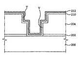
- FIG. 5is a cross sectional view of a metal line of a semiconductor device consistent with another embodiment of the present invention.
- an etch stop layer 202 and an interlayer insulating film 204are formed on a substrate 200 .
- Substrate 200may include individual devices (not shown) or a lower conductor (not shown).
- Etch stop layer 202may be made of SiN, SiH 4 or the like.
- Interlayer insulating film 204may be formed by depositing an organic or inorganic insulating material such as a fluorine silicate glass (FSG), an undoped silicate glass (USG), SiH 4 , and a tetra ethylortho silicate (TEOS) in a single layer or multi layers.
- interlayer insulating layer 204can be formed of a low-k material such as a black diamond (BD) having a dielectric constant not greater than a value of 3.0.
- BDblack diamond
- etch stop layer 202 and interlayer insulating film 204Formed through etch stop layer 202 and interlayer insulating film 204 is a via V for exposing the lower conductor or individual devices therethrough and interlayer insulating film 204 is provided with a trench T through which via V is exposed.
- trench Tformed inside trench T are a barrier layer 214 and a metal line 216 that are connected to the lower conductor and the individual devices electrically.
- Barrier layer 214is formed on an inner surface of trench T and then a via and a trench defined by barrier layer 214 is filled with metal line 216 .
- Barrier layer 214prevents a metal material of metal line 216 from diffusing into another layer such as an insulating film, while enhancing the adhesion of the insulating film and the metal line.
- barrier layer 214is formed of a dual barrier structure comprising a first barrier metal layer 210 and a second barrier metal layer 212 .
- First barrier metal layer 210is formed of TaN
- second barrier metal layer 212is formed of Ta.
- Metal line 216is made of a conductive material such as copper having a low resistance.
- FIGS. 6 to 8provide cross sectional views to describe the method for forming the metal line of the semiconductor fabricating method consistent with an embodiment of the present invention, wherein initial steps of the method are omitted.
- etch stop layer 202 and interlayer insulating film 204are deposited on a substrate 200 .
- interlayer insulating film 204is formed through a selective etching process using a photoresist film (not shown) such that etch stop layer 202 is partially exposed through via V. Thereafter, trench T is formed through a selective etching process using a photoresist film (not shown) such that via V is exposed therethrough. If interlayer insulating film 204 is formed in multiple layers, one of the multi layers of interlayer insulating film 204 can be used as an etch stop layer when trench T is formed.
- the exposed etch stop layer 202is removed to partially expose substrate 200 .
- TaNis deposited by a PVD method to form first barrier metal layer 210 .
- first barrier metal layer 210is converted into Ta by being exposed to and reacting with NO 2 , forming second barrier metal layer 212 , as shown in FIG. 8 . If NO 2 reacts with TaN of first barrier metal layer 210 , N 2 and O 2 are generated and TaN is converted into Ta.
- the Ta film of second barrier metal layer 212is formed in such a manner that its thickness is half of that of the initially formed TaN film.
- a dual TaN/Ta filmis formed by forming a TaN film and converting a part of the TaN film into a Ta film. Specifically, if a dual film is formed thick by a PVD process as the conventional cases, there may occur an overhanging phenomenon. But, since a dual film is formed by using a single film in the present invention, the overhanging phenomenon does not occur.
Landscapes
- Engineering & Computer Science (AREA)
- Physics & Mathematics (AREA)
- Condensed Matter Physics & Semiconductors (AREA)
- General Physics & Mathematics (AREA)
- Manufacturing & Machinery (AREA)
- Computer Hardware Design (AREA)
- Microelectronics & Electronic Packaging (AREA)
- Power Engineering (AREA)
- Internal Circuitry In Semiconductor Integrated Circuit Devices (AREA)
Abstract
Description
Claims (5)
Applications Claiming Priority (2)
| Application Number | Priority Date | Filing Date | Title |
|---|---|---|---|
| KR10-2005-0134359 | 2005-12-29 | ||
| KR1020050134359AKR100738210B1 (en) | 2005-12-29 | 2005-12-29 | Method of forming thin film and metal wiring in semiconductor device |
Publications (2)
| Publication Number | Publication Date |
|---|---|
| US20070161241A1 US20070161241A1 (en) | 2007-07-12 |
| US7439175B2true US7439175B2 (en) | 2008-10-21 |
Family
ID=38214328
Family Applications (1)
| Application Number | Title | Priority Date | Filing Date |
|---|---|---|---|
| US11/645,533ActiveUS7439175B2 (en) | 2005-12-29 | 2006-12-27 | Method for fabricating a thin film and metal line of semiconductor device |
Country Status (3)
| Country | Link |
|---|---|
| US (1) | US7439175B2 (en) |
| KR (1) | KR100738210B1 (en) |
| CN (1) | CN1992176A (en) |
Families Citing this family (1)
| Publication number | Priority date | Publication date | Assignee | Title |
|---|---|---|---|---|
| US7670946B2 (en)* | 2006-05-15 | 2010-03-02 | Chartered Semiconductor Manufacturing, Ltd. | Methods to eliminate contact plug sidewall slit |
Citations (15)
| Publication number | Priority date | Publication date | Assignee | Title |
|---|---|---|---|---|
| US6146993A (en)* | 1998-11-23 | 2000-11-14 | Advanced Micro Devices, Inc. | Method for forming in-situ implanted semiconductor barrier layers |
| US6353260B2 (en)* | 1999-01-04 | 2002-03-05 | Taiwan Semiconductor Manufacturing Company | Effective diffusion barrier |
| US6362526B1 (en)* | 1998-10-08 | 2002-03-26 | Advanced Micro Devices, Inc. | Alloy barrier layers for semiconductors |
| US20020106846A1 (en)* | 2001-02-02 | 2002-08-08 | Applied Materials, Inc. | Formation of a tantalum-nitride layer |
| US20030091739A1 (en)* | 2001-11-14 | 2003-05-15 | Hitoshi Sakamoto | Barrier metal film production apparatus, barrier metal film production method, metal film production method, and metal film production apparatus |
| US20030157794A1 (en)* | 2002-02-20 | 2003-08-21 | International Business Machines Corporation | Edge seal for a semiconductor device |
| US6723635B1 (en)* | 2002-04-04 | 2004-04-20 | Advanced Micro Devices, Inc. | Protection low-k ILD during damascene processing with thin liner |
| US20040175928A1 (en)* | 2002-12-23 | 2004-09-09 | Abell Thomas Joseph | Barrier film integrity on porous low k dielectrics by application of a hydrocarbon plasma treatment |
| US20040253160A1 (en)* | 2003-06-10 | 2004-12-16 | Jones Kenneth Mitchell | Method of neutralizing acid rain |
| US6924207B2 (en)* | 2002-12-26 | 2005-08-02 | Samsung Electronics Co., Ltd. | Method of fabricating a metal-insulator-metal capacitor |
| US6987059B1 (en)* | 2003-08-14 | 2006-01-17 | Lsi Logic Corporation | Method and structure for creating ultra low resistance damascene copper wiring |
| US7229918B2 (en)* | 2005-02-14 | 2007-06-12 | Infineon Technologies Ag | Nitrogen rich barrier layers and methods of fabrication thereof |
| US20070155163A1 (en)* | 2005-12-29 | 2007-07-05 | Dongbu Electronics Co., Ltd. | Method for fabricating a thin film and a metal line of a semiconductor device |
| US20070155169A1 (en)* | 2005-12-29 | 2007-07-05 | In-Cheol Baek | Method of fabricating a thin film and metal wiring in a semiconductor device |
| US7244674B2 (en)* | 2004-04-27 | 2007-07-17 | Agency For Science Technology And Research | Process of forming a composite diffusion barrier in copper/organic low-k damascene technology |
Family Cites Families (3)
| Publication number | Priority date | Publication date | Assignee | Title |
|---|---|---|---|---|
| KR980005370A (en)* | 1996-06-27 | 1998-03-30 | 김주용 | METHOD FOR FORMING METAL WIRING OF SEMICONDUCTOR |
| KR20040009789A (en)* | 2002-07-25 | 2004-01-31 | 아남반도체 주식회사 | Semiconductor device and fabrication method thereof |
| KR100563817B1 (en)* | 2003-12-30 | 2006-03-28 | 동부아남반도체 주식회사 | Copper wiring formation method of semiconductor device |
- 2005
- 2005-12-29KRKR1020050134359Apatent/KR100738210B1/ennot_activeExpired - Fee Related
- 2006
- 2006-12-27CNCNA2006101724326Apatent/CN1992176A/enactivePending
- 2006-12-27USUS11/645,533patent/US7439175B2/enactiveActive
Patent Citations (15)
| Publication number | Priority date | Publication date | Assignee | Title |
|---|---|---|---|---|
| US6362526B1 (en)* | 1998-10-08 | 2002-03-26 | Advanced Micro Devices, Inc. | Alloy barrier layers for semiconductors |
| US6146993A (en)* | 1998-11-23 | 2000-11-14 | Advanced Micro Devices, Inc. | Method for forming in-situ implanted semiconductor barrier layers |
| US6353260B2 (en)* | 1999-01-04 | 2002-03-05 | Taiwan Semiconductor Manufacturing Company | Effective diffusion barrier |
| US20020106846A1 (en)* | 2001-02-02 | 2002-08-08 | Applied Materials, Inc. | Formation of a tantalum-nitride layer |
| US20030091739A1 (en)* | 2001-11-14 | 2003-05-15 | Hitoshi Sakamoto | Barrier metal film production apparatus, barrier metal film production method, metal film production method, and metal film production apparatus |
| US20030157794A1 (en)* | 2002-02-20 | 2003-08-21 | International Business Machines Corporation | Edge seal for a semiconductor device |
| US6723635B1 (en)* | 2002-04-04 | 2004-04-20 | Advanced Micro Devices, Inc. | Protection low-k ILD during damascene processing with thin liner |
| US20040175928A1 (en)* | 2002-12-23 | 2004-09-09 | Abell Thomas Joseph | Barrier film integrity on porous low k dielectrics by application of a hydrocarbon plasma treatment |
| US6924207B2 (en)* | 2002-12-26 | 2005-08-02 | Samsung Electronics Co., Ltd. | Method of fabricating a metal-insulator-metal capacitor |
| US20040253160A1 (en)* | 2003-06-10 | 2004-12-16 | Jones Kenneth Mitchell | Method of neutralizing acid rain |
| US6987059B1 (en)* | 2003-08-14 | 2006-01-17 | Lsi Logic Corporation | Method and structure for creating ultra low resistance damascene copper wiring |
| US7244674B2 (en)* | 2004-04-27 | 2007-07-17 | Agency For Science Technology And Research | Process of forming a composite diffusion barrier in copper/organic low-k damascene technology |
| US7229918B2 (en)* | 2005-02-14 | 2007-06-12 | Infineon Technologies Ag | Nitrogen rich barrier layers and methods of fabrication thereof |
| US20070155163A1 (en)* | 2005-12-29 | 2007-07-05 | Dongbu Electronics Co., Ltd. | Method for fabricating a thin film and a metal line of a semiconductor device |
| US20070155169A1 (en)* | 2005-12-29 | 2007-07-05 | In-Cheol Baek | Method of fabricating a thin film and metal wiring in a semiconductor device |
Also Published As
| Publication number | Publication date |
|---|---|
| KR20070071154A (en) | 2007-07-04 |
| KR100738210B1 (en) | 2007-07-10 |
| CN1992176A (en) | 2007-07-04 |
| US20070161241A1 (en) | 2007-07-12 |
Similar Documents
| Publication | Publication Date | Title |
|---|---|---|
| US8653663B2 (en) | Barrier layer for copper interconnect | |
| US20030139034A1 (en) | Dual damascene structure and method of making same | |
| US8778801B2 (en) | Method for forming seed layer structure | |
| US7679192B2 (en) | Semiconductor device including cover layer | |
| US8338951B2 (en) | Metal line of semiconductor device having a diffusion barrier with an amorphous TaBN layer and method for forming the same | |
| JP4558272B2 (en) | Chrome adhesion layer for copper vias in low dielectric constant technology | |
| US7498262B2 (en) | Method of fabricating a thin film and metal wiring in a semiconductor device | |
| US7531901B2 (en) | Metal interconnection of semiconductor device and method for forming the same | |
| US20070152333A1 (en) | Metal Interconnection of Semiconductor Device and Method of Fabricating the Same | |
| US20090166870A1 (en) | Metal line of semiconductor device and method for forming the same | |
| US7687392B2 (en) | Semiconductor device having metal wiring and method for fabricating the same | |
| US20090001577A1 (en) | Metal line of semiconductor device with a triple layer diffusion barrier and method for forming the same | |
| US7439175B2 (en) | Method for fabricating a thin film and metal line of semiconductor device | |
| US7902065B2 (en) | Multi-layered metal line having an improved diffusion barrier of a semiconductor device and method for forming the same | |
| US7432193B2 (en) | Method for fabricating a thin film and a metal line of a semiconductor device | |
| US20070037378A1 (en) | Method for forming metal pad in semiconductor device | |
| US7777336B2 (en) | Metal line of semiconductor device and method for forming the same | |
| US20070166985A1 (en) | Fabrication Method of Thin Film and Metal Line in Semiconductor Device | |
| KR101098920B1 (en) | Method for manufacturing semicondoctor device | |
| KR100909176B1 (en) | Metal wiring formation method of semiconductor device | |
| KR100588661B1 (en) | Multilayer metal wiring structure and manufacturing method thereof | |
| US7485578B2 (en) | Semiconductor device | |
| US7981781B2 (en) | Metal line of semiconductor device having a diffusion barrier and method for forming the same | |
| US8008708B2 (en) | Metal line of semiconductor device having a diffusion barrier and method for forming the same | |
| KR100784105B1 (en) | Manufacturing Method of Semiconductor Device |
Legal Events
| Date | Code | Title | Description |
|---|---|---|---|
| AS | Assignment | Owner name:DONGBU ELECTRONICS CO., LTD., KOREA, REPUBLIC OF Free format text:ASSIGNMENT OF ASSIGNORS INTEREST;ASSIGNOR:LEE, HAN-CHOON;REEL/FRAME:018745/0045 Effective date:20061130 | |
| STCF | Information on status: patent grant | Free format text:PATENTED CASE | |
| FEPP | Fee payment procedure | Free format text:PAYOR NUMBER ASSIGNED (ORIGINAL EVENT CODE: ASPN); ENTITY STATUS OF PATENT OWNER: LARGE ENTITY | |
| FEPP | Fee payment procedure | Free format text:PAYER NUMBER DE-ASSIGNED (ORIGINAL EVENT CODE: RMPN); ENTITY STATUS OF PATENT OWNER: LARGE ENTITY Free format text:PAYOR NUMBER ASSIGNED (ORIGINAL EVENT CODE: ASPN); ENTITY STATUS OF PATENT OWNER: LARGE ENTITY | |
| FPAY | Fee payment | Year of fee payment:4 | |
| FEPP | Fee payment procedure | Free format text:PAT HOLDER CLAIMS SMALL ENTITY STATUS, ENTITY STATUS SET TO SMALL (ORIGINAL EVENT CODE: LTOS); ENTITY STATUS OF PATENT OWNER: LARGE ENTITY | |
| FEPP | Fee payment procedure | Free format text:PAYER NUMBER DE-ASSIGNED (ORIGINAL EVENT CODE: RMPN); ENTITY STATUS OF PATENT OWNER: LARGE ENTITY Free format text:PAYOR NUMBER ASSIGNED (ORIGINAL EVENT CODE: ASPN); ENTITY STATUS OF PATENT OWNER: LARGE ENTITY | |
| AS | Assignment | Owner name:INPHI CORPORATION, UNITED STATES Free format text:ASSIGNMENT OF ASSIGNORS INTEREST;ASSIGNOR:DONGBU HITEK, CO., LTD.;REEL/FRAME:034009/0157 Effective date:20141008 | |
| AS | Assignment | Owner name:INPHI CORPORATION, CALIFORNIA Free format text:CORRECTIVE ASSIGNMENT TO CORRECT REMOVE PATENT NO. 878209 FROM EXHIBIT B PREVIOUSLY RECORDED AT REEL: 034009 FRAME: 0157. ASSIGNOR(S) HEREBY CONFIRMS THE ASSIGNMENT;ASSIGNOR:DONGBU HITEK, CO., LTD.;REEL/FRAME:034087/0097 Effective date:20141008 | |
| FEPP | Fee payment procedure | Free format text:PAYOR NUMBER ASSIGNED (ORIGINAL EVENT CODE: ASPN); ENTITY STATUS OF PATENT OWNER: LARGE ENTITY Free format text:PAYER NUMBER DE-ASSIGNED (ORIGINAL EVENT CODE: RMPN); ENTITY STATUS OF PATENT OWNER: LARGE ENTITY | |
| FPAY | Fee payment | Year of fee payment:8 | |
| AS | Assignment | Owner name:INPHI CORPORATION, CALIFORNIA Free format text:ASSIGNMENT OF ASSIGNORS INTEREST;ASSIGNOR:DONGBU HITEK, CO., LTD.;REEL/FRAME:041427/0060 Effective date:20141008 | |
| FEPP | Fee payment procedure | Free format text:ENTITY STATUS SET TO UNDISCOUNTED (ORIGINAL EVENT CODE: BIG.) | |
| MAFP | Maintenance fee payment | Free format text:PAYMENT OF MAINTENANCE FEE, 12TH YEAR, LARGE ENTITY (ORIGINAL EVENT CODE: M1553); ENTITY STATUS OF PATENT OWNER: LARGE ENTITY Year of fee payment:12 | |
| AS | Assignment | Owner name:MARVELL TECHNOLOGY CAYMAN I, CAYMAN ISLANDS Free format text:ASSIGNMENT OF ASSIGNORS INTEREST;ASSIGNOR:INPHI CORPORATION;REEL/FRAME:056649/0823 Effective date:20210617 | |
| AS | Assignment | Owner name:CAVIUM INTERNATIONAL, CAYMAN ISLANDS Free format text:ASSIGNMENT OF ASSIGNORS INTEREST;ASSIGNOR:MARVELL TECHNOLOGY CAYMAN I;REEL/FRAME:057279/0519 Effective date:20210620 | |
| AS | Assignment | Owner name:MARVELL ASIA PTE LTD., SINGAPORE Free format text:ASSIGNMENT OF ASSIGNORS INTEREST;ASSIGNOR:CAVIUM INTERNATIONAL;REEL/FRAME:057336/0873 Effective date:20210620 |