US7439120B2 - Method for fabricating stress enhanced MOS circuits - Google Patents
Method for fabricating stress enhanced MOS circuitsDownload PDFInfo
- Publication number
- US7439120B2 US7439120B2US11/464,090US46409006AUS7439120B2US 7439120 B2US7439120 B2US 7439120B2US 46409006 AUS46409006 AUS 46409006AUS 7439120 B2US7439120 B2US 7439120B2
- Authority
- US
- United States
- Prior art keywords
- layer
- polycrystalline silicon
- depositing
- stressed
- silicon gate
- Prior art date
- Legal status (The legal status is an assumption and is not a legal conclusion. Google has not performed a legal analysis and makes no representation as to the accuracy of the status listed.)
- Active, expires
Links
Images


Classifications
- H—ELECTRICITY
- H10—SEMICONDUCTOR DEVICES; ELECTRIC SOLID-STATE DEVICES NOT OTHERWISE PROVIDED FOR
- H10D—INORGANIC ELECTRIC SEMICONDUCTOR DEVICES
- H10D64/00—Electrodes of devices having potential barriers
- H10D64/01—Manufacture or treatment
- H10D64/017—Manufacture or treatment using dummy gates in processes wherein at least parts of the final gates are self-aligned to the dummy gates, i.e. replacement gate processes
- H—ELECTRICITY
- H01—ELECTRIC ELEMENTS
- H01L—SEMICONDUCTOR DEVICES NOT COVERED BY CLASS H10
- H01L21/00—Processes or apparatus adapted for the manufacture or treatment of semiconductor or solid state devices or of parts thereof
- H01L21/02—Manufacture or treatment of semiconductor devices or of parts thereof
- H01L21/04—Manufacture or treatment of semiconductor devices or of parts thereof the devices having potential barriers, e.g. a PN junction, depletion layer or carrier concentration layer
- H01L21/18—Manufacture or treatment of semiconductor devices or of parts thereof the devices having potential barriers, e.g. a PN junction, depletion layer or carrier concentration layer the devices having semiconductor bodies comprising elements of Group IV of the Periodic Table or AIIIBV compounds with or without impurities, e.g. doping materials
- H01L21/28—Manufacture of electrodes on semiconductor bodies using processes or apparatus not provided for in groups H01L21/20 - H01L21/268
- H01L21/28008—Making conductor-insulator-semiconductor electrodes
- H01L21/28017—Making conductor-insulator-semiconductor electrodes the insulator being formed after the semiconductor body, the semiconductor being silicon
- H01L21/28026—Making conductor-insulator-semiconductor electrodes the insulator being formed after the semiconductor body, the semiconductor being silicon characterised by the conductor
- H01L21/28035—Making conductor-insulator-semiconductor electrodes the insulator being formed after the semiconductor body, the semiconductor being silicon characterised by the conductor the final conductor layer next to the insulator being silicon, e.g. polysilicon, with or without impurities
- H01L21/28044—Making conductor-insulator-semiconductor electrodes the insulator being formed after the semiconductor body, the semiconductor being silicon characterised by the conductor the final conductor layer next to the insulator being silicon, e.g. polysilicon, with or without impurities the conductor comprising at least another non-silicon conductive layer
- H01L21/28061—Making conductor-insulator-semiconductor electrodes the insulator being formed after the semiconductor body, the semiconductor being silicon characterised by the conductor the final conductor layer next to the insulator being silicon, e.g. polysilicon, with or without impurities the conductor comprising at least another non-silicon conductive layer the conductor comprising a metal or metal silicide formed by deposition, e.g. sputter deposition, i.e. without a silicidation reaction
- H—ELECTRICITY
- H10—SEMICONDUCTOR DEVICES; ELECTRIC SOLID-STATE DEVICES NOT OTHERWISE PROVIDED FOR
- H10D—INORGANIC ELECTRIC SEMICONDUCTOR DEVICES
- H10D30/00—Field-effect transistors [FET]
- H10D30/01—Manufacture or treatment
- H10D30/021—Manufacture or treatment of FETs having insulated gates [IGFET]
- H10D30/031—Manufacture or treatment of FETs having insulated gates [IGFET] of thin-film transistors [TFT]
- H10D30/0321—Manufacture or treatment of FETs having insulated gates [IGFET] of thin-film transistors [TFT] comprising silicon, e.g. amorphous silicon or polysilicon
- H10D30/0323—Manufacture or treatment of FETs having insulated gates [IGFET] of thin-film transistors [TFT] comprising silicon, e.g. amorphous silicon or polysilicon comprising monocrystalline silicon
- H—ELECTRICITY
- H10—SEMICONDUCTOR DEVICES; ELECTRIC SOLID-STATE DEVICES NOT OTHERWISE PROVIDED FOR
- H10D—INORGANIC ELECTRIC SEMICONDUCTOR DEVICES
- H10D30/00—Field-effect transistors [FET]
- H10D30/60—Insulated-gate field-effect transistors [IGFET]
- H10D30/67—Thin-film transistors [TFT]
- H10D30/674—Thin-film transistors [TFT] characterised by the active materials
- H10D30/6741—Group IV materials, e.g. germanium or silicon carbide
- H10D30/6743—Silicon
- H10D30/6744—Monocrystalline silicon
- H—ELECTRICITY
- H10—SEMICONDUCTOR DEVICES; ELECTRIC SOLID-STATE DEVICES NOT OTHERWISE PROVIDED FOR
- H10D—INORGANIC ELECTRIC SEMICONDUCTOR DEVICES
- H10D30/00—Field-effect transistors [FET]
- H10D30/60—Insulated-gate field-effect transistors [IGFET]
- H10D30/791—Arrangements for exerting mechanical stress on the crystal lattice of the channel regions
- H10D30/794—Arrangements for exerting mechanical stress on the crystal lattice of the channel regions comprising conductive materials, e.g. silicided source, drain or gate electrodes
- H—ELECTRICITY
- H10—SEMICONDUCTOR DEVICES; ELECTRIC SOLID-STATE DEVICES NOT OTHERWISE PROVIDED FOR
- H10D—INORGANIC ELECTRIC SEMICONDUCTOR DEVICES
- H10D64/00—Electrodes of devices having potential barriers
- H10D64/60—Electrodes characterised by their materials
- H10D64/66—Electrodes having a conductor capacitively coupled to a semiconductor by an insulator, e.g. MIS electrodes
- H10D64/661—Electrodes having a conductor capacitively coupled to a semiconductor by an insulator, e.g. MIS electrodes the conductor comprising a layer of silicon contacting the insulator, e.g. polysilicon having vertical doping variation
- H10D64/662—Electrodes having a conductor capacitively coupled to a semiconductor by an insulator, e.g. MIS electrodes the conductor comprising a layer of silicon contacting the insulator, e.g. polysilicon having vertical doping variation the conductor further comprising additional layers, e.g. multiple silicon layers having different crystal structures
- H—ELECTRICITY
- H10—SEMICONDUCTOR DEVICES; ELECTRIC SOLID-STATE DEVICES NOT OTHERWISE PROVIDED FOR
- H10D—INORGANIC ELECTRIC SEMICONDUCTOR DEVICES
- H10D84/00—Integrated devices formed in or on semiconductor substrates that comprise only semiconducting layers, e.g. on Si wafers or on GaAs-on-Si wafers
- H10D84/01—Manufacture or treatment
- H10D84/0123—Integrating together multiple components covered by H10D12/00 or H10D30/00, e.g. integrating multiple IGBTs
- H10D84/0126—Integrating together multiple components covered by H10D12/00 or H10D30/00, e.g. integrating multiple IGBTs the components including insulated gates, e.g. IGFETs
- H10D84/0165—Integrating together multiple components covered by H10D12/00 or H10D30/00, e.g. integrating multiple IGBTs the components including insulated gates, e.g. IGFETs the components including complementary IGFETs, e.g. CMOS devices
- H10D84/0167—Manufacturing their channels
- H—ELECTRICITY
- H10—SEMICONDUCTOR DEVICES; ELECTRIC SOLID-STATE DEVICES NOT OTHERWISE PROVIDED FOR
- H10D—INORGANIC ELECTRIC SEMICONDUCTOR DEVICES
- H10D84/00—Integrated devices formed in or on semiconductor substrates that comprise only semiconducting layers, e.g. on Si wafers or on GaAs-on-Si wafers
- H10D84/01—Manufacture or treatment
- H10D84/02—Manufacture or treatment characterised by using material-based technologies
- H10D84/03—Manufacture or treatment characterised by using material-based technologies using Group IV technology, e.g. silicon technology or silicon-carbide [SiC] technology
- H10D84/038—Manufacture or treatment characterised by using material-based technologies using Group IV technology, e.g. silicon technology or silicon-carbide [SiC] technology using silicon technology, e.g. SiGe
- H—ELECTRICITY
- H10—SEMICONDUCTOR DEVICES; ELECTRIC SOLID-STATE DEVICES NOT OTHERWISE PROVIDED FOR
- H10D—INORGANIC ELECTRIC SEMICONDUCTOR DEVICES
- H10D86/00—Integrated devices formed in or on insulating or conducting substrates, e.g. formed in silicon-on-insulator [SOI] substrates or on stainless steel or glass substrates
- H10D86/01—Manufacture or treatment
Definitions
- the present inventiongenerally relates to stress enhanced MOS circuits and to methods for their fabrication, and more particularly relates to replacement gate fabrication methods and to stress enhanced MOS circuits made by those methods.
- MOSFETmetal oxide semiconductor field effect transistors
- An MOS transistorincludes a gate electrode as a control electrode and spaced apart source and drain regions between which a current can flow. A control voltage applied to the gate electrode controls the flow of current through a channel between the source and drain regions.
- the gain of an MOS transistoris proportional to the mobility ( ⁇ ) of the majority carrier in the transistor channel.
- the current carrying capability and hence the performance of an MOS transistoris proportional to the mobility of the majority carrier in the channel.
- the mobility of holes, the majority carrier in a P-channel MOS (PMOS) transistor, and the mobility of electrons, the majority carrier in an N-channel MOS (NMOS) transistorcan be enhanced by applying an appropriate stress to the channel.
- the known stress engineering methodsgreatly enhance circuit performance by increasing device drive current without increasing device size and device capacitance.
- the stress enhanced MOS circuitcomprises a semiconductor substrate and a gate insulator overlying the semiconductor substrate.
- a gate electrodeoverlies the gate insulator; the gate electrode has side walls and comprises a layer of polycrystalline silicon in contact with the gate insulator and having a first thickness and a layer of electrically conductive stressed material having a second thickness greater than the first thickness overlying the layer of polycrystalline silicon.
- a stress lineroverlies the side walls of the gate electrode.
- the methodcomprises the steps of depositing and patterning a dummy gate material to form a dummy gate electrode and depositing a layer of insulating material overlying the dummy gate electrode. A portion of the layer of insulating material is removed to expose a top portion of the dummy gate electrode and at least a portion of the dummy gate electrode is removed to leave a void. The void is filled with a stressed material to complete a permanent gate electrode.
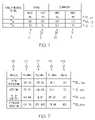
- FIG. 1shows in table form the mobility change resulting from a stress applied to the channel of an MOS transistor in various directions
- FIGS. 2-6illustrate, in cross section, an MOS transistor and methods for its fabrication in accordance with various embodiments of the invention.
- FIG. 7shows stress simulation and mobility enhancement results at various steps in the method in accordance with embodiments of the invention.
- FIG. 1shows the mobility change resulting from a stress of 1 Giga Pascal (GPa) applied to the channel of an MOS transistor in various directions.
- the results shown in the figureapply to an MOS transistor channel formed in a (100) silicon wafer and oriented in a [110] crystal direction.
- Columns 8 and 9relate to the application of a tensile stress applied to the channel of an NMOS transistor and to a PMOS transistor, respectively.
- columns 10 and 11relate to the application of a compressive stress applied to the channel of an NMOS transistor and to a PMOS transistor, respectively.
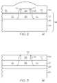
- FIGS. 2-6illustrate a stress enhanced MOS circuit 20 and specifically one exemplary MOS transistor of that circuit and method steps for manufacturing such an MOS circuit in accordance with various embodiments of the invention.
- the exemplary MOS transistoris a stress enhanced N-channel MOS (NMOS) transistor, although similar method steps can be used to manufacture a stress enhanced P-channel MOS (PMOS) transistor as will be explained below.
- CMOScomplementary MOS circuits that use a plurality of stress enhanced NMOS and/or PMOS transistors with or without conventional MOS transistors coupled together to implement a desired integrated circuit.
- MOS deviceproperly refers to a device having a metal gate electrode and an oxide gate insulator, that term will be used throughout to refer to any semiconductor device that includes a conductive gate electrode (whether metal or other conductive material) that is positioned over a gate insulator (whether oxide or other insulator) which, in turn, is positioned over a semiconductor substrate.
- the material selected for the gate electrode of an MOS transistormust have the proper work function to provide the proper threshold voltage of the MOS transistor.
- the gate electrode materialis also selected to have an appropriate stress, compressive for NMOS transistors and tensile for PMOS transistors, and to transfer stress to the channel of the transistor through the gate electrode to enhance the mobility of majority carriers in the channel.
- a gate electrode structurecomprises two layers, a first thin layer to fix the threshold voltage and second thicker layer to transfer stresses into the channel.
- the material of the first layeris chosen based on the work function requirement of the devices.
- the material of the second layeris chosen based on stress, thermal stability, and interface requirements.
- the stress in the second layerideally remains unchanged during the back end processing of the devices.
- the interface between the first layer and second layershould therefore be electrically conducting and chemically stable so that the stresses in the second layer can be effectively transferred to the first layer and then, in turn, to the channel.
- the manufacture of a stress enhanced MOS circuit 20 in accordance with an embodiment of the inventionbegins with providing a P-type semiconductor substrate 22 and forming a stress enhanced MOS transistor in and on that semiconductor substrate.
- the initial steps in the fabrication of MOS circuit 20are conventional and will not be described in detail.
- the semiconductor substrateis preferably a silicon substrate having a (100) surface crystal orientation wherein the term “silicon substrate” is used herein to encompass the relatively pure silicon materials typically used in the semiconductor industry as well as silicon admixed with other elements such as germanium, carbon, and the like.
- the semiconductor substratecan be germanium, gallium arsenide, or other semiconductor material.
- Silicon substrate 22will hereinafter be referred to for convenience but without limitation as a silicon substrate.
- Silicon substrate 22may be a bulk silicon wafer (not illustrated), or may be a thin layer of silicon 24 on an insulating layer 26 (commonly know as silicon-on-insulator or SOI) that, in turn, is supported by a carrier wafer 28 .
- Thin silicon layer 24typically has a thickness of about 20-100 nanometers (nm) depending on the circuit function being implemented, and preferably has a thickness of about 40-60 nm.
- a layer of gate insulator 30is formed on surface 32 of silicon layer 24 .
- the gate insulatormay be thermally grown silicon dioxide formed by heating the silicon substrate in an oxidizing ambient, or may be a deposited insulator such as a silicon oxide, silicon nitride, a high dielectric constant insulator such as HfSiO, or the like. Deposited insulators can be deposited, for example, in known manner by chemical vapor deposition (CVD), low pressure chemical vapor deposition (LPCVD), semi-atmospheric chemical vapor deposition (SACVD), or plasma enhanced chemical vapor deposition (PECVD).
- the gate insulator materialis typically 1-10 nm in thickness.
- a layer of gate electrode forming materialpreferably polycrystalline silicon, is deposited onto the layer of gate insulator.
- gate electrode forming materialssuch as metals and metal silicides may also be deposited providing the material by itself or with appropriate impurity doping can set the necessary threshold voltage of the transistor.
- the gate electrode forming materialwill hereinafter be referred to as polycrystalline silicon although those of skill in the art will recognize that other materials can also be employed.
- the gate electrode forming materialmay also be referred to as a dummy gate material for reasons that will become apparent from the following description. If the gate electrode material is polycrystalline silicon, that material is typically deposited to a thickness of about 50-200 nm and preferably to a thickness of about 100 nm by LPCVD by the hydrogen reduction of silane.
- the layer of polycrystalline siliconis preferably deposited as undoped polycrystalline silicon and is subsequently impurity doped by ion implantation.
- regions of electrically isolating materialsuch as shallow trench isolation (STI) regions can be formed to extend into and preferably entirely through the thickness of silicon layer 24 to electrically isolate between transistors of the MOS circuit as required by the circuit function being implemented.
- STIshallow trench isolation
- the polycrystalline silicon or other gate electrode forming materialis photolithographically patterned and etched to form a dummy or temporary gate electrode 34 .
- Dummy gate electrode 34has substantially the same physical shape and orientation as a permanent gate electrode to be subsequently formed by a replacement process. Although only one MOS transistor is illustrated, in fabricating MOS circuit 20 a plurality of gate electrodes for a plurality of transistors would be patterned from the layer of gate electrode forming material at the same time.
- the pitch between adjacent dummy gate electrodescan be, for example, from about 250 nm to less than 200 nm and preferably less than 150 nm depending on the technology generation.
- Dummy gate electrode 34overlies and defines a channel 36 at the surface of silicon layer 24 .
- the channelis oriented so that current flow along the channel is in the direction.
- the length of the gate electrodedetermines the length of the channel.
- the channel lengthis selected based on the circuit function being implemented.
- the channel lengthis 90 nm or less and most preferably is less than 45 nm.
- Side wall spacers 38are formed on the side walls 40 of dummy gate electrode 34 .
- the sidewall spacerscan be formed of an electrically insulating material such as silicon oxide, silicon nitride, silicon oxynitride, or the like.
- the side wall spacerscan be formed in conventional manner by the deposition and subsequent anisotropic etching of a layer of side wall spacer material. The anisotropic etching can be done, for example, by reactive ion etching (RIE).
- RIEreactive ion etching
- the dummy gate electrode and the side wall spacersare used as a mask and conductivity determining impurities are introduced into near surface regions of silicon layer 24 to form a source region 42 and a drain region 44 .
- the conductivity determining dopantsare introduced into the silicon layer by ion implantation.
- the implanted ionscan be, for example, either phosphorus or arsenic ions.
- the ion implantation or other impurity introducing processcan also be used to impurity dope the polycrystalline silicon dummy gate electrode.
- the side wall spacerscan also be used to form self aligned metal silicide contacts (not illustrated) to the source and drain regions.
- a stress liner 50is blanket deposited to overlie the dummy gate electrode and the side wall spacers.
- the stress lineris formed of an electrically insulating material and can be, for example, a layer of stressed silicon nitride.
- the layer of silicon nitridecan be deposited, for example, by LPCVD or PECVD from reactants including dichlorosilane and ammonia. The deposition conditions, reactants, and reactant flows can be adjusted, as is well known, to deposit either a tensile stress liner or a compressive stress liner.
- a tensile stress lineris deposited overlying an NMOS transistor and a compressive stress liner is deposited overlying a PMOS transistor.
- An additional insulating layer(not illustrated) can also be deposited to add to the thickness of the stress liner and to completely fill the volume between adjacent dummy gate electrodes.
- the method in accordance with one embodiment of the inventioncontinues by exposing a top surface 52 of dummy gate electrode 34 .
- a top portion of dummy gate electrode 34is exposed by a process of chemical mechanical polishing (CMP) of stress liner 50 and any overlying insulating material if such insulating material was deposited over the stress liner.
- CMPchemical mechanical polishing
- exposed top surface 52 of polycrystalline silicon dummy gate electrode 34is etched to reduce the thickness of the polycrystalline silicon as illustrated in FIG. 4 .
- the thickness of the retained polycrystalline silicon 53is reduced to about 10-20 nm or about 10-20% of the original thickness of the dummy gate electrode.
- the remaining thicknessis preferably the minimum thickness that will provide a stable work function and fix the threshold voltage of the device; a thicker retained layer causes the stress transfer from a subsequently deposited overlying layer to the channel to be less efficient.
- the polycrystalline siliconcan be etched, for example, by plasma etching in a Cl or HBr/O 2 chemistry.
- the remaining stress liner 50 and/or insulating layerprovides an etch mask during the etching of the polycrystalline silicon.
- the etchingresults in a void 60 bounded on the sides by side wall spacers 38 and the stress liner.
- Polycrystalline silicon 53 retained at the bottom of the dummy gate electrodeis sufficient to fix the threshold voltage of the MOS transistor.
- the threshold voltageis a function of a number of parameters including the work function of the gate electrode relative to the impurity doping in the transistor channel.
- the work functionis determined, in part, by the impurity doping in the retained polycrystalline silicon.
- the removed portion of polycrystalline silicon dummy gate electrode 34is replaced, for the exemplary NMOS transistor, by depositing a layer of compressive stressed electrically conductive gate electrode material 70 as illustrated in FIG. 5 .
- the compressive stressed gate electrode materialis titanium nitride with a compressive stress of greater than about ⁇ 2.5 GPa and most preferably about ⁇ 10 GPa.
- Compressive stressed titanium nitridecan be deposited by known chemical vapor deposition methods.
- the compressive stressed gate electrode materialis deposited to a thickness sufficient to fill void 60 .
- the excess deposited gate electrode materialis removed from the top surface of the stress liner layer by CMP, selective etching, or the like.
- the resultant structureas illustrated in FIG.
- the 6includes a replacement gate electrode 72 that includes the remaining portion 53 of dummy gate electrode 34 overlaid by a compressive stressed material 70 .
- the compressive stressed materialhas a thickness of at least about 50-80 nm or at least about five times the thickness of the remaining dummy gate electrode material.
- Stress enhanced MOS circuit 20is completed in conventional manner by providing electrical contacts to the source region, drain region, and gate electrode 72 .
- the conventional processingmay include, for example, depositing interlayer dielectrics, etching contact vias, filling the contact vias with conductive plugs, and the like as are well known to those of skill in the art of fabricating semiconductor circuits.
- the replacement gate methodin accordance with the invention, is particularly efficient at maintaining stress in the stressed gate electrode layer and transferring that stress to the channel.
- the stress in most gate electrode forming materials and especially in metallic materialsis relaxed by thermal processing.
- most of the thermal processingsuch as the thermal annealing of the source and drain implants, is completed before the deposition of the stressed gate electrode forming material.
- the back end processing that takes place after the deposition of the stressed material depositionhas a minimal thermal budget.
- a certain amount of confinementis needed around the gate electrode. Such confinement is provided in the inventive method by the side wall spacers and the stress liner layer that are present around the gate electrode region when the stressed gate electrode material is deposited and planarized so the stress transfer to the channel is very effective
- FIG. 7indicates stress simulation results that show the stress evolution and mobility enhancement results during the process of fabricating an NMOS circuit in the manner just described.
- the simulationwas conducted for an N-channel MOS SOI transistor of an MOS circuit formed in and over a ( 100 ) silicon layer having a thickness of 55 nm.
- the channel of the NMOS transistorwas oriented in the direction.
- the gate oxidewas 1 nm in thickness and the gate electrode width was 30 nm with a gate to gate pitch of 130 nm.
- a tensile stress of 1.2 GPawas assumed in the silicon nitride stress liner and a compressive stress of ⁇ 10 GPa was assumed in the titanium nitride replacement gate electrode. Stress was measured in the transistor channel 1 nm below the gate oxide.
- column 120indicates the resulting longitudinal stress along the channel length
- column 122indicates the resulting vertical stress perpendicular to the channel
- column 124indicates the resulting transverse stress in the channel width direction
- column 126indicates the mobility enhancement.
- Column 128indicates the method step completed.
- Row 130indicates the stress and mobility enhancement after deposition of the stress liner
- row 132indicates the stress and mobility enhancement after CMP of the stress liner
- row 134indicates the stress and mobility enhancement after the etch of the dummy gate electrode
- row 136indicates the stress and mobility enhancement after deposition of the compressive stressed replacement gate.
- Each of the stress entriesshows two values for the simulated stress measurement; the first entry is the simulated stress measurement at the gate edge and the second entry is the simulated stress measurement at the center of the channel. For example, for the entry in column 120 and row 136 the simulated stress measurement at the gate edge is a tensile 1.027 GPa, and the simulated stress measurement at the center of the channel is a tensile 1.591 GPa.
- fabricating an MOS circuit in accordance with an embodiment of the inventionresults in a majority carrier electron mobility enhancement of approximately 2.6 times the value of the mobility of a conventional device and approximately 2 times the value of the mobility of a transistor that is conventional except for the use of a stress liner.
- the foregoing descriptionhas provided methods for fabricating an NMOS transistor of a stress enhanced MOS circuit. Similar method steps can be used to fabricate a PMOS transistor with an appropriate change in impurity doping type in the semiconductor substrate and in the source and drain regions. Additionally, the upper portion of the dummy gate electrode must be replaced by a tensile stressed electrically conductive gate electrode material and the stress liner should be compressive stressed. Preferably the tensile stressed electrically conductive gate electrode material has a tensile stress of at least 2.0 GPa.
- One such exampleis the selective growth of embedded silicon germanium in the source and drain regions of a PMOS transistor to increase the compressive longitudinal stress in the channel. Additionally, the stressed replacement gate method in accordance with an embodiment invention can be used either with or without the use of a stress liner.
Landscapes
- Engineering & Computer Science (AREA)
- Chemical & Material Sciences (AREA)
- Chemical Kinetics & Catalysis (AREA)
- Physics & Mathematics (AREA)
- Condensed Matter Physics & Semiconductors (AREA)
- General Physics & Mathematics (AREA)
- Manufacturing & Machinery (AREA)
- Computer Hardware Design (AREA)
- Microelectronics & Electronic Packaging (AREA)
- Power Engineering (AREA)
- Insulated Gate Type Field-Effect Transistor (AREA)
- Metal-Oxide And Bipolar Metal-Oxide Semiconductor Integrated Circuits (AREA)
Abstract
Description
Claims (15)
Priority Applications (2)
| Application Number | Priority Date | Filing Date | Title |
|---|---|---|---|
| US11/464,090US7439120B2 (en) | 2006-08-11 | 2006-08-11 | Method for fabricating stress enhanced MOS circuits |
| US12/208,196US7943999B2 (en) | 2006-08-11 | 2008-09-10 | Stress enhanced MOS circuits |
Applications Claiming Priority (1)
| Application Number | Priority Date | Filing Date | Title |
|---|---|---|---|
| US11/464,090US7439120B2 (en) | 2006-08-11 | 2006-08-11 | Method for fabricating stress enhanced MOS circuits |
Related Child Applications (1)
| Application Number | Title | Priority Date | Filing Date |
|---|---|---|---|
| US12/208,196DivisionUS7943999B2 (en) | 2006-08-11 | 2008-09-10 | Stress enhanced MOS circuits |
Publications (2)
| Publication Number | Publication Date |
|---|---|
| US20080038886A1 US20080038886A1 (en) | 2008-02-14 |
| US7439120B2true US7439120B2 (en) | 2008-10-21 |
Family
ID=39051317
Family Applications (2)
| Application Number | Title | Priority Date | Filing Date |
|---|---|---|---|
| US11/464,090Active2026-10-27US7439120B2 (en) | 2006-08-11 | 2006-08-11 | Method for fabricating stress enhanced MOS circuits |
| US12/208,196Expired - Fee RelatedUS7943999B2 (en) | 2006-08-11 | 2008-09-10 | Stress enhanced MOS circuits |
Family Applications After (1)
| Application Number | Title | Priority Date | Filing Date |
|---|---|---|---|
| US12/208,196Expired - Fee RelatedUS7943999B2 (en) | 2006-08-11 | 2008-09-10 | Stress enhanced MOS circuits |
Country Status (1)
| Country | Link |
|---|---|
| US (2) | US7439120B2 (en) |
Cited By (6)
| Publication number | Priority date | Publication date | Assignee | Title |
|---|---|---|---|---|
| US20080054357A1 (en)* | 2006-08-31 | 2008-03-06 | International Business Machines Corporation | Semiconductor structure with enhanced performance using a simplified dual stress liner configuration |
| US20080102571A1 (en)* | 2006-10-25 | 2008-05-01 | James Pan | Methods for fabricating a stress enhanced mos transistor |
| US20090315114A1 (en)* | 2008-06-23 | 2009-12-24 | Intel Corporation | Stress in trigate devices using complimentary gate fill materials |
| US8183646B2 (en) | 2005-02-23 | 2012-05-22 | Intel Corporation | Field effect transistor with narrow bandgap source and drain regions and method of fabrication |
| US8502351B2 (en) | 2004-10-25 | 2013-08-06 | Intel Corporation | Nonplanar device with thinned lower body portion and method of fabrication |
| US8933458B2 (en) | 2005-06-21 | 2015-01-13 | Intel Corporation | Semiconductor device structures and methods of forming semiconductor structures |
Families Citing this family (7)
| Publication number | Priority date | Publication date | Assignee | Title |
|---|---|---|---|---|
| KR20100047558A (en)* | 2008-10-29 | 2010-05-10 | 삼성전자주식회사 | Semiconductor devices and methods of formign the same |
| US20110042728A1 (en)* | 2009-08-18 | 2011-02-24 | International Business Machines Corporation | Semiconductor device with enhanced stress by gates stress liner |
| JP5452211B2 (en)* | 2009-12-21 | 2014-03-26 | ルネサスエレクトロニクス株式会社 | Semiconductor device and method for manufacturing semiconductor device |
| JP5569243B2 (en) | 2010-08-09 | 2014-08-13 | ソニー株式会社 | Semiconductor device and manufacturing method thereof |
| CN102623405B (en)* | 2011-01-30 | 2014-08-20 | 中国科学院微电子研究所 | Method for forming semiconductor structure |
| US8697523B2 (en)* | 2012-02-06 | 2014-04-15 | International Business Machines Corporation | Integration of SMT in replacement gate FINFET process flow |
| US8962441B2 (en)* | 2013-06-26 | 2015-02-24 | Globalfoundries Inc. | Transistor device with improved source/drain junction architecture and methods of making such a device |
Citations (14)
| Publication number | Priority date | Publication date | Assignee | Title |
|---|---|---|---|---|
| US20050116360A1 (en)* | 2003-12-01 | 2005-06-02 | Chien-Chao Huang | Complementary field-effect transistors and methods of manufacture |
| US20060024879A1 (en) | 2004-07-31 | 2006-02-02 | Taiwan Semiconductor Manufacturing Co., Ltd. | Selectively strained MOSFETs to improve drive current |
| US20060160317A1 (en)* | 2005-01-18 | 2006-07-20 | International Business Machines Corporation | Structure and method to enhance stress in a channel of cmos devices using a thin gate |
| US20060220113A1 (en)* | 2005-03-29 | 2006-10-05 | Fujitsu Limited | P-channel MOS transistor, semiconductor integrated circuit device and fabrication process thereof |
| US20060286729A1 (en) | 2005-06-21 | 2006-12-21 | Jack Kavalieros | Complementary metal oxide semiconductor integrated circuit using raised source drain and replacement metal gate |
| US7164163B2 (en) | 2005-02-22 | 2007-01-16 | Taiwan Semiconductor Manufacturing Company, Ltd. | Strained transistor with hybrid-strain inducing layer |
| US20070045747A1 (en) | 2005-08-26 | 2007-03-01 | Toshiba America Electronic Components, Inc. | Reduction of short-circuiting between contacts at or near a tensile-compressive boundary |
| US20070099414A1 (en)* | 2005-10-31 | 2007-05-03 | Kai Frohberg | Semiconductor device comprising a contact structure based on copper and tungsten |
| US7214629B1 (en) | 2004-11-16 | 2007-05-08 | Xilinx, Inc. | Strain-silicon CMOS with dual-stressed film |
| US20070108526A1 (en) | 2005-11-14 | 2007-05-17 | Toshiba America Electronic Components, Inc. | Strained silicon CMOS devices |
| US20070138570A1 (en)* | 2005-12-16 | 2007-06-21 | Chartered Semiconductor Mfg.LTD | Formation of raised source/drain structures in NFET with embedded SiGe in PFET |
| US7271045B2 (en) | 2005-09-30 | 2007-09-18 | Intel Corporation | Etch stop and hard mask film property matching to enable improved replacement metal gate process |
| US20070246776A1 (en) | 2006-04-20 | 2007-10-25 | Synopsys, Inc. | Stress engineering for cap layer induced stress |
| US20080014704A1 (en)* | 2006-07-13 | 2008-01-17 | Igor Peidous | Field effect transistors and methods for fabricating the same |
Family Cites Families (7)
| Publication number | Priority date | Publication date | Assignee | Title |
|---|---|---|---|---|
| JP4173672B2 (en)* | 2002-03-19 | 2008-10-29 | 株式会社ルネサステクノロジ | Semiconductor device and manufacturing method thereof |
| JP4557508B2 (en)* | 2003-06-16 | 2010-10-06 | パナソニック株式会社 | Semiconductor device |
| US20050214998A1 (en)* | 2004-03-26 | 2005-09-29 | Taiwan Semiconductor Manufacturing Co., Ltd. | Local stress control for CMOS performance enhancement |
| US7288451B2 (en)* | 2005-03-01 | 2007-10-30 | International Business Machines Corporation | Method and structure for forming self-aligned, dual stress liner for CMOS devices |
| US7183613B1 (en)* | 2005-11-15 | 2007-02-27 | International Business Machines Corporation | Method and structure for enhancing both NMOSFET and PMOSFET performance with a stressed film |
| US8384138B2 (en)* | 2006-06-14 | 2013-02-26 | Texas Instruments Incorporated | Defect prevention on SRAM cells that incorporate selective epitaxial regions |
| US7585720B2 (en)* | 2006-07-05 | 2009-09-08 | Toshiba America Electronic Components, Inc. | Dual stress liner device and method |
- 2006
- 2006-08-11USUS11/464,090patent/US7439120B2/enactiveActive
- 2008
- 2008-09-10USUS12/208,196patent/US7943999B2/ennot_activeExpired - Fee Related
Patent Citations (14)
| Publication number | Priority date | Publication date | Assignee | Title |
|---|---|---|---|---|
| US20050116360A1 (en)* | 2003-12-01 | 2005-06-02 | Chien-Chao Huang | Complementary field-effect transistors and methods of manufacture |
| US20060024879A1 (en) | 2004-07-31 | 2006-02-02 | Taiwan Semiconductor Manufacturing Co., Ltd. | Selectively strained MOSFETs to improve drive current |
| US7214629B1 (en) | 2004-11-16 | 2007-05-08 | Xilinx, Inc. | Strain-silicon CMOS with dual-stressed film |
| US20060160317A1 (en)* | 2005-01-18 | 2006-07-20 | International Business Machines Corporation | Structure and method to enhance stress in a channel of cmos devices using a thin gate |
| US7164163B2 (en) | 2005-02-22 | 2007-01-16 | Taiwan Semiconductor Manufacturing Company, Ltd. | Strained transistor with hybrid-strain inducing layer |
| US20060220113A1 (en)* | 2005-03-29 | 2006-10-05 | Fujitsu Limited | P-channel MOS transistor, semiconductor integrated circuit device and fabrication process thereof |
| US20060286729A1 (en) | 2005-06-21 | 2006-12-21 | Jack Kavalieros | Complementary metal oxide semiconductor integrated circuit using raised source drain and replacement metal gate |
| US20070045747A1 (en) | 2005-08-26 | 2007-03-01 | Toshiba America Electronic Components, Inc. | Reduction of short-circuiting between contacts at or near a tensile-compressive boundary |
| US7271045B2 (en) | 2005-09-30 | 2007-09-18 | Intel Corporation | Etch stop and hard mask film property matching to enable improved replacement metal gate process |
| US20070099414A1 (en)* | 2005-10-31 | 2007-05-03 | Kai Frohberg | Semiconductor device comprising a contact structure based on copper and tungsten |
| US20070108526A1 (en) | 2005-11-14 | 2007-05-17 | Toshiba America Electronic Components, Inc. | Strained silicon CMOS devices |
| US20070138570A1 (en)* | 2005-12-16 | 2007-06-21 | Chartered Semiconductor Mfg.LTD | Formation of raised source/drain structures in NFET with embedded SiGe in PFET |
| US20070246776A1 (en) | 2006-04-20 | 2007-10-25 | Synopsys, Inc. | Stress engineering for cap layer induced stress |
| US20080014704A1 (en)* | 2006-07-13 | 2008-01-17 | Igor Peidous | Field effect transistors and methods for fabricating the same |
Cited By (27)
| Publication number | Priority date | Publication date | Assignee | Title |
|---|---|---|---|---|
| US8502351B2 (en) | 2004-10-25 | 2013-08-06 | Intel Corporation | Nonplanar device with thinned lower body portion and method of fabrication |
| US10236356B2 (en) | 2004-10-25 | 2019-03-19 | Intel Corporation | Nonplanar device with thinned lower body portion and method of fabrication |
| US9190518B2 (en) | 2004-10-25 | 2015-11-17 | Intel Corporation | Nonplanar device with thinned lower body portion and method of fabrication |
| US8749026B2 (en) | 2004-10-25 | 2014-06-10 | Intel Corporation | Nonplanar device with thinned lower body portion and method of fabrication |
| US9741809B2 (en) | 2004-10-25 | 2017-08-22 | Intel Corporation | Nonplanar device with thinned lower body portion and method of fabrication |
| US9614083B2 (en) | 2005-02-23 | 2017-04-04 | Intel Corporation | Field effect transistor with narrow bandgap source and drain regions and method of fabrication |
| US9048314B2 (en) | 2005-02-23 | 2015-06-02 | Intel Corporation | Field effect transistor with narrow bandgap source and drain regions and method of fabrication |
| US8368135B2 (en) | 2005-02-23 | 2013-02-05 | Intel Corporation | Field effect transistor with narrow bandgap source and drain regions and method of fabrication |
| US8183646B2 (en) | 2005-02-23 | 2012-05-22 | Intel Corporation | Field effect transistor with narrow bandgap source and drain regions and method of fabrication |
| US8664694B2 (en) | 2005-02-23 | 2014-03-04 | Intel Corporation | Field effect transistor with narrow bandgap source and drain regions and method of fabrication |
| US9368583B2 (en) | 2005-02-23 | 2016-06-14 | Intel Corporation | Field effect transistor with narrow bandgap source and drain regions and method of fabrication |
| US9748391B2 (en) | 2005-02-23 | 2017-08-29 | Intel Corporation | Field effect transistor with narrow bandgap source and drain regions and method of fabrication |
| US8816394B2 (en) | 2005-02-23 | 2014-08-26 | Intel Corporation | Field effect transistor with narrow bandgap source and drain regions and method of fabrication |
| US10121897B2 (en) | 2005-02-23 | 2018-11-06 | Intel Corporation | Field effect transistor with narrow bandgap source and drain regions and method of fabrication |
| US9385180B2 (en) | 2005-06-21 | 2016-07-05 | Intel Corporation | Semiconductor device structures and methods of forming semiconductor structures |
| US8933458B2 (en) | 2005-06-21 | 2015-01-13 | Intel Corporation | Semiconductor device structures and methods of forming semiconductor structures |
| US9761724B2 (en) | 2005-06-21 | 2017-09-12 | Intel Corporation | Semiconductor device structures and methods of forming semiconductor structures |
| US20080054357A1 (en)* | 2006-08-31 | 2008-03-06 | International Business Machines Corporation | Semiconductor structure with enhanced performance using a simplified dual stress liner configuration |
| US7675118B2 (en)* | 2006-08-31 | 2010-03-09 | International Business Machines Corporation | Semiconductor structure with enhanced performance using a simplified dual stress liner configuration |
| US7601574B2 (en)* | 2006-10-25 | 2009-10-13 | Globalfoundries Inc. | Methods for fabricating a stress enhanced MOS transistor |
| US20080102571A1 (en)* | 2006-10-25 | 2008-05-01 | James Pan | Methods for fabricating a stress enhanced mos transistor |
| US9224754B2 (en) | 2008-06-23 | 2015-12-29 | Intel Corporation | Stress in trigate devices using complimentary gate fill materials |
| US8741733B2 (en) | 2008-06-23 | 2014-06-03 | Intel Corporation | Stress in trigate devices using complimentary gate fill materials |
| US9450092B2 (en) | 2008-06-23 | 2016-09-20 | Intel Corporation | Stress in trigate devices using complimentary gate fill materials |
| US8362566B2 (en)* | 2008-06-23 | 2013-01-29 | Intel Corporation | Stress in trigate devices using complimentary gate fill materials |
| US20090315114A1 (en)* | 2008-06-23 | 2009-12-24 | Intel Corporation | Stress in trigate devices using complimentary gate fill materials |
| US9806193B2 (en) | 2008-06-23 | 2017-10-31 | Intel Corporation | Stress in trigate devices using complimentary gate fill materials |
Also Published As
| Publication number | Publication date |
|---|---|
| US20080038886A1 (en) | 2008-02-14 |
| US20090001476A1 (en) | 2009-01-01 |
| US7943999B2 (en) | 2011-05-17 |
Similar Documents
| Publication | Publication Date | Title |
|---|---|---|
| US7439120B2 (en) | Method for fabricating stress enhanced MOS circuits | |
| US7696534B2 (en) | Stressed MOS device | |
| US7442601B2 (en) | Stress enhanced CMOS circuits and methods for their fabrication | |
| US8148214B2 (en) | Stressed field effect transistor and methods for its fabrication | |
| US8159030B2 (en) | Strained MOS device and methods for its fabrication | |
| TWI440097B (en) | Stress-enhanced MOS transistor and method of manufacturing same | |
| US8912606B2 (en) | Integrated circuits having protruding source and drain regions and methods for forming integrated circuits | |
| CN101233605B (en) | Methods for fabricating a stressed MOS device | |
| US7601574B2 (en) | Methods for fabricating a stress enhanced MOS transistor | |
| TWI483315B (en) | Method for manufacturing a stressed MOS device | |
| US7416931B2 (en) | Methods for fabricating a stress enhanced MOS circuit | |
| US7977180B2 (en) | Methods for fabricating stressed MOS devices | |
| US20150235906A1 (en) | Methods for etching dielectric materials in the fabrication of integrated circuits | |
| US20090050963A1 (en) | Stressed mos device and methods for its fabrication | |
| US7462524B1 (en) | Methods for fabricating a stressed MOS device | |
| US8872272B2 (en) | Stress enhanced CMOS circuits and methods for their manufacture |
Legal Events
| Date | Code | Title | Description |
|---|---|---|---|
| AS | Assignment | Owner name:ADVANCED MICRO DEVICES, INC., CALIFORNIA Free format text:ASSIGNMENT OF ASSIGNORS INTEREST;ASSIGNOR:PEI, GEN;REEL/FRAME:018105/0302 Effective date:20060809 | |
| FEPP | Fee payment procedure | Free format text:PAYOR NUMBER ASSIGNED (ORIGINAL EVENT CODE: ASPN); ENTITY STATUS OF PATENT OWNER: LARGE ENTITY | |
| STCF | Information on status: patent grant | Free format text:PATENTED CASE | |
| AS | Assignment | Owner name:GLOBALFOUNDRIES INC., CAYMAN ISLANDS Free format text:AFFIRMATION OF PATENT ASSIGNMENT;ASSIGNOR:ADVANCED MICRO DEVICES, INC.;REEL/FRAME:023119/0083 Effective date:20090630 | |
| FPAY | Fee payment | Year of fee payment:4 | |
| FPAY | Fee payment | Year of fee payment:8 | |
| AS | Assignment | Owner name:WILMINGTON TRUST, NATIONAL ASSOCIATION, DELAWARE Free format text:SECURITY AGREEMENT;ASSIGNOR:GLOBALFOUNDRIES INC.;REEL/FRAME:049490/0001 Effective date:20181127 | |
| MAFP | Maintenance fee payment | Free format text:PAYMENT OF MAINTENANCE FEE, 12TH YEAR, LARGE ENTITY (ORIGINAL EVENT CODE: M1553); ENTITY STATUS OF PATENT OWNER: LARGE ENTITY Year of fee payment:12 | |
| AS | Assignment | Owner name:GLOBALFOUNDRIES U.S. INC., CALIFORNIA Free format text:ASSIGNMENT OF ASSIGNORS INTEREST;ASSIGNOR:GLOBALFOUNDRIES INC.;REEL/FRAME:054633/0001 Effective date:20201022 | |
| AS | Assignment | Owner name:GLOBALFOUNDRIES INC., CAYMAN ISLANDS Free format text:RELEASE BY SECURED PARTY;ASSIGNOR:WILMINGTON TRUST, NATIONAL ASSOCIATION;REEL/FRAME:054636/0001 Effective date:20201117 | |
| AS | Assignment | Owner name:GLOBALFOUNDRIES U.S. INC., NEW YORK Free format text:RELEASE BY SECURED PARTY;ASSIGNOR:WILMINGTON TRUST, NATIONAL ASSOCIATION;REEL/FRAME:056987/0001 Effective date:20201117 |