US7436269B2 - Acoustically coupled resonators and method of making the same - Google Patents
Acoustically coupled resonators and method of making the sameDownload PDFInfo
- Publication number
- US7436269B2 US7436269B2US11/109,596US10959605AUS7436269B2US 7436269 B2US7436269 B2US 7436269B2US 10959605 AUS10959605 AUS 10959605AUS 7436269 B2US7436269 B2US 7436269B2
- Authority
- US
- United States
- Prior art keywords
- resonator
- stage
- filter
- output
- input
- Prior art date
- Legal status (The legal status is an assumption and is not a legal conclusion. Google has not performed a legal analysis and makes no representation as to the accuracy of the status listed.)
- Expired - Lifetime, expires
Links
Images


Classifications
- H—ELECTRICITY
- H03—ELECTRONIC CIRCUITRY
- H03H—IMPEDANCE NETWORKS, e.g. RESONANT CIRCUITS; RESONATORS
- H03H3/00—Apparatus or processes specially adapted for the manufacture of impedance networks, resonating circuits, resonators
- H03H3/007—Apparatus or processes specially adapted for the manufacture of impedance networks, resonating circuits, resonators for the manufacture of electromechanical resonators or networks
- H03H3/02—Apparatus or processes specially adapted for the manufacture of impedance networks, resonating circuits, resonators for the manufacture of electromechanical resonators or networks for the manufacture of piezoelectric or electrostrictive resonators or networks
- H—ELECTRICITY
- H03—ELECTRONIC CIRCUITRY
- H03H—IMPEDANCE NETWORKS, e.g. RESONANT CIRCUITS; RESONATORS
- H03H9/00—Networks comprising electromechanical or electro-acoustic elements; Electromechanical resonators
- H03H9/0023—Networks for transforming balanced signals into unbalanced signals and vice versa, e.g. baluns, or networks having balanced input and output
- H03H9/0095—Networks for transforming balanced signals into unbalanced signals and vice versa, e.g. baluns, or networks having balanced input and output using bulk acoustic wave devices
- H—ELECTRICITY
- H03—ELECTRONIC CIRCUITRY
- H03H—IMPEDANCE NETWORKS, e.g. RESONANT CIRCUITS; RESONATORS
- H03H9/00—Networks comprising electromechanical or electro-acoustic elements; Electromechanical resonators
- H03H9/02—Details
- H03H9/05—Holders or supports
- H03H9/0538—Constructional combinations of supports or holders with electromechanical or other electronic elements
- H03H9/0566—Constructional combinations of supports or holders with electromechanical or other electronic elements for duplexers
- H03H9/0571—Constructional combinations of supports or holders with electromechanical or other electronic elements for duplexers including bulk acoustic wave [BAW] devices
- H—ELECTRICITY
- H03—ELECTRONIC CIRCUITRY
- H03H—IMPEDANCE NETWORKS, e.g. RESONANT CIRCUITS; RESONATORS
- H03H9/00—Networks comprising electromechanical or electro-acoustic elements; Electromechanical resonators
- H03H9/46—Filters
- H03H9/54—Filters comprising resonators of piezoelectric or electrostrictive material
- H03H9/58—Multiple crystal filters
- H03H9/582—Multiple crystal filters implemented with thin-film techniques
- H03H9/583—Multiple crystal filters implemented with thin-film techniques comprising a plurality of piezoelectric layers acoustically coupled
- H03H9/584—Coupled Resonator Filters [CFR]
- H—ELECTRICITY
- H03—ELECTRONIC CIRCUITRY
- H03H—IMPEDANCE NETWORKS, e.g. RESONANT CIRCUITS; RESONATORS
- H03H9/00—Networks comprising electromechanical or electro-acoustic elements; Electromechanical resonators
- H03H9/46—Filters
- H03H9/54—Filters comprising resonators of piezoelectric or electrostrictive material
- H03H9/58—Multiple crystal filters
- H03H9/582—Multiple crystal filters implemented with thin-film techniques
- H03H9/586—Means for mounting to a substrate, i.e. means constituting the material interface confining the waves to a volume
- H03H9/587—Air-gaps
- H—ELECTRICITY
- H03—ELECTRONIC CIRCUITRY
- H03H—IMPEDANCE NETWORKS, e.g. RESONANT CIRCUITS; RESONATORS
- H03H3/00—Apparatus or processes specially adapted for the manufacture of impedance networks, resonating circuits, resonators
- H03H3/007—Apparatus or processes specially adapted for the manufacture of impedance networks, resonating circuits, resonators for the manufacture of electromechanical resonators or networks
- H03H3/02—Apparatus or processes specially adapted for the manufacture of impedance networks, resonating circuits, resonators for the manufacture of electromechanical resonators or networks for the manufacture of piezoelectric or electrostrictive resonators or networks
- H03H3/04—Apparatus or processes specially adapted for the manufacture of impedance networks, resonating circuits, resonators for the manufacture of electromechanical resonators or networks for the manufacture of piezoelectric or electrostrictive resonators or networks for obtaining desired frequency or temperature coefficient
- H03H2003/0414—Resonance frequency
- H03H2003/0421—Modification of the thickness of an element
- H03H2003/0428—Modification of the thickness of an element of an electrode
- H—ELECTRICITY
- H03—ELECTRONIC CIRCUITRY
- H03H—IMPEDANCE NETWORKS, e.g. RESONANT CIRCUITS; RESONATORS
- H03H7/00—Multiple-port networks comprising only passive electrical elements as network components
- H03H7/01—Frequency selective two-port networks
- H03H7/17—Structural details of sub-circuits of frequency selective networks
- H03H7/1708—Comprising bridging elements, i.e. elements in a series path without own reference to ground and spanning branching nodes of another series path
- H—ELECTRICITY
- H03—ELECTRONIC CIRCUITRY
- H03H—IMPEDANCE NETWORKS, e.g. RESONANT CIRCUITS; RESONATORS
- H03H9/00—Networks comprising electromechanical or electro-acoustic elements; Electromechanical resonators
- H03H9/02—Details
- H03H9/02007—Details of bulk acoustic wave devices
- H—ELECTRICITY
- H03—ELECTRONIC CIRCUITRY
- H03H—IMPEDANCE NETWORKS, e.g. RESONANT CIRCUITS; RESONATORS
- H03H9/00—Networks comprising electromechanical or electro-acoustic elements; Electromechanical resonators
- H03H9/70—Multiple-port networks for connecting several sources or loads, working on different frequencies or frequency bands, to a common load or source
- H03H9/703—Networks using bulk acoustic wave devices
- H03H9/706—Duplexers
- Y—GENERAL TAGGING OF NEW TECHNOLOGICAL DEVELOPMENTS; GENERAL TAGGING OF CROSS-SECTIONAL TECHNOLOGIES SPANNING OVER SEVERAL SECTIONS OF THE IPC; TECHNICAL SUBJECTS COVERED BY FORMER USPC CROSS-REFERENCE ART COLLECTIONS [XRACs] AND DIGESTS
- Y10—TECHNICAL SUBJECTS COVERED BY FORMER USPC
- Y10T—TECHNICAL SUBJECTS COVERED BY FORMER US CLASSIFICATION
- Y10T29/00—Metal working
- Y10T29/49—Method of mechanical manufacture
- Y10T29/49002—Electrical device making
Definitions
- the present inventionrelates generally to bulk acoustic wave resonators and filters. More particularly, the present invention relates to acoustically coupled thin-film bulk acoustic resonators (FBARS).
- FBARSacoustically coupled thin-film bulk acoustic resonators
- Thin-film bulk acoustic resonatorsare generally fabricated as a piezoelectric layer sandwiched between two electronically conductive layers that serve as electrodes.
- electrical signalfor example, radio frequency (RF) signal
- RFradio frequency
- Resonance of an FBARoccurs when the wavelength of the mechanical wave generated is approximately twice the thickness of its piezoelectric layer.
- the resonant frequency of an FBARcan range in the order of hundreds of MHz to many tens of GHz.
- FBARSare often used to filter electrical signals at these frequencies.
- multiple FBARSare used to form a band-pass filter where electrical signal having frequency within a predetermined and relatively narrow range (“band”) of frequencies is allowed to pass while electrical signal having frequency outside the band is blocked or redirected to, for example, ground.
- These FBARScan be electrically coupled or acoustically coupled to each other.
- the FBARSare fabricated vertically with a decoupling layer between the FBARS.
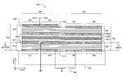
- FIG. 1is a cut-away cross-sectional view of a prior art filter apparatus 100 having two FBAR pairs, each FBAR pair acoustically coupled.
- the filter 100includes a first FBAR 110 , a second FBAR 120 , a third FBAR 130 , and a fourth FBAR 140 .
- the first pairincludes the first FBAR 110 and the second FBAR 120 acoustically coupled to each other.
- the second pairincludes the third FBAR 130 and the fourth FBAR 140 acoustically coupled to each other.
- the first FBAR 110includes a top electrode 112 , a bottom electrode 114 , and a portion of a first piezoelectric layer 116 that is sandwiched between the electrodes 112 and 114 .
- the second FBAR 120includes a portion of a top electrode layer 122 situated under the first FBAR 110 , a portion of a bottom electrode layer 124 situated under the first FBAR 110 , and a portion of a second piezoelectric layer 126 situated under the first FBAR 110 . Lateral boundaries of the second FBAR 120 are defined by the overlaps between the electrode 122 and 124 .
- the first FBAR 110 and the second FBAR 120are acoustically coupled by a decoupling layer 102 .
- the fourth FBAR 140includes a top electrode 142 , a bottom electrode 144 , and a portion of the first piezoelectric layer 116 that is sandwiched between the electrodes 142 and 144 .
- the third FBAR 130includes a portion of the top electrode layer 122 situated under the fourth FBAR 140 , a portion of the bottom electrode layer 124 situated under the fourth FBAR 140 , and a portion of the second piezoelectric layer 126 situated under the fourth FBAR 140 .
- the third FBAR 130 and the fourth FBAR 140are acoustically coupled by the decoupling layer 102 .
- the second FBAR 120 and the third FBARare electrically coupled via the common electrode layer.
- Input electrical signalis injected to the electrodes 112 and 114 exciting the first FBAR 110 thus generating acoustic signal.
- the generated acoustic signalis acoustically coupled to the second FBAR 120 .
- the degree of acoustic couplingis determined by the decoupling layer 102 , typically implemented as multiple sub-layers.
- the second FBAR 120converts the coupled portion of the acoustic signal to electrical signal.
- the electrical signalis electrically coupled to the third FBAR 130 .
- the coupled electrical signalexcites the third FBAR 130 into generating acoustic signal.
- the generated acoustic signalis acoustically coupled to the fourth FBAR 140 .
- the degree of acoustic couplingis determined by the decoupling layer 102 .
- the fourth FBAR 140converts the coupled acoustic signal to electrical signal which is the output electrical signal of the filter 100 .
- the output electrical signalincludes only the desired portions (band) of the input electrical signal while undesired portions are blocked, grounded, or both.
- Such filter apparatuscan be found, for example, in FIG. 3 of U.S. Pat. No. 6,670,866 issued to Ellaet et al. on Dec. 30, 2003 and FIG. 4 of U.S. Pat. No. 6,720,844 issued to Lakin on Apr. 13, 2004.
- the filter apparatus 100is often fabricated over an acoustic mirror 104 , which, in turn, is fabricated above a surface 105 of a substrate 106 .
- the prior art filter apparatus 100suffers from a number of shortcoming.
- the electrodes 112 , 114 , 142 , and 144are relatively distal (vertically 109 in FIG. 1 ) from the top surface 105 of the substrate 106 on which connection pads, for example, a connection pad 108 exists.
- Reliable connections(connecting the electrodes 112 , 114 , 142 , and 144 to such signal traces) are difficult to fabricate due, in part, to the vertical distance 109 such connections are required to span, and sharp corners 107 that such connection would need to include as illustrated by connector 117 .
- an apparatusin a first embodiment, includes a substrate and a two-stage resonator filter fabricated on the substrate.
- the two-stage resonator filterincludes a first stage and a second stage.
- the first stageincludes a first resonator and a second resonator, the second resonator acoustically coupled to the first resonator.
- the second stageincludes a third resonator and a fourth resonator, the fourth resonator acoustically coupled to the third resonator.
- the second resonator and the third resonatorsare electrically coupled.
- a decoupling layercouples the first resonator and the second resonator.
- the decoupling layerextends between the third resonator and the fourth resonator.
- the first resonator and the fourth resonatorare above the substrate.
- the decoupling layeris above the first resonator and the fourth resonator.
- the second resonator and the third resonatorsare above the decoupling layer.
- a method of manufacturing an apparatusis disclosed. First, a cavity is etched within a substrate, the cavity open to a first major surface of the substrate. The cavity is filled with sacrificial material. A two-stage resonator filter is fabricated above the cavity. Then, the sacrificial material is removed from the cavity.
- single-chip duplexerin a third embodiment of the present invention, single-chip duplexer includes a first two-stage resonator filter and a second two-stage resonator filter.
- the first two-stage resonator filteris configured to pass electrical signal having a frequency within a first range of frequencies.
- the first two-stage resonator filterincludes an input resonator, an output resonator, and two floating resonators, each resonator including piezoelectric material.
- the second two-stage resonator filteris configured to pass electrical signal having a frequency within a second range of frequencies.
- the second two-stage resonator filterincludes an input resonator, an output resonator, and two floating resonators, each resonator including piezoelectric material.
- a lower common piezoelectric layeris shared by the first two-stage resonator filter and by the second two-stage resonator filter.
- An upper common piezoelectric layeris shared by the first two-stage resonator filter and by the second first two-stage resonator filter.
- an apparatusin a fourth embodiment of the present invention, includes a two-stage resonator filter connected to two input signal lines and two output signal lines.
- the two-stage resonator filterincludes a first stage including a first resonator and a second resonator, the second resonator acoustically coupled to the first resonator; and a second stage including a third resonator and a fourth resonator, the fourth resonator acoustically coupled to the third resonator.
- the apparatusfurther includes at least one of the following a shunt resonator across the input signal lines; a shunt resonator across the output signal lines; a series resonator along its input signal lines; and a series resonator along its output signal lines.
- an apparatusin a fifth embodiment of the present invention, includes a two-stage resonator filter connected to an input signal line and an output signal line.
- the two-stage resonator filterincludes a first stage including a first resonator and a second resonator; the second resonator acoustically coupled to the first resonator; and a second stage including a third resonator and a fourth resonator, the fourth resonator acoustically coupled to the third resonator.
- a decoupling layeris between the first resonator and the second resonator, the decoupling layer extending between the third resonator and the fourth resonator.
- the apparatusfurther includes a first bridge capacitor bridging the input signal line and the second resonator and a second bridge capacitor bridging the output signal line and the third resonator.
- an apparatusin a sixth embodiment of the present invention, includes a first two-stage resonator filter and a second two-stage resonator filter.
- the first two-stage resonator filteris connected to an input signal line and a first output signal line.
- the first two-stage resonator filterincludes a first stage including a first resonator and a second resonator, the second resonator acoustically coupled to the first resonator; and a second stage including a third resonator and a fourth resonator, the fourth resonator acoustically coupled to the third resonator.
- a decoupling layeris between the first resonator and the second resonator, the decoupling layer extending between the third resonator and the fourth resonator.
- the second two-stage resonator filterincludes a first stage including a first resonator and a second resonator, the second resonator acoustically coupled to the first resonator; and a second stage including a third resonator and a fourth resonator, the fourth resonator acoustically coupled to the third resonator.
- a decoupling layeris between the first resonator and the second resonator, the decoupling layer extending between the third resonator and the fourth resonator. Both the first two-stage resonator and the second two-stage resonator are connected to the same input signal line.
- FIG. 1is a cut-away cross-sectional view of a known two-stage resonator filter
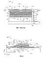
- FIG. 2Ais a top view of a two-stage resonator filter according to a first embodiment of the present invention
- FIG. 2Bis a cut-away cross-sectional view of the two-stage resonator filter of FIG. 2A cut along line 2 B- 2 B;
- FIG. 2Cis a cut-away cross-sectional view of the two-stage resonator filter of FIG. 2A cut along line 2 C- 2 C;
- FIG. 3is a flowchart illustrating a second embodiment of the present invention.
- FIG. 4is a flowchart illustrating a third embodiment of the present invention.
- FIG. 5is a cut-away cross sectional view of a partially fabricated apparatus of FIGS. 2A through 2C
- FIG. 6is a cut-away cross-sectional view of another apparatus illustrating a fourth embodiment of the present invention.
- FIG. 7is a band-pass characteristic curve of the apparatus of FIG. 6 ;
- FIG. 8Ais an apparatus in accordance with fifth embodiment of the present invention.
- FIG. 8Bis a band-pass characteristic curve of the apparatus of FIG. 8A ;
- FIG. 9is an apparatus in accordance with sixth embodiment of the present invention.
- FIG. 10Ais an apparatus in accordance with seventh embodiment of the present invention.
- FIG. 10Bis a band-pass characteristic curve of the apparatus of FIG. 10A ;
- FIG. 11is an apparatus in accordance with eighth embodiment of the present invention.
- FIG. 12is an apparatus in accordance with ninth embodiment of the present invention.
- references to a structure or a portion being formed “on” or “above” another structure or portioncontemplate that additional structures or portions may intervene. References to a structure or a portion being formed on or above another structure or portion without an intervening structure or portion are described herein as being formed “directly on” or “directly above” the other structure or the other portion. Same reference number refers to the same elements throughout this document.
- FIGS. 2A through 2Cillustrate an apparatus 200 including a two-stage resonator filter 204 in accordance with one embodiment of the present invention, two-stage resonator filter 204 fabricated over a cavity 206 within its substrate 202 .
- the two-stage resonator filter 204includes acoustically coupled resonators.
- the cavity 206eliminates the need for the acoustic mirror 104 of the prior art filter 100 of FIG. 1 .
- an input resonator 210 and an output resonator 240are fabricated relatively proximal to the substrate 202 while floating resonators 220 and 230 are fabricated relatively distal to the substrate 202 . Accordingly, necessity of connectors to connection pads (such as the connector 117 of the apparatus 100 of FIG. 1 ) is eliminated or minimized.
- FIG. 2Ais a top view of an apparatus 200 in accordance with one embodiment of the present invention.
- FIG. 2Bis a cutaway side view of the apparatus 200 cut along line 2 B- 2 B.
- FIG. 2Cis a cutaway side view of the apparatus 200 cut along line 2 C- 2 C.
- the apparatus 200includes a substrate 202 and a two-stage resonator filter 204 , for example a double mode two-stage resonator filter (DMF) 204 , fabricated on the substrate 202 .
- DMFdouble mode two-stage resonator filter
- the two-stage resonator filter 204 and each of its component resonatorscan be configured in a wide range of shapes and sizes. Often, the resonator of the two-stage resonator filter 204 has an irregular shape to minimize parasitic resonance and harmonics. Here, for convenience, the two-stage resonator filter 204 is illustrated having generally rectangular shape. Dimension of the two-stage resonator filter 204 and each of its resonators can vary widely depending on application and desired characteristics such as desired frequency band and packaging requirements.
- the two-stage resonator filter 204can have lateral dimensions (in X-Y axes) in the order of hundreds of micrometers and thickness (in Z-axis) in the order of several micrometers or more while each of the resonators of the two-stage resonator filter can have lateral dimensions (in X-Y axes) in the order of hundreds of micrometers and thickness (in Z-axis) in the order of several micrometers.
- the dimensionscan vary widely, even outside these ranges.
- the two-stage resonator filter 204includes a first resonator 210 (also referred to as the input resonator 210 ), a second resonator 220 , a third resonator 230 , and a fourth resonator 240 (also referred to as the output resonator 240 ).
- Each of the resonators ( 210 , 220 , 230 , and 240 )is, in the illustrated embodiment, a thin-film bulk acoustic resonator (FBAR); however, the present embodiment may be implemented using other types of electro-acoustic resonators.
- FBARthin-film bulk acoustic resonator
- Each of the resonators( 210 , 220 , 230 , and 240 ) includes a bottom electrode and a top electrode sandwiching piezoelectric material between the two electrodes.
- the two-stage resonator filter 204is fabricated over a cavity 206 etched within the substrate 202 .
- the apparatus 200includes a first bottom electrode layer 211 fabricated on the substrate 202 . Portions of the first bottom electrode layer 211 overhang the cavity 206 while other portions do not.
- the apparatus 200includes a second bottom electrode layer 241 fabricated on the substrate 202 . Portions of the second bottom electrode layer 241 overhang the cavity 206 while other portions do not.
- the bottom electrode layers 211 and 241include electrically conductive material such as, for example only Molybdenum.
- the bottom electrode layers 211 and 241have thickness (in Z-axis) in the order of tenths of micrometers, for example, 0.21 micrometers. The thickness of the electrode depends on a number of factors such as, for example, frequency and desired characteristics of the two-stage resonator filter 204 . For a DCS (digital cellular system operating frequencies around 1.8 GHz) filter, the typical thickness is about 0.21 micrometer.
- the apparatus 200includes a lower piezoelectric layer 213 fabricated over the first bottom electrode layer 211 and the second bottom electrode layer 241 .
- the apparatus 200includes a first top electrode layer 215 fabricated on the lower piezoelectric layer 213 .
- the piezoelectric layer 213includes piezoelectric material such as, for example only, Aluminum Nitride (AlN).
- the piezoelectric layer 213has thickness (in Z-axis) in the order of micrometers in the illustrated sample embodiment, for example, approximately 1.7 micrometers
- the first resonator 210includes a bottom electrode 212 , a top electrode 216 , and piezoelectric material 214 sandwiched between the bottom electrode 212 and the top electrode 216 .
- the bottom electrode 212is the portion of the bottom electrode layer 211 that overhangs the cavity 206 and also overlaps with the top electrode 216 .
- the top electrode 216is the portion of the first top electrode layer 215 that overhangs the cavity 206 and also overlaps the bottom electrode 212 .
- the piezoelectric material 214is a portion of the lower piezoelectric layer 213 that is between the bottom electrode 212 and the top electrode 216 .
- the apparatus 200includes a second top electrode layer 245 fabricated on the lower piezoelectric layer 213 .
- the fourth resonator 240includes a bottom electrode 242 , a top electrode 246 , and piezoelectric material 244 sandwiched between the bottom electrode 242 and the top electrode 246 .
- the bottom electrode 242is the portion of the bottom electrode layer 241 that overhangs the cavity 206 and also overlaps the top electrode 246 .
- the top electrode 246is the portion of the second electrode layer 245 that overhangs the cavity 206 and also overlaps the bottom electrode 242 .
- the piezoelectric material 244is a portion of the lower piezoelectric layer 213 that is between the bottom electrode 242 and the top electrode 246 .
- the apparatus 200includes a decoupling layer 250 fabricated over the top electrode layers 215 and 245 .
- the decoupling layer 250is provided between the first resonator 210 and the second resonator 220 .
- the decoupling layer 250extending between the third resonator 230 and the fourth resonator 240 as illustrated in FIGS. 2A through 2C and further discussed below.
- the decoupling layer 250is illustrated including sub-layers 250 a , 250 b , and 250 c.
- the decoupling layer 250can be a single layer or can consist of mirrors, each mirror including two layers (a pair of) of materials with different acoustical impedance. If the decoupling layer 250 is implemented including mirrors, then the decoupling layer 250 is often implemented using an odd number of layers such that the decoupling layer 250 is symmetrical to resonators to either side of the decoupling layer 250 .
- the decoupling layer 250can be have the following structures: a low-impedance layer (L) 250 a —high-impedance layer (H) 250 b —low-impedance layer (L) 250 c (LHL); LHLHL; etc.
- each sub-layer in the mirror of the decoupling layer 250in the illustrated embodiment, is approximately one quarter of wavelength of the desired acoustic signal to be coupled by the decoupling layer 250 .
- the thicknesscan vary depending on a number of factors and desired characteristics such as, for example, the material of the mirrors, the number of mirrors, desired coupling strength, etc.
- Acoustic coupling efficiencythe degree of coupling of acoustic signal, from the first resonator 210 to the second resonator 220 depends on a number of factors, for example, material properties of each layer of the decoupling layer 250 ; number of mirrors in the decoupling layer 250 ; thickness of each layer of the decoupling layer 250 .
- Materials for the mirror pairscan include, for example only, the following material pairs:
- a simple coupling structurecan be three layers such as SiO2/W/SiO2 if the impedance difference between the low and high impedance material is large. When such simple structure is used, the thickness of each layer needs to be adjusted for required bandwidth of the filter designed. Some typical numbers for a WCDMA filter application, the coupling structure could have, in the illustrated embodiment, thicknesses of SiO2 sub-layer (4800 Angstroms), W sub-layer (5200 Angstroms), and SiO2 sub-layer (4800 Angstroms).
- SiO2is a desirable material in the decoupling layer 250 because of its properties such as, for example, low acoustical impedance, commonly available in integrated circuit (IC) fabrication process, comprehensive stress (useful for compensating tensile stress associated with most of materials with high acoustical impedance), and positive temperature coefficient (useful for compensating negative temperature coefficient of FBAR resonators).
- SiO2is often used as temporary sacrificial material during the fabrication of the cavity 206 . That is, during the fabrication process, SiO2 is used to first fill the cavity, then the filler SiO2 is removed using hydrofluoric acid bath. It would be undesirable for the SiO2 layers of the decoupling layer 250 during the step to remove the SiO2 in the cavity. This problem is overcome in various method discussed herein below.
- the apparatus 200includes a third bottom electrode layer 221 fabricated over the decoupling layer 250 , an upper piezoelectric layer 223 fabricated over the third bottom electrode layer 221 , and a third top electrode layer 225 fabricated over the upper piezoelectric layer 223 .
- the third bottom electrode layer 221is hidden behind other portions and is illustrated using dashed line in FIG. 2A .
- the second resonator 220includes a bottom electrode 222 , a top electrode 226 , piezoelectric material 224 sandwiched between the bottom electrode 222 and the top electrode 226 .
- the bottom electrode 222is the portion of the bottom electrode layer 221 that is situated over the first resonator 210 and overlaps the top electrode 226 .
- the top electrode 226is the portion of the top electrode layer 225 that is situated over the first resonator 210 and overlaps the bottom electrode 222 .
- the piezoelectric material 224is a portion of the upper piezoelectric layer 223 that is between the bottom electrode 222 and the top electrode 226 .
- the lateral dimensions of the second resonator 220are determined by the overlaps between bottom electrode 222 and top electrode 226 .
- the third resonator 230includes a bottom electrode 232 , a top electrode 236 , piezoelectric material 234 sandwiched between the bottom electrode 232 and the top electrode 236 .
- the bottom electrode 232is the portion of the bottom electrode layer 221 that is situated over the fourth resonator 240 and overlaps the top electrode 236 .
- the top electrode 236is the portion of the top electrode layer 225 that is situated over the fourth resonator 240 and overlaps the bottom electrode 232 .
- the piezoelectric material 234is a portion of the upper piezoelectric layer 223 that is between the bottom electrode 232 and the top electrode 236 . (The lateral dimensions of the third resonator 230 are determined by the overlaps between bottom electrode 232 and top electrode 236 .
- the first resonator 210 and the second resonator 220are acoustically coupled via a portion of the decoupling layer 250 .
- the first resonator 210 and the second resonator 220make up a first stage of the two-stage resonator filter 204 .
- the third resonator 230 and the fourth resonator 240are acoustically coupled via another portion of the decoupling layer 250 .
- the third resonator 230 and the fourth resonator 240make up a second stage of the two-stage resonator filter 204 .
- the second resonator 220 and the third resonator 230are electrically coupled. This is because the bottom electrode 222 of the second resonator 220 and the bottom electrode 232 of the third resonator 230 are portions of the same third electrode layer 221 . Further, this is also because the top electrode 226 of the second resonator 220 and the top electrode 236 of the third resonator 230 are portions of the same third top electrode layer 225 .
- Each of the four resonators 210 , 220 , 230 , and 240 making up the two-stage resonator filter 204can be configured in a wide range of shapes and sizes. Often, these resonators have irregular shapes to minimize parasitic resonance and harmonics. Here, for convenience, each of these resonators is illustrated having a generally rectangular shape. Dimension of these resonators can vary widely depending on application and desired characteristics as already discussed above with sample dimensions.
- a portion 217 of the first bottom electrode layer 211is left exposed (that is, not covered by subsequently fabricated layers) to serve as a connection pad 217 for input signal.
- a portion 247 of the second bottom electrode layer 241is left exposed (that is, not covered by subsequently fabricated layers) to serve as a connection pad 247 for output signal.
- a portion 219 of the first top electrode layer 215is left exposed (that is, not covered by subsequently fabricated layers) to serve as a connection pad 219 for input signal.
- a portion 249 of the second top electrode layer 245is left exposed (that is, not covered by subsequently fabricated layers) to serve as a connection pad 249 for output signal.
- input electrical signalis applied to input connection pads 217 and 219 , and output electrical signal is extracted via the output connection pads 247 and 249 .
- the first resonator 210is also referred to as the input resonator.
- the fourth resonator 240is also referred to as the output resonator.
- the second resonator 220 and the third resonator 230are said to “float” above the first resonator 210 and the fourth resonator 240 .
- the second resonator 220 and the third resonator 230are also referred to as floating resonators.
- Input electrical signalis injected to the electrodes 212 and 216 exciting the input resonator 210 causing input resonator 210 to vibrate thus generating acoustic signal.
- the generated acoustic signalis acoustically coupled to the second resonator 220 .
- the degree of acoustic couplingis determined by the decoupling layer 250 as discussed above.
- the second resonator 220converts the coupled portion of the acoustic signal to electrical signal.
- the electrical signalis electrically coupled to the third resonator 230 with which the second resonator shares the third bottom electrode layer 221 and the third top electrode layer 225 .
- the coupled electrical signalexcites the third resonator 230 into generating acoustic signal.
- the generated acoustic signalis acoustically coupled to the fourth resonator 240 .
- the degree of acoustic couplingis determined by the decoupling layer 250 .
- the fourth resonator 240converts the coupled acoustic signal to electrical signal which is the output electrical signal of the two-stage resonator filter 204 .
- the output electrical signalincludes only the desired portions (band) of the input electrical signal while undesired portions are routed to ground (connection not illustrated in the Figures).
- the cavity 206provides for separation of the two-stage resonator filter 204 from the substrate 202 thereby allowing the two-stage resonator filter 204 to vibrate freely.
- the cavity 206can be configured in a wide range of shapes and sizes. For convenience, the cavity 206 is illustrated having a generally rectangular shape. Dimension of the cavity 206 can vary widely depending on application and desired characteristics. For example, in the illustrated embodiment, the cavity 206 has lateral dimensions (in X-Y axes) in the order of hundreds of micrometers and depth (in Z-axis) in the order of several micrometers or more.
- the apparatus 200 of the present inventiondoes not require the acoustic mirror 104 (as used by the apparatus 100 of FIG. 1 ). For this reason, the two-stage resonator filter 204 is fabricated directly on the substrate 202 . Further, here, input resonator 210 and the output resonator 240 are fabricated relatively proximal to the substrate 202 while floating resonators 220 and 230 are fabricated relatively distal to the substrate 202 . Accordingly, necessity of connectors to connection pads (such as the connector 117 of the apparatus 100 of FIG. 1 ) is eliminated or minimized.
- FIG. 3is a flowchart 300 illustrating a method of fabricating an apparatus according to another embodiment of the present invention.
- the apparatus fabricatedbeing an apparatus such as, for example, the apparatus 200 of FIGS. 2A through 2C .
- the cavity 206is etched.
- the cavity 206is open to a first major surface 203 of the substrate 202 .
- Step 302The cavity is filled with some sacrificial material such as, for example only, SiO2, Aluminum (Al), Germanium (Ge), amorphous Silicon (amorphous-Si), porous Silicon (porous-Si), or phosphorus silicate glass (PSG).
- PSGphosphorus silicate glass
- the two-stage resonator filter 204is fabricated over the cavity leaving an access gap 207 for evacuation of the sacrificial material.
- Step 306To fabricated each layer of the two-stage resonator filter 204 , known deposit and etch techniques can be used.
- the sacrificial materialis removed from the cavity 206 thereby clearing the cavity 206 .
- Step 308This step is often performed by introducing the apparatus 200 into an acid bath.
- the decoupling layer 250can be protected (during the step 308 to remove the sacrificial material) by other layers of the two-stage resonator filter 204 .
- One embodiment of this techniqueis illustrated in FIGS. 2A through 2C where the lower piezoelectric layer 213 and the upper piezoelectric layer 223 envelope and enclose the decoupling layer 250 thereby protecting the decoupling layer 250 from the acid bath which removes the sacrificial material from the cavity 206 .
- the decoupling layer 250need not be enveloped or protected by other layers.
- piezoelectric layerscan be used to protect the decoupling layer 250 from damage during the step 308 of clearing the cavity 206 should the decoupling layer 250 include same or similar material as the sacrificial material used for the cavity 206 .
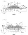
- FIG. 5illustrates a cut-away side view of the apparatus 200 a .
- the apparatus 200 ahas similar structure as the apparatus 200 of FIGS. 2A through 2C .
- portions of the apparatus 200 a of FIG. 5are similar to corresponding portions of the apparatus 200 of FIGS. 2A through 2C .
- portions in FIG. 5 that are similar to corresponding portions in FIGS. 2A through 2Care assigned the same reference numerals, analogous but changed portions are assigned the same reference numerals accompanied by letter “a.”
- the cavity 206is etched. Step 322 .
- the cavity 206is open to a first major surface 203 of the substrate 202 .
- the cavityis filled with some sacrificial material such as, for example only, SiO2, Aluminum (Al), Germanium (Ge), amorphous Silicon (amorphous-Si), porous Silicon (porous-Si), or phosphorus silicate glass (PSG).
- SiO2silicon
- AlAluminum
- GeGermanium
- amorphous Siliconamorphous-Si
- porous Siliconporous Silicon
- PSGphosphorus silicate glass
- the first resonator 210 and a fourth resonatorare fabricated in the same manner as the first resonator 210 and the fourth resonator 240 of the apparatus 200 of FIGS. 2A through 2C .
- Step 326The sacrificial material is removed from the cavity 206 thereby clearing the cavity 206 .
- Step 328Then, the access gap 207 is plugged whereby access to the cavity 206 is closed.
- a plug 208can be fabricated using dielectric materials such as polyamide which is spun on and patterned with photolithograph process.
- Step 232the rest of the elements of the apparatus 200 a are fabricated including the decoupling layer 250 and upper resonators (the second resonator 220 and the third resonator hidden behind the illustrated portions in FIG. 5 ).
- Step 232To fabricated the rest of the elements of the two-stage resonator filter 204 , known deposit and etch techniques can be used.
- the decoupling layer 250need not be exposed to the chemicals used to clear the cavity 206 .
- same or similar materialscan be used for the decoupling layer 250 and as the sacrificial material.
- the upper piezoelectric layer 223 a hereneed not envelope the decoupling layer 250 .
- FIG. 6another embodiment of the present invention is illustrated in FIG. 6 as a single-chip duplexer 400 including a substrate 402 and a first two-stage resonator filter 404 and a second two-stage resonator filter 454 on the substrate 402 .
- the first two-stage resonator filter 404 and the second two-stage resonator filter 454have similar structure as and operates under similar principles to the two-stage resonator filter 204 of FIGS. 2A through 2C .
- the first two-stage resonator filter 404includes its input resonator 410 and output resonator 440 relatively proximal to the substrate 402 .
- a decoupling layer 450is above the input resonator 410 and the output resonator 440 .
- floating resonators(a second resonator 420 and a third resonator 430 ) are above the decoupling layer 450 .
- Each of these resonators 410 , 420 , 430 , and 440include piezoelectric material as illustrated.
- the second two-stage resonator filter 454includes its input resonator 460 and output resonator 490 relatively proximal to the substrate 402 .
- the decoupling layer 450is above the input resonator 460 and the output resonator 490 .
- floating resonators(a second resonator 470 and a third resonator 480 ) are above the decoupling layer 450 .
- Each of these resonators 460 , 470 , 480 , and 490include piezoelectric material as illustrated.
- the single-chip duplexer 400includes two two-stage resonator filters 404 and 454 on the same chip, the first two-stage resonator filter 404 and the second two-stage resonator filter 454 share a lower common piezoelectric layer 413 and share an upper common piezoelectric layer 423 . That is, different portions of the contiguous lower common piezoelectric layer 413 are used within the first two-stage resonator filter 404 to constitute its resonators and are used within the second two-stage resonator filter 454 to constitute its resonators.
- first two-stage resonator filter 404 and the second two-stage resonator filter 454share the decoupling layer 450 . That is, different portions of the decoupling layer 450 are used within the first two-stage resonator filter 404 and are used within the second two-stage resonator filter 454 .
- two-stage resonator filtersare often implemented as a band-pass filter where electrical signal having frequency within a predetermined and relatively narrow range (“band”) of frequencies is allowed to pass while electrical signal having frequency outside the band is blocked.
- bandrelatively narrow range
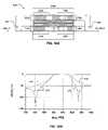
- FIG. 7illustrates the band-pass characteristics of the single-chip duplexer 400 .
- the first two-stage resonator filter 404is configured to pass electrical signal having a frequency within a first pass band range 409 of frequencies (as illustrated by first band-pass characteristic curve 405 ) while the second two-stage resonator filter 454 is configured to pass electrical signal having a frequency within a second pass band range 459 of frequencies (as illustrated by second band-pass characteristic curve 455 ).
- the band-pass characteristic curves 405 and 455 and similar graph curvesare often referred to as pass band curves because they illustrate bands of frequencies passed by the two-stage resonator filters 404 and 454 .
- Input and output signals of the single-chip duplexer 400are further processed by other circuits such as, for example only, a phase shifter 406 .
- the phase shifter 406can be used to isolate the two-stage resonator filters 404 and 454 from each other to reduce influence of one of the two-stage resonator filters 404 and 454 on the other two-stage resonator filter as the single-chip duplexer 400 operates with external circuits such as, for example, an antenna.
- the difference in the band-pass ranges 409 and 459is achieved by mass loading the resonators of the first two-stage resonator filter 404 such that the resonators of the first two-stage resonator filter 404 has a different resonant frequency compared to the resonators of the second two-stage resonator filter 454 .
- massis added to top electrodes 416 and 426 of the resonators of the first two-stage resonator filter 404 increasing the thickness (in the Z-axis) of the resonators thereby increasing the wavelength of the resonant frequency of these resonators. Increased resonant wavelength translates into lower resonant frequency.
- the two-stage resonator filter 204 illustrated in FIGS. 2A through 2Chas band-pass characteristic having similar shape as the band-pass characteristic curves 405 and 455 in FIG. 7 .
- Band-pass characteristics having different characteristics, for example, sharper roll-offcan be achieved using the two-stage resonator filter 204 in combination of other circuit elements.
- FIG. 8Aillustrates a filter apparatus 500 including a two-stage resonator filter 204 with a first shunt thin-film baulk acoustic resonator (FBAR) 502 in the input side of the two-stage resonator filter 204 and a second shunt thin-film baulk acoustic resonator (FBAR) 504 in the output side of the two-stage resonator filter 204 .
- the filter apparatus 500with the shunt resonators 502 and 504 , has band-pass characteristic as illustrated by band-pass characteristic curve 506 of FIG.
- the shunt resonators 502 and 504are tuned to near 1.79 GHz, at the lower end 510 of the band-pass range 508 compared to, for example, at the upper end 512 of the band-pass range 508 .
- the upper end 512 of the band-pass range 508has relatively gradual roll-off.
- serial resonatorscan be added to the input and output lines. This is illustrated as a filter apparatus 520 of FIG. 9 .
- the filter apparatus 520 of FIG. 9includes portions similar to corresponding portions of filter apparatus 500 of FIG. 8A . Portions of filter apparatus 520 of FIG. 9 that are similar to corresponding portions of filter apparatus 500 of FIG. 8A are assigned the same reference numerals.
- the filter apparatus 520includes all the portions of the filter apparatus 500 of FIG. 8A .
- the filter apparatus 520includes series resonators, for example FBARs, 522 and 524 in its input lines and series resonators, for example FBARs, 526 and 528 in its output lines.
- the series resonators 522 , 524 , 526 , and 528are tuned to tuned to near 1.89 GHz, at the upper end 512 of the band-pass range 508 resulting in a sharper roll-off of the band-pass characteristic curve 506 at the at the upper end 512 of the band-pass range 508 .
- the sharper roll-offis not illustrated.
- FIG. 10Aillustrates an alternative technique for adjusting the band-pass characteristics of a two-stage resonator filter.
- a filter apparatus 530includes a two-stage resonator filter 204 b that is similar to the two-stage resonator filter 204 of FIGS. 2A through 2C but tuned to have a band-pass frequency range ranging from approximately 820 MHz to 850 MHz as illustrated by band-pass characteristic curve 532 of FIG. 10B .
- the two-stage resonator filter 204 bhas similar structure as the two-stage resonator filter 204 of FIGS. 2A through 2C . Further, portions of the two-stage resonator filter 204 b of FIG.
- FIGS. 10Aare similar to corresponding portions of the two-stage resonator filter 204 b of FIGS. 2A through 2C .
- portions in FIG. 10A that are similar to corresponding portions in FIGS. 2A through 2Care assigned the same reference numerals, analogous but changed portions are assigned the same reference numerals accompanied by letter “b.”
- the filter apparatus 530includes bridge capacitors 534 and 536 .
- the input signal lineis connected to the bottom electrode of the first resonator 210 b and the output signal line is connected to the bottom electrode of the fourth resonator 240 b .
- the top electrodes of the first resonator 210 b and the fourth resonator 240 bare grounded as well as the bottom electrodes of the floating resonators 220 b and 230 b.
- the first bridge capacitor 534connects the input signal line with the top electrode of the second resonator 220 b of the first coupled-resonator pair ( 210 b and 220 b ).
- the second bridge capacitor 536connects the output signal line with the top electrode of the third resonator 230 b of the second coupled-resonator pair ( 230 b and 240 b ).
- These bridge capacitors 534 and 536are connected to the electrodes with opposite phase in the coupled-resonator pairs.
- the bridge capacitors 534 and 536provide a connection for electrical current which has opposite phase compared to current generated by acoustic coupling at the desired frequency. That is electrical current through the capacitors 534 and 536 has oppose phase compared to the phase of the electrical current induced by acoustic coupling.
- the bridge capacitors 534 and 536have values in the order of tenths of pico-Farads or less, for example 0.5 pico-Farads or less.
- FIG. 11illustrates a filter apparatus 530 c that is an alternative embodiment of the filter apparatus 530 of FIG. 10A .
- the filter apparatus 530 chas similar components as the filter apparatus 530 but the components are connected differently to achieve the same effect.
- the input signal lineis connected to the top electrode of the first resonator 210 b and the output signal line is connected to the top electrode of the fourth resonator 240 b .
- the bottom electrodes of the first resonator 210 b and the fourth resonator 240 bare grounded as well as the top electrodes of the floating resonators 220 b and 230 b .
- the first bridge capacitor 534connects the input signal line with the bottom electrode of the second resonator 220 b of the first coupled-resonator pair ( 210 b and 220 b ).
- the second bridge capacitor 536connects the output signal line with the bottom electrode of the third resonator 230 b of the second coupled-resonator pair ( 230 b and 240 b ).
- the roll-off effect realizedis the same as the roll-off effect illustrated in FIG. 10B and discussed above.
- FIG. 12illustrates a filter apparatus 570 illustrating yet another application of the two-stage resonator filter of the present invention.
- the filter apparatus 570includes a first two-stage resonator filter 204 c and a second two-stage resonator filter 204 d connected in parallel to provide a singled ended input to balanced output.
- Each of the two-stage resonator filters 204 c and 204 dhas similar configuration as the two-stage resonator filters 204 of FIGS. 2A through 2C .
- Each of the two-stage resonator filters 204 c and 204 dprovides 100 ohms of input and output impedance.
- the two-stage resonator filters 204 c and 204 dcombined in parallel, provide a 50 ohm single input impedance line and a differential output lines of 100 ohms impedance each for a total combined 200 ohm impedance output.
- These output lines OUTPUT 1 and OUTPUT 2can be fed into an amplifier that usually require 200 ohm impedance matching differential input thereby providing a 1-4 input-to-output impedance transformation.
- These impedance valuesare for example only, and other values of impedance transformation can be realized.
- the input signal lineis connected to the top electrode of the first resonator 210 c of the first two-stage resonator filter 204 c while connected to the bottom electrode of the first resonator 210 d of the second two-stage resonator filter 204 d .
- the first output signal line OUTPUT 1is connected to the bottom electrode of the fourth resonator 240 c of the first two-stage resonator filter 204 c and the second output signal line OUTPUT 2 is connected to the bottom electrode of the fourth resonator 240 d of the second two-stage resonator filter 204 d .
- the output signals at OUTPUT 1 and the OUTPUT 2form a balanced output.
Landscapes
- Physics & Mathematics (AREA)
- Acoustics & Sound (AREA)
- Chemical & Material Sciences (AREA)
- Crystallography & Structural Chemistry (AREA)
- Engineering & Computer Science (AREA)
- Manufacturing & Machinery (AREA)
- Piezo-Electric Or Mechanical Vibrators, Or Delay Or Filter Circuits (AREA)
Abstract
Description
- Silicon Dioxide (SiO2) and Tungsten (W);
- SiO2 and Molybdenum (Mo);
- SiO2 and Aluminum Nitride (AlN);
- Si3N4 (silicon nitride) and Mo;
- Si3N4 and W;
- amorphous Silicon (Si) and Mo;
- amorphous Si and W;
- AlN and W; or
- AlN and Mo.
Claims (6)
Priority Applications (4)
| Application Number | Priority Date | Filing Date | Title |
|---|---|---|---|
| US11/109,596US7436269B2 (en) | 2005-04-18 | 2005-04-18 | Acoustically coupled resonators and method of making the same |
| GB0604892AGB2425417B (en) | 2005-04-18 | 2006-03-10 | Acoustically coupled resonators and method of making the same |
| US12/207,304US20090096547A1 (en) | 2005-04-18 | 2008-09-09 | Acoustically coupled resonators and method of making the same |
| GB0907292AGB2457607B (en) | 2005-04-18 | 2009-04-28 | Acoustically coupled resonators and method of making the same |
Applications Claiming Priority (1)
| Application Number | Priority Date | Filing Date | Title |
|---|---|---|---|
| US11/109,596US7436269B2 (en) | 2005-04-18 | 2005-04-18 | Acoustically coupled resonators and method of making the same |
Related Child Applications (1)
| Application Number | Title | Priority Date | Filing Date |
|---|---|---|---|
| US12/207,304DivisionUS20090096547A1 (en) | 2005-04-18 | 2008-09-09 | Acoustically coupled resonators and method of making the same |
Publications (2)
| Publication Number | Publication Date |
|---|---|
| US20060232361A1 US20060232361A1 (en) | 2006-10-19 |
| US7436269B2true US7436269B2 (en) | 2008-10-14 |
Family
ID=36241403
Family Applications (2)
| Application Number | Title | Priority Date | Filing Date |
|---|---|---|---|
| US11/109,596Expired - LifetimeUS7436269B2 (en) | 2005-04-18 | 2005-04-18 | Acoustically coupled resonators and method of making the same |
| US12/207,304AbandonedUS20090096547A1 (en) | 2005-04-18 | 2008-09-09 | Acoustically coupled resonators and method of making the same |
Family Applications After (1)
| Application Number | Title | Priority Date | Filing Date |
|---|---|---|---|
| US12/207,304AbandonedUS20090096547A1 (en) | 2005-04-18 | 2008-09-09 | Acoustically coupled resonators and method of making the same |
Country Status (2)
| Country | Link |
|---|---|
| US (2) | US7436269B2 (en) |
| GB (1) | GB2425417B (en) |
Cited By (26)
| Publication number | Priority date | Publication date | Assignee | Title |
|---|---|---|---|---|
| US20080292127A1 (en)* | 2005-11-23 | 2008-11-27 | Werner Ruile | Electroacoustic Component |
| US20080297280A1 (en)* | 2007-05-31 | 2008-12-04 | Robert Thalhammer | Integrated Coupled Resonator Filter and Bulk Acoustic Wave Devices |
| US20080297278A1 (en)* | 2007-05-31 | 2008-12-04 | Martin Handtmann | Bulk Acoustic Wave Device with Coupled Resonators |
| US20100107389A1 (en)* | 2002-01-11 | 2010-05-06 | Avago Technologies Wireless Ip (Singapore) Pte. Ltd. | Method of fabricating an electrode for a bulk acoustic resonator |
| US20110227671A1 (en)* | 2010-03-16 | 2011-09-22 | Hao Zhang | Temperature compensated thin film acoustic wave resonator |
| US20110267155A1 (en)* | 2009-01-09 | 2011-11-03 | Taiyo Yuden Co., Ltd. | Filter element, duplexer and electronic device |
| US20120004016A1 (en)* | 2008-12-12 | 2012-01-05 | Stmicroelectronics S.A. | Filtering circuit with coupled baw resonators and having impedance matching adaptation |
| US20120200195A1 (en)* | 2009-09-28 | 2012-08-09 | Taiyo Yuden Co., Ltd. | Acoustic wave device |
| US8291559B2 (en)* | 2009-02-24 | 2012-10-23 | Epcos Ag | Process for adapting resonance frequency of a BAW resonator |
| US10333494B2 (en) | 2014-12-24 | 2019-06-25 | Qorvo Us, Inc. | Simplified acoustic RF resonator parallel capacitance compensation |
| US10361676B2 (en) | 2017-09-29 | 2019-07-23 | Qorvo Us, Inc. | Baw filter structure with internal electrostatic shielding |
| US10367470B2 (en) | 2016-10-19 | 2019-07-30 | Qorvo Us, Inc. | Wafer-level-packaged BAW devices with surface mount connection structures |
| US10581403B2 (en) | 2016-07-11 | 2020-03-03 | Qorvo Us, Inc. | Device having a titanium-alloyed surface |
| US10581156B2 (en) | 2016-05-04 | 2020-03-03 | Qorvo Us, Inc. | Compensation circuit to mitigate antenna-to-antenna coupling |
| US10873318B2 (en) | 2017-06-08 | 2020-12-22 | Qorvo Us, Inc. | Filter circuits having acoustic wave resonators in a transversal configuration |
| US11050412B2 (en)* | 2016-09-09 | 2021-06-29 | Qorvo Us, Inc. | Acoustic filter using acoustic coupling |
| US11146245B2 (en) | 2020-01-13 | 2021-10-12 | Qorvo Us, Inc. | Mode suppression in acoustic resonators |
| US11146246B2 (en) | 2020-01-13 | 2021-10-12 | Qorvo Us, Inc. | Phase shift structures for acoustic resonators |
| US11146247B2 (en) | 2019-07-25 | 2021-10-12 | Qorvo Us, Inc. | Stacked crystal filter structures |
| US11152913B2 (en) | 2018-03-28 | 2021-10-19 | Qorvo Us, Inc. | Bulk acoustic wave (BAW) resonator |
| US11165413B2 (en) | 2017-01-30 | 2021-11-02 | Qorvo Us, Inc. | Coupled resonator structure |
| US11165412B2 (en) | 2017-01-30 | 2021-11-02 | Qorvo Us, Inc. | Zero-output coupled resonator filter and related radio frequency filter circuit |
| US11575363B2 (en) | 2021-01-19 | 2023-02-07 | Qorvo Us, Inc. | Hybrid bulk acoustic wave filter |
| US11632097B2 (en) | 2020-11-04 | 2023-04-18 | Qorvo Us, Inc. | Coupled resonator filter device |
| US11757430B2 (en) | 2020-01-07 | 2023-09-12 | Qorvo Us, Inc. | Acoustic filter circuit for noise suppression outside resonance frequency |
| US12170515B2 (en) | 2022-01-31 | 2024-12-17 | Qorvo Us, Inc. | Reversed semilattice filter |
Families Citing this family (9)
| Publication number | Priority date | Publication date | Assignee | Title |
|---|---|---|---|---|
| US7903679B1 (en)* | 2006-04-11 | 2011-03-08 | Altera Corporation | Power supply filtering for programmable logic device having heterogeneous serial interface architecture |
| US20090079520A1 (en)* | 2007-09-20 | 2009-03-26 | Avago Technologies Wireless Ip (Singapore) Pte. Ltd. | Acoustically coupled resonators having resonant transmission minima |
| DE102008029378B4 (en)* | 2008-06-20 | 2010-04-15 | Siemens Aktiengesellschaft | Arrangement of a piezoacoustic resonator on an acoustic mirror of a substrate, method for producing the arrangement and use of the arrangement |
| DE102009047807A1 (en) | 2009-09-30 | 2011-03-31 | Siemens Aktiengesellschaft | Apparatus and method for detecting at least one substance |
| JP5519326B2 (en)* | 2010-02-25 | 2014-06-11 | 太陽誘電株式会社 | Filter, duplexer, communication module, communication device |
| JP6368214B2 (en)* | 2014-10-03 | 2018-08-01 | 太陽誘電株式会社 | Elastic wave device |
| WO2018063297A1 (en)* | 2016-09-30 | 2018-04-05 | Intel Corporation | Fbar devices having multiple epitaxial layers stacked on a same substrate |
| US11601111B2 (en)* | 2020-06-26 | 2023-03-07 | Xiang Zheng Tu | Piezoelectric MEMS resonators based on porous silicon technologies |
| CN113810003B (en)* | 2021-08-26 | 2023-09-08 | 杭州电子科技大学 | Miniaturized transmission zero-point controllable bandpass filter based on integrated passive device technology |
Citations (210)
| Publication number | Priority date | Publication date | Assignee | Title |
|---|---|---|---|---|
| US3174122A (en) | 1960-12-12 | 1965-03-16 | Sonus Corp | Frequency selective amplifier |
| US3189851A (en) | 1962-06-04 | 1965-06-15 | Sonus Corp | Piezoelectric filter |
| US3321648A (en) | 1964-06-04 | 1967-05-23 | Sonus Corp | Piezoelectric filter element |
| US3422371A (en) | 1967-07-24 | 1969-01-14 | Sanders Associates Inc | Thin film piezoelectric oscillator |
| GB1207974A (en) | 1966-11-17 | 1970-10-07 | Clevite Corp | Frequency selective apparatus including a piezoelectric device |
| US3582839A (en) | 1968-06-06 | 1971-06-01 | Clevite Corp | Composite coupled-mode filter |
| US3610969A (en) | 1970-02-06 | 1971-10-05 | Mallory & Co Inc P R | Monolithic piezoelectric resonator for use as filter or transformer |
| US3826931A (en) | 1967-10-26 | 1974-07-30 | Hewlett Packard Co | Dual crystal resonator apparatus |
| US3845402A (en) | 1973-02-15 | 1974-10-29 | Edmac Ass Inc | Sonobuoy receiver system, floating coupler |
| US4084217A (en) | 1977-04-19 | 1978-04-11 | Bbc Brown, Boveri & Company, Limited | Alternating-current fed power supply |
| US4172277A (en) | 1977-02-14 | 1979-10-23 | Compagnie Internationale Pour L'informatique Cii-Honeywell Bull (Societe Anonyme) | Chopping control system for a converter in a DC electrical power supply |
| US4272742A (en) | 1978-09-22 | 1981-06-09 | The Secretary Of State For Defence In Her Britannic Majesty's Government Of The United Kingdom Of Great Britain And Northern Ireland | Acoustic wave devices with temperature stabilization |
| US4281299A (en) | 1979-11-23 | 1981-07-28 | Honeywell Inc. | Signal isolator |
| US4320365A (en) | 1980-11-03 | 1982-03-16 | United Technologies Corporation | Fundamental, longitudinal, thickness mode bulk wave resonator |
| US4355408A (en) | 1980-02-13 | 1982-10-19 | International Computers Limited | System for extracting timing information from a digital waveform |
| US4456850A (en) | 1982-02-09 | 1984-06-26 | Nippon Electric Co., Ltd. | Piezoelectric composite thin film resonator |
| US4529904A (en) | 1983-03-16 | 1985-07-16 | International Standard Electric Corporation | Piezo-electric terminal station for communications system |
| US4625138A (en) | 1984-10-24 | 1986-11-25 | The United States Of America As Represented By The Secretary Of The Army | Piezoelectric microwave resonator using lateral excitation |
| US4719383A (en) | 1985-05-20 | 1988-01-12 | The United States Of America As Represented By The United States Department Of Energy | Piezoelectric shear wave resonator and method of making same |
| US4798990A (en) | 1986-09-11 | 1989-01-17 | Bengt Henoch | Device for transmitting electric energy to computers and data nets |
| US4836882A (en) | 1988-09-12 | 1989-06-06 | The United States Of America As Represented By The Secretary Of The Army | Method of making an acceleration hardened resonator |
| US4841429A (en) | 1988-03-24 | 1989-06-20 | Hughes Aircraft Company | Capacitive coupled power supplies |
| US4906840A (en) | 1988-01-27 | 1990-03-06 | The Board Of Trustees Of Leland Stanford Jr., University | Integrated scanning tunneling microscope |
| US5048038A (en) | 1990-01-25 | 1991-09-10 | The United States Of America As Represented By The United States Department Of Energy | Ion-implanted planar-buried-heterostructure diode laser |
| US5048036A (en) | 1989-09-18 | 1991-09-10 | Spectra Diode Laboratories, Inc. | Heterostructure laser with lattice mismatch |
| US5118982A (en) | 1989-05-31 | 1992-06-02 | Nec Corporation | Thickness mode vibration piezoelectric transformer |
| US5162691A (en) | 1991-01-22 | 1992-11-10 | The United States Of America As Represented By The Secretary Of The Army | Cantilevered air-gap type thin film piezoelectric resonator |
| US5241456A (en) | 1990-07-02 | 1993-08-31 | General Electric Company | Compact high density interconnect structure |
| US5241209A (en) | 1990-07-24 | 1993-08-31 | Fujitsu Limited | Semi-conductor device having circuits on both sides of insulation layer and ultrasonic signal path between the circuits |
| US5294898A (en) | 1992-01-29 | 1994-03-15 | Motorola, Inc. | Wide bandwidth bandpass filter comprising parallel connected piezoelectric resonators |
| US5382930A (en) | 1992-12-21 | 1995-01-17 | Trw Inc. | Monolithic multipole filters made of thin film stacked crystal filters |
| US5384808A (en) | 1992-12-31 | 1995-01-24 | Apple Computer, Inc. | Method and apparatus for transmitting NRZ data signals across an isolation barrier disposed in an interface between adjacent devices on a bus |
| US5448014A (en) | 1993-01-27 | 1995-09-05 | Trw Inc. | Mass simultaneous sealing and electrical connection of electronic devices |
| US5465725A (en) | 1993-06-15 | 1995-11-14 | Hewlett Packard Company | Ultrasonic probe |
| US5587620A (en) | 1993-12-21 | 1996-12-24 | Hewlett-Packard Company | Tunable thin film acoustic resonators and method for making the same |
| US5589858A (en) | 1990-05-22 | 1996-12-31 | Canon Kabushiki Kaisha | Information recording apparatus |
| US5594705A (en) | 1994-02-04 | 1997-01-14 | Dynamotive Canada Corporation | Acoustic transformer with non-piezoelectric core |
| US5671242A (en) | 1994-09-02 | 1997-09-23 | Mitsubishi Denki Kabushiki Kaisha | Strained quantum well structure |
| US5692279A (en) | 1995-08-17 | 1997-12-02 | Motorola | Method of making a monolithic thin film resonator lattice filter |
| US5714917A (en) | 1996-10-02 | 1998-02-03 | Nokia Mobile Phones Limited | Device incorporating a tunable thin film bulk acoustic resonator for performing amplitude and phase modulation |
| WO1998016957A1 (en) | 1996-10-17 | 1998-04-23 | Nokia Mobile Phones Limited | A resonator having an acoustic mirror |
| US5853601A (en) | 1997-04-03 | 1998-12-29 | Northrop Grumman Corporation | Top-via etch technique for forming dielectric membranes |
| US5864261A (en) | 1994-05-23 | 1999-01-26 | Iowa State University Research Foundation | Multiple layer acoustical structures for thin-film resonator based circuits and systems |
| US5872493A (en) | 1997-03-13 | 1999-02-16 | Nokia Mobile Phones, Ltd. | Bulk acoustic wave (BAW) filter having a top portion that includes a protective acoustic mirror |
| US5894647A (en) | 1997-06-30 | 1999-04-20 | Tfr Technologies, Inc. | Method for fabricating piezoelectric resonators and product |
| US5910756A (en) | 1997-05-21 | 1999-06-08 | Nokia Mobile Phones Limited | Filters and duplexers utilizing thin film stacked crystal filter structures and thin film bulk acoustic wave resonators |
| US5936150A (en) | 1998-04-13 | 1999-08-10 | Rockwell Science Center, Llc | Thin film resonant chemical sensor with resonant acoustic isolator |
| US5953479A (en) | 1998-05-07 | 1999-09-14 | The United States Of America As Represented By The Secretary Of The Army | Tilted valance-band quantum well double heterostructures for single step active and passive optical waveguide device monolithic integration |
| US5982297A (en) | 1997-10-08 | 1999-11-09 | The Aerospace Corporation | Ultrasonic data communication system |
| US6040962A (en) | 1997-05-14 | 2000-03-21 | Tdk Corporation | Magnetoresistive element with conductive films and magnetic domain films overlapping a central active area |
| US6060818A (en) | 1998-06-02 | 2000-05-09 | Hewlett-Packard Company | SBAR structures and method of fabrication of SBAR.FBAR film processing techniques for the manufacturing of SBAR/BAR filters |
| US6087198A (en) | 1998-02-12 | 2000-07-11 | Texas Instruments Incorporated | Low cost packaging for thin-film resonators and thin-film resonator-based filters |
| US6107721A (en) | 1999-07-27 | 2000-08-22 | Tfr Technologies, Inc. | Piezoelectric resonators on a differentially offset reflector |
| US6111480A (en) | 1997-07-07 | 2000-08-29 | Murata Manfacturing Co., Ltd. | Piezoelectric resonator and method of adjusting resonant frequency thereof |
| US6124756A (en) | 1996-04-08 | 2000-09-26 | Texas Instruments Incorporated | Method and apparatus for galvanically isolating two integrated circuits from each other |
| EP1047189A2 (en) | 1999-04-19 | 2000-10-25 | Murata Manufacturing Co., Ltd. | Piezoelectric resonator |
| US6150703A (en) | 1998-06-29 | 2000-11-21 | Trw Inc. | Lateral mode suppression in semiconductor bulk acoustic resonator (SBAR) devices using tapered electrodes, and electrodes edge damping materials |
| WO2001006647A1 (en) | 1999-07-19 | 2001-01-25 | Nokia Corporation | Resonator structure and a filter comprising such a resonator structure |
| US6187513B1 (en) | 1998-05-29 | 2001-02-13 | Sony Corporation | Process for forming mask pattern and process for producing thin film magnetic head |
| US6215375B1 (en) | 1999-03-30 | 2001-04-10 | Agilent Technologies, Inc. | Bulk acoustic wave resonator with improved lateral mode suppression |
| EP1096259A1 (en) | 1999-11-01 | 2001-05-02 | Samsung Electronics Co., Ltd. | High-vacuum packaged microgyroscope and method for manufacturing the same |
| US6228675B1 (en) | 1999-07-23 | 2001-05-08 | Agilent Technologies, Inc. | Microcap wafer-level package with vias |
| US6229247B1 (en) | 1998-11-09 | 2001-05-08 | Face International Corp. | Multi-layer piezoelectric electrical energy transfer device |
| US6252229B1 (en) | 1998-07-10 | 2001-06-26 | Boeing North American, Inc. | Sealed-cavity microstructure and microbolometer and associated fabrication methods |
| US6262600B1 (en) | 2000-02-14 | 2001-07-17 | Analog Devices, Inc. | Isolator for transmitting logic signals across an isolation barrier |
| US6262637B1 (en) | 1999-06-02 | 2001-07-17 | Agilent Technologies, Inc. | Duplexer incorporating thin-film bulk acoustic resonators (FBARs) |
| US6265246B1 (en) | 1999-07-23 | 2001-07-24 | Agilent Technologies, Inc. | Microcap wafer-level package |
| US6278342B1 (en) | 1998-12-30 | 2001-08-21 | Nokia Mobile Phones, Ltd. | Balanced filter structure utilizing bulk acoustic wave resonators having different areas |
| US6292336B1 (en) | 1999-09-30 | 2001-09-18 | Headway Technologies, Inc. | Giant magnetoresistive (GMR) sensor element with enhanced magnetoresistive (MR) coefficient |
| US6307761B1 (en) | 1998-03-23 | 2001-10-23 | Fidelix Y.K. | Single stage high power-factor converter |
| US6307447B1 (en) | 1999-11-01 | 2001-10-23 | Agere Systems Guardian Corp. | Tuning mechanical resonators for electrical filter |
| WO2001099276A1 (en) | 2000-06-20 | 2001-12-27 | Koninklijke Philips Electronics N.V. | A bulk acoustic wave device |
| US20020000646A1 (en) | 2000-02-02 | 2002-01-03 | Raytheon Company, A Delware Corporation | Vacuum package fabrication of integrated circuit components |
| US20020030424A1 (en) | 1999-12-22 | 2002-03-14 | Toyo Communication Equipment Co., Ltd. | High frequency piezoelectric resonator |
| US6377137B1 (en) | 2000-09-11 | 2002-04-23 | Agilent Technologies, Inc. | Acoustic resonator filter with reduced electromagnetic influence due to die substrate thickness |
| US6384697B1 (en) | 2000-05-08 | 2002-05-07 | Agilent Technologies, Inc. | Cavity spanning bottom electrode of a substrate-mounted bulk wave acoustic resonator |
| US6407649B1 (en) | 2001-01-05 | 2002-06-18 | Nokia Corporation | Monolithic FBAR duplexer and method of making the same |
| US6414569B1 (en) | 1999-11-01 | 2002-07-02 | Murata Manufacturing Co., Ltd. | Method of adjusting frequency of piezoelectric resonance element by removing material from a thicker electrode or adding, material to a thinner electrode |
| US6420820B1 (en) | 2000-08-31 | 2002-07-16 | Agilent Technologies, Inc. | Acoustic wave resonator and method of operating the same to maintain resonance when subjected to temperature variations |
| US6424237B1 (en) | 2000-12-21 | 2002-07-23 | Agilent Technologies, Inc. | Bulk acoustic resonator perimeter reflection system |
| JP2002217676A (en) | 2001-01-17 | 2002-08-02 | Murata Mfg Co Ltd | Piezoelectric filter |
| US6429511B2 (en) | 1999-07-23 | 2002-08-06 | Agilent Technologies, Inc. | Microcap wafer-level package |
| US6434030B1 (en) | 1998-06-12 | 2002-08-13 | Thomas Licensing Sa | Arrangement having a switched-mode power supply and a microprocessor |
| US6441539B1 (en) | 1999-11-11 | 2002-08-27 | Murata Manufacturing Co., Ltd. | Piezoelectric resonator |
| US20020121945A1 (en) | 2001-03-05 | 2002-09-05 | Ruby Richard C. | Method of mass loading of thin film bulk acoustic resonators (fbar) for creating resonators of different frequencies and apparatus embodying the method |
| US20020121944A1 (en) | 2001-03-05 | 2002-09-05 | Larson John D. | Method of providing differential frequency adjusts in a thin film bulk acoustic resonator (FBAR) filter and apparatus embodying the method |
| US6462631B2 (en) | 2001-02-14 | 2002-10-08 | Agilent Technologies, Inc. | Passband filter having an asymmetrical filter response |
| US6466105B1 (en) | 1999-07-07 | 2002-10-15 | Koninklijke Philips Electronics N.V. | Bulk acoustic wave filter |
| US6466418B1 (en) | 2000-02-11 | 2002-10-15 | Headway Technologies, Inc. | Bottom spin valves with continuous spacer exchange (or hard) bias |
| US20020152803A1 (en) | 2001-04-23 | 2002-10-24 | Larson John D. | Systems and methods of monitoring thin film deposition |
| US6472954B1 (en) | 2001-04-23 | 2002-10-29 | Agilent Technologies, Inc. | Controlled effective coupling coefficients for film bulk acoustic resonators |
| US6476536B1 (en) | 2001-04-27 | 2002-11-05 | Nokia Corporation | Method of tuning BAW resonators |
| US6479320B1 (en) | 2000-02-02 | 2002-11-12 | Raytheon Company | Vacuum package fabrication of microelectromechanical system devices with integrated circuit components |
| US6483229B2 (en) | 2001-03-05 | 2002-11-19 | Agilent Technologies, Inc. | Method of providing differential frequency adjusts in a thin film bulk acoustic resonator (FBAR) filter and apparatus embodying the method |
| US6486751B1 (en) | 2000-09-26 | 2002-11-26 | Agere Systems Inc. | Increased bandwidth thin film resonator having a columnar structure |
| US6489688B1 (en) | 2001-05-02 | 2002-12-03 | Zeevo, Inc. | Area efficient bond pad placement |
| US6492883B2 (en) | 2000-11-03 | 2002-12-10 | Paratek Microwave, Inc. | Method of channel frequency allocation for RF and microwave duplexers |
| US20020190814A1 (en) | 2001-05-11 | 2002-12-19 | Tetsuo Yamada | Thin film bulk acoustic resonator and method of producing the same |
| WO2002103900A1 (en) | 2001-06-15 | 2002-12-27 | Ube Electronics, Ltd. | Thin-film piezoelectric resonator |
| US20030001251A1 (en) | 2001-01-10 | 2003-01-02 | Cheever James L. | Wafer level interconnection |
| US20030006502A1 (en) | 2000-04-10 | 2003-01-09 | Maurice Karpman | Hermetically sealed microstructure package |
| US6515558B1 (en) | 2000-11-06 | 2003-02-04 | Nokia Mobile Phones Ltd | Thin-film bulk acoustic resonator with enhanced power handling capacity |
| US6518860B2 (en) | 2001-01-05 | 2003-02-11 | Nokia Mobile Phones Ltd | BAW filters having different center frequencies on a single substrate and a method for providing same |
| US6525996B1 (en) | 1998-12-22 | 2003-02-25 | Seiko Epson Corporation | Power feeding apparatus, power receiving apparatus, power transfer system, power transfer method, portable apparatus, and timepiece |
| US6530515B1 (en) | 2000-09-26 | 2003-03-11 | Amkor Technology, Inc. | Micromachine stacked flip chip package fabrication method |
| US6534900B2 (en) | 2000-02-18 | 2003-03-18 | Infineon Technologies Ag | Piezoresonator |
| US6542055B1 (en) | 2000-10-31 | 2003-04-01 | Agilent Technologies, Inc. | Integrated filter balun |
| WO2003030358A1 (en) | 2001-09-25 | 2003-04-10 | Infineon Technologies Ag | Piezo-electrical component and method for production thereof |
| US6550664B2 (en) | 2000-12-09 | 2003-04-22 | Agilent Technologies, Inc. | Mounting film bulk acoustic resonators in microwave packages using flip chip bonding technology |
| US20030087469A1 (en) | 2001-11-02 | 2003-05-08 | Intel Corporation | Method of fabricating an integrated circuit that seals a MEMS device within a cavity |
| US6564448B1 (en) | 1998-05-08 | 2003-05-20 | Nec Corporation | Resin structure in which manufacturing cost is cheap and sufficient adhesive strength can be obtained and method of manufacturing it |
| WO2003043188A1 (en) | 2001-11-14 | 2003-05-22 | Infineon Technologies Ag | Passivated baw resonator and baw filter |
| US20030102776A1 (en) | 2001-11-29 | 2003-06-05 | Matsushita Electric Industrial Co., Ltd. | Driving circuit for piezoelectric transformer, cold-cathode tube light-emitting apparatus, liquid crystal panel and device with built-in liquid crystal panel |
| DE10160617A1 (en) | 2001-12-11 | 2003-06-12 | Epcos Ag | Acoustic mirror with improved reflection |
| US20030111439A1 (en) | 2001-12-14 | 2003-06-19 | Fetter Linus Albert | Method of forming tapered electrodes for electronic devices |
| US6583374B2 (en) | 2001-02-20 | 2003-06-24 | Rockwell Automation Technologies, Inc. | Microelectromechanical system (MEMS) digital electrical isolator |
| US6583688B2 (en) | 2000-04-06 | 2003-06-24 | Koninklijke Philips Electronics N.V. | Tunable filter arrangement comprising resonators with reflection layers |
| US20030128081A1 (en) | 2002-01-09 | 2003-07-10 | Nokia Corporation | Bulk acoustic wave resonator with two piezoelectric layers as balun in filters and duplexers |
| US6593870B2 (en) | 2001-10-18 | 2003-07-15 | Rockwell Automation Technologies, Inc. | MEMS-based electrically isolated analog-to-digital converter |
| US6600390B2 (en) | 2001-12-13 | 2003-07-29 | Agilent Technologies, Inc. | Differential filters with common mode rejection and broadband rejection |
| US20030141946A1 (en) | 2002-01-31 | 2003-07-31 | Ruby Richard C. | Film bulk acoustic resonator (FBAR) and the method of making the same |
| US6601276B2 (en) | 2001-05-11 | 2003-08-05 | Agere Systems Inc. | Method for self alignment of patterned layers in thin film acoustic devices |
| US6617750B2 (en) | 1999-09-21 | 2003-09-09 | Rockwell Automation Technologies, Inc. | Microelectricalmechanical system (MEMS) electrical isolator with reduced sensitivity to inertial noise |
| US6617249B2 (en) | 2001-03-05 | 2003-09-09 | Agilent Technologies, Inc. | Method for making thin film bulk acoustic resonators (FBARS) with different frequencies on a single substrate and apparatus embodying the method |
| US20030179053A1 (en) | 2001-03-23 | 2003-09-25 | Robert Aigner | Filter device |
| US6630753B2 (en) | 2001-10-29 | 2003-10-07 | International Business Machines Corporation | Low cost redundant AC to DC power supply |
| US6635509B1 (en) | 2002-04-12 | 2003-10-21 | Dalsa Semiconductor Inc. | Wafer-level MEMS packaging |
| US6639872B1 (en) | 1997-12-08 | 2003-10-28 | Claus Rein | Remote energy supply process and system for an electronic information carrier |
| US6657363B1 (en) | 1998-05-08 | 2003-12-02 | Infineon Technologies Ag | Thin film piezoelectric resonator |
| US6693500B2 (en) | 2001-06-25 | 2004-02-17 | Samsung Electro-Mechanics Co., Ltd. | Film bulk acoustic resonator with improved lateral mode suppression |
| US6710681B2 (en) | 2001-07-13 | 2004-03-23 | Agilent Technologies, Inc. | Thin film bulk acoustic resonator (FBAR) and inductor on a monolithic substrate and method of fabricating the same |
| US6710508B2 (en) | 2001-11-27 | 2004-03-23 | Agilent Technologies, Inc. | Method for adjusting and stabilizing the frequency of an acoustic resonator |
| US6714102B2 (en) | 2001-03-01 | 2004-03-30 | Agilent Technologies, Inc. | Method of fabricating thin film bulk acoustic resonator (FBAR) and FBAR structure embodying the method |
| US6720846B2 (en) | 2001-03-21 | 2004-04-13 | Seiko Epson Corporation | Surface acoustic wave device with KNb03 piezoelectric thin film, frequency filter, oscillator, electronic circuit, and electronic apparatus |
| US6720844B1 (en) | 2001-11-16 | 2004-04-13 | Tfr Technologies, Inc. | Coupled resonator bulk acoustic wave filter |
| US6724266B2 (en) | 2000-01-10 | 2004-04-20 | Eta Sa Fabriques D'ebauches | Device for producing a signal having a substantially temperature-independent frequency |
| WO2004034579A1 (en) | 2002-10-08 | 2004-04-22 | Epcos Ag | Bulk acoustic wave resonator and circuit comprising same |
| US20040092234A1 (en) | 2002-11-12 | 2004-05-13 | Nokia Corporation | Crystal-less oscillator transceiver |
| US20040124952A1 (en) | 2002-12-13 | 2004-07-01 | Epcos Ag | Component operating with bulk acoustic waves, and having coupled resonators |
| US20040150293A1 (en) | 2002-12-05 | 2004-08-05 | Michael Unterberger | Component operating with bulk acoustic waves, and having asymmetric/symmetrical circuitry |
| US20040150296A1 (en) | 2003-01-24 | 2004-08-05 | Lg Electronics Inc. | Material sensing sensor and module using thin film bulk acoustic resonator |
| US6774746B2 (en) | 2000-05-24 | 2004-08-10 | Tdk Corporation | Thin film bulk acoustic resonator filters with a piezoelectric layer of lead scandium tantalum oxide |
| US6777263B1 (en) | 2003-08-21 | 2004-08-17 | Agilent Technologies, Inc. | Film deposition to enhance sealing yield of microcap wafer-level package with vias |
| US6787048B2 (en) | 2001-03-05 | 2004-09-07 | Agilent Technologies, Inc. | Method for producing thin bulk acoustic resonators (FBARs) with different frequencies on the same substrate by subtracting method and apparatus embodying the method |
| US20040195937A1 (en) | 2003-04-01 | 2004-10-07 | Shogo Matsubara | Film bulk acoustic resonator and film bulk acoustic resonator circuit |
| US6803835B2 (en) | 2001-08-30 | 2004-10-12 | Agilent Technologies, Inc. | Integrated filter balun |
| US6828713B2 (en) | 2002-07-30 | 2004-12-07 | Agilent Technologies, Inc | Resonator with seed layer |
| US20040257172A1 (en)* | 2003-04-17 | 2004-12-23 | Edgar Schmidhammer | Duplexer with extended functionality |
| US20040263287A1 (en) | 2003-06-30 | 2004-12-30 | Eyal Ginsburg | Tapered electrode in an acoustic resonator |
| WO2004051744A3 (en) | 2002-07-25 | 2005-01-13 | Freescale Semiconductor Inc | Mems control chip integration |
| US20050012570A1 (en)* | 2003-04-30 | 2005-01-20 | Christian Korden | Component functioning with bulk acoustic waves having coupled resonators |
| US20050023931A1 (en) | 2002-11-28 | 2005-02-03 | Stmicroelectronics S.A. | Support and decoupling structure for an acoustic resonator, acoustic resonator and corresponding integrated circuit |
| US20050030126A1 (en)* | 2003-08-04 | 2005-02-10 | Tdk Corporation | Filter device and branching filter using same |
| US20050036604A1 (en) | 1997-04-22 | 2005-02-17 | Silicon Laboratories Inc. | Direct digital access arrangement circuitry and method for connecting DSL circuitry to phone lines |
| EP1249932A3 (en) | 2001-04-12 | 2005-03-02 | Nokia Corporation | Method of producing thin-film bulk acoustic wave devices |
| US20050057324A1 (en) | 2003-09-12 | 2005-03-17 | Keiji Onishi | Thin film bulk acoustic resonator, method for producing the same, filter, composite electronic component device, and communication device |
| US20050057117A1 (en) | 2003-09-17 | 2005-03-17 | Hiroshi Nakatsuka | Piezoelectric resonator, filter, and duplexer |
| US6873065B2 (en) | 1997-10-23 | 2005-03-29 | Analog Devices, Inc. | Non-optical signal isolator |
| US6873529B2 (en) | 2002-02-26 | 2005-03-29 | Kyocera Corporation | High frequency module |
| US6874211B2 (en) | 2001-03-05 | 2005-04-05 | Agilent Technologies, Inc. | Method for producing thin film bulk acoustic resonators (FBARs) with different frequencies on the same substrate by subtracting method and apparatus embodying the method |
| US6888424B2 (en) | 2001-07-03 | 2005-05-03 | Murata Manufacturing Co., Ltd. | Piezoelectric resonator, filter, and electronic communication device |
| EP1528675A1 (en) | 2003-10-30 | 2005-05-04 | Agilent Technologies, Inc. | Thin film acoustically-coupled transformer |
| US20050093653A1 (en)* | 2003-10-30 | 2005-05-05 | Larson John D.Iii | Stacked bulk acoustic resonator band-pass filter with controllable pass bandwidth |
| US20050093658A1 (en)* | 2003-10-30 | 2005-05-05 | Larson John D.Iii | Pass bandwidth control in decoupled stacked bulk acoustic resonator devices |
| WO2005043756A1 (en) | 2003-10-30 | 2005-05-12 | Agilent Technologies, Inc. | Temperature-compensated film bulk acoustic resonator (fbar) devices |
| US6900705B2 (en) | 2002-03-15 | 2005-05-31 | Matsushita Electric Industrial Co., Ltd. | Balanced high-frequency device and balance-characteristics improving method and balanced high-frequency circuit using the same |
| US6903452B2 (en) | 2002-04-03 | 2005-06-07 | Intel Corporation | Packaging microelectromechanical structures |
| US6906451B2 (en) | 2002-01-08 | 2005-06-14 | Murata Manufacturing Co., Ltd. | Piezoelectric resonator, piezoelectric filter, duplexer, communication apparatus, and method for manufacturing piezoelectric resonator |
| US6911708B2 (en) | 2003-02-21 | 2005-06-28 | Lg Electronics Inc. | Duplexer filter having film bulk acoustic resonator and semiconductor package thereof |
| US20050140466A1 (en) | 2003-10-30 | 2005-06-30 | Larson John D.Iii | Decoupled stacked bulk acoustic resonator-based band-pass filter |
| EP1557945A4 (en) | 2002-10-28 | 2005-07-27 | Matsushita Electric Industrial Co Ltd | PIEZOELECTRIC VIBRATOR, FILTER USING SUCH A VIBRATOR, AND METHOD FOR ADJUSTING A PIEZOELECTRIC VIBRATOR |
| US6924583B2 (en) | 2002-05-03 | 2005-08-02 | Asia Pacific Microsystems, Inc. | Film bulk acoustic device with integrated tunable and trimmable device |
| US20050167795A1 (en) | 2002-12-27 | 2005-08-04 | Shinko Electric Industries Co., Ltd. | Electronic devices and its production methods |
| US6927651B2 (en) | 2003-05-12 | 2005-08-09 | Agilent Technologies, Inc. | Acoustic resonator devices having multiple resonant frequencies and methods of making the same |
| US6936928B2 (en) | 2000-03-23 | 2005-08-30 | Infineon Technologies Ag | Semiconductor component and method for its production |
| US6936954B2 (en) | 2001-08-29 | 2005-08-30 | Honeywell International Inc. | Bulk resonator |
| US20050193507A1 (en) | 2004-03-04 | 2005-09-08 | Ludwiczak Damian R. | Vibrating debris remover |
| US20050206271A1 (en) | 2004-03-17 | 2005-09-22 | Takamitsu Higuchi | Potassium niobate deposited body, method for manufacturing the same, piezoelectric thin film resonator, frequency filter, frequency oscillator, electronic circuit, and electronic apparatus |
| US20050218488A1 (en) | 2004-03-31 | 2005-10-06 | Mie Matsuo | Electronic component having micro-electrical mechanical system |
| US6954121B2 (en) | 2003-06-09 | 2005-10-11 | Agilent Technologies, Inc. | Method for controlling piezoelectric coupling coefficient in film bulk acoustic resonators and apparatus embodying the method |
| US6963257B2 (en)* | 2004-03-19 | 2005-11-08 | Nokia Corporation | Coupled BAW resonator based duplexers |
| US6975183B2 (en) | 2001-10-08 | 2005-12-13 | Infineon Technologies Ag | BAW resonator having piezoelectric layers oriented in opposed directions |
| US6977563B2 (en) | 2002-09-27 | 2005-12-20 | Tdk Corporation | Thin-film piezoelectric resonator and method for fabricating the same |
| US6989723B2 (en) | 2002-12-11 | 2006-01-24 | Tdk Corporation | Piezoelectric resonant filter and duplexer |
| US6998940B2 (en) | 2003-01-15 | 2006-02-14 | Epcos Inc. | Component operating with bulk acoustic waves and a method for producing the component |
| US7019604B2 (en) | 2002-07-23 | 2006-03-28 | Murata Manufacturing Co., Ltd. | Piezoelectric filter, duplexer, composite piezoelectric resonator, communication device and method for adjusting frequency of piezoelectric filter |
| GB2418791A (en) | 2004-10-01 | 2006-04-05 | Agilent Technologies Inc | Improved Q for FBAR-type acoustic resonators |
| US20060087199A1 (en) | 2004-10-22 | 2006-04-27 | Larson John D Iii | Piezoelectric isolating transformer |
| EP1528677B1 (en) | 2003-10-30 | 2006-05-10 | Agilent Technologies, Inc. | Film acoustically-coupled transformer with two reverse c-axis piezoelectric elements |
| US20060103492A1 (en) | 2004-11-15 | 2006-05-18 | Hongjun Feng | Thin film bulk acoustic resonator with a mass loaded perimeter |
| US7057476B2 (en) | 2003-12-30 | 2006-06-06 | Industrial Technology Research Institute | Noise suppression method for wave filter |
| US20060132262A1 (en) | 2004-12-22 | 2006-06-22 | Fazzio Ronald S | Acoustic resonator performance enhancement using selective metal etch |
| EP1542362A4 (en) | 2002-06-20 | 2006-07-19 | Ube Industries | THIN-FILM PIEZOELECTRIC OSCILLATOR, THIN-FILM PIEZOELECTRIC DEVICE, AND METHOD FOR MANUFACTURING THE SAME |
| US7098758B2 (en) | 2004-11-03 | 2006-08-29 | Avago Technologies Wireless Ip (Singapore) Pte. Ltd. | Acoustically coupled thin-film resonators having an electrode with a tapered edge |
| EP0973256B1 (en) | 1998-01-16 | 2006-09-27 | Mitsubishi Denki Kabushiki Kaisha | Thin film piezoelectric element |
| GB2411239B (en) | 2004-02-17 | 2006-10-11 | Transense Technologies Plc | Interrogation method for passive sensor monitoring system |
| EP1180494B1 (en) | 2000-08-11 | 2007-01-03 | Agere Systems, Inc. | Thin film resonators fabricated on membranes created by front side releasing |
| US7170215B2 (en) | 2003-06-18 | 2007-01-30 | Matsushita Electric Industrial Co., Ltd. | Electronic component and method for manufacturing the same |
| US7187254B2 (en) | 2000-11-29 | 2007-03-06 | Tdk Corporation | Film bulk acoustic resonator filters with a coplanar waveguide |
| US20070085632A1 (en) | 2005-10-18 | 2007-04-19 | Larson John D Iii | Acoustic galvanic isolator |
| US20070085447A1 (en) | 2005-10-18 | 2007-04-19 | Larson John D Iii | Acoustic galvanic isolator incorporating single insulated decoupled stacked bulk acoustic resonator with acoustically-resonant electrical insulator |
| US20070086080A1 (en) | 2005-10-18 | 2007-04-19 | Larson John D Iii | Acoustic galvanic isolator incorporating series-connected decoupled stacked bulk acoustic resonators |
| US20070084964A1 (en) | 2005-10-18 | 2007-04-19 | Sternberger Joe E | Thrust reversers including support members for inhibiting deflection |
| US20070086274A1 (en) | 2005-10-18 | 2007-04-19 | Ken Nishimura | Acoustically communicating data signals across an electrical isolation barrier |
| US20070085631A1 (en) | 2005-10-18 | 2007-04-19 | Larson John D Iii | Acoustic galvanic isolator incorporating film acoustically-coupled transformer |
| US20070090892A1 (en) | 2005-10-18 | 2007-04-26 | Larson John D Iii | Acoustic galvanic isolator incorporating single decoupled stacked bulk acoustic resonator |
| US20070170815A1 (en) | 2006-01-23 | 2007-07-26 | Unkrich Mark A | Acoustic data coupling system and method |
| US20070171002A1 (en) | 2006-01-23 | 2007-07-26 | Unkrich Mark A | Dual path acoustic data coupling system and method |
| EP1258990B1 (en) | 2001-04-27 | 2007-11-21 | Nokia Corporation | Method and system for wafer-level tuning of bulk acoustic wave resonators and filters |
| EP1575165B1 (en) | 2004-03-09 | 2008-05-07 | Infineon Technologies AG | Bulk acoustic wave filter and method for eliminating unwanted side passands |
Family Cites Families (17)
| Publication number | Priority date | Publication date | Assignee | Title |
|---|---|---|---|---|
| US4640756A (en)* | 1983-10-25 | 1987-02-03 | The United States Of America As Represented By The United States Department Of Energy | Method of making a piezoelectric shear wave resonator |
| US4819215A (en)* | 1986-01-31 | 1989-04-04 | Showa Electric Wire & Cable Co., Ltd. | Electric signal transfer element |
| US5214392A (en)* | 1988-11-08 | 1993-05-25 | Murata Mfg. Co., Ltd. | Multilayered ceramic type electromagnetic coupler apparatus |
| US5633574A (en)* | 1994-01-18 | 1997-05-27 | Sage; George E. | Pulse-charge battery charger |
| FR2734424B1 (en)* | 1995-05-19 | 1997-06-13 | Sgs Thomson Microelectronics | ELECTRONIC POWER SUPPLY |
| JP2778554B2 (en)* | 1995-10-12 | 1998-07-23 | 日本電気株式会社 | Piezo transformer drive circuit |
| JP2842526B2 (en)* | 1996-08-01 | 1999-01-06 | 日本電気株式会社 | Drive circuit for piezoelectric transformer |
| JP3031265B2 (en)* | 1996-10-24 | 2000-04-10 | 日本電気株式会社 | Drive circuit and drive method for piezoelectric transformer |
| US6016052A (en)* | 1998-04-03 | 2000-01-18 | Cts Corporation | Pulse frequency modulation drive circuit for piezoelectric transformer |
| US6335548B1 (en)* | 1999-03-15 | 2002-01-01 | Gentex Corporation | Semiconductor radiation emitter package |
| US6452310B1 (en)* | 2000-01-18 | 2002-09-17 | Texas Instruments Incorporated | Thin film resonator and method |
| US6366006B1 (en)* | 2000-12-15 | 2002-04-02 | Clark Davis Boyd | Composite piezoelectric transformer |
| US6958566B2 (en)* | 2001-08-16 | 2005-10-25 | The Regents Of The University Of Michigan | Mechanical resonator device having phenomena-dependent electrical stiffness |
| KR100506729B1 (en)* | 2002-05-21 | 2005-08-08 | 삼성전기주식회사 | Film bulk acoustic resonator and method for fabrication thereof |
| JP3841049B2 (en)* | 2002-12-27 | 2006-11-01 | ヤマハ株式会社 | Power circuit |
| EP1528676B1 (en)* | 2003-10-30 | 2006-09-13 | Avago Technologies General IP (Singapore) Pte. Ltd | Film acoustically-coupled transformer with reverse c-axis piezoelectric material |
| US7161448B2 (en)* | 2004-06-14 | 2007-01-09 | Avago Technologies Wireless Ip (Singapore) Pte. Ltd. | Acoustic resonator performance enhancements using recessed region |
- 2005
- 2005-04-18USUS11/109,596patent/US7436269B2/ennot_activeExpired - Lifetime
- 2006
- 2006-03-10GBGB0604892Apatent/GB2425417B/ennot_activeExpired - Fee Related
- 2008
- 2008-09-09USUS12/207,304patent/US20090096547A1/ennot_activeAbandoned
Patent Citations (261)
| Publication number | Priority date | Publication date | Assignee | Title |
|---|---|---|---|---|
| US3174122A (en) | 1960-12-12 | 1965-03-16 | Sonus Corp | Frequency selective amplifier |
| US3189851A (en) | 1962-06-04 | 1965-06-15 | Sonus Corp | Piezoelectric filter |
| US3321648A (en) | 1964-06-04 | 1967-05-23 | Sonus Corp | Piezoelectric filter element |
| GB1207974A (en) | 1966-11-17 | 1970-10-07 | Clevite Corp | Frequency selective apparatus including a piezoelectric device |
| US3590287A (en) | 1966-11-17 | 1971-06-29 | Clevite Corp | Piezoelectric thin multilayer composite resonators |
| US3422371A (en) | 1967-07-24 | 1969-01-14 | Sanders Associates Inc | Thin film piezoelectric oscillator |
| US3568108A (en) | 1967-07-24 | 1971-03-02 | Sanders Associates Inc | Thin film piezoelectric filter |
| US3826931A (en) | 1967-10-26 | 1974-07-30 | Hewlett Packard Co | Dual crystal resonator apparatus |
| US3582839A (en) | 1968-06-06 | 1971-06-01 | Clevite Corp | Composite coupled-mode filter |
| US3610969A (en) | 1970-02-06 | 1971-10-05 | Mallory & Co Inc P R | Monolithic piezoelectric resonator for use as filter or transformer |
| US3845402A (en) | 1973-02-15 | 1974-10-29 | Edmac Ass Inc | Sonobuoy receiver system, floating coupler |
| US4172277A (en) | 1977-02-14 | 1979-10-23 | Compagnie Internationale Pour L'informatique Cii-Honeywell Bull (Societe Anonyme) | Chopping control system for a converter in a DC electrical power supply |
| US4084217A (en) | 1977-04-19 | 1978-04-11 | Bbc Brown, Boveri & Company, Limited | Alternating-current fed power supply |
| US4272742A (en) | 1978-09-22 | 1981-06-09 | The Secretary Of State For Defence In Her Britannic Majesty's Government Of The United Kingdom Of Great Britain And Northern Ireland | Acoustic wave devices with temperature stabilization |
| US4281299A (en) | 1979-11-23 | 1981-07-28 | Honeywell Inc. | Signal isolator |
| US4355408A (en) | 1980-02-13 | 1982-10-19 | International Computers Limited | System for extracting timing information from a digital waveform |
| US4320365A (en) | 1980-11-03 | 1982-03-16 | United Technologies Corporation | Fundamental, longitudinal, thickness mode bulk wave resonator |
| US4456850A (en) | 1982-02-09 | 1984-06-26 | Nippon Electric Co., Ltd. | Piezoelectric composite thin film resonator |
| US4529904A (en) | 1983-03-16 | 1985-07-16 | International Standard Electric Corporation | Piezo-electric terminal station for communications system |
| US4625138A (en) | 1984-10-24 | 1986-11-25 | The United States Of America As Represented By The Secretary Of The Army | Piezoelectric microwave resonator using lateral excitation |
| US4719383A (en) | 1985-05-20 | 1988-01-12 | The United States Of America As Represented By The United States Department Of Energy | Piezoelectric shear wave resonator and method of making same |
| US4798990A (en) | 1986-09-11 | 1989-01-17 | Bengt Henoch | Device for transmitting electric energy to computers and data nets |
| US5129132A (en) | 1988-01-27 | 1992-07-14 | Board Of Trustees Of The Leland Stanford Jr., University | Method of making an integrated scanning tunneling microscope |
| US4906840A (en) | 1988-01-27 | 1990-03-06 | The Board Of Trustees Of Leland Stanford Jr., University | Integrated scanning tunneling microscope |
| US4841429A (en) | 1988-03-24 | 1989-06-20 | Hughes Aircraft Company | Capacitive coupled power supplies |
| US4836882A (en) | 1988-09-12 | 1989-06-06 | The United States Of America As Represented By The Secretary Of The Army | Method of making an acceleration hardened resonator |
| US5118982A (en) | 1989-05-31 | 1992-06-02 | Nec Corporation | Thickness mode vibration piezoelectric transformer |
| US5048036A (en) | 1989-09-18 | 1991-09-10 | Spectra Diode Laboratories, Inc. | Heterostructure laser with lattice mismatch |
| US5048038A (en) | 1990-01-25 | 1991-09-10 | The United States Of America As Represented By The United States Department Of Energy | Ion-implanted planar-buried-heterostructure diode laser |
| US5589858A (en) | 1990-05-22 | 1996-12-31 | Canon Kabushiki Kaisha | Information recording apparatus |
| US5241456A (en) | 1990-07-02 | 1993-08-31 | General Electric Company | Compact high density interconnect structure |
| US5241209A (en) | 1990-07-24 | 1993-08-31 | Fujitsu Limited | Semi-conductor device having circuits on both sides of insulation layer and ultrasonic signal path between the circuits |
| US5162691A (en) | 1991-01-22 | 1992-11-10 | The United States Of America As Represented By The Secretary Of The Army | Cantilevered air-gap type thin film piezoelectric resonator |
| US5294898A (en) | 1992-01-29 | 1994-03-15 | Motorola, Inc. | Wide bandwidth bandpass filter comprising parallel connected piezoelectric resonators |
| US5382930A (en) | 1992-12-21 | 1995-01-17 | Trw Inc. | Monolithic multipole filters made of thin film stacked crystal filters |
| US5384808A (en) | 1992-12-31 | 1995-01-24 | Apple Computer, Inc. | Method and apparatus for transmitting NRZ data signals across an isolation barrier disposed in an interface between adjacent devices on a bus |
| US5448014A (en) | 1993-01-27 | 1995-09-05 | Trw Inc. | Mass simultaneous sealing and electrical connection of electronic devices |
| US5465725A (en) | 1993-06-15 | 1995-11-14 | Hewlett Packard Company | Ultrasonic probe |
| US5587620A (en) | 1993-12-21 | 1996-12-24 | Hewlett-Packard Company | Tunable thin film acoustic resonators and method for making the same |
| US5873153A (en) | 1993-12-21 | 1999-02-23 | Hewlett-Packard Company | Method of making tunable thin film acoustic resonators |
| US6507983B1 (en) | 1993-12-21 | 2003-01-21 | Agilent Technologies, Inc. | Method of making tunable thin film acoustic resonators |
| US5594705A (en) | 1994-02-04 | 1997-01-14 | Dynamotive Canada Corporation | Acoustic transformer with non-piezoelectric core |
| US5864261A (en) | 1994-05-23 | 1999-01-26 | Iowa State University Research Foundation | Multiple layer acoustical structures for thin-film resonator based circuits and systems |
| US5671242A (en) | 1994-09-02 | 1997-09-23 | Mitsubishi Denki Kabushiki Kaisha | Strained quantum well structure |
| US5692279A (en) | 1995-08-17 | 1997-12-02 | Motorola | Method of making a monolithic thin film resonator lattice filter |
| US6124756A (en) | 1996-04-08 | 2000-09-26 | Texas Instruments Incorporated | Method and apparatus for galvanically isolating two integrated circuits from each other |
| US5714917A (en) | 1996-10-02 | 1998-02-03 | Nokia Mobile Phones Limited | Device incorporating a tunable thin film bulk acoustic resonator for performing amplitude and phase modulation |
| US5873154A (en) | 1996-10-17 | 1999-02-23 | Nokia Mobile Phones Limited | Method for fabricating a resonator having an acoustic mirror |
| WO1998016957A1 (en) | 1996-10-17 | 1998-04-23 | Nokia Mobile Phones Limited | A resonator having an acoustic mirror |
| US6548942B1 (en) | 1997-02-28 | 2003-04-15 | Texas Instruments Incorporated | Encapsulated packaging for thin-film resonators and thin-film resonator-based filters having a piezoelectric resonator between two acoustic reflectors |
| US5872493A (en) | 1997-03-13 | 1999-02-16 | Nokia Mobile Phones, Ltd. | Bulk acoustic wave (BAW) filter having a top portion that includes a protective acoustic mirror |
| EP0865157A3 (en) | 1997-03-13 | 2000-04-05 | Nokia Mobile Phones Ltd. | A bulk acoustic wave (BAW) filter |
| US5853601A (en) | 1997-04-03 | 1998-12-29 | Northrop Grumman Corporation | Top-via etch technique for forming dielectric membranes |
| US20050036604A1 (en) | 1997-04-22 | 2005-02-17 | Silicon Laboratories Inc. | Direct digital access arrangement circuitry and method for connecting DSL circuitry to phone lines |
| US6040962A (en) | 1997-05-14 | 2000-03-21 | Tdk Corporation | Magnetoresistive element with conductive films and magnetic domain films overlapping a central active area |
| US5910756A (en) | 1997-05-21 | 1999-06-08 | Nokia Mobile Phones Limited | Filters and duplexers utilizing thin film stacked crystal filter structures and thin film bulk acoustic wave resonators |
| EP0880227B1 (en) | 1997-05-21 | 2007-08-08 | Nokia Corporation | Filters utilizing thin film stacked crystal filter structures and thin film bulk acoustic wave resonators |
| US5894647A (en) | 1997-06-30 | 1999-04-20 | Tfr Technologies, Inc. | Method for fabricating piezoelectric resonators and product |
| US6111480A (en) | 1997-07-07 | 2000-08-29 | Murata Manfacturing Co., Ltd. | Piezoelectric resonator and method of adjusting resonant frequency thereof |
| US5982297A (en) | 1997-10-08 | 1999-11-09 | The Aerospace Corporation | Ultrasonic data communication system |
| US6873065B2 (en) | 1997-10-23 | 2005-03-29 | Analog Devices, Inc. | Non-optical signal isolator |
| US6639872B1 (en) | 1997-12-08 | 2003-10-28 | Claus Rein | Remote energy supply process and system for an electronic information carrier |
| EP0973256B1 (en) | 1998-01-16 | 2006-09-27 | Mitsubishi Denki Kabushiki Kaisha | Thin film piezoelectric element |
| US6087198A (en) | 1998-02-12 | 2000-07-11 | Texas Instruments Incorporated | Low cost packaging for thin-film resonators and thin-film resonator-based filters |
| US6307761B1 (en) | 1998-03-23 | 2001-10-23 | Fidelix Y.K. | Single stage high power-factor converter |
| US5936150A (en) | 1998-04-13 | 1999-08-10 | Rockwell Science Center, Llc | Thin film resonant chemical sensor with resonant acoustic isolator |
| US5953479A (en) | 1998-05-07 | 1999-09-14 | The United States Of America As Represented By The Secretary Of The Army | Tilted valance-band quantum well double heterostructures for single step active and passive optical waveguide device monolithic integration |
| US6657363B1 (en) | 1998-05-08 | 2003-12-02 | Infineon Technologies Ag | Thin film piezoelectric resonator |
| US6564448B1 (en) | 1998-05-08 | 2003-05-20 | Nec Corporation | Resin structure in which manufacturing cost is cheap and sufficient adhesive strength can be obtained and method of manufacturing it |
| US6187513B1 (en) | 1998-05-29 | 2001-02-13 | Sony Corporation | Process for forming mask pattern and process for producing thin film magnetic head |
| US6060818A (en) | 1998-06-02 | 2000-05-09 | Hewlett-Packard Company | SBAR structures and method of fabrication of SBAR.FBAR film processing techniques for the manufacturing of SBAR/BAR filters |
| US6434030B1 (en) | 1998-06-12 | 2002-08-13 | Thomas Licensing Sa | Arrangement having a switched-mode power supply and a microprocessor |
| US6150703A (en) | 1998-06-29 | 2000-11-21 | Trw Inc. | Lateral mode suppression in semiconductor bulk acoustic resonator (SBAR) devices using tapered electrodes, and electrodes edge damping materials |
| US6252229B1 (en) | 1998-07-10 | 2001-06-26 | Boeing North American, Inc. | Sealed-cavity microstructure and microbolometer and associated fabrication methods |
| US6229247B1 (en) | 1998-11-09 | 2001-05-08 | Face International Corp. | Multi-layer piezoelectric electrical energy transfer device |
| US6525996B1 (en) | 1998-12-22 | 2003-02-25 | Seiko Epson Corporation | Power feeding apparatus, power receiving apparatus, power transfer system, power transfer method, portable apparatus, and timepiece |
| US6278342B1 (en) | 1998-12-30 | 2001-08-21 | Nokia Mobile Phones, Ltd. | Balanced filter structure utilizing bulk acoustic wave resonators having different areas |
| US6215375B1 (en) | 1999-03-30 | 2001-04-10 | Agilent Technologies, Inc. | Bulk acoustic wave resonator with improved lateral mode suppression |
| US6437482B1 (en) | 1999-04-19 | 2002-08-20 | Murata Manufacturing Co., Ltd. | Piezoelectric resonator |
| EP1047189A2 (en) | 1999-04-19 | 2000-10-25 | Murata Manufacturing Co., Ltd. | Piezoelectric resonator |
| US6262637B1 (en) | 1999-06-02 | 2001-07-17 | Agilent Technologies, Inc. | Duplexer incorporating thin-film bulk acoustic resonators (FBARs) |
| US6466105B1 (en) | 1999-07-07 | 2002-10-15 | Koninklijke Philips Electronics N.V. | Bulk acoustic wave filter |
| US6812619B1 (en) | 1999-07-19 | 2004-11-02 | Nokia Corporation | Resonator structure and a filter comprising such a resonator structure |
| WO2001006647A1 (en) | 1999-07-19 | 2001-01-25 | Nokia Corporation | Resonator structure and a filter comprising such a resonator structure |
| US6788170B1 (en) | 1999-07-19 | 2004-09-07 | Nokia Corporation | Resonator structure having a dampening material and a filter having such a resonator structure |
| US6228675B1 (en) | 1999-07-23 | 2001-05-08 | Agilent Technologies, Inc. | Microcap wafer-level package with vias |
| US6376280B1 (en) | 1999-07-23 | 2002-04-23 | Agilent Technologies, Inc. | Microcap wafer-level package |
| US6429511B2 (en) | 1999-07-23 | 2002-08-06 | Agilent Technologies, Inc. | Microcap wafer-level package |
| US6265246B1 (en) | 1999-07-23 | 2001-07-24 | Agilent Technologies, Inc. | Microcap wafer-level package |
| US6107721A (en) | 1999-07-27 | 2000-08-22 | Tfr Technologies, Inc. | Piezoelectric resonators on a differentially offset reflector |
| US6617750B2 (en) | 1999-09-21 | 2003-09-09 | Rockwell Automation Technologies, Inc. | Microelectricalmechanical system (MEMS) electrical isolator with reduced sensitivity to inertial noise |
| US6292336B1 (en) | 1999-09-30 | 2001-09-18 | Headway Technologies, Inc. | Giant magnetoresistive (GMR) sensor element with enhanced magnetoresistive (MR) coefficient |
| US20030132493A1 (en) | 1999-11-01 | 2003-07-17 | Samsung Electronics Co., Ltd. | High-vacuum packaged microgyroscope and method for manufacturing the same |
| EP1096259A1 (en) | 1999-11-01 | 2001-05-02 | Samsung Electronics Co., Ltd. | High-vacuum packaged microgyroscope and method for manufacturing the same |
| US6307447B1 (en) | 1999-11-01 | 2001-10-23 | Agere Systems Guardian Corp. | Tuning mechanical resonators for electrical filter |
| US6414569B1 (en) | 1999-11-01 | 2002-07-02 | Murata Manufacturing Co., Ltd. | Method of adjusting frequency of piezoelectric resonance element by removing material from a thicker electrode or adding, material to a thinner electrode |
| EP1100196B1 (en) | 1999-11-11 | 2007-09-05 | Murata Manufacturing Co., Ltd. | Piezoelectric Resonator |
| US6441539B1 (en) | 1999-11-11 | 2002-08-27 | Murata Manufacturing Co., Ltd. | Piezoelectric resonator |
| US20020030424A1 (en) | 1999-12-22 | 2002-03-14 | Toyo Communication Equipment Co., Ltd. | High frequency piezoelectric resonator |
| US6724266B2 (en) | 2000-01-10 | 2004-04-20 | Eta Sa Fabriques D'ebauches | Device for producing a signal having a substantially temperature-independent frequency |
| US20020000646A1 (en) | 2000-02-02 | 2002-01-03 | Raytheon Company, A Delware Corporation | Vacuum package fabrication of integrated circuit components |
| US6479320B1 (en) | 2000-02-02 | 2002-11-12 | Raytheon Company | Vacuum package fabrication of microelectromechanical system devices with integrated circuit components |
| US6466418B1 (en) | 2000-02-11 | 2002-10-15 | Headway Technologies, Inc. | Bottom spin valves with continuous spacer exchange (or hard) bias |
| US6262600B1 (en) | 2000-02-14 | 2001-07-17 | Analog Devices, Inc. | Isolator for transmitting logic signals across an isolation barrier |
| US6534900B2 (en) | 2000-02-18 | 2003-03-18 | Infineon Technologies Ag | Piezoresonator |
| US6936928B2 (en) | 2000-03-23 | 2005-08-30 | Infineon Technologies Ag | Semiconductor component and method for its production |
| US6583688B2 (en) | 2000-04-06 | 2003-06-24 | Koninklijke Philips Electronics N.V. | Tunable filter arrangement comprising resonators with reflection layers |
| US20030006502A1 (en) | 2000-04-10 | 2003-01-09 | Maurice Karpman | Hermetically sealed microstructure package |
| US6384697B1 (en) | 2000-05-08 | 2002-05-07 | Agilent Technologies, Inc. | Cavity spanning bottom electrode of a substrate-mounted bulk wave acoustic resonator |
| US6774746B2 (en) | 2000-05-24 | 2004-08-10 | Tdk Corporation | Thin film bulk acoustic resonator filters with a piezoelectric layer of lead scandium tantalum oxide |
| WO2001099276A1 (en) | 2000-06-20 | 2001-12-27 | Koninklijke Philips Electronics N.V. | A bulk acoustic wave device |
| EP1180494B1 (en) | 2000-08-11 | 2007-01-03 | Agere Systems, Inc. | Thin film resonators fabricated on membranes created by front side releasing |
| US6420820B1 (en) | 2000-08-31 | 2002-07-16 | Agilent Technologies, Inc. | Acoustic wave resonator and method of operating the same to maintain resonance when subjected to temperature variations |
| US6874212B2 (en) | 2000-08-31 | 2005-04-05 | Agilent Technologies, Inc. | Method of making an acoustic wave resonator |
| US6377137B1 (en) | 2000-09-11 | 2002-04-23 | Agilent Technologies, Inc. | Acoustic resonator filter with reduced electromagnetic influence due to die substrate thickness |
| US6530515B1 (en) | 2000-09-26 | 2003-03-11 | Amkor Technology, Inc. | Micromachine stacked flip chip package fabrication method |
| US6486751B1 (en) | 2000-09-26 | 2002-11-26 | Agere Systems Inc. | Increased bandwidth thin film resonator having a columnar structure |
| US6542055B1 (en) | 2000-10-31 | 2003-04-01 | Agilent Technologies, Inc. | Integrated filter balun |
| US6492883B2 (en) | 2000-11-03 | 2002-12-10 | Paratek Microwave, Inc. | Method of channel frequency allocation for RF and microwave duplexers |
| US6515558B1 (en) | 2000-11-06 | 2003-02-04 | Nokia Mobile Phones Ltd | Thin-film bulk acoustic resonator with enhanced power handling capacity |
| US7187254B2 (en) | 2000-11-29 | 2007-03-06 | Tdk Corporation | Film bulk acoustic resonator filters with a coplanar waveguide |
| US6550664B2 (en) | 2000-12-09 | 2003-04-22 | Agilent Technologies, Inc. | Mounting film bulk acoustic resonators in microwave packages using flip chip bonding technology |
| US6424237B1 (en) | 2000-12-21 | 2002-07-23 | Agilent Technologies, Inc. | Bulk acoustic resonator perimeter reflection system |
| US6518860B2 (en) | 2001-01-05 | 2003-02-11 | Nokia Mobile Phones Ltd | BAW filters having different center frequencies on a single substrate and a method for providing same |
| US6407649B1 (en) | 2001-01-05 | 2002-06-18 | Nokia Corporation | Monolithic FBAR duplexer and method of making the same |
| US20030001251A1 (en) | 2001-01-10 | 2003-01-02 | Cheever James L. | Wafer level interconnection |
| JP2002217676A (en) | 2001-01-17 | 2002-08-02 | Murata Mfg Co Ltd | Piezoelectric filter |
| US6462631B2 (en) | 2001-02-14 | 2002-10-08 | Agilent Technologies, Inc. | Passband filter having an asymmetrical filter response |
| US6583374B2 (en) | 2001-02-20 | 2003-06-24 | Rockwell Automation Technologies, Inc. | Microelectromechanical system (MEMS) digital electrical isolator |
| US6714102B2 (en) | 2001-03-01 | 2004-03-30 | Agilent Technologies, Inc. | Method of fabricating thin film bulk acoustic resonator (FBAR) and FBAR structure embodying the method |
| US6469597B2 (en) | 2001-03-05 | 2002-10-22 | Agilent Technologies, Inc. | Method of mass loading of thin film bulk acoustic resonators (FBAR) for creating resonators of different frequencies and apparatus embodying the method |
| US20020121944A1 (en) | 2001-03-05 | 2002-09-05 | Larson John D. | Method of providing differential frequency adjusts in a thin film bulk acoustic resonator (FBAR) filter and apparatus embodying the method |
| US6483229B2 (en) | 2001-03-05 | 2002-11-19 | Agilent Technologies, Inc. | Method of providing differential frequency adjusts in a thin film bulk acoustic resonator (FBAR) filter and apparatus embodying the method |
| US20020121945A1 (en) | 2001-03-05 | 2002-09-05 | Ruby Richard C. | Method of mass loading of thin film bulk acoustic resonators (fbar) for creating resonators of different frequencies and apparatus embodying the method |
| US6566979B2 (en) | 2001-03-05 | 2003-05-20 | Agilent Technologies, Inc. | Method of providing differential frequency adjusts in a thin film bulk acoustic resonator (FBAR) filter and apparatus embodying the method |
| US6787048B2 (en) | 2001-03-05 | 2004-09-07 | Agilent Technologies, Inc. | Method for producing thin bulk acoustic resonators (FBARs) with different frequencies on the same substrate by subtracting method and apparatus embodying the method |
| US6874211B2 (en) | 2001-03-05 | 2005-04-05 | Agilent Technologies, Inc. | Method for producing thin film bulk acoustic resonators (FBARs) with different frequencies on the same substrate by subtracting method and apparatus embodying the method |
| US6617249B2 (en) | 2001-03-05 | 2003-09-09 | Agilent Technologies, Inc. | Method for making thin film bulk acoustic resonators (FBARS) with different frequencies on a single substrate and apparatus embodying the method |
| US6720846B2 (en) | 2001-03-21 | 2004-04-13 | Seiko Epson Corporation | Surface acoustic wave device with KNb03 piezoelectric thin film, frequency filter, oscillator, electronic circuit, and electronic apparatus |
| US20030179053A1 (en) | 2001-03-23 | 2003-09-25 | Robert Aigner | Filter device |
| EP1249932A3 (en) | 2001-04-12 | 2005-03-02 | Nokia Corporation | Method of producing thin-film bulk acoustic wave devices |
| US6472954B1 (en) | 2001-04-23 | 2002-10-29 | Agilent Technologies, Inc. | Controlled effective coupling coefficients for film bulk acoustic resonators |
| US6651488B2 (en) | 2001-04-23 | 2003-11-25 | Agilent Technologies, Inc. | Systems and methods of monitoring thin film deposition |
| US6668618B2 (en) | 2001-04-23 | 2003-12-30 | Agilent Technologies, Inc. | Systems and methods of monitoring thin film deposition |
| US20020152803A1 (en) | 2001-04-23 | 2002-10-24 | Larson John D. | Systems and methods of monitoring thin film deposition |
| EP1258990B1 (en) | 2001-04-27 | 2007-11-21 | Nokia Corporation | Method and system for wafer-level tuning of bulk acoustic wave resonators and filters |
| US6476536B1 (en) | 2001-04-27 | 2002-11-05 | Nokia Corporation | Method of tuning BAW resonators |
| EP1258989B1 (en) | 2001-04-27 | 2008-05-28 | Nokia Corporation | Method of tuning baw resonators |
| US6489688B1 (en) | 2001-05-02 | 2002-12-03 | Zeevo, Inc. | Area efficient bond pad placement |
| US20020190814A1 (en) | 2001-05-11 | 2002-12-19 | Tetsuo Yamada | Thin film bulk acoustic resonator and method of producing the same |
| US6842088B2 (en) | 2001-05-11 | 2005-01-11 | Ube Industries, Ltd. | Thin film acoustic resonator and method of producing the same |
| US6601276B2 (en) | 2001-05-11 | 2003-08-05 | Agere Systems Inc. | Method for self alignment of patterned layers in thin film acoustic devices |
| WO2002103900A1 (en) | 2001-06-15 | 2002-12-27 | Ube Electronics, Ltd. | Thin-film piezoelectric resonator |
| US6693500B2 (en) | 2001-06-25 | 2004-02-17 | Samsung Electro-Mechanics Co., Ltd. | Film bulk acoustic resonator with improved lateral mode suppression |
| US6888424B2 (en) | 2001-07-03 | 2005-05-03 | Murata Manufacturing Co., Ltd. | Piezoelectric resonator, filter, and electronic communication device |
| US6710681B2 (en) | 2001-07-13 | 2004-03-23 | Agilent Technologies, Inc. | Thin film bulk acoustic resonator (FBAR) and inductor on a monolithic substrate and method of fabricating the same |
| US6936954B2 (en) | 2001-08-29 | 2005-08-30 | Honeywell International Inc. | Bulk resonator |
| US6803835B2 (en) | 2001-08-30 | 2004-10-12 | Agilent Technologies, Inc. | Integrated filter balun |
| WO2003030358A1 (en) | 2001-09-25 | 2003-04-10 | Infineon Technologies Ag | Piezo-electrical component and method for production thereof |
| US6975183B2 (en) | 2001-10-08 | 2005-12-13 | Infineon Technologies Ag | BAW resonator having piezoelectric layers oriented in opposed directions |
| US6593870B2 (en) | 2001-10-18 | 2003-07-15 | Rockwell Automation Technologies, Inc. | MEMS-based electrically isolated analog-to-digital converter |
| US6630753B2 (en) | 2001-10-29 | 2003-10-07 | International Business Machines Corporation | Low cost redundant AC to DC power supply |
| US20030087469A1 (en) | 2001-11-02 | 2003-05-08 | Intel Corporation | Method of fabricating an integrated circuit that seals a MEMS device within a cavity |
| WO2003043188A1 (en) | 2001-11-14 | 2003-05-22 | Infineon Technologies Ag | Passivated baw resonator and baw filter |
| US6720844B1 (en) | 2001-11-16 | 2004-04-13 | Tfr Technologies, Inc. | Coupled resonator bulk acoustic wave filter |
| US6710508B2 (en) | 2001-11-27 | 2004-03-23 | Agilent Technologies, Inc. | Method for adjusting and stabilizing the frequency of an acoustic resonator |
| US20030102776A1 (en) | 2001-11-29 | 2003-06-05 | Matsushita Electric Industrial Co., Ltd. | Driving circuit for piezoelectric transformer, cold-cathode tube light-emitting apparatus, liquid crystal panel and device with built-in liquid crystal panel |
| WO2003050950A1 (en) | 2001-12-11 | 2003-06-19 | Epcos Ag | Acoustic mirror with improved reflection |
| US7230509B2 (en) | 2001-12-11 | 2007-06-12 | Epcos Ag | Acoustic mirror |
| DE10160617A1 (en) | 2001-12-11 | 2003-06-12 | Epcos Ag | Acoustic mirror with improved reflection |
| US20050068124A1 (en) | 2001-12-11 | 2005-03-31 | Ralph Stoemmer | Acoustic mirror with improved reflection |
| US6600390B2 (en) | 2001-12-13 | 2003-07-29 | Agilent Technologies, Inc. | Differential filters with common mode rejection and broadband rejection |
| US20030111439A1 (en) | 2001-12-14 | 2003-06-19 | Fetter Linus Albert | Method of forming tapered electrodes for electronic devices |
| US6906451B2 (en) | 2002-01-08 | 2005-06-14 | Murata Manufacturing Co., Ltd. | Piezoelectric resonator, piezoelectric filter, duplexer, communication apparatus, and method for manufacturing piezoelectric resonator |
| US20030128081A1 (en) | 2002-01-09 | 2003-07-10 | Nokia Corporation | Bulk acoustic wave resonator with two piezoelectric layers as balun in filters and duplexers |
| US6670866B2 (en) | 2002-01-09 | 2003-12-30 | Nokia Corporation | Bulk acoustic wave resonator with two piezoelectric layers as balun in filters and duplexers |
| WO2003058809B1 (en) | 2002-01-09 | 2004-01-29 | Nokia Corp | Bulk acoustic wave resonator with two piezoelectric layers as balun in filters and duplexers |
| US20030141946A1 (en) | 2002-01-31 | 2003-07-31 | Ruby Richard C. | Film bulk acoustic resonator (FBAR) and the method of making the same |
| US6873529B2 (en) | 2002-02-26 | 2005-03-29 | Kyocera Corporation | High frequency module |
| US6900705B2 (en) | 2002-03-15 | 2005-05-31 | Matsushita Electric Industrial Co., Ltd. | Balanced high-frequency device and balance-characteristics improving method and balanced high-frequency circuit using the same |
| US6903452B2 (en) | 2002-04-03 | 2005-06-07 | Intel Corporation | Packaging microelectromechanical structures |
| US6635509B1 (en) | 2002-04-12 | 2003-10-21 | Dalsa Semiconductor Inc. | Wafer-level MEMS packaging |
| US6924583B2 (en) | 2002-05-03 | 2005-08-02 | Asia Pacific Microsystems, Inc. | Film bulk acoustic device with integrated tunable and trimmable device |
| EP1542362A4 (en) | 2002-06-20 | 2006-07-19 | Ube Industries | THIN-FILM PIEZOELECTRIC OSCILLATOR, THIN-FILM PIEZOELECTRIC DEVICE, AND METHOD FOR MANUFACTURING THE SAME |
| US7019604B2 (en) | 2002-07-23 | 2006-03-28 | Murata Manufacturing Co., Ltd. | Piezoelectric filter, duplexer, composite piezoelectric resonator, communication device and method for adjusting frequency of piezoelectric filter |
| WO2004051744A3 (en) | 2002-07-25 | 2005-01-13 | Freescale Semiconductor Inc | Mems control chip integration |
| US6828713B2 (en) | 2002-07-30 | 2004-12-07 | Agilent Technologies, Inc | Resonator with seed layer |
| US6977563B2 (en) | 2002-09-27 | 2005-12-20 | Tdk Corporation | Thin-film piezoelectric resonator and method for fabricating the same |
| WO2004034579A1 (en) | 2002-10-08 | 2004-04-22 | Epcos Ag | Bulk acoustic wave resonator and circuit comprising same |
| US20060164183A1 (en) | 2002-10-08 | 2006-07-27 | Pasi Tikka | Bulk acoustic wave resonator and circuit comprising same |
| EP1557945A4 (en) | 2002-10-28 | 2005-07-27 | Matsushita Electric Industrial Co Ltd | PIEZOELECTRIC VIBRATOR, FILTER USING SUCH A VIBRATOR, AND METHOD FOR ADJUSTING A PIEZOELECTRIC VIBRATOR |
| US20040092234A1 (en) | 2002-11-12 | 2004-05-13 | Nokia Corporation | Crystal-less oscillator transceiver |
| US20050023931A1 (en) | 2002-11-28 | 2005-02-03 | Stmicroelectronics S.A. | Support and decoupling structure for an acoustic resonator, acoustic resonator and corresponding integrated circuit |
| US6917261B2 (en) | 2002-12-05 | 2005-07-12 | Epcos Ag | Component operating with bulk acoustic waves, and having asymmetric/symmetrical circuitry |
| US20040150293A1 (en) | 2002-12-05 | 2004-08-05 | Michael Unterberger | Component operating with bulk acoustic waves, and having asymmetric/symmetrical circuitry |
| US6989723B2 (en) | 2002-12-11 | 2006-01-24 | Tdk Corporation | Piezoelectric resonant filter and duplexer |
| US6985052B2 (en) | 2002-12-13 | 2006-01-10 | Epcos Ag | Component operating with bulk acoustic waves, and having coupled resonators |
| US20040124952A1 (en) | 2002-12-13 | 2004-07-01 | Epcos Ag | Component operating with bulk acoustic waves, and having coupled resonators |
| US20050167795A1 (en) | 2002-12-27 | 2005-08-04 | Shinko Electric Industries Co., Ltd. | Electronic devices and its production methods |
| US6998940B2 (en) | 2003-01-15 | 2006-02-14 | Epcos Inc. | Component operating with bulk acoustic waves and a method for producing the component |
| US20040150296A1 (en) | 2003-01-24 | 2004-08-05 | Lg Electronics Inc. | Material sensing sensor and module using thin film bulk acoustic resonator |
| US6911708B2 (en) | 2003-02-21 | 2005-06-28 | Lg Electronics Inc. | Duplexer filter having film bulk acoustic resonator and semiconductor package thereof |
| US20040195937A1 (en) | 2003-04-01 | 2004-10-07 | Shogo Matsubara | Film bulk acoustic resonator and film bulk acoustic resonator circuit |
| US20040257172A1 (en)* | 2003-04-17 | 2004-12-23 | Edgar Schmidhammer | Duplexer with extended functionality |
| US20050012570A1 (en)* | 2003-04-30 | 2005-01-20 | Christian Korden | Component functioning with bulk acoustic waves having coupled resonators |
| US6927651B2 (en) | 2003-05-12 | 2005-08-09 | Agilent Technologies, Inc. | Acoustic resonator devices having multiple resonant frequencies and methods of making the same |
| US6954121B2 (en) | 2003-06-09 | 2005-10-11 | Agilent Technologies, Inc. | Method for controlling piezoelectric coupling coefficient in film bulk acoustic resonators and apparatus embodying the method |
| US7170215B2 (en) | 2003-06-18 | 2007-01-30 | Matsushita Electric Industrial Co., Ltd. | Electronic component and method for manufacturing the same |
| US6924717B2 (en) | 2003-06-30 | 2005-08-02 | Intel Corporation | Tapered electrode in an acoustic resonator |
| US20040263287A1 (en) | 2003-06-30 | 2004-12-30 | Eyal Ginsburg | Tapered electrode in an acoustic resonator |
| US20050030126A1 (en)* | 2003-08-04 | 2005-02-10 | Tdk Corporation | Filter device and branching filter using same |
| US6777263B1 (en) | 2003-08-21 | 2004-08-17 | Agilent Technologies, Inc. | Film deposition to enhance sealing yield of microcap wafer-level package with vias |
| US20050057324A1 (en) | 2003-09-12 | 2005-03-17 | Keiji Onishi | Thin film bulk acoustic resonator, method for producing the same, filter, composite electronic component device, and communication device |
| EP1517443A2 (en) | 2003-09-12 | 2005-03-23 | Matsushita Electric Industrial Co., Ltd. | Thin film bulk acoustic resonator, method for producing the same, filter, composite electronic component device, and communication device |
| EP1517444A3 (en) | 2003-09-17 | 2005-08-31 | Matsushita Electric Industrial Co., Ltd. | Piezoelectric resonator, filter, and duplexer |
| US20050057117A1 (en) | 2003-09-17 | 2005-03-17 | Hiroshi Nakatsuka | Piezoelectric resonator, filter, and duplexer |
| US20050093396A1 (en) | 2003-10-30 | 2005-05-05 | Larson John D.Iii | Film acoustically-coupled transformers with two reverse c-axis piezoelectric elements |
| EP1528674B1 (en) | 2003-10-30 | 2008-03-19 | Avago Technologies Wireless IP (Singapore) Pte. Ltd. | Stacked bulk acoustic resonator band-pass filter with controllable pass bandwidth |
| US20050093658A1 (en)* | 2003-10-30 | 2005-05-05 | Larson John D.Iii | Pass bandwidth control in decoupled stacked bulk acoustic resonator devices |
| US20050093653A1 (en)* | 2003-10-30 | 2005-05-05 | Larson John D.Iii | Stacked bulk acoustic resonator band-pass filter with controllable pass bandwidth |
| US6946928B2 (en) | 2003-10-30 | 2005-09-20 | Agilent Technologies, Inc. | Thin-film acoustically-coupled transformer |
| US20050093659A1 (en) | 2003-10-30 | 2005-05-05 | Larson John D.Iii | Film acoustically-coupled transformer with increased common mode rejection |
| US6987433B2 (en) | 2003-10-30 | 2006-01-17 | Agilent Technologies, Inc. | Film acoustically-coupled transformer with reverse C-axis piezoelectric material |
| US20050140466A1 (en) | 2003-10-30 | 2005-06-30 | Larson John D.Iii | Decoupled stacked bulk acoustic resonator-based band-pass filter |
| US20050128030A1 (en) | 2003-10-30 | 2005-06-16 | Larson John D.Iii | Impedance transformation ratio control in film acoustically-coupled transformers |
| US7019605B2 (en) | 2003-10-30 | 2006-03-28 | Larson Iii John D | Stacked bulk acoustic resonator band-pass filter with controllable pass bandwidth |
| US20050110598A1 (en) | 2003-10-30 | 2005-05-26 | Larson John D.Iii | Temperature-compensated film bulk acoustic resonator (FBAR) devices |
| US20050093657A1 (en)* | 2003-10-30 | 2005-05-05 | Larson John D.Iii | Film acoustically-coupled transformer with reverse C-axis piezoelectric material |
| US7173504B2 (en) | 2003-10-30 | 2007-02-06 | Avago Technologies Wireless Ip (Singapore) Pte. Ltd. | Impedance transformation ratio control in film acoustically-coupled transformers |
| EP1528677B1 (en) | 2003-10-30 | 2006-05-10 | Agilent Technologies, Inc. | Film acoustically-coupled transformer with two reverse c-axis piezoelectric elements |
| EP1528675A1 (en) | 2003-10-30 | 2005-05-04 | Agilent Technologies, Inc. | Thin film acoustically-coupled transformer |
| US20050093654A1 (en) | 2003-10-30 | 2005-05-05 | Larson John D.Iii | Decoupled stacked bulk acoustic resonator band-pass filter with controllable pass bandwidth |
| WO2005043752A1 (en) | 2003-10-30 | 2005-05-12 | Agilent Technologies, Inc. | Film acoustically-coupled transformer with increased common mode rejection |
| US20050104690A1 (en) | 2003-10-30 | 2005-05-19 | Larson John D.Iii | Cavity-less film bulk acoustic resonator (FBAR) devices |
| WO2005043753A1 (en) | 2003-10-30 | 2005-05-12 | Agilent Technologies, Inc. | Pass bandwidth control in decoupled stacked bulk acoustic resonator devices |
| WO2005043756A1 (en) | 2003-10-30 | 2005-05-12 | Agilent Technologies, Inc. | Temperature-compensated film bulk acoustic resonator (fbar) devices |
| US7091649B2 (en) | 2003-10-30 | 2006-08-15 | Avago Technologies Wireless Ip (Singapore) Pte. Ltd. | Film acoustically-coupled transformers with two reverse c-axis piezoelectric elements |
| US20060185139A1 (en) | 2003-10-30 | 2006-08-24 | Larson John D Iii | Film acoustically-coupled transformers with two reverse c-axis piezoelectric elements |
| US20050093655A1 (en) | 2003-10-30 | 2005-05-05 | Larson John D.Iii | Film acoustically-coupled transformer |
| US7057476B2 (en) | 2003-12-30 | 2006-06-06 | Industrial Technology Research Institute | Noise suppression method for wave filter |
| GB2411239B (en) | 2004-02-17 | 2006-10-11 | Transense Technologies Plc | Interrogation method for passive sensor monitoring system |
| US7084553B2 (en) | 2004-03-04 | 2006-08-01 | Ludwiczak Damian R | Vibrating debris remover |
| US20050193507A1 (en) | 2004-03-04 | 2005-09-08 | Ludwiczak Damian R. | Vibrating debris remover |
| EP1575165B1 (en) | 2004-03-09 | 2008-05-07 | Infineon Technologies AG | Bulk acoustic wave filter and method for eliminating unwanted side passands |
| US20050206271A1 (en) | 2004-03-17 | 2005-09-22 | Takamitsu Higuchi | Potassium niobate deposited body, method for manufacturing the same, piezoelectric thin film resonator, frequency filter, frequency oscillator, electronic circuit, and electronic apparatus |
| US6963257B2 (en)* | 2004-03-19 | 2005-11-08 | Nokia Corporation | Coupled BAW resonator based duplexers |
| US20050218488A1 (en) | 2004-03-31 | 2005-10-06 | Mie Matsuo | Electronic component having micro-electrical mechanical system |
| GB2418791A (en) | 2004-10-01 | 2006-04-05 | Agilent Technologies Inc | Improved Q for FBAR-type acoustic resonators |
| US20060087199A1 (en) | 2004-10-22 | 2006-04-27 | Larson John D Iii | Piezoelectric isolating transformer |
| US7098758B2 (en) | 2004-11-03 | 2006-08-29 | Avago Technologies Wireless Ip (Singapore) Pte. Ltd. | Acoustically coupled thin-film resonators having an electrode with a tapered edge |
| US20060103492A1 (en) | 2004-11-15 | 2006-05-18 | Hongjun Feng | Thin film bulk acoustic resonator with a mass loaded perimeter |
| US20060132262A1 (en) | 2004-12-22 | 2006-06-22 | Fazzio Ronald S | Acoustic resonator performance enhancement using selective metal etch |
| US20070086274A1 (en) | 2005-10-18 | 2007-04-19 | Ken Nishimura | Acoustically communicating data signals across an electrical isolation barrier |
| US20070085631A1 (en) | 2005-10-18 | 2007-04-19 | Larson John D Iii | Acoustic galvanic isolator incorporating film acoustically-coupled transformer |
| US20070090892A1 (en) | 2005-10-18 | 2007-04-26 | Larson John D Iii | Acoustic galvanic isolator incorporating single decoupled stacked bulk acoustic resonator |
| US20070084964A1 (en) | 2005-10-18 | 2007-04-19 | Sternberger Joe E | Thrust reversers including support members for inhibiting deflection |
| US20070086080A1 (en) | 2005-10-18 | 2007-04-19 | Larson John D Iii | Acoustic galvanic isolator incorporating series-connected decoupled stacked bulk acoustic resonators |
| US20070085447A1 (en) | 2005-10-18 | 2007-04-19 | Larson John D Iii | Acoustic galvanic isolator incorporating single insulated decoupled stacked bulk acoustic resonator with acoustically-resonant electrical insulator |
| US20070085632A1 (en) | 2005-10-18 | 2007-04-19 | Larson John D Iii | Acoustic galvanic isolator |
| US20070170815A1 (en) | 2006-01-23 | 2007-07-26 | Unkrich Mark A | Acoustic data coupling system and method |
| US20070171002A1 (en) | 2006-01-23 | 2007-07-26 | Unkrich Mark A | Dual path acoustic data coupling system and method |
Non-Patent Citations (39)
| Title |
|---|
| "A partial copy of GB Search Report for Application No.", GB0525884.3, (Feb. 2, 2006),4 pgs. |
| "A partial copy of GB Search Report for", Application No. GB0522393.8, (Jan. 9, 2006),4 pages. |
| "British Search Report Application No.", 0605222.9, (Jul. 11, 2006). |
| "Examination report corresponding to application No.", GB0605770.7, (Aug. 25, 2006). |
| "Examination Report corresponding to application No.", GB0605775.6, (Aug. 30, 2006). |
| "Examination Report from UK for application", GB 0605971.1, (Aug. 24, 2006). |
| "Seach report from corresponding application No.", GB0620152.9, (Nov. 15, 2006). |
| "Search Report for Great Britain Patent Application", No. 0617742.2, (Dec. 13, 2006). |
| "Search Report for Great Britain Patent Application", No. 0617742.2, (Mar. 29, 2007). |
| "Search Report from corresponding application No.", GB 0605779.8, (Aug. 23, 2006). |
| "Search report from corresponding application No.", GB 0620653.6, (Nov. 17, 2006). |
| "Search report from corresponding application No.", GB0620655.1, (Nov. 17, 2006). |
| "Search Report from corresponding application No.", GB0620657.7, (Nov. 23, 2006). |
| "Search Report from corresponding application", No. GB0605225.2, (Jun. 26, 2006). |
| "Search Report in the Great Britain Patent Application", No. 0619698.4, (Nov. 30, 2006). |
| Auld, B. A., "Acoustic Resonators", Acoustic Fields and Waves in Solids, Second Edition, vol. II, (1990),250-259. |
| Choi, Sungjin et al., "Design of Half-Bridge Piezo-Transformer Converters in the AC Adapter Applications", IEEE 2005, 244-248. |
| Coombs, Clyde F., et al., "Electronic Instrument Handbook", Second Edition, McGraw-Hill, Inc., (1995),pp. 5.1 to 5.29. |
| G. G. Fattinger, R. Aigner, and W. Nessler, Coupled Bulk Acoustic Wave Resonator Filters: Key technology for singe-to-balanced RF filters, 0-7803-8331-1/04/$20.00 (C) 2004 IEEE 2004 IEEE MTT-S Digest, pp. 927-929. |
| G. G. Fattinger, R. Aigner, and W. Nessler, Coupled Bulk Acoustic Wave Resonator Filters: Key technology for singe-to-balanced RF filters, 0-7803-8331-1/04/$20.00 © 2004 IEEE 2004 IEEE MTT-S Digest, pp. 927-929. |
| Hadimioglu, B. et al., ""Polymer Films As Acoustic Matching Layers".", 1990 IEEE Ultrasonics Symposium Proceedings, vol. 3 PP., [Previously submitted as "Polymer Files As Acoustic Matching Layers, 1990 IEEE Ultrasonics Symposium Proceeding. vol. 4 pp. 1227-1340, Dec. 1990". Considered by Examiner on Mar. 20, 2007,(Dec. 1990),1337-1340. |
| Hans H. Schuessler, Ceramic Filters and Resonators Reprinted from IEEE Trans. Sonics Ultrason., vol. SU-21, pp. 257-268, Oct. 1974. |
| Holzlohner, Ronald et al., "Accurate Calculation of Eye Diagrams and Bit Error Rates in Optical Transmission Systems Using Linearization", Journal of Lightwave Technology, vol. 20, No. 3,, (Mar. 2002),pp. 389-400. |
| Ivensky, Gregory et al., "A Comparison of Piezoelectric Transformer AC/DC Converters with Current Doubler and voltage Doubler Rectifiers", IEEE Transactions on Power Electronics, vol. 19, No. 6., (Nov. 2004). |
| Jiang, Yimin et al., "A Novel Single-Phase Power Factor Correction Scheme", IEEE, (1993),287-292. |
| Jung, Jun-Phil et al., "Experimental And Theoretical Investigation On The Relationship Between AIN Properties And AIN-Based FBAR Characteristics", 2003 IEEE International Frequency Control Symposium and PDA Exhibition Jointly with the 17th European Frequency and Time Forum, (Sep. 3, 2003),779-784. |
| K.M. Lakin, Coupled Resonator Filters, IEEE 2002 Ultransonics Symposium, Oct. 8-11, 2002, Paper 3D-5. |
| Krishnaswamy, S.V. et al., "Film Bulk Acoustic Wave Resonator Technology", (May 29, 1990),529-536. |
| Lakin, K.M. "Bulk Acoustic Wave Coupled Resonator Filters", 2002 IEEE International Frequency Control Symposium and PDA Exhibition, (Jan. 2, 2002),8-14. |
| Lakin, K.M. et al., "High Performance Stacked Crystal Filters for GPS and Wide Bandwidth Applications", 2001 IEEE Ultrasonics Symposium, (Jan. 1, 2001),833-838. |
| Li, Yunxiu et al., "AC-DC Converter with Worldwide Range Input Voltage by Series and Parallel Piezoelectric Transformer Connection", 35th Annual IEEE Power Electronics Specialists Conference, (2004). |
| Lobl, H.P. et al., "Piezoelectric Materials For BAW Resonators And Filters", 2001 IEEE Ultrasonics Symposium, (Jan. 1, 2001),807-811. |
| Martin, Steven J., et al., "Development Of A Low Dielectric Constant Polymer For The Fabrication Of Integrated Circuit Interconnect", 12 Advanced Materials, (Dec. 23, 2000), 1769-1778. |
| Navas, J. et al., "Miniaturised Battery Charger using Piezoelectric Transformers", IEEE, (2001),492-496. |
| Reinhardt, Alexandre et al., "Design of Coupled Resonator Filters Using Admittance and Scattering Matrices", 2003 IEEE Ultrasonics Symposium, (May 3, 2003),1428-1431. |
| Ruby, R. et al., "The Effect of Perimeter Geometry on FBAR Resonator Electrical Performance", Microwave Symposium Digest, 2005 IEEE MTT-S International, (Jun. 12, 2005),217-221. |
| Tiersten, H. F., et al., "An Analysis of Thiskness-Extensional Trapped Energy Resonant Device Structures with Rectangular Electrodes in the Piezoelectric Thin Film on Silicon Configuration", J. Appl. Phys. 54 (10), (Oct. 1983),5893-5910. |
| U.S. Appl. No. 10/971,169, filed Oct, 22, 2004, Larson III, John D., et al. |
| Yang, C.M. et al., "Highly C Axis Oriented AIN Film Using MOCVD For 5GHx Band FBAR Filter", 2003 IEEE Ultrasonics Symposium, (Oct. 5, 2003),pp. 170-173. |
Cited By (35)
| Publication number | Priority date | Publication date | Assignee | Title |
|---|---|---|---|---|
| US20100107389A1 (en)* | 2002-01-11 | 2010-05-06 | Avago Technologies Wireless Ip (Singapore) Pte. Ltd. | Method of fabricating an electrode for a bulk acoustic resonator |
| US20080292127A1 (en)* | 2005-11-23 | 2008-11-27 | Werner Ruile | Electroacoustic Component |
| US8258895B2 (en)* | 2005-11-23 | 2012-09-04 | Epcos Ag | Electroacoustic component |
| US20080297280A1 (en)* | 2007-05-31 | 2008-12-04 | Robert Thalhammer | Integrated Coupled Resonator Filter and Bulk Acoustic Wave Devices |
| US20080297278A1 (en)* | 2007-05-31 | 2008-12-04 | Martin Handtmann | Bulk Acoustic Wave Device with Coupled Resonators |
| US7786825B2 (en)* | 2007-05-31 | 2010-08-31 | Avago Technologies Wireless Ip (Singapore) Pte. Ltd. | Bulk acoustic wave device with coupled resonators |
| US7825749B2 (en)* | 2007-05-31 | 2010-11-02 | Avago Technologies Wireless Ip (Singapore) Pte. Ltd. | Integrated coupled resonator filter and bulk acoustic wave devices |
| US20120004016A1 (en)* | 2008-12-12 | 2012-01-05 | Stmicroelectronics S.A. | Filtering circuit with coupled baw resonators and having impedance matching adaptation |
| US20110267155A1 (en)* | 2009-01-09 | 2011-11-03 | Taiyo Yuden Co., Ltd. | Filter element, duplexer and electronic device |
| US8228138B2 (en)* | 2009-01-09 | 2012-07-24 | Taiyo Yuden Co., Ltd. | Filter element, duplexer and electronic device having piezoelectric thin-film resonators stacked vertically |
| US8291559B2 (en)* | 2009-02-24 | 2012-10-23 | Epcos Ag | Process for adapting resonance frequency of a BAW resonator |
| US20120200195A1 (en)* | 2009-09-28 | 2012-08-09 | Taiyo Yuden Co., Ltd. | Acoustic wave device |
| US8344590B2 (en)* | 2009-09-28 | 2013-01-01 | Taiyo Yuden Co., Ltd. | Acoustic wave device with frequency control film |
| DE102010064001A1 (en) | 2009-12-23 | 2011-06-30 | Avago Technologies Wireless Ip (Singapore) Pte. Ltd. | Resonator i.e. bulk acoustic wave resonator, producing method for filter in wireless communication device, involves forming piezoelectric layer above lower electrode, and forming upper electrode on piezoelectric layer |
| US20110227671A1 (en)* | 2010-03-16 | 2011-09-22 | Hao Zhang | Temperature compensated thin film acoustic wave resonator |
| US8253513B2 (en)* | 2010-03-16 | 2012-08-28 | Hao Zhang | Temperature compensated thin film acoustic wave resonator |
| US10333494B2 (en) | 2014-12-24 | 2019-06-25 | Qorvo Us, Inc. | Simplified acoustic RF resonator parallel capacitance compensation |
| US11025224B2 (en) | 2014-12-24 | 2021-06-01 | Qorvo Us, Inc. | RF circuitry having simplified acoustic RF resonator parallel capacitance compensation |
| US10581156B2 (en) | 2016-05-04 | 2020-03-03 | Qorvo Us, Inc. | Compensation circuit to mitigate antenna-to-antenna coupling |
| US10581403B2 (en) | 2016-07-11 | 2020-03-03 | Qorvo Us, Inc. | Device having a titanium-alloyed surface |
| US11522518B2 (en) | 2016-07-11 | 2022-12-06 | Qorvo Us, Inc. | Device having a titanium-alloyed surface |
| US11050412B2 (en)* | 2016-09-09 | 2021-06-29 | Qorvo Us, Inc. | Acoustic filter using acoustic coupling |
| US10367470B2 (en) | 2016-10-19 | 2019-07-30 | Qorvo Us, Inc. | Wafer-level-packaged BAW devices with surface mount connection structures |
| US11165413B2 (en) | 2017-01-30 | 2021-11-02 | Qorvo Us, Inc. | Coupled resonator structure |
| US11165412B2 (en) | 2017-01-30 | 2021-11-02 | Qorvo Us, Inc. | Zero-output coupled resonator filter and related radio frequency filter circuit |
| US10873318B2 (en) | 2017-06-08 | 2020-12-22 | Qorvo Us, Inc. | Filter circuits having acoustic wave resonators in a transversal configuration |
| US10361676B2 (en) | 2017-09-29 | 2019-07-23 | Qorvo Us, Inc. | Baw filter structure with internal electrostatic shielding |
| US11152913B2 (en) | 2018-03-28 | 2021-10-19 | Qorvo Us, Inc. | Bulk acoustic wave (BAW) resonator |
| US11146247B2 (en) | 2019-07-25 | 2021-10-12 | Qorvo Us, Inc. | Stacked crystal filter structures |
| US11757430B2 (en) | 2020-01-07 | 2023-09-12 | Qorvo Us, Inc. | Acoustic filter circuit for noise suppression outside resonance frequency |
| US11146246B2 (en) | 2020-01-13 | 2021-10-12 | Qorvo Us, Inc. | Phase shift structures for acoustic resonators |
| US11146245B2 (en) | 2020-01-13 | 2021-10-12 | Qorvo Us, Inc. | Mode suppression in acoustic resonators |
| US11632097B2 (en) | 2020-11-04 | 2023-04-18 | Qorvo Us, Inc. | Coupled resonator filter device |
| US11575363B2 (en) | 2021-01-19 | 2023-02-07 | Qorvo Us, Inc. | Hybrid bulk acoustic wave filter |
| US12170515B2 (en) | 2022-01-31 | 2024-12-17 | Qorvo Us, Inc. | Reversed semilattice filter |
Also Published As
| Publication number | Publication date |
|---|---|
| US20090096547A1 (en) | 2009-04-16 |
| GB0604892D0 (en) | 2006-04-19 |
| US20060232361A1 (en) | 2006-10-19 |
| GB2425417A (en) | 2006-10-25 |
| GB2425417B (en) | 2009-08-12 |
Similar Documents
| Publication | Publication Date | Title |
|---|---|---|
| US7436269B2 (en) | Acoustically coupled resonators and method of making the same | |
| US9450563B2 (en) | Acoustic wave bandpass filter comprising integrated acoustic guiding | |
| KR100901954B1 (en) | Bulk acoustic wave resonator with two piezoelectric layers as a balun in filters and duplexers | |
| US9621126B2 (en) | Bulk acoustic resonator device including temperature compensation structure comprising low acoustic impedance layer | |
| JP4468185B2 (en) | Cavity filter structure with equal resonant frequency | |
| JP4171214B2 (en) | Monolithic FBAR duplexer and method of making the same | |
| EP0949756B1 (en) | Monolithic filters utilizing thin film bulk acoustic wave devices and minimum passive components for controlling the shape and width of a passband response | |
| US7161448B2 (en) | Acoustic resonator performance enhancements using recessed region | |
| KR101686689B1 (en) | Reactance filter having a steep edge | |
| US20180006631A1 (en) | Acoustic wave device | |
| US20120206015A1 (en) | Acoustic resonator structure comprising a bridge | |
| US7106148B2 (en) | Branching filter and communication device | |
| JP2006513662A5 (en) | ||
| CN102301590A (en) | Thin-film piezoelectric resonator and thin-film piezoelectric filter using it | |
| EP1889357A2 (en) | Bulk acoustic wave resonator device | |
| CN109560789A (en) | GAP TYPE thin film bulk acoustic wave resonator and its manufacturing method | |
| US20240322783A1 (en) | Bulk acoustic wave resonance device and method for forming same, filtering device, and radio frequency front end device | |
| US20240291460A1 (en) | Bulk acoustic wave resonance device and method for forming same, filtering device, and radio frequency front end device | |
| US20100109809A1 (en) | Thin film piezoelectric resonator and thin film piezoelectric filter | |
| US20230188114A1 (en) | Bulk acoustic resonator filter and bulk acoustic resonator filter module | |
| US7304551B2 (en) | Branching filter and communication device | |
| GB2457607A (en) | A filter composed of two two-stage DSBAR resonator filters | |
| US7320164B2 (en) | Method of manufacturing an electronic component | |
| WO2004066495A1 (en) | Circuit arrangement providing impedance transformation | |
| KR20240127779A (en) | Bulk acoustic resonator filter |
Legal Events
| Date | Code | Title | Description |
|---|---|---|---|
| AS | Assignment | Owner name:AGILENT TECHNOLOGIES, INC., COLORADO Free format text:ASSIGNMENT OF ASSIGNORS INTEREST;ASSIGNORS:WANG, KUN;BRADLEY, PAUL D;RUBY, RICHARD C;REEL/FRAME:015974/0165 Effective date:20050325 | |
| AS | Assignment | Owner name:AVAGO TECHNOLOGIES GENERAL IP PTE. LTD.,SINGAPORE Free format text:ASSIGNMENT OF ASSIGNORS INTEREST;ASSIGNOR:AGILENT TECHNOLOGIES, INC.;REEL/FRAME:017206/0666 Effective date:20051201 Owner name:AVAGO TECHNOLOGIES GENERAL IP PTE. LTD., SINGAPORE Free format text:ASSIGNMENT OF ASSIGNORS INTEREST;ASSIGNOR:AGILENT TECHNOLOGIES, INC.;REEL/FRAME:017206/0666 Effective date:20051201 | |
| AS | Assignment | Owner name:CITICORP NORTH AMERICA, INC.,DELAWARE Free format text:SECURITY AGREEMENT;ASSIGNOR:AVAGO TECHNOLOGIES GENERAL IP (SINGAPORE) PTE. LTD.;REEL/FRAME:017207/0882 Effective date:20051201 Owner name:CITICORP NORTH AMERICA, INC., DELAWARE Free format text:SECURITY AGREEMENT;ASSIGNOR:AVAGO TECHNOLOGIES GENERAL IP (SINGAPORE) PTE. LTD.;REEL/FRAME:017207/0882 Effective date:20051201 | |
| AS | Assignment | Owner name:AVAGO TECHNOLOGIES WIRELESS IP (SINGAPORE) PTE. LT Free format text:ASSIGNMENT OF ASSIGNORS INTEREST;ASSIGNOR:AVAGO TECHNOLOGIES GENERAL IP (SINGAPORE) PTE. LTD;REEL/FRAME:017675/0434 Effective date:20060127 | |
| STCF | Information on status: patent grant | Free format text:PATENTED CASE | |
| FPAY | Fee payment | Year of fee payment:4 | |
| AS | Assignment | Owner name:AVAGO TECHNOLOGIES GENERAL IP (SINGAPORE) PTE. LTD Free format text:MERGER;ASSIGNOR:AVAGO TECHNOLOGIES WIRELESS IP (SINGAPORE) PTE. LTD.;REEL/FRAME:030369/0703 Effective date:20121030 | |
| AS | Assignment | Owner name:AVAGO TECHNOLOGIES GENERAL IP (SINGAPORE) PTE. LTD Free format text:RELEASE BY SECURED PARTY;ASSIGNOR:CITICORP NORTH AMERICA, INC.;REEL/FRAME:030422/0001 Effective date:20110331 | |
| AS | Assignment | Owner name:DEUTSCHE BANK AG NEW YORK BRANCH, AS COLLATERAL AGENT, NEW YORK Free format text:PATENT SECURITY AGREEMENT;ASSIGNOR:AVAGO TECHNOLOGIES GENERAL IP (SINGAPORE) PTE. LTD.;REEL/FRAME:032851/0001 Effective date:20140506 Owner name:DEUTSCHE BANK AG NEW YORK BRANCH, AS COLLATERAL AG Free format text:PATENT SECURITY AGREEMENT;ASSIGNOR:AVAGO TECHNOLOGIES GENERAL IP (SINGAPORE) PTE. LTD.;REEL/FRAME:032851/0001 Effective date:20140506 | |
| AS | Assignment | Owner name:AVAGO TECHNOLOGIES GENERAL IP (SINGAPORE) PTE. LTD., SINGAPORE Free format text:TERMINATION AND RELEASE OF SECURITY INTEREST IN PATENT RIGHTS (RELEASES RF 032851-0001);ASSIGNOR:DEUTSCHE BANK AG NEW YORK BRANCH, AS COLLATERAL AGENT;REEL/FRAME:037689/0001 Effective date:20160201 Owner name:AVAGO TECHNOLOGIES GENERAL IP (SINGAPORE) PTE. LTD Free format text:TERMINATION AND RELEASE OF SECURITY INTEREST IN PATENT RIGHTS (RELEASES RF 032851-0001);ASSIGNOR:DEUTSCHE BANK AG NEW YORK BRANCH, AS COLLATERAL AGENT;REEL/FRAME:037689/0001 Effective date:20160201 | |
| AS | Assignment | Owner name:BANK OF AMERICA, N.A., AS COLLATERAL AGENT, NORTH CAROLINA Free format text:PATENT SECURITY AGREEMENT;ASSIGNOR:AVAGO TECHNOLOGIES GENERAL IP (SINGAPORE) PTE. LTD.;REEL/FRAME:037808/0001 Effective date:20160201 Owner name:BANK OF AMERICA, N.A., AS COLLATERAL AGENT, NORTH Free format text:PATENT SECURITY AGREEMENT;ASSIGNOR:AVAGO TECHNOLOGIES GENERAL IP (SINGAPORE) PTE. LTD.;REEL/FRAME:037808/0001 Effective date:20160201 | |
| FPAY | Fee payment | Year of fee payment:8 | |
| AS | Assignment | Owner name:AVAGO TECHNOLOGIES GENERAL IP (SINGAPORE) PTE. LTD Free format text:CORRECTIVE ASSIGNMENT TO CORRECT THE ASSIGNEE NAME PREVIOUSLY RECORDED AT REEL: 017206 FRAME: 0666. ASSIGNOR(S) HEREBY CONFIRMS THE ASSIGNMENT;ASSIGNOR:AGILENT TECHNOLOGIES, INC.;REEL/FRAME:038632/0662 Effective date:20051201 | |
| AS | Assignment | Owner name:AVAGO TECHNOLOGIES GENERAL IP (SINGAPORE) PTE. LTD., SINGAPORE Free format text:TERMINATION AND RELEASE OF SECURITY INTEREST IN PATENTS;ASSIGNOR:BANK OF AMERICA, N.A., AS COLLATERAL AGENT;REEL/FRAME:041710/0001 Effective date:20170119 Owner name:AVAGO TECHNOLOGIES GENERAL IP (SINGAPORE) PTE. LTD Free format text:TERMINATION AND RELEASE OF SECURITY INTEREST IN PATENTS;ASSIGNOR:BANK OF AMERICA, N.A., AS COLLATERAL AGENT;REEL/FRAME:041710/0001 Effective date:20170119 | |
| AS | Assignment | Owner name:AVAGO TECHNOLOGIES INTERNATIONAL SALES PTE. LIMITE Free format text:MERGER;ASSIGNOR:AVAGO TECHNOLOGIES GENERAL IP (SINGAPORE) PTE. LTD.;REEL/FRAME:047195/0658 Effective date:20180509 | |
| AS | Assignment | Owner name:AVAGO TECHNOLOGIES INTERNATIONAL SALES PTE. LIMITE Free format text:CORRECTIVE ASSIGNMENT TO CORRECT THE EFFECTIVE DATE OF MERGER PREVIOUSLY RECORDED ON REEL 047195 FRAME 0658. ASSIGNOR(S) HEREBY CONFIRMS THE THE EFFECTIVE DATE IS 09/05/2018;ASSIGNOR:AVAGO TECHNOLOGIES GENERAL IP (SINGAPORE) PTE. LTD.;REEL/FRAME:047357/0302 Effective date:20180905 | |
| AS | Assignment | Owner name:AVAGO TECHNOLOGIES INTERNATIONAL SALES PTE. LIMITE Free format text:CORRECTIVE ASSIGNMENT TO CORRECT THE ERROR IN RECORDING THE MERGER PREVIOUSLY RECORDED AT REEL: 047357 FRAME: 0302. ASSIGNOR(S) HEREBY CONFIRMS THE ASSIGNMENT;ASSIGNOR:AVAGO TECHNOLOGIES GENERAL IP (SINGAPORE) PTE. LTD.;REEL/FRAME:048674/0834 Effective date:20180905 | |
| MAFP | Maintenance fee payment | Free format text:PAYMENT OF MAINTENANCE FEE, 12TH YEAR, LARGE ENTITY (ORIGINAL EVENT CODE: M1553); ENTITY STATUS OF PATENT OWNER: LARGE ENTITY Year of fee payment:12 |