US7435669B2 - Method of fabricating transistor in semiconductor device - Google Patents
Method of fabricating transistor in semiconductor deviceDownload PDFInfo
- Publication number
- US7435669B2 US7435669B2US11/024,678US2467804AUS7435669B2US 7435669 B2US7435669 B2US 7435669B2US 2467804 AUS2467804 AUS 2467804AUS 7435669 B2US7435669 B2US 7435669B2
- Authority
- US
- United States
- Prior art keywords
- substrate
- gate
- silicon nitride
- layer
- oxide layer
- Prior art date
- Legal status (The legal status is an assumption and is not a legal conclusion. Google has not performed a legal analysis and makes no representation as to the accuracy of the status listed.)
- Expired - Fee Related, expires
Links
- 239000004065semiconductorSubstances0.000titleclaimsabstractdescription15
- 238000004519manufacturing processMethods0.000titleclaimsabstractdescription10
- 239000000758substrateSubstances0.000claimsabstractdescription44
- 229910052581Si3N4Inorganic materials0.000claimsabstractdescription21
- HQVNEWCFYHHQES-UHFFFAOYSA-Nsilicon nitrideChemical compoundN12[Si]34N5[Si]62N3[Si]51N64HQVNEWCFYHHQES-UHFFFAOYSA-N0.000claimsabstractdescription21
- 150000002500ionsChemical class0.000claimsabstractdescription17
- 125000006850spacer groupChemical group0.000claimsabstractdescription17
- 239000012535impuritySubstances0.000claimsabstractdescription15
- 238000000034methodMethods0.000claimsdescription10
- 230000004888barrier functionEffects0.000claimsdescription3
- 238000005530etchingMethods0.000claimsdescription2
- 230000001590oxidative effectEffects0.000claims1
- 239000010410layerSubstances0.000description60
- XUIMIQQOPSSXEZ-UHFFFAOYSA-NSiliconChemical compound[Si]XUIMIQQOPSSXEZ-UHFFFAOYSA-N0.000description14
- 229910052710siliconInorganic materials0.000description14
- 239000010703siliconSubstances0.000description14
- 238000002513implantationMethods0.000description7
- 238000005468ion implantationMethods0.000description6
- 229910021420polycrystalline siliconInorganic materials0.000description6
- 229920005591polysiliconPolymers0.000description6
- 229910021332silicideInorganic materials0.000description5
- 238000010586diagramMethods0.000description4
- 239000011229interlayerSubstances0.000description4
- 230000003647oxidationEffects0.000description4
- 238000007254oxidation reactionMethods0.000description4
- FVBUAEGBCNSCDD-UHFFFAOYSA-Nsilicide(4-)Chemical compound[Si-4]FVBUAEGBCNSCDD-UHFFFAOYSA-N0.000description4
- 238000012986modificationMethods0.000description3
- 230000004048modificationEffects0.000description3
- 238000000206photolithographyMethods0.000description3
- 230000000694effectsEffects0.000description2
- 239000000463materialSubstances0.000description2
- 230000003071parasitic effectEffects0.000description2
- 239000011800void materialSubstances0.000description2
- 230000015572biosynthetic processEffects0.000description1
- 239000004020conductorSubstances0.000description1
- 238000000151depositionMethods0.000description1
- 238000002955isolationMethods0.000description1
- 150000004767nitridesChemical class0.000description1
Images


Classifications
- H—ELECTRICITY
- H01—ELECTRIC ELEMENTS
- H01L—SEMICONDUCTOR DEVICES NOT COVERED BY CLASS H10
- H01L21/00—Processes or apparatus adapted for the manufacture or treatment of semiconductor or solid state devices or of parts thereof
- H01L21/02—Manufacture or treatment of semiconductor devices or of parts thereof
- H01L21/04—Manufacture or treatment of semiconductor devices or of parts thereof the devices having potential barriers, e.g. a PN junction, depletion layer or carrier concentration layer
- H01L21/18—Manufacture or treatment of semiconductor devices or of parts thereof the devices having potential barriers, e.g. a PN junction, depletion layer or carrier concentration layer the devices having semiconductor bodies comprising elements of Group IV of the Periodic Table or AIIIBV compounds with or without impurities, e.g. doping materials
- H—ELECTRICITY
- H10—SEMICONDUCTOR DEVICES; ELECTRIC SOLID-STATE DEVICES NOT OTHERWISE PROVIDED FOR
- H10D—INORGANIC ELECTRIC SEMICONDUCTOR DEVICES
- H10D30/00—Field-effect transistors [FET]
- H10D30/01—Manufacture or treatment
- H10D30/021—Manufacture or treatment of FETs having insulated gates [IGFET]
- H10D30/0223—Manufacture or treatment of FETs having insulated gates [IGFET] having source and drain regions or source and drain extensions self-aligned to sides of the gate
- H10D30/0227—Manufacture or treatment of FETs having insulated gates [IGFET] having source and drain regions or source and drain extensions self-aligned to sides of the gate having both lightly-doped source and drain extensions and source and drain regions self-aligned to the sides of the gate, e.g. lightly-doped drain [LDD] MOSFET or double-diffused drain [DDD] MOSFET
- H10D30/0229—Manufacture or treatment of FETs having insulated gates [IGFET] having source and drain regions or source and drain extensions self-aligned to sides of the gate having both lightly-doped source and drain extensions and source and drain regions self-aligned to the sides of the gate, e.g. lightly-doped drain [LDD] MOSFET or double-diffused drain [DDD] MOSFET forming drain regions and lightly-doped drain [LDD] simultaneously, e.g. using implantation through a T-shaped mask
- H—ELECTRICITY
- H10—SEMICONDUCTOR DEVICES; ELECTRIC SOLID-STATE DEVICES NOT OTHERWISE PROVIDED FOR
- H10D—INORGANIC ELECTRIC SEMICONDUCTOR DEVICES
- H10D30/00—Field-effect transistors [FET]
- H10D30/01—Manufacture or treatment
- H10D30/021—Manufacture or treatment of FETs having insulated gates [IGFET]
- H10D30/0212—Manufacture or treatment of FETs having insulated gates [IGFET] using self-aligned silicidation
- H—ELECTRICITY
- H10—SEMICONDUCTOR DEVICES; ELECTRIC SOLID-STATE DEVICES NOT OTHERWISE PROVIDED FOR
- H10D—INORGANIC ELECTRIC SEMICONDUCTOR DEVICES
- H10D64/00—Electrodes of devices having potential barriers
- H10D64/01—Manufacture or treatment
- H10D64/015—Manufacture or treatment removing at least parts of gate spacers, e.g. disposable spacers
- H—ELECTRICITY
- H10—SEMICONDUCTOR DEVICES; ELECTRIC SOLID-STATE DEVICES NOT OTHERWISE PROVIDED FOR
- H10D—INORGANIC ELECTRIC SEMICONDUCTOR DEVICES
- H10D64/00—Electrodes of devices having potential barriers
- H10D64/01—Manufacture or treatment
- H10D64/021—Manufacture or treatment using multiple gate spacer layers, e.g. bilayered sidewall spacers
- H—ELECTRICITY
- H10—SEMICONDUCTOR DEVICES; ELECTRIC SOLID-STATE DEVICES NOT OTHERWISE PROVIDED FOR
- H10D—INORGANIC ELECTRIC SEMICONDUCTOR DEVICES
- H10D30/00—Field-effect transistors [FET]
- H10D30/60—Insulated-gate field-effect transistors [IGFET]
- H10D30/601—Insulated-gate field-effect transistors [IGFET] having lightly-doped drain or source extensions, e.g. LDD IGFETs or DDD IGFETs
- Y—GENERAL TAGGING OF NEW TECHNOLOGICAL DEVELOPMENTS; GENERAL TAGGING OF CROSS-SECTIONAL TECHNOLOGIES SPANNING OVER SEVERAL SECTIONS OF THE IPC; TECHNICAL SUBJECTS COVERED BY FORMER USPC CROSS-REFERENCE ART COLLECTIONS [XRACs] AND DIGESTS
- Y10—TECHNICAL SUBJECTS COVERED BY FORMER USPC
- Y10S—TECHNICAL SUBJECTS COVERED BY FORMER USPC CROSS-REFERENCE ART COLLECTIONS [XRACs] AND DIGESTS
- Y10S438/00—Semiconductor device manufacturing: process
- Y10S438/914—Doping
- Y10S438/923—Diffusion through a layer
Definitions
- the present inventionrelates to a method of fabricating a transistor in a semiconductor device.
- LDDlightly doped drain
- two-step implantationis employed using a gate sidewall spacer.
- a gateis formed by performing photolithography on polysilicon and oxide formed on a silicon substrate.
- Light source/drain implantationis then performed on the silicon substrate. Specifically, oxidation is performed to protect the silicon substrate and to restore an edge portion of the gate oxide layer prior to the source/drain implantation.
- a gate sidewall spaceris formed by stacking an oxide layer and silicon nitride layer over the silicon substrate. Etching back of the stacked layers and heavy source/drain implantation are performed on the substrate to complete the junction.
- the gate sidewall spaceris used as a barrier for preventing a silicide bridge between an active area (AA) and a gate polysilicon conductor from occurring in silicidation.
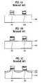
- FIGS. 1A to 1Iare cross-sectional diagrams showing a related art method of fabricating a transistor in a semiconductor device.
- an oxide layeris formed on a silicon substrate 100 , and a polysilicon layer is formed on the oxide layer. Photolithography is performed on the polysilicon layer and the oxide layer to form a gate oxide layer 101 and a gate 102 .
- an oxide layer 103is formed on the silicon substrate 100 including exposed surfaces of the gate oxide layer 101 and the gate 102 by oxidation to restore edges of the gate oxide layer 101 and to protect the silicon substrate 100 .
- FIG. 1CAs shown in FIG. 1C , light ion implantation is performed on the silicon substrate 100 to lightly doped regions 104 .
- An oxide layer 105 and a silicon nitride layer 106are stacked over the substrate 100 , as shown in FIG. 1D .
- the oxide layer 105 and the silicon nitride layer 106are etched back to remain on a sidewall of the gate 102 and the gate oxide layer 101 .
- a gate sidewall spacer 106 / 105is formed.
- a premetal dielectric (PMD) layer 109is formed on the silicon substrate 100 including the silicide layer 108 .
- FIG. 1Ishows an insulating interlayer 110 formed on the PMD layer 109 .
- a space between the gatesis narrowed due to the gate sidewall spacer 106 / 105 and the PMD layer 109 , a void V 1 is formed while depositing the insulating interlayer 110 .
- the void V 1can generate cracks or bridges in subsequent thermal and contact processes, thus lowering the yield and reliability of the semiconductor device.
- a gate oxide layer and a gateare formed on a semiconductor substrate.
- An oxide layer and a silicon nitride layerare stacked on the substrate.
- the stacked oxide and silicon nitride layersare etched back to expose a surface of the substrate.
- the silicon nitride layeris removed to form a gate sidewall spacer. Impurity ions are implanted into the substrate through the exposed surface of the substrate.
- FIGS. 1A to 1Iare cross-sectional diagrams showing a related art method of fabricating a transistor in a semiconductor device.
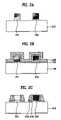
- FIGS. 2A to 2Hare cross-sectional diagrams showing a method of fabricating a transistor in a semiconductor device according to the present invention.
- FIGS. 2A to 2Hare cross-sectional diagrams showing a method of fabricating a transistor in a semiconductor device according to the present invention.
- an oxide layeris formed on a semiconductor substrate 200 , and a polysilicon layer is formed on the oxide layer. Photolithography is performed on the polysilicon layer and the oxide layer to form a gate oxide layer 201 and a gate 202 .
- the substrate 200is a silicon substrate.
- an oxide layer 205 and a silicon nitride layer 206are stacked on the substrate 200 .
- the oxide layer 205is formed for a gate sidewall spacer and the silicon nitride layer 206 is a sacrifice layer.
- a thickness of the oxide layer 205corresponds to an amount and depth profile of impurity ions subsequently provided by ion implantation
- a thickness of the silicon nitride layer 206corresponds to a size of the oxide layer 205 subsequently patterned.
- a predetermined size of the oxide layer 205will determine a range of an area of the substrate in which the impurity ions are subsequently implanted and prevent the impurity ions from diffusing into and/or beneath the gate oxide layer 201 to avoid parasitic capacitance.
- the nitride layer 206 and the oxide layer 205are etched back to remain on a sidewall of the gate 202 and the gate oxide layer 201 .
- a surface of the substrate 200acts as an etch-stop layer.
- a gate sidewall spacer, including layers 206 and 205is formed, and a portion of the substrate 200 between the gates 202 is exposed.
- the remaining silicon nitride layer 206 in FIG. 2Cis removed, preferably by a wet etch process. By this process, a sufficient space S can be provided between the gates 202 including the gate sidewall spacer 205 .
- ion implantationis performed on the substrate 200 using the gate sidewall spacer 205 as an ion implantation mask.
- ion-implanted source/drain regions 207 and 204are formed in the substrate 200 .
- additional oxidationcan be performed on the substrate 200 to adjust densities of the source/drain junctions 207 and 204 .
- silicidationis performed on the gate 202 and the source/drain regions 207 to form a silicide layer 208 .
- a premetal dielectric (PMD) layer 209is formed on the substrate 200 including the silicide layer 208 , as shown in FIG. 2G .
- an insulating interlayer 210is formed on the PMD layer 209 .
- the insulating layer 210is planarized and wiring is then performed to complete a logic process.
- a size of the source/drain region 204 for a LDDcan be adjusted by the thickness of the silicon nitride layer 206 , as shown in FIG. 2C .
- an overlap capacitance generated from the diffusing implanted ions under the gatecan be controlled by adjusting the thickness of the oxide layer 205 .
- the gate sidewall spacerdoes not sufficiently adjust densities between heavily and lightly doped regions, additional thermal oxidation can be selectively performed on the exposed surface of the silicon substrate to facilitate the barrier material adjustment in the ion implanted regions.
- the space S of sufficient sizecan be provided by removing the silicon nitride layer 206 in FIG. 2C prior to ion implantation, such that voids can be prevented from being formed while gap-filling using the insulating interlayer 210 .
- the present inventionprovides the following advantages or effects.
- the impurity ion profile and density in siliconcan be adjusted according to a kind, shape, and/or thickness of the material on the silicon, and the space between gates can be sufficiently secured to avoid the formation of voids, such that device reliability can be enhanced.
- the space of a sufficient sizecan be provided between the gate and a device isolation layer defining the active area of the substrate, such that a contact margin can be enhanced relative to a contact margin of the conventional device.
- the gate sidewall spacecan prevent the impurity ions from diffusing beneath the gate oxide layer, i.e., into the channel region, such that the impurity ions are not overlapping the gate.
- parasitic capacitanceis avoided, and device performance is enhanced.
Landscapes
- Engineering & Computer Science (AREA)
- Physics & Mathematics (AREA)
- Condensed Matter Physics & Semiconductors (AREA)
- General Physics & Mathematics (AREA)
- Manufacturing & Machinery (AREA)
- Computer Hardware Design (AREA)
- Microelectronics & Electronic Packaging (AREA)
- Power Engineering (AREA)
- Insulated Gate Type Field-Effect Transistor (AREA)
- Electrodes Of Semiconductors (AREA)
Abstract
Description
Claims (5)
Applications Claiming Priority (2)
| Application Number | Priority Date | Filing Date | Title |
|---|---|---|---|
| KR10-2003-0100513 | 2003-12-30 | ||
| KR1020030100513AKR100588656B1 (en) | 2003-12-30 | 2003-12-30 | Transistor Formation Method of Semiconductor Device |
Publications (2)
| Publication Number | Publication Date |
|---|---|
| US20050142777A1 US20050142777A1 (en) | 2005-06-30 |
| US7435669B2true US7435669B2 (en) | 2008-10-14 |
Family
ID=34698768
Family Applications (1)
| Application Number | Title | Priority Date | Filing Date |
|---|---|---|---|
| US11/024,678Expired - Fee RelatedUS7435669B2 (en) | 2003-12-30 | 2004-12-30 | Method of fabricating transistor in semiconductor device |
Country Status (2)
| Country | Link |
|---|---|
| US (1) | US7435669B2 (en) |
| KR (1) | KR100588656B1 (en) |
Cited By (1)
| Publication number | Priority date | Publication date | Assignee | Title |
|---|---|---|---|---|
| US20230377992A1 (en)* | 2018-10-22 | 2023-11-23 | Taiwan Semiconductor Manufacturing Company, Ltd. | Fusi gated device formation |
Families Citing this family (4)
| Publication number | Priority date | Publication date | Assignee | Title |
|---|---|---|---|---|
| KR100847834B1 (en)* | 2006-12-29 | 2008-07-23 | 동부일렉트로닉스 주식회사 | Semiconductor Device Having Gap Fill Insulator and Manufacturing Method Thereof |
| CN101872726B (en)* | 2010-05-28 | 2016-03-23 | 上海华虹宏力半导体制造有限公司 | The manufacture method of semiconductor device |
| CN104538455A (en)* | 2014-12-31 | 2015-04-22 | 上海天马有机发光显示技术有限公司 | Method for manufacturing lightly-doped drain region, thin film transistor and array substrate |
| CN111613628B (en)* | 2020-06-04 | 2022-12-09 | 武汉天马微电子有限公司 | An organic light emitting display panel and a display device |
Citations (5)
| Publication number | Priority date | Publication date | Assignee | Title |
|---|---|---|---|---|
| US4757026A (en)* | 1986-11-04 | 1988-07-12 | Intel Corporation | Source drain doping technique |
| US5334556A (en)* | 1993-03-23 | 1994-08-02 | Texas Instruments Incorporated | Method for improving gate oxide integrity using low temperature oxidation during source/drain anneal |
| US5770508A (en)* | 1997-03-17 | 1998-06-23 | United Microelectronics Corp. | Method of forming lightly doped drains in metalic oxide semiconductor components |
| US6235597B1 (en)* | 1999-08-06 | 2001-05-22 | International Business Machines Corporation | Semiconductor structure having reduced silicide resistance between closely spaced gates and method of fabrication |
| US6635966B2 (en)* | 2001-04-30 | 2003-10-21 | Hynix Semiconductor Inc. | Method for fabricating SRAM cell |
- 2003
- 2003-12-30KRKR1020030100513Apatent/KR100588656B1/ennot_activeExpired - Fee Related
- 2004
- 2004-12-30USUS11/024,678patent/US7435669B2/ennot_activeExpired - Fee Related
Patent Citations (5)
| Publication number | Priority date | Publication date | Assignee | Title |
|---|---|---|---|---|
| US4757026A (en)* | 1986-11-04 | 1988-07-12 | Intel Corporation | Source drain doping technique |
| US5334556A (en)* | 1993-03-23 | 1994-08-02 | Texas Instruments Incorporated | Method for improving gate oxide integrity using low temperature oxidation during source/drain anneal |
| US5770508A (en)* | 1997-03-17 | 1998-06-23 | United Microelectronics Corp. | Method of forming lightly doped drains in metalic oxide semiconductor components |
| US6235597B1 (en)* | 1999-08-06 | 2001-05-22 | International Business Machines Corporation | Semiconductor structure having reduced silicide resistance between closely spaced gates and method of fabrication |
| US6635966B2 (en)* | 2001-04-30 | 2003-10-21 | Hynix Semiconductor Inc. | Method for fabricating SRAM cell |
Cited By (2)
| Publication number | Priority date | Publication date | Assignee | Title |
|---|---|---|---|---|
| US20230377992A1 (en)* | 2018-10-22 | 2023-11-23 | Taiwan Semiconductor Manufacturing Company, Ltd. | Fusi gated device formation |
| US12439679B2 (en)* | 2018-10-22 | 2025-10-07 | Taiwan Semiconductor Manufacturing Company, Ltd. | FUSI gated device formation |
Also Published As
| Publication number | Publication date |
|---|---|
| US20050142777A1 (en) | 2005-06-30 |
| KR100588656B1 (en) | 2006-06-12 |
| KR20050070684A (en) | 2005-07-07 |
Similar Documents
| Publication | Publication Date | Title |
|---|---|---|
| US5959333A (en) | Reduction of dopant diffusion by the co-implantation of impurities into the transistor gate conductor | |
| JP4446949B2 (en) | Method for forming elevated salicide source / drain regions | |
| US6512299B1 (en) | Semiconductor device and a manufacturing process therefor | |
| US20020192868A1 (en) | Semiconductor device having LDD-type source/drain regions and fabrication method thereof | |
| US20080283879A1 (en) | Transistor having gate dielectric layer of partial thickness difference and method of fabricating the same | |
| JPH03248433A (en) | Manufacturing method of semiconductor device | |
| JPH1070191A (en) | Semiconductor device and manufacturing method thereof | |
| JP2655157B2 (en) | Manufacturing method of stacked MOS structure | |
| US7683406B2 (en) | Semiconductor device and method for forming the same | |
| US7915110B2 (en) | MOS transistor manufacturing | |
| JPH1174508A (en) | Semiconductor device and manufacturing method thereof | |
| US20070278589A1 (en) | Semiconductor device and fabrication method thereof | |
| JP2001127169A (en) | Semiconductor device and method of manufacturing the same | |
| US6300172B1 (en) | Method of field isolation in silicon-on-insulator technology | |
| KR100435261B1 (en) | Method of manufacturing in Split gate flash memory device | |
| US7435669B2 (en) | Method of fabricating transistor in semiconductor device | |
| JP2004273642A (en) | Semiconductor device and method of manufacturing the same | |
| US7521767B2 (en) | MOS transistor in a semiconductor device | |
| KR100695868B1 (en) | A device isolation film, a method of manufacturing the same, a semiconductor device having the same and a method of manufacturing the same | |
| US20020177284A1 (en) | Method of using sacrificial spacers to reduce short channel effect | |
| US6987038B2 (en) | Method for fabricating MOS field effect transistor | |
| US6765263B2 (en) | Semiconductor device and method for fabricating the same | |
| US20030119323A1 (en) | Method for fabricating transistor in semiconductor device | |
| JP3588566B2 (en) | Method for manufacturing semiconductor device | |
| KR100477535B1 (en) | Method of manufacturing semiconductor device |
Legal Events
| Date | Code | Title | Description |
|---|---|---|---|
| AS | Assignment | Owner name:DONGBUANAM SEMICONDUCTOR INC., KOREA, REPUBLIC OF Free format text:ASSIGNMENT OF ASSIGNORS INTEREST;ASSIGNOR:KIM, DAE KYEUN;REEL/FRAME:016139/0364 Effective date:20041221 | |
| AS | Assignment | Owner name:DONGBU ELECTRONICS CO., LTD.,KOREA, REPUBLIC OF Free format text:CHANGE OF NAME;ASSIGNOR:DONGBU-ANAM SEMICONDUCTOR, INC.;REEL/FRAME:017663/0468 Effective date:20060324 Owner name:DONGBU ELECTRONICS CO., LTD., KOREA, REPUBLIC OF Free format text:CHANGE OF NAME;ASSIGNOR:DONGBU-ANAM SEMICONDUCTOR, INC.;REEL/FRAME:017663/0468 Effective date:20060324 | |
| FEPP | Fee payment procedure | Free format text:PAYER NUMBER DE-ASSIGNED (ORIGINAL EVENT CODE: RMPN); ENTITY STATUS OF PATENT OWNER: LARGE ENTITY Free format text:PAYOR NUMBER ASSIGNED (ORIGINAL EVENT CODE: ASPN); ENTITY STATUS OF PATENT OWNER: LARGE ENTITY | |
| FPAY | Fee payment | Year of fee payment:4 | |
| REMI | Maintenance fee reminder mailed | ||
| LAPS | Lapse for failure to pay maintenance fees | ||
| STCH | Information on status: patent discontinuation | Free format text:PATENT EXPIRED DUE TO NONPAYMENT OF MAINTENANCE FEES UNDER 37 CFR 1.362 | |
| FP | Lapsed due to failure to pay maintenance fee | Effective date:20161014 |