US7435661B2 - Polish stop and sealing layer for manufacture of semiconductor devices with deep trench isolation - Google Patents
Polish stop and sealing layer for manufacture of semiconductor devices with deep trench isolationDownload PDFInfo
- Publication number
- US7435661B2 US7435661B2US11/341,010US34101006AUS7435661B2US 7435661 B2US7435661 B2US 7435661B2US 34101006 AUS34101006 AUS 34101006AUS 7435661 B2US7435661 B2US 7435661B2
- Authority
- US
- United States
- Prior art keywords
- layer
- dielectric layer
- substrate
- silicon dioxide
- deep trench
- Prior art date
- Legal status (The legal status is an assumption and is not a legal conclusion. Google has not performed a legal analysis and makes no representation as to the accuracy of the status listed.)
- Active, expires
Links
Images


Classifications
- H—ELECTRICITY
- H01—ELECTRIC ELEMENTS
- H01L—SEMICONDUCTOR DEVICES NOT COVERED BY CLASS H10
- H01L21/00—Processes or apparatus adapted for the manufacture or treatment of semiconductor or solid state devices or of parts thereof
- H01L21/70—Manufacture or treatment of devices consisting of a plurality of solid state components formed in or on a common substrate or of parts thereof; Manufacture of integrated circuit devices or of parts thereof
- H01L21/71—Manufacture of specific parts of devices defined in group H01L21/70
- H01L21/76—Making of isolation regions between components
- H01L21/763—Polycrystalline semiconductor regions
Definitions
- the present inventionrelates to semiconductor processing. More specifically, the invention is a fabrication method for deep trench isolation and a resulting integrated circuit structure.
- each element formed in a narrow region on the substrateis electrically isolated from adjacent elements such that the elements are not electrically influenced by each other.
- an isolation layer or isolation structureis commonly used.
- a fabrication techniqueuses an SOI substrate in which a buried oxide layer is formed below the device elements.
- a high performance semiconductor devicesuch as a central processing unit (CPU)
- the SOI type semiconductor devicein which an element region is completely isolated by an insulation layer is widely used. Deep trench isolation techniques are frequently employed to isolate device elements laterally.
- Formation of deep trench isolationcan be partially accomplished with low-cost dielectric films.
- Low-cost dielectric filmstypically have less desirable electrical characteristics (e.g., dielectric breakdown strength or higher shrinkage values) than a high-quality film.
- high-quality filmsare unsuitable for filling the deep trench.
- a high-quality dielectric filmis a better choice for filling shallow trench isolation (STI) regions and for producing cap layers over a deep trench fill layer.
- STIshallow trench isolation
- cap layersover a deep trench fill layer.
- both types of fillare present in a structure, only one film, preferably the high-quality film, should be exposed at the surface. If both film types are exposed, one of the two films will likely have a higher etch rate during subsequent cleaning and etching processes.
- polysilicon stringersare thin “strings” of polysilicon left along any steps or gaps on an uppermost surface topography of the substrate after etching operations. These stringers occur because the thickness of the polysilicon film is much thicker at a step or gap than in flat areas, by approximately the step height plus the polysilicon thickness. Overetching the polysilicon film to eliminate stringers is undesirable since (1) increased costs result from added or prolonged fabrication steps or operations; and (2) required conductive features may also be etched away.
- the polysilicon stringerscan result in electrical shorts between adjacent polysilicon conductors on a surface of the composite dielectric film. The electrical shorts can produce catastrophic failures in one or more active devices on an integrated circuit (IC) chip, consequently leading to low fabrication yield.
- ICintegrated circuit
- the present inventionis a method and resulting device that eliminates vertical steps or gaps in a deep trench isolation region and, thus, eliminates or drastically reduces a possibility of polysilicon stringers. Additionally, the invention allows an inexpensive dielectric material, for example a lower-quality silicon dioxide to be used to fill the deep trench and a higher quality oxide, in an electrically active region, to be used on an uppermost portion of the deep trench without either affecting device performance or increasing a possibility of forming polysilicon stringers.
- a dielectric materialfor example a lower-quality silicon dioxide to be used to fill the deep trench and a higher quality oxide, in an electrically active region
- an exemplary embodiment of the inventionis a method of fabricating an electrical isolation device and includes forming a first silicon dioxide layer on a first surface of a substrate, forming a first silicon nitride layer over the first silicon dioxide layer, and etching through a portion of the first silicon dioxide layer and the first silicon nitride layer, thereby exposing a portion of the first surface of the substrate.
- a shallow trenchis then etched into the substrate in a region substantially circumscribed by the exposed portion of the first surface of the substrate. Exposed sidewalls and a bottom region of the shallow trench are then oxidized, forming a liner oxide.
- a second silicon dioxide layeris conformally deposited, filling the shallow trench and covering at least a portion of the first silicon nitride layer.
- the second silicon dioxide layeris planarized (e.g., by chemical mechanical planarization (CMP)) to a level substantially coplanar with an uppermost surface of the first silicon nitride layer.
- CMPchemical mechanical planarization
- a second silicon nitride layeris then deposited over the planarized second silicon dioxide layer.
- the second silicon nitride layer and the second silicon dioxide layerare etched, exposing a region substantially circumscribed laterally by the shallow trench and a deep trench is etched in the exposed region.
- a third silicon dioxide layerfills the deep trench and covers at least a portion of the second silicon nitride layer.
- the third silicon dioxide layeris then planarized (e.g., by CMP) to a level substantially coplanar with an uppermost portion of the second silicon nitride layer.
- the third silicon dioxide layerin a region substantially circumscribed laterally by the deep trench, is partially etched into a concave region.
- the concave regionis filled with a fourth silicon dioxide layer.
- the fourth silicon dioxide layermay be comprised of a material having better electrical performance characteristics than material comprising the third silicon dioxide, or fill layer. Any remaining silicon nitride is then stripped.
- third and fourth silicon dioxide layersmay be different types of oxide with third oxide (i.e., the deep trench fill oxide) being of a lower quality than the fourth silicon dioxide layer (i.e., the layer in closest proximity to an active device region). Overall fabrication costs are thereby reduced without sacrificing the electrical performance of the active device.
- a region of the second silicon nitride layer overlaying the first silicon dioxide layer and the first silicon nitride layerprevents any gaps or vertical steps from forming.
- an uppermost portion of exposed planarized second oxide layer and the fourth oxide fill layerare continuous; there are no gaps between the two oxide regions.
- polysilicon deposition steps to form active devicese.g., MOSFETs
- underlying layershave no inaccessible vertical steps or gaps.
- FIGS. 1A-1Mshow various exemplary fabrication steps for producing a deep trench isolation structure of the present invention.
- FIGS. 2A-2Bshow various steps in fabricating a deep trench isolation structure of the prior art.
- the base substrate 101is a C-flat, silicon on insulator (SOI) over silicon substrate.
- the silicon cap layer 101 Ais approximately 2 ⁇ m (2000 nm) in thickness and is bonded to an SOI insulator layer 101 B.
- the base substrate 101may be a silicon wafer.
- another elemental group IV semiconductor or compound semiconductore.g., group III-V may be selected for the base substrate 101 .
- the base substrate 101is a semiconductor wafer
- the wafermay contain a buried oxide layer (not shown) placed below a polysilicon layer (not shown) to prevent transport of carriers through the underlying bulk semiconducting material.
- the polysiliconis then treated at an elevated temperature to reform crystalline (i.e., non-amorphous) silicon.
- the base substrate 101is formed from intrinsic silicon, thereby effectively limiting transport of carriers due to the high resistivity of intrinsic silicon.
- a first surface of the base substrate 101includes a pad oxide layer 103 , a first silicon nitride layer 105 A, and a first photoresist layer 107 .
- the first photoresist layer 107is patterned, baked, developed, and etched in accordance with techniques well known to a skilled artisan. Portions of the underlying pad oxide layer 103 and the first silicon nitride layer 105 A are then etched, exposing the first surface of the base substrate 101 . Etching may be accomplished through various wet etch (e.g., in hydrofluoric acid, such as contained in a standard buffered oxide etch (BOE), or orthophosphoric acid) or dry etch (e.g., reactive-ion etch (RIE)) techniques.
- hydrofluoric acidsuch as contained in a standard buffered oxide etch (BOE), or orthophosphoric acid
- RIEreactive-ion etch
- the shallow trenches 109are etched, in situ, as a follow-on dry etch step once the first silicon nitride layer 105 A and the pad oxide layer 103 have been opened. Any silicon-containing layers may be etched, for example, with potassium hydroxide (KOH) or tetra-methyl ammonium hydroxide (TMAH).
- KOHpotassium hydroxide
- TMAHtetra-methyl ammonium hydroxide
- An edge wall angle of the shallow trench 109 formed within the base substrate 101will depend on several factors such as a crystallographic orientation of the base substrate 101 and the type of etchant employed. The edge wall angle may be determined by the dry etch process chemistry and conditions used during the shallow trench etch step.
- the first photoresist layer 107is 8500 ⁇ (0.85 ⁇ m)
- the first silicon nitride layer 105 Ais 1000 ⁇ (0.1 ⁇ m)
- the pad oxideis a thermally grown silicon dioxide layer 180 ⁇ in thickness.
- the SOI silicon cap layer 101 Ais etched to a depth of 5000 ⁇ (0.5 ⁇ m).
- a first liner oxide 111is thermally grown on sidewalls of the shallow trench 109 .
- the first liner oxide 111could be deposited.
- a first oxide fill layer 113 Ais then conformally deposited.
- the first oxide fill layer 113 Amay be deposited by any of a variety of techniques such as chemical vapor deposition (CVD), low-pressure CVD (LPCVD), plasma-enhanced CVD (PECVD), or plasma-assisted CVD (PACVD).
- CVDchemical vapor deposition
- LPCVDlow-pressure CVD
- PECVDplasma-enhanced CVD
- PCVDplasma-assisted CVD
- the first liner oxide 111is 520 ⁇ thick and the first oxide fill layer 113 A is a high density plasma (HDP) deposition, 7000 ⁇ (0.7 ⁇ m) in thickness.
- HDPhigh density plasma
- a chemical-mechanical planarization (CMP) stepremoves a portion of the first oxide fill layer 113 A, producing a planarized first oxide layer 113 B, to a level essentially coplanar with a top portion of a planarized first nitride layer 105 B.
- CMPchemical-mechanical planarization
- a second silicon nitride layer 105 Cis then conformally deposited ( FIG. 1D ), followed by deposition of a second oxide layer 115 .
- the second silicon nitride layer 105 Cis about 500 ⁇ in thickness and the second oxide layer 115 is an HDP deposition, approximately 2000 ⁇ in thickness.
- a second photoresist layer 117is applied ( FIG. 1E ), patterned, developed, and etched. Portions of the underlying second oxide layer 115 , the second silicon nitride layer 105 C, the planarized first oxide layer 113 B, and the first liner oxide 111 are all etched, exposing a portion of the base substrate 101 and producing a dielectric trench etch window 119 .
- the second photoresist layer 117is then stripped ( FIG. 1F ) and the base substrate 101 is etched, producing a deep trench etch 121 . If the base substrate 101 is SOI over silicon, the silicon cap layer 101 A is etched through to the SOI insulator 101 B.
- the deep trench 121is etched to a depth of several micrometers. (The final device type being fabricated would be determinative of an exact depth required to provide effective electrical isolation.)
- the base substrate 101may be wet-etched or dry-etched to form the deep trench 121 .
- the deep trench etch 121is produced by RIE and is approximately 0.9 ⁇ m in width.
- the second oxide layer 115provides an etch stop protecting the second silicon nitride layer 105 C.
- the deep trench etch 121is oxidized, producing a second liner oxide 123 comprised of, for example, silicon dioxide assuming a silicon-containing base substrate 101 .
- the silicon nitride layers 105 B, 105 Cprovides an effective seal against diffusion of any oxidizing species (e.g., oxygen atoms (O) from steam (i.e., H 2 O) hydration or oxygen molecules (O 2 ) from dry-ox techniques) to portions of the base substrate which may, for example, serve as a channel region of a MOSFET device.
- An enlarged area “A” of FIG. 1Gindicates a sharp, non-oxidized corner region of an active channel.
- the second liner oxide 123provides a high quality oxide for enhanced device performance.
- the second liner oxide 123is thermally grown to approximately 520 ⁇ in thickness.
- a deep trench oxide fill layer 125provides a dielectric fill of the deep trench 121 .
- An LPTEOS (low pressure tetra-ethoxysilane) depositionprovides a deep fill that has good tensile performance and resists cracking; although a skilled artisan realizes that other low shrinkage dielectric fills and techniques could readily be used (e.g., PETEOS, ozone-TEOS, or an LPCVD oxide).
- Overfill from the deep trench 121 fill operationis at least partially removed in a densification process ( FIG. 1I ).
- a second CMP operationmay be employed.
- a portion of the densified deep trench oxide fill layer 125 and second oxide layer 115 overlying the second silicon nitride layer 105 Chas been stripped while concurrently fabricated, selectively-etched shallow trenches 127 have been formed.
- a high selectivity etchantis used to etch portions of the deep trench oxide fill layer 125 while etching little, if any, of the second silicon nitride layer 105 C.
- Such high-selectivity etchantsare well known in the semiconductor art.
- a high selectivity to either silicon or silicon dioxideis accomplished using CHF 3 /O 2 , CH 2 F 2 , or CH 3 F.
- Undercut on the planarized first oxide layer 113 Bis minimal. The minimal undercut is readily controlled by a combination of chemical, timing, and application choices which are known to a skilled artisan.
- An enlarged area “B” of FIG. 1Jshows a portion indicating controlled corner-oxidation is possible in a corner of the substrate 101 near the deep trench oxide fill layer 125 .
- a break, or rounding, of the cornerreduces a maximum electric field in this region during high voltage operations. Reducing the electric field strength raises a maximum voltage that can be applied without causing damage to surrounding dielectric materials or degrading dielectric material properties. Further, a large field in this area may lead to carrier trapping, resulting in potential channel inversion regions and potential device leakage. Thus, as design rules for high voltage devices are scaled downward, benefits of corner rounding are becoming increasingly significant.
- a height “H” of the shallow trench 127is approximately 0.2 ⁇ m-0.7 ⁇ m, although a skilled artisan will recognize the value of “H” will scale with changes in design rules. Additionally, controlling the depth of “H” allows a designer to control an amount of corner rounding required as a function of both design rule and applied maximum voltage.
- a fourth oxide fill layer 129is conformally deposited, followed by an additional CMP operation ( FIG. 1L ).
- the second silicon nitride layer 105 Cserves as a planarization stop point for the CMP operation.
- the silicon nitride layers 105 B, 105 Care selectively stripped ( FIG. 1M ) using, for example, hot phosphoric acid.
- Nitridemay also be anisotropically etched, for example, by RIE.
- polysilicon deposition steps to form active devicesis simplified if underlying layers have no inaccessible vertical steps or gaps.
- Vertical steps or gapscan lead to formation of polysilicon stringers.
- Polysilicon stringersare thin conductive “strings” of polysilicon left along any steps or gaps on an uppermost surface topography after etching operations. These stringers occur because the thickness of the polysilicon film is much thicker at a step or gap than in flat areas, by approximately the step height plus the polysilicon thickness. Overetching the polysilicon film to eliminate stringers is undesirable since required conductive features may also be etched away. Therefore, steps or gaps should be avoided.
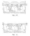
- FIG. 2Aillustrates how such steps or gaps are commonly formed in the prior art.
- FIG. 2Aincludes an HDP oxide cap layer 201 , a silicon nitride layer 203 , and a deep trench oxide fill layer 205 .
- Comparison of the prior art with the present inventiongraphically illustrates an advantageous feature of the second silicon nitride layer 105 C ( FIG. 1L ) of the present invention.
- CMPis attempted without the silicon nitride layer 105 C
- significant dishing of the dielectric layertakes place. Dishing is a feature common to CMP operations and occurs due to a difference in relative hardness levels of various planarized materials.
- Silicon nitrideis much harder (e.g., on a Mhos or Rockwell-C hardness scale) than silicon dioxide. Consequently, the oxide wears more quickly than the nitride and dishing results.
- the dishingcauses exposure of the junction between the dielectric layers and disparate physical characteristics and disparate etch rates during subsequent etch and clean operations
- deposition methodsmay produce a different effect in hardness and chemical characteristics of the same material. Therefore, an LPTEOS oxide will have a different etch rate from an HDP oxide. During subsequent processing, a junction of these differently deposited materials will form a vertical step which later causes a polysilicon stringer to form. Prior art processing of isolation regions of FIG. 2B illustrates this point.
- a vertical step 207e.g., hot phosphoric acid to remove nitride and BOE to remove oxide
- the etch rate of the LPTEOS oxidei.e., the deep trench oxide fill layer 205
- an etch rate of the capping dielectriccould be higher that that of the fill material for the deep trench.
- a vertical stepforms.
- the vertical step 207allows a subsequently deposited polysilicon layer (not shown) to be deposited more thickly in the vertical step 207 area, leaving a potential for polysilicon stringers.
- the polysilicon stringercauses shorts between parallel polysilicon conductors, thereby destroying the functionality of one or more IC components.
- the present inventioneliminates or minimizes the possibility of a vertical step being formed.
- TFHthin-film head
- AMLCDactive matrix liquid crystal display
- semiconductorshould be recognized as including at least the aforementioned as well as other related industries.
Landscapes
- Engineering & Computer Science (AREA)
- Chemical & Material Sciences (AREA)
- Crystallography & Structural Chemistry (AREA)
- Physics & Mathematics (AREA)
- Condensed Matter Physics & Semiconductors (AREA)
- General Physics & Mathematics (AREA)
- Manufacturing & Machinery (AREA)
- Computer Hardware Design (AREA)
- Microelectronics & Electronic Packaging (AREA)
- Power Engineering (AREA)
- Element Separation (AREA)
Abstract
Description
Claims (25)
Priority Applications (1)
| Application Number | Priority Date | Filing Date | Title |
|---|---|---|---|
| US11/341,010US7435661B2 (en) | 2006-01-27 | 2006-01-27 | Polish stop and sealing layer for manufacture of semiconductor devices with deep trench isolation |
Applications Claiming Priority (1)
| Application Number | Priority Date | Filing Date | Title |
|---|---|---|---|
| US11/341,010US7435661B2 (en) | 2006-01-27 | 2006-01-27 | Polish stop and sealing layer for manufacture of semiconductor devices with deep trench isolation |
Publications (2)
| Publication Number | Publication Date |
|---|---|
| US20070178660A1 US20070178660A1 (en) | 2007-08-02 |
| US7435661B2true US7435661B2 (en) | 2008-10-14 |
Family
ID=38322615
Family Applications (1)
| Application Number | Title | Priority Date | Filing Date |
|---|---|---|---|
| US11/341,010Active2026-05-26US7435661B2 (en) | 2006-01-27 | 2006-01-27 | Polish stop and sealing layer for manufacture of semiconductor devices with deep trench isolation |
Country Status (1)
| Country | Link |
|---|---|
| US (1) | US7435661B2 (en) |
Cited By (49)
| Publication number | Priority date | Publication date | Assignee | Title |
|---|---|---|---|---|
| US20080265363A1 (en)* | 2007-04-30 | 2008-10-30 | Jeffrey Peter Gambino | High power device isolation and integration |
| US7745352B2 (en) | 2007-08-27 | 2010-06-29 | Applied Materials, Inc. | Curing methods for silicon dioxide thin films deposited from alkoxysilane precursor with harp II process |
| US20100167496A1 (en)* | 2008-12-26 | 2010-07-01 | Jae-Hyoung Koo | Method for forming device isolation layer of semiconductor device and non-volatile memory device |
| US7790634B2 (en) | 2006-05-30 | 2010-09-07 | Applied Materials, Inc | Method for depositing and curing low-k films for gapfill and conformal film applications |
| US7803722B2 (en) | 2007-10-22 | 2010-09-28 | Applied Materials, Inc | Methods for forming a dielectric layer within trenches |
| US7825038B2 (en) | 2006-05-30 | 2010-11-02 | Applied Materials, Inc. | Chemical vapor deposition of high quality flow-like silicon dioxide using a silicon containing precursor and atomic oxygen |
| US7867923B2 (en) | 2007-10-22 | 2011-01-11 | Applied Materials, Inc. | High quality silicon oxide films by remote plasma CVD from disilane precursors |
| US7902080B2 (en) | 2006-05-30 | 2011-03-08 | Applied Materials, Inc. | Deposition-plasma cure cycle process to enhance film quality of silicon dioxide |
| US7935643B2 (en) | 2009-08-06 | 2011-05-03 | Applied Materials, Inc. | Stress management for tensile films |
| US7943531B2 (en) | 2007-10-22 | 2011-05-17 | Applied Materials, Inc. | Methods for forming a silicon oxide layer over a substrate |
| US7981763B1 (en)* | 2008-08-15 | 2011-07-19 | Novellus Systems, Inc. | Atomic layer removal for high aspect ratio gapfill |
| US7989365B2 (en) | 2009-08-18 | 2011-08-02 | Applied Materials, Inc. | Remote plasma source seasoning |
| US7994019B1 (en) | 2010-04-01 | 2011-08-09 | Applied Materials, Inc. | Silicon-ozone CVD with reduced pattern loading using incubation period deposition |
| US8043972B1 (en) | 2006-06-30 | 2011-10-25 | Novellus Systems, Inc. | Adsorption based material removal process |
| US8187486B1 (en) | 2007-12-13 | 2012-05-29 | Novellus Systems, Inc. | Modulating etch selectivity and etch rate of silicon nitride thin films |
| US8232176B2 (en)* | 2006-06-22 | 2012-07-31 | Applied Materials, Inc. | Dielectric deposition and etch back processes for bottom up gapfill |
| US8236708B2 (en) | 2010-03-09 | 2012-08-07 | Applied Materials, Inc. | Reduced pattern loading using bis(diethylamino)silane (C8H22N2Si) as silicon precursor |
| US8304351B2 (en) | 2010-01-07 | 2012-11-06 | Applied Materials, Inc. | In-situ ozone cure for radical-component CVD |
| US8318584B2 (en) | 2010-07-30 | 2012-11-27 | Applied Materials, Inc. | Oxide-rich liner layer for flowable CVD gapfill |
| US8329262B2 (en) | 2010-01-05 | 2012-12-11 | Applied Materials, Inc. | Dielectric film formation using inert gas excitation |
| US8357435B2 (en) | 2008-05-09 | 2013-01-22 | Applied Materials, Inc. | Flowable dielectric equipment and processes |
| US8445078B2 (en) | 2011-04-20 | 2013-05-21 | Applied Materials, Inc. | Low temperature silicon oxide conversion |
| US8449942B2 (en) | 2009-11-12 | 2013-05-28 | Applied Materials, Inc. | Methods of curing non-carbon flowable CVD films |
| US8450191B2 (en) | 2011-01-24 | 2013-05-28 | Applied Materials, Inc. | Polysilicon films by HDP-CVD |
| US8466073B2 (en) | 2011-06-03 | 2013-06-18 | Applied Materials, Inc. | Capping layer for reduced outgassing |
| US8476142B2 (en) | 2010-04-12 | 2013-07-02 | Applied Materials, Inc. | Preferential dielectric gapfill |
| US8524004B2 (en) | 2010-06-16 | 2013-09-03 | Applied Materials, Inc. | Loadlock batch ozone cure |
| US8551891B2 (en) | 2011-10-04 | 2013-10-08 | Applied Materials, Inc. | Remote plasma burn-in |
| US8563445B2 (en) | 2010-03-05 | 2013-10-22 | Applied Materials, Inc. | Conformal layers by radical-component CVD |
| US8617989B2 (en) | 2011-09-26 | 2013-12-31 | Applied Materials, Inc. | Liner property improvement |
| US8629067B2 (en) | 2009-12-30 | 2014-01-14 | Applied Materials, Inc. | Dielectric film growth with radicals produced using flexible nitrogen/hydrogen ratio |
| US8647992B2 (en) | 2010-01-06 | 2014-02-11 | Applied Materials, Inc. | Flowable dielectric using oxide liner |
| US8664127B2 (en) | 2010-10-15 | 2014-03-04 | Applied Materials, Inc. | Two silicon-containing precursors for gapfill enhancing dielectric liner |
| US8716154B2 (en) | 2011-03-04 | 2014-05-06 | Applied Materials, Inc. | Reduced pattern loading using silicon oxide multi-layers |
| US8741788B2 (en) | 2009-08-06 | 2014-06-03 | Applied Materials, Inc. | Formation of silicon oxide using non-carbon flowable CVD processes |
| US8889566B2 (en) | 2012-09-11 | 2014-11-18 | Applied Materials, Inc. | Low cost flowable dielectric films |
| US8980382B2 (en) | 2009-12-02 | 2015-03-17 | Applied Materials, Inc. | Oxygen-doping for non-carbon radical-component CVD films |
| US9018108B2 (en) | 2013-01-25 | 2015-04-28 | Applied Materials, Inc. | Low shrinkage dielectric films |
| US9285168B2 (en) | 2010-10-05 | 2016-03-15 | Applied Materials, Inc. | Module for ozone cure and post-cure moisture treatment |
| US9404178B2 (en) | 2011-07-15 | 2016-08-02 | Applied Materials, Inc. | Surface treatment and deposition for reduced outgassing |
| US9412581B2 (en) | 2014-07-16 | 2016-08-09 | Applied Materials, Inc. | Low-K dielectric gapfill by flowable deposition |
| US9425041B2 (en) | 2015-01-06 | 2016-08-23 | Lam Research Corporation | Isotropic atomic layer etch for silicon oxides using no activation |
| US9431268B2 (en) | 2015-01-05 | 2016-08-30 | Lam Research Corporation | Isotropic atomic layer etch for silicon and germanium oxides |
| US10283321B2 (en) | 2011-01-18 | 2019-05-07 | Applied Materials, Inc. | Semiconductor processing system and methods using capacitively coupled plasma |
| US11107674B2 (en) | 2019-01-24 | 2021-08-31 | Applied Materials, Inc. | Methods for depositing silicon nitride |
| US11380556B2 (en) | 2018-05-25 | 2022-07-05 | Lam Research Corporation | Thermal atomic layer etch with rapid temperature cycling |
| US11637022B2 (en) | 2018-07-09 | 2023-04-25 | Lam Research Corporation | Electron excitation atomic layer etch |
| US12009228B2 (en) | 2015-02-03 | 2024-06-11 | Applied Materials, Inc. | Low temperature chuck for plasma processing systems |
| US12280091B2 (en) | 2021-02-03 | 2025-04-22 | Lam Research Corporation | Etch selectivity control in atomic layer etching |
Families Citing this family (13)
| Publication number | Priority date | Publication date | Assignee | Title |
|---|---|---|---|---|
| US7767515B2 (en)* | 2006-02-27 | 2010-08-03 | Synopsys, Inc. | Managing integrated circuit stress using stress adjustment trenches |
| US7772083B2 (en)* | 2008-12-29 | 2010-08-10 | International Business Machines Corporation | Trench forming method and structure |
| US8796106B2 (en)* | 2010-03-30 | 2014-08-05 | Stmicroelectronics S.R.L. | Isolation trenches |
| US8546208B2 (en)* | 2011-08-19 | 2013-10-01 | International Business Machines Corporation | Isolation region fabrication for replacement gate processing |
| US9012300B2 (en)* | 2012-10-01 | 2015-04-21 | United Microelectronics Corp. | Manufacturing method for a shallow trench isolation |
| CN109216257B (en)* | 2017-07-03 | 2020-12-15 | 无锡华润上华科技有限公司 | Manufacturing method of isolation structure of LDMOS |
| DE102017218635B4 (en)* | 2017-10-18 | 2021-03-18 | Infineon Technologies Ag | Method for closing an access opening to a cavity and a MEMS component with a closing element |
| US10483153B2 (en)* | 2017-11-14 | 2019-11-19 | Taiwan Semiconductor Manufacturing Co., Ltd. | Deep trench isolation structure in semiconductor device |
| CN110911342A (en)* | 2018-09-14 | 2020-03-24 | 长鑫存储技术有限公司 | Shallow trench isolation structure and preparation method thereof |
| US11101168B2 (en)* | 2019-10-30 | 2021-08-24 | Taiwan Semiconductor Manufacturing Company, Ltd. | Profile of deep trench isolation structure for isolation of high-voltage devices |
| DE102020107390A1 (en) | 2019-10-30 | 2021-05-06 | Taiwan Semiconductor Manufacturing Co. Ltd. | PROFILE OF A DUCT INSULATION STRUCTURE FOR THE INSULATION OF HIGH VOLTAGE DEVICES |
| US12198926B2 (en)* | 2020-07-31 | 2025-01-14 | Psiquantum, Corp. | Silicon nitride films having reduced interfacial strain |
| CN114242650A (en)* | 2021-12-16 | 2022-03-25 | 上海华虹宏力半导体制造有限公司 | High-voltage LDMOS device and preparation method thereof |
Citations (11)
| Publication number | Priority date | Publication date | Assignee | Title |
|---|---|---|---|---|
| US5943578A (en)* | 1993-02-05 | 1999-08-24 | Kabushiki Kaisha Toshiba | Method of manufacturing a semiconductor device having an element isolating region |
| US6146970A (en) | 1998-05-26 | 2000-11-14 | Motorola Inc. | Capped shallow trench isolation and method of formation |
| US6403492B1 (en) | 2001-02-02 | 2002-06-11 | Advanced Micro Devices, Inc. | Method of manufacturing semiconductor devices with trench isolation |
| US6410403B1 (en)* | 2000-11-02 | 2002-06-25 | Promos Technologies, Inc. | Method for planarizing a shallow trench isolation |
| US6579801B1 (en) | 2001-11-30 | 2003-06-17 | Advanced Micro Devices, Inc. | Method for enhancing shallow trench top corner rounding using endpoint control of nitride layer etch process with appropriate etch front |
| US20050064678A1 (en)* | 2003-09-19 | 2005-03-24 | Atmel Germany Gmbh | Method of fabricating a semiconductor component with active regions separated by isolation trenches |
| US20050176214A1 (en)* | 2004-02-05 | 2005-08-11 | Kuan-Lun Chang | Method of forming a shallow trench-deep trench isolation region for a BiCMOS/CMOS technology |
| US6930027B2 (en)* | 2003-02-18 | 2005-08-16 | Freescale Semiconductor, Inc. | Method of manufacturing a semiconductor component |
| US20050287765A1 (en)* | 2004-06-29 | 2005-12-29 | Satoshi Onai | Method for manufacturing semiconductor device |
| US20060051932A1 (en)* | 2004-09-08 | 2006-03-09 | Haruki Yoneda | Semiconductor device and method for manufacturing semiconductor device |
| US7189628B1 (en)* | 2003-05-20 | 2007-03-13 | Lsi Logic Corporation | Fabrication of trenches with multiple depths on the same substrate |
- 2006
- 2006-01-27USUS11/341,010patent/US7435661B2/enactiveActive
Patent Citations (11)
| Publication number | Priority date | Publication date | Assignee | Title |
|---|---|---|---|---|
| US5943578A (en)* | 1993-02-05 | 1999-08-24 | Kabushiki Kaisha Toshiba | Method of manufacturing a semiconductor device having an element isolating region |
| US6146970A (en) | 1998-05-26 | 2000-11-14 | Motorola Inc. | Capped shallow trench isolation and method of formation |
| US6410403B1 (en)* | 2000-11-02 | 2002-06-25 | Promos Technologies, Inc. | Method for planarizing a shallow trench isolation |
| US6403492B1 (en) | 2001-02-02 | 2002-06-11 | Advanced Micro Devices, Inc. | Method of manufacturing semiconductor devices with trench isolation |
| US6579801B1 (en) | 2001-11-30 | 2003-06-17 | Advanced Micro Devices, Inc. | Method for enhancing shallow trench top corner rounding using endpoint control of nitride layer etch process with appropriate etch front |
| US6930027B2 (en)* | 2003-02-18 | 2005-08-16 | Freescale Semiconductor, Inc. | Method of manufacturing a semiconductor component |
| US7189628B1 (en)* | 2003-05-20 | 2007-03-13 | Lsi Logic Corporation | Fabrication of trenches with multiple depths on the same substrate |
| US20050064678A1 (en)* | 2003-09-19 | 2005-03-24 | Atmel Germany Gmbh | Method of fabricating a semiconductor component with active regions separated by isolation trenches |
| US20050176214A1 (en)* | 2004-02-05 | 2005-08-11 | Kuan-Lun Chang | Method of forming a shallow trench-deep trench isolation region for a BiCMOS/CMOS technology |
| US20050287765A1 (en)* | 2004-06-29 | 2005-12-29 | Satoshi Onai | Method for manufacturing semiconductor device |
| US20060051932A1 (en)* | 2004-09-08 | 2006-03-09 | Haruki Yoneda | Semiconductor device and method for manufacturing semiconductor device |
Non-Patent Citations (1)
| Title |
|---|
| Wolf and Tauber, Silicon Processing for the VLSI Era: vol. 1-Process Technology 2<SUP>nd </SUP>Edition, 2000, pp. 202-206.* |
Cited By (56)
| Publication number | Priority date | Publication date | Assignee | Title |
|---|---|---|---|---|
| US7790634B2 (en) | 2006-05-30 | 2010-09-07 | Applied Materials, Inc | Method for depositing and curing low-k films for gapfill and conformal film applications |
| US7902080B2 (en) | 2006-05-30 | 2011-03-08 | Applied Materials, Inc. | Deposition-plasma cure cycle process to enhance film quality of silicon dioxide |
| US7825038B2 (en) | 2006-05-30 | 2010-11-02 | Applied Materials, Inc. | Chemical vapor deposition of high quality flow-like silicon dioxide using a silicon containing precursor and atomic oxygen |
| US8232176B2 (en)* | 2006-06-22 | 2012-07-31 | Applied Materials, Inc. | Dielectric deposition and etch back processes for bottom up gapfill |
| US8043972B1 (en) | 2006-06-30 | 2011-10-25 | Novellus Systems, Inc. | Adsorption based material removal process |
| US20100207233A1 (en)* | 2007-04-30 | 2010-08-19 | International Business Machines Corporation | High power device isolation and integration |
| US20080265363A1 (en)* | 2007-04-30 | 2008-10-30 | Jeffrey Peter Gambino | High power device isolation and integration |
| US7781292B2 (en)* | 2007-04-30 | 2010-08-24 | International Business Machines Corporation | High power device isolation and integration |
| US8193563B2 (en) | 2007-04-30 | 2012-06-05 | International Business Machines Corporation | High power device isolation and integration |
| US7745352B2 (en) | 2007-08-27 | 2010-06-29 | Applied Materials, Inc. | Curing methods for silicon dioxide thin films deposited from alkoxysilane precursor with harp II process |
| US8242031B2 (en) | 2007-10-22 | 2012-08-14 | Applied Materials, Inc. | High quality silicon oxide films by remote plasma CVD from disilane precursors |
| US7943531B2 (en) | 2007-10-22 | 2011-05-17 | Applied Materials, Inc. | Methods for forming a silicon oxide layer over a substrate |
| US7803722B2 (en) | 2007-10-22 | 2010-09-28 | Applied Materials, Inc | Methods for forming a dielectric layer within trenches |
| US7867923B2 (en) | 2007-10-22 | 2011-01-11 | Applied Materials, Inc. | High quality silicon oxide films by remote plasma CVD from disilane precursors |
| US8617348B1 (en) | 2007-12-13 | 2013-12-31 | Novellus Systems, Inc. | Modulating etch selectivity and etch rate of silicon nitride thin films |
| US8187486B1 (en) | 2007-12-13 | 2012-05-29 | Novellus Systems, Inc. | Modulating etch selectivity and etch rate of silicon nitride thin films |
| US8357435B2 (en) | 2008-05-09 | 2013-01-22 | Applied Materials, Inc. | Flowable dielectric equipment and processes |
| US7981763B1 (en)* | 2008-08-15 | 2011-07-19 | Novellus Systems, Inc. | Atomic layer removal for high aspect ratio gapfill |
| US8278185B2 (en)* | 2008-12-26 | 2012-10-02 | Hynix Semiconductor Inc. | Method for forming device isolation layer of semiconductor device and non-volatile memory device |
| US20100167496A1 (en)* | 2008-12-26 | 2010-07-01 | Jae-Hyoung Koo | Method for forming device isolation layer of semiconductor device and non-volatile memory device |
| US8741788B2 (en) | 2009-08-06 | 2014-06-03 | Applied Materials, Inc. | Formation of silicon oxide using non-carbon flowable CVD processes |
| US7935643B2 (en) | 2009-08-06 | 2011-05-03 | Applied Materials, Inc. | Stress management for tensile films |
| US7989365B2 (en) | 2009-08-18 | 2011-08-02 | Applied Materials, Inc. | Remote plasma source seasoning |
| US8449942B2 (en) | 2009-11-12 | 2013-05-28 | Applied Materials, Inc. | Methods of curing non-carbon flowable CVD films |
| US8980382B2 (en) | 2009-12-02 | 2015-03-17 | Applied Materials, Inc. | Oxygen-doping for non-carbon radical-component CVD films |
| US8629067B2 (en) | 2009-12-30 | 2014-01-14 | Applied Materials, Inc. | Dielectric film growth with radicals produced using flexible nitrogen/hydrogen ratio |
| US8329262B2 (en) | 2010-01-05 | 2012-12-11 | Applied Materials, Inc. | Dielectric film formation using inert gas excitation |
| US8647992B2 (en) | 2010-01-06 | 2014-02-11 | Applied Materials, Inc. | Flowable dielectric using oxide liner |
| US8304351B2 (en) | 2010-01-07 | 2012-11-06 | Applied Materials, Inc. | In-situ ozone cure for radical-component CVD |
| US8563445B2 (en) | 2010-03-05 | 2013-10-22 | Applied Materials, Inc. | Conformal layers by radical-component CVD |
| US8236708B2 (en) | 2010-03-09 | 2012-08-07 | Applied Materials, Inc. | Reduced pattern loading using bis(diethylamino)silane (C8H22N2Si) as silicon precursor |
| US7994019B1 (en) | 2010-04-01 | 2011-08-09 | Applied Materials, Inc. | Silicon-ozone CVD with reduced pattern loading using incubation period deposition |
| US8476142B2 (en) | 2010-04-12 | 2013-07-02 | Applied Materials, Inc. | Preferential dielectric gapfill |
| US8524004B2 (en) | 2010-06-16 | 2013-09-03 | Applied Materials, Inc. | Loadlock batch ozone cure |
| US8318584B2 (en) | 2010-07-30 | 2012-11-27 | Applied Materials, Inc. | Oxide-rich liner layer for flowable CVD gapfill |
| US9285168B2 (en) | 2010-10-05 | 2016-03-15 | Applied Materials, Inc. | Module for ozone cure and post-cure moisture treatment |
| US8664127B2 (en) | 2010-10-15 | 2014-03-04 | Applied Materials, Inc. | Two silicon-containing precursors for gapfill enhancing dielectric liner |
| US10283321B2 (en) | 2011-01-18 | 2019-05-07 | Applied Materials, Inc. | Semiconductor processing system and methods using capacitively coupled plasma |
| US8450191B2 (en) | 2011-01-24 | 2013-05-28 | Applied Materials, Inc. | Polysilicon films by HDP-CVD |
| US8716154B2 (en) | 2011-03-04 | 2014-05-06 | Applied Materials, Inc. | Reduced pattern loading using silicon oxide multi-layers |
| US8445078B2 (en) | 2011-04-20 | 2013-05-21 | Applied Materials, Inc. | Low temperature silicon oxide conversion |
| US8466073B2 (en) | 2011-06-03 | 2013-06-18 | Applied Materials, Inc. | Capping layer for reduced outgassing |
| US9404178B2 (en) | 2011-07-15 | 2016-08-02 | Applied Materials, Inc. | Surface treatment and deposition for reduced outgassing |
| US8617989B2 (en) | 2011-09-26 | 2013-12-31 | Applied Materials, Inc. | Liner property improvement |
| US8551891B2 (en) | 2011-10-04 | 2013-10-08 | Applied Materials, Inc. | Remote plasma burn-in |
| US8889566B2 (en) | 2012-09-11 | 2014-11-18 | Applied Materials, Inc. | Low cost flowable dielectric films |
| US9018108B2 (en) | 2013-01-25 | 2015-04-28 | Applied Materials, Inc. | Low shrinkage dielectric films |
| US9412581B2 (en) | 2014-07-16 | 2016-08-09 | Applied Materials, Inc. | Low-K dielectric gapfill by flowable deposition |
| US9431268B2 (en) | 2015-01-05 | 2016-08-30 | Lam Research Corporation | Isotropic atomic layer etch for silicon and germanium oxides |
| US9425041B2 (en) | 2015-01-06 | 2016-08-23 | Lam Research Corporation | Isotropic atomic layer etch for silicon oxides using no activation |
| US10679868B2 (en) | 2015-01-06 | 2020-06-09 | Lam Research Corporation | Isotropic atomic layer etch for silicon oxides using no activation |
| US12009228B2 (en) | 2015-02-03 | 2024-06-11 | Applied Materials, Inc. | Low temperature chuck for plasma processing systems |
| US11380556B2 (en) | 2018-05-25 | 2022-07-05 | Lam Research Corporation | Thermal atomic layer etch with rapid temperature cycling |
| US11637022B2 (en) | 2018-07-09 | 2023-04-25 | Lam Research Corporation | Electron excitation atomic layer etch |
| US11107674B2 (en) | 2019-01-24 | 2021-08-31 | Applied Materials, Inc. | Methods for depositing silicon nitride |
| US12280091B2 (en) | 2021-02-03 | 2025-04-22 | Lam Research Corporation | Etch selectivity control in atomic layer etching |
Also Published As
| Publication number | Publication date |
|---|---|
| US20070178660A1 (en) | 2007-08-02 |
Similar Documents
| Publication | Publication Date | Title |
|---|---|---|
| US7435661B2 (en) | Polish stop and sealing layer for manufacture of semiconductor devices with deep trench isolation | |
| KR100338767B1 (en) | Trench Isolation structure and semiconductor device having the same, trench isolation method | |
| US5811315A (en) | Method of forming and planarizing deep isolation trenches in a silicon-on-insulator (SOI) structure | |
| US7049661B2 (en) | Semiconductor device having epitaxial layer | |
| US5930645A (en) | Shallow trench isolation formation with reduced polish stop thickness | |
| US6074927A (en) | Shallow trench isolation formation with trench wall spacer | |
| US6171962B1 (en) | Shallow trench isolation formation without planarization mask | |
| US6306723B1 (en) | Method to form shallow trench isolations without a chemical mechanical polish | |
| US7705417B2 (en) | Semiconductor device and method of fabricating isolation region | |
| JP2008533705A (en) | Fabrication of carrier substrate contacts to trench-isolated SOI integrated circuits with high voltage components | |
| US20080206955A1 (en) | Method of Forming an Isolation Film in a Semiconductor Device | |
| US6130467A (en) | Shallow trench isolation with spacers for improved gate oxide quality | |
| US5882981A (en) | Mesa isolation Refill Process for Silicon on Insulator Technology Using Flowage Oxides as the Refill Material | |
| US6521510B1 (en) | Method for shallow trench isolation with removal of strained island edges | |
| US20110281416A1 (en) | Manufacturing method of semiconductor device | |
| US5970363A (en) | Shallow trench isolation formation with improved trench edge oxide | |
| US6358785B1 (en) | Method for forming shallow trench isolation structures | |
| US5970362A (en) | Simplified shallow trench isolation formation with no polish stop | |
| US6124183A (en) | Shallow trench isolation formation with simplified reverse planarization mask | |
| US11798836B2 (en) | Semiconductor isolation structure and method of making the same | |
| KR100515181B1 (en) | Method for producing semiconductor device | |
| US6342432B1 (en) | Shallow trench isolation formation without planarization mask | |
| US6893940B2 (en) | Method of manufacturing semiconductor device | |
| US9437674B2 (en) | Insulating trench forming method | |
| US6380047B1 (en) | Shallow trench isolation formation with two source/drain masks and simplified planarization mask |
Legal Events
| Date | Code | Title | Description |
|---|---|---|---|
| AS | Assignment | Owner name:ATMEL CORPORATION, CALIFORNIA Free format text:ASSIGNMENT OF ASSIGNORS INTEREST;ASSIGNORS:MILLER, GAYLE;BROWN, ERIC;REEL/FRAME:017737/0096 Effective date:20060123 | |
| FEPP | Fee payment procedure | Free format text:PAYOR NUMBER ASSIGNED (ORIGINAL EVENT CODE: ASPN); ENTITY STATUS OF PATENT OWNER: LARGE ENTITY | |
| STCF | Information on status: patent grant | Free format text:PATENTED CASE | |
| CC | Certificate of correction | ||
| FPAY | Fee payment | Year of fee payment:4 | |
| AS | Assignment | Owner name:MORGAN STANLEY SENIOR FUNDING, INC. AS ADMINISTRATIVE AGENT, NEW YORK Free format text:PATENT SECURITY AGREEMENT;ASSIGNOR:ATMEL CORPORATION;REEL/FRAME:031912/0173 Effective date:20131206 Owner name:MORGAN STANLEY SENIOR FUNDING, INC. AS ADMINISTRAT Free format text:PATENT SECURITY AGREEMENT;ASSIGNOR:ATMEL CORPORATION;REEL/FRAME:031912/0173 Effective date:20131206 | |
| FPAY | Fee payment | Year of fee payment:8 | |
| AS | Assignment | Owner name:ATMEL CORPORATION, CALIFORNIA Free format text:TERMINATION AND RELEASE OF SECURITY INTEREST IN PATENT COLLATERAL;ASSIGNOR:MORGAN STANLEY SENIOR FUNDING, INC.;REEL/FRAME:038376/0001 Effective date:20160404 | |
| AS | Assignment | Owner name:JPMORGAN CHASE BANK, N.A., AS ADMINISTRATIVE AGENT, ILLINOIS Free format text:SECURITY INTEREST;ASSIGNOR:ATMEL CORPORATION;REEL/FRAME:041715/0747 Effective date:20170208 Owner name:JPMORGAN CHASE BANK, N.A., AS ADMINISTRATIVE AGENT Free format text:SECURITY INTEREST;ASSIGNOR:ATMEL CORPORATION;REEL/FRAME:041715/0747 Effective date:20170208 | |
| AS | Assignment | Owner name:JPMORGAN CHASE BANK, N.A., AS ADMINISTRATIVE AGENT, ILLINOIS Free format text:SECURITY INTEREST;ASSIGNORS:MICROCHIP TECHNOLOGY INCORPORATED;SILICON STORAGE TECHNOLOGY, INC.;ATMEL CORPORATION;AND OTHERS;REEL/FRAME:046426/0001 Effective date:20180529 Owner name:JPMORGAN CHASE BANK, N.A., AS ADMINISTRATIVE AGENT Free format text:SECURITY INTEREST;ASSIGNORS:MICROCHIP TECHNOLOGY INCORPORATED;SILICON STORAGE TECHNOLOGY, INC.;ATMEL CORPORATION;AND OTHERS;REEL/FRAME:046426/0001 Effective date:20180529 | |
| AS | Assignment | Owner name:WELLS FARGO BANK, NATIONAL ASSOCIATION, AS NOTES COLLATERAL AGENT, CALIFORNIA Free format text:SECURITY INTEREST;ASSIGNORS:MICROCHIP TECHNOLOGY INCORPORATED;SILICON STORAGE TECHNOLOGY, INC.;ATMEL CORPORATION;AND OTHERS;REEL/FRAME:047103/0206 Effective date:20180914 Owner name:WELLS FARGO BANK, NATIONAL ASSOCIATION, AS NOTES C Free format text:SECURITY INTEREST;ASSIGNORS:MICROCHIP TECHNOLOGY INCORPORATED;SILICON STORAGE TECHNOLOGY, INC.;ATMEL CORPORATION;AND OTHERS;REEL/FRAME:047103/0206 Effective date:20180914 | |
| MAFP | Maintenance fee payment | Free format text:PAYMENT OF MAINTENANCE FEE, 12TH YEAR, LARGE ENTITY (ORIGINAL EVENT CODE: M1553); ENTITY STATUS OF PATENT OWNER: LARGE ENTITY Year of fee payment:12 | |
| AS | Assignment | Owner name:JPMORGAN CHASE BANK, N.A., AS ADMINISTRATIVE AGENT, DELAWARE Free format text:SECURITY INTEREST;ASSIGNORS:MICROCHIP TECHNOLOGY INC.;SILICON STORAGE TECHNOLOGY, INC.;ATMEL CORPORATION;AND OTHERS;REEL/FRAME:053311/0305 Effective date:20200327 | |
| AS | Assignment | Owner name:MICROCHIP TECHNOLOGY INC., ARIZONA Free format text:RELEASE BY SECURED PARTY;ASSIGNOR:JPMORGAN CHASE BANK, N.A, AS ADMINISTRATIVE AGENT;REEL/FRAME:053466/0011 Effective date:20200529 Owner name:MICROSEMI STORAGE SOLUTIONS, INC., ARIZONA Free format text:RELEASE BY SECURED PARTY;ASSIGNOR:JPMORGAN CHASE BANK, N.A, AS ADMINISTRATIVE AGENT;REEL/FRAME:053466/0011 Effective date:20200529 Owner name:MICROSEMI CORPORATION, CALIFORNIA Free format text:RELEASE BY SECURED PARTY;ASSIGNOR:JPMORGAN CHASE BANK, N.A, AS ADMINISTRATIVE AGENT;REEL/FRAME:053466/0011 Effective date:20200529 Owner name:SILICON STORAGE TECHNOLOGY, INC., ARIZONA Free format text:RELEASE BY SECURED PARTY;ASSIGNOR:JPMORGAN CHASE BANK, N.A, AS ADMINISTRATIVE AGENT;REEL/FRAME:053466/0011 Effective date:20200529 Owner name:ATMEL CORPORATION, ARIZONA Free format text:RELEASE BY SECURED PARTY;ASSIGNOR:JPMORGAN CHASE BANK, N.A, AS ADMINISTRATIVE AGENT;REEL/FRAME:053466/0011 Effective date:20200529 | |
| AS | Assignment | Owner name:WELLS FARGO BANK, NATIONAL ASSOCIATION, MINNESOTA Free format text:SECURITY INTEREST;ASSIGNORS:MICROCHIP TECHNOLOGY INC.;SILICON STORAGE TECHNOLOGY, INC.;ATMEL CORPORATION;AND OTHERS;REEL/FRAME:053468/0705 Effective date:20200529 | |
| AS | Assignment | Owner name:WELLS FARGO BANK, NATIONAL ASSOCIATION, AS COLLATERAL AGENT, MINNESOTA Free format text:SECURITY INTEREST;ASSIGNORS:MICROCHIP TECHNOLOGY INCORPORATED;SILICON STORAGE TECHNOLOGY, INC.;ATMEL CORPORATION;AND OTHERS;REEL/FRAME:055671/0612 Effective date:20201217 | |
| AS | Assignment | Owner name:WELLS FARGO BANK, NATIONAL ASSOCIATION, AS NOTES COLLATERAL AGENT, MINNESOTA Free format text:SECURITY INTEREST;ASSIGNORS:MICROCHIP TECHNOLOGY INCORPORATED;SILICON STORAGE TECHNOLOGY, INC.;ATMEL CORPORATION;AND OTHERS;REEL/FRAME:057935/0474 Effective date:20210528 | |
| AS | Assignment | Owner name:MICROSEMI STORAGE SOLUTIONS, INC., ARIZONA Free format text:RELEASE BY SECURED PARTY;ASSIGNOR:JPMORGAN CHASE BANK, N.A., AS ADMINISTRATIVE AGENT;REEL/FRAME:059333/0222 Effective date:20220218 Owner name:MICROSEMI CORPORATION, ARIZONA Free format text:RELEASE BY SECURED PARTY;ASSIGNOR:JPMORGAN CHASE BANK, N.A., AS ADMINISTRATIVE AGENT;REEL/FRAME:059333/0222 Effective date:20220218 Owner name:ATMEL CORPORATION, ARIZONA Free format text:RELEASE BY SECURED PARTY;ASSIGNOR:JPMORGAN CHASE BANK, N.A., AS ADMINISTRATIVE AGENT;REEL/FRAME:059333/0222 Effective date:20220218 Owner name:SILICON STORAGE TECHNOLOGY, INC., ARIZONA Free format text:RELEASE BY SECURED PARTY;ASSIGNOR:JPMORGAN CHASE BANK, N.A., AS ADMINISTRATIVE AGENT;REEL/FRAME:059333/0222 Effective date:20220218 Owner name:MICROCHIP TECHNOLOGY INCORPORATED, ARIZONA Free format text:RELEASE BY SECURED PARTY;ASSIGNOR:JPMORGAN CHASE BANK, N.A., AS ADMINISTRATIVE AGENT;REEL/FRAME:059333/0222 Effective date:20220218 | |
| AS | Assignment | Owner name:ATMEL CORPORATION, ARIZONA Free format text:RELEASE BY SECURED PARTY;ASSIGNOR:JPMORGAN CHASE BANK, N.A., AS ADMINISTRATIVE AGENT;REEL/FRAME:059262/0105 Effective date:20220218 | |
| AS | Assignment | Owner name:MICROSEMI STORAGE SOLUTIONS, INC., ARIZONA Free format text:RELEASE BY SECURED PARTY;ASSIGNOR:WELLS FARGO BANK, NATIONAL ASSOCIATION, AS NOTES COLLATERAL AGENT;REEL/FRAME:059358/0001 Effective date:20220228 Owner name:MICROSEMI CORPORATION, ARIZONA Free format text:RELEASE BY SECURED PARTY;ASSIGNOR:WELLS FARGO BANK, NATIONAL ASSOCIATION, AS NOTES COLLATERAL AGENT;REEL/FRAME:059358/0001 Effective date:20220228 Owner name:ATMEL CORPORATION, ARIZONA Free format text:RELEASE BY SECURED PARTY;ASSIGNOR:WELLS FARGO BANK, NATIONAL ASSOCIATION, AS NOTES COLLATERAL AGENT;REEL/FRAME:059358/0001 Effective date:20220228 Owner name:SILICON STORAGE TECHNOLOGY, INC., ARIZONA Free format text:RELEASE BY SECURED PARTY;ASSIGNOR:WELLS FARGO BANK, NATIONAL ASSOCIATION, AS NOTES COLLATERAL AGENT;REEL/FRAME:059358/0001 Effective date:20220228 Owner name:MICROCHIP TECHNOLOGY INCORPORATED, ARIZONA Free format text:RELEASE BY SECURED PARTY;ASSIGNOR:WELLS FARGO BANK, NATIONAL ASSOCIATION, AS NOTES COLLATERAL AGENT;REEL/FRAME:059358/0001 Effective date:20220228 | |
| AS | Assignment | Owner name:MICROSEMI STORAGE SOLUTIONS, INC., ARIZONA Free format text:RELEASE BY SECURED PARTY;ASSIGNOR:WELLS FARGO BANK, NATIONAL ASSOCIATION, AS NOTES COLLATERAL AGENT;REEL/FRAME:059863/0400 Effective date:20220228 Owner name:MICROSEMI CORPORATION, ARIZONA Free format text:RELEASE BY SECURED PARTY;ASSIGNOR:WELLS FARGO BANK, NATIONAL ASSOCIATION, AS NOTES COLLATERAL AGENT;REEL/FRAME:059863/0400 Effective date:20220228 Owner name:ATMEL CORPORATION, ARIZONA Free format text:RELEASE BY SECURED PARTY;ASSIGNOR:WELLS FARGO BANK, NATIONAL ASSOCIATION, AS NOTES COLLATERAL AGENT;REEL/FRAME:059863/0400 Effective date:20220228 Owner name:SILICON STORAGE TECHNOLOGY, INC., ARIZONA Free format text:RELEASE BY SECURED PARTY;ASSIGNOR:WELLS FARGO BANK, NATIONAL ASSOCIATION, AS NOTES COLLATERAL AGENT;REEL/FRAME:059863/0400 Effective date:20220228 Owner name:MICROCHIP TECHNOLOGY INCORPORATED, ARIZONA Free format text:RELEASE BY SECURED PARTY;ASSIGNOR:WELLS FARGO BANK, NATIONAL ASSOCIATION, AS NOTES COLLATERAL AGENT;REEL/FRAME:059863/0400 Effective date:20220228 | |
| AS | Assignment | Owner name:MICROSEMI STORAGE SOLUTIONS, INC., ARIZONA Free format text:RELEASE BY SECURED PARTY;ASSIGNOR:WELLS FARGO BANK, NATIONAL ASSOCIATION, AS NOTES COLLATERAL AGENT;REEL/FRAME:059363/0001 Effective date:20220228 Owner name:MICROSEMI CORPORATION, ARIZONA Free format text:RELEASE BY SECURED PARTY;ASSIGNOR:WELLS FARGO BANK, NATIONAL ASSOCIATION, AS NOTES COLLATERAL AGENT;REEL/FRAME:059363/0001 Effective date:20220228 Owner name:ATMEL CORPORATION, ARIZONA Free format text:RELEASE BY SECURED PARTY;ASSIGNOR:WELLS FARGO BANK, NATIONAL ASSOCIATION, AS NOTES COLLATERAL AGENT;REEL/FRAME:059363/0001 Effective date:20220228 Owner name:SILICON STORAGE TECHNOLOGY, INC., ARIZONA Free format text:RELEASE BY SECURED PARTY;ASSIGNOR:WELLS FARGO BANK, NATIONAL ASSOCIATION, AS NOTES COLLATERAL AGENT;REEL/FRAME:059363/0001 Effective date:20220228 Owner name:MICROCHIP TECHNOLOGY INCORPORATED, ARIZONA Free format text:RELEASE BY SECURED PARTY;ASSIGNOR:WELLS FARGO BANK, NATIONAL ASSOCIATION, AS NOTES COLLATERAL AGENT;REEL/FRAME:059363/0001 Effective date:20220228 | |
| AS | Assignment | Owner name:MICROSEMI STORAGE SOLUTIONS, INC., ARIZONA Free format text:RELEASE BY SECURED PARTY;ASSIGNOR:WELLS FARGO BANK, NATIONAL ASSOCIATION, AS NOTES COLLATERAL AGENT;REEL/FRAME:060894/0437 Effective date:20220228 Owner name:MICROSEMI CORPORATION, ARIZONA Free format text:RELEASE BY SECURED PARTY;ASSIGNOR:WELLS FARGO BANK, NATIONAL ASSOCIATION, AS NOTES COLLATERAL AGENT;REEL/FRAME:060894/0437 Effective date:20220228 Owner name:ATMEL CORPORATION, ARIZONA Free format text:RELEASE BY SECURED PARTY;ASSIGNOR:WELLS FARGO BANK, NATIONAL ASSOCIATION, AS NOTES COLLATERAL AGENT;REEL/FRAME:060894/0437 Effective date:20220228 Owner name:SILICON STORAGE TECHNOLOGY, INC., ARIZONA Free format text:RELEASE BY SECURED PARTY;ASSIGNOR:WELLS FARGO BANK, NATIONAL ASSOCIATION, AS NOTES COLLATERAL AGENT;REEL/FRAME:060894/0437 Effective date:20220228 Owner name:MICROCHIP TECHNOLOGY INCORPORATED, ARIZONA Free format text:RELEASE BY SECURED PARTY;ASSIGNOR:WELLS FARGO BANK, NATIONAL ASSOCIATION, AS NOTES COLLATERAL AGENT;REEL/FRAME:060894/0437 Effective date:20220228 |