US7435625B2 - Semiconductor device with reduced package cross-talk and loss - Google Patents
Semiconductor device with reduced package cross-talk and lossDownload PDFInfo
- Publication number
- US7435625B2 US7435625B2US11/257,802US25780205AUS7435625B2US 7435625 B2US7435625 B2US 7435625B2US 25780205 AUS25780205 AUS 25780205AUS 7435625 B2US7435625 B2US 7435625B2
- Authority
- US
- United States
- Prior art keywords
- die
- buffer region
- covering
- filler
- dielectric constant
- Prior art date
- Legal status (The legal status is an assumption and is not a legal conclusion. Google has not performed a legal analysis and makes no representation as to the accuracy of the status listed.)
- Active, expires
Links
Images


Classifications
- H—ELECTRICITY
- H01—ELECTRIC ELEMENTS
- H01L—SEMICONDUCTOR DEVICES NOT COVERED BY CLASS H10
- H01L23/00—Details of semiconductor or other solid state devices
- H01L23/28—Encapsulations, e.g. encapsulating layers, coatings, e.g. for protection
- H01L23/31—Encapsulations, e.g. encapsulating layers, coatings, e.g. for protection characterised by the arrangement or shape
- H01L23/3107—Encapsulations, e.g. encapsulating layers, coatings, e.g. for protection characterised by the arrangement or shape the device being completely enclosed
- H01L23/3135—Double encapsulation or coating and encapsulation
- H—ELECTRICITY
- H01—ELECTRIC ELEMENTS
- H01L—SEMICONDUCTOR DEVICES NOT COVERED BY CLASS H10
- H01L23/00—Details of semiconductor or other solid state devices
- H01L23/28—Encapsulations, e.g. encapsulating layers, coatings, e.g. for protection
- H—ELECTRICITY
- H01—ELECTRIC ELEMENTS
- H01L—SEMICONDUCTOR DEVICES NOT COVERED BY CLASS H10
- H01L23/00—Details of semiconductor or other solid state devices
- H01L23/02—Containers; Seals
- H—ELECTRICITY
- H01—ELECTRIC ELEMENTS
- H01L—SEMICONDUCTOR DEVICES NOT COVERED BY CLASS H10
- H01L23/00—Details of semiconductor or other solid state devices
- H01L23/28—Encapsulations, e.g. encapsulating layers, coatings, e.g. for protection
- H01L23/29—Encapsulations, e.g. encapsulating layers, coatings, e.g. for protection characterised by the material, e.g. carbon
- H01L23/293—Organic, e.g. plastic
- H01L23/295—Organic, e.g. plastic containing a filler
- H—ELECTRICITY
- H01—ELECTRIC ELEMENTS
- H01L—SEMICONDUCTOR DEVICES NOT COVERED BY CLASS H10
- H01L23/00—Details of semiconductor or other solid state devices
- H01L23/34—Arrangements for cooling, heating, ventilating or temperature compensation ; Temperature sensing arrangements
- H01L23/42—Fillings or auxiliary members in containers or encapsulations selected or arranged to facilitate heating or cooling
- H01L23/433—Auxiliary members in containers characterised by their shape, e.g. pistons
- H01L23/4334—Auxiliary members in encapsulations
- H—ELECTRICITY
- H01—ELECTRIC ELEMENTS
- H01L—SEMICONDUCTOR DEVICES NOT COVERED BY CLASS H10
- H01L2224/00—Indexing scheme for arrangements for connecting or disconnecting semiconductor or solid-state bodies and methods related thereto as covered by H01L24/00
- H01L2224/01—Means for bonding being attached to, or being formed on, the surface to be connected, e.g. chip-to-package, die-attach, "first-level" interconnects; Manufacturing methods related thereto
- H01L2224/02—Bonding areas; Manufacturing methods related thereto
- H01L2224/04—Structure, shape, material or disposition of the bonding areas prior to the connecting process
- H01L2224/05—Structure, shape, material or disposition of the bonding areas prior to the connecting process of an individual bonding area
- H01L2224/0554—External layer
- H01L2224/0555—Shape
- H01L2224/05552—Shape in top view
- H01L2224/05553—Shape in top view being rectangular
- H—ELECTRICITY
- H01—ELECTRIC ELEMENTS
- H01L—SEMICONDUCTOR DEVICES NOT COVERED BY CLASS H10
- H01L2224/00—Indexing scheme for arrangements for connecting or disconnecting semiconductor or solid-state bodies and methods related thereto as covered by H01L24/00
- H01L2224/01—Means for bonding being attached to, or being formed on, the surface to be connected, e.g. chip-to-package, die-attach, "first-level" interconnects; Manufacturing methods related thereto
- H01L2224/42—Wire connectors; Manufacturing methods related thereto
- H01L2224/47—Structure, shape, material or disposition of the wire connectors after the connecting process
- H01L2224/48—Structure, shape, material or disposition of the wire connectors after the connecting process of an individual wire connector
- H01L2224/481—Disposition
- H01L2224/48151—Connecting between a semiconductor or solid-state body and an item not being a semiconductor or solid-state body, e.g. chip-to-substrate, chip-to-passive
- H01L2224/48221—Connecting between a semiconductor or solid-state body and an item not being a semiconductor or solid-state body, e.g. chip-to-substrate, chip-to-passive the body and the item being stacked
- H01L2224/48245—Connecting between a semiconductor or solid-state body and an item not being a semiconductor or solid-state body, e.g. chip-to-substrate, chip-to-passive the body and the item being stacked the item being metallic
- H01L2224/48247—Connecting between a semiconductor or solid-state body and an item not being a semiconductor or solid-state body, e.g. chip-to-substrate, chip-to-passive the body and the item being stacked the item being metallic connecting the wire to a bond pad of the item
- H—ELECTRICITY
- H01—ELECTRIC ELEMENTS
- H01L—SEMICONDUCTOR DEVICES NOT COVERED BY CLASS H10
- H01L2224/00—Indexing scheme for arrangements for connecting or disconnecting semiconductor or solid-state bodies and methods related thereto as covered by H01L24/00
- H01L2224/93—Batch processes
- H01L2224/95—Batch processes at chip-level, i.e. with connecting carried out on a plurality of singulated devices, i.e. on diced chips
- H01L2224/97—Batch processes at chip-level, i.e. with connecting carried out on a plurality of singulated devices, i.e. on diced chips the devices being connected to a common substrate, e.g. interposer, said common substrate being separable into individual assemblies after connecting
- H—ELECTRICITY
- H01—ELECTRIC ELEMENTS
- H01L—SEMICONDUCTOR DEVICES NOT COVERED BY CLASS H10
- H01L24/00—Arrangements for connecting or disconnecting semiconductor or solid-state bodies; Methods or apparatus related thereto
- H01L24/01—Means for bonding being attached to, or being formed on, the surface to be connected, e.g. chip-to-package, die-attach, "first-level" interconnects; Manufacturing methods related thereto
- H01L24/42—Wire connectors; Manufacturing methods related thereto
- H01L24/47—Structure, shape, material or disposition of the wire connectors after the connecting process
- H01L24/48—Structure, shape, material or disposition of the wire connectors after the connecting process of an individual wire connector
- H—ELECTRICITY
- H01—ELECTRIC ELEMENTS
- H01L—SEMICONDUCTOR DEVICES NOT COVERED BY CLASS H10
- H01L2924/00—Indexing scheme for arrangements or methods for connecting or disconnecting semiconductor or solid-state bodies as covered by H01L24/00
- H01L2924/0001—Technical content checked by a classifier
- H01L2924/00014—Technical content checked by a classifier the subject-matter covered by the group, the symbol of which is combined with the symbol of this group, being disclosed without further technical details
- H—ELECTRICITY
- H01—ELECTRIC ELEMENTS
- H01L—SEMICONDUCTOR DEVICES NOT COVERED BY CLASS H10
- H01L2924/00—Indexing scheme for arrangements or methods for connecting or disconnecting semiconductor or solid-state bodies as covered by H01L24/00
- H01L2924/01—Chemical elements
- H01L2924/01021—Scandium [Sc]
- H—ELECTRICITY
- H01—ELECTRIC ELEMENTS
- H01L—SEMICONDUCTOR DEVICES NOT COVERED BY CLASS H10
- H01L2924/00—Indexing scheme for arrangements or methods for connecting or disconnecting semiconductor or solid-state bodies as covered by H01L24/00
- H01L2924/01—Chemical elements
- H01L2924/01025—Manganese [Mn]
- H—ELECTRICITY
- H01—ELECTRIC ELEMENTS
- H01L—SEMICONDUCTOR DEVICES NOT COVERED BY CLASS H10
- H01L2924/00—Indexing scheme for arrangements or methods for connecting or disconnecting semiconductor or solid-state bodies as covered by H01L24/00
- H01L2924/095—Indexing scheme for arrangements or methods for connecting or disconnecting semiconductor or solid-state bodies as covered by H01L24/00 with a principal constituent of the material being a combination of two or more materials provided in the groups H01L2924/013 - H01L2924/0715
- H01L2924/097—Glass-ceramics, e.g. devitrified glass
- H01L2924/09701—Low temperature co-fired ceramic [LTCC]
- H—ELECTRICITY
- H01—ELECTRIC ELEMENTS
- H01L—SEMICONDUCTOR DEVICES NOT COVERED BY CLASS H10
- H01L2924/00—Indexing scheme for arrangements or methods for connecting or disconnecting semiconductor or solid-state bodies as covered by H01L24/00
- H01L2924/10—Details of semiconductor or other solid state devices to be connected
- H01L2924/1015—Shape
- H01L2924/1016—Shape being a cuboid
- H01L2924/10161—Shape being a cuboid with a rectangular active surface
- H—ELECTRICITY
- H01—ELECTRIC ELEMENTS
- H01L—SEMICONDUCTOR DEVICES NOT COVERED BY CLASS H10
- H01L2924/00—Indexing scheme for arrangements or methods for connecting or disconnecting semiconductor or solid-state bodies as covered by H01L24/00
- H01L2924/10—Details of semiconductor or other solid state devices to be connected
- H01L2924/11—Device type
- H01L2924/14—Integrated circuits
- H—ELECTRICITY
- H01—ELECTRIC ELEMENTS
- H01L—SEMICONDUCTOR DEVICES NOT COVERED BY CLASS H10
- H01L2924/00—Indexing scheme for arrangements or methods for connecting or disconnecting semiconductor or solid-state bodies as covered by H01L24/00
- H01L2924/15—Details of package parts other than the semiconductor or other solid state devices to be connected
- H01L2924/181—Encapsulation
- H—ELECTRICITY
- H01—ELECTRIC ELEMENTS
- H01L—SEMICONDUCTOR DEVICES NOT COVERED BY CLASS H10
- H01L2924/00—Indexing scheme for arrangements or methods for connecting or disconnecting semiconductor or solid-state bodies as covered by H01L24/00
- H01L2924/30—Technical effects
- H01L2924/301—Electrical effects
- H01L2924/3025—Electromagnetic shielding
Definitions
- the present inventiongenerally relates to semiconductor devices, and more particularly to plastic encapsulated semiconductor devices with lower package cross-talk and loss.
- FIG. 1shows a simplified schematic cross-sectional view through prior art molded plastic package 20 containing semiconductor (SC) die 22 .
- SC die 22is conveniently but not essentially mounted on heatsink 23 .
- Metal contact regions 24 - 1 , 24 - 2are provided on SC die 22 to which external leads 26 - 1 , 26 - 2 (collectively 26 ) are coupled by wire bonds or other means 25 - 1 , 25 - 2 (collectively 25 ).
- Plastic encapsulant 27is molded around SC die 22 , wire bonds 25 and inner portions 28 - 1 , 28 - 2 (collectively 28 ) of external leads 26 , so that, in this example, lower surface 21 of heatsink 23 remains exposed on the lower face of package 20 , but having surface 21 exposed is not essential. While plastic encapsulation, such as is illustrated in FIG. 1 and equivalents, is widely used, it suffers from a number of disadvantages and limitations well known in the art. Among these are that plastic material 27 surrounding SC die 22 and leads 25 and 28 has a significantly higher dielectric constant ⁇ and loss tangent ⁇ than does air or vacuum.
- plastic encapsulants for semiconductor devicesoften have relative dielectric constants ⁇ in the range 3.5 to 5.0 and loss tangents ⁇ in the range 0.005 to 0.015 at the operating frequencies of interest. These are sufficient to result in significant degradation of performance, especially at high frequencies and high voltages, from electrical cross-talk through the plastic encapsulation between the various die metal regions, bonding wires and other leads, due to fringing electric field 29 extending into surrounding plastic encapsulant 27 .
- the capacitive coupling and loss associated with fringing electric field 29increase as the dielectric constant ⁇ and loss tangent ⁇ of encapsulant 27 increase.
- the capacitive coupling and loss associated with this fringing electric field extending outside of the SC diehas been mitigated or avoided by, for example: (i) using a Faraday shield (not shown) over the die and/or wire bonds, and/or (ii) using hollow ceramic and/or metal packages that provide an air or vacuum space above the die surface and around the wire bonds and inner package leads.
- a Faraday shieldconstrains the fringing fields but at the cost of additional die complexity due to the additional metal and masking layers required.
- a vacuum or airspace packageis illustrated in FIG. 2 , which shows hollow package 30 having air or vacuum space 37 surrounding die 32 .
- Die 32is mounted on, for example, metal, ceramic or plastic base 33 to which are attached external leads 36 - 1 , 36 - 2 (collectively 36 ).
- Wire bonds or other connections 35 - 1 , 35 - 2(collectively 35 ) couple bonding pads 34 - 1 , 34 - 2 (collectively 34 ) on die 32 to inner portions 38 - 1 , 38 - 2 (collectively 38 ) of package leads 36 - 1 , 36 - 2 (collectively 36 ).
- Cap 31is placed over substrate 34 , die 32 , wire bonds or other connections 35 and inner portions 38 of package leads 36 . Having air or vacuum space 37 around die 32 and leads 35 , 38 means that fringing electric field 39 is not in contact with any encapsulant.
- FIG. 1shows a simplified schematic cross-sectional view through a prior art molded plastic packaged device containing a semiconductor (SC) die;
- FIG. 2shows a simplified schematic cross-sectional view through a prior art hollow package device containing a semiconductor (SC) die;
- SCsemiconductor
- FIG. 3shows a simplified schematic cross-sectional view through a molded plastic packaged device containing a semiconductor (SC) die, according to a first embodiment of the present invention
- FIG. 4shows a simplified schematic cross-sectional view through a molded plastic packaged device containing a semiconductor (SC) die, according to a further embodiment of the present invention
- FIG. 5shows a simplified schematic cross-sectional view through a molded plastic packaged device containing a semiconductor (SC) die, according to a still further embodiment of the present invention
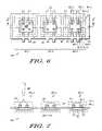
- FIG. 6shows a simplified plan view
- FIG. 7shows a simplified cut-away side view of a lead-frame with a semiconductor (SC) die, illustrating a buffer region being formed on the SC die prior to plastic encapsulation as in FIGS. 3-5 ; and
- SCsemiconductor
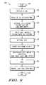
- FIG. 8shows a simplified flow chart illustrating a method according to a yet further embodiment of the present invention for forming a plastic encapsulated semiconductor (SC) device with lower package cross-talk and loss.
- SCplastic encapsulated semiconductor
- the term “lead-frame”is intended to include any supporting structure on which one or more individual or interconnected semiconductor die may be mounted, and may be metal, plastic ceramic, glass or combinations thereof.
- semiconductor dieand abbreviation “SC die” are intended to include semiconductor devices of any sort and configuration, whether individual devices or complex assemblies of devices such as in integrated circuits, or any other configuration of semiconductor devices.
- wire bondsand “bonding wires” are intended to include any means of electrically coupling package leads to contact regions and/or bonding pads on the SC die and not be limited merely to use of wires or the like. Non-limiting examples of other electrical coupling means are beam leads, solder bumps, metalized plastic tapes, and so forth.
- FIG. 3shows a simplified schematic cross-sectional view through molded plastic packaged device 40 containing semiconductor (SC) die 42 , according to a first embodiment of the present invention.
- Device 40comprises SC die or device 42 conveniently but not essentially mounted on heat sink 43 and surrounded (except perhaps for lower surface 41 of heat sink 43 ) by plastic encapsulation 47 .
- Plastic encapsulation 47may be such that lower surface 41 of heat sink 43 is exposed as indicated by outline 47 - 1 , or lower surface 41 may be embedded within plastic encapsulation 47 as indicated by outline 47 - 2 . Either arrangement for lower surface 41 is useful and not important to the present invention.
- buffer region 51having lower dielectric constant and/or lower loss tangent than encapsulation 47 .
- buffer region 51has lower dielectric constant than encapsulation 47 , the stray field capacitive coupling is reduced and performance enhanced.
- buffer region 51has lower loss tangent than encapsulation 47 , then stray field power loss is reduced and performance enhanced. While it is desirable that both the dielectric constant and the loss tangent of buffer region 51 be less than those of encapsulation 47 , this is not essential and improved performance can be obtained when either one is less than that of encapsulation 47 .
- Die 42has bonding or other connection pads or metalized regions 44 - 1 , 44 - 2 (collectively 44 ) on upper surface 50 of die 42 .
- Wire bonds or other connections 45 - 1 , 45 - 2(collectively 45 ) couple connection pads 44 to inner portions 48 - 1 , 48 - 2 (collectively 48 ) of external leads 46 - 1 , 46 - 2 (collectively 46 ), in order to provide external electrical coupling to die 42 .
- Elements 41 , 42 , 43 , 44 , 45 , 46 and 48are analogous in function to elements 21 , 22 , 23 , 24 , 25 , 26 and 28 of device 20 . Fringing electric field 49 of device 40 passes substantially through buffer region 51 .
- stray fringing electric field 49is shown in FIGS. 3-5 as extending between die bonding pads 44 - 1 , 44 - 2 having different electrical potential when device 40 is energized, this is merely for convenience of illustration and persons of skill in the art will understand that stray fringing fields can also extend above the surface of die 42 between other conductive regions, e.g., metal lines on die 42 (not shown), that receive different electrical potentials when used, and that all such stray fringing fields can contribute to the performance degradation described above that is mitigated by the present invention.
- Devices 40 and 20differ in that encapsulant 47 of device 40 is substantially not in contact with die 42 which, other than its lower surface where it is bonded to heat sink 43 , is enclosed in buffer region 51 .
- Region 51may be limited substantially to the immediate vicinity of die surface 50 (e.g., see FIG. 5 ) or may, as shown in FIGS. 3-4 , also enclose all or some parts of wire bonds or connections 45 and inner ends 48 of leads 46 . Either arrangement is useful.
- Buffer region 51needs to be chemically stable and electrically and chemically compatible with surface 50 of SC die 42 so as to not upset the operation of SC die 42 .
- FIG. 3illustrates the situation where buffer region 51 has therein, for example, a significant amount of filler 52 having a lower dielectric constant and/or loss tangent than binder or resin 53 that makes up the remainder of buffer region 51 . This has the effect of lowering the overall dielectric constant ⁇ and/or loss tangent ⁇ of region 51 relative to encapsulation 47 .
- buffer region 51be generally in contact with or in close proximity to device surface 50 , e.g., where metal pads or traces 44 are located, and also desirably but not essentially to wire bonds 45 and inner portions 48 of external leads 46 , so as to have the maximum beneficial effect of lowering the overall dielectric constant ⁇ and/or loss tangent ⁇ in these locations where fringing field 49 is strongest.
- a variety of low dielectric constant and/or low loss fillers 52are suitable for inclusion in buffer region 51 .
- filler 52should be chemically stable, compatible with binder resin 53 used in region 51 and the molding process, and available in a variety of generally microscopic sizes so as to facilitate a substantially uniform but generally random size distribution throughout region 51 . Further, it is desirable that adding filler 52 not result in a significant increase in the external porosity of region 51 or device 40 . It is desirable that a mix of filler sizes be used so that filler 52 can be tightly packed within binder resin 53 to fill as much space as possible (thereby minimizing the dielectric constant and/or loss tangent of the composite making up buffer region 51 ) with minimum impact on the overall package strength and hermeticity.
- Useful materialsare finely divided styrene and other light-weight plastics and glasses, and glass or ceramic fragments or hollow glass, ceramic or plastic microspheres, or combinations thereof.
- Hollow glass microspheresare a non-limiting example of a desirable filler material and are commercially available, for example, from the 3M Company of St. Paul, Minn. in a suitable range of sizes. It is desirable that the hollow microspheres or other low density particles have lower sizes of the order of typical device feature sizes (e.g., a few micrometers), and maximum sizes that are, for example, not larger than about 50% percent of thickness 54 of region 51 .
- the upper size limitis desirable to avoid having a fracture of one or more large microspheres cause an undesirable weak point or break in region 51 that might allow moisture to enter.
- the microspheres or other particlesbe about ⁇ 300 micro-meters, more conveniently about ⁇ 100 micro-meters and preferably about ⁇ 80 micro-meters in diameter or largest dimension.
- the microspheres or other filler particleshave a size range of usefully about 0.3 to 300 micro-meters, more conveniently about 3 to 100 micrometers and preferably about 3 to 80 micro-meters, but larger or smaller ranges can also be used, depending upon the particular devices being encapsulated, the size and construction of the lead-frame, the type of filler being used and so forth.
- the amount of hollow microspheres (or other filler) in the mixshould be as large as possible consistent with maintaining sufficient robustness and moisture resistance.
- the volume percentage of microspheres or other filler particles in region 51should be usefully equal or greater than about 50 volume percent, more conveniently equal or greater than about 60 volume percent and preferably equal or greater than about 70 volume percent in the mix or composite making up buffer region 51 .
- FIG. 4shows a simplified schematic cross-sectional view through molded plastic packaged device 60 containing semiconductor (SC) die 42 , according to a further embodiment of the present invention.
- Elements 41 , 42 , 43 , 44 , 45 , 46 , 47 , 47 - 1 , 47 - 2 and 48 of device 60are analogous to similarly identified elements in device 40 , and the description thereof in connection with device 40 is incorporated herein by reference.
- Devices 40 and 60differ in the constitution of buffer regions 51 , 61 around die 42 .
- Device 40illustrates the use of a low dielectric constant buffer region 51 containing filler 52 .
- Device 60illustrates the use of substantially homogeneous buffer region 61 providing a lower dielectric constant and/or lower loss tangent than encapsulation 47 .
- buffer region 61When buffer region 61 has lower dielectric constant than encapsulation 47 , the stray field capacitive coupling is reduced and performance enhanced. When buffer region 61 has lower loss tangent than encapsulation 47 , then stray field power loss is reduced and performance enhanced. While it is desirable that both the dielectric constant and the loss tangent of buffer region 61 be less than those of encapsulation 47 , this is not essential and improved performance can be obtained when either one is less than that of encapsulation 47 . Buffer region 61 needs to be chemically stable and electrically and chemically compatible with surface 50 of SC die 42 so as to not upset the operation of SC die 42 .
- suitable materialsare polyimide materials available from, Hitachi Company of Tokyo, Japan, Teflon® materials available from DuPont Corporation of Wilmington, Del. and SiLk® materials available from Dow Chemical Company of Midland, Mich.
- SOL-GELS and/or AERO-GELSare examples of useful materials. Such materials are generally commercially available and known in the art (e.g., see www.solgel.com). They can provide substantially inorganic or organic materials or combinations thereof for buffer region 51 , 61 , 71 , 81 .
- Device 60 of FIG. 4also illustrates use of optional sealing layer 62 covering buffer region 61 . While sealing layer 62 is illustrated only in FIG. 4 , it is also applicable to buffer region 51 of FIG. 3 , buffer region 71 of FIG. 5 and buffer region 81 of FIGS. 6-7 . Accordingly, as used herein, references to buffer region 61 in connection with sealing layer 62 are intended to include buffer regions 51 , 71 and 81 . Sealing layer 62 is desirable where buffer region 61 might introduce porosity within encapsulation 47 . Porosity that might permit easier ingress of moisture or other harmful substances is undesirable. Providing substantially impermeable sealing layer 62 over buffer region 61 can mitigate an increase in porosity introduced by region 61 .
- sealing layer 62Non-limiting examples of suitable materials for sealing layer 62 are: substantially inorganic materials such as deposited silicon dioxide and/or silicon nitride, substantially organic materials such as polyimide and/or parylene, and various combinations of inorganic and organic materials.
- sealing layer 62can be created in-situ by exposing buffer region 61 (or regions 51 , 71 and 81 ) to a plasma or other catalyst, for example, to promote cross-linking or other chemical reaction to render the surface layer of buffer region 61 (or 51 , 71 and 81 ) substantially impermeable to, for example, moisture.
- sealing layer 62is needed depends upon the choice of substances for buffer regions 51 , 61 , 71 and 81 and encapsulation 47 , the moisture sensitivity of die 42 and the environmental specifications that the finished encapsulated device is expected meet. These will vary from situation to situation and are within the competence of persons of skill in the art. Persons of skill in the art will understand how to decide whether sealing layer 62 is needed. While the use of sealing layer 62 is specifically illustrated in device 60 of FIG. 4 , such a sealing layer can also be used over buffer region 51 of device 40 of FIG. 3 , buffer region 71 of device 70 of FIG. 5 and buffer region 81 of FIGS. 6-7 , if desired. Further while barrier layer 62 is most useful in protecting against moisture incursion, it is not limited to this purpose and may also be used to retard or mitigate incursion of other harmful substances. Hence the term “sealing layer” is intended to include such functions.
- FIG. 5shows a simplified schematic cross-sectional view through molded plastic packaged device 70 containing semiconductor (SC) die 42 , according to a still further embodiment of the present invention.
- Elements 41 , 42 , 43 , 44 , 45 , 46 , 47 , 47 - 1 , 47 - 2 and 48 of device 70are analogous to similarly identified elements in devices 40 and 60 , and the description thereof in connection with devices 40 and 60 is incorporated herein by reference.
- Device 40 , 60 and 70differ in thickness 54 of buffer regions 51 , 61 and 71 . With devices 40 and 60 illustrated in FIGS.
- thickness 54is sufficient that buffer regions 51 , 61 not only cover die surface 50 but extend upward to substantially enclose wire bonds or other connections 45 and, optionally, part of end portions 48 of leads 46 .
- thickness 54is smaller so that buffer region 71 (analogous to regions 51 , 61 , with or without sealing layer 62 ) covers die surface 50 and die metallization 44 , but does not extend sufficiently to enclose all of wire bonds or connections 45 .
- the arrangement of FIG. 5is suitable where the die and package layout are such that fringing field 79 extends primarily between conductors and/or bonding pads on die surface 50 rather than between wire bonds 45 and lead portions 48 .
- buffer region 71is sufficient to reduce cross-talk and excessive dielectric loss in packaged device 70 .
- the same materialsmay be used for region 71 as for regions 51 , 61 , with or without overlying sealing layer 62 (see FIG. 4 ). Either arrangement is useful. Accordingly, the discussion of such materials in connection with FIGS. 3-4 is incorporated herein by reference.
- FIG. 6shows a simplified plan view
- FIG. 7shows a simplified cut-away side view of lead-frame 80 with SC die 42 , illustrating buffer region 81 analogous to regions 51 , 61 , 71 of FIGS. 3-5 being formed on and/or around SC die 42 prior to providing plastic encapsulation 47 .
- Elements 42 , 43 , 44 , 45 , 46 and 48 of FIGS. 6-7are analogous to similarly identified elements in FIGS. 3-5 .
- Three substantially representative sections 80 - 1 , 80 - 2 , 80 - 3are illustrated in lead-frame 80 , each carrying semiconductor die 42 , etc.
- Dashed outline 84indicates the approximate location of the mold cavity in which encapsulation 47 is to be formed around die 42 , heat sink 43 , bonding wires 45 , inner lead ends 48 , buffer region 81 , etc.
- lower surface 41 of die bonding flag 43will be enclosed in encapsulation 47 (see FIGS. 3-5 ), but this is not essential and it may be left exposed.
- Lead frame portions 82are trimmed away after forming encapsulation 47 so that, in this example, all that is left protruding from encapsulation 47 are leads 46 .
- Lead-frame sections 80 - 1 and 80 - 2illustrate buffer region 81 in place on portions 80 - 1 and 80 - 2 and having lower dielectric constant and/or lower loss tangent than subsequent encapsulation 47 .
- Buffer regions 81 on lead-frame sections 80 - 1 , 80 - 2are either cured or ready to be cured, depending upon the nature of the material making up buffer regions 81 , and ready to be enclosed in encapsulation 47 (see FIGS. 3-5 ).
- Lead-frame section 80 - 3illustrates buffer region 81 ′ just as it is being applied over die 42 , etc., from nozzle 86 . (Nozzle 86 is omitted from FIG. 6 in order to not obscure the view of underlying die 42 .) In this example in FIG.
- buffer region 81 ′has just been dispensed from nozzle 86 and dropped onto die 42 (and associated parts) where it will collapse to form region 81 shown in sections 80 - 2 and 80 - 1 .
- lead-frame 80By indexing lead-frame 80 in the direction shown by arrow 88 (or nozzle 86 in the opposite direction), each section 80 - 1 , 80 - 2 , 80 - 3 , . . . 80 -N of lead-frame 80 is brought under nozzle 86 so that buffer region 81 may be applied as desired.
- multiple nozzleseither in parallel or series
- multiple diemay be simultaneously coated with buffer region 81 , so that the process can be highly automated and inexpensively performed.
- sealing layere.g., analogous to layer 62 of FIG. 4
- itmay be applied over buffer region 81 in substantially the same manner, or sprayed on buffer region 81 , formed in situ or by any other convenient means, as has already been discussed.
- low dielectric constant buffer region 51 , 61 , 71 , 81has a dielectric constant that is usefully about ⁇ 80 percent of the dielectric constant of encapsulation 47 , more conveniently about ⁇ 60 percent and preferably about ⁇ 40 percent of encapsulation 47 .
- buffer region 51 , 61 , 71 , 81usefully has a relative dielectric constant of less than about 3.0, more conveniently less than about 2.5 and preferably less than about 2.0, and in any case less than the dielectric constant of encapsulation 47 .
- the loss tangent of buffer region 51 , 61 , 71 , 81is desirably less than about 0.005.
- FIG. 8show a simplified flow chart illustrating method 100 according to a yet further embodiment of the present invention for forming a plastic encapsulated semiconductor (SC) device with lower package cross-talk and/or loss, by providing buffer region 51 , 61 , 71 , 81 in the immediate vicinity of SC die 42 .
- Buffer region 51 , 61 , 71 , 81has a lower dielectric constant ⁇ and/or lower loss tangent ⁇ than surrounding encapsulation 47 , that is, lower ⁇ or lower ⁇ or both, which requirement is indicated on FIG.
- Method 100begins with START 102 and initial step 104 wherein one or more SC die 42 are provided.
- step 106die 42 are mounted on lead-frame 80 (as noted earlier, lead-frame 80 can be any type of support).
- step 108material having a lower dielectric constant ⁇ or lower loss tangent ⁇ or both relative to encapsulant 47 is dispensed onto die 42 and, optionally, also onto wirebonds 45 , inner leads 48 , etc.
- a seal coating(e.g., coating 62 of FIG. 4 ) may (or may not) be applied or formed depending upon the needs of the finished device.
- buffer region 51 , 61 , 71 , 81(and optional sealing layer 62 ) is cured if needed.
- the curing treatmentwill vary depending upon the type of material chosen for buffer region 51 , 61 , 71 , 81 (and optional sealing layer 62 ) and may include, for example and not intended to be limiting, a minimum elapsed time to allow a catalyzed resin to set up, or a heat treatment in the case of a thermosetting resin or a combination thereof or other cure process.
- buffer region 51 , 61 , 71 , 81may be cured before sealing layer 62 is applied or both may be cured together or sealing layer 62 may be cured separately.
- buffer region 51 , 61 , 71 , 81may be cured at the same time as encapsulation 47 in step 118 , depending upon the materials that have been chosen by the user. Persons of skill in the art will understand how to specify an appropriate cure regime depending upon the particular materials they have chosen.
- Optional cure step 112may be omitted or combined with any of following steps 114 , 116 and/or 118 , depending upon the cure required and the encapsulation conditions.
- lead-frame 80 with buffer region 51 , 61 , 71 , 81 appliedis inserted into a mold (not shown) having cavities indicated, for example, by dashed outline 84 in FIG.
- encapsulant 47is applied over low ⁇ and/or ⁇ buffer region 51 , 61 , 71 , 81 and the inner lead-frame parts not already covered by region 51 , 61 , 71 , 81 .
- encapsulant 47is appropriately cured using means well known in the art.
- the encapsulated lead-frameis removed from the mold.
- Method 100proceeds to END 122 .
- Subsequent processinge.g., trim, lead-form, test, etc. is conventional.
- a semiconductor devicecomprising, a supporting member, a semiconductor die mounted on a portion of the supporting member, a plastic encapsulation enclosing at least part of the supporting member and the die, and a buffer region located between the plastic encapsulation and the die, wherein the buffer region has a lower dielectric constant than the plastic encapsulation or a lower loss tangent than the plastic encapsulation or both.
- the buffer regioncomprises hollow microspheres in a binder matrix.
- the hollow microspheresare hollow glass microspheres having sizes about ⁇ 300 micrometers in diameter.
- the buffer regionhas a relative dielectric constant about ⁇ 3.
- the buffer regionhas a loss tangent about ⁇ 0.005.
- a plastic encapsulated semiconductor devicecomprising, a semiconductor die having one or more bonding pads thereon, a plastic encapsulation surrounding one or more faces of the semiconductor die, and a buffer region located between the plastic encapsulation and the semiconductor die and including at least one of the one or more bonding pads, wherein the buffer region has a lower dielectric constant than the plastic encapsulation or a lower loss tangent than the plastic encapsulation or both.
- the buffer regionis in contact with the one or more faces of the semiconductor die.
- the buffer regionincludes a filler.
- the fillercomprises hollow microspheres less than about 300 micro-meters in diameter.
- the buffer regioncomprises a material having a dielectric constant less than or equal about 80% of the dielectric constant of the plastic encapsulation. In a yet still additional embodiment, the buffer region comprises a porous material. In a still yet further embodiment, the device further comprising a moisture sealing layer located between the buffer region and the plastic encapsulation
- a method of encapsulating a semiconductor diecomprising, mounting the die on a lead-frame, covering a portion of the die with a buffer region of a first dielectric constant and first loss tangent, placing the lead-frame with the die and buffer region in a mold suitable for plastic encapsulation, wherein the die and buffer region are located in a cavity in the mold, and placing a plastic encapsulant in the cavity of the mold to substantially fill the cavity of the mold around the lead frame, die and buffer region with a plastic material of a second dielectric constant and a second loss tangent, wherein either the second dielectric constant is larger than the first dielectric constant or the second loss tangent is larger than the first loss tangent.
- the methodfurther comprises, after the covering step, at least partly curing the buffer region.
- the covering stepcomprises covering a portion of the die with a buffer region material having a filler therein comprising hollow microspheres.
- the covering stepcomprises covering a portion of the die with a buffer region material having a first dielectric constant less than about 80% of the second dielectric constant.
- the methodcomprises, between the covering step and the placing step, covering the buffer region with a sealing layer.
- the covering stepcomprises covering a portion of the die with a substantially organic material.
- the covering stepcomprises, covering a portion of the die with a substantially inorganic material.
Landscapes
- Physics & Mathematics (AREA)
- Condensed Matter Physics & Semiconductors (AREA)
- General Physics & Mathematics (AREA)
- Engineering & Computer Science (AREA)
- Computer Hardware Design (AREA)
- Microelectronics & Electronic Packaging (AREA)
- Power Engineering (AREA)
- Structures Or Materials For Encapsulating Or Coating Semiconductor Devices Or Solid State Devices (AREA)
- Encapsulation Of And Coatings For Semiconductor Or Solid State Devices (AREA)
Abstract
Description
Claims (12)
Priority Applications (6)
| Application Number | Priority Date | Filing Date | Title |
|---|---|---|---|
| US11/257,802US7435625B2 (en) | 2005-10-24 | 2005-10-24 | Semiconductor device with reduced package cross-talk and loss |
| JP2008536797AJP2009513019A (en) | 2005-10-24 | 2006-10-18 | Semiconductor device with reduced package crosstalk and loss |
| KR1020087009842AKR101296701B1 (en) | 2005-10-24 | 2006-10-18 | Semiconductor device with reduced package cross-talk and loss |
| PCT/US2006/040869WO2007050420A2 (en) | 2005-10-24 | 2006-10-18 | Semiconductor device with reduced package cross-talk and loss |
| TW095139041ATWI414046B (en) | 2005-10-24 | 2006-10-23 | Semiconductor device with reduced package cross-talk and loss |
| US12/204,500US7701074B2 (en) | 2005-10-24 | 2008-09-04 | Semiconductor device with a buffer region with tightly-packed filler particles |
Applications Claiming Priority (1)
| Application Number | Priority Date | Filing Date | Title |
|---|---|---|---|
| US11/257,802US7435625B2 (en) | 2005-10-24 | 2005-10-24 | Semiconductor device with reduced package cross-talk and loss |
Related Child Applications (1)
| Application Number | Title | Priority Date | Filing Date |
|---|---|---|---|
| US12/204,500DivisionUS7701074B2 (en) | 2005-10-24 | 2008-09-04 | Semiconductor device with a buffer region with tightly-packed filler particles |
Publications (2)
| Publication Number | Publication Date |
|---|---|
| US20070090542A1 US20070090542A1 (en) | 2007-04-26 |
| US7435625B2true US7435625B2 (en) | 2008-10-14 |
Family
ID=37968396
Family Applications (2)
| Application Number | Title | Priority Date | Filing Date |
|---|---|---|---|
| US11/257,802Active2025-11-01US7435625B2 (en) | 2005-10-24 | 2005-10-24 | Semiconductor device with reduced package cross-talk and loss |
| US12/204,500Expired - Fee RelatedUS7701074B2 (en) | 2005-10-24 | 2008-09-04 | Semiconductor device with a buffer region with tightly-packed filler particles |
Family Applications After (1)
| Application Number | Title | Priority Date | Filing Date |
|---|---|---|---|
| US12/204,500Expired - Fee RelatedUS7701074B2 (en) | 2005-10-24 | 2008-09-04 | Semiconductor device with a buffer region with tightly-packed filler particles |
Country Status (5)
| Country | Link |
|---|---|
| US (2) | US7435625B2 (en) |
| JP (1) | JP2009513019A (en) |
| KR (1) | KR101296701B1 (en) |
| TW (1) | TWI414046B (en) |
| WO (1) | WO2007050420A2 (en) |
Cited By (7)
| Publication number | Priority date | Publication date | Assignee | Title |
|---|---|---|---|---|
| US20080259585A1 (en)* | 2006-09-27 | 2008-10-23 | Shinko Electric Industries Co., Ltd. | Electronic apparatus |
| US20110318887A1 (en)* | 2010-06-28 | 2011-12-29 | Samsung Electronics Co., Ltd. | Method of molding semiconductor package |
| US20140103508A1 (en)* | 2012-10-11 | 2014-04-17 | Texas Instruments Incorporated | Encapsulating package for an integrated circuit |
| US20190132959A1 (en)* | 2017-10-30 | 2019-05-02 | Baker Hughes, A Ge Company, Llc | Encapsulation of downhole microelectronics |
| US10446414B2 (en)* | 2017-12-22 | 2019-10-15 | Texas Instruments Incorporated | Semiconductor package with filler particles in a mold compound |
| US10672703B2 (en) | 2018-09-26 | 2020-06-02 | Nxp Usa, Inc. | Transistor with shield structure, packaged device, and method of fabrication |
| KR20200081366A (en)* | 2017-10-31 | 2020-07-07 | 나가세케무텍쿠스가부시키가이샤 | Manufacturing method of mounting structure and sheet used therefor |
Families Citing this family (15)
| Publication number | Priority date | Publication date | Assignee | Title |
|---|---|---|---|---|
| DE102009026804A1 (en)* | 2009-06-08 | 2010-12-09 | Robert Bosch Gmbh | Method for producing electronic components |
| JP5018909B2 (en)* | 2009-06-30 | 2012-09-05 | 株式会社デンソー | Semiconductor device |
| JP2011054806A (en)* | 2009-09-02 | 2011-03-17 | Renesas Electronics Corp | Semiconductor device and method of manufacturing the same |
| CN102714556B (en)* | 2010-04-28 | 2016-05-25 | 华为技术有限公司 | Crosstalking in bi-directional light electronic equipment reduces |
| JP5532419B2 (en)* | 2010-06-17 | 2014-06-25 | 富士電機株式会社 | Insulating material, metal base substrate, semiconductor module, and manufacturing method thereof |
| CN102714542B (en)* | 2010-06-25 | 2015-08-19 | Hoya美国公司 | Crosstalk in bidirectional optoelectronic device reduces |
| CN102714555B (en)* | 2010-09-06 | 2016-06-15 | 华为技术有限公司 | Crosstalk in bidirectional optoelectronic device reduces |
| CN103858035A (en) | 2011-10-28 | 2014-06-11 | Hoya美国公司 | Optical waveguide splitter on a waveguide substrate for attenuating a light source |
| US9490041B2 (en) | 2012-03-27 | 2016-11-08 | 3M Innovative Properties Company | Composite particles comprising a conductive coating of PEDOT/PSS, methods of making, and articles including the same |
| KR101905893B1 (en)* | 2012-06-13 | 2018-10-08 | 에스케이하이닉스 주식회사 | Embedded package including multilayered dielectric and method for manufacturing the same |
| US9226428B2 (en)* | 2012-06-28 | 2015-12-29 | Intel Corporation | High heat capacity electronic components and methods for fabricating |
| EP2731130A1 (en)* | 2012-11-12 | 2014-05-14 | Nxp B.V. | Cavity package for an integrated circuit |
| US9312231B2 (en)* | 2013-10-31 | 2016-04-12 | Freescale Semiconductor, Inc. | Method and apparatus for high temperature semiconductor device packages and structures using a low temperature process |
| US9461005B2 (en)* | 2015-02-12 | 2016-10-04 | Ampleon Netherlands B.V. | RF package with non-gaseous dielectric material |
| US10431526B2 (en)* | 2017-10-09 | 2019-10-01 | Cree, Inc. | Rivetless lead fastening for a semiconductor package |
Citations (29)
| Publication number | Priority date | Publication date | Assignee | Title |
|---|---|---|---|---|
| US4041009A (en)* | 1976-12-08 | 1977-08-09 | Fujitsu Limited | Process for producing anti-blocking and low pressure moldable diallyl phthalate resin molding materials |
| US4079162A (en)* | 1974-03-20 | 1978-03-14 | Aim Associates, Inc. | Soundproof structure |
| US4788583A (en)* | 1986-07-25 | 1988-11-29 | Fujitsu Limited | Semiconductor device and method of producing semiconductor device |
| US5057457A (en)* | 1989-09-13 | 1991-10-15 | Kabushiki Kaisha Toshiba | Multimold semiconductor device and the manufacturing method therefor |
| US5097317A (en)* | 1989-09-08 | 1992-03-17 | Mitsubishi Denki Kabushiki Kaisha | Resin-sealed semiconductor device |
| US5379186A (en)* | 1993-07-06 | 1995-01-03 | Motorola, Inc. | Encapsulated electronic component having a heat diffusing layer |
| US5382829A (en)* | 1992-07-21 | 1995-01-17 | Mitsubishi Denki Kabushiki Kaisha | Packaged microwave semiconductor device |
| US5446315A (en)* | 1991-03-08 | 1995-08-29 | Japan Gore-Tex, Inc. | Resin-sealed semiconductor device containing porous fluorocarbon resin |
| US5458709A (en) | 1991-04-12 | 1995-10-17 | Fujitsu Limited | Process for manufacturing multi-layer glass ceramic substrate |
| US5578860A (en) | 1995-05-01 | 1996-11-26 | Motorola, Inc. | Monolithic high frequency integrated circuit structure having a grounded source configuration |
| US5593526A (en) | 1990-09-20 | 1997-01-14 | Fujitsu Limited | Process for preparing a multi-layer wiring board |
| US5598034A (en) | 1992-07-22 | 1997-01-28 | Vlsi Packaging Corporation | Plastic packaging of microelectronic circuit devices |
| JPH0927573A (en)* | 1995-07-13 | 1997-01-28 | Mitsubishi Electric Corp | Semiconductor device |
| US5785789A (en)* | 1993-03-18 | 1998-07-28 | Digital Equipment Corporation | Low dielectric constant microsphere filled layers for multilayer electrical structures |
| US5793118A (en)* | 1994-05-26 | 1998-08-11 | Nec Corporation | Semiconductor device capable of accomplishing a high moisture proof |
| US5869355A (en)* | 1996-06-11 | 1999-02-09 | Yamaha Corp. | Lead frame with increased strength and manufacture of semiconductor device |
| US5889232A (en)* | 1996-05-14 | 1999-03-30 | Nec Corporation | Ultrahigh-frequency electronic component |
| US6001673A (en) | 1999-02-11 | 1999-12-14 | Ericsson Inc. | Methods for packaging integrated circuit devices including cavities adjacent active regions |
| US6191492B1 (en)* | 1988-08-26 | 2001-02-20 | Semiconductor Energy Laboratory Co., Ltd. | Electronic device including a densified region |
| US20020033108A1 (en)* | 2000-04-07 | 2002-03-21 | Keiji Akiyama | Heat-sensitive lithographic printing plate precursor |
| US6440772B1 (en)* | 1999-12-06 | 2002-08-27 | Micron Technology, Inc. | Bow resistant plastic semiconductor package and method of fabrication |
| US6455606B1 (en)* | 1997-04-02 | 2002-09-24 | Sanyo Chemical Industries, Ltd. | Polyurethane foam, process for producing the same, and foam forming composition |
| US6521703B2 (en)* | 2000-01-18 | 2003-02-18 | General Electric Company | Curable resin composition, method for the preparation thereof, and articles derived thereform |
| US20030130438A1 (en)* | 2001-06-28 | 2003-07-10 | Akikazu Amagai | Bifunctional phenylene ether oligomer, its derivatives its use and process for the production thereof |
| US6630153B2 (en)* | 2001-02-23 | 2003-10-07 | Smith & Nephew, Inc. | Manufacture of bone graft substitutes |
| US6713590B2 (en) | 2000-07-19 | 2004-03-30 | Honeywell International Inc. | Low dielectric constant materials with polymeric networks |
| US6744117B2 (en) | 2002-02-28 | 2004-06-01 | Motorola, Inc. | High frequency semiconductor device and method of manufacture |
| US6849696B2 (en) | 2000-04-07 | 2005-02-01 | Honeywell International Inc. | Low dielectric constant organic dielectrics based on cage-like structures |
| US6890641B1 (en) | 2002-07-03 | 2005-05-10 | Honeywell International Inc. | Low dielectric materials and methods of producing same |
Family Cites Families (3)
| Publication number | Priority date | Publication date | Assignee | Title |
|---|---|---|---|---|
| JPS6379353A (en)* | 1986-09-24 | 1988-04-09 | Hitachi Ltd | Resin-sealed semiconductor device |
| JP2988117B2 (en)* | 1992-03-30 | 1999-12-06 | 日本電気株式会社 | Resin-sealed semiconductor device |
| TWI457835B (en)* | 2004-02-04 | 2014-10-21 | Semiconductor Energy Lab | An article carrying a thin flim integrated circuit |
- 2005
- 2005-10-24USUS11/257,802patent/US7435625B2/enactiveActive
- 2006
- 2006-10-18JPJP2008536797Apatent/JP2009513019A/enactivePending
- 2006-10-18WOPCT/US2006/040869patent/WO2007050420A2/enactiveApplication Filing
- 2006-10-18KRKR1020087009842Apatent/KR101296701B1/ennot_activeExpired - Fee Related
- 2006-10-23TWTW095139041Apatent/TWI414046B/ennot_activeIP Right Cessation
- 2008
- 2008-09-04USUS12/204,500patent/US7701074B2/ennot_activeExpired - Fee Related
Patent Citations (30)
| Publication number | Priority date | Publication date | Assignee | Title |
|---|---|---|---|---|
| US4079162A (en)* | 1974-03-20 | 1978-03-14 | Aim Associates, Inc. | Soundproof structure |
| US4041009A (en)* | 1976-12-08 | 1977-08-09 | Fujitsu Limited | Process for producing anti-blocking and low pressure moldable diallyl phthalate resin molding materials |
| US4788583A (en)* | 1986-07-25 | 1988-11-29 | Fujitsu Limited | Semiconductor device and method of producing semiconductor device |
| US6191492B1 (en)* | 1988-08-26 | 2001-02-20 | Semiconductor Energy Laboratory Co., Ltd. | Electronic device including a densified region |
| US5097317A (en)* | 1989-09-08 | 1992-03-17 | Mitsubishi Denki Kabushiki Kaisha | Resin-sealed semiconductor device |
| US5057457A (en)* | 1989-09-13 | 1991-10-15 | Kabushiki Kaisha Toshiba | Multimold semiconductor device and the manufacturing method therefor |
| US5593526A (en) | 1990-09-20 | 1997-01-14 | Fujitsu Limited | Process for preparing a multi-layer wiring board |
| US5446315A (en)* | 1991-03-08 | 1995-08-29 | Japan Gore-Tex, Inc. | Resin-sealed semiconductor device containing porous fluorocarbon resin |
| US5458709A (en) | 1991-04-12 | 1995-10-17 | Fujitsu Limited | Process for manufacturing multi-layer glass ceramic substrate |
| US5382829A (en)* | 1992-07-21 | 1995-01-17 | Mitsubishi Denki Kabushiki Kaisha | Packaged microwave semiconductor device |
| US5598034A (en) | 1992-07-22 | 1997-01-28 | Vlsi Packaging Corporation | Plastic packaging of microelectronic circuit devices |
| US5785789A (en)* | 1993-03-18 | 1998-07-28 | Digital Equipment Corporation | Low dielectric constant microsphere filled layers for multilayer electrical structures |
| US5379186A (en)* | 1993-07-06 | 1995-01-03 | Motorola, Inc. | Encapsulated electronic component having a heat diffusing layer |
| US5793118A (en)* | 1994-05-26 | 1998-08-11 | Nec Corporation | Semiconductor device capable of accomplishing a high moisture proof |
| US5578860A (en) | 1995-05-01 | 1996-11-26 | Motorola, Inc. | Monolithic high frequency integrated circuit structure having a grounded source configuration |
| JPH0927573A (en)* | 1995-07-13 | 1997-01-28 | Mitsubishi Electric Corp | Semiconductor device |
| US5889232A (en)* | 1996-05-14 | 1999-03-30 | Nec Corporation | Ultrahigh-frequency electronic component |
| US5869355A (en)* | 1996-06-11 | 1999-02-09 | Yamaha Corp. | Lead frame with increased strength and manufacture of semiconductor device |
| US6455606B1 (en)* | 1997-04-02 | 2002-09-24 | Sanyo Chemical Industries, Ltd. | Polyurethane foam, process for producing the same, and foam forming composition |
| US6001673A (en) | 1999-02-11 | 1999-12-14 | Ericsson Inc. | Methods for packaging integrated circuit devices including cavities adjacent active regions |
| US6440772B1 (en)* | 1999-12-06 | 2002-08-27 | Micron Technology, Inc. | Bow resistant plastic semiconductor package and method of fabrication |
| US6521703B2 (en)* | 2000-01-18 | 2003-02-18 | General Electric Company | Curable resin composition, method for the preparation thereof, and articles derived thereform |
| US20020033108A1 (en)* | 2000-04-07 | 2002-03-21 | Keiji Akiyama | Heat-sensitive lithographic printing plate precursor |
| US6849696B2 (en) | 2000-04-07 | 2005-02-01 | Honeywell International Inc. | Low dielectric constant organic dielectrics based on cage-like structures |
| US6713590B2 (en) | 2000-07-19 | 2004-03-30 | Honeywell International Inc. | Low dielectric constant materials with polymeric networks |
| US6630153B2 (en)* | 2001-02-23 | 2003-10-07 | Smith & Nephew, Inc. | Manufacture of bone graft substitutes |
| US20030130438A1 (en)* | 2001-06-28 | 2003-07-10 | Akikazu Amagai | Bifunctional phenylene ether oligomer, its derivatives its use and process for the production thereof |
| US6794481B2 (en) | 2001-06-28 | 2004-09-21 | Mitsubishi Gas Chemical Company, Inc. | Bifunctional phenylene ether oligomer, its derivatives, its use and process for the production thereof |
| US6744117B2 (en) | 2002-02-28 | 2004-06-01 | Motorola, Inc. | High frequency semiconductor device and method of manufacture |
| US6890641B1 (en) | 2002-07-03 | 2005-05-10 | Honeywell International Inc. | Low dielectric materials and methods of producing same |
Non-Patent Citations (10)
| Title |
|---|
| Dow Unveils Advanced SiLK Resin Featuring Drastically Smaller Pore Size, Introduces First Porous ILD to Enable Continuous Tantalum Barriers, Dow Chemical Company, Dec. 25, 2003, http://www.dow.com/silk/news/20030918b.htm. |
| International Search Report and Written Opinion. |
| Perry, J. et al., SiLK Semiconductor Dielectric Resins, technical paper, Dow Chemical Company, pp. 1-6. |
| Peters, Laura, Is Pore Sealing Key to Ultralow-k Adoption?, Semiconductor International, Oct. 1, 2005, http://www.reed-electronics.com/semiconductor/article/CA6260716?industryid=3032&nid=2012. |
| Phalippou, Jean, Sol-Gel: A Low Temperature Process for the Materials of the New Millenium, Sol-Gel Tutorial, http://www.solgel.com/articles/June00/phalip/introsolgel.htm. |
| Physical Sciences-Sol Gel Introduction, http://www.bell-labs.com/org/physicalsciences/projects/solgel/solgel.html. |
| Prassas, Michael, Silica Glass from Aerogels, Sol-Gel Gateway: Glass from Aerogels, http://www.solgel.com/articles/april01/aerog2.htm and http://www.solgel.com/articles/april01.aerog.htm. |
| SiLK Works, Dow Chemical Company, http://www.dow.com/silk/index.htm. |
| Simmonds, M. et al., SiLK Semiconductor Dielectric Resin Films, technical paper, Dow Chemical Company, pp. 1-7. |
| Sol-Gel Technologies, Sol-Gel Improves the quality of Human Life, http://www.sol-gel.com/technology.html. |
Cited By (14)
| Publication number | Priority date | Publication date | Assignee | Title |
|---|---|---|---|---|
| US8094457B2 (en)* | 2006-09-27 | 2012-01-10 | Shinko Electric Industries Co., Ltd. | Electronic apparatus |
| US20080259585A1 (en)* | 2006-09-27 | 2008-10-23 | Shinko Electric Industries Co., Ltd. | Electronic apparatus |
| US9184065B2 (en) | 2010-06-28 | 2015-11-10 | Samsung Electronics Co., Ltd. | Method of molding semiconductor package |
| US8420450B2 (en)* | 2010-06-28 | 2013-04-16 | Samsung Electronics Co., Ltd. | Method of molding semiconductor package |
| US8956921B2 (en) | 2010-06-28 | 2015-02-17 | Samsung Electronics Co., Ltd. | Method of molding semiconductor package |
| US20110318887A1 (en)* | 2010-06-28 | 2011-12-29 | Samsung Electronics Co., Ltd. | Method of molding semiconductor package |
| US20140103508A1 (en)* | 2012-10-11 | 2014-04-17 | Texas Instruments Incorporated | Encapsulating package for an integrated circuit |
| US20190132959A1 (en)* | 2017-10-30 | 2019-05-02 | Baker Hughes, A Ge Company, Llc | Encapsulation of downhole microelectronics |
| US10897824B2 (en)* | 2017-10-30 | 2021-01-19 | Baker Hughes, A Ge Company, Llc | Encapsulation of downhole microelectronics and method the same |
| KR20200081366A (en)* | 2017-10-31 | 2020-07-07 | 나가세케무텍쿠스가부시키가이샤 | Manufacturing method of mounting structure and sheet used therefor |
| US11410898B2 (en)* | 2017-10-31 | 2022-08-09 | Nagase Chemtex Corporation | Manufacturing method of mounting structure, and sheet therefor |
| TWI785138B (en)* | 2017-10-31 | 2022-12-01 | 日商長瀨化成股份有限公司 | Manufacturing method of mounting structure and sheet used therefor |
| US10446414B2 (en)* | 2017-12-22 | 2019-10-15 | Texas Instruments Incorporated | Semiconductor package with filler particles in a mold compound |
| US10672703B2 (en) | 2018-09-26 | 2020-06-02 | Nxp Usa, Inc. | Transistor with shield structure, packaged device, and method of fabrication |
Also Published As
| Publication number | Publication date |
|---|---|
| KR20080065980A (en) | 2008-07-15 |
| JP2009513019A (en) | 2009-03-26 |
| US20070090542A1 (en) | 2007-04-26 |
| TW200729427A (en) | 2007-08-01 |
| US7701074B2 (en) | 2010-04-20 |
| WO2007050420A2 (en) | 2007-05-03 |
| WO2007050420A3 (en) | 2007-08-30 |
| TWI414046B (en) | 2013-11-01 |
| US20090001614A1 (en) | 2009-01-01 |
| KR101296701B1 (en) | 2013-08-20 |
Similar Documents
| Publication | Publication Date | Title |
|---|---|---|
| US7701074B2 (en) | Semiconductor device with a buffer region with tightly-packed filler particles | |
| US7361987B2 (en) | Circuit device with at least partial packaging and method for forming | |
| WO2007050421A2 (en) | Semiconductor device with improved encapsulation | |
| KR101418397B1 (en) | Semiconductor package and manufacturing method thereof | |
| CN101517718B (en) | Plastic packaged device with die interface layer | |
| CN107265393B (en) | Semiconductor Devices Containing MEMS Dies | |
| CN102610533B (en) | Injection sealing system and method thereof | |
| US7868430B2 (en) | Semiconductor device | |
| CN111201597A (en) | Rivetless lead fastening for semiconductor packages | |
| US6818968B1 (en) | Integrated circuit package and process for forming the same | |
| CN112864047A (en) | Semiconductor device with package-level zoning shield and associated systems and methods | |
| CN101226927B (en) | Chip module with power amplifier and manufacturing method thereof | |
| US9230874B1 (en) | Integrated circuit package with a heat conductor | |
| JP2006086337A (en) | Resin-sealed electronic device and manufacturing method thereof | |
| US20020177254A1 (en) | Semiconductor package and method for making the same | |
| KR101135828B1 (en) | Flip chip mlp with conductive ink | |
| KR101494371B1 (en) | Semiconductor package with different type substrates | |
| US20240153885A1 (en) | Semiconductor devices with electrical insulation features and associated production methods | |
| CN120511235A (en) | Semiconductor module arrangement, electronics carrier for a semiconductor module arrangement, and method for producing a semiconductor module arrangement | |
| KR100991226B1 (en) | Chip package assembly having a metal cap and a method of manufacturing the same | |
| CN101393948B (en) | Front and back clamping type light emitting diode packaging structure and packaging method thereof | |
| KR100992450B1 (en) | Multilayer chip package | |
| US8980690B1 (en) | Lead frame based semiconductor device with routing substrate | |
| KR101983164B1 (en) | Power Semi-Conductor package and Method of Manufacturing for the same | |
| CN103579135A (en) | Semiconductor package, manufacturing method thereof, and semiconductor package manufacturing mold |
Legal Events
| Date | Code | Title | Description |
|---|---|---|---|
| AS | Assignment | Owner name:FREESCALE SEMICONDUCTOR, INC., TEXAS Free format text:ASSIGNMENT OF ASSIGNORS INTEREST;ASSIGNORS:CONDIE, BRIAN W.;MAHALINGAM, L.M.;SHAH, MAHESH K.;REEL/FRAME:017147/0754 Effective date:20051011 | |
| AS | Assignment | Owner name:CITIBANK, N.A. AS COLLATERAL AGENT, NEW YORK Free format text:SECURITY AGREEMENT;ASSIGNORS:FREESCALE SEMICONDUCTOR, INC.;FREESCALE ACQUISITION CORPORATION;FREESCALE ACQUISITION HOLDINGS CORP.;AND OTHERS;REEL/FRAME:018855/0129 Effective date:20061201 Owner name:CITIBANK, N.A. AS COLLATERAL AGENT,NEW YORK Free format text:SECURITY AGREEMENT;ASSIGNORS:FREESCALE SEMICONDUCTOR, INC.;FREESCALE ACQUISITION CORPORATION;FREESCALE ACQUISITION HOLDINGS CORP.;AND OTHERS;REEL/FRAME:018855/0129 Effective date:20061201 | |
| FEPP | Fee payment procedure | Free format text:PAYOR NUMBER ASSIGNED (ORIGINAL EVENT CODE: ASPN); ENTITY STATUS OF PATENT OWNER: LARGE ENTITY | |
| STCF | Information on status: patent grant | Free format text:PATENTED CASE | |
| AS | Assignment | Owner name:CITIBANK, N.A., NEW YORK Free format text:SECURITY AGREEMENT;ASSIGNOR:FREESCALE SEMICONDUCTOR, INC.;REEL/FRAME:022380/0409 Effective date:20090216 Owner name:CITIBANK, N.A.,NEW YORK Free format text:SECURITY AGREEMENT;ASSIGNOR:FREESCALE SEMICONDUCTOR, INC.;REEL/FRAME:022380/0409 Effective date:20090216 | |
| AS | Assignment | Owner name:CITIBANK, N.A., AS COLLATERAL AGENT,NEW YORK Free format text:SECURITY AGREEMENT;ASSIGNOR:FREESCALE SEMICONDUCTOR, INC.;REEL/FRAME:024397/0001 Effective date:20100413 Owner name:CITIBANK, N.A., AS COLLATERAL AGENT, NEW YORK Free format text:SECURITY AGREEMENT;ASSIGNOR:FREESCALE SEMICONDUCTOR, INC.;REEL/FRAME:024397/0001 Effective date:20100413 | |
| FPAY | Fee payment | Year of fee payment:4 | |
| AS | Assignment | Owner name:CITIBANK, N.A., AS NOTES COLLATERAL AGENT, NEW YORK Free format text:SECURITY AGREEMENT;ASSIGNOR:FREESCALE SEMICONDUCTOR, INC.;REEL/FRAME:030633/0424 Effective date:20130521 Owner name:CITIBANK, N.A., AS NOTES COLLATERAL AGENT, NEW YOR Free format text:SECURITY AGREEMENT;ASSIGNOR:FREESCALE SEMICONDUCTOR, INC.;REEL/FRAME:030633/0424 Effective date:20130521 | |
| AS | Assignment | Owner name:CITIBANK, N.A., AS NOTES COLLATERAL AGENT, NEW YORK Free format text:SECURITY AGREEMENT;ASSIGNOR:FREESCALE SEMICONDUCTOR, INC.;REEL/FRAME:031591/0266 Effective date:20131101 Owner name:CITIBANK, N.A., AS NOTES COLLATERAL AGENT, NEW YOR Free format text:SECURITY AGREEMENT;ASSIGNOR:FREESCALE SEMICONDUCTOR, INC.;REEL/FRAME:031591/0266 Effective date:20131101 | |
| AS | Assignment | Owner name:FREESCALE SEMICONDUCTOR, INC., TEXAS Free format text:PATENT RELEASE;ASSIGNOR:CITIBANK, N.A., AS COLLATERAL AGENT;REEL/FRAME:037354/0225 Effective date:20151207 Owner name:FREESCALE SEMICONDUCTOR, INC., TEXAS Free format text:PATENT RELEASE;ASSIGNOR:CITIBANK, N.A., AS COLLATERAL AGENT;REEL/FRAME:037354/0807 Effective date:20151207 Owner name:FREESCALE SEMICONDUCTOR, INC., TEXAS Free format text:PATENT RELEASE;ASSIGNOR:CITIBANK, N.A., AS COLLATERAL AGENT;REEL/FRAME:037356/0553 Effective date:20151207 Owner name:FREESCALE SEMICONDUCTOR, INC., TEXAS Free format text:PATENT RELEASE;ASSIGNOR:CITIBANK, N.A., AS COLLATERAL AGENT;REEL/FRAME:037356/0143 Effective date:20151207 | |
| AS | Assignment | Owner name:MORGAN STANLEY SENIOR FUNDING, INC., MARYLAND Free format text:ASSIGNMENT AND ASSUMPTION OF SECURITY INTEREST IN PATENTS;ASSIGNOR:CITIBANK, N.A.;REEL/FRAME:037486/0517 Effective date:20151207 | |
| AS | Assignment | Owner name:MORGAN STANLEY SENIOR FUNDING, INC., MARYLAND Free format text:ASSIGNMENT AND ASSUMPTION OF SECURITY INTEREST IN PATENTS;ASSIGNOR:CITIBANK, N.A.;REEL/FRAME:037518/0292 Effective date:20151207 | |
| AS | Assignment | Owner name:NORTH STAR INNOVATIONS INC., CALIFORNIA Free format text:ASSIGNMENT OF ASSIGNORS INTEREST;ASSIGNOR:FREESCALE SEMICONDUCTOR, INC.;REEL/FRAME:037694/0264 Effective date:20151002 | |
| REMI | Maintenance fee reminder mailed | ||
| AS | Assignment | Owner name:NXP, B.V., F/K/A FREESCALE SEMICONDUCTOR, INC., NETHERLANDS Free format text:RELEASE BY SECURED PARTY;ASSIGNOR:MORGAN STANLEY SENIOR FUNDING, INC.;REEL/FRAME:040925/0001 Effective date:20160912 Owner name:NXP, B.V., F/K/A FREESCALE SEMICONDUCTOR, INC., NE Free format text:RELEASE BY SECURED PARTY;ASSIGNOR:MORGAN STANLEY SENIOR FUNDING, INC.;REEL/FRAME:040925/0001 Effective date:20160912 | |
| FPAY | Fee payment | Year of fee payment:8 | |
| SULP | Surcharge for late payment | Year of fee payment:7 | |
| AS | Assignment | Owner name:NXP B.V., NETHERLANDS Free format text:RELEASE BY SECURED PARTY;ASSIGNOR:MORGAN STANLEY SENIOR FUNDING, INC.;REEL/FRAME:040928/0001 Effective date:20160622 | |
| AS | Assignment | Owner name:MORGAN STANLEY SENIOR FUNDING, INC., MARYLAND Free format text:CORRECTIVE ASSIGNMENT TO CORRECT THE REMOVE PATENTS 8108266 AND 8062324 AND REPLACE THEM WITH 6108266 AND 8060324 PREVIOUSLY RECORDED ON REEL 037518 FRAME 0292. ASSIGNOR(S) HEREBY CONFIRMS THE ASSIGNMENT AND ASSUMPTION OF SECURITY INTEREST IN PATENTS;ASSIGNOR:CITIBANK, N.A.;REEL/FRAME:041703/0536 Effective date:20151207 | |
| AS | Assignment | Owner name:TAIWAN SEMICONDUCTOR MANUFACTURING CO., LTD., TAIW Free format text:ASSIGNMENT OF ASSIGNORS INTEREST;ASSIGNOR:NORTH STAR INNOVATIONS INC.;REEL/FRAME:041717/0736 Effective date:20161006 | |
| AS | Assignment | Owner name:SHENZHEN XINGUODU TECHNOLOGY CO., LTD., CHINA Free format text:CORRECTIVE ASSIGNMENT TO CORRECT THE TO CORRECT THE APPLICATION NO. FROM 13,883,290 TO 13,833,290 PREVIOUSLY RECORDED ON REEL 041703 FRAME 0536. ASSIGNOR(S) HEREBY CONFIRMS THE THE ASSIGNMENT AND ASSUMPTION OF SECURITYINTEREST IN PATENTS.;ASSIGNOR:MORGAN STANLEY SENIOR FUNDING, INC.;REEL/FRAME:048734/0001 Effective date:20190217 | |
| AS | Assignment | Owner name:TAIWAN SEMICONDUCTOR MANUFACTURING CO., LTD., TAIWAN Free format text:323.01(C) ASSIGNMENT OR CHANGE OF NAME IMPROPERLY FILED AND RECORDED BY ANOTHER PERSON AGAINST OWNER'S PATENT;ASSIGNOR:TAIWAN SEMICONDUCTOR MANUFACTURING CO., LTD.;REEL/FRAME:052459/0656 Effective date:20190924 | |
| AS | Assignment | Owner name:MORGAN STANLEY SENIOR FUNDING, INC., MARYLAND Free format text:CORRECTIVE ASSIGNMENT TO CORRECT THE REMOVE APPLICATION11759915 AND REPLACE IT WITH APPLICATION 11759935 PREVIOUSLY RECORDED ON REEL 037486 FRAME 0517. ASSIGNOR(S) HEREBY CONFIRMS THE ASSIGNMENT AND ASSUMPTION OF SECURITYINTEREST IN PATENTS;ASSIGNOR:CITIBANK, N.A.;REEL/FRAME:053547/0421 Effective date:20151207 | |
| AS | Assignment | Owner name:NXP B.V., NETHERLANDS Free format text:CORRECTIVE ASSIGNMENT TO CORRECT THE REMOVEAPPLICATION 11759915 AND REPLACE IT WITH APPLICATION11759935 PREVIOUSLY RECORDED ON REEL 040928 FRAME 0001. ASSIGNOR(S) HEREBY CONFIRMS THE RELEASE OF SECURITYINTEREST;ASSIGNOR:MORGAN STANLEY SENIOR FUNDING, INC.;REEL/FRAME:052915/0001 Effective date:20160622 | |
| AS | Assignment | Owner name:NXP, B.V. F/K/A FREESCALE SEMICONDUCTOR, INC., NETHERLANDS Free format text:CORRECTIVE ASSIGNMENT TO CORRECT THE REMOVEAPPLICATION 11759915 AND REPLACE IT WITH APPLICATION11759935 PREVIOUSLY RECORDED ON REEL 040925 FRAME 0001. ASSIGNOR(S) HEREBY CONFIRMS THE RELEASE OF SECURITYINTEREST;ASSIGNOR:MORGAN STANLEY SENIOR FUNDING, INC.;REEL/FRAME:052917/0001 Effective date:20160912 | |
| FEPP | Fee payment procedure | Free format text:MAINTENANCE FEE REMINDER MAILED (ORIGINAL EVENT CODE: REM.); ENTITY STATUS OF PATENT OWNER: LARGE ENTITY | |
| FEPP | Fee payment procedure | Free format text:11.5 YR SURCHARGE- LATE PMT W/IN 6 MO, LARGE ENTITY (ORIGINAL EVENT CODE: M1556); ENTITY STATUS OF PATENT OWNER: LARGE ENTITY | |
| MAFP | Maintenance fee payment | Free format text:PAYMENT OF MAINTENANCE FEE, 12TH YEAR, LARGE ENTITY (ORIGINAL EVENT CODE: M1553); ENTITY STATUS OF PATENT OWNER: LARGE ENTITY Year of fee payment:12 |