US7432599B2 - Memory module having interconnected and stacked integrated circuits - Google Patents
Memory module having interconnected and stacked integrated circuitsDownload PDFInfo
- Publication number
- US7432599B2 US7432599B2US11/326,074US32607406AUS7432599B2US 7432599 B2US7432599 B2US 7432599B2US 32607406 AUS32607406 AUS 32607406AUS 7432599 B2US7432599 B2US 7432599B2
- Authority
- US
- United States
- Prior art keywords
- conductors
- integrated circuit
- memory module
- memory
- integrated circuits
- Prior art date
- Legal status (The legal status is an assumption and is not a legal conclusion. Google has not performed a legal analysis and makes no representation as to the accuracy of the status listed.)
- Expired - Lifetime, expires
Links
Images


Classifications
- G—PHYSICS
- G06—COMPUTING OR CALCULATING; COUNTING
- G06K—GRAPHICAL DATA READING; PRESENTATION OF DATA; RECORD CARRIERS; HANDLING RECORD CARRIERS
- G06K19/00—Record carriers for use with machines and with at least a part designed to carry digital markings
- G06K19/06—Record carriers for use with machines and with at least a part designed to carry digital markings characterised by the kind of the digital marking, e.g. shape, nature, code
- G06K19/067—Record carriers with conductive marks, printed circuits or semiconductor circuit elements, e.g. credit or identity cards also with resonating or responding marks without active components
- G06K19/07—Record carriers with conductive marks, printed circuits or semiconductor circuit elements, e.g. credit or identity cards also with resonating or responding marks without active components with integrated circuit chips
- G06K19/072—Record carriers with conductive marks, printed circuits or semiconductor circuit elements, e.g. credit or identity cards also with resonating or responding marks without active components with integrated circuit chips the record carrier comprising a plurality of integrated circuit chips
- G—PHYSICS
- G06—COMPUTING OR CALCULATING; COUNTING
- G06K—GRAPHICAL DATA READING; PRESENTATION OF DATA; RECORD CARRIERS; HANDLING RECORD CARRIERS
- G06K19/00—Record carriers for use with machines and with at least a part designed to carry digital markings
- G06K19/06—Record carriers for use with machines and with at least a part designed to carry digital markings characterised by the kind of the digital marking, e.g. shape, nature, code
- G06K19/067—Record carriers with conductive marks, printed circuits or semiconductor circuit elements, e.g. credit or identity cards also with resonating or responding marks without active components
- G06K19/07—Record carriers with conductive marks, printed circuits or semiconductor circuit elements, e.g. credit or identity cards also with resonating or responding marks without active components with integrated circuit chips
- G06K19/077—Constructional details, e.g. mounting of circuits in the carrier
- G06K19/07745—Mounting details of integrated circuit chips
- H—ELECTRICITY
- H01—ELECTRIC ELEMENTS
- H01L—SEMICONDUCTOR DEVICES NOT COVERED BY CLASS H10
- H01L23/00—Details of semiconductor or other solid state devices
- H01L23/28—Encapsulations, e.g. encapsulating layers, coatings, e.g. for protection
- H01L23/31—Encapsulations, e.g. encapsulating layers, coatings, e.g. for protection characterised by the arrangement or shape
- H01L23/3107—Encapsulations, e.g. encapsulating layers, coatings, e.g. for protection characterised by the arrangement or shape the device being completely enclosed
- H—ELECTRICITY
- H01—ELECTRIC ELEMENTS
- H01L—SEMICONDUCTOR DEVICES NOT COVERED BY CLASS H10
- H01L23/00—Details of semiconductor or other solid state devices
- H01L23/48—Arrangements for conducting electric current to or from the solid state body in operation, e.g. leads, terminal arrangements ; Selection of materials therefor
- H01L23/488—Arrangements for conducting electric current to or from the solid state body in operation, e.g. leads, terminal arrangements ; Selection of materials therefor consisting of soldered or bonded constructions
- H01L23/495—Lead-frames or other flat leads
- H01L23/49537—Plurality of lead frames mounted in one device
- H—ELECTRICITY
- H01—ELECTRIC ELEMENTS
- H01L—SEMICONDUCTOR DEVICES NOT COVERED BY CLASS H10
- H01L23/00—Details of semiconductor or other solid state devices
- H01L23/48—Arrangements for conducting electric current to or from the solid state body in operation, e.g. leads, terminal arrangements ; Selection of materials therefor
- H01L23/488—Arrangements for conducting electric current to or from the solid state body in operation, e.g. leads, terminal arrangements ; Selection of materials therefor consisting of soldered or bonded constructions
- H01L23/495—Lead-frames or other flat leads
- H01L23/49541—Geometry of the lead-frame
- H01L23/49548—Cross section geometry
- H01L23/49551—Cross section geometry characterised by bent parts
- H—ELECTRICITY
- H01—ELECTRIC ELEMENTS
- H01L—SEMICONDUCTOR DEVICES NOT COVERED BY CLASS H10
- H01L23/00—Details of semiconductor or other solid state devices
- H01L23/48—Arrangements for conducting electric current to or from the solid state body in operation, e.g. leads, terminal arrangements ; Selection of materials therefor
- H01L23/488—Arrangements for conducting electric current to or from the solid state body in operation, e.g. leads, terminal arrangements ; Selection of materials therefor consisting of soldered or bonded constructions
- H01L23/495—Lead-frames or other flat leads
- H01L23/49575—Assemblies of semiconductor devices on lead frames
- H—ELECTRICITY
- H01—ELECTRIC ELEMENTS
- H01L—SEMICONDUCTOR DEVICES NOT COVERED BY CLASS H10
- H01L23/00—Details of semiconductor or other solid state devices
- H01L23/52—Arrangements for conducting electric current within the device in operation from one component to another, i.e. interconnections, e.g. wires, lead frames
- H01L23/538—Arrangements for conducting electric current within the device in operation from one component to another, i.e. interconnections, e.g. wires, lead frames the interconnection structure between a plurality of semiconductor chips being formed on, or in, insulating substrates
- H01L23/5388—Arrangements for conducting electric current within the device in operation from one component to another, i.e. interconnections, e.g. wires, lead frames the interconnection structure between a plurality of semiconductor chips being formed on, or in, insulating substrates for flat cards, e.g. credit cards
- H—ELECTRICITY
- H01—ELECTRIC ELEMENTS
- H01L—SEMICONDUCTOR DEVICES NOT COVERED BY CLASS H10
- H01L24/00—Arrangements for connecting or disconnecting semiconductor or solid-state bodies; Methods or apparatus related thereto
- H01L24/01—Means for bonding being attached to, or being formed on, the surface to be connected, e.g. chip-to-package, die-attach, "first-level" interconnects; Manufacturing methods related thereto
- H01L24/42—Wire connectors; Manufacturing methods related thereto
- H01L24/47—Structure, shape, material or disposition of the wire connectors after the connecting process
- H01L24/49—Structure, shape, material or disposition of the wire connectors after the connecting process of a plurality of wire connectors
- H—ELECTRICITY
- H01—ELECTRIC ELEMENTS
- H01L—SEMICONDUCTOR DEVICES NOT COVERED BY CLASS H10
- H01L25/00—Assemblies consisting of a plurality of semiconductor or other solid state devices
- H01L25/03—Assemblies consisting of a plurality of semiconductor or other solid state devices all the devices being of a type provided for in a single subclass of subclasses H10B, H10D, H10F, H10H, H10K or H10N, e.g. assemblies of rectifier diodes
- H01L25/04—Assemblies consisting of a plurality of semiconductor or other solid state devices all the devices being of a type provided for in a single subclass of subclasses H10B, H10D, H10F, H10H, H10K or H10N, e.g. assemblies of rectifier diodes the devices not having separate containers
- H01L25/065—Assemblies consisting of a plurality of semiconductor or other solid state devices all the devices being of a type provided for in a single subclass of subclasses H10B, H10D, H10F, H10H, H10K or H10N, e.g. assemblies of rectifier diodes the devices not having separate containers the devices being of a type provided for in group H10D89/00
- H01L25/0657—Stacked arrangements of devices
- H—ELECTRICITY
- H01—ELECTRIC ELEMENTS
- H01L—SEMICONDUCTOR DEVICES NOT COVERED BY CLASS H10
- H01L25/00—Assemblies consisting of a plurality of semiconductor or other solid state devices
- H01L25/18—Assemblies consisting of a plurality of semiconductor or other solid state devices the devices being of the types provided for in two or more different main groups of the same subclass of H10B, H10D, H10F, H10H, H10K or H10N
- H—ELECTRICITY
- H10—SEMICONDUCTOR DEVICES; ELECTRIC SOLID-STATE DEVICES NOT OTHERWISE PROVIDED FOR
- H10D—INORGANIC ELECTRIC SEMICONDUCTOR DEVICES
- H10D88/00—Three-dimensional [3D] integrated devices
- H—ELECTRICITY
- H01—ELECTRIC ELEMENTS
- H01L—SEMICONDUCTOR DEVICES NOT COVERED BY CLASS H10
- H01L2224/00—Indexing scheme for arrangements for connecting or disconnecting semiconductor or solid-state bodies and methods related thereto as covered by H01L24/00
- H01L2224/01—Means for bonding being attached to, or being formed on, the surface to be connected, e.g. chip-to-package, die-attach, "first-level" interconnects; Manufacturing methods related thereto
- H01L2224/26—Layer connectors, e.g. plate connectors, solder or adhesive layers; Manufacturing methods related thereto
- H01L2224/31—Structure, shape, material or disposition of the layer connectors after the connecting process
- H01L2224/32—Structure, shape, material or disposition of the layer connectors after the connecting process of an individual layer connector
- H01L2224/321—Disposition
- H01L2224/32135—Disposition the layer connector connecting between different semiconductor or solid-state bodies, i.e. chip-to-chip
- H01L2224/32145—Disposition the layer connector connecting between different semiconductor or solid-state bodies, i.e. chip-to-chip the bodies being stacked
- H—ELECTRICITY
- H01—ELECTRIC ELEMENTS
- H01L—SEMICONDUCTOR DEVICES NOT COVERED BY CLASS H10
- H01L2224/00—Indexing scheme for arrangements for connecting or disconnecting semiconductor or solid-state bodies and methods related thereto as covered by H01L24/00
- H01L2224/01—Means for bonding being attached to, or being formed on, the surface to be connected, e.g. chip-to-package, die-attach, "first-level" interconnects; Manufacturing methods related thereto
- H01L2224/26—Layer connectors, e.g. plate connectors, solder or adhesive layers; Manufacturing methods related thereto
- H01L2224/31—Structure, shape, material or disposition of the layer connectors after the connecting process
- H01L2224/32—Structure, shape, material or disposition of the layer connectors after the connecting process of an individual layer connector
- H01L2224/321—Disposition
- H01L2224/32151—Disposition the layer connector connecting between a semiconductor or solid-state body and an item not being a semiconductor or solid-state body, e.g. chip-to-substrate, chip-to-passive
- H01L2224/32221—Disposition the layer connector connecting between a semiconductor or solid-state body and an item not being a semiconductor or solid-state body, e.g. chip-to-substrate, chip-to-passive the body and the item being stacked
- H01L2224/32245—Disposition the layer connector connecting between a semiconductor or solid-state body and an item not being a semiconductor or solid-state body, e.g. chip-to-substrate, chip-to-passive the body and the item being stacked the item being metallic
- H—ELECTRICITY
- H01—ELECTRIC ELEMENTS
- H01L—SEMICONDUCTOR DEVICES NOT COVERED BY CLASS H10
- H01L2224/00—Indexing scheme for arrangements for connecting or disconnecting semiconductor or solid-state bodies and methods related thereto as covered by H01L24/00
- H01L2224/01—Means for bonding being attached to, or being formed on, the surface to be connected, e.g. chip-to-package, die-attach, "first-level" interconnects; Manufacturing methods related thereto
- H01L2224/42—Wire connectors; Manufacturing methods related thereto
- H01L2224/44—Structure, shape, material or disposition of the wire connectors prior to the connecting process
- H01L2224/45—Structure, shape, material or disposition of the wire connectors prior to the connecting process of an individual wire connector
- H01L2224/45001—Core members of the connector
- H01L2224/45099—Material
- H01L2224/451—Material with a principal constituent of the material being a metal or a metalloid, e.g. boron (B), silicon (Si), germanium (Ge), arsenic (As), antimony (Sb), tellurium (Te) and polonium (Po), and alloys thereof
- H01L2224/45117—Material with a principal constituent of the material being a metal or a metalloid, e.g. boron (B), silicon (Si), germanium (Ge), arsenic (As), antimony (Sb), tellurium (Te) and polonium (Po), and alloys thereof the principal constituent melting at a temperature of greater than or equal to 400°C and less than 950°C
- H01L2224/45124—Aluminium (Al) as principal constituent
- H—ELECTRICITY
- H01—ELECTRIC ELEMENTS
- H01L—SEMICONDUCTOR DEVICES NOT COVERED BY CLASS H10
- H01L2224/00—Indexing scheme for arrangements for connecting or disconnecting semiconductor or solid-state bodies and methods related thereto as covered by H01L24/00
- H01L2224/01—Means for bonding being attached to, or being formed on, the surface to be connected, e.g. chip-to-package, die-attach, "first-level" interconnects; Manufacturing methods related thereto
- H01L2224/42—Wire connectors; Manufacturing methods related thereto
- H01L2224/47—Structure, shape, material or disposition of the wire connectors after the connecting process
- H01L2224/48—Structure, shape, material or disposition of the wire connectors after the connecting process of an individual wire connector
- H01L2224/4805—Shape
- H01L2224/4809—Loop shape
- H01L2224/48091—Arched
- H—ELECTRICITY
- H01—ELECTRIC ELEMENTS
- H01L—SEMICONDUCTOR DEVICES NOT COVERED BY CLASS H10
- H01L2224/00—Indexing scheme for arrangements for connecting or disconnecting semiconductor or solid-state bodies and methods related thereto as covered by H01L24/00
- H01L2224/01—Means for bonding being attached to, or being formed on, the surface to be connected, e.g. chip-to-package, die-attach, "first-level" interconnects; Manufacturing methods related thereto
- H01L2224/42—Wire connectors; Manufacturing methods related thereto
- H01L2224/47—Structure, shape, material or disposition of the wire connectors after the connecting process
- H01L2224/48—Structure, shape, material or disposition of the wire connectors after the connecting process of an individual wire connector
- H01L2224/481—Disposition
- H01L2224/48135—Connecting between different semiconductor or solid-state bodies, i.e. chip-to-chip
- H01L2224/48145—Connecting between different semiconductor or solid-state bodies, i.e. chip-to-chip the bodies being stacked
- H—ELECTRICITY
- H01—ELECTRIC ELEMENTS
- H01L—SEMICONDUCTOR DEVICES NOT COVERED BY CLASS H10
- H01L2224/00—Indexing scheme for arrangements for connecting or disconnecting semiconductor or solid-state bodies and methods related thereto as covered by H01L24/00
- H01L2224/01—Means for bonding being attached to, or being formed on, the surface to be connected, e.g. chip-to-package, die-attach, "first-level" interconnects; Manufacturing methods related thereto
- H01L2224/42—Wire connectors; Manufacturing methods related thereto
- H01L2224/47—Structure, shape, material or disposition of the wire connectors after the connecting process
- H01L2224/48—Structure, shape, material or disposition of the wire connectors after the connecting process of an individual wire connector
- H01L2224/481—Disposition
- H01L2224/48151—Connecting between a semiconductor or solid-state body and an item not being a semiconductor or solid-state body, e.g. chip-to-substrate, chip-to-passive
- H01L2224/48221—Connecting between a semiconductor or solid-state body and an item not being a semiconductor or solid-state body, e.g. chip-to-substrate, chip-to-passive the body and the item being stacked
- H01L2224/48245—Connecting between a semiconductor or solid-state body and an item not being a semiconductor or solid-state body, e.g. chip-to-substrate, chip-to-passive the body and the item being stacked the item being metallic
- H01L2224/48247—Connecting between a semiconductor or solid-state body and an item not being a semiconductor or solid-state body, e.g. chip-to-substrate, chip-to-passive the body and the item being stacked the item being metallic connecting the wire to a bond pad of the item
- H—ELECTRICITY
- H01—ELECTRIC ELEMENTS
- H01L—SEMICONDUCTOR DEVICES NOT COVERED BY CLASS H10
- H01L2224/00—Indexing scheme for arrangements for connecting or disconnecting semiconductor or solid-state bodies and methods related thereto as covered by H01L24/00
- H01L2224/01—Means for bonding being attached to, or being formed on, the surface to be connected, e.g. chip-to-package, die-attach, "first-level" interconnects; Manufacturing methods related thereto
- H01L2224/42—Wire connectors; Manufacturing methods related thereto
- H01L2224/47—Structure, shape, material or disposition of the wire connectors after the connecting process
- H01L2224/48—Structure, shape, material or disposition of the wire connectors after the connecting process of an individual wire connector
- H01L2224/481—Disposition
- H01L2224/48151—Connecting between a semiconductor or solid-state body and an item not being a semiconductor or solid-state body, e.g. chip-to-substrate, chip-to-passive
- H01L2224/48221—Connecting between a semiconductor or solid-state body and an item not being a semiconductor or solid-state body, e.g. chip-to-substrate, chip-to-passive the body and the item being stacked
- H01L2224/48245—Connecting between a semiconductor or solid-state body and an item not being a semiconductor or solid-state body, e.g. chip-to-substrate, chip-to-passive the body and the item being stacked the item being metallic
- H01L2224/48257—Connecting between a semiconductor or solid-state body and an item not being a semiconductor or solid-state body, e.g. chip-to-substrate, chip-to-passive the body and the item being stacked the item being metallic connecting the wire to a die pad of the item
- H—ELECTRICITY
- H01—ELECTRIC ELEMENTS
- H01L—SEMICONDUCTOR DEVICES NOT COVERED BY CLASS H10
- H01L2224/00—Indexing scheme for arrangements for connecting or disconnecting semiconductor or solid-state bodies and methods related thereto as covered by H01L24/00
- H01L2224/01—Means for bonding being attached to, or being formed on, the surface to be connected, e.g. chip-to-package, die-attach, "first-level" interconnects; Manufacturing methods related thereto
- H01L2224/42—Wire connectors; Manufacturing methods related thereto
- H01L2224/47—Structure, shape, material or disposition of the wire connectors after the connecting process
- H01L2224/49—Structure, shape, material or disposition of the wire connectors after the connecting process of a plurality of wire connectors
- H01L2224/491—Disposition
- H01L2224/4912—Layout
- H01L2224/49171—Fan-out arrangements
- H—ELECTRICITY
- H01—ELECTRIC ELEMENTS
- H01L—SEMICONDUCTOR DEVICES NOT COVERED BY CLASS H10
- H01L2224/00—Indexing scheme for arrangements for connecting or disconnecting semiconductor or solid-state bodies and methods related thereto as covered by H01L24/00
- H01L2224/73—Means for bonding being of different types provided for in two or more of groups H01L2224/10, H01L2224/18, H01L2224/26, H01L2224/34, H01L2224/42, H01L2224/50, H01L2224/63, H01L2224/71
- H01L2224/732—Location after the connecting process
- H01L2224/73251—Location after the connecting process on different surfaces
- H01L2224/73265—Layer and wire connectors
- H—ELECTRICITY
- H01—ELECTRIC ELEMENTS
- H01L—SEMICONDUCTOR DEVICES NOT COVERED BY CLASS H10
- H01L2225/00—Details relating to assemblies covered by the group H01L25/00 but not provided for in its subgroups
- H01L2225/03—All the devices being of a type provided for in the same main group of the same subclass of class H10, e.g. assemblies of rectifier diodes
- H01L2225/04—All the devices being of a type provided for in the same main group of the same subclass of class H10, e.g. assemblies of rectifier diodes the devices not having separate containers
- H01L2225/065—All the devices being of a type provided for in the same main group of the same subclass of class H10
- H01L2225/06503—Stacked arrangements of devices
- H01L2225/06506—Wire or wire-like electrical connections between devices
- H—ELECTRICITY
- H01—ELECTRIC ELEMENTS
- H01L—SEMICONDUCTOR DEVICES NOT COVERED BY CLASS H10
- H01L2225/00—Details relating to assemblies covered by the group H01L25/00 but not provided for in its subgroups
- H01L2225/03—All the devices being of a type provided for in the same main group of the same subclass of class H10, e.g. assemblies of rectifier diodes
- H01L2225/04—All the devices being of a type provided for in the same main group of the same subclass of class H10, e.g. assemblies of rectifier diodes the devices not having separate containers
- H01L2225/065—All the devices being of a type provided for in the same main group of the same subclass of class H10
- H01L2225/06503—Stacked arrangements of devices
- H01L2225/0651—Wire or wire-like electrical connections from device to substrate
- H—ELECTRICITY
- H01—ELECTRIC ELEMENTS
- H01L—SEMICONDUCTOR DEVICES NOT COVERED BY CLASS H10
- H01L2225/00—Details relating to assemblies covered by the group H01L25/00 but not provided for in its subgroups
- H01L2225/03—All the devices being of a type provided for in the same main group of the same subclass of class H10, e.g. assemblies of rectifier diodes
- H01L2225/04—All the devices being of a type provided for in the same main group of the same subclass of class H10, e.g. assemblies of rectifier diodes the devices not having separate containers
- H01L2225/065—All the devices being of a type provided for in the same main group of the same subclass of class H10
- H01L2225/06503—Stacked arrangements of devices
- H01L2225/06555—Geometry of the stack, e.g. form of the devices, geometry to facilitate stacking
- H01L2225/06562—Geometry of the stack, e.g. form of the devices, geometry to facilitate stacking at least one device in the stack being rotated or offset
- H—ELECTRICITY
- H01—ELECTRIC ELEMENTS
- H01L—SEMICONDUCTOR DEVICES NOT COVERED BY CLASS H10
- H01L2225/00—Details relating to assemblies covered by the group H01L25/00 but not provided for in its subgroups
- H01L2225/03—All the devices being of a type provided for in the same main group of the same subclass of class H10, e.g. assemblies of rectifier diodes
- H01L2225/04—All the devices being of a type provided for in the same main group of the same subclass of class H10, e.g. assemblies of rectifier diodes the devices not having separate containers
- H01L2225/065—All the devices being of a type provided for in the same main group of the same subclass of class H10
- H01L2225/06503—Stacked arrangements of devices
- H01L2225/06579—TAB carriers; beam leads
- H—ELECTRICITY
- H01—ELECTRIC ELEMENTS
- H01L—SEMICONDUCTOR DEVICES NOT COVERED BY CLASS H10
- H01L2225/00—Details relating to assemblies covered by the group H01L25/00 but not provided for in its subgroups
- H01L2225/03—All the devices being of a type provided for in the same main group of the same subclass of class H10, e.g. assemblies of rectifier diodes
- H01L2225/04—All the devices being of a type provided for in the same main group of the same subclass of class H10, e.g. assemblies of rectifier diodes the devices not having separate containers
- H01L2225/065—All the devices being of a type provided for in the same main group of the same subclass of class H10
- H01L2225/06503—Stacked arrangements of devices
- H01L2225/06582—Housing for the assembly, e.g. chip scale package [CSP]
- H—ELECTRICITY
- H01—ELECTRIC ELEMENTS
- H01L—SEMICONDUCTOR DEVICES NOT COVERED BY CLASS H10
- H01L24/00—Arrangements for connecting or disconnecting semiconductor or solid-state bodies; Methods or apparatus related thereto
- H01L24/01—Means for bonding being attached to, or being formed on, the surface to be connected, e.g. chip-to-package, die-attach, "first-level" interconnects; Manufacturing methods related thereto
- H01L24/42—Wire connectors; Manufacturing methods related thereto
- H01L24/44—Structure, shape, material or disposition of the wire connectors prior to the connecting process
- H01L24/45—Structure, shape, material or disposition of the wire connectors prior to the connecting process of an individual wire connector
- H—ELECTRICITY
- H01—ELECTRIC ELEMENTS
- H01L—SEMICONDUCTOR DEVICES NOT COVERED BY CLASS H10
- H01L24/00—Arrangements for connecting or disconnecting semiconductor or solid-state bodies; Methods or apparatus related thereto
- H01L24/01—Means for bonding being attached to, or being formed on, the surface to be connected, e.g. chip-to-package, die-attach, "first-level" interconnects; Manufacturing methods related thereto
- H01L24/42—Wire connectors; Manufacturing methods related thereto
- H01L24/47—Structure, shape, material or disposition of the wire connectors after the connecting process
- H01L24/48—Structure, shape, material or disposition of the wire connectors after the connecting process of an individual wire connector
- H—ELECTRICITY
- H01—ELECTRIC ELEMENTS
- H01L—SEMICONDUCTOR DEVICES NOT COVERED BY CLASS H10
- H01L2924/00—Indexing scheme for arrangements or methods for connecting or disconnecting semiconductor or solid-state bodies as covered by H01L24/00
- H01L2924/01—Chemical elements
- H01L2924/01013—Aluminum [Al]
- H—ELECTRICITY
- H01—ELECTRIC ELEMENTS
- H01L—SEMICONDUCTOR DEVICES NOT COVERED BY CLASS H10
- H01L2924/00—Indexing scheme for arrangements or methods for connecting or disconnecting semiconductor or solid-state bodies as covered by H01L24/00
- H01L2924/01—Chemical elements
- H01L2924/01014—Silicon [Si]
- H—ELECTRICITY
- H01—ELECTRIC ELEMENTS
- H01L—SEMICONDUCTOR DEVICES NOT COVERED BY CLASS H10
- H01L2924/00—Indexing scheme for arrangements or methods for connecting or disconnecting semiconductor or solid-state bodies as covered by H01L24/00
- H01L2924/01—Chemical elements
- H01L2924/01015—Phosphorus [P]
- H—ELECTRICITY
- H01—ELECTRIC ELEMENTS
- H01L—SEMICONDUCTOR DEVICES NOT COVERED BY CLASS H10
- H01L2924/00—Indexing scheme for arrangements or methods for connecting or disconnecting semiconductor or solid-state bodies as covered by H01L24/00
- H01L2924/01—Chemical elements
- H01L2924/01028—Nickel [Ni]
- H—ELECTRICITY
- H01—ELECTRIC ELEMENTS
- H01L—SEMICONDUCTOR DEVICES NOT COVERED BY CLASS H10
- H01L2924/00—Indexing scheme for arrangements or methods for connecting or disconnecting semiconductor or solid-state bodies as covered by H01L24/00
- H01L2924/01—Chemical elements
- H01L2924/01029—Copper [Cu]
- H—ELECTRICITY
- H01—ELECTRIC ELEMENTS
- H01L—SEMICONDUCTOR DEVICES NOT COVERED BY CLASS H10
- H01L2924/00—Indexing scheme for arrangements or methods for connecting or disconnecting semiconductor or solid-state bodies as covered by H01L24/00
- H01L2924/01—Chemical elements
- H01L2924/01079—Gold [Au]
- H—ELECTRICITY
- H01—ELECTRIC ELEMENTS
- H01L—SEMICONDUCTOR DEVICES NOT COVERED BY CLASS H10
- H01L2924/00—Indexing scheme for arrangements or methods for connecting or disconnecting semiconductor or solid-state bodies as covered by H01L24/00
- H01L2924/013—Alloys
- H01L2924/0132—Binary Alloys
- H01L2924/01322—Eutectic Alloys, i.e. obtained by a liquid transforming into two solid phases
- H—ELECTRICITY
- H01—ELECTRIC ELEMENTS
- H01L—SEMICONDUCTOR DEVICES NOT COVERED BY CLASS H10
- H01L2924/00—Indexing scheme for arrangements or methods for connecting or disconnecting semiconductor or solid-state bodies as covered by H01L24/00
- H01L2924/10—Details of semiconductor or other solid state devices to be connected
- H01L2924/11—Device type
- H01L2924/12—Passive devices, e.g. 2 terminal devices
- H01L2924/1203—Rectifying Diode
- H01L2924/12032—Schottky diode
- H—ELECTRICITY
- H01—ELECTRIC ELEMENTS
- H01L—SEMICONDUCTOR DEVICES NOT COVERED BY CLASS H10
- H01L2924/00—Indexing scheme for arrangements or methods for connecting or disconnecting semiconductor or solid-state bodies as covered by H01L24/00
- H01L2924/10—Details of semiconductor or other solid state devices to be connected
- H01L2924/11—Device type
- H01L2924/14—Integrated circuits
- H—ELECTRICITY
- H01—ELECTRIC ELEMENTS
- H01L—SEMICONDUCTOR DEVICES NOT COVERED BY CLASS H10
- H01L2924/00—Indexing scheme for arrangements or methods for connecting or disconnecting semiconductor or solid-state bodies as covered by H01L24/00
- H01L2924/15—Details of package parts other than the semiconductor or other solid state devices to be connected
- H01L2924/181—Encapsulation
- H—ELECTRICITY
- H01—ELECTRIC ELEMENTS
- H01L—SEMICONDUCTOR DEVICES NOT COVERED BY CLASS H10
- H01L2924/00—Indexing scheme for arrangements or methods for connecting or disconnecting semiconductor or solid-state bodies as covered by H01L24/00
- H01L2924/19—Details of hybrid assemblies other than the semiconductor or other solid state devices to be connected
- H01L2924/1901—Structure
- H01L2924/1904—Component type
- H01L2924/19041—Component type being a capacitor
- H—ELECTRICITY
- H10—SEMICONDUCTOR DEVICES; ELECTRIC SOLID-STATE DEVICES NOT OTHERWISE PROVIDED FOR
- H10B—ELECTRONIC MEMORY DEVICES
- H10B20/00—Read-only memory [ROM] devices
Definitions
- This inventionrelates to integrated circuit packaging and, more particularly, to a memory subsystem encapsulated in a molded resin, where the subsystem comprises integrated circuits that are interconnected and stacked, preferably, upon a first portion (i.e., paddle) of a lead frame.
- the second portion (i.e., conductors) of the lead frameextend toward the first portion and receive bonding wires that are coupled to respective bonding pads on the stacked integrated circuits.
- the second portion of the memory subsystemmay form edge connectors configured as substantially planar pads extending along an outer surface of the encapsulated subsystem.
- the exposed surface of the edge connectorsmay frictionally contact an outer surface of corresponding pads arranged within a receptor of an electronic system, such that the receptor may thereby receive the memory subsystem.
- An electronic systemis typically known as any device that may receive, transmit, and process electronic signals.
- Examples of popular electronic systemsmay include the personal computer, personal digital assistant (PDA), digital camera, or any other electronic-based appliance used in a consumer setting.
- PDApersonal digital assistant
- a commonality among all electronic systemsmay be that they employ an interconnection of one or more circuits.
- the circuitsmay be formed on a single monolithic substrate, often a silicon substrate, henceforth referred to as an integrated circuit.
- Typical electronic systemsmay include one or more integrated circuits connected to each other by conductors. Thus, circuits within one integrated circuit may communicate with circuits within another integrated circuit. In order to protect the functionality of the circuits, each integrated circuit may be placed in a package to seal the integrated circuit from the environment. In addition to protecting an integrated circuit, a package may also help to distribute signals sent to and from the integrated circuit and, depending on the materials used, the package may also help dissipate heat that occurs during operation of the integrated circuit.
- Ceramic packagesmay surround the encased integrated circuit with air, while plastic packages generally employ a resin that may fill the space between the integrated circuit and the surrounding package. Plastic packages may be less expensive than ceramic packages. Regardless of whether a package may be ceramic or plastic, there may be numerous package configurations and lead arrangements extending from the package.
- the package leadsmay serve to communicate signals between an integrated circuit and, thus, may be electrically connected to corresponding bonding pads on the integrated circuit in one of possibly three ways: wire bonding, Tape-Automated Bonding (TAB), or flip-chip attachment.
- TABTape-Automated Bonding
- a cardis a rigid, substantially planar backbone element that employs one or more layers of trace conductors separated by a dielectric layer.
- the trace conductorsmay extend along one or more of layers of the card, and may connect leads of one integrated circuit to leads of another integrated circuit through vias.
- the printed circuit boardmay have plated-through holes (or vias) to accommodate downward extending leads of a packaged integrated circuit, or may simply have a square or rectangular pad on which planar surfaces of the packaged integrated circuit leads may be surface-mounted.
- the cardmay serve not only to interconnect signals between integrated circuits, but may also provide mechanical support for multiple integrated circuits arranged within a chassis of an electronic system.
- the cardmay thereby suffice to arrange the bonded integrated circuits a spaced distance from each other within the confines of the chassis.
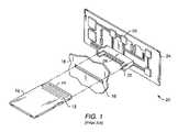
- FIG. 1illustrates a memory card 10 with edge connectors 12 .
- Edge connectors 12may be arranged on the backside surface of card 10 near a forward-leading edge 14 of card 10 .
- edge 14may be inserted through slot 16 extending through chassis 18 of an electronic system 20 .
- memory card 10may be inserted into receptor 22 , which may be electrically connected to, for example, another card 24 .
- card 24may also contain printed conductors and one or more integrated circuits 26 interconnected with each other on a surface of card 24 .
- card 10may include a specific purpose that may be universally applied to an electronic system, and may be obtainable from numerous vendors in the memory technology sector.
- card 10may be a memory card, and may utilize edge connectors 12 that may frictionally engage conductive elements 28 arranged within receptor 22 . In this manner, edge connectors 12 may be designed to releasably insert into receptor 22 .
- Card 10is illustrated in partial breakaway in FIG. 2 .
- Card 10may have one or more interconnected integrated circuits 30 which may also be connected to edge conductors 12 by trace conductors 32 .
- a memory cardpreferably uses a form of memory array.
- a popular memory arraymay involve an array of non-volatile storage elements.
- the non-volatile storage elementsmay be configured on a single monolithic silicon substrate to form a non-volatile memory integrated circuit 30 b .
- circuit 30 bmay be memory controller 30 a .
- card 10may also have mounted thereon discrete devices, such as decoupling or de-bounce capacitors 34 . Capacitors 34 may serve to minimize transient noise applied to trace conductors 32 .
- card 10may also include covering 36 .
- Covering 36may surround and protect the integrated circuits and capacitors mounted on card 10 .
- tab or switch 38may be formed as part of covering 36 , such that when moved, switch 38 may prevent a write operation to the memory integrated circuit. Switch 38 thereby suffices to “write protect” memory card 10 . If switch 38 is activated, any signal sent to edge conductors 12 to be written onto the storage elements of memory 30 b may be prevented from being stored. Activation may occur simply by moving switch 38 from one position to another along the sidewall surface of card 10 .
- the memory card 10 shown in the configuration of FIGS. 1 and 2gained popularity, for example, during the advent of flash memory. Flash memory may be easily erased and reprogrammed. Once reprogrammed, the data within the flash memory is said to be non-volatile and may remain until erased or again reprogrammed. Thus, card 10 may be erased and reprogrammed while in receptor 22 provided, of course, that switch 38 is not in the write protect position. Once programmed, any data stored within non-volatile memory 30 b of card 10 may remain, thereby allowing card 10 to be removed and reinserted at a later time whenever that data may be needed—similar to a floppy disk.
- memory cardshaving the aforesaid characteristics.
- Popular such memory cardsinclude: Sony's memory stick, compact flash, smart media, PC cards, flash path, multimedia cards and secure digital.
- All of the well-known memory cardstypically include both a memory controller and non-volatile memory mounted on the card itself, or the controller may form a part of the memory interface, all of which may be interconnected to the edge connectors.
- memory modulesthat include two or more die, such as a controller die and storage element, may also be called multi-chip modules (MCM).
- MCMmulti-chip modules
- the most common type of MCMmay be the side-by-side MCM, which may mount two integrated circuits (or two die) next to each other on the top surface of a package substrate. Interconnections between integrated circuits and conductive traces on the substrate may typically be achieved by wire bonding.
- the side-by-side MCMmay suffer from low package efficiency since the area of the package substrate generally increases with an increase in the number of integrated circuits mounted on the package substrate. Such an increase in package size may also increase the overall cost of the package.
- a multi-chip modulemay be created in which one or more die, for example, memory controller and memory array chip, may be stacked upon a package substrate to increase package efficiency.
- U.S. Pat. No. 6,252,305 to Lin et al.describes such a multi-chip module having a stacked chip arrangement.
- FIG. 3discloses a multi-chip module 31 comprising four chips 21 , 23 , 25 , 27 stacked upon each other and mounted to a substrate 29 .
- the MCMcomprises at least two semiconductor chips, such that each chip has a row of bonding pads formed on the active surface of the chip. However, the row of bonding pads may be disposed along only one side edge of the chip.
- the semiconductor chipsare mounted to a substrate in a stacking arrangement, such that an upper chip is bonded to the active surface of a lower chip in such a manner that no portion of the upper chip interferes (or covers) each bond pad of the lower chip.
- Such an arrangementmay permit wire bonding of the stacked chips to the underlying trace conductors 33 on the surface of package substrate 29 .
- mounting a multi-chip module in a substrate packagemay allow each chip in the stack to be wire bonded to the surface of the substrate along all four sides of the substrate.
- this bonding arrangementmay not be possible in other memory packaging configurations.
- the above bonding arrangementmay not be possible in memory card configurations, since memory card edge connectors (i.e. bonding pads) may be arranged along only one side of the card.
- the desired memory subsystemmay, however, avoid using a printed circuit board or card for electrical routing or as a backbone for mechanical stability.
- the desired memory subsystemmay be classified as a memory module made of less expensive materials and in less time than conventional memory cards.
- the desired memory subsystemmay avoid the most expensive component of a memory card by eliminating the cost and lead time needed to form package material about an integrated circuit, form printed conductors upon and within a card, and form the connection between leads of the integrated circuit and printed conductors upon (or within) the card.
- the desired memory subsystemmay integrate a memory and controller die in such a manner as to reduce the overall cost of the memory subsystem.
- the problems outlined abovemay be in large part solved by a multi-chip memory subsystem, having the dimensions and characteristics of a conventional memory card, without the time and expense in making such a card.
- the present memory cardprovides a multi-chip memory subsystem including two or more stacked integrated circuits encased by a molded resin having an outer surface on which the second end of each of the plurality of conductors terminates in a single row near an edge of the memory module.
- the stacked integrated circuitscomprise a memory chip and a controller.
- the memoryis a three-dimensional memory of the type described in the patents and applications listed in the cross-reference to related applications (paragraph one of this specification).
- the present memory cardprovides a multi-chip memory subsystem including two or more stacked integrated circuits bonded, according to one embodiment, to a lead frame structure.
- the multi-chip memory subsystempreferably includes a means to couple one or more stacked integrated circuits to edge connectors in a memory card package with the capability to utilize bonding pads on all four sides of the integrated circuits.
- the memory subsystemmay include a stacked pair of integrated circuits, which may include storage elements and a memory controller, and any capacitive elements needed to decouple signal lines on a single monolithic substrate.
- the first step in processing the memory modulemay entail bonding conductors to bonding pads of the stacked integrated circuit similar to techniques used to bond package leads to the integrated circuit when forming a packaged integrated circuit.
- the bonded conductorsmay be encased within an encapsulate to form a memory module with an outer dimension similar to those of conventional memory cards.
- the edge connectors attributable to a memory cardmay be arranged in similar fashion on the memory module, where the conductors may serve not only to connect to the integrated circuit bonding pads, but also a portion of each conductor may be presented as a substantially planar surface (i.e., pad) forming a corresponding edge connector.
- the memory modulemay include a plurality of conductors for coupling circuit elements within the memory module to circuit elements within an electronic device through corresponding conductors arranged in a receptor of the electronic device.
- the conductorsmay transmit electrical signals to and from the circuit elements via corresponding edge connectors.
- the conductorsmay also be formed having opposed first and second ends.
- the memory modulemay also include one or more integrated circuits. In this manner, the first end of the conductors may be coupled to bonding pads on one or more of the integrated circuits.
- the second end of the conductorsmay be shaped similar to edge connectors of a conventional memory card. Unlike conventional integrated circuit packaging, however, the present plurality of conductors may extend in only one direction from the integrated circuit.
- the memory modulemay further include a molded resin encasing the stacked integrated circuits, and having an outer surface on which the second end of the conductors may terminate in a single row near an edge of the memory module.
- the row of second endsmay extend flush with, or possibly extend slightly above or below, the outer surface of the molded memory module. As such, when inserted into a receptor of an electronic device, the second ends (i.e. edge connectors) may be retained only in surface contact with a corresponding planar conductive surface within the receptor.
- the second endsmay have a planar outer surface that releasibly connects with a corresponding planar outer surface of conductive elements within a receptor.
- the memory modulemay be inserted and removed (i.e., released) from the receptor.
- the row of second endsmay maintain electrical communication with the conductive elements of the receptor, in order to facilitate communication between the memory module and the electronic system.
- a memory modulemay be formed on a lead frame structure, such that the structure of the lead frame may be divided into first and second portions.
- the first portion of the lead framemay be adapted to receive a first integrated circuit.
- a second integrated circuitmay be stacked upon and coupled to the first integrated circuit.
- the first integrated circuitmay be an array of storage elements (i.e. memory) while the second integrated circuit may be a controller for the memory.
- a memory diemay be stacked upon a controller die, or any other combination of two or more integrated circuits may also be used. In this manner, stacking integrated circuits on a portion of a lead frame, instead of placing them side by side on a package substrate, may reduce the overall size, complexity, and/or cost of the memory module.
- the second portion of the lead framemay include a plurality of conductors having opposed first and second ends.
- a first set of the plurality of conductorsmay be laterally spaced from the first portion of the lead frame.
- a first set of wiresmay extend between bonding pads of the stacked integrated circuits and the first end of the first set of conductors (i.e. conductive “bonding fingers” of the first set of conductors).
- the second end of each of the plurality of conductorsmay be adapted for frictional engagement with conductive elements arranged within a receptor of an electronic device. During times when the edge of the memory module may be slid into the receptor, the second end of the first set of conductors (i.e. edge connectors) may maintain an electrical connection with the conductive elements, or corresponding edge connectors, within the receptor.
- a second set of wireswhich transmit power and ground signals, may extend between the stacked integrated circuits and the first portion of the lead frame.
- the first portion of the lead framemay be laterally coupled to a second set of the plurality of conductors.
- the first portionmay be adapted to couple at least one of the stacked integrated circuits to power and ground connections on the second set of conductors.
- the first portionmay include power and ground planar elements.
- the power elementmay extend as a conductive ring coplanar with and laterally spaced from the ground element, such that the ground element may be the paddle portion of the lead frame.
- a first one of the second set of conductorsmay be adapted to connect the conductive ring to a power signal (or any other signal).
- a second one of the second set of conductorsmay be adapted to connect the ground element to a ground signal (or any other signal).
- the ground elementmay be adapted to transmit a power signal and the conductive ring may be adapted to transmit a ground signal.
- the first portionmay be adapted to couple any two bonding pads of the plurality of conductors to bonding pads on any side of an integrated circuit.
- a lead framemay be divided into first and second portions.
- the first portion of the lead framemay be configured to receive a first integrated circuit.
- a second integrated circuitmay also be stacked upon and coupled to the first integrated circuit.
- the first integrated circuitmay be a memory while the second integrated circuit may be a controller.
- a memory diemay be stacked upon and coupled to a controller die, or any other combination of two or more integrated circuits may also be used to create a stacked configuration.
- the first portion of the lead framemay be further separated into first and second coplanar elements.
- the second portion of the lead framemay include a plurality of conductors, where a first conductor from among the first set of conductors may extend toward and connect with the first coplanar element of the first portion. Likewise, a second conductor from among the plurality of conductors may extend toward and connect with the second coplanar element of the first portion. In this manner, the first conductor may transmit a power signal to the first coplanar element, while the second conductor may transmit a ground signal to the second coplanar element. Alternatively, the first conductor may transmit a ground signal to the first coplanar element, while the second conductor may transmit a power signal to the second coplanar element. In any case, all other of the first set of conductors, except for the first one and second one, may be spaced from the first portion.
- a lower surface of the first integrated circuitmay be bonded to the first portion (i.e. paddle) of the lead frame in such a manner as to bond with at least a portion of each of the first and second coplanar elements (i.e. bifurcated paddle) of the lead frame.
- the second integrated circuitmay be stacked upon and bonded to the upper surface of the first integrated circuit.
- the first portion of the lead framemay be a conductive plate, such that the first and second coplanar elements of the first portion may be adapted to transmit power and ground signals (or two dissimilar signals).
- the bifurcated paddle, or first portionmay also be adapted to extend beyond the dimensions of the stacked integrated circuits.
- the bifurcated paddle of the lead framemay be adapted to couple two dissimilar signals from the first set of conductors to bonding pads on one or more sides of the integrated circuits.
- the first set of the plurality of conductorsmay extend into an opening created within the lead frame.
- the conductorstherefore, may form a part of the lead frame used in wire bonding processes.
- the first end of one or more of the plurality of conductorsmay be secured directly to a bonding pad of an integrated circuit using, for example, a wire coupled between the lead frame post, or conductor, and a bonding pad on an integrated circuit.
- integrated circuitsmay be placed side-by-side on a laminate-based Ball Grid Array (BGA) package, allowing routing between the two die via metal trace interconnects on the laminate material.
- BGABall Grid Array
- the first end of one or more of the first set of conductorsmay be wire bonded to a bonding pad on an integrated circuit mounted on the BGA package.
- placing die side-by-side, rather than in a stacked configurationmay not solve the real estate reduction objective.
- laminate material chip carriersmay be more expensive than metal lead frame based chip carriers by an order of magnitude.
- a lead frame structuremay be used, such that the lead frame post coupled to the bonding pad by a wire bond may be specially designed.
- the post (or conductor)may extend, for example, in two planes whereby a first plane may be above or coplanar with a first portion (or paddle) on which the integrated circuit may be secured.
- a second part of the conductormay be configured parallel to and below the first plane, such that the post (or conductor) may extend along the first plane downward at an angle to the second plane.
- the downward anglemay be less than ninety degrees, and preferably less than 60 degrees from a horizontal plane.
- the second part, as well as the angled joinder of the first and second partsmay be encompassed entirely within a resin encapsulate.
- the part of the conductor that occupies the second planemay form the edge connector and, therefore, may be brought flush with the outer surface of the memory module.
- the part that extends along the first planemay be adapted to receive a wire bond.
- the conductor or lead framemay suffice not only to convey signals to and from an integrated circuit, but may also be shaped to extend both within the memory module encapsulate material and outside the encapsulate material.
- the memory modulemay be formed using a simple pair of mold housings, such that the integrated circuit purposely avoids having to rest upon any mechanical support other than, for example, a first portion (or “paddle”) of a lead frame.
- the pair of mold housingsmay thereby form a cavity that surrounds the lead frame-bonded integrated circuit.
- the pair of mold housingsmay include an opening, which may allow liquid resin to be inserted into the cavity.
- the inner walls of the pair of mold housings that form the cavitymay be dimensioned according to the standards of a memory card device with associated width, height, and length configuration of a conventional memory card. Thus, the mold cavity may be much larger than the silicon substrate of an un-packaged integrated circuit.
- the mold cavitymay form the memory module by filling the cavity with a flowable encapsulate to surround the lead frame and attached integrated circuits. In this manner, no intervening card or substrate may be necessary to support the integrated circuits, as opposed to conventional designs in which packaged integrated circuits may be mounted on a card, or flip-chip secured to a substrate that may be mounted to a card.
- FIG. 1is a perspective view of a conventional memory card having edge connectors adapted for insertion through a slot of an electronic system, according to one memory card attachment methodology;
- FIG. 2is a perspective view of the memory card in FIG. 1 with packaged integrated circuits mounted upon a rigid printed circuit board and encased in a covering;
- FIG. 3discloses a multi-chip module mounted on a substrate base bearing trace conductors
- FIG. 4Ais an illustration of a wire-bonded, stacked pair of integrated circuits
- FIG. 4Bis a detailed block diagram of one embodiment of an integrated circuit
- FIG. 5is a cross-sectional view of one embodiment of a three-dimensional memory array
- FIG. 6is a perspective view of stacked integrated circuits, including a three-dimensional memory array, incorporated onto a substrate package;
- FIG. 7is a perspective view of stacked integrated circuits incorporated onto a lead frame package
- FIG. 8is a cross sectional view along plane 8 of FIG. 7 , with a first integrated circuit coupled to a conductive ring and to the paddle portion of the lead frame, the second integrated circuit coupled to the edge connectors of the lead frame, and a pair of mold housings suspended around the stacked integrated circuits such that resin may be poured into the space between the mold housings and the integrated circuits;
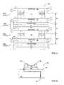
- FIG. 9is a perspective view of stacked integrated circuits incorporated onto a lead frame package having a bifurcated paddle, according to a second embodiment
- FIG. 10Ais a cross sectional view along plane 10 A of FIG. 9 , depicting the stacked integrated circuits bonded to the first element of the bifurcated paddle, and a pair of mold housings suspended around the stacked integrated circuits such that resin may be poured into the space between the mold housings and the integrated circuits;
- FIG. 10Bis a cross sectional view along plane 10 B of FIG. 9 , depicting the stacked integrated circuits bonded to the second element of the bifurcated paddle, and a pair of mold housings suspended around the stacked integrated circuits such that resin may be poured into the space between the mold housings and the integrated circuits;
- FIG. 11is a cross-sectional view along plane 8 of FIG. 7 after the mold housings and a portion of the hardened resin has been removed to expose edge connectors arranged in a row along the backside of the memory module;
- FIG. 12is a cross-sectional view of an alternative configuration in which the edge connectors may be bent downward to form a conductive surface that is flush with the outer surface of the memory module;
- FIG. 13is a cross-sectional view of another alternative configuration in which the lead frame paddle may lie along the same plane as the exposed edge connectors in order to provide a thermal sink;
- FIG. 14is cross-sectional view along a lateral plane of the first embodiment illustrating how power and ground signals may be transmitted to the stacked integrated circuits on all four sides of the integrated circuits.
- FIG. 4Aillustrates the interconnection between two or more integrated circuits using a wire bonding process.
- the lower or first integrated circuit 40 bmay include a storage element attributable to semiconductor memory devices.
- first integrated circuit 40 bmay also include a multi-level array of storage cells as described in the commonly assigned U.S. patent application Ser. No. 09/814,727, or any of the patents or applications set forth in the cross-reference section (paragraph one) of this application.
- the upper or second integrated circuit 40 amay include similar circuitry, or may include different technology all together.
- the second integrated circuit 40 amay include a controller for the storage element.
- the controller for the semiconductor memorymay be bonded to the top surface of the memory using a die attach adhesive.
- the die attach adhesivemay be tape or epoxy based.
- a wire bonding machinewhich may operate much like a sewing machine, may attach individual wires between bonding pads 42 on the active surface of each die, in such a manner as to achieve the required system functionality and communication between the memory, controller, and the outside world.
- bonding pads 42 a of integrated circuit 40 amay be directly attached to bonding pads 42 b of integrated circuit 40 b with such a wire bonding process.
- the wires used in the wire bonding processmay typically be aluminum, since aluminum is a good conductor and does not sag like softer materials (for example, gold).
- FIG. 4Bindicates the various components that may be found on a single integrated circuit, in one example.
- integrated circuit 41may be a single die within multiple dice arranged across a semiconductor wafer.
- Integrated circuit 41may represent the culmination of multiple processes applied to a single crystalline silicon base material. Such processes may include implantation, deposition, etching, cleaning, and polishing steps, among others.
- Integrated circuit 41may not be placed in a package after it is scribe-removed from the wafer.
- integrated circuit 41may be highly integrated, and may include the various circuits needed to store and recall data. Those circuits may also include an array of memory cells that, according to one example, may be based on non-volatile memory cells 44 .
- the mechanism responsible for directing data to and from memory cells 44may involve memory controller 46 .
- Memory controller 46may be arranged on-chip, as in the example depicted in FIG. 4B . Alternatively, memory controller 46 may be arranged off-chip. As shown in FIG. 4A , a memory controller may also be coupled to memory as a separate die (i.e. integrated circuit 40 a and 40 b , respectively).
- decoupling capacitors 48may be used to maintain a more pristine characteristic of the data sent to and from memory cells 44 .
- decoupling capacitors 48may be incorporated into an integrated circuit along with memory cells 44 and memory controller 46 .
- decoupling capacitors 48may be arranged on a separate controller die, as described in reference to FIG. 4A .
- conductors 49may transmit data and control signals, and may extend to bonding pads on an integrated circuit. Thus, in the illustrated example, conductors 49 may terminate at bonding pads 43 of integrated circuit 41 .
- first integrated circuit 40 bmay include a multi-level array of storage cells (i.e. three-dimensional memory array) as described in any of the patents or applications set forth in the cross-reference section (paragraph one) of this application.
- a three-dimensional memory arraymay be fabricated on several levels and may have eight levels of storage, in one example.
- each level of storagemay include a plurality of parallel rail-stacks aligned in a first direction and another plurality of rail-stacks or conductors aligned in a second direction.
- Such a second directionmay be substantially perpendicular to the first direction, thereby forming right angles at the intersections between rail-stacks.
- a bitmay be stored at each of the intersections of the perpendicular rail-stacks, such that memory cells may be defined by the rail-stacks and intermediate layers.
- FIG. 5illustrates one embodiment of a three-dimensional memory array that may be included as first integrated circuit 40 b in the memory module of the present invention.
- FIG. 5only three complete levels 50 , 51 , and 52 of the memory array are depicted for purposes of simplicity. However, the memory array may include additional levels above and/or below the levels shown.
- the memory arraymay also be fabricated on a substrate, which may include a plurality of conductors. Also, vias may connect conductors within the rail-stacks to trace conductors within the substrate to read (or write) data from (or to) the memory array.
- each of the memory array rail-stacksmay be a full or half set, such that half rail-stacks may be approximately half the thickness of the full set of rail-stacks used in subsequent levels.
- insulating antifuse layersmay be used to separate adjacent rail-stacks.
- rail-stack 3may be a full rail-stack including a lightly doped n ⁇ layer, a heavily doped n+ layer, a conductor layer, and a second n+ layer.
- the n+ layersmay be formed above and below the conductor layer to prevent unintended Schottky diode formation.
- Antifuse layer 53may be formed from a dielectric material, such as silicon dioxide, in one example, and may separate rail-stack 3 from neighboring rail-stack 4 .
- Rail-stack 4may be a half rail-stack formed above antifuse layer 53 , and may include a lightly doped p ⁇ layer, a first p+ layer, a conductor layer, and a second p+ layer. After deposition, the layers of rail-stack 4 may be masked and etched to form the structures of half rail-stack 4 . Lines 57 in FIG. 5 may indicate that antifuse layer 53 (and similar layers) may not be etched with the rail-stack and may extend over the entire array, thus reducing sidewall leakage into rail-stacks below.
- the etching processmay also form voids between portions of half rail-stacks, such as void 58 within rail-stack 4 , which may be filled with a dielectric material.
- the fillmay be planarized along with a portion of the second p+ layer to control the thickness and contour of the fill.
- Antifuse layer 54may be deposited on top of rail-stack 4 .
- the processmay be repeated by forming rail-stacks 5 and 6 similar to the formation of rail-stacks 3 and 4 , respectively, or until the 3-D memory array may be completed.
- a relatively high voltage(e.g. 5-20V) may be applied between the conductors of neighboring rail-stacks.
- a relatively high voltagemay cause a breach in the antifuse layer, thereby creating a diode at the intersection between rail-stacks.
- each conductormay constitute a bit line for the “cells” above and below it.
- the absence of such a voltagemay permit the antifuse layer to retain its insulating properties. Therefore, diodes may be selectively formed to program the memory array by applying a voltage to select pairs of conductors.
- datamay be read from the 3-D memory array by applying a voltage that is substantially lower than the voltage used to write data into the array.
- FIG. 6illustrates a first embodiment of the multi-chip module of the present invention in which stacked integrated circuits 40 may be incorporated onto substrate 62 .
- Stacked integrated circuits 40may include controller 40 a and storage element 40 b , such that controller 40 a may be stacked upon and bonded to storage element 40 b .
- controller 40 amay also be electrically coupled to storage element 40 b through a wire bonding process (i.e. wire bond 68 ).
- controller 40 amay be coupled to storage element 40 b by another bonding process, such as tape automated bonding (TAB) or flip-chip attachment.
- TABtape automated bonding
- storage element 40 bmay be a three-dimensional memory array, as described above.
- Memory module 60 of FIG. 6may also include a first set of wires 69 extending between controller 40 a and trace conductors 64 .
- Trace conductors 64may be arranged on the surface of substrate 62 and/or embedded within the thickness of substrate 62 .
- Trace conductors 64may, therefore, include one or more layers of trace conductors, each of which may be separated by a dielectric layer.
- Trace conductors 64may extend along one or more of layers of the substrate, and may connect leads of at least one integrated circuit to a plurality of conductors 66 through plated-through holes, or vias.
- the memory modulemay further include a molded resin encasing stacked integrated circuits 40 and substrate 62 , such that the memory module may include an outer surface having dimensions substantially equal to the dimensions of a conventional memory card.
- the plurality of conductors 66may also be shaped similar to edge connectors of a conventional memory card, and may be arranged in a single row near a forward leading edge of memory module 60 . Additionally, the row of conductors 66 may extend flush with, or possibly extend slightly above or below, the outer surface of the molded memory module. In this manner, memory module 60 may be inserted into a receptor of an electronic device, such that the row of conductors (i.e. edge connectors) may be retained in surface contact with a corresponding planar conductive surface within the receptor.
- FIG. 7illustrates a second embodiment of the multi-chip module of the present invention in which stacked integrated circuits 40 may be incorporated onto lead frame 70 .
- first integrated circuit 40 bmay be a three-dimensional memory array, as described above.
- the scope of the present inventionmay include any storage element, or any other integrated circuit.
- Lead frame 70may contain a first portion 72 (i.e. paddle) that may be configured below stacked integrated circuits 40 .
- Integrated circuits 40may be bonded to the first portion of lead frame using, for example, a die attach adhesive.
- the die attach adhesivemay be tape or epoxy based.
- lead frame 70may serve to support the molded memory module, and thus, may be fabricated from a strip of sheet metal by stamping or chemical milling.
- Lead frame 70may also provide a holding fixture during the assembly process in which bonding pads 42 of integrated circuits 40 may be connected to the lead frame. After molding, lead frame 70 may become an integral part of the memory module.
- the lead framemay be fabricated from numerous materials, including nickel-iron or copper alloy.
- the lead framemay also be layered as a composite strip, such that a copper alloy may be placed upon a stainless steel structure.
- the lead framemay be conductive.
- first portion 72 of lead frame 70Extending outward from first portion 72 of lead frame 70 may be support members 74 . Support members 74 may thereby secure the position of first portion 72 relative to a frame 76 encircling first portion 72 . Extending inward from one side of frame 76 may be a plurality of conductors 78 . Each conductor 78 may include a first portion 78 a and a second portion 78 b . First portion 78 a may be relatively narrow in upper surface area, while second portion 78 b may be much wider. Portions 78 a and 78 b may be formed from a single piece of conductive material and may extend as an integral piece with items 72 , 74 and 76 . Thus, first portion 72 , support members 74 , frame 76 , and conductors 78 may be formed from the same sheet, such that each item may be stamped from that sheet.
- FIG. 8illustrates a cross sectional view along plane 8 of FIG. 7 after bonding stacked integrated circuits 40 to first portion 72 of lead frame 70 .
- a first integrated circuit 40 bsuch as a semiconductor memory
- Die attach adhesive 86may include silicon/gold eutectic bonding or may use a polymer adhesive base.
- die attach adhesive 86may include any structure that securely fastens stacked integrated circuits 40 to first portion 72 .
- die attach adhesive 86is not electrically conductive, however, adhesive 86 may include thermal conducting properties.
- a second integrated circuit 40 asuch as a controller, may then be stacked upon and bonded to an opposing surface of the first integrated circuit using die attach adhesive 86 .
- a memory diemay be stacked upon a controller die, or any other combination of two or more integrated circuits may be used to form a stack of integrated circuits.
- the individual diemay be electrically coupled to one another through a wire bonding process, which may attach individual wires between the bonding pads of each die, such that communication between the die may be achieved.
- bonding pads 42 b of integrated circuit 40 bmay be wire bonded to bonding pads 42 a of integrated circuit 40 a , such that integrated circuits 40 a and 40 b may be electrically and mechanically coupled to one another.
- integrated circuit 40 amay also be coupled to a first set of the plurality of conductors 78 .
- a first set of wiresmay extend between bonding pads 42 a of integrated circuit 40 a and bonding pads arranged on first portion 78 a of conductors 78 .
- Conductors 78may be adapted for frictional engagement with, and electrical connection to, conductive elements arranged within a receptor of an electronic device. In this manner, integrated circuit 40 a may be coupled to internal circuitry of the electronic device.
- a second set of wiresmay extend between first integrated circuit 40 b and first portion 72 , such that the second set of wires may only transmit power and ground signals to integrated circuit 40 b .
- the first portion of the lead framemay be laterally coupled to a second set of the plurality of conductors 78 .
- the first portionmay be adapted to couple at least one of the stacked integrated circuits to dedicated power and ground conductors (i.e. second set of the plurality of conductors) from among conductors 78 .
- first portion 72may include power and ground planar elements.
- the power elementmay extend as conductive ring 72 b coplanar with and laterally spaced from the ground element (such that the ground element 72 a may be the paddle portion of the lead frame structure).
- Conductive ring 72 bmay be separated from ground element 72 a by an air gap on all four sides of ground element 72 a . In this manner, conductive ring 72 b may be electrically isolated from ground element 72 a in subsequent processing steps (i.e. when encapsulated with mold compound).
- first one of the second set of conductorsmay be adapted to connect conductive ring 72 b to a power signal (or any other signal).
- second one of the second set of conductorsmay be adapted to connect ground element 72 a to a ground signal (or any other signal).
- ground element 72 amay be adapted to transmit a power signal
- conductive ring 72 bmay be adapted to transmit a ground signal.
- first portion 72may extend flush with or beyond the outer dimension of the stacked integrated circuits. In this manner, first portion 72 may be adapted to couple power and ground signals to bonding pads on any side of an integrated circuit.
- first portion 72may be adapted to couple any two bonding pads of conductors 78 to bonding pads on any side of an integrated circuit. Therefore, the above embodiments of the present invention may provide a means to couple one or more stacked integrated circuits to lead frame conductors with the capability to utilize bonding pads on all four sides of an integrated circuit.
- FIG. 8also indicates that once conductors 78 of lead frame 70 are secured and electrically connected to corresponding bonding pads on integrated circuit 40 a , conductors 78 may be retained between a pair of mold housings 82 , and liquid resin 88 may be injected into the air-filled space surrounding integrated circuit 40 a . Contrary to ceramic packaging techniques which may leave an air-filled space between the integrated circuit and the package inner surface, the present technique purposely fills that space with an encapsulate that also suffices as the memory module encasement. Thus, after removing the pair of mold housings 82 , the resin may extend outward from the integrated circuit to form an outer surface of memory module 80 .
- the resinmay be any inert component that is not electrically conductive, yet may include some thermal conductive properties.
- the resinmay consist of silicones, phenolics, and bisphenols (epoxy).
- the resinmay also contain various curing agents, hardeners, accelerators, inert fillers, coupling agents, flame-retardants, stress-relief additives, coloring agents, and mold-release agents.
- resin 88may be injected in liquid form into the cavity between the inward-facing surfaces of mold housings 82 . After the liquid resin has had sufficient time to cure, the resin may harden to the form and dimensions of a conventional memory card.
- FIG. 11illustrates memory module 80 after removal of the pair of mold housings 82 .
- Memory module 80may be formed of hardened resin material 110 , which may encompass integrated circuits 40 and conductors 78 .
- the hardened resinmay serve to protect integrated circuits 40 from ingress of moisture, and may provide a mechanical support for the integrated circuits.
- a covering 120may be placed around the hardened resin.
- covering 120may be made of plastic that is heat-shrunk to fit the outer dimensions of the molded resin, or may be glued or welded at the joint between a two-part assembly of the covering.
- Memory card 80may, therefore, be formed either with or without covering 120 .
- a mechanical switch or tabmay be formed within the covering, similar to item 38 shown in FIG. 2 .
- mechanical tab 38may prevent writing data to integrated-circuits 40 when mechanical tab 38 is activated.
- the switchmay be snap assembled to slots formed in resin 110 .
- the hardened resinmay be partially removed to expose the outer planar surfaces of conductors 78 . Removal may take place either by back-lapping or etching of the molded resin to expose conductors 78 as the edge connectors of the memory module. Beneficially, the removal process may be employed on the backside surface of the memory module near the forward-leading edge, so that the forward-leading edge may be inserted into a receptor bearing corresponding conductive elements. Alternatively, the molding process may leave the pad areas free of resin, for example, by forming the mold cavity so that a recess may be formed to expose conductors 78 , thereby forming edge connectors.
- the hardened resin 110may or may not be encircled by a covering and, as shown in FIG. 11 , no covering need be present.
- FIG. 12illustrates the use of covering 120 and, more importantly, depicts a bend placed in conductors 78 of the lead frame.
- Conductors 78may thereby be shown with a first part 122 .
- First part 122may be substantially coplanar with first portion 72 of the lead frame, and may be adapted to receive a wire bond of wire 126 .
- Conductors 78therefore, may extend along a first plane substantially coplanar to first portion 72 , and may further extend downward at an angle to a second plane at which second part 124 may reside.
- Second part 124may have an outer surface that may extend flush with the outer surface of hardened resin 110 . As such, second part 124 may be exposed at the forward-leading edge of memory module 80 .
- second part 124may consist of a widened surface (see FIG. 7 ) that may be adapted to frictionally engage conductive elements within a receptor of an electronic device, in one example. In this manner, bending one or more conductors within the row of conductors 78 may expose the second part 124 of each conductor. Thus, bending the conductors in the above manner may substantially form a row of edge connectors at the forward-leading edge of memory module 80 .
- the edge connectorsmay be slightly offset from each other along a single axis.
- edge connectors within a rowmay be offset from the axis, the edge connectors nonetheless may maintain somewhat of an alignment along a line relative to one another.
- First portion 72 , conductive ring 79 , and integrated circuits 40may remain suspended entirely within hardened resin 110 .
- FIG. 13illustrates an alternative arrangement of the second embodiment, in which first part 122 of conductors 78 may be arranged in a plane above first portion 72 .
- first part 122 of conductors 78may be arranged in a plane above first portion 72 .
- the first part 122 of FIG. 13may be arranged above the plane formed by first portion 72 , such that second part 124 may be coplanar with first portion 72 .
- FIG. 13therefore, illustrates elevating conductors 78 above first portion 72 to not only expose second part 124 as an edge connector, but also to expose the backside surface of first portion 72 .
- first portion 72may be conductive elements, and that die adhesive 86 may be thermally conductive.
- thermally conductive elements 86 and 72may operate as a heat sink to remove heat from integrated circuit 40 b .
- conductors 78may extend in a single plane, as depicted in FIG. 11 , such that conductors 78 may be exposed as edge connectors.
- FIG. 14is top plane view along a lateral plane of the memory card as described in the second embodiment of the present invention.
- Memory card 80may include integrated circuit 40 a stacked upon and bonded to integrated circuit 40 b .
- Each of the integrated circuits 40may have an upper active surface that may include bonding pads 42 arranged along all four sides of the active surface. In this manner, bonding pads 42 a of integrated circuit 40 a may be coupled to bonding pads 42 b of integrated circuit 40 b , such that bonding pads may be utilized on all four sides of the integrated circuits.
- memory card 80may include a plurality of conductors 78 that may be arranged on a forward-leading edge of the memory module.
- Memory card 80may also include a molded resin extending completely around the stacked integrated circuits to form an outer dimension of the memory module. Subsequently, conductors 78 may be exposed in a manner as described above, thereby forming a row of edge connectors on the forward-leading edge of the memory card.
- Memory card 80may further include a lead frame, in which first portion 72 of the lead frame may extend beyond the outer dimensions of integrated circuits 40 . A first set of the plurality of conductors may be spaced laterally from first portion 72 , while a second set of the plurality of conductors may be laterally coupled to first portion 72 .
- first portion 72may be adapted to electrically couple integrated circuits 40 to the second set of edge conductors 78 .
- First portion 72may also be mechanically coupled to the lead frame with support members 140 and 142 .
- Support members 140 and 142are arranged on a lateral plane separate from conductors 78 , such that support members 140 and 142 may be dielectrically spaced and electrically isolated from conductors 78 .
- first portion 72may include power and ground planar elements.
- the power elementmay extend as conductive ring 72 b coplanar with and laterally spaced from ground element 72 a .
- conductive ring 72 bmay be separated from ground element 72 a by an air gap on all four sides of ground element 72 a .
- conductive ring 72 bmay be electrically isolated from ground element 72 a by filling the air gap with mold compound during the encapsulation of the memory module.
- ground element 72 a and conductive ring 72 bmay be adapted to couple integrated circuits 40 to at least a portion of conductors 78 , such that bonding pads 42 may be utilized on all four sides of integrated circuits 40 .
- ground element 72 amay be adapted to couple a ground signal from a first conductor of the second set of conductors 78 to a bonding pad on any of the four sides of an integrated circuit.
- conductive ring 72 bmay be adapted to couple a power signal from a second conductor of the second set of conductors 78 to a bonding pad on any of the four sides of an integrated circuit.
- ground element 72 amay be adapted to transmit a power signal and conductive ring 72 b may be adapted to transmit a ground signal.
- first portion 72may be adapted to couple any two conductors of the plurality of conductors 78 to bonding pads on any side of an integrated circuit.
- FIG. 9illustrates yet another embodiment of the multi-chip module of the present invention in which stacked integrated circuits 40 may be incorporated onto lead frame 90 .
- Lead frame 90may be configured similarly to lead frame 70 of FIG. 7 , such that lead frame 90 may include first portion 92 , support members 94 , frame 96 , and conductors 98 .
- Conductors 98may also include first portion 98 a and second portion 98 b , similar in configuration to conductors 78 of lead frame 70 (shown in FIG. 7 ).
- first portion 92 , support members 94 , frame 96 , and conductors 98may be formed from the same sheet, such that each item may be stamped from that sheet.
- first portion 92 of lead frame 90may be configured to receive a first integrated circuit 40 b .
- a second integrated circuit 40 amay also be stacked upon and coupled to the first integrated circuit.
- first integrated circuit 40 bmay be a three-dimensional memory array, as described above.
- the scope of the present inventionmay include any other storage element or integrated circuit.
- first integrated circuit 40 bmay be a semiconductor memory while second integrated circuit 40 a may be a controller.
- memorymay be stacked upon and coupled to a controller, or any other combination of two or more integrated circuits may also be used to create such a stacked configuration.
- first portion 92 of lead frame 90may be further separated into first and second coplanar elements 92 a and 92 b , respectively.
- the second portion of lead frame 90may include a plurality of conductors 98 , such that a first conductor from among the plurality of conductors may extend toward and connect with first coplanar element 92 a of the first portion. Likewise, a second conductor from among the plurality of conductors 98 may extend toward and connect with second coplanar element 92 b of the first portion. In this manner, the first conductor may transmit a power signal to first coplanar element 92 a , while the second conductor may transmit a ground signal to second coplanar element 92 b . In an alternative example, the first conductor may transmit a ground signal to the first coplanar element, while the second conductor may transmit a power signal to the second coplanar element.
- the first and second conductorsmay transmit any two signals that may be necessary to the functionality of integrated circuits 40 .
- all other of the first set of conductors 98except for the first one and second one, may be spaced from the first portion.
- FIGS. 10A and 10Billustrate cross sectional views along planes 10 A and 10 B of FIG. 9 after bonding stacked integrated circuits 40 to first portion 92 of lead frame 90 .
- Plane 10 Ais a cross sectional view of FIG. 9 including first coplanar element 92 a , illustrating the coupling between integrated circuit 40 b and first coplanar element 92 a .
- plane 10 Bis a cross sectional view of FIG. 9 including second coplanar element 92 b , illustrating the coupling between integrated circuit 40 b and second coplanar element 92 b.
- a first integrated circuit 40 bsuch as a memory die, may be bonded to first portion 92 in such a manner as to bond integrated circuit 40 b with at least a portion of each of the first and second coplanar elements (i.e. bifurcated paddle) of the lead frame.
- Die attach adhesive 106may be used to bond integrated circuit 40 b to first portion 92 .
- Die attach adhesive 106may include silicon/gold eutectic bonding or may use a polymer adhesive base.
- die attach adhesive 106may include any structure that securely fastens integrated circuit 40 b to first portion 92 .
- die attach adhesive 106may not be electrically conductive, die attach adhesive 106 may include thermal conducting properties.
- a second integrated circuit 40 amay be stacked upon and bonded to an opposing surface of the first integrated circuit using die attach adhesive 106 .
- the individual diemay be electrically coupled to one another through a wire bonding process, which may attach individual wires between the bonding pads of each die, such that communication between the die may be achieved.
- bonding pads 42 b of integrated circuit 40 bmay be wire bonded to bonding pads 42 a of integrated circuit 40 a , such that integrated circuits 40 a and 40 b may be electrically and mechanically coupled to one another.
- integrated circuit 40 amay also be coupled to the plurality of conductors 98 .
- a first set of wiresmay extend between bonding pads 42 a of integrated circuit 40 a and bonding pads arranged on a first portion 98 a of conductors 98 .
- integrated circuit 40 amay be coupled to internal circuitry of an electronic device via conductors 98 , such that conductors 98 may be adapted for frictional engagement with, and electrical connection to, conductive elements arranged within a receptor of the electronic device.
- first portion 92may be a bifurcated conductive plate, such that the first and second coplanar elements 92 a , 92 b of the first portion may be adapted to transmit power and ground signals.
- the bifurcated paddle, or first portion 92may also be adapted to extend beyond the dimensions of the stacked integrated circuits.
- first coplanar element 92 amay extend beyond the lateral extents of a first portion of the stacked integrated circuits.
- second coplanar element 92 bmay extend beyond the lateral extents of a second portion of the stacked integrated circuits.
- first coplanar element 92 amay be connected by a first conductor of conductors 78 to a ground signal (or power signal), while second coplanar element 92 b may be connected by a second conductor of conductors 78 to a power signal (or ground signal).
- the memory module of the present embodimentmay be completed in the manner as described in FIGS. 8 and 11 - 13 .
- conductors 98may be retained between a pair of mold housings 102 , and liquid resin 108 may be injected into the air-filled space surrounding integrated circuits 40 .
- first coplanar element 92 amay be laterally spaced from second coplanar element 92 b
- the liquid resin injected into the mold cavitymay fill the common space to electrically isolate the two coplanar elements.
- Liquid resin 108may harden, and subsequently, the pair of mold housings 102 may be removed.
- the resinmay extend outward from the stacked integrated circuits to form an outer surface of memory module 100 , such that memory module 100 may exhibit the form and dimensions of a conventional memory card.
- the hardened resinmay also serve to protect integrated circuits 40 from ingress of moisture, and may further provide a mechanical support for the integrated circuits.
- the molded resinmay be partially removed by a back-lapping or etching process to expose conductors 98 as the edge connectors of memory module 100 .
- a bendmay be employed within conductors 98 , such that back-lapping or etching of the molded resin may not be necessary to expose the edges of conductors 98 .
- conductors 98may substantially form a row of edge connectors at the forward-leading edge of memory module 100 .
- conductors 98may be elevated above first portion 92 to expose a second part of conductor 98 as an edge connector, as well as to expose the backside surface of first portion 92 .
- any heat build-up within integrated circuit 40 bmay be transferred downward to the thermally conductive adhesive 106 and first portion 92 .
- the thermally conductive first portion 92may operate as a heat sink to remove heat from integrated circuit 40 b .
- conductors 98may extend along a common plane with first portion 92 , such that the backside surfaces of conductors 98 and first portion 92 may be exposed.
- a memory modulethat may be mounted on a substrate or lead frame of a memory card package and may include one or more stacked integrated circuits.
- the memory module of the present inventionmay also provide a means to couple one or more of the stacked integrated circuits to substrate or lead frame conductors with the capability to utilize bonding pads on all four sides of the integrated circuits.
- the improved memory modulemay have further modifications and alternative forms to include various aspects of the present invention, as will be apparent to those skilled in art after having reviewed this description. Thus, it is intended that the following claims be interpreted to embrace all such modifications and changes and, accordingly, the specification and drawings are to be regarded in an illustrative rather than restrictive sense.
Landscapes
- Engineering & Computer Science (AREA)
- Microelectronics & Electronic Packaging (AREA)
- Computer Hardware Design (AREA)
- Physics & Mathematics (AREA)
- General Physics & Mathematics (AREA)
- Power Engineering (AREA)
- Condensed Matter Physics & Semiconductors (AREA)
- Theoretical Computer Science (AREA)
- Geometry (AREA)
- Semiconductor Memories (AREA)
Abstract
Description
- U.S. Pat. Nos. 6,034,882 and 6,185,122, both titled “Vertically Stacked Field Programmable Nonvolatile Memory and Method of Fabrication”, by inventor Mark G. Johnson et al.;
- U.S. patent application Ser. No. 09/814,727 and Ser. No. 09/560,626, both titled “Three Dimensional Memory Array and Method of Fabrication”, by Johan Knall et al, filed Apr. 21, 2001 and Apr. 28, 2000, respectively;
- U.S. patent application Ser. No. 09/928,536 titled “Vertically Stacked, Field Programmable, Nonvolatile-Memory and Method of Fabrication” by Mark G. Johnson, filed Aug. 13, 2001;
- U.S. patent application Ser. No. 10/010,643, titled “Insulator Programmed Mask ROM Memory Cells for a 3-Dimensional Memory Array”, by Mark G. Johnson, filed Nov. 5, 2001;
Claims (11)
Priority Applications (1)
| Application Number | Priority Date | Filing Date | Title |
|---|---|---|---|
| US11/326,074US7432599B2 (en) | 2002-02-19 | 2006-01-05 | Memory module having interconnected and stacked integrated circuits |
Applications Claiming Priority (3)
| Application Number | Priority Date | Filing Date | Title |
|---|---|---|---|
| US10/080,036US6731011B2 (en) | 2002-02-19 | 2002-02-19 | Memory module having interconnected and stacked integrated circuits |
| US10/793,407US7005730B2 (en) | 2002-02-19 | 2004-03-04 | Memory module having interconnected and stacked integrated circuits |
| US11/326,074US7432599B2 (en) | 2002-02-19 | 2006-01-05 | Memory module having interconnected and stacked integrated circuits |
Related Parent Applications (1)
| Application Number | Title | Priority Date | Filing Date |
|---|---|---|---|
| US10/793,407DivisionUS7005730B2 (en) | 2002-02-19 | 2004-03-04 | Memory module having interconnected and stacked integrated circuits |
Publications (2)
| Publication Number | Publication Date |
|---|---|
| US20060118927A1 US20060118927A1 (en) | 2006-06-08 |
| US7432599B2true US7432599B2 (en) | 2008-10-07 |
Family
ID=27733132
Family Applications (3)
| Application Number | Title | Priority Date | Filing Date |
|---|---|---|---|
| US10/080,036Expired - LifetimeUS6731011B2 (en) | 2002-02-19 | 2002-02-19 | Memory module having interconnected and stacked integrated circuits |
| US10/793,407Expired - LifetimeUS7005730B2 (en) | 2002-02-19 | 2004-03-04 | Memory module having interconnected and stacked integrated circuits |
| US11/326,074Expired - LifetimeUS7432599B2 (en) | 2002-02-19 | 2006-01-05 | Memory module having interconnected and stacked integrated circuits |
Family Applications Before (2)
| Application Number | Title | Priority Date | Filing Date |
|---|---|---|---|
| US10/080,036Expired - LifetimeUS6731011B2 (en) | 2002-02-19 | 2002-02-19 | Memory module having interconnected and stacked integrated circuits |
| US10/793,407Expired - LifetimeUS7005730B2 (en) | 2002-02-19 | 2004-03-04 | Memory module having interconnected and stacked integrated circuits |
Country Status (1)
| Country | Link |
|---|---|
| US (3) | US6731011B2 (en) |
Cited By (7)
| Publication number | Priority date | Publication date | Assignee | Title |
|---|---|---|---|---|
| US20100259320A1 (en)* | 2008-03-31 | 2010-10-14 | Nec Electronics Corporation | Semiconductor device capable of switching operation modes |
| US20110119508A1 (en)* | 2009-11-16 | 2011-05-19 | International Business Machines Corporation | Power Efficient Stack of Multicore Microprocessors |
| US20120280308A1 (en)* | 2011-05-02 | 2012-11-08 | Disney Donald R | Vertical power transistor die packages and associated methods of manufacturing |
| US8860201B1 (en)* | 2008-09-23 | 2014-10-14 | Marvell International Ltd. | Stacked integrated circuit package using a window substrate |
| US8896126B2 (en) | 2011-08-23 | 2014-11-25 | Marvell World Trade Ltd. | Packaging DRAM and SOC in an IC package |
| US9009393B1 (en) | 2008-09-23 | 2015-04-14 | Marvell International Ltd. | Hybrid solid-state disk (SSD)/hard disk drive (HDD) architectures |
| US20170098595A1 (en)* | 2012-05-29 | 2017-04-06 | Rambus Inc. | Distributed on-chip decoupling apparatus and method using package interconnect |
Families Citing this family (111)
| Publication number | Priority date | Publication date | Assignee | Title |
|---|---|---|---|---|
| US6768165B1 (en) | 1997-08-01 | 2004-07-27 | Saifun Semiconductors Ltd. | Two bit non-volatile electrically erasable and programmable semiconductor memory cell utilizing asymmetrical charge trapping |
| JP3822768B2 (en)* | 1999-12-03 | 2006-09-20 | 株式会社ルネサステクノロジ | IC card manufacturing method |
| KR100401020B1 (en) | 2001-03-09 | 2003-10-08 | 앰코 테크놀로지 코리아 주식회사 | Stacking structure of semiconductor chip and semiconductor package using it |
| US6584017B2 (en) | 2001-04-05 | 2003-06-24 | Saifun Semiconductors Ltd. | Method for programming a reference cell |
| US6843421B2 (en)* | 2001-08-13 | 2005-01-18 | Matrix Semiconductor, Inc. | Molded memory module and method of making the module absent a substrate support |
| JP3865055B2 (en)* | 2001-12-28 | 2007-01-10 | セイコーエプソン株式会社 | Manufacturing method of semiconductor device |
| US6700818B2 (en) | 2002-01-31 | 2004-03-02 | Saifun Semiconductors Ltd. | Method for operating a memory device |
| JP4054200B2 (en)* | 2002-02-19 | 2008-02-27 | 松下電器産業株式会社 | Semiconductor memory device |
| CN1440077A (en)* | 2002-02-21 | 2003-09-03 | 松下电器产业株式会社 | Semiconductor device, design method, and recording medium for recording its device design program |
| KR20030083306A (en)* | 2002-04-20 | 2003-10-30 | 삼성전자주식회사 | A memory card |
| US6917544B2 (en) | 2002-07-10 | 2005-07-12 | Saifun Semiconductors Ltd. | Multiple use memory chip |
| US6826107B2 (en)* | 2002-08-01 | 2004-11-30 | Saifun Semiconductors Ltd. | High voltage insertion in flash memory cards |
| US7136304B2 (en) | 2002-10-29 | 2006-11-14 | Saifun Semiconductor Ltd | Method, system and circuit for programming a non-volatile memory array |
| TW200409037A (en)* | 2002-11-29 | 2004-06-01 | Scientek Corp | Card-type electronic device in packaging form and the manufacturing method thereof |
| US7178004B2 (en) | 2003-01-31 | 2007-02-13 | Yan Polansky | Memory array programming circuit and a method for using the circuit |
| KR100498488B1 (en)* | 2003-02-20 | 2005-07-01 | 삼성전자주식회사 | Stacked semiconductor package and fabricating method the same |
| US7142464B2 (en) | 2003-04-29 | 2006-11-28 | Saifun Semiconductors Ltd. | Apparatus and methods for multi-level sensing in a memory array |
| US7123532B2 (en) | 2003-09-16 | 2006-10-17 | Saifun Semiconductors Ltd. | Operating array cells with matched reference cells |
| US6910637B2 (en)* | 2003-10-09 | 2005-06-28 | Kingpak Technologies Inc. | Stacked small memory card |
| DE10349749B3 (en)* | 2003-10-23 | 2005-05-25 | Infineon Technologies Ag | Anti-fuse connection for integrated circuits and method for producing anti-fuse connections |
| US6849941B1 (en)* | 2004-01-07 | 2005-02-01 | Thermagon, Inc. | Heat sink and heat spreader assembly |
| TWI242852B (en)* | 2004-05-05 | 2005-11-01 | Orient Semiconductor Elect Ltd | Semiconductor package |
| KR100630685B1 (en)* | 2004-06-22 | 2006-10-02 | 삼성전자주식회사 | Integrated circuit devices and integrated circuit multi-chip packages that carry input signals via other chips |
| JP2006019652A (en)* | 2004-07-05 | 2006-01-19 | Toshiba Corp | Semiconductor device |
| US7317633B2 (en) | 2004-07-06 | 2008-01-08 | Saifun Semiconductors Ltd | Protection of NROM devices from charge damage |
| US7258100B2 (en)* | 2004-08-03 | 2007-08-21 | Bruce Pinkston | Internal combustion engine control |
| US7095655B2 (en) | 2004-08-12 | 2006-08-22 | Saifun Semiconductors Ltd. | Dynamic matching of signal path and reference path for sensing |
| US7638850B2 (en)* | 2004-10-14 | 2009-12-29 | Saifun Semiconductors Ltd. | Non-volatile memory structure and method of fabrication |
| US7193305B1 (en)* | 2004-11-03 | 2007-03-20 | Amkor Technology, Inc. | Memory card ESC substrate insert |
| US7530044B2 (en)* | 2004-11-04 | 2009-05-05 | Tabula, Inc. | Method for manufacturing a programmable system in package |
| US7301242B2 (en)* | 2004-11-04 | 2007-11-27 | Tabula, Inc. | Programmable system in package |
| EP1667058A1 (en)* | 2004-11-15 | 2006-06-07 | Solid State System Co., Ltd. | Package structure of memory card and packaging method for the structure |
| US7535765B2 (en) | 2004-12-09 | 2009-05-19 | Saifun Semiconductors Ltd. | Non-volatile memory device and method for reading cells |
| KR20060080424A (en)* | 2005-01-05 | 2006-07-10 | 삼성전자주식회사 | Memory card with multichip package |
| EP1686592A3 (en) | 2005-01-19 | 2007-04-25 | Saifun Semiconductors Ltd. | Partial erase verify |
| US8201124B1 (en) | 2005-03-15 | 2012-06-12 | Tabula, Inc. | System in package and method of creating system in package |
| US8053812B2 (en) | 2005-03-17 | 2011-11-08 | Spansion Israel Ltd | Contact in planar NROM technology |
| US7265445B2 (en)* | 2005-03-23 | 2007-09-04 | Texas Instruments Incorporated | Integrated circuit package |
| US7375415B2 (en)* | 2005-06-30 | 2008-05-20 | Sandisk Corporation | Die package with asymmetric leadframe connection |
| US7786512B2 (en) | 2005-07-18 | 2010-08-31 | Saifun Semiconductors Ltd. | Dense non-volatile memory array and method of fabrication |
| US7663214B2 (en)* | 2005-07-25 | 2010-02-16 | Kingston Technology Corporation | High-capacity memory card and method of making the same |
| US7668017B2 (en) | 2005-08-17 | 2010-02-23 | Saifun Semiconductors Ltd. | Method of erasing non-volatile memory cells |
| US7221138B2 (en) | 2005-09-27 | 2007-05-22 | Saifun Semiconductors Ltd | Method and apparatus for measuring charge pump output current |
| US7352058B2 (en)* | 2005-11-01 | 2008-04-01 | Sandisk Corporation | Methods for a multiple die integrated circuit package |
| US7511371B2 (en)* | 2005-11-01 | 2009-03-31 | Sandisk Corporation | Multiple die integrated circuit package |
| US7595468B2 (en)* | 2005-11-07 | 2009-09-29 | Intel Corporation | Passive thermal solution for hand-held devices |
| FR2893183B1 (en)* | 2005-11-10 | 2008-01-25 | Gemplus Sa | METHOD FOR PROTECTING AN ELECTRONIC COMPONENT AGAINST FAULT INJECTION ATTACKS |
| US7352627B2 (en) | 2006-01-03 | 2008-04-01 | Saifon Semiconductors Ltd. | Method, system, and circuit for operating a non-volatile memory array |
| US7808818B2 (en) | 2006-01-12 | 2010-10-05 | Saifun Semiconductors Ltd. | Secondary injection for NROM |
| US7728411B2 (en)* | 2006-02-15 | 2010-06-01 | Sandisk Corporation | COL-TSOP with nonconductive material for reducing package capacitance |
| US7675180B1 (en) | 2006-02-17 | 2010-03-09 | Amkor Technology, Inc. | Stacked electronic component package having film-on-wire spacer |
| US8253452B2 (en) | 2006-02-21 | 2012-08-28 | Spansion Israel Ltd | Circuit and method for powering up an integrated circuit and an integrated circuit utilizing same |
| US7692961B2 (en) | 2006-02-21 | 2010-04-06 | Saifun Semiconductors Ltd. | Method, circuit and device for disturb-control of programming nonvolatile memory cells by hot-hole injection (HHI) and by channel hot-electron (CHE) injection |
| US7760554B2 (en) | 2006-02-21 | 2010-07-20 | Saifun Semiconductors Ltd. | NROM non-volatile memory and mode of operation |
| US8084835B2 (en)* | 2006-10-20 | 2011-12-27 | Avalanche Technology, Inc. | Non-uniform switching based non-volatile magnetic based memory |
| US8535952B2 (en)* | 2006-02-25 | 2013-09-17 | Avalanche Technology, Inc. | Method for manufacturing non-volatile magnetic memory |
| US20080246104A1 (en)* | 2007-02-12 | 2008-10-09 | Yadav Technology | High Capacity Low Cost Multi-State Magnetic Memory |
| US20070253245A1 (en)* | 2006-04-27 | 2007-11-01 | Yadav Technology | High Capacity Low Cost Multi-Stacked Cross-Line Magnetic Memory |
| US8363457B2 (en)* | 2006-02-25 | 2013-01-29 | Avalanche Technology, Inc. | Magnetic memory sensing circuit |
| US8058696B2 (en)* | 2006-02-25 | 2011-11-15 | Avalanche Technology, Inc. | High capacity low cost multi-state magnetic memory |
| US8508984B2 (en)* | 2006-02-25 | 2013-08-13 | Avalanche Technology, Inc. | Low resistance high-TMR magnetic tunnel junction and process for fabrication thereof |
| US8063459B2 (en)* | 2007-02-12 | 2011-11-22 | Avalanche Technologies, Inc. | Non-volatile magnetic memory element with graded layer |
| US8018011B2 (en)* | 2007-02-12 | 2011-09-13 | Avalanche Technology, Inc. | Low cost multi-state magnetic memory |
| US7732881B2 (en)* | 2006-11-01 | 2010-06-08 | Avalanche Technology, Inc. | Current-confined effect of magnetic nano-current-channel (NCC) for magnetic random access memory (MRAM) |
| US8183652B2 (en)* | 2007-02-12 | 2012-05-22 | Avalanche Technology, Inc. | Non-volatile magnetic memory with low switching current and high thermal stability |
| US7638835B2 (en) | 2006-02-28 | 2009-12-29 | Saifun Semiconductors Ltd. | Double density NROM with nitride strips (DDNS) |
| US8344524B2 (en)* | 2006-03-07 | 2013-01-01 | Megica Corporation | Wire bonding method for preventing polymer cracking |
| US7701779B2 (en) | 2006-04-27 | 2010-04-20 | Sajfun Semiconductors Ltd. | Method for programming a reference cell |
| US8878346B2 (en)* | 2006-04-28 | 2014-11-04 | Sandisk Technologies Inc. | Molded SiP package with reinforced solder columns |
| US7435624B2 (en)* | 2006-04-28 | 2008-10-14 | Sandisk Corporation | Method of reducing mechanical stress on a semiconductor die during fabrication |
| JP4942020B2 (en)* | 2006-05-12 | 2012-05-30 | ルネサスエレクトロニクス株式会社 | Semiconductor device |
| US7633144B1 (en) | 2006-05-24 | 2009-12-15 | Amkor Technology, Inc. | Semiconductor package |
| US8022554B2 (en)* | 2006-06-15 | 2011-09-20 | Sitime Corporation | Stacked die package for MEMS resonator system |
| US7838971B2 (en)* | 2006-07-11 | 2010-11-23 | Atmel Corporation | Method to provide substrate-ground coupling for semiconductor integrated circuit dice constructed from SOI and related materials in stacked-die packages |
| US7769942B2 (en) | 2006-07-27 | 2010-08-03 | Rambus, Inc. | Cross-threaded memory system |
| TWI352416B (en)* | 2006-09-12 | 2011-11-11 | Chipmos Technologies Inc | Stacked chip package structure with unbalanced lea |
| US7605579B2 (en) | 2006-09-18 | 2009-10-20 | Saifun Semiconductors Ltd. | Measuring and controlling current consumption and output current of charge pumps |
| KR100850072B1 (en)* | 2006-11-03 | 2008-08-04 | 동부일렉트로닉스 주식회사 | Implanter having a compensation function of a cut angle of a semiconductor wafer and method thereof |
| TWI314775B (en)* | 2006-11-09 | 2009-09-11 | Orient Semiconductor Elect Ltd | A film and chip packaging process using the same |
| KR100791003B1 (en)* | 2006-11-21 | 2008-01-03 | 삼성전자주식회사 | Terminal arrangement method in semiconductor memory module and semiconductor memory module |
| US8264846B2 (en)* | 2006-12-14 | 2012-09-11 | Intel Corporation | Ceramic package substrate with recessed device |
| US7750450B2 (en)* | 2006-12-20 | 2010-07-06 | Intel Corporation | Stacked die package with stud spacers |
| US7875985B2 (en)* | 2006-12-22 | 2011-01-25 | Qimonda Ag | Memory device |
| KR100849182B1 (en)* | 2007-01-22 | 2008-07-30 | 삼성전자주식회사 | Semiconductor card package and method of forming the same |
| KR101364443B1 (en)* | 2007-01-31 | 2014-02-17 | 삼성전자주식회사 | Memory system, memory controller and memory for the same, and method of constructing signal of the same |
| GB2450355A (en)* | 2007-06-20 | 2008-12-24 | Samsung Electronics Co Ltd | Re-configurable memory cards having multiple application based functions of operating, and methods of forming the same |
| US7691682B2 (en) | 2007-06-26 | 2010-04-06 | Micron Technology, Inc. | Build-up-package for integrated circuit devices, and methods of making same |
| US7993092B2 (en)* | 2007-08-14 | 2011-08-09 | Samsung Electronics Co., Ltd. | Moving carrier for lead frame and method of moving lead frame using the moving carrier |
| US7800208B2 (en)* | 2007-10-26 | 2010-09-21 | Infineon Technologies Ag | Device with a plurality of semiconductor chips |
| US8802451B2 (en) | 2008-02-29 | 2014-08-12 | Avalanche Technology Inc. | Method for manufacturing high density non-volatile magnetic memory |
| US7683469B2 (en)* | 2008-05-30 | 2010-03-23 | Stats Chippac Ltd. | Package-on-package system with heat spreader |
| CN101615587A (en)* | 2008-06-27 | 2009-12-30 | 桑迪士克股份有限公司 | Wire-stack stitch bonding in semiconductor devices |
| JP2011095961A (en)* | 2009-10-29 | 2011-05-12 | Sony Corp | Card-type peripheral apparatus |
| US8247895B2 (en) | 2010-01-08 | 2012-08-21 | International Business Machines Corporation | 4D device process and structure |
| US8330262B2 (en) | 2010-02-02 | 2012-12-11 | International Business Machines Corporation | Processes for enhanced 3D integration and structures generated using the same |
| US8492884B2 (en) | 2010-06-07 | 2013-07-23 | Linear Technology Corporation | Stacked interposer leadframes |
| JP5337110B2 (en)* | 2010-06-29 | 2013-11-06 | 株式会社東芝 | Semiconductor memory device |
| WO2012126377A1 (en)* | 2011-03-22 | 2012-09-27 | Nantong Fujitsu Microelectronics Co., Ltd. | System-level packaging methods and structures |
| US8890300B2 (en) | 2011-09-01 | 2014-11-18 | Chengdu Haicun Ip Technology Llc | Discrete three-dimensional memory comprising off-die read/write-voltage generator |
| US9024425B2 (en) | 2011-09-01 | 2015-05-05 | HangZhou HaiCun Information Technology Co., Ltd. | Three-dimensional memory comprising an integrated intermediate-circuit die |
| US9117493B2 (en) | 2011-09-01 | 2015-08-25 | Chengdu Haicun Ip Technology Llc | Discrete three-dimensional memory comprising off-die address/data translator |
| US8921991B2 (en) | 2011-09-01 | 2014-12-30 | Chengdu Haicun Ip Technology Llc | Discrete three-dimensional memory |
| TW201340113A (en)* | 2012-03-29 | 2013-10-01 | Innodisk Corp | Embedded memory module and motherboard inserted with the same |
| US9147628B2 (en)* | 2012-06-27 | 2015-09-29 | Infineon Technoloiges Austria AG | Package-in-packages and methods of formation thereof |
| CN103633048B (en)* | 2012-08-22 | 2016-08-24 | 成都海存艾匹科技有限公司 | Three-dimensional storage containing read/write voltage generator chip |
| US10026714B2 (en)* | 2014-02-14 | 2018-07-17 | Nxp Usa, Inc. | Integrated circuit device |
| JP6354285B2 (en)* | 2014-04-22 | 2018-07-11 | オムロン株式会社 | Resin structure in which electronic component is embedded and method for manufacturing the same |
| US9994741B2 (en) | 2015-12-13 | 2018-06-12 | International Business Machines Corporation | Enhanced adhesive materials and processes for 3D applications |
| KR102782968B1 (en)* | 2016-12-07 | 2025-03-18 | 삼성전자주식회사 | Semiconductor storage devices |
| CN110383209B (en)* | 2017-02-24 | 2023-08-11 | 慧与发展有限责任合伙企业 | Method for assembling extensible module, extensible equipment and system |
| TWI657237B (en)* | 2018-02-21 | 2019-04-21 | 茂達電子股份有限公司 | Optical detecting device and optical package structure |
Citations (110)
| Publication number | Priority date | Publication date | Assignee | Title |
|---|---|---|---|---|
| US3414892A (en) | 1967-12-26 | 1968-12-03 | Lab For Electronics Inc | Means interconnecting printed circuit memory planes |
| US3432827A (en) | 1964-09-04 | 1969-03-11 | An Controls Inc Di | Stacked magnetic memory system |
| US4489478A (en) | 1981-09-29 | 1984-12-25 | Fujitsu Limited | Process for producing a three-dimensional semiconductor device |
| US4500905A (en) | 1981-09-30 | 1985-02-19 | Tokyo Shibaura Denki Kabushiki Kaisha | Stacked semiconductor device with sloping sides |
| JPS6022352Y2 (en) | 1979-02-09 | 1985-07-03 | 富士通株式会社 | Mask to prevent overcrowding |
| US4535424A (en) | 1982-06-03 | 1985-08-13 | Texas Instruments Incorporated | Solid state three dimensional semiconductor memory array |
| JPS61222216A (en) | 1985-03-28 | 1986-10-02 | Canon Inc | Manufacture of superlattice semiconductor device |
| US4630096A (en) | 1984-05-30 | 1986-12-16 | Motorola, Inc. | High density IC module assembly |
| US4672577A (en) | 1984-06-18 | 1987-06-09 | Hiroshima University | Three-dimensional integrated circuit with optically coupled shared memories |
| US4710798A (en) | 1985-09-10 | 1987-12-01 | Northern Telecom Limited | Integrated circuit chip package |
| JPS6352463B2 (en) | 1978-11-08 | 1988-10-19 | Kyushu Nippon Electric | |
| US4811082A (en) | 1986-11-12 | 1989-03-07 | International Business Machines Corporation | High performance integrated circuit packaging structure |
| EP0073486B1 (en) | 1981-08-31 | 1989-04-05 | Kabushiki Kaisha Toshiba | Stacked semiconductor memory |
| EP0387834A2 (en) | 1989-03-14 | 1990-09-19 | Kabushiki Kaisha Toshiba | Semiconductor structure for processing and storing of information |
| EP0395886A2 (en) | 1989-04-03 | 1990-11-07 | Olympus Optical Co., Ltd. | Memory cell and multidimensinal memory device constituted by arranging the memory cells |
| US5001539A (en) | 1988-07-08 | 1991-03-19 | Mitsubishi Denki Kabushiki Kaisha | Multiple layer static random access memory device |
| US5089862A (en) | 1986-05-12 | 1992-02-18 | Warner Jr Raymond M | Monocrystalline three-dimensional integrated circuit |
| US5160987A (en) | 1989-10-26 | 1992-11-03 | International Business Machines Corporation | Three-dimensional semiconductor structures formed from planar layers |
| EP0516866A1 (en) | 1991-05-03 | 1992-12-09 | International Business Machines Corporation | Modular multilayer interwiring structure |
| US5191405A (en) | 1988-12-23 | 1993-03-02 | Matsushita Electric Industrial Co., Ltd. | Three-dimensional stacked lsi |
| US5202754A (en) | 1991-09-13 | 1993-04-13 | International Business Machines Corporation | Three-dimensional multichip packages and methods of fabrication |
| US5221642A (en) | 1991-08-15 | 1993-06-22 | Staktek Corporation | Lead-on-chip integrated circuit fabrication method |
| US5227338A (en) | 1990-04-30 | 1993-07-13 | International Business Machines Corporation | Three-dimensional memory card structure with internal direct chip attachment |
| US5236117A (en) | 1992-06-22 | 1993-08-17 | Staktek Corporation | Impact solder method and apparatus |
| US5266912A (en) | 1992-08-19 | 1993-11-30 | Micron Technology, Inc. | Inherently impedance matched multiple integrated circuit module |
| US5279029A (en) | 1990-08-01 | 1994-01-18 | Staktek Corporation | Ultra high density integrated circuit packages method |
| US5283468A (en) | 1988-05-30 | 1994-02-01 | Canon Kabushiki Kaisha | Electric circuit apparatus |
| EP0606653A1 (en) | 1993-01-04 | 1994-07-20 | Texas Instruments Incorporated | Field programmable distributed processing memory |
| WO1994026083A1 (en) | 1993-04-23 | 1994-11-10 | Irvine Sensors Corporation | Electronic module comprising a stack of ic chips |
| US5369058A (en) | 1993-03-29 | 1994-11-29 | Staktek Corporation | Warp-resistent ultra-thin integrated circuit package fabrication method |
| US5367766A (en) | 1990-08-01 | 1994-11-29 | Staktek Corporation | Ultra high density integrated circuit packages method |
| US5371866A (en) | 1992-06-01 | 1994-12-06 | Staktek Corporation | Simulcast standard multichip memory addressing system |
| US5377077A (en) | 1990-08-01 | 1994-12-27 | Staktek Corporation | Ultra high density integrated circuit packages method and apparatus |
| US5398200A (en) | 1992-03-02 | 1995-03-14 | Motorola, Inc. | Vertically formed semiconductor random access memory device |
| US5422435A (en) | 1992-05-22 | 1995-06-06 | National Semiconductor Corporation | Stacked multi-chip modules and method of manufacturing |
| US5426566A (en) | 1991-09-30 | 1995-06-20 | International Business Machines Corporation | Multichip integrated circuit packages and systems |
| EP0644548A3 (en) | 1993-09-13 | 1995-07-12 | Ibm | Integrated memory cube, structure and fabrication. |
| US5434745A (en) | 1994-07-26 | 1995-07-18 | White Microelectronics Div. Of Bowmar Instrument Corp. | Stacked silicon die carrier assembly |
| US5446620A (en) | 1990-08-01 | 1995-08-29 | Staktek Corporation | Ultra high density integrated circuit packages |
| US5448450A (en) | 1991-08-15 | 1995-09-05 | Staktek Corporation | Lead-on-chip integrated circuit apparatus |
| US5453952A (en) | 1991-04-23 | 1995-09-26 | Mitsubishi Denki Kabushiki Kaisha | Semiconductor device having peripheral circuit formed of TFT (thin film transistor) |
| US5455740A (en) | 1994-03-07 | 1995-10-03 | Staktek Corporation | Bus communication system for stacked high density integrated circuit packages |
| US5455445A (en) | 1994-01-21 | 1995-10-03 | Kulite Semiconductor Products, Inc. | Multi-level semiconductor structures having environmentally isolated elements |
| US5468997A (en) | 1991-06-10 | 1995-11-21 | Ngk Spark Plug Co., Ltd. | Integrated circuit package having a multilayered wiring portion formed on an insulating substrate |
| US5481133A (en) | 1994-03-21 | 1996-01-02 | United Microelectronics Corporation | Three-dimensional multichip package |
| US5481090A (en) | 1993-06-30 | 1996-01-02 | Kansas State University Research Foundation | Sap flow gauge |
| US5484959A (en) | 1992-12-11 | 1996-01-16 | Staktek Corporation | High density lead-on-package fabrication method and apparatus |
| US5499160A (en) | 1990-08-01 | 1996-03-12 | Staktek Corporation | High density integrated circuit module with snap-on rail assemblies |
| US5498906A (en) | 1993-11-17 | 1996-03-12 | Staktek Corporation | Capacitive coupling configuration for an intergrated circuit package |
| US5523628A (en) | 1994-08-05 | 1996-06-04 | Hughes Aircraft Company | Apparatus and method for protecting metal bumped integrated circuit chips during processing and for providing mechanical support to interconnected chips |
| US5523622A (en) | 1992-11-24 | 1996-06-04 | Hitachi, Ltd. | Semiconductor integrated device having parallel signal lines |
| US5572065A (en) | 1992-06-26 | 1996-11-05 | Staktek Corporation | Hermetically sealed ceramic integrated circuit heat dissipating package |
| US5581498A (en) | 1993-08-13 | 1996-12-03 | Irvine Sensors Corporation | Stack of IC chips in lieu of single IC chip |
| US5585675A (en) | 1994-05-11 | 1996-12-17 | Harris Corporation | Semiconductor die packaging tub having angularly offset pad-to-pad via structure configured to allow three-dimensional stacking and electrical interconnections among multiple identical tubs |
| US5585668A (en) | 1995-01-30 | 1996-12-17 | Staktek Corporation | Integrated circuit package with overlapped die on a common lead frame |
| US5588205A (en) | 1995-01-24 | 1996-12-31 | Staktek Corporation | Method of manufacturing a high density integrated circuit module having complex electrical interconnect rails |
| US5592364A (en) | 1995-01-24 | 1997-01-07 | Staktek Corporation | High density integrated circuit module with complex electrical interconnect rails |
| US5612570A (en) | 1995-04-13 | 1997-03-18 | Dense-Pac Microsystems, Inc. | Chip stack and method of making same |
| US5644161A (en) | 1993-03-29 | 1997-07-01 | Staktek Corporation | Ultra-high density warp-resistant memory module |
| US5654220A (en) | 1992-04-08 | 1997-08-05 | Elm Technology Corporation | Method of making a stacked 3D integrated circuit structure |
| US5693552A (en) | 1996-04-29 | 1997-12-02 | United Microelectronics Corporation | Method for fabricating read-only memory device with a three-dimensional memory cell structure |
| US5696031A (en) | 1996-11-20 | 1997-12-09 | Micron Technology, Inc. | Device and method for stacking wire-bonded integrated circuit dice on flip-chip bonded integrated circuit dice |
| US5703747A (en) | 1995-02-22 | 1997-12-30 | Voldman; Steven Howard | Multichip semiconductor structures with interchip electrostatic discharge protection, and fabrication methods therefore |
| US5745407A (en) | 1994-05-05 | 1998-04-28 | California Institute Of Technology | Transistorless, multistable current-mode memory cells and memory arrays and methods of reading and writing to the same |
| US5781031A (en) | 1995-11-21 | 1998-07-14 | International Business Machines Corporation | Programmable logic array |
| US5778522A (en) | 1996-05-20 | 1998-07-14 | Staktek Corporation | Method of manufacturing a high density integrated circuit module with complex electrical interconnect rails having electrical interconnect strain relief |
| US5780925A (en) | 1992-10-28 | 1998-07-14 | International Business Machines Corporation | Lead frame package for electronic devices |
| US5783464A (en) | 1992-06-26 | 1998-07-21 | Staktek Corporation | Method of forming a hermetically sealed circuit lead-on package |
| US5796164A (en) | 1993-05-11 | 1998-08-18 | Micromodule Systems, Inc. | Packaging and interconnect system for integrated circuits |
| US5801437A (en) | 1993-03-29 | 1998-09-01 | Staktek Corporation | Three-dimensional warp-resistant integrated circuit module method and apparatus |
| US5915167A (en) | 1997-04-04 | 1999-06-22 | Elm Technology Corporation | Three dimensional structure memory |
| US5945732A (en) | 1997-03-12 | 1999-08-31 | Staktek Corporation | Apparatus and method of manufacturing a warp resistant thermally conductive integrated circuit package |
| US5969380A (en) | 1996-06-07 | 1999-10-19 | Micron Technology, Inc. | Three dimensional ferroelectric memory |
| US5973951A (en) | 1992-05-19 | 1999-10-26 | Sun Microsystems, Inc. | Single in-line memory module |
| US5976953A (en) | 1993-09-30 | 1999-11-02 | Kopin Corporation | Three dimensional processor using transferred thin film circuits |
| US5985693A (en) | 1994-09-30 | 1999-11-16 | Elm Technology Corporation | High density three-dimensional IC interconnection |
| US6025642A (en) | 1995-08-17 | 2000-02-15 | Staktek Corporation | Ultra high density integrated circuit packages |
| US6034882A (en) | 1998-11-16 | 2000-03-07 | Matrix Semiconductor, Inc. | Vertically stacked field programmable nonvolatile memory and method of fabrication |
| US6057598A (en) | 1997-01-31 | 2000-05-02 | Vlsi Technology, Inc. | Face on face flip chip integration |
| US6072234A (en) | 1996-12-21 | 2000-06-06 | Irvine Sensors Corporation | Stack of equal layer neo-chips containing encapsulated IC chips of different sizes |
| US6087722A (en) | 1998-05-28 | 2000-07-11 | Samsung Electronics Co., Ltd. | Multi-chip package |
| US6085412A (en) | 1996-06-11 | 2000-07-11 | Kabushiki Kaisha Toshiba | Method for manufacturing card type memory device |
| US6108730A (en) | 1998-02-27 | 2000-08-22 | International Business Machines Corporation | Memory card adapter insertable into a motherboard memory card socket comprising a memory card receiving socket having the same configuration as the motherboard memory card socket |
| US6197641B1 (en) | 1998-08-28 | 2001-03-06 | Lucent Technologies Inc. | Process for fabricating vertical transistors |
| US6205654B1 (en) | 1992-12-11 | 2001-03-27 | Staktek Group L.P. | Method of manufacturing a surface mount package |
| US6252791B1 (en) | 1991-04-11 | 2001-06-26 | Sandisk Corporation | Computer memory cards using flash EEPROM integrated circuit chips and memory-controller systems |
| US6252305B1 (en) | 2000-02-29 | 2001-06-26 | Advanced Semiconductor Engineering, Inc. | Multichip module having a stacked chip arrangement |
| US6258626B1 (en) | 2000-07-06 | 2001-07-10 | Advanced Semiconductor Engineering, Inc. | Method of making stacked chip package |
| US6274930B1 (en) | 1999-08-17 | 2001-08-14 | Micron Technology, Inc. | Multi-chip module with stacked dice |
| US6278181B1 (en) | 1999-06-28 | 2001-08-21 | Advanced Micro Devices, Inc. | Stacked multi-chip modules using C4 interconnect technology having improved thermal management |
| US6282210B1 (en) | 1998-08-12 | 2001-08-28 | Staktek Group L.P. | Clock driver with instantaneously selectable phase and method for use in data communication systems |
| US6281042B1 (en) | 1998-08-31 | 2001-08-28 | Micron Technology, Inc. | Structure and method for a high performance electronic packaging assembly |
| US6291858B1 (en) | 2000-01-03 | 2001-09-18 | International Business Machines Corporation | Multistack 3-dimensional high density semiconductor device and method for fabrication |
| US6307257B1 (en) | 1999-05-14 | 2001-10-23 | Siliconware Precision Industries, Co., Ltd. | Dual-chip integrated circuit package with a chip-die pad formed from leadframe leads |
| US20010033030A1 (en) | 1997-04-04 | 2001-10-25 | Elm Technology Corporation | Three dimensional structure integrated circuits |
| US6310392B1 (en) | 1998-12-28 | 2001-10-30 | Staktek Group, L.P. | Stacked micro ball grid array packages |
| US6314013B1 (en) | 1998-11-23 | 2001-11-06 | Micron Technology, Inc. | Stacked integrated circuits |
| EP0800137B1 (en) | 1996-04-04 | 2001-11-14 | International Business Machines Corporation | Memory controller |
| US6322903B1 (en) | 1999-12-06 | 2001-11-27 | Tru-Si Technologies, Inc. | Package of integrated circuits and vertical integration |
| US20010054759A1 (en) | 2000-06-02 | 2001-12-27 | Kabushiki Kaisha Shinkawa | Semiconductor device |
| US6337521B1 (en) | 1999-09-22 | 2002-01-08 | Hitachi, Ltd. | Semiconductor device and a method of manufacturing the same |
| US6351028B1 (en) | 1999-02-08 | 2002-02-26 | Micron Technology, Inc. | Multiple die stack apparatus employing T-shaped interposer elements |
| US20020024146A1 (en) | 2000-08-29 | 2002-02-28 | Nec Corporation | Semiconductor device |
| US6353265B1 (en) | 2001-02-06 | 2002-03-05 | Mitsubishi Denki Kabushiki Kaisha | Semiconductor device |
| US20020027275A1 (en) | 2000-09-07 | 2002-03-07 | Hiroaki Fujimoto | Semiconductor device |
| US6355501B1 (en) | 2000-09-21 | 2002-03-12 | International Business Machines Corporation | Three-dimensional chip stacking assembly |
| US6515359B1 (en) | 1998-01-20 | 2003-02-04 | Micron Technology, Inc. | Lead frame decoupling capacitor semiconductor device packages including the same and methods |
| US6531773B2 (en) | 2000-03-03 | 2003-03-11 | Hitachi, Ltd. | Semiconductor device |
| US6583512B2 (en) | 2000-12-26 | 2003-06-24 | Matsushita Electric Industrial Co., Ltd. | Semiconductor device and method for fabricating the same |
| US6686663B2 (en)* | 2000-01-31 | 2004-02-03 | Hitachi, Ltd. | Semiconductor device and a method of manufacturing the same |
Family Cites Families (3)
| Publication number | Priority date | Publication date | Assignee | Title |
|---|---|---|---|---|
| JP3038284B2 (en)* | 1993-09-17 | 2000-05-08 | 株式会社東芝 | Burn-in device for semiconductor devices |
| TW546789B (en)* | 2000-09-06 | 2003-08-11 | Siliconware Precision Industries Co Ltd | Dual-chip structure without die pad |
| JP4637380B2 (en)* | 2001-02-08 | 2011-02-23 | ルネサスエレクトロニクス株式会社 | Semiconductor device |
- 2002
- 2002-02-19USUS10/080,036patent/US6731011B2/ennot_activeExpired - Lifetime
- 2004
- 2004-03-04USUS10/793,407patent/US7005730B2/ennot_activeExpired - Lifetime
- 2006
- 2006-01-05USUS11/326,074patent/US7432599B2/ennot_activeExpired - Lifetime
Patent Citations (148)
| Publication number | Priority date | Publication date | Assignee | Title |
|---|---|---|---|---|
| US3432827A (en) | 1964-09-04 | 1969-03-11 | An Controls Inc Di | Stacked magnetic memory system |
| US3414892A (en) | 1967-12-26 | 1968-12-03 | Lab For Electronics Inc | Means interconnecting printed circuit memory planes |
| JPS6352463B2 (en) | 1978-11-08 | 1988-10-19 | Kyushu Nippon Electric | |
| JPS6022352Y2 (en) | 1979-02-09 | 1985-07-03 | 富士通株式会社 | Mask to prevent overcrowding |
| EP0073486B1 (en) | 1981-08-31 | 1989-04-05 | Kabushiki Kaisha Toshiba | Stacked semiconductor memory |
| US4489478A (en) | 1981-09-29 | 1984-12-25 | Fujitsu Limited | Process for producing a three-dimensional semiconductor device |
| US4500905A (en) | 1981-09-30 | 1985-02-19 | Tokyo Shibaura Denki Kabushiki Kaisha | Stacked semiconductor device with sloping sides |
| US4535424A (en) | 1982-06-03 | 1985-08-13 | Texas Instruments Incorporated | Solid state three dimensional semiconductor memory array |
| US4630096A (en) | 1984-05-30 | 1986-12-16 | Motorola, Inc. | High density IC module assembly |
| US4672577A (en) | 1984-06-18 | 1987-06-09 | Hiroshima University | Three-dimensional integrated circuit with optically coupled shared memories |
| JPS61222216A (en) | 1985-03-28 | 1986-10-02 | Canon Inc | Manufacture of superlattice semiconductor device |
| US4710798A (en) | 1985-09-10 | 1987-12-01 | Northern Telecom Limited | Integrated circuit chip package |
| US5089862A (en) | 1986-05-12 | 1992-02-18 | Warner Jr Raymond M | Monocrystalline three-dimensional integrated circuit |
| US4811082A (en) | 1986-11-12 | 1989-03-07 | International Business Machines Corporation | High performance integrated circuit packaging structure |
| US5283468A (en) | 1988-05-30 | 1994-02-01 | Canon Kabushiki Kaisha | Electric circuit apparatus |
| US5001539A (en) | 1988-07-08 | 1991-03-19 | Mitsubishi Denki Kabushiki Kaisha | Multiple layer static random access memory device |
| US5191405A (en) | 1988-12-23 | 1993-03-02 | Matsushita Electric Industrial Co., Ltd. | Three-dimensional stacked lsi |
| EP0387834A2 (en) | 1989-03-14 | 1990-09-19 | Kabushiki Kaisha Toshiba | Semiconductor structure for processing and storing of information |
| EP0395886A2 (en) | 1989-04-03 | 1990-11-07 | Olympus Optical Co., Ltd. | Memory cell and multidimensinal memory device constituted by arranging the memory cells |
| US5160987A (en) | 1989-10-26 | 1992-11-03 | International Business Machines Corporation | Three-dimensional semiconductor structures formed from planar layers |
| US5227338A (en) | 1990-04-30 | 1993-07-13 | International Business Machines Corporation | Three-dimensional memory card structure with internal direct chip attachment |
| US5566051A (en) | 1990-08-01 | 1996-10-15 | Staktek Corporation | Ultra high density integrated circuit packages method and apparatus |
| US5561591A (en) | 1990-08-01 | 1996-10-01 | Staktek Corporation | Multi-signal rail assembly with impedance control for a three-dimensional high density integrated circuit package |
| US5420751A (en) | 1990-08-01 | 1995-05-30 | Staktek Corporation | Ultra high density modular integrated circuit package |
| US6049123A (en) | 1990-08-01 | 2000-04-11 | Staktek Corporation | Ultra high density integrated circuit packages |
| US5279029A (en) | 1990-08-01 | 1994-01-18 | Staktek Corporation | Ultra high density integrated circuit packages method |
| US5377077A (en) | 1990-08-01 | 1994-12-27 | Staktek Corporation | Ultra high density integrated circuit packages method and apparatus |
| US5446620A (en) | 1990-08-01 | 1995-08-29 | Staktek Corporation | Ultra high density integrated circuit packages |
| US6168970B1 (en) | 1990-08-01 | 2001-01-02 | Staktek Group L.P. | Ultra high density integrated circuit packages |
| US5550711A (en) | 1990-08-01 | 1996-08-27 | Staktek Corporation | Ultra high density integrated circuit packages |
| US5367766A (en) | 1990-08-01 | 1994-11-29 | Staktek Corporation | Ultra high density integrated circuit packages method |
| US5543664A (en) | 1990-08-01 | 1996-08-06 | Staktek Corporation | Ultra high density integrated circuit package |
| US5499160A (en) | 1990-08-01 | 1996-03-12 | Staktek Corporation | High density integrated circuit module with snap-on rail assemblies |
| US6252791B1 (en) | 1991-04-11 | 2001-06-26 | Sandisk Corporation | Computer memory cards using flash EEPROM integrated circuit chips and memory-controller systems |
| US5453952A (en) | 1991-04-23 | 1995-09-26 | Mitsubishi Denki Kabushiki Kaisha | Semiconductor device having peripheral circuit formed of TFT (thin film transistor) |
| EP0516866A1 (en) | 1991-05-03 | 1992-12-09 | International Business Machines Corporation | Modular multilayer interwiring structure |
| US5468997A (en) | 1991-06-10 | 1995-11-21 | Ngk Spark Plug Co., Ltd. | Integrated circuit package having a multilayered wiring portion formed on an insulating substrate |
| US5528075A (en) | 1991-08-15 | 1996-06-18 | Staktek Corporation | Lead-on-chip integrated circuit apparatus |
| US5448450A (en) | 1991-08-15 | 1995-09-05 | Staktek Corporation | Lead-on-chip integrated circuit apparatus |
| US5221642A (en) | 1991-08-15 | 1993-06-22 | Staktek Corporation | Lead-on-chip integrated circuit fabrication method |
| US5654877A (en) | 1991-08-15 | 1997-08-05 | Staktek Corporation | Lead-on-chip integrated circuit apparatus |
| US5202754A (en) | 1991-09-13 | 1993-04-13 | International Business Machines Corporation | Three-dimensional multichip packages and methods of fabrication |
| US5426566A (en) | 1991-09-30 | 1995-06-20 | International Business Machines Corporation | Multichip integrated circuit packages and systems |
| US5398200A (en) | 1992-03-02 | 1995-03-14 | Motorola, Inc. | Vertically formed semiconductor random access memory device |
| US5654220A (en) | 1992-04-08 | 1997-08-05 | Elm Technology Corporation | Method of making a stacked 3D integrated circuit structure |
| US5973951A (en) | 1992-05-19 | 1999-10-26 | Sun Microsystems, Inc. | Single in-line memory module |
| US5422435A (en) | 1992-05-22 | 1995-06-06 | National Semiconductor Corporation | Stacked multi-chip modules and method of manufacturing |
| US5502289A (en) | 1992-05-22 | 1996-03-26 | National Semiconductor Corporation | Stacked multi-chip modules and method of manufacturing |
| US5495398A (en) | 1992-05-22 | 1996-02-27 | National Semiconductor Corporation | Stacked multi-chip modules and method of manufacturing |
| US5371866A (en) | 1992-06-01 | 1994-12-06 | Staktek Corporation | Simulcast standard multichip memory addressing system |
| USRE36229E (en) | 1992-06-01 | 1999-06-15 | Staktek Corporation | Simulcast standard multichip memory addressing system |
| US5236117A (en) | 1992-06-22 | 1993-08-17 | Staktek Corporation | Impact solder method and apparatus |
| US5702985A (en) | 1992-06-26 | 1997-12-30 | Staktek Corporation | Hermetically sealed ceramic integrated circuit heat dissipating package fabrication method |
| US5572065A (en) | 1992-06-26 | 1996-11-05 | Staktek Corporation | Hermetically sealed ceramic integrated circuit heat dissipating package |
| US5783464A (en) | 1992-06-26 | 1998-07-21 | Staktek Corporation | Method of forming a hermetically sealed circuit lead-on package |
| US5804870A (en) | 1992-06-26 | 1998-09-08 | Staktek Corporation | Hermetically sealed integrated circuit lead-on package configuration |
| US5266912A (en) | 1992-08-19 | 1993-11-30 | Micron Technology, Inc. | Inherently impedance matched multiple integrated circuit module |
| US5780925A (en) | 1992-10-28 | 1998-07-14 | International Business Machines Corporation | Lead frame package for electronic devices |
| US5523622A (en) | 1992-11-24 | 1996-06-04 | Hitachi, Ltd. | Semiconductor integrated device having parallel signal lines |
| US5631193A (en) | 1992-12-11 | 1997-05-20 | Staktek Corporation | High density lead-on-package fabrication method |
| US6205654B1 (en) | 1992-12-11 | 2001-03-27 | Staktek Group L.P. | Method of manufacturing a surface mount package |
| US5484959A (en) | 1992-12-11 | 1996-01-16 | Staktek Corporation | High density lead-on-package fabrication method and apparatus |
| EP0606653A1 (en) | 1993-01-04 | 1994-07-20 | Texas Instruments Incorporated | Field programmable distributed processing memory |
| US5828125A (en) | 1993-03-29 | 1998-10-27 | Staktek Corporation | Ultra-high density warp-resistant memory module |
| US5978227A (en) | 1993-03-29 | 1999-11-02 | Staktek Corporation | Integrated circuit packages having an externally mounted lead frame having bifurcated distal lead ends |
| US5581121A (en) | 1993-03-29 | 1996-12-03 | Staktek Corporation | Warp-resistant ultra-thin integrated circuit package |
| US5369058A (en) | 1993-03-29 | 1994-11-29 | Staktek Corporation | Warp-resistent ultra-thin integrated circuit package fabrication method |
| US5369056A (en) | 1993-03-29 | 1994-11-29 | Staktek Corporation | Warp-resistent ultra-thin integrated circuit package fabrication method |
| US6194247B1 (en) | 1993-03-29 | 2001-02-27 | Staktek Group L.P. | Warp-resistent ultra-thin integrated circuit package fabrication method |
| US5843807A (en) | 1993-03-29 | 1998-12-01 | Staktek Corporation | Method of manufacturing an ultra-high density warp-resistant memory module |
| US5864175A (en) | 1993-03-29 | 1999-01-26 | Staktek Corporation | Wrap-resistant ultra-thin integrated circuit package fabrication method |
| US5644161A (en) | 1993-03-29 | 1997-07-01 | Staktek Corporation | Ultra-high density warp-resistant memory module |
| US5895232A (en) | 1993-03-29 | 1999-04-20 | Staktek Corporation | Three-dimensional warp-resistant integrated circuit module method and apparatus |
| US5801437A (en) | 1993-03-29 | 1998-09-01 | Staktek Corporation | Three-dimensional warp-resistant integrated circuit module method and apparatus |
| WO1994026083A1 (en) | 1993-04-23 | 1994-11-10 | Irvine Sensors Corporation | Electronic module comprising a stack of ic chips |
| US5796164A (en) | 1993-05-11 | 1998-08-18 | Micromodule Systems, Inc. | Packaging and interconnect system for integrated circuits |
| US5481090A (en) | 1993-06-30 | 1996-01-02 | Kansas State University Research Foundation | Sap flow gauge |
| US5581498A (en) | 1993-08-13 | 1996-12-03 | Irvine Sensors Corporation | Stack of IC chips in lieu of single IC chip |
| EP0644548A3 (en) | 1993-09-13 | 1995-07-12 | Ibm | Integrated memory cube, structure and fabrication. |
| US5561622A (en) | 1993-09-13 | 1996-10-01 | International Business Machines Corporation | Integrated memory cube structure |
| US5976953A (en) | 1993-09-30 | 1999-11-02 | Kopin Corporation | Three dimensional processor using transferred thin film circuits |
| US5498906A (en) | 1993-11-17 | 1996-03-12 | Staktek Corporation | Capacitive coupling configuration for an intergrated circuit package |
| US5455445A (en) | 1994-01-21 | 1995-10-03 | Kulite Semiconductor Products, Inc. | Multi-level semiconductor structures having environmentally isolated elements |
| US5493476A (en) | 1994-03-07 | 1996-02-20 | Staktek Corporation | Bus communication system for stacked high density integrated circuit packages with bifurcated distal lead ends |
| US5455740A (en) | 1994-03-07 | 1995-10-03 | Staktek Corporation | Bus communication system for stacked high density integrated circuit packages |
| US5552963A (en) | 1994-03-07 | 1996-09-03 | Staktek Corporation | Bus communication system for stacked high density integrated circuit packages |
| US5586009A (en) | 1994-03-07 | 1996-12-17 | Staktek Corporation | Bus communication system for stacked high density integrated circuit packages |
| US5479318A (en) | 1994-03-07 | 1995-12-26 | Staktek Corporation | Bus communication system for stacked high density integrated circuit packages with trifurcated distal lead ends |
| US5605592A (en) | 1994-03-07 | 1997-02-25 | Staktek Corporation | Method of manufacturing a bus communication system for stacked high density integrated circuit packages |
| US5481133A (en) | 1994-03-21 | 1996-01-02 | United Microelectronics Corporation | Three-dimensional multichip package |
| US5745407A (en) | 1994-05-05 | 1998-04-28 | California Institute Of Technology | Transistorless, multistable current-mode memory cells and memory arrays and methods of reading and writing to the same |
| US5585675A (en) | 1994-05-11 | 1996-12-17 | Harris Corporation | Semiconductor die packaging tub having angularly offset pad-to-pad via structure configured to allow three-dimensional stacking and electrical interconnections among multiple identical tubs |
| US5434745A (en) | 1994-07-26 | 1995-07-18 | White Microelectronics Div. Of Bowmar Instrument Corp. | Stacked silicon die carrier assembly |
| US5523628A (en) | 1994-08-05 | 1996-06-04 | Hughes Aircraft Company | Apparatus and method for protecting metal bumped integrated circuit chips during processing and for providing mechanical support to interconnected chips |
| US5985693A (en) | 1994-09-30 | 1999-11-16 | Elm Technology Corporation | High density three-dimensional IC interconnection |
| US5588205A (en) | 1995-01-24 | 1996-12-31 | Staktek Corporation | Method of manufacturing a high density integrated circuit module having complex electrical interconnect rails |
| US5592364A (en) | 1995-01-24 | 1997-01-07 | Staktek Corporation | High density integrated circuit module with complex electrical interconnect rails |
| US5615475A (en) | 1995-01-30 | 1997-04-01 | Staktek Corporation | Method of manufacturing an integrated package having a pair of die on a common lead frame |
| US5585668A (en) | 1995-01-30 | 1996-12-17 | Staktek Corporation | Integrated circuit package with overlapped die on a common lead frame |
| US5703747A (en) | 1995-02-22 | 1997-12-30 | Voldman; Steven Howard | Multichip semiconductor structures with interchip electrostatic discharge protection, and fabrication methods therefore |
| US5612570A (en) | 1995-04-13 | 1997-03-18 | Dense-Pac Microsystems, Inc. | Chip stack and method of making same |
| US6025642A (en) | 1995-08-17 | 2000-02-15 | Staktek Corporation | Ultra high density integrated circuit packages |
| US5781031A (en) | 1995-11-21 | 1998-07-14 | International Business Machines Corporation | Programmable logic array |
| EP0800137B1 (en) | 1996-04-04 | 2001-11-14 | International Business Machines Corporation | Memory controller |
| US5693552A (en) | 1996-04-29 | 1997-12-02 | United Microelectronics Corporation | Method for fabricating read-only memory device with a three-dimensional memory cell structure |
| US5778522A (en) | 1996-05-20 | 1998-07-14 | Staktek Corporation | Method of manufacturing a high density integrated circuit module with complex electrical interconnect rails having electrical interconnect strain relief |
| US6288907B1 (en) | 1996-05-20 | 2001-09-11 | Staktek Group, L.P. | High density integrated circuit module with complex electrical interconnect rails having electrical interconnect strain relief |
| US5960539A (en) | 1996-05-20 | 1999-10-05 | Staktek Corporation | Method of making high density integrated circuit module |
| US5969380A (en) | 1996-06-07 | 1999-10-19 | Micron Technology, Inc. | Three dimensional ferroelectric memory |
| US6085412A (en) | 1996-06-11 | 2000-07-11 | Kabushiki Kaisha Toshiba | Method for manufacturing card type memory device |
| US5696031A (en) | 1996-11-20 | 1997-12-09 | Micron Technology, Inc. | Device and method for stacking wire-bonded integrated circuit dice on flip-chip bonded integrated circuit dice |
| US6072234A (en) | 1996-12-21 | 2000-06-06 | Irvine Sensors Corporation | Stack of equal layer neo-chips containing encapsulated IC chips of different sizes |
| US6057598A (en) | 1997-01-31 | 2000-05-02 | Vlsi Technology, Inc. | Face on face flip chip integration |
| US6190939B1 (en) | 1997-03-12 | 2001-02-20 | Staktek Group L.P. | Method of manufacturing a warp resistant thermally conductive circuit package |
| US5945732A (en) | 1997-03-12 | 1999-08-31 | Staktek Corporation | Apparatus and method of manufacturing a warp resistant thermally conductive integrated circuit package |
| US5915167A (en) | 1997-04-04 | 1999-06-22 | Elm Technology Corporation | Three dimensional structure memory |
| US6133640A (en) | 1997-04-04 | 2000-10-17 | Elm Technology Corporation | Three-dimensional structure memory |
| US20010033030A1 (en) | 1997-04-04 | 2001-10-25 | Elm Technology Corporation | Three dimensional structure integrated circuits |
| US6208545B1 (en) | 1997-04-04 | 2001-03-27 | Glenn J. Leedy | Three dimensional structure memory |
| US6515359B1 (en) | 1998-01-20 | 2003-02-04 | Micron Technology, Inc. | Lead frame decoupling capacitor semiconductor device packages including the same and methods |
| US6108730A (en) | 1998-02-27 | 2000-08-22 | International Business Machines Corporation | Memory card adapter insertable into a motherboard memory card socket comprising a memory card receiving socket having the same configuration as the motherboard memory card socket |
| US6087722A (en) | 1998-05-28 | 2000-07-11 | Samsung Electronics Co., Ltd. | Multi-chip package |
| US6282210B1 (en) | 1998-08-12 | 2001-08-28 | Staktek Group L.P. | Clock driver with instantaneously selectable phase and method for use in data communication systems |
| US6197641B1 (en) | 1998-08-28 | 2001-03-06 | Lucent Technologies Inc. | Process for fabricating vertical transistors |
| US6281042B1 (en) | 1998-08-31 | 2001-08-28 | Micron Technology, Inc. | Structure and method for a high performance electronic packaging assembly |
| US6034882A (en) | 1998-11-16 | 2000-03-07 | Matrix Semiconductor, Inc. | Vertically stacked field programmable nonvolatile memory and method of fabrication |
| US6185122B1 (en) | 1998-11-16 | 2001-02-06 | Matrix Semiconductor, Inc. | Vertically stacked field programmable nonvolatile memory and method of fabrication |
| US6314013B1 (en) | 1998-11-23 | 2001-11-06 | Micron Technology, Inc. | Stacked integrated circuits |
| US6310392B1 (en) | 1998-12-28 | 2001-10-30 | Staktek Group, L.P. | Stacked micro ball grid array packages |
| US20020030263A1 (en) | 1999-02-08 | 2002-03-14 | Salman Akram | Multiple die stack apparatus employing T-shaped interposer elements |
| US20020030262A1 (en) | 1999-02-08 | 2002-03-14 | Salman Akram | Multiple die stack apparatus employing T-shaped interposer elements |
| US6351028B1 (en) | 1999-02-08 | 2002-02-26 | Micron Technology, Inc. | Multiple die stack apparatus employing T-shaped interposer elements |
| US6307257B1 (en) | 1999-05-14 | 2001-10-23 | Siliconware Precision Industries, Co., Ltd. | Dual-chip integrated circuit package with a chip-die pad formed from leadframe leads |
| US6278181B1 (en) | 1999-06-28 | 2001-08-21 | Advanced Micro Devices, Inc. | Stacked multi-chip modules using C4 interconnect technology having improved thermal management |
| US6274930B1 (en) | 1999-08-17 | 2001-08-14 | Micron Technology, Inc. | Multi-chip module with stacked dice |
| US6337521B1 (en) | 1999-09-22 | 2002-01-08 | Hitachi, Ltd. | Semiconductor device and a method of manufacturing the same |
| US6322903B1 (en) | 1999-12-06 | 2001-11-27 | Tru-Si Technologies, Inc. | Package of integrated circuits and vertical integration |
| US6291858B1 (en) | 2000-01-03 | 2001-09-18 | International Business Machines Corporation | Multistack 3-dimensional high density semiconductor device and method for fabrication |
| US6686663B2 (en)* | 2000-01-31 | 2004-02-03 | Hitachi, Ltd. | Semiconductor device and a method of manufacturing the same |
| US6252305B1 (en) | 2000-02-29 | 2001-06-26 | Advanced Semiconductor Engineering, Inc. | Multichip module having a stacked chip arrangement |
| US6531773B2 (en) | 2000-03-03 | 2003-03-11 | Hitachi, Ltd. | Semiconductor device |
| US20010054759A1 (en) | 2000-06-02 | 2001-12-27 | Kabushiki Kaisha Shinkawa | Semiconductor device |
| US6258626B1 (en) | 2000-07-06 | 2001-07-10 | Advanced Semiconductor Engineering, Inc. | Method of making stacked chip package |
| US20020024146A1 (en) | 2000-08-29 | 2002-02-28 | Nec Corporation | Semiconductor device |
| US20020027275A1 (en) | 2000-09-07 | 2002-03-07 | Hiroaki Fujimoto | Semiconductor device |
| US6355501B1 (en) | 2000-09-21 | 2002-03-12 | International Business Machines Corporation | Three-dimensional chip stacking assembly |
| US6583512B2 (en) | 2000-12-26 | 2003-06-24 | Matsushita Electric Industrial Co., Ltd. | Semiconductor device and method for fabricating the same |
| US6353265B1 (en) | 2001-02-06 | 2002-03-05 | Mitsubishi Denki Kabushiki Kaisha | Semiconductor device |
Non-Patent Citations (57)
| Title |
|---|
| "3-D Chip-on-chip Stacking," Semiconductor International, 1991, 1 pg. |
| "Closing in on gigabit DRAMs," Electronic Engineering Times, 1995, 4 pgs. |
| "Four Semiconductor Manufacturers Agree to Unified Specifications for Stacked Chip Scale Packages," Jul. 5, 1999 Mitsubishi Semiconductors Press Release, 3 pgs. |
| "Interconnects & Packaging," Electronic Engineering Times, 1996, 8 pgs. |
| "Module Pact Pairs Cubic Memory with VisionTek," Semiconductor Industry & Business Survey, vol. 17, No. 15, 1995, 2 pgs. |
| "Multi-Chip & Stacked Leadframe Packages," Amkor Technology, Inc., 5 pgs. |
| "MultiMedia Card (MMC)," Amkor Technology, Inc., 4 pgs. |
| "Samsung Develops 512Mb Flash Memory," Jan. 21, 2001 Digital Photography Review, 2 pgs. |
| "Special Report: Memory Market Startups, Cubic Memory: 3D Space Savers," Semiconductor Industry & Business Survey, vol. 16, No. 13, 1994, 6 pgs. |
| "Stacked Memory Modules," IBM Technical Disclosure Bulletin, vol. 38, No. 5, 1995, 2 pgs. |
| "Tech Watch: 1-Gbit DRAM in sight," Electronic World News, 1991, 2 pgs. |
| "Toshiba Develops 8Mb Low-Power SRAM Device and Industry's First 8Mb SRAM/64Mb NOR Flash Stacked MCP Memory Device," Mar. 9, 2000 Toshiba Press Release, 3 pgs. |
| "Wide application of low-cost associative processing seen," Electronic Engineering Times, 1996, 6 pgs. |
| Akasaka, "Three-Dimensional IC Trends," (C) 1986 IEEE, pp. 1703-1714. |
| Akasaka, "Three-Dimensional IC Trends," Proceedings of the IEEE, vol. 74,.No. 12, 1986, pp. 1703-1714. |
| Akasaka, "Three-dimensional integrated circuit: technology and application prospect," Microelectronics Journal, vol. 20, Nos. 1-2, 1989, pp. 105-112. |
| Akasaka, "Three-Dimensional IC Trends," © 1986 IEEE, pp. 1703-1714. |
| Bertin et al., "Evaluation of a Three-Dimensional Memory Cube System," IEEE Transactions on Components, Hybrids, and Manufacturing Technology, vol. 16, No. 8, 1993, pp. 1006-1011. |
| Bindra, "IEDM ponders the 'gigachip' era," Electronic Engineering Times, 1992, 4 pgs. |
| Bindra, "Memory packs poised for 3-D use," Electronic Engineering Times, 1992, 4 pgs. |
| Bindra, "Technique boosts 3D memory density," Electronic Engineering Times, 1994, 2 pgs. |
| Brown, "Systems EEs see future in 3-D," Electronic Engineering Times, 1990, 4 pgs. |
| Camperi-Ginestet et al., "Vertical Electrical Interconnection of Compound Semiconductor Thin-Film Devices to Underlying Silicon Circuitry," IEEE Photonics Technology Letters, vol. 4, No. 9, 1992, pp. 1003-1006. |
| Data Sheet for MMC Multi Media Card, Siliconware Precision Industries Co., Ltd. |
| Derman, "MCMs hit the road," Electronic Engineering Times, 1992, 6 pgs. |
| Derman, "MCMs meld into systems," Electronic Engineering Times, 1991, 7 pgs. |
| Dipert, "Exotic memories, diverse approaches," EDN Asia, Sep. 2001, pp. 22-33. |
| Edwards, "Hitachi moves to multi-chip to get EEPROM on top," Jul. 18, 2001 Electronic Times, 3 pgs. |
| Flaherty, "Layers of BST materials push toward 1Gbit DRAM," Electronic Times, 1995, 3 pgs. |
| Hayashi et al., "A New Three Dimensional IC Fabrication Technology, Stacking Thin Film Dual CMOS Layers," (C) 1991 IEEE, 4 pgs. |
| Hayashi et al., "A New Three Dimensional IC Fabrication Technology, Stacking Thin Film Dual CMOS Layers," © 1991 IEEE, 4 pgs. |
| Jokerst et al., "Manufacturable Multi-Material Integration: Compound Semiconductor Devices Bonded to Silicon Circuitry," SPIE vol. 2524, 1995, pp. 152-163. |
| Kurokawa et al., "3-D VLSI Technology in Japan and an Example: a Syndrome Decoder for Double Error Correction," Future Generation Computer Systems, vol. 4, No. 2, 1988, pp. 145-155. |
| Lay, "TRW Develops Wireless Multiboard Interconnect System," Electronic Engineering Times, 1984, 1 pg. |
| Lomatch et al., "Multilayered Josephson junction logic and memory devices," SPIE vol. 2157, 1994, Abstract Only, 2 pgs. |
| Lu, "Advanced cell structures for dynamic RAMs," IEEE Circuits and Devices, vol. 5, No. 1, 1989, Abstract Only, 2 pgs. |
| Maliniak, "Memory-Chip Stacks Send Density Skyward," Electronic Design, vol. 42, No. 17, 1994, 5 pgs. |
| Pein et al., "Performance of the 3-D PENCIL Flash EPROM Cell and Memory Array," IEEE Transactions on Electron Devices, vol. 42, No. 11, 1995, pp. 1982-1991. |
| Sakamoto, "Architecture des Circuits à{grave over ( Trois Dimensions," Bulletin of the Electrotechnical Laboratory, vol. 51, No. 1, 1987, pp. 16-29. |
| Sakamoto, "Architecture of three dimensional devices," Bulletin of the Electrotechnical Laboratory, vol. 51, No. 1, 1987, Abstract Only, 2 pgs. |
| Sakamoto, "Architecture des Circuits à{grave over ( )} Trois Dimensions," Bulletin of the Electrotechnical Laboratory, vol. 51, No. 1, 1987, pp. 16-29. |
| Santoni, "Technologies Will Pursue Higher DRAM Densities," Electronic News, 1991, 7 pgs. |
| Schlaeppi et al., "Submicrosecond Core Memories Using Multiple Coincidence," 1960 International Solid State Circuits Conference, pp. 54-55. |
| Schlaeppi et al., "Submicrosecond Core Memories Using Multiple Coincidence," IRE Transactions on Electronic Computers, 1960, pp. 192-198. |
| Stern et al., "Design and Evaluation of an Epoxy Three-Dimensional Multichip Module," IEEE Transactions on Components, Packaging, and Manufacturing Technology-Part B, vol. 19, No. 1, 1996, pp. 188-194. |
| Sugahara et al., "A Three-Dimensional Static RAM," IEEE Electron Device Letters, vol. EDL7, No. 5, 1986, pp. 327-329. |
| Terrill et al., "3D Packaging Technology Overview and Mass Memory Applications," (C) 1996 IEEE, pp. 347-355. |
| Terrill et al., "3D Packaging Technology Overview and Mass Memory Applications," © 1996 IEEE, pp. 347-355. |
| Thakur et al., "An Optimal Layer Assignment Algorithm for Minimizing Crosstalk for Three Layer VHV Channel Routing," (C) 1995 IEEE, pp. 207-210. |
| Thakur et al., "An Optimal Layer Assignment Algorithm for Minimizing Crosstalk for Three Layer VHV Channel Routing," © 1995 IEEE, pp. 207-210. |
| Tielert, "Benefits of Vertically Stacked Integrated Circuits for Sequential Logic," (C) 1996 IEEE, pp. 121-124. |
| Tielert, "Benefits of Vertically Stacked Integrated Circuits for Sequential Logic," © 1996 IEEE, pp. 121-124. |
| Watanabe et al., "Stacked Capacitor Cells for High-density dynamic RAMs," (C) 1988 IEEE, pp. 600-604. |
| Watanabe et al., "Stacked Capacitor Cells for High-density dynamic RAMs," © 1988 IEEE, pp. 600-604. |
| Weber, "Looking for diverse storage," Electronic Engineering Times, 1994, 7 pgs. |
| Yamazaki et al., "Fabrication Technologies for Dual 4-Kbit Stacked SRAM," (C) 1986 IEEE, pp. 435-438. |
| Yamazaki et al., "Fabrication Technologies for Dual 4-Kbit Stacked SRAM," © 1986 IEEE, pp. 435-438. |
Cited By (14)
| Publication number | Priority date | Publication date | Assignee | Title |
|---|---|---|---|---|
| US7994437B2 (en)* | 2008-03-31 | 2011-08-09 | Renesas Electronics Corporation | Semiconductor device capable of switching operation modes |
| US20100259320A1 (en)* | 2008-03-31 | 2010-10-14 | Nec Electronics Corporation | Semiconductor device capable of switching operation modes |
| US8344269B2 (en) | 2008-03-31 | 2013-01-01 | Renesas Electronics Corporation | Semiconductor device capable of switching operation modes |
| US8633407B2 (en) | 2008-03-31 | 2014-01-21 | Renesas Electronics Corporation | Semiconductor device capable of switching operation modes |
| US9009393B1 (en) | 2008-09-23 | 2015-04-14 | Marvell International Ltd. | Hybrid solid-state disk (SSD)/hard disk drive (HDD) architectures |
| US9236350B2 (en) | 2008-09-23 | 2016-01-12 | Marvell World Trade Ltd. | Packaging DRAM and SOC in an IC package |
| US8860201B1 (en)* | 2008-09-23 | 2014-10-14 | Marvell International Ltd. | Stacked integrated circuit package using a window substrate |
| US20110119508A1 (en)* | 2009-11-16 | 2011-05-19 | International Business Machines Corporation | Power Efficient Stack of Multicore Microprocessors |
| US8417974B2 (en) | 2009-11-16 | 2013-04-09 | International Business Machines Corporation | Power efficient stack of multicore microprocessors |
| US20120280308A1 (en)* | 2011-05-02 | 2012-11-08 | Disney Donald R | Vertical power transistor die packages and associated methods of manufacturing |
| US8742490B2 (en)* | 2011-05-02 | 2014-06-03 | Monolithic Power Systems, Inc. | Vertical power transistor die packages and associated methods of manufacturing |
| US8896126B2 (en) | 2011-08-23 | 2014-11-25 | Marvell World Trade Ltd. | Packaging DRAM and SOC in an IC package |
| US20170098595A1 (en)* | 2012-05-29 | 2017-04-06 | Rambus Inc. | Distributed on-chip decoupling apparatus and method using package interconnect |
| US9870982B2 (en)* | 2012-05-29 | 2018-01-16 | Rambus Inc. | Distributed on-chip decoupling apparatus and method using package interconnect |
Also Published As
| Publication number | Publication date |
|---|---|
| US7005730B2 (en) | 2006-02-28 |
| US20030155659A1 (en) | 2003-08-21 |
| US6731011B2 (en) | 2004-05-04 |
| US20060118927A1 (en) | 2006-06-08 |
| US20040169285A1 (en) | 2004-09-02 |
Similar Documents
| Publication | Publication Date | Title |
|---|---|---|
| US7432599B2 (en) | Memory module having interconnected and stacked integrated circuits | |
| US6492726B1 (en) | Chip scale packaging with multi-layer flip chip arrangement and ball grid array interconnection | |
| US6843421B2 (en) | Molded memory module and method of making the module absent a substrate support | |
| US7850087B2 (en) | Semiconductor device and method of manufacturing the same | |
| CN101341593B (en) | Multiple die integrated circuit package | |
| US7737545B2 (en) | Multi-surface IC packaging structures and methods for their manufacture | |
| US7061092B2 (en) | High-density modularity for ICS | |
| US7638362B2 (en) | Memory module with improved mechanical strength of chips | |
| US6838768B2 (en) | Module assembly for stacked BGA packages | |
| US9515057B2 (en) | Semiconductor package and method of manufacturing the semiconductor package | |
| CN100541789C (en) | Package-on-package using vias and redistribution | |
| US7145225B2 (en) | Interposer configured to reduce the profiles of semiconductor device assemblies and packages including the same and methods | |
| JP2967344B2 (en) | Stacked semiconductor package module and manufacturing method of stacked semiconductor package module | |
| US7050303B2 (en) | Semiconductor module with vertically mounted semiconductor chip packages | |
| US6777794B2 (en) | Circuit mounting method, circuit mounted board, and semiconductor device | |
| US6380616B1 (en) | Semiconductor component with a number of substrate layers and at least one semiconductor chip, and method of producing the semiconductor component | |
| US7202561B2 (en) | Semiconductor package with heat dissipating structure and method of manufacturing the same | |
| KR20180046990A (en) | Semiconductor packages of asymmetric chip stacks | |
| US7368810B2 (en) | Invertible microfeature device packages | |
| JP2008537333A (en) | Layered structure of integrated circuits on other integrated circuits | |
| US20030015803A1 (en) | High-density multichip module and method for manufacturing the same | |
| US6803666B2 (en) | Semiconductor chip mounting substrate and semiconductor device using the same | |
| JPH10242380A (en) | Semiconductor device and manufacturing method thereof | |
| US7071555B2 (en) | Ball grid array package stack | |
| US7154171B1 (en) | Stacking structure for semiconductor devices using a folded over flexible substrate and method therefor |
Legal Events
| Date | Code | Title | Description |
|---|---|---|---|
| AS | Assignment | Owner name:MATRIX SEMICONDUCTOR, INC., CALIFORNIA Free format text:ASSIGNMENT OF ASSIGNORS INTEREST;ASSIGNORS:VERMA, VANI;CHHOR, KHUSHRAV S.;REEL/FRAME:017419/0639 Effective date:20020213 | |
| AS | Assignment | Owner name:SANDISK 3D LLC, CALIFORNIA Free format text:MERGER;ASSIGNOR:MATRIX SEMICONDUCTOR, INC.;REEL/FRAME:021047/0015 Effective date:20051020 | |
| STCF | Information on status: patent grant | Free format text:PATENTED CASE | |
| FPAY | Fee payment | Year of fee payment:4 | |
| FPAY | Fee payment | Year of fee payment:8 | |
| AS | Assignment | Owner name:SANDISK TECHNOLOGIES INC., TEXAS Free format text:ASSIGNMENT OF ASSIGNORS INTEREST;ASSIGNOR:SANDISK 3D LLC.;REEL/FRAME:038300/0665 Effective date:20160324 | |
| AS | Assignment | Owner name:SANDISK TECHNOLOGIES INC., TEXAS Free format text:CORRECTIVE ASSIGNMENT TO CORRECT THE INCORRECT LISTED PATENT NUMBER 8853569 TO THE CORRECT PATENT NUMBER 8883569 PREVIOUSLY RECORDED ON REEL 038300 FRAME 0665. ASSIGNOR(S) HEREBY CONFIRMS THE ASSIGNMENT;ASSIGNOR:SANDISK 3D LLC;REEL/FRAME:038520/0552 Effective date:20160324 | |
| AS | Assignment | Owner name:SANDISK TECHNOLOGIES LLC, TEXAS Free format text:CHANGE OF NAME;ASSIGNOR:SANDISK TECHNOLOGIES INC;REEL/FRAME:038809/0472 Effective date:20160516 | |
| MAFP | Maintenance fee payment | Free format text:PAYMENT OF MAINTENANCE FEE, 12TH YEAR, LARGE ENTITY (ORIGINAL EVENT CODE: M1553); ENTITY STATUS OF PATENT OWNER: LARGE ENTITY Year of fee payment:12 |