US7430138B2 - Erasing non-volatile memory utilizing changing word line conditions to compensate for slower erasing memory cells - Google Patents
Erasing non-volatile memory utilizing changing word line conditions to compensate for slower erasing memory cellsDownload PDFInfo
- Publication number
- US7430138B2 US7430138B2US11/295,755US29575505AUS7430138B2US 7430138 B2US7430138 B2US 7430138B2US 29575505 AUS29575505 AUS 29575505AUS 7430138 B2US7430138 B2US 7430138B2
- Authority
- US
- United States
- Prior art keywords
- volatile storage
- subset
- voltage
- erase
- word lines
- Prior art date
- Legal status (The legal status is an assumption and is not a legal conclusion. Google has not performed a legal analysis and makes no representation as to the accuracy of the status listed.)
- Active, expires
Links
Images


Classifications
- G—PHYSICS
- G11—INFORMATION STORAGE
- G11C—STATIC STORES
- G11C11/00—Digital stores characterised by the use of particular electric or magnetic storage elements; Storage elements therefor
- G11C11/56—Digital stores characterised by the use of particular electric or magnetic storage elements; Storage elements therefor using storage elements with more than two stable states represented by steps, e.g. of voltage, current, phase, frequency
- G11C11/5621—Digital stores characterised by the use of particular electric or magnetic storage elements; Storage elements therefor using storage elements with more than two stable states represented by steps, e.g. of voltage, current, phase, frequency using charge storage in a floating gate
- G11C11/5628—Programming or writing circuits; Data input circuits
- G11C11/5635—Erasing circuits
- G—PHYSICS
- G11—INFORMATION STORAGE
- G11C—STATIC STORES
- G11C16/00—Erasable programmable read-only memories
- G11C16/02—Erasable programmable read-only memories electrically programmable
- G11C16/04—Erasable programmable read-only memories electrically programmable using variable threshold transistors, e.g. FAMOS
- G11C16/0483—Erasable programmable read-only memories electrically programmable using variable threshold transistors, e.g. FAMOS comprising cells having several storage transistors connected in series
- G—PHYSICS
- G11—INFORMATION STORAGE
- G11C—STATIC STORES
- G11C16/00—Erasable programmable read-only memories
- G11C16/02—Erasable programmable read-only memories electrically programmable
- G11C16/06—Auxiliary circuits, e.g. for writing into memory
- G11C16/10—Programming or data input circuits
- G11C16/12—Programming voltage switching circuits
- G—PHYSICS
- G11—INFORMATION STORAGE
- G11C—STATIC STORES
- G11C16/00—Erasable programmable read-only memories
- G11C16/02—Erasable programmable read-only memories electrically programmable
- G11C16/06—Auxiliary circuits, e.g. for writing into memory
- G11C16/34—Determination of programming status, e.g. threshold voltage, overprogramming or underprogramming, retention
- G11C16/3404—Convergence or correction of memory cell threshold voltages; Repair or recovery of overerased or overprogrammed cells
- G11C16/3409—Circuits or methods to recover overerased nonvolatile memory cells detected during erase verification, usually by means of a "soft" programming step
- G—PHYSICS
- G11—INFORMATION STORAGE
- G11C—STATIC STORES
- G11C16/00—Erasable programmable read-only memories
- G11C16/02—Erasable programmable read-only memories electrically programmable
- G11C16/06—Auxiliary circuits, e.g. for writing into memory
- G11C16/34—Determination of programming status, e.g. threshold voltage, overprogramming or underprogramming, retention
- G11C16/3436—Arrangements for verifying correct programming or erasure
- G11C16/344—Arrangements for verifying correct erasure or for detecting overerased cells
- G11C16/345—Circuits or methods to detect overerased nonvolatile memory cells, usually during erasure verification
- G—PHYSICS
- G11—INFORMATION STORAGE
- G11C—STATIC STORES
- G11C16/00—Erasable programmable read-only memories
- G11C16/02—Erasable programmable read-only memories electrically programmable
- G11C16/06—Auxiliary circuits, e.g. for writing into memory
- G11C16/34—Determination of programming status, e.g. threshold voltage, overprogramming or underprogramming, retention
- G11C16/3436—Arrangements for verifying correct programming or erasure
- G11C16/3454—Arrangements for verifying correct programming or for detecting overprogrammed cells
- G—PHYSICS
- G11—INFORMATION STORAGE
- G11C—STATIC STORES
- G11C16/00—Erasable programmable read-only memories
- G11C16/02—Erasable programmable read-only memories electrically programmable
- G11C16/06—Auxiliary circuits, e.g. for writing into memory
- G11C16/34—Determination of programming status, e.g. threshold voltage, overprogramming or underprogramming, retention
- G11C16/3436—Arrangements for verifying correct programming or erasure
- G11C16/3468—Prevention of overerasure or overprogramming, e.g. by verifying whilst erasing or writing
- G11C16/3472—Circuits or methods to verify correct erasure of nonvolatile memory cells whilst erasing is in progress, e.g. by detecting onset or cessation of current flow in cells and using the detector output to terminate erasure
- G—PHYSICS
- G11—INFORMATION STORAGE
- G11C—STATIC STORES
- G11C16/00—Erasable programmable read-only memories
- G11C16/02—Erasable programmable read-only memories electrically programmable
- G11C16/06—Auxiliary circuits, e.g. for writing into memory
- G11C16/34—Determination of programming status, e.g. threshold voltage, overprogramming or underprogramming, retention
- G11C16/3436—Arrangements for verifying correct programming or erasure
- G11C16/3468—Prevention of overerasure or overprogramming, e.g. by verifying whilst erasing or writing
- G11C16/3477—Circuits or methods to prevent overerasing of nonvolatile memory cells, e.g. by detecting onset or cessation of current flow in cells and using the detector output to terminate erasing
- G—PHYSICS
- G11—INFORMATION STORAGE
- G11C—STATIC STORES
- G11C16/00—Erasable programmable read-only memories
- G11C16/02—Erasable programmable read-only memories electrically programmable
- G11C16/06—Auxiliary circuits, e.g. for writing into memory
- G11C16/10—Programming or data input circuits
- G11C16/14—Circuits for erasing electrically, e.g. erase voltage switching circuits
- G11C16/16—Circuits for erasing electrically, e.g. erase voltage switching circuits for erasing blocks, e.g. arrays, words, groups
- G—PHYSICS
- G11—INFORMATION STORAGE
- G11C—STATIC STORES
- G11C2211/00—Indexing scheme relating to digital stores characterized by the use of particular electric or magnetic storage elements; Storage elements therefor
- G11C2211/56—Indexing scheme relating to G11C11/56 and sub-groups for features not covered by these groups
- G11C2211/562—Multilevel memory programming aspects
- G11C2211/5621—Multilevel programming verification
- G—PHYSICS
- G11—INFORMATION STORAGE
- G11C—STATIC STORES
- G11C2216/00—Indexing scheme relating to G11C16/00 and subgroups, for features not directly covered by these groups
- G11C2216/12—Reading and writing aspects of erasable programmable read-only memories
- G11C2216/18—Flash erasure of all the cells in an array, sector or block simultaneously
Definitions
- the present inventionrelates generally to semiconductor technology for erasing non-volatile memory devices.
- Non-volatile semiconductor memory deviceshave become more popular for use in various electronic devices.
- non-volatile semiconductor memoryis used in cellular telephones, digital cameras, personal digital assistants, mobile computing devices, non-mobile computing devices and other devices.
- Electrical Erasable Programmable Read Only Memory (EEPROM), including flash EEPROM, and Electronically Programmable Read Only Memory (EPROM)are among the most popular non-volatile semiconductor memories.
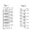
- FIG. 1is a top view showing one NAND string.
- FIG. 2is an equivalent circuit thereof.
- the NAND string depicted in FIGS. 1 and 2includes four transistors 100 , 102 , 104 and 106 in series and sandwiched between a first select gate 120 and a second select gate 122 .
- Select gate 120connects the NAND string to bit line 126 .
- Select gate 122connects the NAND string to source line 128 .
- Select gate 120is controlled by applying appropriate voltages to control gate 120 CG via selection line SGD.
- Select gate 122is controlled by applying the appropriate voltages to control gate 122 CG via selection line SGS.
- Each of the transistors 100 , 102 , 104 and 106includes a control gate and a floating gate, forming the gate elements of a memory cell.
- transistor 100has control gate 100 CG and floating gate 100 FG.
- Transistor 102includes control gate 102 CG and a floating gate 102 FG.
- Transistor 104includes control gate 104 CG and floating gate 104 FG.
- Transistor 106includes a control gate 106 CG and a floating gate 106 FG.
- Control gate 100 CGis connected to word line WL 3
- control gate 102 CGis connected to word line WL 2
- control gate 104 CGis connected to word line WL 1
- control gate 106 CGis connected to word line WL 0 .
- FIGS. 1 and 2show four memory cells in the NAND string, the use of four transistors is only provided as an example.
- a NAND stringcan have less than four memory cells or more than four memory cells.
- some NAND stringswill include eight memory cells, 16 memory cells, 32 memory cells, etc. The discussion herein is not limited to any particular number of memory cells in a NAND string.
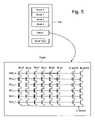
- FIG. 3shows three NAND strings 202 , 204 and 206 of a memory array having many more NAND strings.
- Each of the NAND strings of FIG. 3includes two select transistors or gates and four memory cells.
- NAND string 202includes select transistors 220 and 230 , and memory cells 222 , 224 , 226 and 228 .
- NAND string 204includes select transistors 240 and 250 , and memory cells 242 , 244 , 246 and 248 .
- Each stringis connected to the source line by one select gate (e.g. select gate 230 and select gate 250 ).
- a selection line SGSis used to control the source side select gates.
- the various NAND stringsare connected to respective bit lines by select gates 220 , 240 , etc., which are controlled by select line SGD. In other embodiments, the select lines do not necessarily need to be in common.
- Word line WL 3is connected to the control gates for memory cell 222 and memory cell 242 .
- Word line WL 2is connected to the control gates for memory cell 224 and memory cell 244 .
- Word line WL 1is connected to the control gates for memory cell 226 and memory cell 246 .
- Word line WL 0is connected to the control gates for memory cell 228 and memory cell 248 .
- a bit line and respective NAND stringcomprise a column of the array of memory cells.
- the word lines(WL 3 , WL 2 , WL 1 and WL 0 ) comprise the rows of the array. Each word line connects the control gates of each memory cell in the row. For example, word line WL 2 is connected to the control gates for memory cells 224 , 244 and 252 .
- Each memory cellcan store data (analog or digital).
- the range of possible threshold voltages of the memory cellis divided into two ranges which are assigned logical data “1” and “0.”
- the threshold voltageis negative after the memory cell is erased, and defined as logic “1.”
- the threshold voltage after a program operationis positive and defined as logic “0.”
- the threshold voltageis negative and a read is attempted by applying 0 volts to the control gate, the memory cell will turn on to indicate logic one is being stored.
- the threshold voltageis positive and a read operation is attempted by applying 0 volts to the control gate, the memory cell will not turn on, which indicates that logic zero is stored.
- a memory cellcan also store multiple levels of information, for example, multiple bits of digital data.
- the range of possible threshold voltagesis divided into the number of levels of data. For example, if four levels of information are stored, there will be four threshold voltage ranges assigned to the data values “11”, “10”, “01”, and “00.”
- the threshold voltage after an erase operationis negative and defined as “11.” Three different positive threshold voltages are used for the states of “10”, “01”, and “00.”
- a program voltageis applied to the control gate (via a selected word line) and the bit line is grounded. Electrons from the p-well are injected into the floating gate. When electrons accumulate in the floating gate, the floating gate becomes negatively charged and the threshold voltage of the cell is raised. The floating gate charge and threshold voltage of the cell can be indicative of a particular state corresponding to stored data.
- electronsare transferred from the floating gate of each memory cell to the well region and substrate.
- one or more high voltage (e.g., ⁇ 16V-20V) erase pulsesare applied to the well region to attract electrons away from the floating gate of each memory cell to the well region.
- the word lines of each memory cellare grounded or supplied with 0V to create a high potential across the tunnel oxide region to attract the electrons. If each memory cell of a NAND string is not erased after application of an erase voltage pulse, the size of the pulse can be increased and reapplied to the NAND string until each memory cell is erased.
- Typical erase operations using prior art techniquescan lead to differing erase rates amongst memory cells in a NAND string. Some memory cells may reach a target threshold voltage level for an erased state faster or slower than others. This can lead to over-erasure of faster erasing memory cells because they will continue to be subjected to erase voltages that are applied to sufficiently erase the slower memory cells of the NAND string. Thus, the different erase rates can result in a shorter cycling life of a memory cell or NAND string.
- Typical erase operationscan also lead to disparate threshold voltages among memory cells of a NAND string. That is, one or more memory cells of the NAND string may have a different threshold voltage after application of one or more erase voltage pulses when compared to other memory cells of the string or device.
- soft programminghas been used to adjust the threshold voltages of one or more memory cells after erasure.
- a relatively low program voltagelower than used for actual programming—may be applied to one or more memory cells to raise their threshold voltages in order to narrow and/or raise the threshold voltage distribution of the population of erased memory cells.
- Soft programmingmay increase program and erase times.
- the different erase ratescan result in a shorter cycling life of a memory string.
- the present inventionpertains to technology for erasing memory devices in a manner that provides a more efficient and consistent erasure of memory cells.
- a system and methodis provided that considers the individual characteristics and erase behavior of one or more memory cells of a NAND string during erase operations.
- Voltage conditions applied to selected memory cells of a non-volatile memory systemcan be changed during erase operations in order to equalize the erase behavior of the selected memory cells with other memory cells of the system that are being concurrently erased.
- the changed conditionscan compensate for capacitively coupled voltages within a NAND string. For example, after biasing a NAND string for an erase operation and beginning application of the erase voltage pulse, the word lines of one or more interior memory cells can be floated. By floating the selected interior word lines, the peak erase potential created across the tunnel dielectric region of the cells coupled thereto is decreased from its normal level. Consequently, the erase rates of these cells are slowed to substantially match that of the slower erasing end memory cells of the string. Different word lines can be floated at different times to alter the erase behavior of different memory cells by different amounts.
- the interior memory cells of a NAND stringcan be subdivided into various subsets for changing the applied voltage condition.
- a method of erasing non-volatile storageincludes applying an erase voltage to a well region of a set of non-volatile storage elements and floating a control gate of each non-volatile storage element in a subset of the set of non-volatile storage elements after beginning application of the erase voltage. Floating the control gates of the elements in the subset begins while applying the erase voltage.
- a method of erasing non-volatile storageincludes applying a first voltage signal to each non-volatile storage element in a set of non-volatile storage elements, applying an erase voltage to a well region of the set of non-volatile storage elements, and changing the first voltage signal for each non-volatile storage element in a subset of the set after beginning application of the erase voltage to the well region. Changing the first voltage signal is performed while applying the erase voltage to the well region.
- a non-volatile memory systemincludes a set of non-volatile storage elements having a well region and managing circuitry in communication with the set of non-volatile storage elements.
- the managing circuitryreceives a request to erase the set of non-volatile storage elements and responsive to the request, applies an erase voltage to the well region. After beginning application of the erase voltage, the managing circuitry floats a control gate of each non-volatile storage element in a subset of the set of non-volatile storage elements. The managing circuitry floats the control gates while applying the erase voltage.
- a non-volatile memory systemincludes a set of non-volatile storage elements having a well region and managing circuitry in communication with the set of non-volatile storage elements.
- the setincludes a first and a second subset of non-volatile storage elements.
- the first subsetis interior to the second subset.
- the managing circuitryreceives a request to erase the set and responsive to the request, applies a first voltage signal to each non-volatile storage element in the set, applies an erase voltage to the well region, and after beginning application of the erase voltage, changes the first voltage signal for each non-volatile storage element in the first subset.
- the managing circuitrychanges the first voltage signal while applying the erase voltage to the well region.
- FIG. 1is a top view of a NAND string.
- FIG. 2is an equivalent circuit diagram of the NAND string depicted in FIG. 1 .
- FIG. 3is a circuit diagram depicting three NAND strings.
- FIG. 4is a block diagram of one embodiment of a non-volatile memory system in which the various aspects of the present invention can be implemented.
- FIG. 5illustrates an exemplary organization of a memory array.
- FIG. 6depicts an exemplary program/verify voltage signal that can be applied to a selected word line in accordance with embodiments.
- FIG. 7is an exemplary flowchart for performing a program operation.
- FIG. 8depicts exemplary threshold distributions of a group of memory cells.
- FIG. 9depicts exemplary threshold distributions of a group of memory cells storing two bits of data.
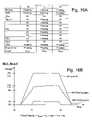
- FIG. 10is a table depicting exemplary bias conditions for performing an erase operation according to prior art techniques.
- FIG. 11is a graph depicting voltages at various portions of a NAND string during an ideal erase operation.
- FIG. 12is a cross sectional view of a NAND string depicting various capacitively coupled voltages within the NAND string.
- FIG. 13is a graph depicting various voltages of the end memory cells of a NAND string during an erase operation.
- FIG. 14depicts exemplary threshold voltage distributions of select memory cells of a NAND string after receiving an erase voltage pulse according to prior art techniques.
- FIG. 15is a graph depicting average threshold voltages of select memory cells of a NAND string as a function of an applied erase voltage pulse magnitude.
- FIG. 16Ais table depicting bias conditions for performing an erase operation according to one embodiment.
- FIG. 16Bis a graph depicting various voltages of the interior memory cells of a NAND string during an erase operation according to one embodiment.
- FIG. 17is a flowchart for erasing a NAND string in accordance with one embodiment.
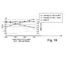
- FIG. 18is a graph depicting exemplary average threshold voltages of select memory cells of a NAND string after being erased according to one embodiment.
- FIG. 19is a timing diagram depicting various signals applied to a NAND string during an erase operation according to one embodiment and the resulting floating gate potential of the memory cells of the NAND string.
- FIG. 20is a flowchart for changing the voltage signal on selected word lines of a memory system during an erase operation according to one embodiment.
- FIG. 21is a block diagram of a row controller in accordance with one embodiment.
- FIG. 22is a graph depicting the voltage of a floated word line in one scenario.
- FIG. 23is a graph depicting the voltage of a word line that is floated then reconnected to a voltage in another scenario.
- FIG. 4is a block diagram of one embodiment of a flash memory system that can be used to implement the present invention. Other systems and implementations can be used.
- Memory cell array 302is controlled by column control circuit 304 , row control circuit 306 , c-source control circuit 310 and p-well control circuit 308 .
- Column control circuit 304is connected to the bit lines of memory cell array 302 for reading data stored in the memory cells, for determining a state of the memory cells during a program operation, and for controlling potential levels of the bit lines to promote or inhibit programming and erasing.
- Row control circuit 306is connected to the word lines to select one of the word lines, to apply read voltages, to apply program voltages combined with the bit line potential levels controlled by column control circuit 304 , and to apply an erase voltage.
- C-source control circuit 310controls a common source line (labeled as “C-source” in FIG. 6 ) connected to the memory cells.
- P-well control circuit 308controls the p-well voltage.
- the data stored in the memory cellsare read out by the column control circuit 304 and are output to external I/O lines via data input/output buffer 312 .
- Program data to be stored in the memory cellsare input to the data input/output buffer 312 via the external I/O lines, and transferred to the column control circuit 304 .
- the external I/O linesare connected to controller 318 .
- Command data for controlling the flash memory deviceis input to controller 318 .
- the command datainforms the flash memory of what operation is requested.
- the input commandis transferred to state machine 316 which is part of control circuitry 315 .
- State machine 316controls column control circuit 304 , row control circuit 306 , c-source control 310 , p-well control circuit 308 and data input/output buffer 312 .
- State machine 316can also output status data of the flash memory such as READY/BUSY or PASS/FAIL.
- Controller 318is connected to or connectable with a host system such as a personal computer, a digital camera, or personal digital assistant, etc. It communicates with the host that initiates commands, such as to store or read data to or from the memory array 302 , and provides or receives such data. Controller 318 converts such commands into command signals that can be interpreted and executed by command circuits 314 which are part of control circuitry 315 . Command circuits 314 are in communication with state machine 316 . Controller 318 typically contains buffer memory for the user data being written to or read from the memory array.
- One exemplary memory systemcomprises one integrated circuit that includes controller 318 , and one or more integrated circuit chips that each contain a memory array and associated control, input/output and state machine circuits.
- the memory systemmay be embedded as part of the host system, or may be included in a memory card (or other package) that is removably inserted into the host systems.
- a memory cardmay include the entire memory system (e.g. including the controller) or just the memory array(s) with associated peripheral circuits (with the controller or control function being embedded in the host).
- the controllercan be embedded in the host or included within the removable memory system.
- a NAND flash EEPROMis described that is partitioned into 1,024 blocks.
- the data stored in each blockcan be simultaneously erased.
- the blockis the minimum unit of cells that are simultaneously erased.
- Each blockis typically divided into a number of pages which can be a unit of programming. Other units of data for programming are also possible and contemplated.
- individual pagesmay be divided into segments and the segments may contain the fewest number of cells that are written at one time as a basic programming operation.
- One or more pages of dataare typically stored in one row of memory cells.
- FIG. 10shows four memory cells connected in series to form a NAND string. Although four cells are shown to be included in each NAND string, more or less than four can be used (e.g., 16, 32, or another number).
- One terminal of the NAND stringis connected to a corresponding bit line via a first select transistor or gate (connected to select gate drain line SGD), and another terminal is connected to c-source via a second select transistor (connected to select gate source line SGS).
- bit linesare not divided into odd and even bit lines.
- Such architecturesare commonly referred to as all bit line architectures.
- all bit lines of a blockare simultaneously selected during read and program operations. Memory cells along a common word line and connected to any bit line are programmed at the same time.
- 4,256 memory cellsare simultaneously selected.
- the memory cells selectedhave the same word line (e.g. WL 2 - i ), and the same kind of bit line (e.g. even bit lines). Therefore, 532 bytes of data can be read or programmed simultaneously. These 532 bytes of data that are simultaneously read or programmed form a logical page. Therefore, in this example, one block can store at least eight pages. When each memory cell stores two bits of data (e.g. a multi-level cell), one block stores 16 pages. Other sized blocks and pages can also be used with embodiments. Additionally, architectures other than that of FIGS. 4 and 5 can also be used to implement embodiments.
- the select gates of a selected blockare raised to one or more select voltages and the unselected word lines (e.g., WL 0 , WL 1 and WL 3 ) of the selected block are raised to a read pass voltage (e.g. 4.5 volts) to make the transistors operate as pass gates.
- the selected word line of the selected block(e.g., WL 2 ) is connected to a reference voltage, a level of which is specified for each read and verify operation in order to determine whether a threshold voltage of the concerned memory cell is above or below such level. For example, in a read operation of a one bit memory cell, the selected word line WL 2 is grounded, so that it is detected whether the threshold voltage is higher than 0V.
- the selected word line WL 2is connected to 0.8V, for example, so that as programming progresses it is verified whether or not the threshold voltage has reached 0.8V.
- the source and p-wellare at zero volts during read and verify.
- the selected bit lines (BLe)are pre-charged to a level of, for example, 0.7V. If the threshold voltage is higher than the read or verify level, the potential level of the concerned bit line (BLe) maintains the high level, because of the associated non-conductive memory cell. On the other hand, if the threshold voltage is lower than the read or verify level, the potential level of the concerned bit line (BLe) decreases to a low level, for example less than 0.5V, because of the conductive memory cell.
- the state of the memory cellis detected by a sense amplifier that is connected to the bit line and senses the resulting bit line voltage.
- the difference between whether the memory cell is programmed or eraseddepends on whether or not net negative charge is stored in the floating gate. For example, if negative charge is stored in the floating gate, the threshold voltage becomes higher and the transistor can be in enhancement mode of operation.
- the drain and the p-wellreceive 0 volts while the control gate receives a series of programming pulses with increasing magnitudes.
- the magnitudes of the pulses in the seriesrange from 12 volts to 24 volts. In other embodiments, the range of pulses in the series can be different, for example, having a starting level of higher than 12 volts.
- verify operationsare carried out in the periods between the programming pulses. That is, the programming level of each cell of a group of cells being programmed in parallel is read between each programming pulse to determine whether or not it has reached or exceeded a verify level to which it is being programmed.
- One means of verifying the programmingis to test conduction at a specific compare point.
- the cells that are verified to be sufficiently programmedare locked out, for example in NAND cells, by raising the bit line voltage from 0 to Vdd (e.g., 2.5 volts) for all subsequent programming pulses to terminate the programming process for those cells.
- Vdde.g. 2.5 volts
- the number of pulseswill be limited (e.g. 20 pulses) and if a given memory cell is not sufficiently programmed by the last pulse, an error is assumed.
- memory cellsare erased (in blocks or other units) prior to programming.
- FIG. 6depicts a program voltage signal in accordance with one embodiment.
- This signalhas a set of pulses with increasing magnitudes. The magnitude of the pulses is increased with each pulse by a predetermined step size. In one embodiment that includes the memory cells storing multiple bits of data, an exemplary step size is 0.2 volts (or 0.4 volts). Between each of the program pulses are the verify pulses.
- the signal of FIG. 6assumes a four state memory cell, therefore, it includes three verify pulses. For example, between programming pulses 330 and 332 are three sequential verify pulses.
- the first verify pulse 334is depicted at a zero volt verify voltage level.
- the second verify pulse 336follows the first verify pulse at the second verify voltage level.
- the third verify pulse 338follows the second verify pulse 336 at the third verify voltage level.
- a multi-state memory cell capable of storing data in eight statesmay need to perform verify operations at seven compare points.
- seven verify pulsesare applied in sequence to perform seven verify operations at seven verify levels between two consecutive programming pulses. Based on the seven verify operations, the system can determine the state of the memory cells.
- One means for reducing the time burden of verifyingis to use a more efficient verify process, for example, as disclosed in U.S. patent application Ser. No. 10/314,055, entitled “Smart Verify for Multi-State Memories,” filed Dec. 5, 2002; U.S. patent application Ser. No.
- FIG. 7is a flow chart describing one embodiment of a method for programming non-volatile memory.
- memory cellsare erased (in blocks or other units) and optionally soft programmed prior to programming.
- a “data load” commandis issued by controller 318 and input to command circuits 314 , allowing data to be input to data input/output buffer 312 .
- the input datais recognized as a command and latched by state machine 316 via a command latch signal, not illustrated, input to command circuits 304 .
- address data designating the page addressis input to row controller or decoder 306 from the controller or host.
- the input datais recognized as the page address and latched via state machine 316 , affected by the address latch signal input to command circuits 314 .
- a page of program data for the addressed pageis input to data input/output buffer 312 for programming. For example, 532 bytes of data could be input in one embodiment. That data is latched in the appropriate registers for the selected bit lines. In some embodiments, the data is also latched in a second register for the selected bit lines to be used for verify operations.
- a “program” commandis issued by the controller and input to data input/output buffer 312 . The command is latched by state machine 316 via the command latch signal input to command circuits 314 .
- the data latched in step 354will be programmed into the selected memory cells controlled by state machine 316 using the stepped pulses of FIG. 6 applied to the appropriate word line.
- Vpgmthe programming pulse voltage level applied to the selected word line
- a program counter PC maintained by state machine 316is initialized at 0.
- the first Vpgm pulseis applied to the selected word line. If logic “0” is stored in a particular data latch indicating that the corresponding memory cell should be programmed, then the corresponding bit line is grounded. On the other hand, if logic “1” is stored in the particular latch indicating that the corresponding memory cell should remain in its current data state, then the corresponding bit line is connected to Vdd to inhibit programming.
- the states of the selected memory cellsare verified. If it is detected that the target threshold voltage of a selected cell has reached the appropriate level, then the data stored in the corresponding data latch is changed to a logic “1.” If it is detected that the threshold voltage has not reached the appropriate level, the data stored in the corresponding data latch is not changed. In this manner, a bit line having a logic “1” stored in its corresponding data latch does not need to be programmed. When all of the data latches are storing logic “1,” the state machine knows that all selected cells have been programmed. At step 364 , it is checked whether all of the data latches are storing logic “1.” If so, the programming process is complete and successful because all selected memory cells were programmed and verified to their target states. A status of “PASS” is reported at step 366 .
- the programming processcontinues.
- the program counter PCis checked against a program limit value.
- a program limit valueis 20, however, other values can be used in various implementations. If the program counter PC is not less than 20, then it is determined at step 369 whether the number of bits that have not been successfully programmed is equal to or less than a predetermined number. If the number of unsuccessfully programmed bits is equal to or less than the predetermined number, then the programming process is flagged as passed and a status of pass is reported at step 371 . The bits that are not successfully programmed can be corrected using error correction during the read process.
- step 370If however, the number of unsuccessfully programmed bits is greater than the predetermined number, the program process is flagged as failed and a status of fail is reported at step 370 . If the program counter PC is less than 20, then the Vpgm level is increased by the step size and the program counter PC is incremented at step 372 . After step 372 , the process loops back to step 360 to apply the next Vpgm pulse.
- the flowchart of FIG. 7depicts a single-pass programming method as can be applied for binary storage.
- a two-pass programming methodas can be applied for multi-level storage, for example, multiple programming or verification steps may be used in a single iteration of the flowchart.
- Steps 358 - 372may be performed for each pass of the programming operation.
- one or more program pulsesmay be applied and the results thereof verified to determine if a cell is in the appropriate intermediate state.
- one or more program pulsesmay be applied and the results thereof verified to determine if the cell is in the appropriate final state.
- the threshold voltages of the memory cellsshould be within one or more distributions of threshold voltages for programmed memory cells or within a distribution of threshold voltages for erased memory cells.
- FIG. 8illustrates threshold voltage distributions for a memory cell array when each memory cell stores one bit of data.
- FIG. 8shows a first distribution 380 of threshold voltages for erased memory cells and a second distribution 382 of threshold voltages for programmed memory cells.
- the threshold voltage levels in the first distribution 380are negative and correspond to logic “1” while the threshold voltage levels in the second distribution 382 are positive and correspond to logic “0.”
- FIG. 9illustrates exemplary threshold voltage distributions for a memory cell array when each memory cell stores two bits of data in four physical states.
- Distribution 384represents a distribution of threshold voltages of cells that are in an erased state (storing “11”), having negative threshold voltage levels.
- Distribution 386represents a distribution of threshold voltages of cells that are in a first programmed state, storing “10.”
- Distribution 388represents a distribution of threshold voltages of cells that are in a second programmed state, storing “00.”
- Distribution 390represents a distribution of threshold voltages of cells that are in a third programmed state, storing “01.”
- Each of the two bits stored in a single memory cell, in this example,is from a different logical page.
- each bit of the two bits stored in each memory cellcarries a different logical page address.
- the bit displayed in the squarecorresponds to a lower page.
- the bit displayed in the circlecorresponds to an upper page.
- the logical statesare assigned to the sequential physical states of memory cells using a gray code sequence so that if the threshold voltage of a floating gate erroneously shifts to its nearest neighboring threshold voltage state range, only one bit will be affected.
- FIG. 3illustrates three memory cells 224 , 244 and 252 of a much larger number of cells along one word line WL 2 .
- One set of alternate cells, including cells 224 and 252store bits from logical pages 0 and 1 (“even pages”), while another set of alternate cells, including cell 244 , store bits from logical pages 2 and 3 (“odd pages”).
- Memory cellsare erased in one embodiment by raising the p-well to an erase voltage (e.g. 20 volts) and grounding or applying 0 volts to the word lines of a selected block while the source and bit lines are floating.
- FIG. 10depicts exemplary bias conditions for performing an erase operation. Due to capacitive coupling, the unselected word lines (e.g., those in unselected, not to-be-erased blocks), bit lines, select lines, and c-source are also raised to a high positive potential (e.g., 20V). A strong electric field is thus applied to the tunnel oxide layers of memory cells of a selected block and the data of the selected memory cells is erased as electrons of the floating gates are emitted to the substrate.
- an erase voltagee.g. 20 volts
- the threshold voltage of a selected cellbecomes negative. Erasing can be performed on the entire memory array, one or more blocks of the array, or another unit of cells.
- the erase voltage signal V eraseis typically applied as a series of erase voltage pulses, with an erase verification operation being carried out in between each pulse. If the unit of cells being erased is not verified as erased after application of an erase voltage pulse, another erase voltage pulse can be applied to the p-well region. In some embodiments, the peak value of the erase voltage is increased for each subsequent pulse (e.g., in 1V increments from 16V to 20V).
- FIG. 11is graph depicting the voltage at various portions of a NAND string during application of a single erase voltage pulse for a typical erase operation (e.g., under the bias condition of FIG. 10 ).
- the example of FIG. 11illustrates an ideal case, ignoring inter-gate capacitive charge coupling as discussed below.
- Curve 410depicts the voltage of the p-well region which receives erase voltage signal V erase .
- the erase voltage pulsecauses the p-well to ramp up to 20V and then back to 0V.
- Curve 414depicts the control gate voltage of a memory cell of the string.
- Curves 412 and 413depict the floating gate voltage of a non-programmed and programmed memory cell, respectively.
- the floating gate voltagedepends on the programmed state of the memory cell.
- the floating gate voltagemay be around ⁇ 1V when the memory cell is in the first programmed state (e.g., state 10 as shown in FIG. 9 ), ⁇ 2V when the memory cell is in the second programmed state (e.g., state 00 as shown in FIG. 9 ), and 0V when the memory cell is in a non-programmed state.
- the control gate voltage 414remains at 0V throughout the erase operation while the floating gate voltages 412 and 413 rise in proportion to the p-well voltage.
- the floating gateis capacitively coupled across the tunnel dielectric region to the p-well.
- the capacitive coupling ratio between the floating gate of a memory cell and the p-well regionis about 40-50%. Accordingly, floating gate voltage 412 rises in about a 0.5:1 ratio (when the coupling ratio is 50%) with the p-well voltage to a voltage of about 10V and floating gate voltage 413 rises to about 8V.
- the resulting erase potentialthe potential between the cell's floating gate and the p-well region at the beginning of the erase voltage pulse, is given below the graph of FIG. 11 .
- the erase potentialis equal to about 10V at the beginning of the first erase voltage pulse for the non-programmed cell ( 412 ) and 12V for the cell having a starting floating gate voltage of ⁇ 2V ( 413 ).
- the erase potentialchanges during the actual erase voltage pulse as electrons are transferred from the floating gate to the p-well.
- the floating gate voltagewill be different than before the erase voltage pulse was applied.
- the floating gate voltagewill be positive after the first erase voltage pulse, corresponding to a negative (erased) threshold voltage of the memory cell.
- FIG. 12provides a cross-sectional view of a NAND string including 8 memory cells. Although embodiments are presented with respect to FIG. 12 and an 8 cell NAND structure, the present invention is not so limited and can be used in accordance with numerous NAND structures including fewer or more than 8 memory cells (e.g., 4, 12, 16, or more). As depicted in FIG. 12 , the memory cells of the NAND string are formed in p-well region 540 .
- Each memory cell( 502 , 504 , 506 , 508 , 510 , 512 , 514 , and 516 ) includes a stacked gate structure that consists of the control gate ( 502 c , 504 c , 506 c , 508 c , 510 c , 512 c , 514 c , and 516 c ) and a floating gate ( 502 f , 504 f , 506 f 510 f , 512 f , 514 f , and 516 f ).
- the floating gatesare formed on the surface of the p-well on top of an oxide or other dielectric composite film.
- the control gateis above the floating gate, with an oxide or other isolating dielectric layer separating the control gate and floating gate.
- the control gates of the memory cellsconnect to or form word lines WL 0 , WL 1 , WL 2 , WL 3 , WL 4 , WL 5 , WL 6 , and WL 7 .
- N+ diffused regions 542are shared between neighboring cells whereby the cells are connected to one another in series to form a NAND string. These N+ diffused regions form the source and drain of each of the cells.
- N+ diffused region 526connects to the bit line for the NAND string, while N+ diffused region 528 connects to a common source line for multiple NAND strings.
- the select gates 520 and 522are formed of the same structure as the memory cells, however, the gate regions are electrically connected.
- the floating select gates 522 and 520are raised to a high positive potential when a high erase voltage is applied to the p-well during erase operations.
- the erase voltage applied to the p-well, or some portion thereofcouples from the well region to each of the select gates. About 90-100% of the p-well voltage can be expected to couple to each select gate in many NAND structures. Therefore, if an erase voltage pulse of 20V is applied to the p-well, the voltage on each select gate will rise about 18V-20V to a voltage of 18V-20V.
- the coupling from p-well 540 to select gates 522 and 520is illustrated by arrows 530 .
- each floating gateis also coupled to its corresponding control gate with a coupling of about 50-60%. To a smaller extent, each floating gate is coupled to neighboring floating gates and control gates. All the different couplings add up to a total of 100%. Assuming a 50% coupling from p-well to floating gate, the floating gate voltage of each memory cell is raised about 10V under application of a 20V erase voltage pulse. This coupling effect is illustrated by arrows 532 . The voltage coupled to each memory cell's floating gate effects the V erase potential created across the tunnel oxide layer. For example, an erase potential of about 10V (20V ⁇ 10V) is created under application of a 20V erase voltage pulse to the p-well for a memory cell having a floating gate voltage of 0V prior to erasing.
- Each memory cell of the stringwill experience some capacitive charge coupling from neighboring memory cells and/or transistors. This coupling can effect the potential of a cell's floating gate and consequently, the erase potential for the cell.
- this capacitive couplingis depicted by arrow 534 from select gate 520 to floating gate 502 f of memory cell 520 and by arrow 538 from select gate 522 to floating gate 516 f of memory cell 516 .
- the voltage coupled to memory cells 502 and 516will decrease the electric field present across those cells' tunnel dielectric regions (e.g., tunnel oxide) in proportion to the amount of voltage at the respective select gate.
- the coupling represented by arrows 538 and 534occurs in both directions because during an erase operation, the select gates are in a floating state as well. As a result, the floating gate voltage of memory cells 516 and 502 will have some influence on the voltage on the select gates 522 and 520 . However, the coupling from floating gate to select gate is much smaller than the coupling from the p-well to the select gates, and thus, the select gate voltage is determined almost completely by the p-well voltage.
- capacitive coupling from the select gates to the floating gates of the end memory cells of a NAND stringcan be expected to be on the order of about 2% to 5%. If an erase voltage of 20 volts is applied to the p-well region, each select gate's voltage will rise about 18V with 90% p-well to select gate coupling. Subsequently, due to the 2-5% coupling from select gate to neighboring floating gate, the voltage on the neighboring floating gates (e.g., 516 f and 502 f ) will rise about 0.4-1V. The resulting voltage across the tunnel oxide of the end memory cells of the string will be about 0.4V to 1V less than that for the ideal case shown in FIG. 11 .
- the above mentioned capacitive couplingcan vary largely depending on the physical dimensions of the memory cells and select gates, the spacing between memory cells and select gates, and the dielectric properties of the materials used in constructing such components as the tunnel dielectric, dielectric between control and floating gates, and dielectric between select gates and memory cells. In some cases, for example, the above mentioned coupling may be larger or smaller than the above mentioned 2-5% range.
- the floating gate and neighboring word lines or control gatesare coupled to the floating gate and neighboring word lines or control gates.
- This couplingmay also be on the order of 2-5%, but may be smaller or larger depending on the dimensions and shape of the memory cells.
- the coupling from the select gate to the neighboring floating gatewill be in a similar range as the coupling from a neighboring control gate (word line) and floating gate.
- the select gateis biased differently in comparison with the control gates and floating gates, the floating gate voltage of the end memory cells will be higher than that of the interior memory cells and thus, the erase potential will be lower for the end memory cells as hereinafter described.
- FIG. 13depicts the p-well voltage 420 , floating gate voltage 422 , and control gate voltage 424 for a typical end memory cell of a NAND string during application of a single erase voltage pulse for an erase operation under the bias conditions of FIG. 10 . It is assumed that the floating gate voltage is 0V prior to application of the erase voltage pulse. The p-well voltage 420 rises from 0V to a peak value of 20V and then back to 0V. The control gate voltage 424 remains at 0V since the word lines connected to each memory cell are supplied with 0V. As with all the cells, the floating gates of the end memory cells are capacitively coupled to the p-well region on the order of about 40-50%.
- the erase potential across the tunnel dielectric region for the end memory cellsis given below the graph of FIG. 13 .
- the erase potential at the beginning of the erase voltage pulseis about 9V, or about 1V less than the 10V erase potential for the ideal case. If the floating gate voltage had been ⁇ 2V prior to the erase voltage pulse, the floating gate voltage would rise to 9V, resulting in an erase potential of about 11V for the end memory cell, compared to the corresponding erase potential of 12V for an ideal memory cell having a starting floating gate voltage of ⁇ 2V, as shown in FIG. 11 (curve 413 ).
- the memory cells of a NAND string that are not adjacent to a select gatemay be referred to herein as interior memory cells of the string.
- the interior memory cells of the NAND stringare memory cells 504 , 506 , 508 , 510 , 512 , and 514 .
- the interior memory cellswill experience capacitive coupling from neighboring floating gates that will decrease their erase potential (discussed hereinafter), it is of a lesser degree than that of the end memory cells.
- the interior memory cellswill behave substantially as the ideal case described earlier and have an erase potential of 10V (assuming that the cells were in an non-programmed state with a floating gate voltage of about 0V before the erase voltage pulse). Because of the lower potential across the tunnel oxide layers of the end memory cells compared to the interior memory cells, the end memory cells will erase slower and not be as deeply erased (will have fewer electrons transferred from their floating gates) as the interior memory cells after application of one or more erase voltage pulses.
- Memory cells of a NAND stringare verified as erased when the charge on the floating gate is above a predetermined level (threshold voltage below a predetermined level). Because of the additional coupling to the floating gates of the end memory cells, the overall time for an erase operation is increased in order to sufficiently erase these end memory cells.
- the interior memory cellsmay be sufficiently erased after application of a number N erase voltage pulses, while the end memory cells of the NAND string may not be sufficiently erased until application of N+1 or more erase voltage pulses.
- FIG. 14depicts the threshold voltage distributions of a set of memory cells after application of a single erase voltage pulse (a similar distribution with lower overall V T values may exist after multiple erase voltage pulses).
- Distribution 430depicts the threshold voltage distribution for the interior memory cells of a NAND string, such as the memory cells connected to WL 1 -WL 6 in FIG. 12 .
- Distribution 432depicts the threshold voltage distribution for the end memory cells, such as those connected to WL 0 and WL 7 in FIG. 12 . As illustrated, those memory cells connected to the interior word lines are deeper erased than the memory cells of the end word lines after application of just one erase voltage pulse. In some NAND memory device implementations, the interior memory cells can be expected to be about 0.5-1V deeper erased than the end memory cells in the example shown.
- the average threshold voltage of the interior memory cellsis lower than that of the end word lines because the number of electrons transferred from the floating gates of those memory cells is more than that of the memory cells connected to the end word lines.
- the memory cells of both the interior and end word linesare in general erased deeper than required.
- the selected size of the first erase voltage pulseis generally larger than required to erase all the cells of a fresh device (not having undergone many write/erase cycles) in one pulse.
- a fresh memory devicemay have threshold voltage distributions as shown in FIG. 14 after undergoing an erase operation.
- FIG. 15is a graph depicting the average threshold voltage of the memory cells of a NAND string as a function of an applied erase voltage signal.
- a 16V erase voltage pulsethe average threshold voltage of a memory cell connected to WL 0 or WL 7 is almost ⁇ 1V.
- the average threshold voltage of the interior memory cells, those memory cells connected to WL 1 -WL 6is about ⁇ 1.5V.
- the average threshold voltage for WL 0 and WL 7has decreased to about ⁇ 1.5V while the average threshold voltage of the memory cells connected to WL 1 -WL 6 is about ⁇ 2.8V.
- the difference between the average threshold voltage of the interior memory cells and the end memory cellsincreases. This effect is illustrated by the third line (Delta V t ) in FIG. 15 which depicts the difference in average threshold voltage between the interior memory cells and the end memory cells after each erase voltage pulse.
- the interior memory cells of a NAND stringmay be over erased while attempting to sufficiently erase the end memory cells of the string. As previously described, the interior memory cells will erase faster than the end memory cells. If verification is performed at a NAND string level, the NAND string will continue to receive an erase voltage pulse at the p-well until each memory cell of the string is erased. Therefore, even though the interior memory cells may sufficiently erase after a lower number of erase voltage pulses than the end memory cells, the interior memory cells will receive additional erase voltage pulses until each memory cell of the string is verified as erased.
- a greater stressis placed on the interior memory cells than is necessary because of over erasure. Over erasing the interior memory cells because of the slower erase times of the end memory cells can decrease the life span of the interior memory cells and an overall non-volatile memory system.
- application of a large potential across the tunnel oxide layer of a transistorstresses the oxide material.
- Application of a high enough potential across the tunnel oxide layer or application of a lower potential a number of timescan eventually lead to a breakdown of the oxide layer.
- Disparate erase behavior between memory cellscan also lead to increased erase operation times because of additional operations that may be performed to change the threshold voltage of a memory cell after being erased.
- the goalis that all erased cells have a negative threshold voltage within a predefined range of negative threshold voltages.
- the erase processmay result in some cells having negative threshold voltages below the predefined range.
- Memory cells having a threshold voltage that is too lowmay not subsequently program properly or may cause other cells to not program properly (e.g., by increasing the probability that program disturb occurs).
- over-erased deviceswill often undergo what is called soft programming.
- Memory cells with threshold voltages of significantly lower values within the predefined rangewill receive a small amount of programming so that the threshold voltage is raised to be within the predefined range.
- the soft program processrequires an additional operation to be performed and decreases memory performance due to increased erase times as soft programming is usually considered part of the erase operation.
- the voltage condition applied to select memory cells of a NAND stringis changed after applying the erase voltage to the p-well region during an erase operation.
- those selected memory cellscan have their erase behavior adjusted to substantially match that of other memory cells of the NAND string.
- 0Vis applied to each word line of the NAND string.
- An erase voltage pulseis then applied to the p-well region.
- the voltage condition for the interior memory cellscan be changed so that they erase slower.
- the conditioncan be changed so that the erase rate of the interior memory cells substantially matches the erase rate of the end memory cells.
- changing the voltage condition for a memory cellcan include floating the word line to which it is connected so that no electrical connection is provided thereto.
- FIG. 16Adepicts the bias conditions of a technique in accordance with one embodiment for slowing down the erase rate of select memory cells to match that of other memory cells in the NAND string.
- FIG. 16Bdepicts the p-well voltage 440 , floating gate voltage 446 , and control gate voltage 448 of an interior memory cell during application of a single erase voltage pulse using these bias conditions. It is again assumed that the starting floating gate voltage of the memory cell is 0V. The voltages for the end memory cells will be the same as shown in FIG. 13 .
- the NAND stringis biased to begin the erase.
- the p-well voltage 440subsequently rises from 0V to 20V and then decreases back to 0V.
- the interior word linesare at 0V until time t 1 so the control gate voltage 446 remains at 0V until time t 1 .
- the floating gate voltage 448rises to 9V from time t 0 to t 1 (assuming 50% coupling to the p-well) which climbs to 18V during that time.
- the control gates of the interior memory cellsare floated by floating the word lines to which they are connected. With the word lines floating, the control gates become strongly coupled to the p-well through the floating gates. In turn, the floating gates become much more capacitively coupled to the p-well region.
- the control gate and floating gate of a cellWith the word line floating, the control gate and floating gate of a cell will be about 100% capacitively coupled to the p-well.
- the floating gate voltage for each of the interior memory cellswill begin to rise in a 1:1 ratio with that of the p-well voltage.
- the floating gate voltageswill also increase by 2V to a value of 11V.
- the control gate voltages 448will rise to 2V from 0V once the world lines are floating.
- the interior memory cells' floating gatesare made to rise an additional 1V over that which would be achieved were the word lines to remain at 0V as in a typical operation.
- each memory cell of the NAND stringwill have a consistent potential of 9V created across its tunnel dielectric region.
- the effectswill be the same. For example, a memory cell having a starting floating gate voltage of ⁇ 1V will have its floating gate voltage rise to 8V at time t 1 , and then rise an additional 2V until the time the p-well voltage reaches its peak value. This will create a 10V erase potential (20V ⁇ 10V), which is the same erase potential achieved for an end memory cell having a starting floating gate voltage of ⁇ 1V.
- each interior word lineis again supplied with 0V at time t 2 to reduce the capacitive coupling between the p-well region and the floating gate.
- the control gate voltage 448will return to 0V.
- the floating gate voltage 446will now track the decrease in the p-well voltage according to the 50% coupling ratio, rather than the 100% coupling ratio.
- Reapplying 0V to the interior word lines at time t 2is not necessary in all embodiments.
- the word linesare again applied with 0V so that a large voltage is not present at any transistors within the row controller for the device. In certain implementations this may not be necessary.
- the time at which 0V is again applied to the word linecan vary by embodiment. More details regarding reapplying 0V to the interior word lines will be described with respect to FIGS. 21-23 .
- changing the voltage condition for the interior word linesincludes applying a positive compensation voltage to the interior word lines to slow down the erase rate of the interior memory cells.
- a positive compensation voltageto the interior word lines to slow down the erase rate of the interior memory cells.
- the end word linescan have their voltage condition changed to speed up their erase rates. In this case, a negative compensation voltage can be applied to the end word lines.
- FIG. 17is a flow chart in accordance with one embodiment for erasing a NAND string where the voltage condition for select memory cells is changed during the operation to equalize the erase behavior of those cells with other memory cells of the NAND string.
- FIG. 17will be described in terms of a single NAND string, it will be understood by one of ordinary skill in the art that operation of a flow chart can be performed, such as in parallel, on multiple NAND strings in order to erase a larger unit of memory cells (e.g., one or more blocks).
- the bit, source, source select gate, and drain select gate lines of the NAND stringare floated.
- 0Vis applied to each word line of the NAND string.
- an erase voltage pulseis applied to the p-well region of the NAND string.
- the voltage signal applied to the interior word lines of the NAND stringis changed. The signal is changed prior to the erase voltage pulse reaching its peak value to lower the resulting erase potential.
- Step 466can include floating the word lines of the interior memory cells so that their floating gates are capacitively coupled to the p-well region. Floating the word lines will effectively limit the potential created between these cells' floating gates and the p-well to the level it is at when the lines are floated.
- 0Vis reapplied to the interior word lines. As previously described, step 468 may not be necessary in all embodiments.
- Verificationis performed at step 470 to determine whether the NAND string has been sufficiently erased.
- Numerous meanscan be used in accordance with embodiments to verify the results of an erase operation.
- the NAND stringmay be read in order to determine that the threshold voltage of each of the memory cells of the string is below a specified value. In one embodiment, this can include applying a voltage sufficient to turn on an erased memory cell to the gate of each memory cell and testing conduction of the NAND string in a direction such as from the source to bit line. More details regarding erase and erase verification can be found in co pending U.S. patent application Ser. No. 10/857,245, entitled “COMPREHENSIVE ERASE VERIFICATION FOR NON-VOLATILE MEMORY,” incorporated herein by reference in its entirety, which describes a more comprehensive erase verification technique.
- a status of passis reported for the NAND string at step 474 . If, however, it is not determined that the NAND string is sufficiently erased at step 472 , a verify counter is checked against a predetermined value at step 476 . If the verify counter is less than the predetermined value (e.g., 20) then the erase voltage pulse level (V erase ) is incremented by a predetermined value and the verify counter is increased by 1 at step 478 . Operation of the flow chart then continues to step 460 to set the NAND string up for application of an additional erase voltage pulse having the increased peak value. If the verify counter is greater than the predetermined number at step 476 , a status of fail is reported for the NAND string at step 477
- FIG. 18is a graph depicting the average threshold voltage of the memory cells of a NAND string, such as depicted in FIG. 12 , when utilizing a changing voltage condition as described in FIGS. 16 and 17 .
- the actual values depicted in FIG. 18are exemplary only and do not necessarily correspond to the examples previously discussed.
- the graphdepicts the threshold voltage (Y axis) as a function of the value of V erase when the interior word lines are floated (X axis).
- Word lines WL 0 and WL 7remain at 0V in each scenario and thus exhibit a near constant voltage regardless of when the interior memory cells are floated.
- the average threshold voltage of the memory cells of WL 0 and WL 7is about ⁇ 1.5 volts.
- the average threshold voltage of the interior memory cells after application of a single erase voltage pulseis about ⁇ 2.6 volts. If the interior word lines are floated when V erase is 19V (thus decreasing the erase potential for the interior memory cells by 0.5V), the average threshold voltage for the memory cells of WL 1 -WL 6 increases after application of the erase voltage pulse to about ⁇ 2 volts. The average threshold voltage for the memory cells of WL 1 -WL 6 continues to increase by floating the interior word lines sooner (i.e., when V erase is smaller).
- the interior word linesare floated when V erase , equals 18V (thus decreasing the erase potential by 1V), the average threshold voltage is increased to about ⁇ 1.5V. This is the same value for the end memory cells of the NAND string. Thus, if the interior word lines are floated when V erase equals 18V, they will erase at about the same rate as the end memory cells of the NAND string. If the interior word lines are floated any sooner (when V erase is even smaller), the interior memory cells will begin to erase slower than the end memory cells.
- FIG. 12illustrates an additional capacitive coupling effect between the floating gates of individual memory cells of the NAND string by arrows 536 .
- the coupling between neighboring floating gates on WL 0 and WL 1may be on the order 2-5%, but may be smaller or larger depending on the dimension and shape of the memory cells.
- a voltage present on the floating gate of memory cell 516will influence the voltage of the floating gate of memory cell 514 and vice versa.
- a similar coupling effectwill be present between the floating gates of memory cells 514 and 512 , connected to WL 2 , and so on. This coupling exists in both directions, as indicated by the double head on arrows 536 . These coupling effects will be seen among all memory cells of the NAND string at various levels but the impact of the coupling will be less than that on the end memory cells as the bias voltages on the neighboring control gates and floating gates are different from the bias condition on the select gates. During the presence of the erase voltage pulse, the voltage of each floating gate is significantly less than the voltage present at the select gates.
- each memory cell of the NAND stringcan be expected to have a slightly differing net charge present at its floating gate and a correspondingly different erase behavior due to such coupling.
- the interior memory cells or word lines of a NAND stringare divided into subsets of one or more memory cells.
- the individual subsets of the interior memory cellswill have the voltage signal applied thereto changed at differing times in order to further normalize the erase behavior of each of these memory cells.
- the end memory cellswill have about 2-5% of the voltage at the select gate ( ⁇ V erase peak value) coupled to them.
- the cells adjacent to the end memory cellswill have about 2-5% of this coupled voltage coupled to them, and so on.
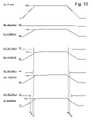
- FIGS. 19A-19Idepict a method in accordance with one embodiment for floating the interior word lines of a NAND string at different times in order to normalize the erase behavior of each interior memory cell to match that of the end memory cells.
- FIG. 19Adepicts the p-well voltage which rises from 0V to 20V in accordance with the erase voltage V erase .
- FIGS. 19D and 19Edepict the voltage signal applied to word lines WL 1 and WL 6 , and the resulting floating gate voltages for the memory cells connected to these word lines.
- Word lines WL 1 and WL 6are immediately adjacent to word lines WL 0 and WL 7 , respectively.
- the memory cells at WL 1 and WL 6will have the largest positive charge at their floating gate and thus, need the least amount of compensation in order to substantially match the end memory cells.
- WL 1 and WL 6are floated at time t 3 which is just before the erase voltage pulse reaches its peak value.
- these word linesmay be floated when the p-well and V erase are at 19V.
- FIG. 19Ethis results in the floating gate potential for the memory cells at WL 1 and WL 6 rising to the same level as that of the memory cells at WL 0 and WL 7 , namely 11 volts.
- FIGS. 19F and 19Gdepict the voltage signal applied to WL 2 and WL 5 , and the resulting floating gate voltages for the memory cells connected to them. Because these word lines are interior to WL 2 and WL 6 and have less positive charge at their memory cells' floating gates, they need to be floated earlier to gain the additional capacitive coupling effect for a longer period of time.
- Word lines WL 2 and WL 5are floated at time t 2 , preceding time t 3 .
- time t 2may correspond to the time of which the p-well and V erase reach 18V. As shown in FIG. 19G , this results in the floating gate voltage of the memory cells at WL 2 and WL 5 climbing from 0V to 11V. By floating the word lines of these memory cells at time t 2 , their erase behavior has been made to match that of the end memory cells.
- FIGS. 19H and 19Idepict the voltage signal applied to word lines WL 3 and WL 4 , and the resulting floating gate voltages for the memory cells connected to them.
- WL 3 and WL 4are the most interior word lines of the NAND string. Because they are farthest from the select gates, the charge coupled to their floating gates is the smallest. Because these memory cells have the smallest amount of positive charge coupled to their floating gate, their word lines must be floated for an even longer period of time in order to normalize their erase behavior with that of the end memory cells. Accordingly, WL 3 and WL 4 are floated at time t 1 , preceding both times t 2 and t 3 . For example, time t 3 may correspond to the time when the p-well and V erase reach 17V. By floating these word lines at time t 1 . The resulting floating gate voltage for the memory cells at WL 3 and WL 4 will rise from 0V to 11V to match that of the end memory cells.
- times t 1 , t 2 , t 3 , etc., for any given NAND string implementationcan be selected based on the design of that implementation.
- the erase voltages and coupling effectswill vary in different implementations. Thus, these times will differ by embodiment. However, in each case the more interior a memory cell is, the sooner its corresponding word line should be floated in order to normalize the erase behavior of the memory cell with that of the end memory cells.
- FIGS. 19A through 191also depict times t 4 , t 5 , t 6 in which 0V is again applied to each of the word lines. As previously described, reapplying 0V to the word lines may not be necessary in each embodiment.
- each subset of word linesis reconnected to 0V at a time corresponding to when it was allowed to float.
- each of the word lines of all interior memory cellscan be reconnected to 0V at the same time or they can be reconnected at different times and in different orders than that depicted in FIG. 19 . More details will be described in FIGS. 21-23 .
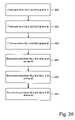
- FIG. 20is a flow chart in accordance with one embodiment where the interior word lines are divided into subsets which are floated at differing times in order to more precisely normalize their erase behavior with that of the end memory cells. It will be appreciated by those of ordinary skill in the art that the example presented in FIG. 20 is for exemplary purposes only and that other embodiments will include NAND strings having more or fewer word lines and that other configurations of the steps herein can be made.
- FIG. 20corresponds to steps 466 and 468 of FIG. 17 .
- Steps 480 through 484correspond to step 466 where the voltage signal of the interior word lines is changed
- steps 486 though 490correspond to step 468 where the interior word lines are reconnected to 0V.
- the most interior word linesare floated.
- word lines WL 3 and WL 4are floated at time t 1 .
- the next most interior word linesare floated.
- word lines WL 2 and WL 5are floated at time t 2 .
- the next most interior word linesare floated.
- More or less than 2 word linescan be grouped together as a subset for having their word line floated at a particular time.
- word lines WL 3 , WL 4 , WL 2 and WL 5can be grouped together in one subset and floated at the same time.
- step 480will include floating word lines WL 2 , WL 3 , WL 4 , and WL 5 , all at time t 1 .
- Step 482 in such an examplewould not exist and at the next time period, word lines WL 1 and WL 6 would be floated.
- word lines WL 2 , WL 5 , WL 1 , and WL 6could be grouped together.
- numerous subdivisions of the interior word linescan be made. For example, in a 16 memory cell NAND string having word lines WL 0 through WL 15 , the interior word lines (WL 1 -WL 14 ) could be subdivided into two subsets.
- the first subsetcan include the most interior word lines (for example, WL 4 -WL 11 ), and the second subset can include the less interior word lines (WL 1 -WL 3 and WL 12 -WL 14 ).
- WL 4 -WL 11would be floated at a first time and WL 1 -WL 3 and WL 12 -WL 14 would be floated at a second later time.
- Different subsetscould also be made.
- each of the 14 word linescan be floated individually at individual times, or the word lines can be grouped together in pairs (for example, WL 1 -WL 14 , WL 2 -WL 13 , etc.) and each group have its word lines floated at a particular time.
- step 486time t 4
- WL 1 and WL 6are reconnected to zero volts.
- step 488time t 5
- WL 2 and WL 5are reconnected to 0V
- step 490time t 6
- steps 486 through 490may not be necessary in all embodiments.
- the time at which each word line is reconnected to zero voltscan vary be embodiment.
- FIGS. 21 through 23illustrate reconnecting a word line to 0V after allowing it to float. Such a step is not necessary in all embodiments. In certain implementations, however, reconnecting the word line to a voltage such as 0V may be necessary in order not to avoid damage to a transistor within the memory system.
- FIG. 21depicts one embodiment of row controller 306 .
- Row controller 306includes a control gate driver 608 and three word line switch gates 602 , 604 , 606 .
- FIG. 21depicts only a portion of the row controller.
- a switch gatemay be present for each word line of the system. Each switch gate 602 , 604 , and 606 is responsible for supplying the appropriate voltages to the word lines doing various operations.
- control gate driver 608can cause the control gate driver line of a switch gate (for example CGD n ⁇ 2 ) to float. By floating the control gate driver line, the word line connected to the corresponding switch gate will also float.
- FIG. 22depicts the word line voltage of a word line that is floated at time t 1 and allowed to continue floating throughout application of an erase voltage pulse.
- the word lineWhen the word line is floated at time t 1 it becomes coupled to the floating gate which in turn is strongly coupled to the p-well region.
- the word line voltagewill rise by the increase in the p-well voltage from the moment of allowing the word line to float. If the word line is allowed to float at time t 1 , when the p-well voltage is 18V, and the p-well voltage climbs to 20V thereafter, the word line voltage will rise to 2V.
- FIG. 22depicts the word line voltage of a word line that is floated at time t 1 and allowed to continue floating throughout application of an erase voltage pulse.
- the word lineWhen the word line is floated at time t 1 it becomes coupled to the floating gate which in turn is strongly coupled to the p-well region.
- the word line voltagewill rise by the increase in the p-well voltage from the moment of
- time t 2is the time at which the p-well voltage begins to decrease from its peak value of 20V. Because the word line is coupled to the p-well through the control and floating gates, its voltage will decrease in a 1:1 ratio with the decrease in the p-well voltage. Accordingly, the word line voltage will decrease from 2V to ⁇ 18V. This large negative voltage on the word line will be seen at the source end of switch gate 602 . If a very large negative voltage is present on WL n ⁇ 2 , switch gate 602 can begin to leak current, resulting in damage to switch gate 602 .
- a word line that is floated during application of an erase voltage pulseis reconnected to 0V in order to avoid this condition from occurring.
- FIG. 23illustrates such an example.
- the word lineis floated at time t 1 .
- the word lineis reconnected to 0V at time t 3 .
- Time t 3can correspond to the time at which the erase voltage pulse has decreased from its peak value of 20V to 18V. Because of the decrease of 2 volts, the word line voltage will have decreased from 2V to 0V. At this time, the word line is reconnected to 0V so that it will remain at 0V thereafter.
- the voltage at the source of select gate 602 for examplewill remain at 0V and not damage the gate.
- the word linecan be reconnected to 0V or another voltage.
- the timedoes not have to correspond to the time of floating so long as the high negative voltage is avoided, numerous variations can be made.
- the word line switch gate signalremains at VDD throughout application of the erase voltage pulse.
- control gate driver 608will supply 0V to the control gate driver line (e.g., CGD n ⁇ 2 ). In this manner, 0V will be provided on word line WLN- 2 and no damage will be seen at the select gate.
- control gate driver 608can provide a voltage on the control gate driver line that is greater than VDD rather than allowing the control gate driver line to float. This will also result in the word line floating if the control gate driver line voltage is larger than that provided by the switch gate signal.
- row controller 306may include individual word line switch gate signals for each select gate.
- 0Vcan be supplied to a word line by control gate driver 608 providing 0V on the control gate driver line and the word line switch gate signal providing a voltage equal to VDD. This will result in the word line that is connected to the switch gate being at 0V. In such an embodiment, it is not necessary to float or provide a voltage greater than VDD to the control gate driver line. By supplying 0V to the gate of the select gate, the word line is forced to float. Thereafter, in order to reconnect the word line to 0V, the switch gate signal can again be driven with VDD in order to turn on the select gate transistor and provide 0V to the word line.
Landscapes
- Engineering & Computer Science (AREA)
- Microelectronics & Electronic Packaging (AREA)
- Computer Hardware Design (AREA)
- Read Only Memory (AREA)
Abstract
Description
Claims (40)
Priority Applications (9)
| Application Number | Priority Date | Filing Date | Title |
|---|---|---|---|
| US11/295,755US7430138B2 (en) | 2005-03-31 | 2005-12-06 | Erasing non-volatile memory utilizing changing word line conditions to compensate for slower erasing memory cells |
| DE602006012170TDE602006012170D1 (en) | 2005-03-31 | 2006-03-29 | DELETE A NON-VOLATILE MEMORY USING MODIFIED WORDING CONDITIONS TO COMPENSATE SLOWING MEMORY CELLS |
| KR1020077023541AKR100909720B1 (en) | 2005-03-31 | 2006-03-29 | How to erase nonvolatile memory by changing wordline conditions to compensate for slow erase memory cells |
| CN2006800099947ACN101199024B (en) | 2005-03-31 | 2006-03-29 | Erasing non-volatile memory using changing word line conditions to compensate for slower erasing memory cells |
| PCT/US2006/011651WO2006124122A2 (en) | 2005-03-31 | 2006-03-29 | Erasing non-volatile memory utilizing changing word line conditions to compensate for slower frasing memory cells |
| EP06784329AEP1864292B1 (en) | 2005-03-31 | 2006-03-29 | Erasing non-volatile memory utilizing changing word line conditions to compensate for slower frasing memory cells |
| JP2008504364AJP4762305B2 (en) | 2005-03-31 | 2006-03-29 | A method for erasing a non-volatile memory using a word line change condition to correct a memory cell having a low erasing speed |
| AT06784329TATE457518T1 (en) | 2005-03-31 | 2006-03-29 | ERASING NON-VOLATILE MEMORY USING VARIABLE WORD LINE CONDITIONS TO COMPENSATE FOR SLOW-WRITE MEMORY CELLS |
| TW095111549ATWI319878B (en) | 2005-03-31 | 2006-03-31 | A method of erasing non-volatile storage and a non-volatile memory system |
Applications Claiming Priority (2)
| Application Number | Priority Date | Filing Date | Title |
|---|---|---|---|
| US66704305P | 2005-03-31 | 2005-03-31 | |
| US11/295,755US7430138B2 (en) | 2005-03-31 | 2005-12-06 | Erasing non-volatile memory utilizing changing word line conditions to compensate for slower erasing memory cells |
Publications (2)
| Publication Number | Publication Date |
|---|---|
| US20060221708A1 US20060221708A1 (en) | 2006-10-05 |
| US7430138B2true US7430138B2 (en) | 2008-09-30 |
Family
ID=39548400
Family Applications (7)
| Application Number | Title | Priority Date | Filing Date |
|---|---|---|---|
| US11/296,055Active2026-08-01US7403424B2 (en) | 2005-03-31 | 2005-12-06 | Erasing non-volatile memory using individual verification and additional erasing of subsets of memory cells |
| US11/296,071ActiveUS7408804B2 (en) | 2005-03-31 | 2005-12-06 | Systems for soft programming non-volatile memory utilizing individual verification and additional soft programming of subsets of memory cells |
| US11/296,032ActiveUS7403428B2 (en) | 2005-03-31 | 2005-12-06 | Systems for erasing non-volatile memory utilizing changing word line conditions to compensate for slower erasing memory cells |
| US11/295,755Active2026-12-23US7430138B2 (en) | 2005-03-31 | 2005-12-06 | Erasing non-volatile memory utilizing changing word line conditions to compensate for slower erasing memory cells |
| US11/296,028ActiveUS7400537B2 (en) | 2005-03-31 | 2005-12-06 | Systems for erasing non-volatile memory using individual verification and additional erasing of subsets of memory cells |
| US11/295,747Active2027-03-19US7486564B2 (en) | 2005-03-31 | 2005-12-06 | Soft programming non-volatile memory utilizing individual verification and additional soft programming of subsets of memory cells |
| US12/040,632ActiveUS7606100B2 (en) | 2005-03-31 | 2008-02-29 | Erasing non-volatile memory using individual verification and additional erasing of subsets of memory cells |
Family Applications Before (3)
| Application Number | Title | Priority Date | Filing Date |
|---|---|---|---|
| US11/296,055Active2026-08-01US7403424B2 (en) | 2005-03-31 | 2005-12-06 | Erasing non-volatile memory using individual verification and additional erasing of subsets of memory cells |
| US11/296,071ActiveUS7408804B2 (en) | 2005-03-31 | 2005-12-06 | Systems for soft programming non-volatile memory utilizing individual verification and additional soft programming of subsets of memory cells |
| US11/296,032ActiveUS7403428B2 (en) | 2005-03-31 | 2005-12-06 | Systems for erasing non-volatile memory utilizing changing word line conditions to compensate for slower erasing memory cells |
Family Applications After (3)
| Application Number | Title | Priority Date | Filing Date |
|---|---|---|---|
| US11/296,028ActiveUS7400537B2 (en) | 2005-03-31 | 2005-12-06 | Systems for erasing non-volatile memory using individual verification and additional erasing of subsets of memory cells |
| US11/295,747Active2027-03-19US7486564B2 (en) | 2005-03-31 | 2005-12-06 | Soft programming non-volatile memory utilizing individual verification and additional soft programming of subsets of memory cells |
| US12/040,632ActiveUS7606100B2 (en) | 2005-03-31 | 2008-02-29 | Erasing non-volatile memory using individual verification and additional erasing of subsets of memory cells |
Country Status (1)
| Country | Link |
|---|---|
| US (7) | US7403424B2 (en) |
Cited By (24)
| Publication number | Priority date | Publication date | Assignee | Title |
|---|---|---|---|---|
| US20080158997A1 (en)* | 2005-03-31 | 2008-07-03 | Gerrit Jan Hemink | Systems For Erasing Non-Volatile Memory Using Individual Verification And Additional Erasing of Subsets of Memory Cells |
| US7606074B2 (en) | 2004-12-29 | 2009-10-20 | Sandisk Corporation | Word line compensation in non-volatile memory erase operations |
| US20100002513A1 (en)* | 2008-07-02 | 2010-01-07 | Lutze Jeffrey W | Selective Erase Operation For Non-Volatile Storage |
| US20100002514A1 (en)* | 2008-07-02 | 2010-01-07 | Lutze Jeffrey W | Correcting For Over Programming Non-Volatile Storage |
| US20100002515A1 (en)* | 2008-07-02 | 2010-01-07 | Lutze Jeffrey W | Programming And Selectively Erasing Non-Volatile Storage |
| US7768826B2 (en) | 2006-10-13 | 2010-08-03 | Sandisk Corporation | Methods for partitioned erase and erase verification in non-volatile memory to compensate for capacitive coupling effects |
| US20110069551A1 (en)* | 2006-03-29 | 2011-03-24 | Mosaid Technologies Incorporated | Non-Volatile Semiconductor Memory with Page Erase |
| US8645794B1 (en)* | 2010-07-31 | 2014-02-04 | Apple Inc. | Data storage in analog memory cells using a non-integer number of bits per cell |
| US8724391B2 (en) | 2011-10-03 | 2014-05-13 | Kabushiki Kaisha Toshiba | Semiconductor memory device |
| US8824211B1 (en) | 2013-02-14 | 2014-09-02 | Sandisk Technologies Inc. | Group word line erase and erase-verify methods for 3D non-volatile memory |
| US8861280B2 (en) | 2012-08-13 | 2014-10-14 | Sandisk Technologies Inc. | Erase for 3D non-volatile memory with sequential selection of word lines |
| US8942043B2 (en) | 2013-03-04 | 2015-01-27 | Sandisk Technologies Inc. | Non-volatile storage with process that reduces read disturb on end wordlines |
| US8976602B2 (en) | 2012-08-13 | 2015-03-10 | Kabushiki Kaisha Toshiba | Non-volatile semiconductor device |
| US8988939B2 (en) | 2012-10-24 | 2015-03-24 | Sandisk Technologies Inc. | Pre-charge during programming for 3D memory using gate-induced drain leakage |
| US9443597B2 (en) | 2012-05-24 | 2016-09-13 | Sandisk Technologies Llc | Controlling dummy word line bias during erase in non-volatile memory |
| US9543023B2 (en) | 2015-01-23 | 2017-01-10 | Sandisk Technologies Llc | Partial block erase for block programming in non-volatile memory |
| US9552885B2 (en) | 2014-12-10 | 2017-01-24 | Sandisk Technologies Llc | Partial block erase for open block reading in non-volatile memory |
| US9733864B2 (en) | 2014-01-21 | 2017-08-15 | Samsung Electronics Co., Ltd. | Memory system including nonvolatile memory device and erase method thereof |
| US10074440B2 (en) | 2016-10-28 | 2018-09-11 | Sandisk Technologies Llc | Erase for partially programmed blocks in non-volatile memory |
| US10896728B2 (en) | 2018-07-11 | 2021-01-19 | Samsung Electronics Co., Ltd. | Method of writing data in nonvolatile memory device, with divided subpages or subblocks, and method of erasing data in nonvolatile memory device with divided subpages or subblocks |
| US11309041B2 (en) | 2020-03-24 | 2022-04-19 | Western Digital Technologies, Inc. | Smart erase verify test to detect slow-erasing blocks of memory cells |
| US11342029B2 (en) | 2020-09-28 | 2022-05-24 | Sandisk Technologies Llc | Non-volatile memory with switchable erase methods |
| US11475948B2 (en) | 2019-09-25 | 2022-10-18 | Samsung Electronics Co., Ltd. | Memory device and operating method of memory device |
| US11972805B2 (en) | 2022-08-05 | 2024-04-30 | Sandisk Technologies Llc | Non-volatile memory with narrow and shallow erase |
Families Citing this family (175)
| Publication number | Priority date | Publication date | Assignee | Title |
|---|---|---|---|---|
| JP4170952B2 (en)* | 2004-01-30 | 2008-10-22 | 株式会社東芝 | Semiconductor memory device |
| US7457166B2 (en)* | 2005-03-31 | 2008-11-25 | Sandisk Corporation | Erase voltage manipulation in non-volatile memory for controlled shifts in threshold voltage |
| US7522457B2 (en)* | 2005-03-31 | 2009-04-21 | Sandisk Corporation | Systems for erase voltage manipulation in non-volatile memory for controlled shifts in threshold voltage |
| KR100680479B1 (en)* | 2005-04-11 | 2007-02-08 | 주식회사 하이닉스반도체 | Program Verification Method for Nonvolatile Memory Devices |
| KR100704021B1 (en)* | 2005-11-08 | 2007-04-04 | 삼성전자주식회사 | Data erasing method of nonvolatile semiconductor memory device to improve reliability |
| US7844879B2 (en)* | 2006-01-20 | 2010-11-30 | Marvell World Trade Ltd. | Method and system for error correction in flash memory |
| US7616489B2 (en)* | 2006-02-08 | 2009-11-10 | Micron Technology, Inc. | Memory array segmentation and methods |
| US7499319B2 (en)* | 2006-03-03 | 2009-03-03 | Sandisk Corporation | Read operation for non-volatile storage with compensation for coupling |
| US7499326B2 (en)* | 2006-04-12 | 2009-03-03 | Sandisk Corporation | Apparatus for reducing the impact of program disturb |
| WO2007132452A2 (en) | 2006-05-12 | 2007-11-22 | Anobit Technologies | Reducing programming error in memory devices |
| WO2007132456A2 (en) | 2006-05-12 | 2007-11-22 | Anobit Technologies Ltd. | Memory device with adaptive capacity |
| WO2007132453A2 (en) | 2006-05-12 | 2007-11-22 | Anobit Technologies Ltd. | Distortion estimation and cancellation in memory devices |
| KR101202537B1 (en) | 2006-05-12 | 2012-11-19 | 애플 인크. | Combined distortion estimation and error correction coding for memory devices |
| US7457163B2 (en) | 2006-06-01 | 2008-11-25 | Sandisk Corporation | System for verifying non-volatile storage using different voltages |
| US7310272B1 (en)* | 2006-06-02 | 2007-12-18 | Sandisk Corporation | System for performing data pattern sensitivity compensation using different voltage |
| US7885119B2 (en)* | 2006-07-20 | 2011-02-08 | Sandisk Corporation | Compensating for coupling during programming |
| WO2008026203A2 (en) | 2006-08-27 | 2008-03-06 | Anobit Technologies | Estimation of non-linear distortion in memory devices |
| US7474561B2 (en)* | 2006-10-10 | 2009-01-06 | Sandisk Corporation | Variable program voltage increment values in non-volatile memory program operations |
| US7450426B2 (en)* | 2006-10-10 | 2008-11-11 | Sandisk Corporation | Systems utilizing variable program voltage increment values in non-volatile memory program operations |
| WO2008048798A1 (en)* | 2006-10-13 | 2008-04-24 | Sandisk Corporation | Partitioned erase and erase verification in non-volatile memory |
| US7535766B2 (en)* | 2006-10-13 | 2009-05-19 | Sandisk Corporation | Systems for partitioned soft programming in non-volatile memory |
| US7499317B2 (en)* | 2006-10-13 | 2009-03-03 | Sandisk Corporation | System for partitioned erase and erase verification in a non-volatile memory to compensate for capacitive coupling |
| US7499338B2 (en)* | 2006-10-13 | 2009-03-03 | Sandisk Corporation | Partitioned soft programming in non-volatile memory |
| US7975192B2 (en) | 2006-10-30 | 2011-07-05 | Anobit Technologies Ltd. | Reading memory cells using multiple thresholds |
| WO2008053473A2 (en) | 2006-10-30 | 2008-05-08 | Anobit Technologies Ltd. | Memory cell readout using successive approximation |
| US7697338B2 (en)* | 2006-11-16 | 2010-04-13 | Sandisk Corporation | Systems for controlled boosting in non-volatile memory soft programming |
| US7535763B2 (en)* | 2006-11-16 | 2009-05-19 | Sandisk Corporation | Controlled boosting in non-volatile memory soft programming |
| US7924648B2 (en) | 2006-11-28 | 2011-04-12 | Anobit Technologies Ltd. | Memory power and performance management |
| KR100888616B1 (en)* | 2006-11-28 | 2009-03-17 | 삼성전자주식회사 | NAND flash memory and its erasing method performing a preprogram operation before an erase operation |
| WO2008068747A2 (en) | 2006-12-03 | 2008-06-12 | Anobit Technologies Ltd. | Automatic defect management in memory devices |
| US8019938B2 (en) | 2006-12-06 | 2011-09-13 | Fusion-I0, Inc. | Apparatus, system, and method for solid-state storage as cache for high-capacity, non-volatile storage |
| US7593263B2 (en) | 2006-12-17 | 2009-09-22 | Anobit Technologies Ltd. | Memory device with reduced reading latency |
| US7900102B2 (en) | 2006-12-17 | 2011-03-01 | Anobit Technologies Ltd. | High-speed programming of memory devices |
| US7499325B2 (en)* | 2006-12-21 | 2009-03-03 | Intel Corporation | Flash memory device with improved erase operation |
| US7539066B2 (en)* | 2006-12-28 | 2009-05-26 | Intel Corporation | Method, apparatus, and system for improved erase operation in flash memory |
| US7468920B2 (en)* | 2006-12-30 | 2008-12-23 | Sandisk Corporation | Applying adaptive body bias to non-volatile storage |
| US7751240B2 (en) | 2007-01-24 | 2010-07-06 | Anobit Technologies Ltd. | Memory device with negative thresholds |
| US8151166B2 (en) | 2007-01-24 | 2012-04-03 | Anobit Technologies Ltd. | Reduction of back pattern dependency effects in memory devices |
| US7778086B2 (en) | 2007-01-25 | 2010-08-17 | Micron Technology, Inc. | Erase operation control sequencing apparatus, systems, and methods |
| US8369141B2 (en) | 2007-03-12 | 2013-02-05 | Apple Inc. | Adaptive estimation of memory cell read thresholds |
| US7535764B2 (en)* | 2007-03-21 | 2009-05-19 | Sandisk Corporation | Adjusting resistance of non-volatile memory using dummy memory cells |
| US8001320B2 (en) | 2007-04-22 | 2011-08-16 | Anobit Technologies Ltd. | Command interface for memory devices |
| US8234545B2 (en) | 2007-05-12 | 2012-07-31 | Apple Inc. | Data storage with incremental redundancy |
| WO2008139441A2 (en) | 2007-05-12 | 2008-11-20 | Anobit Technologies Ltd. | Memory device with internal signal processing unit |
| KR101348173B1 (en)* | 2007-05-25 | 2014-01-08 | 삼성전자주식회사 | Flash memory device, erase and program methods, and memory system including the same |
| KR100884234B1 (en)* | 2007-05-25 | 2009-02-18 | 삼성전자주식회사 | Flash memory device and its programming method which can improve program performance |
| US7701780B2 (en)* | 2007-05-31 | 2010-04-20 | Micron Technology, Inc. | Non-volatile memory cell healing |
| WO2009006485A1 (en)* | 2007-07-05 | 2009-01-08 | Sandisk Corporation | Erase voltage manipulation in non-volatile memory for controlled shifts in threshold voltage |
| US7925936B1 (en) | 2007-07-13 | 2011-04-12 | Anobit Technologies Ltd. | Memory device with non-uniform programming levels |
| US8259497B2 (en) | 2007-08-06 | 2012-09-04 | Apple Inc. | Programming schemes for multi-level analog memory cells |
| US8369155B2 (en) | 2007-08-08 | 2013-02-05 | Hynix Semiconductor Inc. | Operating method in a non-volatile memory device |
| US8174905B2 (en) | 2007-09-19 | 2012-05-08 | Anobit Technologies Ltd. | Programming orders for reducing distortion in arrays of multi-level analog memory cells |
| US7773413B2 (en) | 2007-10-08 | 2010-08-10 | Anobit Technologies Ltd. | Reliable data storage in analog memory cells in the presence of temperature variations |
| US8117375B2 (en)* | 2007-10-17 | 2012-02-14 | Micron Technology, Inc. | Memory device program window adjustment |
| US8527819B2 (en)* | 2007-10-19 | 2013-09-03 | Apple Inc. | Data storage in analog memory cell arrays having erase failures |
| US8000141B1 (en) | 2007-10-19 | 2011-08-16 | Anobit Technologies Ltd. | Compensation for voltage drifts in analog memory cells |
| US8068360B2 (en) | 2007-10-19 | 2011-11-29 | Anobit Technologies Ltd. | Reading analog memory cells using built-in multi-threshold commands |
| US8270246B2 (en) | 2007-11-13 | 2012-09-18 | Apple Inc. | Optimized selection of memory chips in multi-chips memory devices |
| US7630240B2 (en)* | 2007-11-20 | 2009-12-08 | Micron Technology, Inc. | Read method for MLC |
| US8225181B2 (en) | 2007-11-30 | 2012-07-17 | Apple Inc. | Efficient re-read operations from memory devices |
| US7836226B2 (en) | 2007-12-06 | 2010-11-16 | Fusion-Io, Inc. | Apparatus, system, and method for coordinating storage requests in a multi-processor/multi-thread environment |
| US8209588B2 (en) | 2007-12-12 | 2012-06-26 | Anobit Technologies Ltd. | Efficient interference cancellation in analog memory cell arrays |
| US7995392B2 (en) | 2007-12-13 | 2011-08-09 | Kabushiki Kaisha Toshiba | Semiconductor memory device capable of shortening erase time |
| JP2009163782A (en)* | 2007-12-13 | 2009-07-23 | Toshiba Corp | Semiconductor memory device |
| US8456905B2 (en) | 2007-12-16 | 2013-06-04 | Apple Inc. | Efficient data storage in multi-plane memory devices |
| US8085586B2 (en) | 2007-12-27 | 2011-12-27 | Anobit Technologies Ltd. | Wear level estimation in analog memory cells |
| KR100953046B1 (en)* | 2007-12-27 | 2010-04-14 | 주식회사 하이닉스반도체 | Operation method of nonvolatile memory device |
| US8394683B2 (en) | 2008-01-15 | 2013-03-12 | Micron Technology, Inc. | Methods of forming semiconductor constructions, and methods of forming NAND unit cells |
| US8156398B2 (en) | 2008-02-05 | 2012-04-10 | Anobit Technologies Ltd. | Parameter estimation based on error correction code parity check equations |
| US7924587B2 (en) | 2008-02-21 | 2011-04-12 | Anobit Technologies Ltd. | Programming of analog memory cells using a single programming pulse per state transition |
| US7864573B2 (en) | 2008-02-24 | 2011-01-04 | Anobit Technologies Ltd. | Programming analog memory cells for reduced variance after retention |
| US8230300B2 (en) | 2008-03-07 | 2012-07-24 | Apple Inc. | Efficient readout from analog memory cells using data compression |
| KR100938045B1 (en)* | 2008-03-14 | 2010-01-21 | 주식회사 하이닉스반도체 | Test method of nonvolatile memory device |
| US8400858B2 (en) | 2008-03-18 | 2013-03-19 | Apple Inc. | Memory device with reduced sense time readout |
| US8059457B2 (en) | 2008-03-18 | 2011-11-15 | Anobit Technologies Ltd. | Memory device with multiple-accuracy read commands |
| KR100954946B1 (en)* | 2008-05-20 | 2010-04-27 | 주식회사 하이닉스반도체 | Erasing Method of Nonvolatile Memory Device |
| US7978527B2 (en) | 2008-06-03 | 2011-07-12 | Sandisk Technologies Inc. | Verification process for non-volatile storage |
| US8295087B2 (en)* | 2008-06-16 | 2012-10-23 | Aplus Flash Technology, Inc. | Row-decoder and select gate decoder structures suitable for flashed-based EEPROM operating below +/− 10v BVDS |
| JP5159477B2 (en)* | 2008-07-08 | 2013-03-06 | 株式会社東芝 | Nonvolatile semiconductor memory device and erase verification method thereof |
| US7924613B1 (en) | 2008-08-05 | 2011-04-12 | Anobit Technologies Ltd. | Data storage in analog memory cells with protection against programming interruption |
| US8498151B1 (en) | 2008-08-05 | 2013-07-30 | Apple Inc. | Data storage in analog memory cells using modified pass voltages |
| US8949684B1 (en) | 2008-09-02 | 2015-02-03 | Apple Inc. | Segmented data storage |
| US8169825B1 (en) | 2008-09-02 | 2012-05-01 | Anobit Technologies Ltd. | Reliable data storage in analog memory cells subjected to long retention periods |
| JP5172555B2 (en) | 2008-09-08 | 2013-03-27 | 株式会社東芝 | Semiconductor memory device |
| US8000135B1 (en) | 2008-09-14 | 2011-08-16 | Anobit Technologies Ltd. | Estimation of memory cell read thresholds by sampling inside programming level distribution intervals |
| US8482978B1 (en) | 2008-09-14 | 2013-07-09 | Apple Inc. | Estimation of memory cell read thresholds by sampling inside programming level distribution intervals |
| KR101532754B1 (en)* | 2008-09-22 | 2015-07-02 | 삼성전자주식회사 | Programming method of nonvolatile memory device |
| US8239734B1 (en) | 2008-10-15 | 2012-08-07 | Apple Inc. | Efficient data storage in storage device arrays |
| US8713330B1 (en) | 2008-10-30 | 2014-04-29 | Apple Inc. | Data scrambling in memory devices |
| US8098530B2 (en) | 2008-11-14 | 2012-01-17 | Micron Technology, Inc. | Systems and methods for erasing a memory |
| US8208304B2 (en) | 2008-11-16 | 2012-06-26 | Anobit Technologies Ltd. | Storage at M bits/cell density in N bits/cell analog memory cell devices, M>N |
| US7764550B2 (en)* | 2008-11-25 | 2010-07-27 | Freescale Semiconductor, Inc. | Method of programming a non-volatile memory |
| US8825940B1 (en) | 2008-12-02 | 2014-09-02 | Siliconsystems, Inc. | Architecture for optimizing execution of storage access commands |
| US7839690B2 (en)* | 2008-12-11 | 2010-11-23 | Sandisk Corporation | Adaptive erase and soft programming for memory |
| US8174857B1 (en) | 2008-12-31 | 2012-05-08 | Anobit Technologies Ltd. | Efficient readout schemes for analog memory cell devices using multiple read threshold sets |
| US8248831B2 (en) | 2008-12-31 | 2012-08-21 | Apple Inc. | Rejuvenation of analog memory cells |
| US9176859B2 (en)* | 2009-01-07 | 2015-11-03 | Siliconsystems, Inc. | Systems and methods for improving the performance of non-volatile memory operations |
| US8924661B1 (en) | 2009-01-18 | 2014-12-30 | Apple Inc. | Memory system including a controller and processors associated with memory devices |
| US8228701B2 (en) | 2009-03-01 | 2012-07-24 | Apple Inc. | Selective activation of programming schemes in analog memory cell arrays |
| US8004900B2 (en)* | 2009-03-17 | 2011-08-23 | Sandisk Technologies Inc. | Controlling select gate voltage during erase to improve endurance in non-volatile memory |
| US10079048B2 (en)* | 2009-03-24 | 2018-09-18 | Western Digital Technologies, Inc. | Adjusting access of non-volatile semiconductor memory based on access time |
| US8832354B2 (en) | 2009-03-25 | 2014-09-09 | Apple Inc. | Use of host system resources by memory controller |
| US8259506B1 (en) | 2009-03-25 | 2012-09-04 | Apple Inc. | Database of memory read thresholds |
| US8238157B1 (en) | 2009-04-12 | 2012-08-07 | Apple Inc. | Selective re-programming of analog memory cells |
| KR20100120517A (en)* | 2009-05-06 | 2010-11-16 | 삼성전자주식회사 | Nonvolatile memory and controling word line or bit line thereof |
| US8479080B1 (en) | 2009-07-12 | 2013-07-02 | Apple Inc. | Adaptive over-provisioning in memory systems |
| US9223514B2 (en) | 2009-09-09 | 2015-12-29 | SanDisk Technologies, Inc. | Erase suspend/resume for memory |
| WO2011031899A2 (en) | 2009-09-09 | 2011-03-17 | Fusion-Io, Inc. | Apparatus, system, and method for power reduction in a storage device |
| US9021158B2 (en) | 2009-09-09 | 2015-04-28 | SanDisk Technologies, Inc. | Program suspend/resume for memory |
| US8495465B1 (en) | 2009-10-15 | 2013-07-23 | Apple Inc. | Error correction coding over multiple memory pages |
| US8169822B2 (en)* | 2009-11-11 | 2012-05-01 | Sandisk Technologies Inc. | Data state-dependent channel boosting to reduce channel-to-floating gate coupling in memory |
| TWI427636B (en)* | 2009-11-27 | 2014-02-21 | Macronix Int Co Ltd | Method and apparatus of performing an erase operation on a memory integrated circuit |
| US8677054B1 (en) | 2009-12-16 | 2014-03-18 | Apple Inc. | Memory management schemes for non-volatile memory devices |
| US8694814B1 (en) | 2010-01-10 | 2014-04-08 | Apple Inc. | Reuse of host hibernation storage space by memory controller |
| US8572311B1 (en) | 2010-01-11 | 2013-10-29 | Apple Inc. | Redundant data storage in multi-die memory systems |
| US8130551B2 (en) | 2010-03-31 | 2012-03-06 | Sandisk Technologies Inc. | Extra dummy erase pulses after shallow erase-verify to avoid sensing deep erased threshold voltage |
| US8116140B2 (en)* | 2010-04-09 | 2012-02-14 | Sandisk Technologies Inc. | Saw-shaped multi-pulse programming for program noise reduction in memory |
| US8208310B2 (en)* | 2010-05-04 | 2012-06-26 | Sandisk Technologies Inc. | Mitigating channel coupling effects during sensing of non-volatile storage elements |
| US8694853B1 (en) | 2010-05-04 | 2014-04-08 | Apple Inc. | Read commands for reading interfering memory cells |
| US8572423B1 (en) | 2010-06-22 | 2013-10-29 | Apple Inc. | Reducing peak current in memory systems |
| US8595591B1 (en) | 2010-07-11 | 2013-11-26 | Apple Inc. | Interference-aware assignment of programming levels in analog memory cells |
| US9104580B1 (en) | 2010-07-27 | 2015-08-11 | Apple Inc. | Cache memory for hybrid disk drives |
| US8856475B1 (en) | 2010-08-01 | 2014-10-07 | Apple Inc. | Efficient selection of memory blocks for compaction |
| US8694854B1 (en) | 2010-08-17 | 2014-04-08 | Apple Inc. | Read threshold setting based on soft readout statistics |
| US8984216B2 (en) | 2010-09-09 | 2015-03-17 | Fusion-Io, Llc | Apparatus, system, and method for managing lifetime of a storage device |
| US9021181B1 (en) | 2010-09-27 | 2015-04-28 | Apple Inc. | Memory management for unifying memory cell conditions by using maximum time intervals |
| KR101155249B1 (en)* | 2010-11-10 | 2012-06-13 | 에스케이하이닉스 주식회사 | Semiconductor memory device and method of erasing the same |
| JP2012119013A (en) | 2010-11-29 | 2012-06-21 | Toshiba Corp | Nonvolatile semiconductor memory device |
| US10817421B2 (en) | 2010-12-13 | 2020-10-27 | Sandisk Technologies Llc | Persistent data structures |
| US9208071B2 (en) | 2010-12-13 | 2015-12-08 | SanDisk Technologies, Inc. | Apparatus, system, and method for accessing memory |
| US10817502B2 (en) | 2010-12-13 | 2020-10-27 | Sandisk Technologies Llc | Persistent memory management |
| US9218278B2 (en) | 2010-12-13 | 2015-12-22 | SanDisk Technologies, Inc. | Auto-commit memory |
| WO2012109677A2 (en) | 2011-02-11 | 2012-08-16 | Fusion-Io, Inc. | Apparatus, system, and method for managing operations for data storage media |
| JP4902002B1 (en) | 2011-04-20 | 2012-03-21 | 株式会社東芝 | Nonvolatile semiconductor memory device |
| US8565025B2 (en)* | 2011-04-25 | 2013-10-22 | Freescale Semiconductor, Inc. | Dynamic programming for flash memory |
| US20120311262A1 (en) | 2011-06-01 | 2012-12-06 | International Business Machines Corporation | Memory cell presetting for improved memory performance |
| KR101821604B1 (en)* | 2011-07-25 | 2018-01-24 | 삼성전자주식회사 | Method of programming a nonvolatile memory device |
| KR101811035B1 (en) | 2011-09-30 | 2017-12-21 | 삼성전자주식회사 | Nonvolatile memory and erasing method thereof |
| US8787094B2 (en) | 2012-04-18 | 2014-07-22 | Sandisk Technologies Inc. | Soft erase operation for 3D non-volatile memory with selective inhibiting of passed bits |
| US9019775B2 (en) | 2012-04-18 | 2015-04-28 | Sandisk Technologies Inc. | Erase operation for 3D non-volatile memory with controllable gate-induced drain leakage current |
| US8713406B2 (en)* | 2012-04-30 | 2014-04-29 | Freescale Semiconductor, Inc. | Erasing a non-volatile memory (NVM) system having error correction code (ECC) |
| US9142305B2 (en) | 2012-06-28 | 2015-09-22 | Sandisk Technologies Inc. | System to reduce stress on word line select transistor during erase operation |
| US8787088B2 (en) | 2012-06-29 | 2014-07-22 | Sandisk Technologies Inc. | Optimized erase operation for non-volatile memory with partially programmed block |
| US9225356B2 (en) | 2012-11-12 | 2015-12-29 | Freescale Semiconductor, Inc. | Programming a non-volatile memory (NVM) system having error correction code (ECC) |
| US20140198576A1 (en)* | 2013-01-16 | 2014-07-17 | Macronix International Co, Ltd. | Programming technique for reducing program disturb in stacked memory structures |
| EP2965319B1 (en) | 2013-03-04 | 2017-04-19 | SanDisk Technologies LLC | Dynamic erase depth for improved endurance of non-volatile memory |
| JP6179206B2 (en)* | 2013-06-11 | 2017-08-16 | 株式会社リコー | Memory control device |
| US10083069B2 (en)* | 2013-06-27 | 2018-09-25 | Sandisk Technologies Llc | Word line defect detection and handling for a data storage device |
| US9082502B2 (en) | 2013-10-10 | 2015-07-14 | Sandisk Technologies Inc. | Bit line and compare voltage modulation for sensing nonvolatile storage elements |
| CN103561321B (en)* | 2013-10-15 | 2017-01-18 | 深圳创维数字技术有限公司 | Method and device for preventing Android intelligent set top box from being abnormally upgraded |
| US9666244B2 (en) | 2014-03-01 | 2017-05-30 | Fusion-Io, Inc. | Dividing a storage procedure |
| KR20150142921A (en)* | 2014-06-12 | 2015-12-23 | 에스케이하이닉스 주식회사 | Semiconductor memory device, memory system including the same and operating method thereof |
| US9361990B1 (en)* | 2014-12-18 | 2016-06-07 | SanDisk Technologies, Inc. | Time domain ramp rate control for erase inhibit in flash memory |
| US9933950B2 (en) | 2015-01-16 | 2018-04-03 | Sandisk Technologies Llc | Storage operation interrupt |
| US9236139B1 (en)* | 2015-02-11 | 2016-01-12 | Sandisk Technologies Inc. | Reduced current program verify in non-volatile memory |
| JP6088602B2 (en)* | 2015-08-12 | 2017-03-01 | ウィンボンド エレクトロニクス コーポレーション | Nonvolatile semiconductor memory device |
| US9449698B1 (en) | 2015-10-20 | 2016-09-20 | Sandisk Technologies Llc | Block and zone erase algorithm for memory |
| KR102401254B1 (en) | 2015-11-12 | 2022-05-24 | 삼성전자주식회사 | Non-volatile memory device and operating method thereof |
| US10381094B2 (en) | 2016-10-11 | 2019-08-13 | Macronix International Co., Ltd. | 3D memory with staged-level multibit programming |
| KR102643658B1 (en)* | 2016-11-10 | 2024-03-07 | 에스케이하이닉스 주식회사 | Semiconductor memory device and operating method thereof |
| KR102336662B1 (en) | 2017-10-12 | 2021-12-07 | 삼성전자 주식회사 | Non-volatile memory device and method of operating the non-volatile memory device |
| US10535412B2 (en)* | 2018-02-09 | 2020-01-14 | Sandisk Technologies Llc | Single pulse verification of memory cells |
| KR102509909B1 (en) | 2018-03-09 | 2023-03-15 | 삼성전자주식회사 | Nonvolatile memory device and memory system including nonvolatile memory device |
| US10360977B2 (en) | 2018-03-30 | 2019-07-23 | Intel Corporation | Tailoring current magnitude and duration during a programming pulse for a memory device |
| US11037631B2 (en) | 2018-07-06 | 2021-06-15 | Sandisk Technologies Llc | Column erasing in non-volatile memory strings |
| US10978160B2 (en) | 2018-12-31 | 2021-04-13 | Sandisk Technologies Llc | Mitigating grown bad blocks |
| US11120880B1 (en) | 2020-06-19 | 2021-09-14 | Western Digital Technologies, Inc. | Command sequence for hybrid erase mode for high data retention in memory device |
| US11127467B1 (en) | 2020-06-19 | 2021-09-21 | Western Digital Technologies, Inc. | Hybrid erase mode for high data retention in memory device |
| KR102771901B1 (en) | 2020-06-19 | 2025-02-25 | 삼성전자주식회사 | Semiconductor devices including work function layers |
| KR102788873B1 (en) | 2020-06-24 | 2025-03-31 | 삼성전자주식회사 | Semiconductor device including capping layer |
| KR102820462B1 (en) | 2020-06-24 | 2025-06-16 | 삼성전자주식회사 | Integrate circuit device including gate line |
| KR102822353B1 (en)* | 2020-08-10 | 2025-06-18 | 삼성전자주식회사 | Memory system including nonvolatile memory device, and erasing method thereof |
| US11545220B2 (en)* | 2020-12-29 | 2023-01-03 | Micron Technology, Inc. | Split-gate memory cells |
| US11556416B2 (en) | 2021-05-05 | 2023-01-17 | Apple Inc. | Controlling memory readout reliability and throughput by adjusting distance between read thresholds |
| US11847342B2 (en) | 2021-07-28 | 2023-12-19 | Apple Inc. | Efficient transfer of hard data and confidence levels in reading a nonvolatile memory |
Citations (51)
| Publication number | Priority date | Publication date | Assignee | Title |
|---|---|---|---|---|
| US4489400A (en) | 1982-03-01 | 1984-12-18 | Texas Instruments Incorporated | Serially banked read only memory |
| US4580247A (en) | 1984-05-07 | 1986-04-01 | Deutsche Itt Industries Gmbh | Semiconductor floating gate memory cell |
| US5293337A (en) | 1990-04-12 | 1994-03-08 | Kabushiki Kaisha Toshiba | Electrically erasable programmable read-only memory with electric field decreasing controller |
| US5428568A (en) | 1991-10-30 | 1995-06-27 | Mitsubishi Denki Kabushiki Kaisha | Electrically erasable and programmable non-volatile memory device and a method of operating the same |
| US5491809A (en) | 1993-01-05 | 1996-02-13 | Texas Instruments Incorporated | Smart erase algorithm with secure scheme for flash EPROMs |
| US5570315A (en) | 1993-09-21 | 1996-10-29 | Kabushiki Kaisha Toshiba | Multi-state EEPROM having write-verify control circuit |
| US5576993A (en) | 1995-05-05 | 1996-11-19 | United Microelectronics Corporation | Flash memory array with self-limiting erase |
| US5768188A (en) | 1995-12-11 | 1998-06-16 | Samsung Electronics Co., Ltd. | Multi-state non-volatile semiconductor memory and method for driving the same |
| US5808338A (en) | 1994-11-11 | 1998-09-15 | Nkk Corporation | Nonvolatile semiconductor memory |
| US5841721A (en) | 1994-09-03 | 1998-11-24 | Samsung Electronics Co., Ltd | Multi-block erase and verification circuit in a nonvolatile semiconductor memory device and a method thereof |
| US5963477A (en) | 1997-12-09 | 1999-10-05 | Macronix International Co., Ltd. | Flash EPROM erase algorithm with wordline level retry |
| US5978270A (en) | 1995-08-31 | 1999-11-02 | Hitachi, Ltd. | Semiconductor non-volatile memory device and computer system using the same |
| US5995417A (en) | 1998-10-20 | 1999-11-30 | Advanced Micro Devices, Inc. | Scheme for page erase and erase verify in a non-volatile memory array |
| US6041001A (en) | 1999-02-25 | 2000-03-21 | Lexar Media, Inc. | Method of increasing data reliability of a flash memory device without compromising compatibility |
| US6157570A (en)* | 1999-02-04 | 2000-12-05 | Tower Semiconductor Ltd. | Program/erase endurance of EEPROM memory cells |
| US6166962A (en) | 1999-06-24 | 2000-12-26 | Amic Technology, Inc. | Circuit and method for conditioning flash memory array |
| US6198662B1 (en) | 1999-06-24 | 2001-03-06 | Amic Technology, Inc. | Circuit and method for pre-erasing/erasing flash memory array |
| US6222773B1 (en) | 1998-06-03 | 2001-04-24 | Kabushiki Kaisha Toshiba | Nonvolatile semiconductor memory in which the number of programming or erasing bits increases with the progress of programming or erasing |
| US6381174B1 (en) | 2001-03-12 | 2002-04-30 | Micron Technology, Inc. | Non-volatile memory device with redundant columns |
| US6421276B1 (en) | 2001-08-09 | 2002-07-16 | Tower Semiconductor Ltd. | Method and apparatus for controlling erase operations of a non-volatile memory system |
| US6452840B1 (en) | 2000-10-21 | 2002-09-17 | Advanced Micro Devices, Inc. | Feedback method to optimize electric field during channel erase of flash memory devices |
| US20020133679A1 (en) | 2001-01-10 | 2002-09-19 | Samsung Electronics Co., Ltd. | Method for optimizing distribution profile of cell threshold voltages in nand-type flash memory device |
| US6459615B1 (en)* | 2001-07-23 | 2002-10-01 | Agere Systems Guardian Corp. | Non-volatile memory cell array with shared erase device |
| US6519184B2 (en) | 2001-04-19 | 2003-02-11 | Hitachi, Ltd. | Non-volatile memory device with plurality of threshold voltage distributions |
| US6525964B2 (en) | 1997-04-07 | 2003-02-25 | Kabushiki Kaisha Toshiba | Semiconductor memory device |
| US6529413B2 (en) | 2000-10-26 | 2003-03-04 | Samsung Electronics Co., Ltd. | Method for preventing over-erasing of memory cells and flash memory device using the same |
| US20030123296A1 (en) | 2001-12-26 | 2003-07-03 | Sharp Kabushiki Kaisha | Nonvolatile semiconductor memory device and data erase method therefor |
| US20030147278A1 (en) | 2001-12-27 | 2003-08-07 | Kabushiki Kaisha Toshiba | Non-volatile semiconductor memory device adapted to store a multi-valued data in a single memory cell |
| US6618288B2 (en) | 1992-12-03 | 2003-09-09 | Fujitsu Limited | Nonvolatile semiconductor memory device having electrically and collectively erasable characteristics |
| US6620682B1 (en) | 2001-02-27 | 2003-09-16 | Aplus Flash Technology, Inc. | Set of three level concurrent word line bias conditions for a nor type flash memory array |
| US20030189864A1 (en) | 2002-04-04 | 2003-10-09 | Soung-Hoon Sim | Methods and devices for increasing voltages on non-selected wordlines during erasure of a flash memory |
| US6643184B2 (en) | 2001-02-05 | 2003-11-04 | Stmicroelectronics S.R.L. | Method of erasing a flash memory |
| US6643183B2 (en) | 1999-04-09 | 2003-11-04 | Kabushiki Kaisha Toshiba | Channel-erase nonvolatile semiconductor memory device |
| US6661711B2 (en) | 2002-02-06 | 2003-12-09 | Sandisk Corporation | Implementation of an inhibit during soft programming to tighten an erase voltage distribution |
| US6664587B2 (en) | 1996-02-28 | 2003-12-16 | Sandisk Corporation | EEPROM cell array structure with specific floating gate shape |
| WO2004013864A1 (en) | 2002-07-31 | 2004-02-12 | Advanced Micro Devices, Inc | A system and method for erase voltage control during multiple sector erase of a flash memory device |
| US6711066B2 (en) | 1999-03-18 | 2004-03-23 | Kabushiki Kaisha Toshiba | Nonvolatile semiconductor memory |
| US6744670B2 (en) | 2002-02-14 | 2004-06-01 | Renesas Technology Corp. | Non-volatile semiconductor memory device |
| US6771541B1 (en) | 2003-02-25 | 2004-08-03 | Nexflash Technologies, Inc. | Method and apparatus for providing row redundancy in nonvolatile semiconductor memory |
| US6842380B2 (en) | 2002-08-27 | 2005-01-11 | Micron Technology, Inc. | Method and apparatus for erasing memory |
| US6859397B2 (en) | 2003-03-05 | 2005-02-22 | Sandisk Corporation | Source side self boosting technique for non-volatile memory |
| US20050041515A1 (en) | 2003-07-04 | 2005-02-24 | Kabushiki Kaisha Toshiba | Non-volatile semiconductor memory device, method for sub-block erase and electric device with the same |
| US6862223B1 (en) | 2002-07-05 | 2005-03-01 | Aplus Flash Technology, Inc. | Monolithic, combo nonvolatile memory allowing byte, page and block write with no disturb and divided-well in the cell array using a unified cell structure and technology with a new scheme of decoder and layout |
| US6894931B2 (en) | 2002-06-20 | 2005-05-17 | Kabushiki Kaisha Toshiba | Nonvolatile semiconductor memory device |
| US20050105373A1 (en) | 2002-02-28 | 2005-05-19 | Yoshinori Takase | Nonvolatile semiconductor memory device |
| US7009889B2 (en) | 2004-05-28 | 2006-03-07 | Sandisk Corporation | Comprehensive erase verification for non-volatile memory |
| US20060140012A1 (en) | 2004-12-29 | 2006-06-29 | Jun Wan | Word line compensation in non-volatile memory erase operations |
| US7079437B2 (en) | 2002-09-30 | 2006-07-18 | Kabushiki Kaisha Toshiba | Nonvolatile semiconductor memory device having configuration of NAND strings with dummy memory cells adjacent to select transistors |
| US20060221660A1 (en) | 2005-03-31 | 2006-10-05 | Hemink Gerrit J | Erasing non-volatile memory using individual verification and additional erasing of subsets of memory cells |
| US20060279992A1 (en) | 2005-05-11 | 2006-12-14 | Samsung Electronics Co., Ltd. | NAND flash memory devices having shielding lines between wordlines and selection lines |
| US20060285387A1 (en) | 2005-06-01 | 2006-12-21 | Stmicroelectronics S.R.L. | Flash memory device with NAND architecture with reduced capacitive coupling effect |
Family Cites Families (8)
| Publication number | Priority date | Publication date | Assignee | Title |
|---|---|---|---|---|
| US6009000A (en)* | 1999-02-05 | 1999-12-28 | The Aerospace Corporation | Shared-bus current sharing parallel connected current-mode DC to DC converters |
| US6683494B2 (en)* | 2001-03-26 | 2004-01-27 | Harman International Industries, Incorporated | Digital signal processor enhanced pulse width modulation amplifier |
| US7073103B2 (en)* | 2002-12-05 | 2006-07-04 | Sandisk Corporation | Smart verify for multi-state memories |
| US6944034B1 (en)* | 2003-06-30 | 2005-09-13 | Iwatt Inc. | System and method for input current shaping in a power converter |
| JP4287222B2 (en) | 2003-09-03 | 2009-07-01 | 株式会社東芝 | Nonvolatile semiconductor memory device |
| US7230851B2 (en)* | 2004-12-23 | 2007-06-12 | Sandisk Corporation | Reducing floating gate to floating gate coupling effect |
| US7457166B2 (en)* | 2005-03-31 | 2008-11-25 | Sandisk Corporation | Erase voltage manipulation in non-volatile memory for controlled shifts in threshold voltage |
| US7352628B2 (en)* | 2006-06-19 | 2008-04-01 | Sandisk Corporation | Systems for programming differently sized margins and sensing with compensations at select states for improved read operations in a non-volatile memory |
- 2005
- 2005-12-06USUS11/296,055patent/US7403424B2/enactiveActive
- 2005-12-06USUS11/296,071patent/US7408804B2/enactiveActive
- 2005-12-06USUS11/296,032patent/US7403428B2/enactiveActive
- 2005-12-06USUS11/295,755patent/US7430138B2/enactiveActive
- 2005-12-06USUS11/296,028patent/US7400537B2/enactiveActive
- 2005-12-06USUS11/295,747patent/US7486564B2/enactiveActive
- 2008
- 2008-02-29USUS12/040,632patent/US7606100B2/enactiveActive
Patent Citations (68)
| Publication number | Priority date | Publication date | Assignee | Title |
|---|---|---|---|---|
| US4489400A (en) | 1982-03-01 | 1984-12-18 | Texas Instruments Incorporated | Serially banked read only memory |
| US4580247A (en) | 1984-05-07 | 1986-04-01 | Deutsche Itt Industries Gmbh | Semiconductor floating gate memory cell |
| US5293337A (en) | 1990-04-12 | 1994-03-08 | Kabushiki Kaisha Toshiba | Electrically erasable programmable read-only memory with electric field decreasing controller |
| US5428568A (en) | 1991-10-30 | 1995-06-27 | Mitsubishi Denki Kabushiki Kaisha | Electrically erasable and programmable non-volatile memory device and a method of operating the same |
| US6646920B2 (en) | 1992-12-03 | 2003-11-11 | Fujitsu Limited | Nonvolatile semiconductor memory device having electrically and collectively erasable characteristics |
| US6618288B2 (en) | 1992-12-03 | 2003-09-09 | Fujitsu Limited | Nonvolatile semiconductor memory device having electrically and collectively erasable characteristics |
| US5491809A (en) | 1993-01-05 | 1996-02-13 | Texas Instruments Incorporated | Smart erase algorithm with secure scheme for flash EPROMs |
| US5570315A (en) | 1993-09-21 | 1996-10-29 | Kabushiki Kaisha Toshiba | Multi-state EEPROM having write-verify control circuit |
| US5652719A (en) | 1993-09-21 | 1997-07-29 | Kabushiki Kaisha Toshiba | Nonvolatile semiconductor memory device |
| US5841721A (en) | 1994-09-03 | 1998-11-24 | Samsung Electronics Co., Ltd | Multi-block erase and verification circuit in a nonvolatile semiconductor memory device and a method thereof |
| US5808338A (en) | 1994-11-11 | 1998-09-15 | Nkk Corporation | Nonvolatile semiconductor memory |
| US5576993A (en) | 1995-05-05 | 1996-11-19 | United Microelectronics Corporation | Flash memory array with self-limiting erase |
| US6130841A (en) | 1995-08-31 | 2000-10-10 | Hitachi, Ltd. | Semiconductor nonvolatile memory apparatus and computer system using the same |
| US5978270A (en) | 1995-08-31 | 1999-11-02 | Hitachi, Ltd. | Semiconductor non-volatile memory device and computer system using the same |
| US5768188A (en) | 1995-12-11 | 1998-06-16 | Samsung Electronics Co., Ltd. | Multi-state non-volatile semiconductor memory and method for driving the same |
| US6704222B2 (en) | 1996-02-28 | 2004-03-09 | Sandisk Corporation | Multi-state operation of dual floating gate array |
| US6664587B2 (en) | 1996-02-28 | 2003-12-16 | Sandisk Corporation | EEPROM cell array structure with specific floating gate shape |
| US6525964B2 (en) | 1997-04-07 | 2003-02-25 | Kabushiki Kaisha Toshiba | Semiconductor memory device |
| US5963477A (en) | 1997-12-09 | 1999-10-05 | Macronix International Co., Ltd. | Flash EPROM erase algorithm with wordline level retry |
| US6222773B1 (en) | 1998-06-03 | 2001-04-24 | Kabushiki Kaisha Toshiba | Nonvolatile semiconductor memory in which the number of programming or erasing bits increases with the progress of programming or erasing |
| WO2000024002A1 (en) | 1998-10-20 | 2000-04-27 | Advanced Micro Devices, Inc. | A scheme for page erase and erase verify in a non-volatile memory array |
| US5995417A (en) | 1998-10-20 | 1999-11-30 | Advanced Micro Devices, Inc. | Scheme for page erase and erase verify in a non-volatile memory array |
| US6157570A (en)* | 1999-02-04 | 2000-12-05 | Tower Semiconductor Ltd. | Program/erase endurance of EEPROM memory cells |
| US6041001A (en) | 1999-02-25 | 2000-03-21 | Lexar Media, Inc. | Method of increasing data reliability of a flash memory device without compromising compatibility |
| US6711066B2 (en) | 1999-03-18 | 2004-03-23 | Kabushiki Kaisha Toshiba | Nonvolatile semiconductor memory |
| US20040141378A1 (en) | 1999-03-18 | 2004-07-22 | Kabushiki Kaisha Toshiba | Nonvolatile semiconductor memory |
| US6643183B2 (en) | 1999-04-09 | 2003-11-04 | Kabushiki Kaisha Toshiba | Channel-erase nonvolatile semiconductor memory device |
| US6483751B2 (en) | 1999-06-24 | 2002-11-19 | Amic Technology | Method for manufacturing non-volatile memory cell array |
| US6353556B2 (en) | 1999-06-24 | 2002-03-05 | Amic Technology, Inc. | Method for operating non-volatile memory cells |
| US6249459B1 (en) | 1999-06-24 | 2001-06-19 | Amic Technology, Inc. | Circuit and method for equalizing erase rate of non-volatile memory cells |
| US6198662B1 (en) | 1999-06-24 | 2001-03-06 | Amic Technology, Inc. | Circuit and method for pre-erasing/erasing flash memory array |
| US6166962A (en) | 1999-06-24 | 2000-12-26 | Amic Technology, Inc. | Circuit and method for conditioning flash memory array |
| US6452840B1 (en) | 2000-10-21 | 2002-09-17 | Advanced Micro Devices, Inc. | Feedback method to optimize electric field during channel erase of flash memory devices |
| US6529413B2 (en) | 2000-10-26 | 2003-03-04 | Samsung Electronics Co., Ltd. | Method for preventing over-erasing of memory cells and flash memory device using the same |
| US20020133679A1 (en) | 2001-01-10 | 2002-09-19 | Samsung Electronics Co., Ltd. | Method for optimizing distribution profile of cell threshold voltages in nand-type flash memory device |
| US6643184B2 (en) | 2001-02-05 | 2003-11-04 | Stmicroelectronics S.R.L. | Method of erasing a flash memory |
| US6620682B1 (en) | 2001-02-27 | 2003-09-16 | Aplus Flash Technology, Inc. | Set of three level concurrent word line bias conditions for a nor type flash memory array |
| US6381174B1 (en) | 2001-03-12 | 2002-04-30 | Micron Technology, Inc. | Non-volatile memory device with redundant columns |
| US6519184B2 (en) | 2001-04-19 | 2003-02-11 | Hitachi, Ltd. | Non-volatile memory device with plurality of threshold voltage distributions |
| US6459615B1 (en)* | 2001-07-23 | 2002-10-01 | Agere Systems Guardian Corp. | Non-volatile memory cell array with shared erase device |
| US6421276B1 (en) | 2001-08-09 | 2002-07-16 | Tower Semiconductor Ltd. | Method and apparatus for controlling erase operations of a non-volatile memory system |
| US20030123296A1 (en) | 2001-12-26 | 2003-07-03 | Sharp Kabushiki Kaisha | Nonvolatile semiconductor memory device and data erase method therefor |
| US6643188B2 (en) | 2001-12-27 | 2003-11-04 | Kabushiki Kaisha Toshiba | Non-volatile semiconductor memory device adapted to store a multi-valued data in a single memory cell |
| US20030147278A1 (en) | 2001-12-27 | 2003-08-07 | Kabushiki Kaisha Toshiba | Non-volatile semiconductor memory device adapted to store a multi-valued data in a single memory cell |
| US6661711B2 (en) | 2002-02-06 | 2003-12-09 | Sandisk Corporation | Implementation of an inhibit during soft programming to tighten an erase voltage distribution |
| US6744670B2 (en) | 2002-02-14 | 2004-06-01 | Renesas Technology Corp. | Non-volatile semiconductor memory device |
| US20050105373A1 (en) | 2002-02-28 | 2005-05-19 | Yoshinori Takase | Nonvolatile semiconductor memory device |
| US20030189864A1 (en) | 2002-04-04 | 2003-10-09 | Soung-Hoon Sim | Methods and devices for increasing voltages on non-selected wordlines during erasure of a flash memory |
| US6894931B2 (en) | 2002-06-20 | 2005-05-17 | Kabushiki Kaisha Toshiba | Nonvolatile semiconductor memory device |
| US7057936B2 (en) | 2002-06-20 | 2006-06-06 | Kabushiki Kaisha Toshiba | Nonvolatile semiconductor memory device |
| US6862223B1 (en) | 2002-07-05 | 2005-03-01 | Aplus Flash Technology, Inc. | Monolithic, combo nonvolatile memory allowing byte, page and block write with no disturb and divided-well in the cell array using a unified cell structure and technology with a new scheme of decoder and layout |
| US20050128805A1 (en) | 2002-07-05 | 2005-06-16 | Aplus Flash Technology, Inc. | Novel monolithic, combo nonvolatile memory allowing byte, page and block write with no disturb and divided-well in the cell array using a unified cell structure and technology with a new scheme of decoder and layout |
| US7102929B2 (en) | 2002-07-05 | 2006-09-05 | Aplus Flash Technology, Inc. | Monolithic, combo nonvolatile memory allowing byte, page and block write with no disturb and divided-well in the cell array using a unified cell structure and technology with a new scheme of decoder and layout |
| WO2004013864A1 (en) | 2002-07-31 | 2004-02-12 | Advanced Micro Devices, Inc | A system and method for erase voltage control during multiple sector erase of a flash memory device |
| US6842380B2 (en) | 2002-08-27 | 2005-01-11 | Micron Technology, Inc. | Method and apparatus for erasing memory |
| US7079437B2 (en) | 2002-09-30 | 2006-07-18 | Kabushiki Kaisha Toshiba | Nonvolatile semiconductor memory device having configuration of NAND strings with dummy memory cells adjacent to select transistors |
| US6771541B1 (en) | 2003-02-25 | 2004-08-03 | Nexflash Technologies, Inc. | Method and apparatus for providing row redundancy in nonvolatile semiconductor memory |
| US6859397B2 (en) | 2003-03-05 | 2005-02-22 | Sandisk Corporation | Source side self boosting technique for non-volatile memory |
| US20050041515A1 (en) | 2003-07-04 | 2005-02-24 | Kabushiki Kaisha Toshiba | Non-volatile semiconductor memory device, method for sub-block erase and electric device with the same |
| US7009889B2 (en) | 2004-05-28 | 2006-03-07 | Sandisk Corporation | Comprehensive erase verification for non-volatile memory |
| US20060140012A1 (en) | 2004-12-29 | 2006-06-29 | Jun Wan | Word line compensation in non-volatile memory erase operations |
| US20060221660A1 (en) | 2005-03-31 | 2006-10-05 | Hemink Gerrit J | Erasing non-volatile memory using individual verification and additional erasing of subsets of memory cells |
| US20060221705A1 (en) | 2005-03-31 | 2006-10-05 | Hemink Gerrit J | Soft programming non-volatile memory utilizing individual verification and additional soft programming of subsets of memory cells |
| US20060221703A1 (en) | 2005-03-31 | 2006-10-05 | Masaaki Higashitani | Systems for erasing non-volatile memory utilizing changing word line conditions to compensate for slower erasing memory cells |
| US20060221709A1 (en) | 2005-03-31 | 2006-10-05 | Hemink Gerrit J | Systems for erasing non-volatile memory using individual verification and additional erasing of subsets of memory cells |
| US20060221661A1 (en) | 2005-03-31 | 2006-10-05 | Hemink Gerrit J | Systems for soft programming non-volatile memory utilizing individual verification and additional soft programming of subsets of memory cells |
| US20060279992A1 (en) | 2005-05-11 | 2006-12-14 | Samsung Electronics Co., Ltd. | NAND flash memory devices having shielding lines between wordlines and selection lines |
| US20060285387A1 (en) | 2005-06-01 | 2006-12-21 | Stmicroelectronics S.R.L. | Flash memory device with NAND architecture with reduced capacitive coupling effect |
Non-Patent Citations (15)
| Title |
|---|
| International Preliminary Report on Patentability (Chapter 1 of the Patent Cooperation Treaty), Patent Cooperation Treaty, Application No. PCT/US2005/045557 filed on Dec. 15, 2005, Jul. 12, 2007. |
| Non-Final Office Action, United States Patent & Trademark Office, U.S. Appl. No. 11/025,620, filed Dec. 29, 2004, Jul. 13, 2007. |
| Non-final Office Action, United States Patent & Trademark Office, U.S. Appl. No. 11/296,055, filed Dec. 6, 2005, Oct. 2, 2007. |
| Notice of Allowance and Fee(s) Due, United States Patent & Trademark Office, U.S. Appl. No. 11/025,620 entitled, "Word Line Compensation in Non-Volatile Memory Erase Operations," Mar. 20, 2007. |
| Notice of Allowance and Fee(s) Due, United States Patent & Trademark Office, U.S. Appl. No. 11/296,032, filed Dec. 6, 2005, Nov. 21, 2007. |
| Notice of Allowance and Fee(s) Due, United States Patent & Trademark Office, U.S. Appl. No. 11/296,071 entitled, "Systems for Soft Programming Non-Volatile Memory Utilizing Individual Verification and Additional Soft Programming of Subsets of Memory Cells," Apr. 9, 2007. |
| Notice of Allowance and Fee(s) Due, United States Patent & Trademark Office, U.S. Appl. No. 11/296,071 entitled, "Systems for Soft Programming Non-Volatile Memory Utilizing Individual Verification and Additional Soft Programming of Subsets of Memory Cells," Dec. 5, 2006. |
| Office Action, Election/Restriction, United States Patent & Trademark Office, U.S. Appl. No. 11/296,028 entitled, "Systems for Erasing Non-Volatile Memory Using Individual Verification and Additional Erasing of Subsets of Memory Cells," Dec. 6, 2006. |
| Office Action, Election/Restriction, United States Patent & Trademark Office, U.S. Appl. No. 11/296,032 entitled, "Systems for Erasing Non-Volatile Memory Utilizing Changing Word Line Conditions to Compensate for Slower Erasing Memory Cells," Nov. 8, 2006. |
| Office Action, Non-Final, United States Patent & Trademark Office, U. S. Appl. No. 11/296,032 entitled, "Systems for Erasing Non-Volatile Memory Utilizing Changing Word Line Conditions to Compensate for Slower Erasing Memory Cells," Feb. 28, 2007. |
| Office Action, Non-Final, United States Patent & Trademark Office, U.S. Appl. No. 11/025,620 entitled, "Word Line Compensation in Non-Volatile Memory Erase Operations," Mar. 31, 2006. |
| Office Action, Non-Final, United States Patent & Trademark Office, U.S. Appl. No. 11/296,028 entitled,"Systems for Erasing Non-Volatile Memory Using Individual Verification and Additional Erasing of Subsets of Memory Cells," Mar. 12, 2007. |
| Response to Non-Final Office Action, U.S. Appl. No. 11/296,032, filed Dec. 6, 2005, Jul. 27, 2007. |
| Supplemental Notice of Allowability, United States Patent & Trademark Office, U.S. Appl. No. 11/025,620 entitled, "Word Line Compensation in Non-Volatile Memory Erase Operations," Mar. 26, 2007. |
| Tetsuo Endoh, et al., "A Study of High-Performance NAND Structured EEPROMS," IEICE Transactions on Electronics, Electronics Society, Tokyo, Japan, vol. E75-C, No. 11, Nov. 1, 1992, pp. 1351-1356. |
Cited By (45)
| Publication number | Priority date | Publication date | Assignee | Title |
|---|---|---|---|---|
| US7606074B2 (en) | 2004-12-29 | 2009-10-20 | Sandisk Corporation | Word line compensation in non-volatile memory erase operations |
| US7606100B2 (en)* | 2005-03-31 | 2009-10-20 | Sandisk Corporation | Erasing non-volatile memory using individual verification and additional erasing of subsets of memory cells |
| US20080158997A1 (en)* | 2005-03-31 | 2008-07-03 | Gerrit Jan Hemink | Systems For Erasing Non-Volatile Memory Using Individual Verification And Additional Erasing of Subsets of Memory Cells |
| US20110069551A1 (en)* | 2006-03-29 | 2011-03-24 | Mosaid Technologies Incorporated | Non-Volatile Semiconductor Memory with Page Erase |
| US8559237B2 (en) | 2006-03-29 | 2013-10-15 | Mosaid Technologies Incorporated | Non-volatile semiconductor memory with page erase |
| US8213240B2 (en) | 2006-03-29 | 2012-07-03 | Mosaid Technologies Incorporated | Non-volatile semiconductor memory with page erase |
| US7995401B2 (en)* | 2006-03-29 | 2011-08-09 | Mosaid Technologies Incorporated | Non-volatile semiconductor memory with page erase |
| US7768826B2 (en) | 2006-10-13 | 2010-08-03 | Sandisk Corporation | Methods for partitioned erase and erase verification in non-volatile memory to compensate for capacitive coupling effects |
| US20110228609A1 (en)* | 2008-07-02 | 2011-09-22 | Lutze Jeffrey W | Correcting for over programming non-volatile storage |
| US8077524B2 (en) | 2008-07-02 | 2011-12-13 | Sandisk Technologies Inc. | Correcting for over programming non-volatile storage |
| US7965554B2 (en) | 2008-07-02 | 2011-06-21 | Sandisk Corporation | Selective erase operation for non-volatile storage |
| US7978530B2 (en) | 2008-07-02 | 2011-07-12 | Sandisk Technologies Inc. | Correcting for over programming non-volatile storage |
| US7852683B2 (en) | 2008-07-02 | 2010-12-14 | Sandisk Corporation | Correcting for over programming non-volatile storage |
| US8014209B2 (en)* | 2008-07-02 | 2011-09-06 | Sandisk Technologies Inc. | Programming and selectively erasing non-volatile storage |
| US20110007569A1 (en)* | 2008-07-02 | 2011-01-13 | Lutze Jeffrey W | Correcting for over programming non-volatile storage |
| USRE45699E1 (en) | 2008-07-02 | 2015-09-29 | Sandisk Technologies Inc. | Programming and selectively erasing non-volatile storage |
| US8199586B2 (en) | 2008-07-02 | 2012-06-12 | Sandisk Technologies Inc. | Programming and selectively erasing non-volatile storage |
| US20100002515A1 (en)* | 2008-07-02 | 2010-01-07 | Lutze Jeffrey W | Programming And Selectively Erasing Non-Volatile Storage |
| US20100002514A1 (en)* | 2008-07-02 | 2010-01-07 | Lutze Jeffrey W | Correcting For Over Programming Non-Volatile Storage |
| US20100002513A1 (en)* | 2008-07-02 | 2010-01-07 | Lutze Jeffrey W | Selective Erase Operation For Non-Volatile Storage |
| US8743624B2 (en) | 2008-07-02 | 2014-06-03 | SanDisk Technologies, Inc. | Programming and selectively erasing non-volatile storage |
| US8645794B1 (en)* | 2010-07-31 | 2014-02-04 | Apple Inc. | Data storage in analog memory cells using a non-integer number of bits per cell |
| US8724391B2 (en) | 2011-10-03 | 2014-05-13 | Kabushiki Kaisha Toshiba | Semiconductor memory device |
| US9443597B2 (en) | 2012-05-24 | 2016-09-13 | Sandisk Technologies Llc | Controlling dummy word line bias during erase in non-volatile memory |
| TWI497504B (en)* | 2012-08-13 | 2015-08-21 | Toshiba Kk | Non-volatile semiconductor device |
| US8908444B2 (en) | 2012-08-13 | 2014-12-09 | Sandisk Technologies Inc. | Erase for 3D non-volatile memory with sequential selection of word lines |
| US9349464B2 (en) | 2012-08-13 | 2016-05-24 | Kabushiki Kaisha Toshiba | Non-volatile semiconductor device |
| US8976602B2 (en) | 2012-08-13 | 2015-03-10 | Kabushiki Kaisha Toshiba | Non-volatile semiconductor device |
| US8861280B2 (en) | 2012-08-13 | 2014-10-14 | Sandisk Technologies Inc. | Erase for 3D non-volatile memory with sequential selection of word lines |
| US8988939B2 (en) | 2012-10-24 | 2015-03-24 | Sandisk Technologies Inc. | Pre-charge during programming for 3D memory using gate-induced drain leakage |
| US8988937B2 (en) | 2012-10-24 | 2015-03-24 | Sandisk Technologies Inc. | Pre-charge during programming for 3D memory using gate-induced drain leakage |
| US8824211B1 (en) | 2013-02-14 | 2014-09-02 | Sandisk Technologies Inc. | Group word line erase and erase-verify methods for 3D non-volatile memory |
| US9047973B2 (en) | 2013-02-14 | 2015-06-02 | Sandisk Technologies Inc. | Group word line erase and erase-verify methods for 3D non-volatile memory |
| US9330778B2 (en)* | 2013-02-14 | 2016-05-03 | Sandisk Technologies Inc. | Group word line erase and erase-verify methods for 3D non-volatile memory |
| US20150043278A1 (en)* | 2013-02-14 | 2015-02-12 | Sandisk Technologies Inc. | Group Word Line Erase And Erase-Verify Methods For 3D Non-Volatile Memory |
| US8942043B2 (en) | 2013-03-04 | 2015-01-27 | Sandisk Technologies Inc. | Non-volatile storage with process that reduces read disturb on end wordlines |
| US9733864B2 (en) | 2014-01-21 | 2017-08-15 | Samsung Electronics Co., Ltd. | Memory system including nonvolatile memory device and erase method thereof |
| US9552885B2 (en) | 2014-12-10 | 2017-01-24 | Sandisk Technologies Llc | Partial block erase for open block reading in non-volatile memory |
| US9543023B2 (en) | 2015-01-23 | 2017-01-10 | Sandisk Technologies Llc | Partial block erase for block programming in non-volatile memory |
| US10074440B2 (en) | 2016-10-28 | 2018-09-11 | Sandisk Technologies Llc | Erase for partially programmed blocks in non-volatile memory |
| US10896728B2 (en) | 2018-07-11 | 2021-01-19 | Samsung Electronics Co., Ltd. | Method of writing data in nonvolatile memory device, with divided subpages or subblocks, and method of erasing data in nonvolatile memory device with divided subpages or subblocks |
| US11475948B2 (en) | 2019-09-25 | 2022-10-18 | Samsung Electronics Co., Ltd. | Memory device and operating method of memory device |
| US11309041B2 (en) | 2020-03-24 | 2022-04-19 | Western Digital Technologies, Inc. | Smart erase verify test to detect slow-erasing blocks of memory cells |
| US11342029B2 (en) | 2020-09-28 | 2022-05-24 | Sandisk Technologies Llc | Non-volatile memory with switchable erase methods |
| US11972805B2 (en) | 2022-08-05 | 2024-04-30 | Sandisk Technologies Llc | Non-volatile memory with narrow and shallow erase |
Also Published As
| Publication number | Publication date |
|---|---|
| US20060221661A1 (en) | 2006-10-05 |
| US20060221709A1 (en) | 2006-10-05 |
| US7486564B2 (en) | 2009-02-03 |
| US20060221660A1 (en) | 2006-10-05 |
| US20060221708A1 (en) | 2006-10-05 |
| US7408804B2 (en) | 2008-08-05 |
| US20080158997A1 (en) | 2008-07-03 |
| US20060221703A1 (en) | 2006-10-05 |
| US7606100B2 (en) | 2009-10-20 |
| US7400537B2 (en) | 2008-07-15 |
| US7403428B2 (en) | 2008-07-22 |
| US7403424B2 (en) | 2008-07-22 |
| US20060221705A1 (en) | 2006-10-05 |
Similar Documents
| Publication | Publication Date | Title |
|---|---|---|
| US7430138B2 (en) | Erasing non-volatile memory utilizing changing word line conditions to compensate for slower erasing memory cells | |
| US7768826B2 (en) | Methods for partitioned erase and erase verification in non-volatile memory to compensate for capacitive coupling effects | |
| US7606074B2 (en) | Word line compensation in non-volatile memory erase operations | |
| US7499317B2 (en) | System for partitioned erase and erase verification in a non-volatile memory to compensate for capacitive coupling | |
| US7457166B2 (en) | Erase voltage manipulation in non-volatile memory for controlled shifts in threshold voltage | |
| US7522457B2 (en) | Systems for erase voltage manipulation in non-volatile memory for controlled shifts in threshold voltage | |
| US7499338B2 (en) | Partitioned soft programming in non-volatile memory | |
| US8958249B2 (en) | Partitioned erase and erase verification in non-volatile memory | |
| US7535766B2 (en) | Systems for partitioned soft programming in non-volatile memory | |
| EP1864293B1 (en) | Erasing non-volatile memory using individual verification and additional erasing of subsets of memory cells | |
| EP1864292B1 (en) | Erasing non-volatile memory utilizing changing word line conditions to compensate for slower frasing memory cells | |
| EP1864294A1 (en) | Soft programming non-volatile memory utilizing individual verification and additional soft programming of subsets of memory cells | |
| EP2057635B1 (en) | Partitioned erase and erase verification in non-volatile memory | |
| EP2080199B1 (en) | Partitioned soft programming in non-volatile memory |
Legal Events
| Date | Code | Title | Description |
|---|---|---|---|
| AS | Assignment | Owner name:SANDISK CORPORATION, CALIFORNIA Free format text:ASSIGNMENT OF ASSIGNORS INTEREST;ASSIGNOR:HIGASHITANI, MASAAKI;REEL/FRAME:017107/0016 Effective date:20051130 | |
| STCF | Information on status: patent grant | Free format text:PATENTED CASE | |
| CC | Certificate of correction | ||
| AS | Assignment | Owner name:SANDISK TECHNOLOGIES INC., TEXAS Free format text:ASSIGNMENT OF ASSIGNORS INTEREST;ASSIGNOR:SANDISK CORPORATION;REEL/FRAME:026354/0175 Effective date:20110404 | |
| FPAY | Fee payment | Year of fee payment:4 | |
| FPAY | Fee payment | Year of fee payment:8 | |
| AS | Assignment | Owner name:SANDISK TECHNOLOGIES LLC, TEXAS Free format text:CHANGE OF NAME;ASSIGNOR:SANDISK TECHNOLOGIES INC;REEL/FRAME:038809/0472 Effective date:20160516 | |
| MAFP | Maintenance fee payment | Free format text:PAYMENT OF MAINTENANCE FEE, 12TH YEAR, LARGE ENTITY (ORIGINAL EVENT CODE: M1553); ENTITY STATUS OF PATENT OWNER: LARGE ENTITY Year of fee payment:12 | |
| AS | Assignment | Owner name:SANDISK TECHNOLOGIES, INC., CALIFORNIA Free format text:ASSIGNMENT OF ASSIGNORS INTEREST;ASSIGNOR:SANDISK TECHNOLOGIES LLC;REEL/FRAME:069796/0423 Effective date:20241227 | |
| AS | Assignment | Owner name:SANDISK TECHNOLOGIES, INC., CALIFORNIA Free format text:PARTIAL RELEASE OF SECURITY INTERESTS;ASSIGNOR:JPMORGAN CHASE BANK, N.A., AS AGENT;REEL/FRAME:071382/0001 Effective date:20250424 Owner name:JPMORGAN CHASE BANK, N.A., AS COLLATERAL AGENT, ILLINOIS Free format text:SECURITY AGREEMENT;ASSIGNOR:SANDISK TECHNOLOGIES, INC.;REEL/FRAME:071050/0001 Effective date:20250424 |