US7429787B2 - Semiconductor assembly including chip scale package and second substrate with exposed surfaces on upper and lower sides - Google Patents
Semiconductor assembly including chip scale package and second substrate with exposed surfaces on upper and lower sidesDownload PDFInfo
- Publication number
- US7429787B2 US7429787B2US11/397,027US39702706AUS7429787B2US 7429787 B2US7429787 B2US 7429787B2US 39702706 AUS39702706 AUS 39702706AUS 7429787 B2US7429787 B2US 7429787B2
- Authority
- US
- United States
- Prior art keywords
- package
- substrate
- assembly
- csp
- die
- Prior art date
- Legal status (The legal status is an assumption and is not a legal conclusion. Google has not performed a legal analysis and makes no representation as to the accuracy of the status listed.)
- Active, expires
Links
Images


Classifications
- H—ELECTRICITY
- H01—ELECTRIC ELEMENTS
- H01L—SEMICONDUCTOR DEVICES NOT COVERED BY CLASS H10
- H01L23/00—Details of semiconductor or other solid state devices
- H01L23/28—Encapsulations, e.g. encapsulating layers, coatings, e.g. for protection
- H01L23/31—Encapsulations, e.g. encapsulating layers, coatings, e.g. for protection characterised by the arrangement or shape
- H01L23/3107—Encapsulations, e.g. encapsulating layers, coatings, e.g. for protection characterised by the arrangement or shape the device being completely enclosed
- H01L23/3121—Encapsulations, e.g. encapsulating layers, coatings, e.g. for protection characterised by the arrangement or shape the device being completely enclosed a substrate forming part of the encapsulation
- H01L23/3128—Encapsulations, e.g. encapsulating layers, coatings, e.g. for protection characterised by the arrangement or shape the device being completely enclosed a substrate forming part of the encapsulation the substrate having spherical bumps for external connection
- H—ELECTRICITY
- H01—ELECTRIC ELEMENTS
- H01L—SEMICONDUCTOR DEVICES NOT COVERED BY CLASS H10
- H01L23/00—Details of semiconductor or other solid state devices
- H01L23/52—Arrangements for conducting electric current within the device in operation from one component to another, i.e. interconnections, e.g. wires, lead frames
- H—ELECTRICITY
- H01—ELECTRIC ELEMENTS
- H01L—SEMICONDUCTOR DEVICES NOT COVERED BY CLASS H10
- H01L21/00—Processes or apparatus adapted for the manufacture or treatment of semiconductor or solid state devices or of parts thereof
- H01L21/02—Manufacture or treatment of semiconductor devices or of parts thereof
- H01L21/04—Manufacture or treatment of semiconductor devices or of parts thereof the devices having potential barriers, e.g. a PN junction, depletion layer or carrier concentration layer
- H01L21/34—Manufacture or treatment of semiconductor devices or of parts thereof the devices having potential barriers, e.g. a PN junction, depletion layer or carrier concentration layer the devices having semiconductor bodies not provided for in groups H01L21/18, H10D48/04 and H10D48/07, with or without impurities, e.g. doping materials
- H01L21/44—Manufacture of electrodes on semiconductor bodies using processes or apparatus not provided for in groups H01L21/38 - H01L21/428
- H—ELECTRICITY
- H01—ELECTRIC ELEMENTS
- H01L—SEMICONDUCTOR DEVICES NOT COVERED BY CLASS H10
- H01L23/00—Details of semiconductor or other solid state devices
- H01L23/02—Containers; Seals
- H—ELECTRICITY
- H01—ELECTRIC ELEMENTS
- H01L—SEMICONDUCTOR DEVICES NOT COVERED BY CLASS H10
- H01L23/00—Details of semiconductor or other solid state devices
- H01L23/28—Encapsulations, e.g. encapsulating layers, coatings, e.g. for protection
- H01L23/31—Encapsulations, e.g. encapsulating layers, coatings, e.g. for protection characterised by the arrangement or shape
- H01L23/3107—Encapsulations, e.g. encapsulating layers, coatings, e.g. for protection characterised by the arrangement or shape the device being completely enclosed
- H01L23/3135—Double encapsulation or coating and encapsulation
- H—ELECTRICITY
- H01—ELECTRIC ELEMENTS
- H01L—SEMICONDUCTOR DEVICES NOT COVERED BY CLASS H10
- H01L23/00—Details of semiconductor or other solid state devices
- H01L23/48—Arrangements for conducting electric current to or from the solid state body in operation, e.g. leads, terminal arrangements ; Selection of materials therefor
- H01L23/488—Arrangements for conducting electric current to or from the solid state body in operation, e.g. leads, terminal arrangements ; Selection of materials therefor consisting of soldered or bonded constructions
- H01L23/498—Leads, i.e. metallisations or lead-frames on insulating substrates, e.g. chip carriers
- H01L23/49833—Leads, i.e. metallisations or lead-frames on insulating substrates, e.g. chip carriers the chip support structure consisting of a plurality of insulating substrates
- H—ELECTRICITY
- H01—ELECTRIC ELEMENTS
- H01L—SEMICONDUCTOR DEVICES NOT COVERED BY CLASS H10
- H01L25/00—Assemblies consisting of a plurality of semiconductor or other solid state devices
- H01L25/03—Assemblies consisting of a plurality of semiconductor or other solid state devices all the devices being of a type provided for in a single subclass of subclasses H10B, H10D, H10F, H10H, H10K or H10N, e.g. assemblies of rectifier diodes
- H01L25/04—Assemblies consisting of a plurality of semiconductor or other solid state devices all the devices being of a type provided for in a single subclass of subclasses H10B, H10D, H10F, H10H, H10K or H10N, e.g. assemblies of rectifier diodes the devices not having separate containers
- H01L25/065—Assemblies consisting of a plurality of semiconductor or other solid state devices all the devices being of a type provided for in a single subclass of subclasses H10B, H10D, H10F, H10H, H10K or H10N, e.g. assemblies of rectifier diodes the devices not having separate containers the devices being of a type provided for in group H10D89/00
- H01L25/0657—Stacked arrangements of devices
- H—ELECTRICITY
- H01—ELECTRIC ELEMENTS
- H01L—SEMICONDUCTOR DEVICES NOT COVERED BY CLASS H10
- H01L25/00—Assemblies consisting of a plurality of semiconductor or other solid state devices
- H01L25/03—Assemblies consisting of a plurality of semiconductor or other solid state devices all the devices being of a type provided for in a single subclass of subclasses H10B, H10D, H10F, H10H, H10K or H10N, e.g. assemblies of rectifier diodes
- H01L25/10—Assemblies consisting of a plurality of semiconductor or other solid state devices all the devices being of a type provided for in a single subclass of subclasses H10B, H10D, H10F, H10H, H10K or H10N, e.g. assemblies of rectifier diodes the devices having separate containers
- H01L25/105—Assemblies consisting of a plurality of semiconductor or other solid state devices all the devices being of a type provided for in a single subclass of subclasses H10B, H10D, H10F, H10H, H10K or H10N, e.g. assemblies of rectifier diodes the devices having separate containers the devices being integrated devices of class H10
- H—ELECTRICITY
- H01—ELECTRIC ELEMENTS
- H01L—SEMICONDUCTOR DEVICES NOT COVERED BY CLASS H10
- H01L25/00—Assemblies consisting of a plurality of semiconductor or other solid state devices
- H01L25/16—Assemblies consisting of a plurality of semiconductor or other solid state devices the devices being of types provided for in two or more different subclasses of H10B, H10D, H10F, H10H, H10K or H10N, e.g. forming hybrid circuits
- H—ELECTRICITY
- H01—ELECTRIC ELEMENTS
- H01L—SEMICONDUCTOR DEVICES NOT COVERED BY CLASS H10
- H01L21/00—Processes or apparatus adapted for the manufacture or treatment of semiconductor or solid state devices or of parts thereof
- H01L21/02—Manufacture or treatment of semiconductor devices or of parts thereof
- H01L21/04—Manufacture or treatment of semiconductor devices or of parts thereof the devices having potential barriers, e.g. a PN junction, depletion layer or carrier concentration layer
- H01L21/50—Assembly of semiconductor devices using processes or apparatus not provided for in a single one of the groups H01L21/18 - H01L21/326 or H10D48/04 - H10D48/07 e.g. sealing of a cap to a base of a container
- H01L21/56—Encapsulations, e.g. encapsulation layers, coatings
- H01L21/563—Encapsulation of active face of flip-chip device, e.g. underfilling or underencapsulation of flip-chip, encapsulation preform on chip or mounting substrate
- H—ELECTRICITY
- H01—ELECTRIC ELEMENTS
- H01L—SEMICONDUCTOR DEVICES NOT COVERED BY CLASS H10
- H01L2224/00—Indexing scheme for arrangements for connecting or disconnecting semiconductor or solid-state bodies and methods related thereto as covered by H01L24/00
- H01L2224/01—Means for bonding being attached to, or being formed on, the surface to be connected, e.g. chip-to-package, die-attach, "first-level" interconnects; Manufacturing methods related thereto
- H01L2224/02—Bonding areas; Manufacturing methods related thereto
- H01L2224/04—Structure, shape, material or disposition of the bonding areas prior to the connecting process
- H01L2224/05—Structure, shape, material or disposition of the bonding areas prior to the connecting process of an individual bonding area
- H01L2224/0554—External layer
- H01L2224/0555—Shape
- H01L2224/05552—Shape in top view
- H01L2224/05553—Shape in top view being rectangular
- H—ELECTRICITY
- H01—ELECTRIC ELEMENTS
- H01L—SEMICONDUCTOR DEVICES NOT COVERED BY CLASS H10
- H01L2224/00—Indexing scheme for arrangements for connecting or disconnecting semiconductor or solid-state bodies and methods related thereto as covered by H01L24/00
- H01L2224/01—Means for bonding being attached to, or being formed on, the surface to be connected, e.g. chip-to-package, die-attach, "first-level" interconnects; Manufacturing methods related thereto
- H01L2224/26—Layer connectors, e.g. plate connectors, solder or adhesive layers; Manufacturing methods related thereto
- H01L2224/31—Structure, shape, material or disposition of the layer connectors after the connecting process
- H01L2224/32—Structure, shape, material or disposition of the layer connectors after the connecting process of an individual layer connector
- H01L2224/321—Disposition
- H01L2224/32135—Disposition the layer connector connecting between different semiconductor or solid-state bodies, i.e. chip-to-chip
- H01L2224/32145—Disposition the layer connector connecting between different semiconductor or solid-state bodies, i.e. chip-to-chip the bodies being stacked
- H—ELECTRICITY
- H01—ELECTRIC ELEMENTS
- H01L—SEMICONDUCTOR DEVICES NOT COVERED BY CLASS H10
- H01L2224/00—Indexing scheme for arrangements for connecting or disconnecting semiconductor or solid-state bodies and methods related thereto as covered by H01L24/00
- H01L2224/01—Means for bonding being attached to, or being formed on, the surface to be connected, e.g. chip-to-package, die-attach, "first-level" interconnects; Manufacturing methods related thereto
- H01L2224/26—Layer connectors, e.g. plate connectors, solder or adhesive layers; Manufacturing methods related thereto
- H01L2224/31—Structure, shape, material or disposition of the layer connectors after the connecting process
- H01L2224/32—Structure, shape, material or disposition of the layer connectors after the connecting process of an individual layer connector
- H01L2224/321—Disposition
- H01L2224/32151—Disposition the layer connector connecting between a semiconductor or solid-state body and an item not being a semiconductor or solid-state body, e.g. chip-to-substrate, chip-to-passive
- H01L2224/32221—Disposition the layer connector connecting between a semiconductor or solid-state body and an item not being a semiconductor or solid-state body, e.g. chip-to-substrate, chip-to-passive the body and the item being stacked
- H01L2224/32225—Disposition the layer connector connecting between a semiconductor or solid-state body and an item not being a semiconductor or solid-state body, e.g. chip-to-substrate, chip-to-passive the body and the item being stacked the item being non-metallic, e.g. insulating substrate with or without metallisation
- H—ELECTRICITY
- H01—ELECTRIC ELEMENTS
- H01L—SEMICONDUCTOR DEVICES NOT COVERED BY CLASS H10
- H01L2224/00—Indexing scheme for arrangements for connecting or disconnecting semiconductor or solid-state bodies and methods related thereto as covered by H01L24/00
- H01L2224/01—Means for bonding being attached to, or being formed on, the surface to be connected, e.g. chip-to-package, die-attach, "first-level" interconnects; Manufacturing methods related thereto
- H01L2224/26—Layer connectors, e.g. plate connectors, solder or adhesive layers; Manufacturing methods related thereto
- H01L2224/31—Structure, shape, material or disposition of the layer connectors after the connecting process
- H01L2224/32—Structure, shape, material or disposition of the layer connectors after the connecting process of an individual layer connector
- H01L2224/321—Disposition
- H01L2224/32151—Disposition the layer connector connecting between a semiconductor or solid-state body and an item not being a semiconductor or solid-state body, e.g. chip-to-substrate, chip-to-passive
- H01L2224/32221—Disposition the layer connector connecting between a semiconductor or solid-state body and an item not being a semiconductor or solid-state body, e.g. chip-to-substrate, chip-to-passive the body and the item being stacked
- H01L2224/32245—Disposition the layer connector connecting between a semiconductor or solid-state body and an item not being a semiconductor or solid-state body, e.g. chip-to-substrate, chip-to-passive the body and the item being stacked the item being metallic
- H—ELECTRICITY
- H01—ELECTRIC ELEMENTS
- H01L—SEMICONDUCTOR DEVICES NOT COVERED BY CLASS H10
- H01L2224/00—Indexing scheme for arrangements for connecting or disconnecting semiconductor or solid-state bodies and methods related thereto as covered by H01L24/00
- H01L2224/01—Means for bonding being attached to, or being formed on, the surface to be connected, e.g. chip-to-package, die-attach, "first-level" interconnects; Manufacturing methods related thereto
- H01L2224/42—Wire connectors; Manufacturing methods related thereto
- H01L2224/47—Structure, shape, material or disposition of the wire connectors after the connecting process
- H01L2224/48—Structure, shape, material or disposition of the wire connectors after the connecting process of an individual wire connector
- H01L2224/481—Disposition
- H01L2224/48151—Connecting between a semiconductor or solid-state body and an item not being a semiconductor or solid-state body, e.g. chip-to-substrate, chip-to-passive
- H01L2224/48221—Connecting between a semiconductor or solid-state body and an item not being a semiconductor or solid-state body, e.g. chip-to-substrate, chip-to-passive the body and the item being stacked
- H01L2224/48225—Connecting between a semiconductor or solid-state body and an item not being a semiconductor or solid-state body, e.g. chip-to-substrate, chip-to-passive the body and the item being stacked the item being non-metallic, e.g. insulating substrate with or without metallisation
- H01L2224/48227—Connecting between a semiconductor or solid-state body and an item not being a semiconductor or solid-state body, e.g. chip-to-substrate, chip-to-passive the body and the item being stacked the item being non-metallic, e.g. insulating substrate with or without metallisation connecting the wire to a bond pad of the item
- H—ELECTRICITY
- H01—ELECTRIC ELEMENTS
- H01L—SEMICONDUCTOR DEVICES NOT COVERED BY CLASS H10
- H01L2224/00—Indexing scheme for arrangements for connecting or disconnecting semiconductor or solid-state bodies and methods related thereto as covered by H01L24/00
- H01L2224/01—Means for bonding being attached to, or being formed on, the surface to be connected, e.g. chip-to-package, die-attach, "first-level" interconnects; Manufacturing methods related thereto
- H01L2224/42—Wire connectors; Manufacturing methods related thereto
- H01L2224/47—Structure, shape, material or disposition of the wire connectors after the connecting process
- H01L2224/48—Structure, shape, material or disposition of the wire connectors after the connecting process of an individual wire connector
- H01L2224/481—Disposition
- H01L2224/48151—Connecting between a semiconductor or solid-state body and an item not being a semiconductor or solid-state body, e.g. chip-to-substrate, chip-to-passive
- H01L2224/48221—Connecting between a semiconductor or solid-state body and an item not being a semiconductor or solid-state body, e.g. chip-to-substrate, chip-to-passive the body and the item being stacked
- H01L2224/48245—Connecting between a semiconductor or solid-state body and an item not being a semiconductor or solid-state body, e.g. chip-to-substrate, chip-to-passive the body and the item being stacked the item being metallic
- H01L2224/48247—Connecting between a semiconductor or solid-state body and an item not being a semiconductor or solid-state body, e.g. chip-to-substrate, chip-to-passive the body and the item being stacked the item being metallic connecting the wire to a bond pad of the item
- H—ELECTRICITY
- H01—ELECTRIC ELEMENTS
- H01L—SEMICONDUCTOR DEVICES NOT COVERED BY CLASS H10
- H01L2224/00—Indexing scheme for arrangements for connecting or disconnecting semiconductor or solid-state bodies and methods related thereto as covered by H01L24/00
- H01L2224/01—Means for bonding being attached to, or being formed on, the surface to be connected, e.g. chip-to-package, die-attach, "first-level" interconnects; Manufacturing methods related thereto
- H01L2224/42—Wire connectors; Manufacturing methods related thereto
- H01L2224/47—Structure, shape, material or disposition of the wire connectors after the connecting process
- H01L2224/48—Structure, shape, material or disposition of the wire connectors after the connecting process of an individual wire connector
- H01L2224/484—Connecting portions
- H01L2224/48463—Connecting portions the connecting portion on the bonding area of the semiconductor or solid-state body being a ball bond
- H01L2224/48465—Connecting portions the connecting portion on the bonding area of the semiconductor or solid-state body being a ball bond the other connecting portion not on the bonding area being a wedge bond, i.e. ball-to-wedge, regular stitch
- H—ELECTRICITY
- H01—ELECTRIC ELEMENTS
- H01L—SEMICONDUCTOR DEVICES NOT COVERED BY CLASS H10
- H01L2224/00—Indexing scheme for arrangements for connecting or disconnecting semiconductor or solid-state bodies and methods related thereto as covered by H01L24/00
- H01L2224/01—Means for bonding being attached to, or being formed on, the surface to be connected, e.g. chip-to-package, die-attach, "first-level" interconnects; Manufacturing methods related thereto
- H01L2224/42—Wire connectors; Manufacturing methods related thereto
- H01L2224/47—Structure, shape, material or disposition of the wire connectors after the connecting process
- H01L2224/49—Structure, shape, material or disposition of the wire connectors after the connecting process of a plurality of wire connectors
- H01L2224/491—Disposition
- H01L2224/4912—Layout
- H01L2224/49171—Fan-out arrangements
- H—ELECTRICITY
- H01—ELECTRIC ELEMENTS
- H01L—SEMICONDUCTOR DEVICES NOT COVERED BY CLASS H10
- H01L2224/00—Indexing scheme for arrangements for connecting or disconnecting semiconductor or solid-state bodies and methods related thereto as covered by H01L24/00
- H01L2224/73—Means for bonding being of different types provided for in two or more of groups H01L2224/10, H01L2224/18, H01L2224/26, H01L2224/34, H01L2224/42, H01L2224/50, H01L2224/63, H01L2224/71
- H01L2224/732—Location after the connecting process
- H01L2224/73201—Location after the connecting process on the same surface
- H01L2224/73203—Bump and layer connectors
- H01L2224/73204—Bump and layer connectors the bump connector being embedded into the layer connector
- H—ELECTRICITY
- H01—ELECTRIC ELEMENTS
- H01L—SEMICONDUCTOR DEVICES NOT COVERED BY CLASS H10
- H01L2224/00—Indexing scheme for arrangements for connecting or disconnecting semiconductor or solid-state bodies and methods related thereto as covered by H01L24/00
- H01L2224/73—Means for bonding being of different types provided for in two or more of groups H01L2224/10, H01L2224/18, H01L2224/26, H01L2224/34, H01L2224/42, H01L2224/50, H01L2224/63, H01L2224/71
- H01L2224/732—Location after the connecting process
- H01L2224/73251—Location after the connecting process on different surfaces
- H01L2224/73265—Layer and wire connectors
- H—ELECTRICITY
- H01—ELECTRIC ELEMENTS
- H01L—SEMICONDUCTOR DEVICES NOT COVERED BY CLASS H10
- H01L2225/00—Details relating to assemblies covered by the group H01L25/00 but not provided for in its subgroups
- H01L2225/03—All the devices being of a type provided for in the same main group of the same subclass of class H10, e.g. assemblies of rectifier diodes
- H01L2225/04—All the devices being of a type provided for in the same main group of the same subclass of class H10, e.g. assemblies of rectifier diodes the devices not having separate containers
- H01L2225/065—All the devices being of a type provided for in the same main group of the same subclass of class H10
- H01L2225/06503—Stacked arrangements of devices
- H01L2225/0651—Wire or wire-like electrical connections from device to substrate
- H—ELECTRICITY
- H01—ELECTRIC ELEMENTS
- H01L—SEMICONDUCTOR DEVICES NOT COVERED BY CLASS H10
- H01L2225/00—Details relating to assemblies covered by the group H01L25/00 but not provided for in its subgroups
- H01L2225/03—All the devices being of a type provided for in the same main group of the same subclass of class H10, e.g. assemblies of rectifier diodes
- H01L2225/04—All the devices being of a type provided for in the same main group of the same subclass of class H10, e.g. assemblies of rectifier diodes the devices not having separate containers
- H01L2225/065—All the devices being of a type provided for in the same main group of the same subclass of class H10
- H01L2225/06503—Stacked arrangements of devices
- H01L2225/0652—Bump or bump-like direct electrical connections from substrate to substrate
- H—ELECTRICITY
- H01—ELECTRIC ELEMENTS
- H01L—SEMICONDUCTOR DEVICES NOT COVERED BY CLASS H10
- H01L2225/00—Details relating to assemblies covered by the group H01L25/00 but not provided for in its subgroups
- H01L2225/03—All the devices being of a type provided for in the same main group of the same subclass of class H10, e.g. assemblies of rectifier diodes
- H01L2225/04—All the devices being of a type provided for in the same main group of the same subclass of class H10, e.g. assemblies of rectifier diodes the devices not having separate containers
- H01L2225/065—All the devices being of a type provided for in the same main group of the same subclass of class H10
- H01L2225/06503—Stacked arrangements of devices
- H01L2225/06555—Geometry of the stack, e.g. form of the devices, geometry to facilitate stacking
- H01L2225/06568—Geometry of the stack, e.g. form of the devices, geometry to facilitate stacking the devices decreasing in size, e.g. pyramidical stack
- H—ELECTRICITY
- H01—ELECTRIC ELEMENTS
- H01L—SEMICONDUCTOR DEVICES NOT COVERED BY CLASS H10
- H01L2225/00—Details relating to assemblies covered by the group H01L25/00 but not provided for in its subgroups
- H01L2225/03—All the devices being of a type provided for in the same main group of the same subclass of class H10, e.g. assemblies of rectifier diodes
- H01L2225/04—All the devices being of a type provided for in the same main group of the same subclass of class H10, e.g. assemblies of rectifier diodes the devices not having separate containers
- H01L2225/065—All the devices being of a type provided for in the same main group of the same subclass of class H10
- H01L2225/06503—Stacked arrangements of devices
- H01L2225/06572—Auxiliary carrier between devices, the carrier having an electrical connection structure
- H—ELECTRICITY
- H01—ELECTRIC ELEMENTS
- H01L—SEMICONDUCTOR DEVICES NOT COVERED BY CLASS H10
- H01L2225/00—Details relating to assemblies covered by the group H01L25/00 but not provided for in its subgroups
- H01L2225/03—All the devices being of a type provided for in the same main group of the same subclass of class H10, e.g. assemblies of rectifier diodes
- H01L2225/04—All the devices being of a type provided for in the same main group of the same subclass of class H10, e.g. assemblies of rectifier diodes the devices not having separate containers
- H01L2225/065—All the devices being of a type provided for in the same main group of the same subclass of class H10
- H01L2225/06503—Stacked arrangements of devices
- H01L2225/06582—Housing for the assembly, e.g. chip scale package [CSP]
- H01L2225/06586—Housing with external bump or bump-like connectors
- H—ELECTRICITY
- H01—ELECTRIC ELEMENTS
- H01L—SEMICONDUCTOR DEVICES NOT COVERED BY CLASS H10
- H01L2225/00—Details relating to assemblies covered by the group H01L25/00 but not provided for in its subgroups
- H01L2225/03—All the devices being of a type provided for in the same main group of the same subclass of class H10, e.g. assemblies of rectifier diodes
- H01L2225/10—All the devices being of a type provided for in the same main group of the same subclass of class H10, e.g. assemblies of rectifier diodes the devices having separate containers
- H01L2225/1005—All the devices being of a type provided for in the same main group of the same subclass of class H10, e.g. assemblies of rectifier diodes the devices having separate containers the devices being integrated devices of class H10
- H01L2225/1011—All the devices being of a type provided for in the same main group of the same subclass of class H10, e.g. assemblies of rectifier diodes the devices having separate containers the devices being integrated devices of class H10 the containers being in a stacked arrangement
- H01L2225/1017—All the devices being of a type provided for in the same main group of the same subclass of class H10, e.g. assemblies of rectifier diodes the devices having separate containers the devices being integrated devices of class H10 the containers being in a stacked arrangement the lowermost container comprising a device support
- H01L2225/1023—All the devices being of a type provided for in the same main group of the same subclass of class H10, e.g. assemblies of rectifier diodes the devices having separate containers the devices being integrated devices of class H10 the containers being in a stacked arrangement the lowermost container comprising a device support the support being an insulating substrate
- H—ELECTRICITY
- H01—ELECTRIC ELEMENTS
- H01L—SEMICONDUCTOR DEVICES NOT COVERED BY CLASS H10
- H01L2225/00—Details relating to assemblies covered by the group H01L25/00 but not provided for in its subgroups
- H01L2225/03—All the devices being of a type provided for in the same main group of the same subclass of class H10, e.g. assemblies of rectifier diodes
- H01L2225/10—All the devices being of a type provided for in the same main group of the same subclass of class H10, e.g. assemblies of rectifier diodes the devices having separate containers
- H01L2225/1005—All the devices being of a type provided for in the same main group of the same subclass of class H10, e.g. assemblies of rectifier diodes the devices having separate containers the devices being integrated devices of class H10
- H01L2225/1011—All the devices being of a type provided for in the same main group of the same subclass of class H10, e.g. assemblies of rectifier diodes the devices having separate containers the devices being integrated devices of class H10 the containers being in a stacked arrangement
- H01L2225/1041—Special adaptations for top connections of the lowermost container, e.g. redistribution layer, integral interposer
- H—ELECTRICITY
- H01—ELECTRIC ELEMENTS
- H01L—SEMICONDUCTOR DEVICES NOT COVERED BY CLASS H10
- H01L2225/00—Details relating to assemblies covered by the group H01L25/00 but not provided for in its subgroups
- H01L2225/03—All the devices being of a type provided for in the same main group of the same subclass of class H10, e.g. assemblies of rectifier diodes
- H01L2225/10—All the devices being of a type provided for in the same main group of the same subclass of class H10, e.g. assemblies of rectifier diodes the devices having separate containers
- H01L2225/1005—All the devices being of a type provided for in the same main group of the same subclass of class H10, e.g. assemblies of rectifier diodes the devices having separate containers the devices being integrated devices of class H10
- H01L2225/1011—All the devices being of a type provided for in the same main group of the same subclass of class H10, e.g. assemblies of rectifier diodes the devices having separate containers the devices being integrated devices of class H10 the containers being in a stacked arrangement
- H01L2225/1047—Details of electrical connections between containers
- H01L2225/1058—Bump or bump-like electrical connections, e.g. balls, pillars, posts
- H—ELECTRICITY
- H01—ELECTRIC ELEMENTS
- H01L—SEMICONDUCTOR DEVICES NOT COVERED BY CLASS H10
- H01L23/00—Details of semiconductor or other solid state devices
- H01L23/48—Arrangements for conducting electric current to or from the solid state body in operation, e.g. leads, terminal arrangements ; Selection of materials therefor
- H01L23/488—Arrangements for conducting electric current to or from the solid state body in operation, e.g. leads, terminal arrangements ; Selection of materials therefor consisting of soldered or bonded constructions
- H01L23/495—Lead-frames or other flat leads
- H01L23/49575—Assemblies of semiconductor devices on lead frames
- H—ELECTRICITY
- H01—ELECTRIC ELEMENTS
- H01L—SEMICONDUCTOR DEVICES NOT COVERED BY CLASS H10
- H01L23/00—Details of semiconductor or other solid state devices
- H01L23/552—Protection against radiation, e.g. light or electromagnetic waves
- H—ELECTRICITY
- H01—ELECTRIC ELEMENTS
- H01L—SEMICONDUCTOR DEVICES NOT COVERED BY CLASS H10
- H01L24/00—Arrangements for connecting or disconnecting semiconductor or solid-state bodies; Methods or apparatus related thereto
- H01L24/01—Means for bonding being attached to, or being formed on, the surface to be connected, e.g. chip-to-package, die-attach, "first-level" interconnects; Manufacturing methods related thereto
- H01L24/42—Wire connectors; Manufacturing methods related thereto
- H01L24/47—Structure, shape, material or disposition of the wire connectors after the connecting process
- H01L24/48—Structure, shape, material or disposition of the wire connectors after the connecting process of an individual wire connector
- H—ELECTRICITY
- H01—ELECTRIC ELEMENTS
- H01L—SEMICONDUCTOR DEVICES NOT COVERED BY CLASS H10
- H01L24/00—Arrangements for connecting or disconnecting semiconductor or solid-state bodies; Methods or apparatus related thereto
- H01L24/01—Means for bonding being attached to, or being formed on, the surface to be connected, e.g. chip-to-package, die-attach, "first-level" interconnects; Manufacturing methods related thereto
- H01L24/42—Wire connectors; Manufacturing methods related thereto
- H01L24/47—Structure, shape, material or disposition of the wire connectors after the connecting process
- H01L24/49—Structure, shape, material or disposition of the wire connectors after the connecting process of a plurality of wire connectors
- H—ELECTRICITY
- H01—ELECTRIC ELEMENTS
- H01L—SEMICONDUCTOR DEVICES NOT COVERED BY CLASS H10
- H01L24/00—Arrangements for connecting or disconnecting semiconductor or solid-state bodies; Methods or apparatus related thereto
- H01L24/73—Means for bonding being of different types provided for in two or more of groups H01L24/10, H01L24/18, H01L24/26, H01L24/34, H01L24/42, H01L24/50, H01L24/63, H01L24/71
- H—ELECTRICITY
- H01—ELECTRIC ELEMENTS
- H01L—SEMICONDUCTOR DEVICES NOT COVERED BY CLASS H10
- H01L25/00—Assemblies consisting of a plurality of semiconductor or other solid state devices
- H01L25/16—Assemblies consisting of a plurality of semiconductor or other solid state devices the devices being of types provided for in two or more different subclasses of H10B, H10D, H10F, H10H, H10K or H10N, e.g. forming hybrid circuits
- H01L25/162—Assemblies consisting of a plurality of semiconductor or other solid state devices the devices being of types provided for in two or more different subclasses of H10B, H10D, H10F, H10H, H10K or H10N, e.g. forming hybrid circuits the devices being mounted on two or more different substrates
- H—ELECTRICITY
- H01—ELECTRIC ELEMENTS
- H01L—SEMICONDUCTOR DEVICES NOT COVERED BY CLASS H10
- H01L2924/00—Indexing scheme for arrangements or methods for connecting or disconnecting semiconductor or solid-state bodies as covered by H01L24/00
- H01L2924/0001—Technical content checked by a classifier
- H01L2924/00014—Technical content checked by a classifier the subject-matter covered by the group, the symbol of which is combined with the symbol of this group, being disclosed without further technical details
- H—ELECTRICITY
- H01—ELECTRIC ELEMENTS
- H01L—SEMICONDUCTOR DEVICES NOT COVERED BY CLASS H10
- H01L2924/00—Indexing scheme for arrangements or methods for connecting or disconnecting semiconductor or solid-state bodies as covered by H01L24/00
- H01L2924/01—Chemical elements
- H01L2924/01013—Aluminum [Al]
- H—ELECTRICITY
- H01—ELECTRIC ELEMENTS
- H01L—SEMICONDUCTOR DEVICES NOT COVERED BY CLASS H10
- H01L2924/00—Indexing scheme for arrangements or methods for connecting or disconnecting semiconductor or solid-state bodies as covered by H01L24/00
- H01L2924/10—Details of semiconductor or other solid state devices to be connected
- H01L2924/1015—Shape
- H01L2924/1016—Shape being a cuboid
- H01L2924/10162—Shape being a cuboid with a square active surface
- H—ELECTRICITY
- H01—ELECTRIC ELEMENTS
- H01L—SEMICONDUCTOR DEVICES NOT COVERED BY CLASS H10
- H01L2924/00—Indexing scheme for arrangements or methods for connecting or disconnecting semiconductor or solid-state bodies as covered by H01L24/00
- H01L2924/10—Details of semiconductor or other solid state devices to be connected
- H01L2924/11—Device type
- H01L2924/14—Integrated circuits
- H01L2924/143—Digital devices
- H01L2924/1433—Application-specific integrated circuit [ASIC]
- H—ELECTRICITY
- H01—ELECTRIC ELEMENTS
- H01L—SEMICONDUCTOR DEVICES NOT COVERED BY CLASS H10
- H01L2924/00—Indexing scheme for arrangements or methods for connecting or disconnecting semiconductor or solid-state bodies as covered by H01L24/00
- H01L2924/10—Details of semiconductor or other solid state devices to be connected
- H01L2924/146—Mixed devices
- H01L2924/1461—MEMS
- H—ELECTRICITY
- H01—ELECTRIC ELEMENTS
- H01L—SEMICONDUCTOR DEVICES NOT COVERED BY CLASS H10
- H01L2924/00—Indexing scheme for arrangements or methods for connecting or disconnecting semiconductor or solid-state bodies as covered by H01L24/00
- H01L2924/15—Details of package parts other than the semiconductor or other solid state devices to be connected
- H01L2924/151—Die mounting substrate
- H01L2924/153—Connection portion
- H01L2924/1531—Connection portion the connection portion being formed only on the surface of the substrate opposite to the die mounting surface
- H01L2924/15311—Connection portion the connection portion being formed only on the surface of the substrate opposite to the die mounting surface being a ball array, e.g. BGA
- H—ELECTRICITY
- H01—ELECTRIC ELEMENTS
- H01L—SEMICONDUCTOR DEVICES NOT COVERED BY CLASS H10
- H01L2924/00—Indexing scheme for arrangements or methods for connecting or disconnecting semiconductor or solid-state bodies as covered by H01L24/00
- H01L2924/15—Details of package parts other than the semiconductor or other solid state devices to be connected
- H01L2924/161—Cap
- H01L2924/1615—Shape
- H01L2924/16195—Flat cap [not enclosing an internal cavity]
- H—ELECTRICITY
- H01—ELECTRIC ELEMENTS
- H01L—SEMICONDUCTOR DEVICES NOT COVERED BY CLASS H10
- H01L2924/00—Indexing scheme for arrangements or methods for connecting or disconnecting semiconductor or solid-state bodies as covered by H01L24/00
- H01L2924/15—Details of package parts other than the semiconductor or other solid state devices to be connected
- H01L2924/181—Encapsulation
- H—ELECTRICITY
- H01—ELECTRIC ELEMENTS
- H01L—SEMICONDUCTOR DEVICES NOT COVERED BY CLASS H10
- H01L2924/00—Indexing scheme for arrangements or methods for connecting or disconnecting semiconductor or solid-state bodies as covered by H01L24/00
- H01L2924/19—Details of hybrid assemblies other than the semiconductor or other solid state devices to be connected
- H01L2924/191—Disposition
- H01L2924/19101—Disposition of discrete passive components
- H01L2924/19107—Disposition of discrete passive components off-chip wires
- H—ELECTRICITY
- H01—ELECTRIC ELEMENTS
- H01L—SEMICONDUCTOR DEVICES NOT COVERED BY CLASS H10
- H01L2924/00—Indexing scheme for arrangements or methods for connecting or disconnecting semiconductor or solid-state bodies as covered by H01L24/00
- H01L2924/30—Technical effects
- H01L2924/301—Electrical effects
- H01L2924/3025—Electromagnetic shielding
Definitions
- This inventionrelates to semiconductor packaging.
- Portable electronic productssuch as mobile phones, mobile computing, and various consumer products require higher semiconductor functionality and performance in a limited footprint and minimal thickness and weight at the lowest cost.
- Mounting spacemay be limited, or at a premium, in devices such as in pagers, portable phones, and personal computers, among other products, and a large package footprint (x-y dimension) is undesirable.
- Thishas driven the industry to increase integration on the individual semiconductor chips, and also to implement integration on the “z-axis,” that is, by stacking chips or by stacking die packages to form a stacked package assembly (stacked multi-package module).
- Stacked package assembliesare employed in applications in which there is a need to provide a high degree of functional integration in an assembly having a minimal footprint and thickness.
- Portable telecommunications devicessuch as cellular telephones are an example of such applications, particularly where the telecommunications device includes, for example, capabilities for capture and display or play of images, audio or video.
- Examples of functions that may desirably be integratedinclude devices for: various processes, including digital signal (DSP), ASIC, graphics (GPU); various memories, including Flash (NAND), Flash (NOR), SRAM, DRAM, MRAM; image and video capture, including optical sensor with memory; micro-electro-mechanical systems (MEMS) with processor and memory.
- DSPdigital signal
- ASICgraphics
- GPUgraphics
- memoriesincluding Flash (NAND), Flash (NOR), SRAM, DRAM, MRAM
- image and video captureincluding optical sensor with memory
- micro-electro-mechanical systems (MEMS) with processor and memoryinclude devices for: various processes, including digital signal (DSP), ASIC, graphics (GPU); various memories, including Flash (NAND), Flash (NOR), SRAM, DRAM, MRAM; image and video capture, including optical sensor with memory; micro-electro-mechanical systems (MEMS) with processor and memory.
- the z-interconnect between packages in a stacked package assemblyis a critical technology from the standpoint of manufacturability, design flexibility and cost.
- Stacked package assembliesintegrate chips and packages by stacking and electrically interconnecting them in the z-direction using wire bonds, or solder balls, or flip chip interconnection.
- Stacked packagescan provide numerous advantages. Particularly, each die or more than one die can be packaged in a respective package in the stack using the most efficient first level interconnect technology for the chip type and configuration, such as wire bonding or flip chip, to maximize performance and minimize cost.
- the packagesmust be configured to be testable using established test infrastructure.
- testing packaged dieis preferable to testing individual die, as testing individual die can result in damage to interconnection pads on the die.
- the manufacturer of a productdetermines the dimensions of a space in which the assembly must fit. That, is the manufacturer will demand that an assembly having specified functionalities have an overall footprint (length and width) and thickness within particular specifications. Presented with such limitations, the designer must, within cost limitations, be able to select packages and a stacking design and process that meet the demands for functionality within the limitations of thickness and footprint.
- the designershould have flexibility, without having to redesign the structure or the process: to choose packages or chips from any of a variety of available vendors, to minimize component cost; to make changes in chip or package types within the assembly, to avoid having to re-qualify a changed assembly; and to complete the assembly stacking process at the final product stage on the surface mount assembly floor, to enable product configurations demanded by the market in the shortest practical time-to-market.
- the general timeframe for designing a consumer devicesuch as a cellular phone is typically longer than the timeframe for market shifts.
- a perceptionmay develop in the industry that a particular functionality is desirable in a consumer device (e.g., web browsing functionality in a cellular phone), and designers may build that functionality into the assemblies; then within a short time it may become evident that the demand in the marketplace is not as had been perceived, and it may be desirable to remove that functionality or to present it in the marketplace as an option. Accordingly, it is desirable to be able to configure the device “on the fly”, that is, to add or remove functionalities in a device without having to redesign the entire assembly.
- the packages employed in stacked package assemblies and the manufacturing processesmust be configured to enable both the physical stacking of the packages and the formation of electrical interconnections between them, using a chosen process for a chosen structure.
- Stacked multi-package assembliesgenerally fall into two categories, namely, so-called “Package-on-Package” (PoP) assemblies, and so-called “Package-in-Package” (PiP) assemblies.
- PoPPackage-on-Package
- SiPPackage-in-Package
- a first package(referred to as the “bottom” package) is similar to a standard BGA, having a die affixed to and electrically connected with the die attach side (the “upper” side) of a BGA substrate, and being cavity molded to provide a mold cap covering the die and electrical connections but leaving a marginal area of the die attach side of the substrate exposed.
- the side of the bottom package substrate opposite the die attach side(the “lower” side, which may be referred to as the “land” side) is provided with solder balls for second level interconnection of the module with underlying circuitry such as, for example, a motherboard.
- a second package(referred to as the “top” package) is stacked on the bottom package and is also similar to a standard BGA, except that the solder balls provided on the land side of the top package are arranged at the periphery of the top package substrate, so that they rest upon interconnection sites at the exposed marginal area of the die attach side of the bottom package.
- the peripherally arranged ballsare contacted with and then reflowed onto the peripherally located interconnect sites at the bottom package, they effect the z-interconnection without interference with the mold cap of the bottom BGA.
- the top package die and electrical connectionsare also encapsulated.
- the type of z-interconnect employed in the PoP modulerequires that the top and bottom package substrates be designed with matching pads for the z-interconnect balls. If one of the packages is exchanged for one in which the substrate has a different pad arrangement (different size or different design), then the substrate for the other package must be reconfigured accordingly. This leads to increased cost for manufacture of the multi-package module.
- the distance between the top and bottom packagesmust be at least as great as the encapsulation height of the bottom package, which may be 0.25 mm or more, and typically is in a range between 0.5 mm and 1.5 mm, depending upon the number of die and depending upon whether the die-to-substrate electrical connection is by flip chip or by wire bonds.
- a moldcap of 300 umcan typically accommodate a 75 um thick die.
- the z-interconnect solder ballsmust accordingly be of a sufficiently large diameter that when they are reflowed they make good contact with the bonding pads of the bottom BGA, without contact between the land side of the top package substrate and the upper surface of the bottom package mold cap; that is, the solder ball diameter must be greater than the encapsulation height by an amount that allows for solder ball collapse during reflow, plus a tolerance for noncoplanarities between balls and substrate.
- a typical design difference (additional clearance) between collapsed ball height and bottom mold cap heightis about 25 um.
- z-interconnect solder balls greater than 300 ummust be employed.
- a larger ball diameterdictates a larger ball pitch (typically about 0.65 mm pitch for 300 um balls, for example). That in turn limits the number of balls that can be fitted in the available space in the periphery of the bottom package substrate.
- the peripheral arrangement of the solder ballsforces the bottom BGA to be significantly larger than the mold cap of a standard BGA.
- the peripheral arrangement of the solder ballsincreases the overall package size (the size increases according to the number of ball rows and the ball pitch). In standard BGAs the body size can be as much as about 2-3 mm larger than the mold cap.
- the top package in a PoP configurationmust be made of comparable size to the bottom one even though it may contain a small chip with many fewer interconnects.
- Increasing package footprint, to provide greater area for ball attachment (additional rows of balls, for example)may exceed the size limits for the particular application, and in any event entails longer wire bond spans and greater substrate area, both of which increase the cost of these components.
- Increasing the numbers of interconnections between packagesmay require that the top package substrate have at least two metal layers (and often more than two) to facilitate the routing within the substrate electrical connections. It may in some applications be impractical in a PoP configuration to stack two die in the bottom package, as this causes the bottom mold cap to be even thicker, exacerbating the problems described above.
- the top packagemay be either oriented in the same direction as the bottom package (that is, with the die attach sides of both package substrates facing the same direction); or the top package may be inverted with respect to the bottom package (that is, with the die attach sides of the respective package substrates facing one another).
- Second-level interconnect solder ballsare provided on the land side of the bottom package substrate for connection of the module with underlying circuitry such as, for example, a motherboard.
- the z-interconnection wire bondsconnect wire bond sites at the land side of the top substrate with peripherally arranged wire bond sites on the die attach side of the bottom package substrate.
- the z-interconnection wire bondsconnect peripherally arranged wire bond sites at the die attach side of the top substrate with peripherally arranged wire bond sites at the die attach side of the bottom package substrate.
- the top packagemust be smaller (narrower and/or shorter by at least 0.5 mm on each margin that has z-interconnections) than the bottom package to accommodate the wire bond process.
- the PoP module or PiP moduleis completed by overmolding, to entirely cover the top package and the wire bond interconnects between the packages. Once the module has been overmolded, no further integration can be made. That is, the designer has no flexibility to reconfigure the assembly at the product assembly level (that is, at the surface mount assembly floor); and the original equipment manufacturer cannot mix-and-match various packages from various suppliers to reduce costs.
- This inventionis directed to semiconductor assemblies, having a first package including die and substrate, and having a second substrate stacked over the first package.
- the first packageincludes at least one die affixed to, and electrically interconnected with, a die attach side of the first package substrate.
- the side of the first package substrate opposite the die attach sidemay be referred to as the “land” side of the substrate.
- the second substratewhich may be a LGA substrate, has a first side facing the die attach side of the first package substrate, and a second side (which may be referred to as the “land” side of the second substrate) facing away from the die attach side of the first package substrate. Accordingly, the “land” sides of the substrates face away from one another.
- Z-interconnection of the first package and the second substrateis by wire bonds connecting the first package substrate and the second substrate.
- the assemblyis encapsulated in such a way that both the second substrate (at one side of the assembly) and a portion of the first package substrate (at the opposite side of the assembly) are exposed, so that second level interconnection and interconnection with additional components may be made.
- the first packageis a chip scale package (CSP), such as a matrix molded and saw singulated CSP.
- Z-interconnection between the first package and the second substrateis by wire bonds between wire bond sites in a marginal area on the land side of the CSP and peripherally located wire bond sites in a marginal area on the first side of the second substrate.
- the second substrateis larger (i.e., wider or longer, or both wider and longer) than the CSP package substrate, to accommodate the span of the wire bonds.
- the assembly encapsulationcovers the marginal area of the first side of the second substrate, and encloses the z-interconnection wire bonds and wire loops, the edges of the CSP, and the marginal area on the land side of the CSP. Accordingly, both the land side of the second substrate, and the area of the land side of the CSP substrate located within the marginal area, are left exposed.
- the CSPis a stacked die CSP.
- the die in the CSPis interconnected with the CSP substrate by wire bonding; or, the die in the CSP is interconnected with the CSP substrate by flip chip interconnection.
- the CSP side of the assemblyis the second level interconnect side; that is, second level interconnection of the assembly to underlying circuitry (such as, for example, a motherboard) is by solder balls (or other means of electrical connection) at lands on the exposed area on the land side of the CSP substrate.
- the exposed land side of the second substrateis, accordingly, available for interconnection with additional components that may be stacked over the assembly.
- the inventionfeatures a semiconductor assembly that has both a second substrate exposed at one side of the assembly and a portion of a CSP package substrate exposed at the opposite side of the assembly, and that includes second level interconnection formed at the exposed portion of the CSP package substrate and interconnection with one or more additional components at the exposed second package substrate.
- the additional componentincludes one or more of: a ball grid array (BGA) package, which may be a stacked die BGA; or an LGA, which may be a stacked die LGA; or a quad flat package (QFP), which may be a stacked die quad flat package (SD QFP); or a quad flat nonleaded (QFN) package or lead frame chip scale package (LFCSP), which may be a stacked die quad flat package (SD QFN); or a wire bonded die (or a stack of wire bonded die) which may be overmolded; or a flip chip die; or an optical sensor package; or a micro-electro-mechanical sensor (MEMS) package; and the additional component may additionally include one or more passive devices.
- BGAball grid array
- LGAwhich may be a stacked die LGA
- QFPquad flat package
- QFNquad flat nonleaded
- LFCSPlead frame chip scale package
- a wire bonded dieor a stack of wire bonded die
- MEMSmicro-electr
- the LGA substrate side of the assemblyis the second level interconnect side; that is, second level interconnection of the assembly to underlying circuitry (such as, for example, a motherboard) is by solder balls (or other means of electrical connection) at lands on the exposed area on the land side of the LGA substrate.
- the exposed land side of the CSP substrateis, accordingly, available for interconnection with additional components that may be stacked over the assembly.
- the inventionfeatures a semiconductor assembly that has both a second substrate exposed at one side of the assembly and a portion of a CSP package substrate exposed at the opposite side of the assembly, and that includes second level interconnection formed at the exposed portion of the LGA package substrate and interconnection with one or more additional components at the exposed CSP package substrate.
- the additional componentincludes one or more of: a ball grid array (BGA) package, which may be a stacked die BGA; or an LGA, which may be a stacked die LGA; or a quad flat package (QFP), which may be a stacked die quad flat package (SD QFP); or a quad flat nonleaded (QFN) package or lead frame chip scale package (LFCSP), which may be a stacked die quad flat package (SD QFN); or a wire bonded die (or a stack of wire bonded die) which may be overmolded; or a flip chip die; or an optical sensor package; or a micro-electro-mechanical sensor (MEMS) package; and the additional component may additionally include one or more passive devices.
- a heat spreaderis mounted over the exposed land side of the LGA package.
- a method for making a semiconductor assemblyincludes steps of: providing a singulated CSP, preferably tested as “good”; applying an adhesive onto the surface of the mold cap of the “good” CSP; providing a second substrate; inverting the “good” CSP and placing the inverted CSP onto a first side of the second substrate, with the adhesive contacting the first side of the substrate; curing the adhesive; performing a plasma clean; wire bonding to form z-interconnection between the first side of the second substrate and the land side of the CSP; performing a plasma clean; performing a molding operation to enclose the first side of the substrate, the z-interconnection wire bonds and wire loops, the edges of the CSP, and the marginal area on the land side of the CSP, leaving exposed the second (“land”) side of the second substrate and an area of the land side of the CSP substrate located within a marginal area; attaching second level interconnect solder balls to sites on the exposed area of the CSP substrate; and (where the second substrate was provided in
- the methodfurther includes affixing and electrically connecting an additional component at the exposed land side of the second substrate.
- An additional component or componentscan be mounted upon the assembly as a further step in the manufacture of the stacked package assembly; or, an additional component or components can be mounted upon the assembly at the final product assembly floor.
- a method for making a semiconductor assemblyincludes steps of: providing a singulated CSP, preferably tested as “good”; applying an adhesive onto the surface of the mold cap of the “good” CSP; providing a second substrate; inverting the “good” CSP and placing the inverted CSP onto a first side of the second substrate, with the adhesive contacting the first side of the substrate; curing the adhesive; performing a plasma clean; wire bonding to form z-interconnection between the first side of the second substrate and the land side of the CSP; performing a plasma clean; performing a molding operation to enclose the first side of the substrate, the z-interconnection wire bonds and wire loops, the edges of the CSP, and the marginal area on the land side of the CSP, leaving exposed the second (“land”) side of the second substrate and an area of the land side of the CSP substrate located within a marginal area; attaching second level interconnect solder balls to sites on the exposed land side of the second (LGA) substrate; and (where the second level interconnect solder balls to
- the methodfurther includes affixing and electrically connecting an additional component at the exposed land side of the second substrate.
- An additional component or componentscan be mounted upon the assembly as a further step in the manufacture of the stacked package assembly; or, an additional component or components can be mounted upon the assembly at the final product assembly floor.
- the second substratecan include any of a variety of substrates, so long as the second substrate has wire bond sites exposed at the first side for z-interconnection, and sites exposed at the land side for assembly testing and/or for interconnection of additional components.
- the assemblycan include any of a variety of LGA substrates; the assembly can include wire bonded and/or flip chip packages; the assembly can include a thermal enhancement feature enabled by one or more heat spreaders in or on the assembly; the assembly can include one or more BGA and/or LGA having more than one die in the package stacked or side by side; the assembly can include electromagnetic shield for one or more of the packages; and the assembly can include any substrate, laminate or build-up or flexible or ceramic, provided that the z-interconnect pads are made available for bonding on peripheral areas of the first package and of the second substrate.
- the inventionprovides for excellent manufacturability, high design flexibility, and low cost to produce a stacked package module having a low profile and a small footprint.
- the CSPs and substratesare standard in the industry, providing for selection of the lowest cost and the widest availability. This provides significant flexibility in selecting the packages to be stacked and, therefore, in the kinds of functions that can be integrated into the assembly.
- a typical single wire-bonded die CSP thicknessis 0.8 mm.
- the stacking of a second substrate on top of a CSP according to the inventioncan be completed using an adhesive having a finished thickness in the range 10-50 microns.
- This structureprovides a widely useful platform for stacking additional components (packages or die or passive devices).
- the footprint of the assembly according to the inventioncan be determined according to the maximum chip size of the stack.
- the wire bond z-interconnectgenerally requires that the bottom CSP be smaller than the second substrate, by about 0.5 mm to 1.0 mm, to accommodate the wires without shorting to the substrate metal edges. If the selected bottom CSP package is significantly smaller than the top substrate, wire bonding can accommodate size differences at least up to 8 mm or more. For a given selected CSP, accordingly, this allows for selection of a top substrate having a significantly larger footprint than the CSP. This provides significant flexibility for the designer, to choose additional components to be stacked over the assembly.
- Package assemblies according to the inventioncan be used for building computers, telecommunications equipment, and consumer and industrial electronics devices.
- FIG. 1is a diagrammatic sketch in a sectional view thru an embodiment of a semiconductor assembly according to an aspect of the invention.
- FIG. 2is a diagrammatic sketch in a sectional view thru an embodiment of a semiconductor assembly according to another aspect of the invention.
- FIG. 3is a diagrammatic sketch in a sectional view thru an embodiment of a semiconductor assembly according to another aspect of the invention.
- FIG. 4is a diagrammatic sketch in a sectional view thru an embodiment of a semiconductor assembly according to another aspect of the invention.
- FIG. 5Ais a diagrammatic sketch in a plan view showing the land side of a CSP substrate according to an embodiment of the invention in an arrangement suitable for use in an embodiment of the invention as shown in FIG. 3 .
- FIG. 5Bis a diagrammatic sketch in a plan view showing the die attach side, with die attached, of a CSP substrate according to an embodiment of the invention in an arrangement suitable for use in an embodiment of the invention as shown in FIG. 3 .
- FIG. 6Ais a diagrammatic sketch in a plan view showing the land side of a second substrate according to an embodiment of the invention in an arrangement suitable for use in an embodiment of the invention as shown in FIG. 3 .
- FIG. 6Bis a diagrammatic sketch in a plan view showing the first side of a second substrate according to an embodiment of the invention in an arrangement suitable for use in an embodiment of the invention as shown in FIG. 3 .
- FIGS. 7A and 7Bare diagrammatic sketches in a sectional view thru a semiconductor assembly according to embodiments of the invention, each including a BGA stacked over the assembly.
- FIGS. 8A and 8Bare diagrammatic sketches in a sectional view thru a semiconductor assembly according to embodiments of the invention, each including a LGA stacked over the assembly.
- FIG. 9is a diagrammatic sketch in a sectional view thru a semiconductor assembly according to an embodiment of the invention, including a SD QFP stacked over the assembly.
- FIG. 10is a diagrammatic sketch in a sectional view thru a semiconductor assembly according to an embodiment of the invention, including a SD QFN/LFCSP stacked over the assembly.
- FIG. 11is a diagrammatic sketch in a sectional view thru a semiconductor assembly according to an embodiment of the invention, including a wire bonded die stacked over the assembly.
- FIG. 12is a diagrammatic sketch in a sectional view thru a semiconductor assembly according to an embodiment of the invention, including a flip chip die stacked over the assembly.
- FIG. 13is a diagrammatic sketch in a sectional view thru a semiconductor assembly according to an embodiment of the invention, including an optical sensor package stacked over the assembly.
- FIG. 14is a diagrammatic sketch in a sectional view thru a semiconductor assembly according to an embodiment of the invention, including a heat spreader stacked over the assembly.
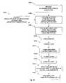
- FIG. 15is a diagram showing steps in a process for making a semiconductor assembly according to an embodiment of the invention as in FIG. 3 .
- FIG. 16is a diagrammatic sketch in a sectional view thru a stacked package assembly according to an embodiment of the invention, including a BGA stacked over an assembly according to an embodiment of the invention as shown in FIG. 4 .
- FIG. 17is a diagrammatic sketch in a sectional view thru a stacked package assembly according to an embodiment of the invention, including a flip chip die mounted over an assembly according to an embodiment of the invention as shown in FIG. 4 .
- FIG. 18is a diagrammatic sketch in a sectional view thru a stacked package assembly according to an embodiment of the invention, including passive devices mounted over an assembly according to an embodiment of the invention as shown in FIG. 4 .
- FIG. 19is a diagrammatic sketch in a sectional view thru a stacked package assembly according to an embodiment of the invention, including a SD QFP stacked over an assembly according to an embodiment of the invention as shown in FIG. 4 .
- FIG. 20is a diagrammatic sketch in a sectional view thru a stacked package assembly according to an embodiment of the invention, including a wire bonded die stacked over an assembly according to an embodiment of the invention as shown in FIG. 4 .
- FIG. 21is a diagrammatic sketch in a sectional view thru a stacked package assembly according to an embodiment of the invention, including a SD QFN/LFCSP stacked over an assembly according to an embodiment of the invention as shown in FIG. 4 .
- FIG. 22is a diagrammatic sketch in a sectional view thru a stacked package assembly according to an embodiment of the invention, including an optical sensor package stacked over an assembly according to an embodiment of the invention as shown in FIG. 4 .
- FIG. 23is a diagrammatic sketch in a sectional view thru a stacked package assembly according to an embodiment of the invention, including an optical sensor die mounted on an assembly according to an embodiment of the invention as shown in FIG. 4 .
- FIG. 24is a diagrammatic sketch in a sectional view thru a stacked package assembly according to another embodiment of the invention, including an optical sensor die mounted on an assembly according to an embodiment of the invention as shown in FIG. 4 .
- FIG. 25is a diagram showing steps in a process for making a stacked package assembly according to an embodiment of the invention as in FIG. 4 .
- FIG. 1there is shown in a diagrammatic sectional view generally at 1 an embodiment of a semiconductor assembly, including a first (“bottom”) package and a second (“top”) substrate stacked over the first package, in which the package and the second substrate are interconnected by wire bonding, according to an aspect of the invention.
- the bottom package 100is a conventional chip scale package (“CSP”).
- the bottom package 100includes a die 114 attached onto a bottom package substrate 112 having at least one metal layer (which may be referred to as an “interposer”).
- any of various substrate typesmay be used, including for example: a laminate with 2-6 metal layers, or a build up substrate with 4-8 metal layers, or a flexible polyimide tape with 1-2 metal layers, or a ceramic multilayer substrate.
- the bottom package substrate 112 shown by way of example in FIG. 1has two metal layers 121 , 123 , each patterned to provide appropriate circuitry and connected by way of vias 122 .
- the dieis conventionally attached to a surface of the substrate using an adhesive, typically referred to as the die attach epoxy, shown at 113 in FIG. 1 and, in the configuration in FIG.
- the side of the substrate onto which the die is attached(the “die attach” side) may be referred to as the “upper” side, and the metal layer on that side may be referred to as the “upper” metal layer, although the die attach side need not have any particular orientation in use.
- the dieis wire bonded onto wire bond sites on the upper metal layer of the substrate to establish electrical connections.
- the die 114 and the wire bonds 116are encapsulated, by matrix molding and saw singulation, with a molding compound 117 that provides protection from ambient and from mechanical stress to facilitate handling operations, and provides a first package upper surface 129 onto which the second substrate can be stacked.
- Bonding pads 119are provided on the lower metal layer 123 of the substrate 112 , for second level interconnection of the assembly to the underlying circuitry of, for example, a motherboard (not shown in the FIGs.).
- Solder masks 115 , 127are patterned over the metal layers 121 , 123 to expose the underlying metal at bonding sites for electrical connection, for example the wire bond sites and bonding pads for bonding the wire bonds 116 and solder balls 118 .
- the second (“top”) substrate 10having a first side and a second side, including a substrate dielectric 12 and at least one metal layer. Any of various substrate types may be used; the substrate 10 shown by way of example in FIG. 1 has two metal layers 21 , 23 , each patterned to provide appropriate circuitry and connected by way of vias 22 .
- the side of the second substrate that faces the first packageis the assembly is referred to as the first side, and the opposite side—the second side or “land” side—faces away from the first package in the assembly.
- solder masks 15 , 27are patterned over the metal layers 21 , 23 to expose the underlying metal at bonding sites for electrical connection, for example the wire bond sites for bonding the wire bonds 118 .
- the z-interconnect top substrate 10 and first package 100is made by way of wire bonds 118 connecting traces on the downward facing metal layer (the metal layer 21 ) of the top substrate with traces on the lower metal layer 123 of the first package substrate. At one end each wire bond 118 is electrically connected to downward facing surfaces of pads on the metal layer 21 of the top substrate 12 , and at the other end each wire bond is connected to lower surfaces of pads on the lower metal layer 123 of the first package substrate 112 .
- the wire bondsmay be formed by any wire bonding technique, well known in the art, such as is described, for example, in U.S. Pat. No. 5,226,582, which is hereby incorporated by reference herein.
- the package-to-package z-interconnect wire bondsare shown by way of example in FIG. 1 as having been made by forming a bead or bump on the surface of a pad on the lower metal layer of the top substrate, and then drawing the wire toward, and fusing it onto, a pad on the lower metal layer of the first package substrate.
- the wire bondscan be made in the inverse direction, that is, by forming a bead or bump on the lower surface of a pad on the lower metal layer of the first substrate, and then drawing the wire toward, and fusing it onto, a pad on the metal layer of the second substrate.
- wire bonding strategyfor the package-to-package z-interconnection will be determined according to the geometric arrangements of the margins of the stacked substrates and of the bonding surfaces on them. Also, as will be appreciated, in conventional wire bonding equipment the wire bond capillary strikes downward onto upwardly oriented bond pads and, accordingly, the assembly will be inverted according to the invention for the wire bonding procedure at least.
- the second (top) substrateis larger than the surface of the first package mold cap on which it is mounted, leaving an area at the periphery of the first side of the top package substrate on which the bond pads are exposed for the wire bonds 118 .
- the top substrateis (typically later) punch- or saw-singulated.
- the first packageis (in the example shown in FIG. 1 ) matrix molded and saw singulated (to provide vertical walls for the molding, as shown in FIG. 1 ), so that the die attach side of the bottom package substrate is covered by the molding.
- Bond pads in the upper metal layer at the die attach side of the bottom package substrateare connected to the die by wire bonds, and the upper metal layer is connected to the lower metal layer at the land side of the bottom package substrate through vias to the die attach side of the substrate, and the lower metal layer at the land side of the bottom package substrate is patterned to provide peripherally arranged bond pads for connection with the z-interconnection wires 118 .
- the structure according to the inventionallows for pre-testing of the CSP before assembly into the assembly, to permit rejection of nonconforming packages prior to assembly, and thereby to assure high final module test yields.
- the z-interconnect pads on the respective substratesare arranged on metal layers near the margins of the substrates.
- the location and order of the z-interconnect padsare generally arranged so that the z-interconnect pads on the top package substrate approximately overlie the corresponding z-interconnect pads on the bottom package when the packages are stacked.
- the second (top) substrate 10has a larger substrate footprint than that of the first (bottom) package 100 , to allow clearance for the wire bonds without electrical shorting to the edges of the metal layers of the substrates.
- an assembly encapsulation 107is formed, to enclose and protect the z-interconnect wire bonds and to provide mechanical integrity to the completed assembly.
- the assembly encapsulation 107covers the marginal area of the downward-facing first side of the second substrate, and encloses the z-interconnection wire bonds and wire loops and the vertical walls and edges of the bottom package, and covers the marginal area of the land side of the bottom package substrate including the wire loops and the wire bond pads to which the wire bonds are connected. This leaves an area of the land side of the bottom package substrate exposed for second-level interconnection.
- solder balls 318are reflowed onto bonding pads 119 on the lower metal layer of the substrate to provide interconnection to underlying circuitry of, for example, a motherboard (not shown in the FIGS.) of a final product, such as a computer.
- the assemblymay itself be saw-singulated; alternatively, the module may be individually molded rather than saw-singulated.
- the first packagemay have flip chip, rather than wire bonding, interconnection of the die to the first package substrate.
- the first packagemay be a stacked die package.
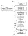
- FIG. 2shows, by way of example, a semiconductor assembly 2 generally as in FIG. 1 , except that in the example of FIG. 2 the bottom package is a stacked die package, having two wire bonded die.
- a bottom package 120is a conventional two-die stacked die CSP.
- a first dieis 114 attached using an adhesive to the (upward facing in the FIG.) die attach side of substrate 112 and a second die 144 is attached using an adhesive to the (upward facing) die attach side of the first die 114 .
- the first die 114 and the second die 144are electrically connected by wire bonds 116 , 146 , respectively, to bond sites in the upper metal layer 121 .
- the die 114 , 144 and the wire bonds 116 , 146are encapsulated, in this example by matrix molding and saw singulation, with a molding compound 217 , that provides protection from ambient and from mechanical stress to facilitate handling operations, and provides a bottom package upper surface 229 onto which a second substrate can be stacked.
- the second substrate 10is substantially the same as the second substrate 10 of FIG. 1 .
- the second substrate 10is affixed over first package 120 using an adhesive 103 between the mated upper surface 229 of the first package molding or mold caps, and the downward facing surface 19 of the second substrate.
- the z-interconnection wire bonds 218are formed. Once the z-interconnect wire bonds have been formed connecting the stacked first and second packages, an assembly encapsulation 207 is formed, to enclose and protect the z-interconnect wire bonds and to provide mechanical integrity to the completed assembly.
- the assembly encapsulation 207covers the marginal area of the downward-facing first side of the second substrate, and encloses the z-interconnection wire bonds and wire loops and the vertical walls and edges of the bottom package, and covers the marginal area of the land side of the bottom package substrate including the wire loops and the wire bond pads to which the wire bonds are connected. This leaves an area of the land side of the bottom package substrate exposed for second-level interconnection. Solder balls are reflowed onto bonding pads 119 on the lower metal layer of the exposed lower package substrate to provide interconnection to underlying circuitry of, for example, a motherboard (not shown in the FIGS.) of a final product, such as a computer, as shown by way of example in FIG. 3 .
- the exposed side of the second substrateprovides for second-level interconnection.
- the embodiment shown in FIG. 4has second level interconnect solder balls 418 mounted onto pads 419 on the metal layer 23 , for connection of the assembly to underlying circuitry such as a motherboard.
- the exposed portion of the first package substrateis available for stacking additional components such as packages, die, or passive devices.
- the exposed portion of the first package substratehas a more limited area than the second package substrate, limiting the number of interconnections that can be made at the first package side.
- the part of the assembly molding 207 that covers the marginal area of the land side of the land side of the first package substratemust be thick enough to accommodate the loop height of the wire bonds 118 (plus a tolerance).
- the thickness of the molding at the wire loopsis in the range about 50 um to about 200 um.
- the wire loop height in practicemay be as little as about 35 um and, accordingly, a molding thickness over the marginal area of as little as about 100 um can be achieved in such embodiments.
- a greater mold heightwill be required where forward wire bonding is employed, as the wire loop height over a ball (or bump) as more usually about 100 um or greater using currently available wire bonding techniques forming wire having about 1 mil thickness.
- Embodiments as shown for example in FIG. 3in which the second level interconnection is made at the exposed region of the land side of the first package substrate, permit stacking of much larger additional components over the assembly, as shown in FIGS. 7B and 8B , for example.
- Embodiments as shown for example in FIG. 4in which the second level interconnection is made at the land side of the second package substrate, are shown in FIGS. 16 and 17 , for example.
- one or more additional componentscan be mounted upon and electrically connected with, the land side of the first package substrate within the cavity in the encapsulation.
- FIGS. 5A and 5Bare diagrammatic sketches in plan view showing the land side and the die attach side, respectively, of a suitable first package substrate as illustrated at 112 in FIG. 1 .
- the solder maskwhich obscures the patterned metal layer beneath except where sites on the metal layer are revealed by openings in the solder mask. Openings in the solder mask reveal sites in the patterned metal layer at the land side of the substrate, including ball pads (e.g., 53 ) arrayed in a middle region of the substrate surface, and bond fingers (e.g., 56 ), arranged in a marginal area near the edge 52 of the substrate.
- tracese.g., 523
- the metal layerwhich variously connect the ball pads 53 and the bond fingers 56 , and/or connect ball pads 53 with vias (e.g., 522 ) which electrically connect traces in the patterned metal layer at the land side of the substrate with traces in the patterned metal layer at the die attach side of the substrate.
- the assembly encapsulationcovers the bond pads 56 and the wire loops formed at the pads 56 ; the encapsulation is limited at the land side of the substrate to a marginal area, indicated in FIG. 5A by the broken line 58 , so the region of the land side of the first package substrate bounded by the marginal encapsulation, that is, within the broken line 58 , is left exposed following formation of the assembly molding. Accordingly, the ball pads 53 are available for attachment of additional devices (as illustrated for example in FIG. 4 ) or, more preferably, for z-level interconnection of the assembly to underlying circuitry (as illustrated for example in FIG. 3 ).
- the ball pads 53are additionally available as test probe sites for testing the package prior to assembly, or for testing the package assembly, if desired, prior to mounting the second level interconnect solder balls.
- the encapsulated marginal areahas a width (MW in FIG. 5A ) determined by the sum of the lengths of the bond fingers, the length of the trace to the bond finger, and the width of the saw street. Additionally, some mold flash may appear on the substrate surface at the inner edge of the margin (at the broken line 58 in FIG. 5A ). Where the substrate is provided as one in a strip or array, some substrate material at the edge is lost to the saw width during saw singulation of the first package.
- the bond finger lengthis about 250 um
- the finger trace lengthis about 50 um
- an allowance for mold resin bleedcan be about 500 um.
- the sawtypically consumes about 50 um.
- the number and arrangement of the ball pads 53depend upon the nominal ball diameter, as the balls must not contact each other, or be too close together, when collapsed. Also as a practical matter the size and proximity of the ball pads 53 are limited by limits of resolution in fabricating the traces and, particularly, the solder mask openings.
- the ball padsare generally circular with a diameter about 280 um, and are arranged in a square or rectangular array at a center-to-center distance about 500 um. (The distance between nearest edges of adjacent solder mask openings is typically not less than about 0.20 times the center-to-center distance.)
- the die attach side of the first package substrate, with die attached,is illustrated in FIG. 5B .
- the die 114is affixed, active side upward, onto the die attach side of the substrate.
- the diehas four edges defining a square.
- Wire bond pads 51are arranged in rows near the four edges of the die.
- As on the land side of the substrate, most of the surface of the die attach sideis covered by a solder mask, except where sites on the metal layer are revealed by openings in the solder mask, including particularly rows (one row along each edge of the die, in this example) of bond fingers (e.g., 54 ).
- Wires 116connect the die pads 51 with the bond fingers 54 .
- the solder maskObscured by the solder mask are traces (e.g., 521 ) in the metal layer connecting bond fingers 54 to vias (e.g., 522 ) which electrically connect traces in the patterned metal layer at the die attach side of the substrate with traces in the patterned metal layer at the land side.
- the first package dieis connected by way of the wires to traces in the metal layer on the die attach side of the first package substrate, and by way of vias to traces and to z-interconnect wire bond fingers in the metal layer on the land side.
- the z-interconnect wiresconnect the bond fingers on the land side of the first package substrate to bond fingers on the die attach side of the second package substrate.
- FIGS. 6A and 6Bare diagrammatic sketches in plan view showing the second side and the first side, respectively, of a suitable second substrate as illustrated at 10 in FIG. 1 .
- the solder maskmost of the surface of the land side is covered by the solder mask, which obscures the patterned metal layer beneath except where sites on the metal layer are revealed by openings in the solder mask. Openings in the solder mask reveal sites in the patterned metal layer at the land side of the substrate, including ball pads (e.g., 63 ) arrayed in a middle region of the substrate surface.
- tracese.g., 623
- viase.g., 622
- the view of the second substrate in FIG. 6Ais substantially a view of a surface of the assembly.
- the ball pads 63are available for z-level interconnection of the assembly to underlying circuitry (as illustrated for example in FIG. 4 ) or, more preferably, for attachment of additional devices (as illustrated for example in FIG. 3 ).
- the ball pads 63are additionally available as test probe sites for testing the package prior to assembly, and for testing the package assembly, if desired, prior to mounting the second level interconnect solder balls.
- the ball attach pads on the land side of the second substratemay be employed to facilitate testing of the assembly using a conventional test socket.
- Such testing of the assemblycan be carried out, for example, following attachment of the second substrate as a top substrate, but prior to formation of the overall assembly molding, or prior to z-interconnect wire-bonding. Testing, facilitated according to the constructs of the invention, at any of various stages in manufacture, can significantly reduce the likelihood of further processing of components that do not meet specifications.
- the die attach side of the second substrateis illustrated in FIG. 6B .
- a solder maskAs on the land side of the second substrate, most of the surface of the first side is covered by a solder mask, except where sites on the metal layer are revealed by openings in the solder mask, including particularly z-interconnect bond fingers (e.g., 66 ) arranged in a marginal area near the edge 62 of the substrate.
- Obscured by the solder maskare traces (e.g., 621 ) in the metal layer connecting vias (e.g., 622 ) which electrically connect traces in the patterned metal layer at the first side of the substrate with traces in the patterned metal layer at the land side, to z-interconnect bond fingers 66 .
- the second substrate z-interconnect pads (bond fingers) 66are formed by patterning regions of the metal layer situated at the margin on the first side of the second package substrate 12 .
- the marginextends beyond the footprint of the stacked first package substrate 112 , which for a matrix molded and saw-singulated CSP first package is substantially the same as the CSP package molding 217 ; this footprint is indicated by the broken line 68 in FIG. 6B .
- the width of the margincan be less about 1 mm, and, in order to provide adequate clearance for the wire bonding the width of the margin may preferably be greater than about 0.2 mm. Nominally in some embodiments the margin is about 0.5 mm.
- z-interconnect the bond fingers at the first side of the second substrateare connected by traces in the metal layer on first side of the first package substrate by way of vias to traces and to z-interconnect wire bond fingers in the metal layer on the land side, where interconnection of the assembly is made to additional devices stacked over the assembly or to an underlying substrate (second level interconnection).
- the z-interconnect wiresconnect the bond fingers on the first side of the second package substrate to bond fingers on the land side of the first package substrate, and the first package die are interconnected as appropriate by way of the traces, wires, and vias to the pads on the land sides of the first package substrate, where interconnection of the assembly is made to an underlying substrate (second level interconnection) or to additional devices stacked over the assembly.
- the die in the first packageare interconnected as desired to exposed pads on the land sides of the first package substrate and the second substrate at the top and bottom of the completed assembly.
- the second substratenecessarily has a larger footprint than the first package substrate, to accommodate the z-interconnection between the package substrates.
- z-interconnectsare arranged along all four edges of the packages and, accordingly, the second package is both wider and longer than the first package.
- z-interconnectionmay be made between bond fingers on fewer than all four edges, as for example along only one edge, or along two opposite edges. In such embodiments (unless a larger die in the second substrate requires a larger footprint), the second package need be larger (longer or wider) than the first package only in one direction.
- the first packagemay have any of a variety of functionalities.
- the CSP packagecan be a DSP, ASIC, GPU; or, the CSP package can be a memory, such as Flash, DRAM, SRAM.
- the processor chip in a flip chip bottom packagecan be, for example, an ASIC, or a GPU, or a CPU, often an ASIC.
- the bottom packageis a memory package it can be a stacked die memory package.
- a shielded flip chip die-up bottom packagecan be particularly suitable for higher speed applications, particularly for RF frequency processing, as in mobile communications applications.
- an additional packageis attached to the assembly on an available (exposed) substrate surface, and preferably on the exposed land side of the second package substrate.
- the additional packageis attached to the assembly on the exposed land side of the second substrate.
- the assembly as shown for example in FIG. 1 or 2can provide a useful platform upon which to stack components having additional functionalities, as shown for example in FIGS. 7A through 13 .
- the second package substrateis fully exposed, it can accommodate any of a variety of component (die or package) configurations and sizes, and all that is required for compatibility of the assembly with the components is that the traces on the exposed second package substrate be suitably routed to accept the additional component.
- a ball grid array (BGA) packagecan be mounted over an assembly constructed as described above with reference to FIG. 3 .
- a BGA package 710 having interconnect solder balls 718is aligned with and mounted upon the land side of a second package 10 substrate, and the solder balls are reflowed onto ball pads in the metal layer 23 to form a module 70 .
- the BGA footprintis smaller than that of the assembly; in the module 72 shown in FIG. 7B , the footprint of the BGA 720 is larger than that of the assembly, and the ball array has more interconnect solder balls, which accordingly occupy more ball pads on the second package 10 substrate.
- the BGAis a stacked die package
- FIG. 7Athe BGA is a single die package.
- an additional land grid array (LGA) packagecan be mounted over an assembly constructed as described above with reference to FIG. 3 .
- a LGA package 810 having land interconnects 818is aligned with and mounted upon the land side of a second package 10 substrate, and the land interconnects are reflowed onto pads in the metal layer 23 to form a module 80 .
- the LGA footprintis smaller than that of the assembly; in the module 82 shown in FIG. 8B , the footprint of the LGA 820 is larger than that of the assembly, and the array has more land interconnects, which accordingly occupy more pads on the second package 10 substrate.
- the LGAis a stacked die package
- FIG. 8Athe LGA is a single die package.
- a configuration having a larger additional package mounted over the stacked package assembly as shown in FIGS. 7A and 8Amay, for example, include processors in the first package 10 , and a memory package as the additional package 720 or 820 .
- the minimum sizes of footprints of the CSP 100 and of the second substrate 10 in the assemblyare determined principally by the dimensions of the die in the first package, and this generally relates to the functionality of the die.
- ASICsmay be comparatively very small, for example, and different processors may be of significantly different sizes.
- Memory dieon the other hand, may be comparatively large.
- a digital signal processor (DSP) packagefor example, has a footprint typically in the range 12 ⁇ 12 mm to 16 ⁇ 16 mm.
- a memory packagetypically has a footprint in the range 8 ⁇ 10 mm to 18 ⁇ 18 mm. Accordingly, if the assembly as in FIG. 3 includes a DSP in the first package 10 of the assembly, establishing a footprint of 16 ⁇ 16 mm for the assembly 3 , the manufacturer may according to the specifications of the customer select either a smaller LGA memory package (e.g. 810 in FIG. 8A , giving a module 80 ) or a larger LGA memory package (e.g. 820 in FIG. 8B , giving a module 82 ). Thus, for embodiments as in FIGS. 7A , 7 B, 8 A, 8 B, the manufacturer can mix-and-match assembly platforms with selected memory BGAs or LGAs according to function (memory capacity and speed; memory type) and according to costs from various suppliers.
- functionmemory capacity and speed; memory type
- FIG. 9shows a module 90 having a stacked die quad flat package 900 , accompanied by passive devices 96 , mounted over a semiconductor assembly constructed generally as in FIG. 3 .
- FIG. 10shows a module 100 having a stacked die quad flat nonleaded lead frame chip scale package 1000 , accompanied by passive devices 106 , mounted over a semiconductor assembly constructed generally as in FIG. 3 .
- FIG. 11shows a module 110 having a wire bonded die 1100 , accompanied by passive devices 1106 , mounted over a semiconductor assembly constructed generally as in FIG.
- FIG. 12shows a module 120 having a flip chip mounted die 1200 , accompanied by passive devices 1206 , mounted over a semiconductor assembly constructed generally as in FIG. 3 ; an underfill protects the flip chip interconnects.
- FIG. 13shows a module 130 having an optical sensor package 1300 , which may be an image forming device, accompanied by passive devices 1306 , mounted over a semiconductor assembly constructed generally as in FIG. 3 ; light passes through a transparent cover or lens as indicated by arrows 1320 to reach the active side of the wire-bonded light sensor die.
- FIG. 14shows an assembly 140 , including a semiconductor assembly generally as shown in FIG. 3 , having a heat spreader 1400 mounted upon the land side of the second package substrate.
- the additional packageis attached to the assembly on the exposed area of the land side of the first package substrate, in the cavity in the assembly encapsulation.
- the assembly of FIG. 1 or 2with second level interconnection on the land side of second substrate, as shown in FIG. 4 , can provide a useful platform upon which to stack components having additional functionalities, as shown for example in FIGS. 16 through 24 .
- the traces on the first package substratemust suitably routed to accept the additional component.
- a ball grid array (BGA) packagecan be mounted over an assembly constructed as described above with reference to FIG. 4 .
- BGAball grid array
- a BGA package 710 having interconnect solder balls 718is aligned with and mounted upon the exposed area of the land side of a first package 100 substrate, and the solder balls are reflowed onto ball pads in the metal layer 123 to form a module 160 .
- an additional diecan be mounted and electrically connected in a flip chip manner over an assembly constructed as described above with reference to FIG. 4 .
- a flip chip 1200is aligned with and mounted in the cavity upon the exposed area of the land side of a first package 100 substrate and connected to pads 123 to form a module 170 .
- additional passive devicescan be mounted and electrically connected over an assembly constructed as described above with reference to FIG. 4 .
- passive devices 182are mounted in the cavity upon the exposed area of the land side of a first package 100 substrate and connected to pads 123 to form a module 170 .
- a stacked die quad flat packagecan be mounted and electrically connected over an assembly constructed as described above with reference to FIG. 4 .
- FIG. 19a stacked die quad flat package
- stacked die quad flat package 900is mounted in the cavity upon the exposed area of the land side of a first package 100 substrate and connected to pads 123 to form a module 180 .
- an additional diecan be mounted and electrically connected by wire bonding over an assembly constructed as described above with reference to FIG. 4 .
- a die 1100is mounted active side upward in the cavity upon the exposed area of the land side of a first package 100 substrate and connected by wire bonds to pads 123 to form a module 200 .
- a stacked die quad flat nonleaded lead frame chip scale package 1000is mounted over a stacked package assembly constructed generally as in FIG. 4 .
- stacked die quad flat nonleaded lead frame CSP 1000is mounted in the cavity upon the exposed area of the land side of a first package 100 substrate and connected to pads 123 to form a module 210 .
- an optical sensor package 1300which may be an image forming device, is mounted over a stacked package assembly constructed generally as in FIG. 4 .
- optical sensor package 1300is mounted in the cavity upon the exposed area of the land side of a first package 100 substrate and connected to pads 123 to form a module 220 .
- Lightpasses through a transparent cover or lens 1302 as indicated by arrows 1320 to reach the active side of the wire-bonded light sensor die.
- an optical sensor diewhich may be an image forming device, is mounted over a stacked package assembly constructed generally as in FIG. 4 .
- the dieis connected by wire bonds to pads 123 to form a module 230 .
- a transparent cover or lens 1402is supported by a frame 1404 mounted upon the assembly encapsulation 107 . Light passes through the transparent cover or lens 1402 as indicated by arrows 1420 to reach the active side of the wire-bonded light sensor die.
- the cavity assembly encapsulation 247is configured and dimensioned to accommodate the thickness of an optical sensor die mounted onto and electrically connected with the stacked package assembly as in FIG. 23 , and a transparent cover or lens 2402 is supported by a perimeter seal 2404 mounted within a recess in the assembly encapsulation 247 .
- the inventionfeatures an assembly having a first (CSP) package and a second substrate stacked over the CSP package, and having wire bonding z-interconnect between the first package substrate and the second substrate, in which the assembly is encapsulated in such a way that the land side of the second substrate is exposed and a portion of the land side of the first (CSP) package is exposed.
- the assemblyconstitutes a platform for combination with any of a variety of additional components. Accordingly, in various configurations second level interconnection of the assembly is made at the land side of one of the substrates (preferably the first package substrate), and one or more additional, components are stacked over the land side of the other substrate (preferably the second substrate).
- the additional componentsmay be selected by the manufacturer on the product assembly floor, and may be selected from among off-the-shelf components.
- the semiconductor assembly of the inventioncan be employed in any of a diverse variety of applications, such as, for example, computers, portable communications devices, consumer products.
- the semiconductor assembly according to the inventioncan be used for building computers, and, for example, in telecommunications, consumer and industrial electronics devices.
- the inventionprovides for assembly of more than one semiconductor in a thin and minimal footprint package at high final test yields. Construction of the individual packages allows testing before they are assembled into the assembly, assuring that only acceptably good package components are employed in assembly and, accordingly, ensuring high assembly yields.
- the inventionprovides for flexibility in design, particularly in selection of components having selected functionalities, and enables the use of standard packages, reducing the need for custom design and reducing cost.
- the processincludes steps of providing a second substrate, preferably as a strip or matrix of substrates, providing a CSP (such as a matrix molded and saw singulated CSP) including a CSP package substrate and at least one die, inverting the CSP package in relation to the LGA package, applying adhesive onto a surface of the molding of the CSP package, inverting the CSP and placing the inverted CSP upon the second substrate so that the adhesive contracts a surface of the substrate, curing the adhesive, and forming z-interconnects between the CSP substrate and the second substrate.
- a CSPsuch as a matrix molded and saw singulated CSP
- the packagecan be tested prior to assembly, and packages not meeting requirements for performance or reliability can be discarded, so that first packages tested as “good” are used in the assembled module.
- Testing of CSPsis well established in the industry, and typically is done by accessing contact to the solder ball pads.
- the completed assemblycan be tested in the same manner as for testing BGAs.
- FIG. 15is a flow diagram showing a process for assembly of a stacked package assembly as shown for example in FIG. 3 .
- a step 1502an unsingulated strip of substrates is provided.
- singulated chip scale packagesare provided.
- the singulated CSP packagesare protected by a molding, and preferably are tested (*) and identified as “good”.
- adhesiveis dispensed over the upper surface of the molding on “good” singulated CSP packages.
- a pick-and-place operationis carried out to invert and place “good” CSP packages on the substrates in the strip; the adhesive is then situated between the surface of the first package molding and the first surface of the substrate.
- a step 1510the adhesive is cured.
- a plasma clean operationis performed in preparation for a step 1514 in which wire bond z-interconnections are formed between wire bond sites on the land side of the CSP and the first side of the second substrate.
- an additional plasma cleanmay be performed, followed by the formation of the stacked package assembly molding in a step 1518 .
- the molding apparatusis configured to allow molding compound to encapsulate the z-interconnection wire loops, and to prevent incursion of molding compound into an inner area of the land side of the CSP.
- the second-level interconnect solder ballsare attached to the exposed inner area of the land side of the CSP.
- the completed assembliesare tested (*) and singulated from the strip by saw singulation, and packaged for further use.
- FIG. 25is a flow diagram showing a process for assembly of a stacked package assembly as shown for example in FIG. 4 .
- a step 2502an unsingulated strip of substrates is provided.
- singulated chip scale packagesare provided.
- the singulated CSP packagesare protected by a molding, and preferably are tested (*) and identified as “good”.
- adhesiveis dispensed over the molding on the CSPs.
- a step 2508a pick-and-place operation is carried out to invert and place “good” CSP packages on the substrates.
- the adhesiveis cured.
- a plasma clean operationis performed in preparation for a step 2514 in which wire bond z-interconnections are formed between wire bond sites on the land sides of the CSP and the LGA substrate.
- an additional plasma cleanmay be performed, followed by the formation of the stacked package assembly molding in a step 2518 .
- the molding apparatusis configured to allow molding compound to encapsulate the z-interconnection wire loops, and to prevent incursion of molding compound into an inner area of the land side of the CSP.
- the second-level interconnect solder ballsare attached to the exposed land side of the substrate.
- the completed assembliesare tested (*) and singulated from the strip by saw singulation, and packaged for further use.
Landscapes
- Engineering & Computer Science (AREA)
- Microelectronics & Electronic Packaging (AREA)
- Power Engineering (AREA)
- Physics & Mathematics (AREA)
- Condensed Matter Physics & Semiconductors (AREA)
- General Physics & Mathematics (AREA)
- Computer Hardware Design (AREA)
- Manufacturing & Machinery (AREA)
- Wire Bonding (AREA)
- Encapsulation Of And Coatings For Semiconductor Or Solid State Devices (AREA)
- Structures Or Materials For Encapsulating Or Coating Semiconductor Devices Or Solid State Devices (AREA)
Abstract
Description
Claims (17)
Priority Applications (1)
| Application Number | Priority Date | Filing Date | Title |
|---|---|---|---|
| US11/397,027US7429787B2 (en) | 2005-03-31 | 2006-03-31 | Semiconductor assembly including chip scale package and second substrate with exposed surfaces on upper and lower sides |
Applications Claiming Priority (4)
| Application Number | Priority Date | Filing Date | Title |
|---|---|---|---|
| US66727705P | 2005-03-31 | 2005-03-31 | |
| US69218305P | 2005-06-20 | 2005-06-20 | |
| US11/306,628US7364945B2 (en) | 2005-03-31 | 2006-01-04 | Method of mounting an integrated circuit package in an encapsulant cavity |
| US11/397,027US7429787B2 (en) | 2005-03-31 | 2006-03-31 | Semiconductor assembly including chip scale package and second substrate with exposed surfaces on upper and lower sides |
Related Parent Applications (1)
| Application Number | Title | Priority Date | Filing Date |
|---|---|---|---|
| US11/306,628Continuation-In-PartUS7364945B2 (en) | 2005-03-31 | 2006-01-04 | Method of mounting an integrated circuit package in an encapsulant cavity |
Publications (2)
| Publication Number | Publication Date |
|---|---|
| US20060220210A1 US20060220210A1 (en) | 2006-10-05 |
| US7429787B2true US7429787B2 (en) | 2008-09-30 |
Family
ID=37069349
Family Applications (1)
| Application Number | Title | Priority Date | Filing Date |
|---|---|---|---|
| US11/397,027Active2026-01-27US7429787B2 (en) | 2005-03-31 | 2006-03-31 | Semiconductor assembly including chip scale package and second substrate with exposed surfaces on upper and lower sides |
Country Status (5)
| Country | Link |
|---|---|
| US (1) | US7429787B2 (en) |
| JP (1) | JP5346578B2 (en) |
| KR (1) | KR101213661B1 (en) |
| TW (1) | TWI442520B (en) |
| WO (1) | WO2006118720A2 (en) |
Cited By (45)
| Publication number | Priority date | Publication date | Assignee | Title |
|---|---|---|---|---|
| US20070178667A1 (en)* | 2006-01-31 | 2007-08-02 | Stats Chippac Ltd. | Wafer level chip scale package system |
| US20070210443A1 (en)* | 2006-03-08 | 2007-09-13 | Stats Chippac Ltd. | Integrated circuit package on package system |
| US20070210424A1 (en)* | 2006-03-08 | 2007-09-13 | Stats Chippac Ltd. | Integrated circuit package in package system |
| US20080211084A1 (en)* | 2007-03-03 | 2008-09-04 | Seng Guan Chow | Integrated circuit package system with interposer |
| US20080230887A1 (en)* | 2007-03-23 | 2008-09-25 | Advanced Semiconductor Engineering, Inc. | Semiconductor package and the method of making the same |
| US20080318348A1 (en)* | 2007-06-25 | 2008-12-25 | Spansion Llc | Method of constructing a stacked-die semiconductor structure |
| US20090095510A1 (en)* | 2007-10-10 | 2009-04-16 | Epson Toyocom Corporation | Electronic device, electronic module, and methods for manufacturing the same |
| US20090127689A1 (en)* | 2005-08-26 | 2009-05-21 | Micron Technology, Inc. | Microelectronic device packages, stacked microelectronic device packages, and methods for manufacturing microelectronic devices |
| US20090236735A1 (en)* | 2008-03-19 | 2009-09-24 | Micron Technology, Inc. | Upgradeable and repairable semiconductor packages and methods |
| US20090243072A1 (en)* | 2008-02-29 | 2009-10-01 | Jong-Woo Ha | Stacked integrated circuit package system |
| US20090256249A1 (en)* | 2006-06-29 | 2009-10-15 | Cheemen Yu | Stacked, interconnected semiconductor package |
| US20090294941A1 (en)* | 2008-05-30 | 2009-12-03 | Oh Jihoon | Package-on-package system with heat spreader |
| US20100000775A1 (en)* | 2008-07-03 | 2010-01-07 | Advanced Semiconductor Engineering, Inc. | Circuit substrate and method of fabricating the same and chip package structure |
| US20100055836A1 (en)* | 2006-06-29 | 2010-03-04 | Cheeman Yu | Method of stacking and interconnecting semiconductor packages via electrical connectors extending between adjoining semiconductor packages |
| US20100140761A1 (en)* | 2006-08-08 | 2010-06-10 | Stats Chippac, Ltd. | Quad Flat Package |
| US20100171206A1 (en)* | 2009-01-07 | 2010-07-08 | Chi-Chih Chu | Package-on-Package Device, Semiconductor Package, and Method for Manufacturing The Same |
| US20100171207A1 (en)* | 2009-01-07 | 2010-07-08 | Chi-Chih Shen | Stackable semiconductor device packages |
| US20100171205A1 (en)* | 2009-01-07 | 2010-07-08 | Kuang-Hsiung Chen | Stackable Semiconductor Device Packages |
| US20100224979A1 (en)* | 2008-03-27 | 2010-09-09 | Flynn Carson | Stacked integrated circuit package system and method for manufacturing thereof |
| US20110049704A1 (en)* | 2009-08-31 | 2011-03-03 | Advanced Semiconductor Engineering, Inc. | Semiconductor device packages with integrated heatsinks |
| US20110117700A1 (en)* | 2009-11-18 | 2011-05-19 | Advanced Semiconductor Engineering, Inc. | Stackable semiconductor device packages |
| US20110193205A1 (en)* | 2010-02-10 | 2011-08-11 | Advanced Semiconductor Engineering, Inc. | Semiconductor device packages having stacking functionality and including interposer |
| US20110233748A1 (en)* | 2010-03-24 | 2011-09-29 | Mukul Joshi | Integrated circuit packaging system with interconnect and method of manufacture thereof |
| US20120104517A1 (en)* | 2010-11-01 | 2012-05-03 | Siliconware Precision Industries Co., Ltd. | Package structure with micro-electromechanical element and manufacturing method thereof |
| US20120205795A1 (en)* | 2011-02-15 | 2012-08-16 | Samsung Electronics Co., Ltd. | Stacked package and method of manufacturing the same |
| US20120235307A1 (en)* | 2011-03-15 | 2012-09-20 | Jong-Woo Ha | Integrated circuit packaging system with lead frame stacking module and method of manufacture thereof |
| US8278746B2 (en) | 2010-04-02 | 2012-10-02 | Advanced Semiconductor Engineering, Inc. | Semiconductor device packages including connecting elements |
| US8405212B2 (en) | 2009-12-31 | 2013-03-26 | Advanced Semiconductor Engineering, Inc. | Semiconductor package |
| US8507318B2 (en) | 2005-08-19 | 2013-08-13 | Micron Technology, Inc. | Method for manufacturing microelectronic devices |
| US20130241044A1 (en)* | 2012-03-16 | 2013-09-19 | Samsung Electronics Co., Ltd. | Semiconductor package having protective layer and method of forming the same |
| US8569885B2 (en) | 2010-10-29 | 2013-10-29 | Advanced Semiconductor Engineering, Inc. | Stacked semiconductor packages and related methods |
| US8624374B2 (en) | 2010-04-02 | 2014-01-07 | Advanced Semiconductor Engineering, Inc. | Semiconductor device packages with fan-out and with connecting elements for stacking and manufacturing methods thereof |
| US8643167B2 (en) | 2011-01-06 | 2014-02-04 | Advanced Semiconductor Engineering, Inc. | Semiconductor package with through silicon vias and method for making the same |
| US8765525B2 (en) | 2011-06-16 | 2014-07-01 | Stats Chippac Ltd. | Method of manufacturing an integrated circuit packaging system including lasering through encapsulant over interposer |
| US9029962B1 (en)* | 2011-10-12 | 2015-05-12 | Amkor Technology, Inc. | Molded cavity substrate MEMS package fabrication method and structure |
| US20150221570A1 (en)* | 2014-02-04 | 2015-08-06 | Amkor Technology, Inc. | Thin sandwich embedded package |
| US9171792B2 (en) | 2011-02-28 | 2015-10-27 | Advanced Semiconductor Engineering, Inc. | Semiconductor device packages having a side-by-side device arrangement and stacking functionality |
| US9196597B2 (en) | 2010-01-13 | 2015-11-24 | Advanced Semiconductor Engineering, Inc. | Semiconductor package with single sided substrate design and manufacturing methods thereof |
| US9349611B2 (en) | 2010-03-22 | 2016-05-24 | Advanced Semiconductor Engineering, Inc. | Stackable semiconductor package and manufacturing method thereof |
| US9365415B2 (en) | 2014-01-02 | 2016-06-14 | STMicroelectronics (Shenzhen) R&D Co. Ltd | Compact electronic package with MEMS IC and related methods |
| US9466545B1 (en)* | 2007-02-21 | 2016-10-11 | Amkor Technology, Inc. | Semiconductor package in package |
| US10008533B2 (en) | 2015-12-01 | 2018-06-26 | Samsung Electronics Co., Ltd. | Semiconductor package |
| US20190237436A1 (en)* | 2007-04-12 | 2019-08-01 | Micron Technology, Inc. | System in package (sip) with dual laminate interposers |
| US20200118991A1 (en)* | 2018-10-15 | 2020-04-16 | Intel Corporation | Pre-patterned fine-pitch bond pad interposer |
| US20230268319A1 (en)* | 2021-10-14 | 2023-08-24 | Advanced Micro Devices, Inc. | Stacking semiconductor devices by bonding front surfaces of different dies to each other |
Families Citing this family (48)
| Publication number | Priority date | Publication date | Assignee | Title |
|---|---|---|---|---|
| AU2003298595A1 (en)* | 2002-10-08 | 2004-05-04 | Chippac, Inc. | Semiconductor stacked multi-package module having inverted second package |
| US7394148B2 (en) | 2005-06-20 | 2008-07-01 | Stats Chippac Ltd. | Module having stacked chip scale semiconductor packages |
| US8796836B2 (en) | 2005-08-25 | 2014-08-05 | Micron Technology, Inc. | Land grid array semiconductor device packages |
| US8120156B2 (en)* | 2006-02-17 | 2012-02-21 | Stats Chippac Ltd. | Integrated circuit package system with die on base package |
| KR100813621B1 (en)* | 2006-10-03 | 2008-03-17 | 삼성전자주식회사 | Stacked Semiconductor Device Package |
| TWI321838B (en)* | 2006-11-08 | 2010-03-11 | Advanced Semiconductor Eng | Stacked type chip package, chip package and process thereof |
| KR100817091B1 (en)* | 2007-03-02 | 2008-03-26 | 삼성전자주식회사 | Multilayer semiconductor package and manufacturing method thereof |
| US7868441B2 (en)* | 2007-04-13 | 2011-01-11 | Maxim Integrated Products, Inc. | Package on-package secure module having BGA mesh cap |
| US8409920B2 (en)* | 2007-04-23 | 2013-04-02 | Stats Chippac Ltd. | Integrated circuit package system for package stacking and method of manufacture therefor |
| US7777354B2 (en)* | 2007-06-05 | 2010-08-17 | Stats Chippac Ltd. | Integrated circuit package system with leaded package |
| SG148901A1 (en)* | 2007-07-09 | 2009-01-29 | Micron Technology Inc | Packaged semiconductor assemblies and methods for manufacturing such assemblies |
| US7772696B2 (en)* | 2007-08-30 | 2010-08-10 | Nvidia Corporation | IC package having IC-to-PCB interconnects on the top and bottom of the package substrate |
| US8106505B2 (en)* | 2007-10-31 | 2012-01-31 | International Business Machines Corporation | Assembly including plural through wafer vias, method of cooling the assembly and method of fabricating the assembly |
| US8536692B2 (en)* | 2007-12-12 | 2013-09-17 | Stats Chippac Ltd. | Mountable integrated circuit package system with mountable integrated circuit die |
| US8247894B2 (en)* | 2008-03-24 | 2012-08-21 | Stats Chippac Ltd. | Integrated circuit package system with step mold recess |
| SG142321A1 (en) | 2008-04-24 | 2009-11-26 | Micron Technology Inc | Pre-encapsulated cavity interposer |
| US8270176B2 (en)* | 2008-08-08 | 2012-09-18 | Stats Chippac Ltd. | Exposed interconnect for a package on package system |
| KR101711045B1 (en) | 2010-12-02 | 2017-03-02 | 삼성전자 주식회사 | Stacked Package Structure |
| DE102010062559A1 (en) | 2010-12-07 | 2012-06-14 | Robert Bosch Gmbh | Microelectromechanical sensor module and corresponding manufacturing method |
| KR20120131530A (en) | 2011-05-25 | 2012-12-05 | 삼성전자주식회사 | Memory device and and fabricating method thereof |
| KR101274460B1 (en)* | 2011-11-22 | 2013-06-18 | 삼성전기주식회사 | Semiconductor package and manufacturing method threrof |
| KR101896665B1 (en)* | 2012-01-11 | 2018-09-07 | 삼성전자주식회사 | Semiconductor package |
| US9035421B2 (en) | 2013-03-01 | 2015-05-19 | Qualcomm Incorporated | High quality factor inductor implemented in wafer level packaging (WLP) |
| US9373583B2 (en) | 2013-03-01 | 2016-06-21 | Qualcomm Incorporated | High quality factor filter implemented in wafer level packaging (WLP) integrated device |
| KR101994715B1 (en)* | 2013-06-24 | 2019-07-01 | 삼성전기주식회사 | Manufacturing method of electronic component module |
| KR101548799B1 (en) | 2013-06-24 | 2015-08-31 | 삼성전기주식회사 | Electric component module and manufacturing method threrof |
| CN103489792B (en)* | 2013-08-06 | 2016-02-03 | 江苏长电科技股份有限公司 | First be honored as a queen and lose three-dimensional systematic flip chip encapsulation structure and process |
| CN103390563B (en)* | 2013-08-06 | 2016-03-30 | 江苏长电科技股份有限公司 | Erosion flip-chip of being first honored as a queen three-dimensional systematic metal circuit board structure &processes method |
| US20150048463A1 (en)* | 2013-08-16 | 2015-02-19 | Txc Corporation | Package device for microelectromechanical inertial sensor |
| KR102171020B1 (en) | 2013-10-16 | 2020-10-29 | 삼성전자주식회사 | X-ray system, semiconductor package, and tray having X-ray absorption filter |
| US20150179555A1 (en)* | 2013-12-20 | 2015-06-25 | Sung Soo Kim | Integrated circuit packaging system with vialess substrate and method of manufacture thereof |
| US9711485B1 (en) | 2014-02-04 | 2017-07-18 | Amkor Technology, Inc. | Thin bonded interposer package |
| KR20150092876A (en)* | 2014-02-06 | 2015-08-17 | 삼성전기주식회사 | Electric component module and manufacturing method threrof |
| US9601419B1 (en)* | 2014-06-06 | 2017-03-21 | Altera Corporation | Stacked leadframe packages |
| TWI594380B (en)* | 2015-05-21 | 2017-08-01 | 穩懋半導體股份有限公司 | Package structure and three-dimensional package structure |
| TWI570842B (en) | 2015-07-03 | 2017-02-11 | 矽品精密工業股份有限公司 | Electronic package and method for fabricating the same |
| US9666539B1 (en) | 2015-12-03 | 2017-05-30 | International Business Machines Corporation | Packaging for high speed chip to chip communication |
| US9773764B2 (en)* | 2015-12-22 | 2017-09-26 | Intel Corporation | Solid state device miniaturization |
| FR3061629A1 (en)* | 2017-01-03 | 2018-07-06 | Stmicroelectronics (Grenoble 2) Sas | METHOD FOR MANUFACTURING A HOOD FOR AN ELECTRONIC HOUSING AND ELECTRONIC HOUSING COMPRISING A HOOD |
| FR3061630B1 (en) | 2017-01-03 | 2021-07-09 | St Microelectronics Grenoble 2 | METHOD OF MANUFACTURING A COVER FOR AN ELECTRONIC BOX AND ELECTRONIC BOX INCLUDING A COVER |
| US10181456B2 (en)* | 2017-03-16 | 2019-01-15 | Intel Corporation | Multi-package integrated circuit assembly with package on package interconnects |
| KR101973446B1 (en) | 2017-11-28 | 2019-04-29 | 삼성전기주식회사 | Fan-out semiconductor package |
| CN109950237B (en)* | 2017-12-21 | 2024-08-20 | 成都万应微电子有限公司 | Sensor microsystem packaging method and sensor microsystem |
| KR102741560B1 (en) | 2019-10-22 | 2024-12-12 | 삼성전자주식회사 | Semiconductor package |
| US11282778B2 (en)* | 2019-12-04 | 2022-03-22 | Advanced Semiconductor Engineering, Inc. | Interposer between a conductive substrate and plurality of semiconductor components |
| IT201900024292A1 (en) | 2019-12-17 | 2021-06-17 | St Microelectronics Srl | PROCEDURE FOR MANUFACTURING SEMICONDUCTOR DEVICES AND CORRESPONDING SEMICONDUCTOR DEVICE |
| US11462461B2 (en) | 2020-06-03 | 2022-10-04 | Apple Inc. | System in package for lower z height and reworkable component assembly |
| CN113707621B (en)* | 2021-10-29 | 2022-02-08 | 甬矽电子(宁波)股份有限公司 | Semiconductor packaging structure and preparation method thereof |
Citations (123)
| Publication number | Priority date | Publication date | Assignee | Title |
|---|---|---|---|---|
| EP0430458A2 (en) | 1989-12-01 | 1991-06-05 | STMicroelectronics Limited | Semiconductor chip packages |
| JPH05152505A (en) | 1991-11-25 | 1993-06-18 | Fujitsu Ltd | Electronic circuit mounting board |
| US5222014A (en) | 1992-03-02 | 1993-06-22 | Motorola, Inc. | Three-dimensional multi-chip pad array carrier |
| US5229960A (en) | 1990-12-05 | 1993-07-20 | Matra Marconi Space France | Solid state memory modules and memory devices including such modules |
| US5340771A (en) | 1993-03-18 | 1994-08-23 | Lsi Logic Corporation | Techniques for providing high I/O count connections to semiconductor dies |
| US5373189A (en) | 1992-08-13 | 1994-12-13 | Commissariate A L'energie Atomique | Three-dimensional multichip module |
| EP0652630A2 (en) | 1993-11-05 | 1995-05-10 | Kabushiki Kaisha Toshiba | Semiconductor stack |
| US5436203A (en) | 1994-07-05 | 1995-07-25 | Motorola, Inc. | Shielded liquid encapsulated semiconductor device and method for making the same |
| US5444296A (en) | 1993-11-22 | 1995-08-22 | Sun Microsystems, Inc. | Ball grid array packages for high speed applications |
| US5495398A (en) | 1992-05-22 | 1996-02-27 | National Semiconductor Corporation | Stacked multi-chip modules and method of manufacturing |
| US5550711A (en) | 1990-08-01 | 1996-08-27 | Staktek Corporation | Ultra high density integrated circuit packages |
| US5652185A (en) | 1995-04-07 | 1997-07-29 | National Semiconductor Corporation | Maximized substrate design for grid array based assemblies |
| US5744863A (en) | 1994-07-11 | 1998-04-28 | International Business Machines Corporation | Chip carrier modules with heat sinks attached by flexible-epoxy |
| WO1998050954A1 (en) | 1997-05-09 | 1998-11-12 | Formfactor, Inc. | Stacked semiconductor devices, particularly memory chips |
| US5898219A (en) | 1997-04-02 | 1999-04-27 | Intel Corporation | Custom corner attach heat sink design for a plastic ball grid array integrated circuit package |
| US5899705A (en) | 1997-11-20 | 1999-05-04 | Akram; Salman | Stacked leads-over chip multi-chip module |
| US5903049A (en) | 1997-10-29 | 1999-05-11 | Mitsubishi Denki Kabushiki Kaisha | Semiconductor module comprising semiconductor packages |
| US5977640A (en) | 1998-06-26 | 1999-11-02 | International Business Machines Corporation | Highly integrated chip-on-chip packaging |
| US5982633A (en) | 1997-08-20 | 1999-11-09 | Compaq Computer Corporation | Opposed ball grid array mounting |
| US5994166A (en) | 1997-03-10 | 1999-11-30 | Micron Technology, Inc. | Method of constructing stacked packages |
| US6025648A (en) | 1997-04-17 | 2000-02-15 | Nec Corporation | Shock resistant semiconductor device and method for producing same |
| US6034875A (en) | 1998-06-17 | 2000-03-07 | International Business Machines Corporation | Cooling structure for electronic components |
| US6075289A (en) | 1996-10-24 | 2000-06-13 | Tessera, Inc. | Thermally enhanced packaged semiconductor assemblies |
| US6083775A (en) | 1998-02-07 | 2000-07-04 | Siliconware Precision Industries Co., Ltd. | Method of encapsulating a chip |
| US6118176A (en) | 1999-04-26 | 2000-09-12 | Advanced Semiconductor Engineering, Inc. | Stacked chip assembly utilizing a lead frame |
| US6133626A (en) | 1997-10-10 | 2000-10-17 | Gennum Corporation | Three dimensional packaging configuration for multi-chip module assembly |
| US6157080A (en) | 1997-11-06 | 2000-12-05 | Sharp Kabushiki Kaisha | Semiconductor device using a chip scale package |
| US6165815A (en) | 1996-02-20 | 2000-12-26 | Micron Technology, Inc. | Method of fabrication of stacked semiconductor devices |
| US6201302B1 (en) | 1998-12-31 | 2001-03-13 | Sampo Semiconductor Corporation | Semiconductor package having multi-dies |
| US6201266B1 (en) | 1999-07-01 | 2001-03-13 | Oki Electric Industry Co., Ltd. | Semiconductor device and method for manufacturing the same |
| US6238949B1 (en) | 1999-06-18 | 2001-05-29 | National Semiconductor Corporation | Method and apparatus for forming a plastic chip on chip package module |
| US6265766B1 (en) | 1995-12-19 | 2001-07-24 | Micron Technology, Inc. | Flip chip adaptor package for bare die |
| US6274930B1 (en) | 1999-08-17 | 2001-08-14 | Micron Technology, Inc. | Multi-chip module with stacked dice |
| JP2001223326A (en) | 2000-02-09 | 2001-08-17 | Hitachi Ltd | Semiconductor device |
| US6316838B1 (en) | 1999-10-29 | 2001-11-13 | Fujitsu Limited | Semiconductor device |
| US6333552B1 (en) | 1998-08-07 | 2001-12-25 | Sharp Kabushiki Kaisha | Millimeter wave semiconductor device |
| US6340846B1 (en) | 2000-12-06 | 2002-01-22 | Amkor Technology, Inc. | Making semiconductor packages with stacked dies and reinforced wire bonds |
| US6376904B1 (en) | 1999-12-23 | 2002-04-23 | Rambus Inc. | Redistributed bond pads in stacked integrated circuit die package |
| US6388313B1 (en) | 2001-01-30 | 2002-05-14 | Siliconware Precision Industries Co., Ltd. | Multi-chip module |
| US6400007B1 (en) | 2001-04-16 | 2002-06-04 | Kingpak Technology Inc. | Stacked structure of semiconductor means and method for manufacturing the same |
| US6407456B1 (en) | 1996-02-20 | 2002-06-18 | Micron Technology, Inc. | Multi-chip device utilizing a flip chip and wire bond assembly |
| US6414381B1 (en) | 1999-03-15 | 2002-07-02 | Fujitsu Media Devices Limited | Interposer for separating stacked semiconductor chips mounted on a multi-layer printed circuit board |
| US6413798B2 (en) | 1998-01-18 | 2002-07-02 | Kabushiki Kaisha Toshiba | Package having very thin semiconductor chip, multichip module assembled by the package, and method for manufacturing the same |
| US6424050B1 (en) | 1999-09-22 | 2002-07-23 | Seiko Epson Corporation | Semiconductor device |
| US20020096755A1 (en) | 2001-01-24 | 2002-07-25 | Yasuki Fukui | Semiconductor device |
| US6441496B1 (en) | 2000-11-22 | 2002-08-27 | Wen Chuan Chen | Structure of stacked integrated circuits |
| US6445064B1 (en) | 2001-02-06 | 2002-09-03 | Mitsubishi Denki Kabushiki Kaisha | Semiconductor device |
| US20020130404A1 (en) | 2001-03-19 | 2002-09-19 | Toshihiro Ushijima | Semiconductor module in which plural semiconductor chips are enclosed in one package |
| US6462421B1 (en) | 2000-04-10 | 2002-10-08 | Advanced Semicondcutor Engineering, Inc. | Multichip module |
| WO2002084716A2 (en) | 2001-04-12 | 2002-10-24 | Formfactor, Inc. | Stacked semiconductor device assembly with microelectronic spring contacts |
| US6472732B1 (en) | 1999-10-25 | 2002-10-29 | Oki Electric Industry Co., Ltd. | BGA package and method for fabricating the same |
| US6489676B2 (en) | 2000-12-04 | 2002-12-03 | Fujitsu Limited | Semiconductor device having an interconnecting post formed on an interposer within a sealing resin |
| US6492726B1 (en) | 2000-09-22 | 2002-12-10 | Chartered Semiconductor Manufacturing Ltd. | Chip scale packaging with multi-layer flip chip arrangement and ball grid array interconnection |
| US6501165B1 (en) | 1998-06-05 | 2002-12-31 | Micron Technology, Inc. | Stackable semiconductor package having conductive layer and insulating layers and method of fabrication |
| US6509639B1 (en) | 2001-07-27 | 2003-01-21 | Charles W. C. Lin | Three-dimensional stacked semiconductor package |
| US6538319B2 (en) | 1997-09-02 | 2003-03-25 | Oki Electric Industry Co., Ltd. | Semiconductor device |
| US6545365B2 (en) | 2000-04-26 | 2003-04-08 | Mitsubishi Denki Kabushiki Kaisha | Resin-sealed chip stack type semiconductor device |
| US6545366B2 (en) | 2001-01-11 | 2003-04-08 | Mitsubishi Denki Kabushiki Kaisha | Multiple chip package semiconductor device |
| WO2003032370A2 (en) | 2001-10-09 | 2003-04-17 | Tessera, Inc. | Stacked packages |
| US6552423B2 (en) | 2000-02-18 | 2003-04-22 | Samsung Electronics Co., Ltd. | Higher-density memory card |
| US6555917B1 (en) | 2001-10-09 | 2003-04-29 | Amkor Technology, Inc. | Semiconductor package having stacked semiconductor chips and method of making the same |
| US6555902B2 (en) | 2000-07-17 | 2003-04-29 | Siliconware Precision Industries Co., Ltd. | Multiple stacked-chip packaging structure |
| US6570249B1 (en) | 2001-12-24 | 2003-05-27 | Siliconware Precision Industries Co., Ltd. | Semiconductor package |
| US20030113952A1 (en) | 2001-12-19 | 2003-06-19 | Mahesh Sambasivam | Underfill materials dispensed in a flip chip package by way of a through hole |
| US6590281B2 (en) | 2001-11-15 | 2003-07-08 | Siliconware Precision Industries Co., Ltd. | Crack-preventive semiconductor package |
| US6593647B2 (en) | 2001-06-15 | 2003-07-15 | Oki Electric Industry Co., Ltd. | Semiconductor device |
| US6593662B1 (en) | 2000-06-16 | 2003-07-15 | Siliconware Precision Industries Co., Ltd. | Stacked-die package structure |
| US6593648B2 (en) | 2000-08-31 | 2003-07-15 | Seiko Epson Corporation | Semiconductor device and method of making the same, circuit board and electronic equipment |
| US6599779B2 (en) | 2001-09-24 | 2003-07-29 | St Assembly Test Service Ltd. | PBGA substrate for anchoring heat sink |
| US20030153134A1 (en) | 1998-06-01 | 2003-08-14 | Youichi Kawata | Semiconductor device, and a method of producing semiconductor device |
| US6607937B1 (en) | 2000-08-23 | 2003-08-19 | Micron Technology, Inc. | Stacked microelectronic dies and methods for stacking microelectronic dies |
| US6611063B1 (en) | 1999-09-16 | 2003-08-26 | Nec Electronics Corporation | Resin-encapsulated semiconductor device |
| US6621169B2 (en) | 2000-09-04 | 2003-09-16 | Fujitsu Limited | Stacked semiconductor device and method of producing the same |
| US6621172B2 (en) | 1999-09-03 | 2003-09-16 | Seiko Epson Corporation | Semiconductor device and method of fabricating the same, circuit board, and electronic equipment |
| US6649448B2 (en) | 2000-10-05 | 2003-11-18 | Hitachi, Ltd. | Method of manufacturing a semiconductor device having flexible wiring substrate |
| US6650019B2 (en) | 2000-07-20 | 2003-11-18 | Amkor Technology, Inc. | Method of making a semiconductor package including stacked semiconductor dies |
| US20040016939A1 (en) | 2002-07-26 | 2004-01-29 | Masayuki Akiba | Encapsulation of a stack of semiconductor dice |
| US6690089B2 (en) | 2002-05-15 | 2004-02-10 | Oki Electric Industry Co., Ltd. | Semiconductor device having multi-chip package |
| US6700178B2 (en) | 2001-03-09 | 2004-03-02 | Advanced Semiconductor Engineering, Inc. | Package of a chip with beveled edges |
| US6706557B2 (en) | 2001-09-21 | 2004-03-16 | Micron Technology, Inc. | Method of fabricating stacked die configurations utilizing redistribution bond pads |
| US20040061213A1 (en) | 2002-09-17 | 2004-04-01 | Chippac, Inc. | Semiconductor multi-package module having package stacked over die-up flip chip ball grid array package and having wire bond interconnect between stacked packages |
| US6716670B1 (en) | 2002-01-09 | 2004-04-06 | Bridge Semiconductor Corporation | Method of forming a three-dimensional stacked semiconductor package device |
| US6734539B2 (en) | 2000-12-27 | 2004-05-11 | Lucent Technologies Inc. | Stacked module package |
| US6734552B2 (en) | 2001-07-11 | 2004-05-11 | Asat Limited | Enhanced thermal dissipation integrated circuit package |
| US6737750B1 (en) | 2001-12-07 | 2004-05-18 | Amkor Technology, Inc. | Structures for improving heat dissipation in stacked semiconductor packages |
| US6747361B2 (en) | 2000-07-26 | 2004-06-08 | Nec Electronics Corporation | Semiconductor device and packaging method thereof |
| US6746894B2 (en) | 2001-03-30 | 2004-06-08 | Micron Technology, Inc. | Ball grid array interposer, packages and methods |
| US6762488B2 (en) | 2002-03-19 | 2004-07-13 | Nec Electronics Corporation | Light thin stacked package semiconductor device and process for fabrication thereof |
| US6777819B2 (en) | 2000-12-20 | 2004-08-17 | Siliconware Precision Industries Co., Ltd. | Semiconductor package with flash-proof device |
| US6787915B2 (en) | 2001-03-05 | 2004-09-07 | Oki Electric Industry Co., Ltd. | Rearrangement sheet, semiconductor device and method of manufacturing thereof |
| US6787916B2 (en) | 2001-09-13 | 2004-09-07 | Tru-Si Technologies, Inc. | Structures having a substrate with a cavity and having an integrated circuit bonded to a contact pad located in the cavity |
| US6794749B2 (en) | 1999-08-31 | 2004-09-21 | Micron Technology, Inc. | Chip package with grease heat sink |
| US20040201087A1 (en) | 2003-01-03 | 2004-10-14 | Dong-Ho Lee | Stack package made of chip scale packages |
| US20040212096A1 (en) | 2003-04-23 | 2004-10-28 | Advanced Semiconductor Engineering, Inc. | Multi-chips stacked package |
| US6818980B1 (en) | 2003-05-07 | 2004-11-16 | Asat Ltd. | Stacked semiconductor package and method of manufacturing the same |
| US6828665B2 (en) | 2002-10-18 | 2004-12-07 | Siliconware Precision Industries Co., Ltd. | Module device of stacked semiconductor packages and method for fabricating the same |
| US6835598B2 (en) | 2002-07-24 | 2004-12-28 | Samsung Electronics Co., Ltd. | Stacked semiconductor module and method of manufacturing the same |
| US6838761B2 (en) | 2002-09-17 | 2005-01-04 | Chippac, Inc. | Semiconductor multi-package module having wire bond interconnect between stacked packages and having electrical shield |
| US6861288B2 (en) | 2003-01-23 | 2005-03-01 | St Assembly Test Services, Ltd. | Stacked semiconductor packages and method for the fabrication thereof |
| US6864566B2 (en) | 2001-08-21 | 2005-03-08 | Samsung Electronics Co., Ltd. | Duel die package |
| US20050051882A1 (en)* | 2001-06-29 | 2005-03-10 | Kwon Yong Hwan | Stacked chip package having upper chip provided with trenches and method of manufacturing the same |
| US6882057B2 (en) | 2003-06-25 | 2005-04-19 | Via Technologies, Inc. | Quad flat no-lead chip carrier |
| US6890798B2 (en) | 1999-06-08 | 2005-05-10 | Intel Corporation | Stacked chip packaging |
| US6900528B2 (en) | 2001-06-21 | 2005-05-31 | Micron Technology, Inc. | Stacked mass storage flash memory package |
| US6906415B2 (en) | 2002-06-27 | 2005-06-14 | Micron Technology, Inc. | Semiconductor device assemblies and packages including multiple semiconductor devices and methods |
| US6906416B2 (en) | 2002-10-08 | 2005-06-14 | Chippac, Inc. | Semiconductor multi-package module having inverted second package stacked over die-up flip-chip ball grid array (BGA) package |
| US6930378B1 (en) | 2003-11-10 | 2005-08-16 | Amkor Technology, Inc. | Stacked semiconductor die assembly having at least one support |
| US6930396B2 (en) | 2002-04-05 | 2005-08-16 | Nec Electronics Corporation | Semiconductor device and method for manufacturing the same |
| US6951982B2 (en) | 2002-11-22 | 2005-10-04 | Micron Technology, Inc. | Packaged microelectronic component assemblies |
| US6972481B2 (en) | 2002-09-17 | 2005-12-06 | Chippac, Inc. | Semiconductor multi-package module including stacked-die package and having wire bond interconnect between stacked packages |
| US20060043556A1 (en) | 2004-08-25 | 2006-03-02 | Chao-Yuan Su | Stacked packaging methods and structures |
| US7034387B2 (en) | 2003-04-04 | 2006-04-25 | Chippac, Inc. | Semiconductor multipackage module including processor and memory package assemblies |
| US7034388B2 (en) | 2002-01-25 | 2006-04-25 | Advanced Semiconductor Engineering, Inc. | Stack type flip-chip package |
| US7053476B2 (en) | 2002-09-17 | 2006-05-30 | Chippac, Inc. | Semiconductor multi-package module having package stacked over die-down flip chip ball grid array package and having wire bond interconnect between stacked packages |
| US7064426B2 (en) | 2002-09-17 | 2006-06-20 | Chippac, Inc. | Semiconductor multi-package module having wire bond interconnect between stacked packages |
| US20060138631A1 (en) | 2003-12-31 | 2006-06-29 | Advanced Semiconductor Engineering, Inc. | Multi-chip package structure |
| US7081678B2 (en) | 2003-04-04 | 2006-07-25 | Advanced Semiconductor Engineering Inc. | Multi-chip package combining wire-bonding and flip-chip configuration |
| US20060189033A1 (en) | 2005-02-04 | 2006-08-24 | Stats Chippac Ltd. | Integrated circuit package-in-package system |
| US20060197209A1 (en) | 2005-02-10 | 2006-09-07 | Stats Chippac Ltd. | Stacked integrated circuits package system with dense routability and high thermal conductivity |
| US7119427B2 (en) | 2003-11-13 | 2006-10-10 | Samsung Electronics Ltd., Co. | Stacked BGA packages |
| US7176506B2 (en)* | 2001-08-28 | 2007-02-13 | Tessera, Inc. | High frequency chip packages with connecting elements |
| US7298045B2 (en)* | 2003-11-28 | 2007-11-20 | Matsushita Electric Industrial Co., Ltd | Stacked semiconductor device |
| US7372141B2 (en)* | 2005-03-31 | 2008-05-13 | Stats Chippac Ltd. | Semiconductor stacked package assembly having exposed substrate surfaces on upper and lower sides |
Family Cites Families (2)
| Publication number | Priority date | Publication date | Assignee | Title |
|---|---|---|---|---|
| JP2003086733A (en)* | 2001-09-11 | 2003-03-20 | Matsushita Electric Ind Co Ltd | Semiconductor device, method of manufacturing the same, and electronic equipment using the same |
| WO2004027823A2 (en)* | 2002-09-17 | 2004-04-01 | Chippac, Inc. | Semiconductor multi-package module having wire bond interconnection between stacked packages |
- 2006
- 2006-03-31KRKR1020077025327Apatent/KR101213661B1/enactiveActive
- 2006-03-31JPJP2008504377Apatent/JP5346578B2/enactiveActive
- 2006-03-31TWTW095111698Apatent/TWI442520B/enactive
- 2006-03-31WOPCT/US2006/011712patent/WO2006118720A2/enactiveApplication Filing
- 2006-03-31USUS11/397,027patent/US7429787B2/enactiveActive
Patent Citations (137)
| Publication number | Priority date | Publication date | Assignee | Title |
|---|---|---|---|---|
| EP0430458A2 (en) | 1989-12-01 | 1991-06-05 | STMicroelectronics Limited | Semiconductor chip packages |
| US5550711A (en) | 1990-08-01 | 1996-08-27 | Staktek Corporation | Ultra high density integrated circuit packages |
| US5229960A (en) | 1990-12-05 | 1993-07-20 | Matra Marconi Space France | Solid state memory modules and memory devices including such modules |
| JPH05152505A (en) | 1991-11-25 | 1993-06-18 | Fujitsu Ltd | Electronic circuit mounting board |
| US5222014A (en) | 1992-03-02 | 1993-06-22 | Motorola, Inc. | Three-dimensional multi-chip pad array carrier |
| US5495398A (en) | 1992-05-22 | 1996-02-27 | National Semiconductor Corporation | Stacked multi-chip modules and method of manufacturing |
| US5373189A (en) | 1992-08-13 | 1994-12-13 | Commissariate A L'energie Atomique | Three-dimensional multichip module |
| US5340771A (en) | 1993-03-18 | 1994-08-23 | Lsi Logic Corporation | Techniques for providing high I/O count connections to semiconductor dies |
| EP0652630A2 (en) | 1993-11-05 | 1995-05-10 | Kabushiki Kaisha Toshiba | Semiconductor stack |
| US5444296A (en) | 1993-11-22 | 1995-08-22 | Sun Microsystems, Inc. | Ball grid array packages for high speed applications |
| US5436203A (en) | 1994-07-05 | 1995-07-25 | Motorola, Inc. | Shielded liquid encapsulated semiconductor device and method for making the same |
| US5744863A (en) | 1994-07-11 | 1998-04-28 | International Business Machines Corporation | Chip carrier modules with heat sinks attached by flexible-epoxy |
| US5652185A (en) | 1995-04-07 | 1997-07-29 | National Semiconductor Corporation | Maximized substrate design for grid array based assemblies |
| US6265766B1 (en) | 1995-12-19 | 2001-07-24 | Micron Technology, Inc. | Flip chip adaptor package for bare die |
| US6512303B2 (en) | 1995-12-19 | 2003-01-28 | Micron Technology, Inc. | Flip chip adaptor package for bare die |
| US6667556B2 (en) | 1995-12-19 | 2003-12-23 | Micron Technology, Inc. | Flip chip adaptor package for bare die |
| US6407456B1 (en) | 1996-02-20 | 2002-06-18 | Micron Technology, Inc. | Multi-chip device utilizing a flip chip and wire bond assembly |
| US6165815A (en) | 1996-02-20 | 2000-12-26 | Micron Technology, Inc. | Method of fabrication of stacked semiconductor devices |
| US6075289A (en) | 1996-10-24 | 2000-06-13 | Tessera, Inc. | Thermally enhanced packaged semiconductor assemblies |
| US5994166A (en) | 1997-03-10 | 1999-11-30 | Micron Technology, Inc. | Method of constructing stacked packages |
| US6583503B2 (en) | 1997-03-10 | 2003-06-24 | Micron Technology, Inc. | Semiconductor package with stacked substrates and multiple semiconductor dice |
| US5898219A (en) | 1997-04-02 | 1999-04-27 | Intel Corporation | Custom corner attach heat sink design for a plastic ball grid array integrated circuit package |
| US6025648A (en) | 1997-04-17 | 2000-02-15 | Nec Corporation | Shock resistant semiconductor device and method for producing same |
| WO1998050954A1 (en) | 1997-05-09 | 1998-11-12 | Formfactor, Inc. | Stacked semiconductor devices, particularly memory chips |
| US5982633A (en) | 1997-08-20 | 1999-11-09 | Compaq Computer Corporation | Opposed ball grid array mounting |
| US6538319B2 (en) | 1997-09-02 | 2003-03-25 | Oki Electric Industry Co., Ltd. | Semiconductor device |
| US6133626A (en) | 1997-10-10 | 2000-10-17 | Gennum Corporation | Three dimensional packaging configuration for multi-chip module assembly |
| US5903049A (en) | 1997-10-29 | 1999-05-11 | Mitsubishi Denki Kabushiki Kaisha | Semiconductor module comprising semiconductor packages |
| US6157080A (en) | 1997-11-06 | 2000-12-05 | Sharp Kabushiki Kaisha | Semiconductor device using a chip scale package |
| US5899705A (en) | 1997-11-20 | 1999-05-04 | Akram; Salman | Stacked leads-over chip multi-chip module |
| US6413798B2 (en) | 1998-01-18 | 2002-07-02 | Kabushiki Kaisha Toshiba | Package having very thin semiconductor chip, multichip module assembled by the package, and method for manufacturing the same |
| US6083775A (en) | 1998-02-07 | 2000-07-04 | Siliconware Precision Industries Co., Ltd. | Method of encapsulating a chip |
| US20030153134A1 (en) | 1998-06-01 | 2003-08-14 | Youichi Kawata | Semiconductor device, and a method of producing semiconductor device |
| US6501165B1 (en) | 1998-06-05 | 2002-12-31 | Micron Technology, Inc. | Stackable semiconductor package having conductive layer and insulating layers and method of fabrication |
| US6034875A (en) | 1998-06-17 | 2000-03-07 | International Business Machines Corporation | Cooling structure for electronic components |
| US5977640A (en) | 1998-06-26 | 1999-11-02 | International Business Machines Corporation | Highly integrated chip-on-chip packaging |
| US6333552B1 (en) | 1998-08-07 | 2001-12-25 | Sharp Kabushiki Kaisha | Millimeter wave semiconductor device |
| US6201302B1 (en) | 1998-12-31 | 2001-03-13 | Sampo Semiconductor Corporation | Semiconductor package having multi-dies |
| US6414381B1 (en) | 1999-03-15 | 2002-07-02 | Fujitsu Media Devices Limited | Interposer for separating stacked semiconductor chips mounted on a multi-layer printed circuit board |
| US6118176A (en) | 1999-04-26 | 2000-09-12 | Advanced Semiconductor Engineering, Inc. | Stacked chip assembly utilizing a lead frame |
| US6890798B2 (en) | 1999-06-08 | 2005-05-10 | Intel Corporation | Stacked chip packaging |
| US6238949B1 (en) | 1999-06-18 | 2001-05-29 | National Semiconductor Corporation | Method and apparatus for forming a plastic chip on chip package module |
| US6201266B1 (en) | 1999-07-01 | 2001-03-13 | Oki Electric Industry Co., Ltd. | Semiconductor device and method for manufacturing the same |
| US6274930B1 (en) | 1999-08-17 | 2001-08-14 | Micron Technology, Inc. | Multi-chip module with stacked dice |
| US6794749B2 (en) | 1999-08-31 | 2004-09-21 | Micron Technology, Inc. | Chip package with grease heat sink |
| US6621172B2 (en) | 1999-09-03 | 2003-09-16 | Seiko Epson Corporation | Semiconductor device and method of fabricating the same, circuit board, and electronic equipment |
| US6611063B1 (en) | 1999-09-16 | 2003-08-26 | Nec Electronics Corporation | Resin-encapsulated semiconductor device |
| US6424050B1 (en) | 1999-09-22 | 2002-07-23 | Seiko Epson Corporation | Semiconductor device |
| US6472732B1 (en) | 1999-10-25 | 2002-10-29 | Oki Electric Industry Co., Ltd. | BGA package and method for fabricating the same |
| US6316838B1 (en) | 1999-10-29 | 2001-11-13 | Fujitsu Limited | Semiconductor device |
| US6376904B1 (en) | 1999-12-23 | 2002-04-23 | Rambus Inc. | Redistributed bond pads in stacked integrated circuit die package |
| JP2001223326A (en) | 2000-02-09 | 2001-08-17 | Hitachi Ltd | Semiconductor device |
| US6552423B2 (en) | 2000-02-18 | 2003-04-22 | Samsung Electronics Co., Ltd. | Higher-density memory card |
| US6462421B1 (en) | 2000-04-10 | 2002-10-08 | Advanced Semicondcutor Engineering, Inc. | Multichip module |
| US6545365B2 (en) | 2000-04-26 | 2003-04-08 | Mitsubishi Denki Kabushiki Kaisha | Resin-sealed chip stack type semiconductor device |
| US6593662B1 (en) | 2000-06-16 | 2003-07-15 | Siliconware Precision Industries Co., Ltd. | Stacked-die package structure |
| US6555902B2 (en) | 2000-07-17 | 2003-04-29 | Siliconware Precision Industries Co., Ltd. | Multiple stacked-chip packaging structure |
| US6650019B2 (en) | 2000-07-20 | 2003-11-18 | Amkor Technology, Inc. | Method of making a semiconductor package including stacked semiconductor dies |
| US6747361B2 (en) | 2000-07-26 | 2004-06-08 | Nec Electronics Corporation | Semiconductor device and packaging method thereof |
| US6607937B1 (en) | 2000-08-23 | 2003-08-19 | Micron Technology, Inc. | Stacked microelectronic dies and methods for stacking microelectronic dies |
| US6593648B2 (en) | 2000-08-31 | 2003-07-15 | Seiko Epson Corporation | Semiconductor device and method of making the same, circuit board and electronic equipment |
| US6777799B2 (en) | 2000-09-04 | 2004-08-17 | Fujitsu Limited | Stacked semiconductor device and method of producing the same |
| US6621169B2 (en) | 2000-09-04 | 2003-09-16 | Fujitsu Limited | Stacked semiconductor device and method of producing the same |
| US6492726B1 (en) | 2000-09-22 | 2002-12-10 | Chartered Semiconductor Manufacturing Ltd. | Chip scale packaging with multi-layer flip chip arrangement and ball grid array interconnection |
| US6649448B2 (en) | 2000-10-05 | 2003-11-18 | Hitachi, Ltd. | Method of manufacturing a semiconductor device having flexible wiring substrate |
| US6441496B1 (en) | 2000-11-22 | 2002-08-27 | Wen Chuan Chen | Structure of stacked integrated circuits |
| US6489676B2 (en) | 2000-12-04 | 2002-12-03 | Fujitsu Limited | Semiconductor device having an interconnecting post formed on an interposer within a sealing resin |
| US6340846B1 (en) | 2000-12-06 | 2002-01-22 | Amkor Technology, Inc. | Making semiconductor packages with stacked dies and reinforced wire bonds |
| US6777819B2 (en) | 2000-12-20 | 2004-08-17 | Siliconware Precision Industries Co., Ltd. | Semiconductor package with flash-proof device |
| US6734539B2 (en) | 2000-12-27 | 2004-05-11 | Lucent Technologies Inc. | Stacked module package |
| US6545366B2 (en) | 2001-01-11 | 2003-04-08 | Mitsubishi Denki Kabushiki Kaisha | Multiple chip package semiconductor device |
| US20020096755A1 (en) | 2001-01-24 | 2002-07-25 | Yasuki Fukui | Semiconductor device |
| US6388313B1 (en) | 2001-01-30 | 2002-05-14 | Siliconware Precision Industries Co., Ltd. | Multi-chip module |
| US6445064B1 (en) | 2001-02-06 | 2002-09-03 | Mitsubishi Denki Kabushiki Kaisha | Semiconductor device |
| US6787915B2 (en) | 2001-03-05 | 2004-09-07 | Oki Electric Industry Co., Ltd. | Rearrangement sheet, semiconductor device and method of manufacturing thereof |
| US6700178B2 (en) | 2001-03-09 | 2004-03-02 | Advanced Semiconductor Engineering, Inc. | Package of a chip with beveled edges |
| US20020130404A1 (en) | 2001-03-19 | 2002-09-19 | Toshihiro Ushijima | Semiconductor module in which plural semiconductor chips are enclosed in one package |
| US6746894B2 (en) | 2001-03-30 | 2004-06-08 | Micron Technology, Inc. | Ball grid array interposer, packages and methods |
| WO2002084716A2 (en) | 2001-04-12 | 2002-10-24 | Formfactor, Inc. | Stacked semiconductor device assembly with microelectronic spring contacts |
| US6400007B1 (en) | 2001-04-16 | 2002-06-04 | Kingpak Technology Inc. | Stacked structure of semiconductor means and method for manufacturing the same |
| US6593647B2 (en) | 2001-06-15 | 2003-07-15 | Oki Electric Industry Co., Ltd. | Semiconductor device |
| US6900528B2 (en) | 2001-06-21 | 2005-05-31 | Micron Technology, Inc. | Stacked mass storage flash memory package |
| US20050051882A1 (en)* | 2001-06-29 | 2005-03-10 | Kwon Yong Hwan | Stacked chip package having upper chip provided with trenches and method of manufacturing the same |
| US6734552B2 (en) | 2001-07-11 | 2004-05-11 | Asat Limited | Enhanced thermal dissipation integrated circuit package |
| US6794741B1 (en) | 2001-07-27 | 2004-09-21 | Bridge Semiconductor Corporation | Three-dimensional stacked semiconductor package with pillars in pillar cavities |
| US6509639B1 (en) | 2001-07-27 | 2003-01-21 | Charles W. C. Lin | Three-dimensional stacked semiconductor package |
| US6864566B2 (en) | 2001-08-21 | 2005-03-08 | Samsung Electronics Co., Ltd. | Duel die package |
| US7176506B2 (en)* | 2001-08-28 | 2007-02-13 | Tessera, Inc. | High frequency chip packages with connecting elements |
| US6787916B2 (en) | 2001-09-13 | 2004-09-07 | Tru-Si Technologies, Inc. | Structures having a substrate with a cavity and having an integrated circuit bonded to a contact pad located in the cavity |
| US6706557B2 (en) | 2001-09-21 | 2004-03-16 | Micron Technology, Inc. | Method of fabricating stacked die configurations utilizing redistribution bond pads |
| US6847105B2 (en) | 2001-09-21 | 2005-01-25 | Micron Technology, Inc. | Bumping technology in stacked die configurations |
| US6599779B2 (en) | 2001-09-24 | 2003-07-29 | St Assembly Test Service Ltd. | PBGA substrate for anchoring heat sink |
| WO2003032370A2 (en) | 2001-10-09 | 2003-04-17 | Tessera, Inc. | Stacked packages |
| US6555917B1 (en) | 2001-10-09 | 2003-04-29 | Amkor Technology, Inc. | Semiconductor package having stacked semiconductor chips and method of making the same |
| US6590281B2 (en) | 2001-11-15 | 2003-07-08 | Siliconware Precision Industries Co., Ltd. | Crack-preventive semiconductor package |
| US6737750B1 (en) | 2001-12-07 | 2004-05-18 | Amkor Technology, Inc. | Structures for improving heat dissipation in stacked semiconductor packages |
| US20030113952A1 (en) | 2001-12-19 | 2003-06-19 | Mahesh Sambasivam | Underfill materials dispensed in a flip chip package by way of a through hole |
| US6570249B1 (en) | 2001-12-24 | 2003-05-27 | Siliconware Precision Industries Co., Ltd. | Semiconductor package |
| US6716670B1 (en) | 2002-01-09 | 2004-04-06 | Bridge Semiconductor Corporation | Method of forming a three-dimensional stacked semiconductor package device |
| US7034388B2 (en) | 2002-01-25 | 2006-04-25 | Advanced Semiconductor Engineering, Inc. | Stack type flip-chip package |
| US6762488B2 (en) | 2002-03-19 | 2004-07-13 | Nec Electronics Corporation | Light thin stacked package semiconductor device and process for fabrication thereof |
| US6930396B2 (en) | 2002-04-05 | 2005-08-16 | Nec Electronics Corporation | Semiconductor device and method for manufacturing the same |
| US6690089B2 (en) | 2002-05-15 | 2004-02-10 | Oki Electric Industry Co., Ltd. | Semiconductor device having multi-chip package |
| US6906415B2 (en) | 2002-06-27 | 2005-06-14 | Micron Technology, Inc. | Semiconductor device assemblies and packages including multiple semiconductor devices and methods |
| US6835598B2 (en) | 2002-07-24 | 2004-12-28 | Samsung Electronics Co., Ltd. | Stacked semiconductor module and method of manufacturing the same |
| US20040016939A1 (en) | 2002-07-26 | 2004-01-29 | Masayuki Akiba | Encapsulation of a stack of semiconductor dice |
| US6972481B2 (en) | 2002-09-17 | 2005-12-06 | Chippac, Inc. | Semiconductor multi-package module including stacked-die package and having wire bond interconnect between stacked packages |
| US7064426B2 (en) | 2002-09-17 | 2006-06-20 | Chippac, Inc. | Semiconductor multi-package module having wire bond interconnect between stacked packages |
| US6838761B2 (en) | 2002-09-17 | 2005-01-04 | Chippac, Inc. | Semiconductor multi-package module having wire bond interconnect between stacked packages and having electrical shield |
| US7053476B2 (en) | 2002-09-17 | 2006-05-30 | Chippac, Inc. | Semiconductor multi-package module having package stacked over die-down flip chip ball grid array package and having wire bond interconnect between stacked packages |
| US20040061213A1 (en) | 2002-09-17 | 2004-04-01 | Chippac, Inc. | Semiconductor multi-package module having package stacked over die-up flip chip ball grid array package and having wire bond interconnect between stacked packages |
| US7101731B2 (en) | 2002-10-08 | 2006-09-05 | Chippac, Inc. | Semiconductor multi-package module having inverted second package stacked over die-up flip-chip ball grid array (BGA) package |
| US7061088B2 (en) | 2002-10-08 | 2006-06-13 | Chippac, Inc. | Semiconductor stacked multi-package module having inverted second package |
| US6933598B2 (en) | 2002-10-08 | 2005-08-23 | Chippac, Inc. | Semiconductor stacked multi-package module having inverted second package and electrically shielded first package |
| US6906416B2 (en) | 2002-10-08 | 2005-06-14 | Chippac, Inc. | Semiconductor multi-package module having inverted second package stacked over die-up flip-chip ball grid array (BGA) package |
| US7057269B2 (en) | 2002-10-08 | 2006-06-06 | Chippac, Inc. | Semiconductor multi-package module having inverted land grid array (LGA) package stacked over ball grid array (BGA) package |
| US7053477B2 (en) | 2002-10-08 | 2006-05-30 | Chippac, Inc. | Semiconductor multi-package module having inverted bump chip carrier second package |
| US7045887B2 (en) | 2002-10-08 | 2006-05-16 | Chippac, Inc. | Semiconductor multi-package module having inverted second package stacked over die-up flip-chip ball grid array (BGA) package |
| US7049691B2 (en) | 2002-10-08 | 2006-05-23 | Chippac, Inc. | Semiconductor multi-package module having inverted second package and including additional die or stacked package on second package |
| US6828665B2 (en) | 2002-10-18 | 2004-12-07 | Siliconware Precision Industries Co., Ltd. | Module device of stacked semiconductor packages and method for fabricating the same |
| US6951982B2 (en) | 2002-11-22 | 2005-10-04 | Micron Technology, Inc. | Packaged microelectronic component assemblies |
| US20040201087A1 (en) | 2003-01-03 | 2004-10-14 | Dong-Ho Lee | Stack package made of chip scale packages |
| US6861288B2 (en) | 2003-01-23 | 2005-03-01 | St Assembly Test Services, Ltd. | Stacked semiconductor packages and method for the fabrication thereof |
| US7034387B2 (en) | 2003-04-04 | 2006-04-25 | Chippac, Inc. | Semiconductor multipackage module including processor and memory package assemblies |
| US7081678B2 (en) | 2003-04-04 | 2006-07-25 | Advanced Semiconductor Engineering Inc. | Multi-chip package combining wire-bonding and flip-chip configuration |
| US20040212096A1 (en) | 2003-04-23 | 2004-10-28 | Advanced Semiconductor Engineering, Inc. | Multi-chips stacked package |
| US6818980B1 (en) | 2003-05-07 | 2004-11-16 | Asat Ltd. | Stacked semiconductor package and method of manufacturing the same |
| US6882057B2 (en) | 2003-06-25 | 2005-04-19 | Via Technologies, Inc. | Quad flat no-lead chip carrier |
| US6930378B1 (en) | 2003-11-10 | 2005-08-16 | Amkor Technology, Inc. | Stacked semiconductor die assembly having at least one support |
| US7071568B1 (en) | 2003-11-10 | 2006-07-04 | Amkor Technology, Inc. | Stacked-die extension support structure and method thereof |
| US7119427B2 (en) | 2003-11-13 | 2006-10-10 | Samsung Electronics Ltd., Co. | Stacked BGA packages |
| US7298045B2 (en)* | 2003-11-28 | 2007-11-20 | Matsushita Electric Industrial Co., Ltd | Stacked semiconductor device |
| US20060138631A1 (en) | 2003-12-31 | 2006-06-29 | Advanced Semiconductor Engineering, Inc. | Multi-chip package structure |
| US20060043556A1 (en) | 2004-08-25 | 2006-03-02 | Chao-Yuan Su | Stacked packaging methods and structures |
| US20060189033A1 (en) | 2005-02-04 | 2006-08-24 | Stats Chippac Ltd. | Integrated circuit package-in-package system |
| US20060197209A1 (en) | 2005-02-10 | 2006-09-07 | Stats Chippac Ltd. | Stacked integrated circuits package system with dense routability and high thermal conductivity |
| US7372141B2 (en)* | 2005-03-31 | 2008-05-13 | Stats Chippac Ltd. | Semiconductor stacked package assembly having exposed substrate surfaces on upper and lower sides |
Non-Patent Citations (4)
| Title |
|---|
| International Search Report and Written Opinion for corresponding International Application No. PCT/US06/11712 dated Mar. 1, 2007. |
| International Search Report and Written Opinion for corresponding International Application No. PCT/US06/16143 dated Apr. 27, 2007. |
| Kim, J. and Boruch, J., "Enabling a Microelectronic World(TM)", AMKOR Technology, Inc. 2002 Annual Report, retrieved from Internet:<URL:http://media.corporate-ir.net/media<SUB>-</SUB>files/irol/11/115640/2002AnnualReport.pdf. |
| Kim, J. and Boruch, J., "Enabling a Microelectronic World™", AMKOR Technology, Inc. 2002 Annual Report, retrieved from Internet:<URL:http://media.corporate-ir.net/media—files/irol/11/115640/2002AnnualReport.pdf. |
Cited By (88)
| Publication number | Priority date | Publication date | Assignee | Title |
|---|---|---|---|---|
| US11239128B2 (en) | 2005-08-19 | 2022-02-01 | Micron Technology, Inc. | Microelectronic devices, stacked microelectronic devices, and methods for manufacturing microelectronic devices |
| US8823159B2 (en) | 2005-08-19 | 2014-09-02 | Micron Technology, Inc. | Stacked microelectronic devices |
| US8507318B2 (en) | 2005-08-19 | 2013-08-13 | Micron Technology, Inc. | Method for manufacturing microelectronic devices |
| US9640458B2 (en) | 2005-08-19 | 2017-05-02 | Micron Technology, Inc. | Stacked microelectronic devices |
| US10431513B2 (en) | 2005-08-19 | 2019-10-01 | Micron Technology, Inc. | Microelectronic devices, stacked microelectronic devices, and methods for manufacturing microelectronic devices |
| US9299684B2 (en) | 2005-08-26 | 2016-03-29 | Micron Technology, Inc. | Microelectronic device packages, stacked microelectronic device packages, and methods for manufacturing microelectronic devices |
| US8030748B2 (en)* | 2005-08-26 | 2011-10-04 | Micron Technology, Inc. | Microelectronic device packages, stacked microelectronic device packages, and methods for manufacturing microelectronic devices |
| US20090127689A1 (en)* | 2005-08-26 | 2009-05-21 | Micron Technology, Inc. | Microelectronic device packages, stacked microelectronic device packages, and methods for manufacturing microelectronic devices |
| US8519523B2 (en)* | 2005-08-26 | 2013-08-27 | Micron Technology, Inc. | Microelectronic device packages, stacked microelectronic device packages, and methods for manufacturing microelectronic devices |
| US9583476B2 (en) | 2005-08-26 | 2017-02-28 | Micron Technology, Inc. | Microelectronic device packages, stacked microelectronic device packages, and methods for manufacturing microelectronic devices |
| US10153254B2 (en) | 2005-08-26 | 2018-12-11 | Micron Technology, Inc. | Microelectronic device packages, stacked microelectronic device packages, and methods for manufacturing microelectronic devices |
| US10861824B2 (en) | 2005-08-26 | 2020-12-08 | Micron Technology, Inc. | Microelectronic device packages, stacked microelectronic device packages, and methods for manufacturing microelectronic devices |
| US20120018887A1 (en)* | 2005-08-26 | 2012-01-26 | Micron Technology, Inc. | Microelectronic device packages, stacked microelectronic device packages, and methods for manufacturing microelectronic devices |
| US20070178667A1 (en)* | 2006-01-31 | 2007-08-02 | Stats Chippac Ltd. | Wafer level chip scale package system |
| US8012867B2 (en)* | 2006-01-31 | 2011-09-06 | Stats Chippac Ltd | Wafer level chip scale package system |
| US7981702B2 (en)* | 2006-03-08 | 2011-07-19 | Stats Chippac Ltd. | Integrated circuit package in package system |
| US7986043B2 (en) | 2006-03-08 | 2011-07-26 | Stats Chippac Ltd. | Integrated circuit package on package system |
| US20070210443A1 (en)* | 2006-03-08 | 2007-09-13 | Stats Chippac Ltd. | Integrated circuit package on package system |
| US20070210424A1 (en)* | 2006-03-08 | 2007-09-13 | Stats Chippac Ltd. | Integrated circuit package in package system |
| US8164172B2 (en) | 2006-03-08 | 2012-04-24 | Stats Chippac Ltd. | Integrated circuit package in package system |
| US8053276B2 (en) | 2006-06-29 | 2011-11-08 | SanDisk Technologies, Inc. | Method of stacking and interconnecting semiconductor packages via electrical connectors extending between adjoining semiconductor packages |
| US8053880B2 (en)* | 2006-06-29 | 2011-11-08 | SanDisk Technologies, Inc. | Stacked, interconnected semiconductor package |
| US20090256249A1 (en)* | 2006-06-29 | 2009-10-15 | Cheemen Yu | Stacked, interconnected semiconductor package |
| US20100055836A1 (en)* | 2006-06-29 | 2010-03-04 | Cheeman Yu | Method of stacking and interconnecting semiconductor packages via electrical connectors extending between adjoining semiconductor packages |
| US8110439B2 (en) | 2006-06-29 | 2012-02-07 | Sandisk Technologies Inc. | Method of stacking and interconnecting semiconductor packages via electrical connectors extending between adjoining semiconductor packages |
| US20100055835A1 (en)* | 2006-06-29 | 2010-03-04 | Cheemen Yu | Method of stacking and interconnecting semiconductor packages via electrical connectors extending between adjoining semiconductor packages |
| US20100140761A1 (en)* | 2006-08-08 | 2010-06-10 | Stats Chippac, Ltd. | Quad Flat Package |
| US20100144100A1 (en)* | 2006-08-08 | 2010-06-10 | Stats Chippac, Ltd. | Method of Forming Quad Flat Package |
| US8097496B2 (en)* | 2006-08-08 | 2012-01-17 | Stats Chippac, Ltd. | Method of forming quad flat package |
| US8097935B2 (en)* | 2006-08-08 | 2012-01-17 | Stats Chippac, Ltd. | Quad flat package |
| US9768124B2 (en) | 2007-02-21 | 2017-09-19 | Amkor Technology, Inc. | Semiconductor package in package |
| US9466545B1 (en)* | 2007-02-21 | 2016-10-11 | Amkor Technology, Inc. | Semiconductor package in package |
| US20080211084A1 (en)* | 2007-03-03 | 2008-09-04 | Seng Guan Chow | Integrated circuit package system with interposer |
| US8685792B2 (en) | 2007-03-03 | 2014-04-01 | Stats Chippac Ltd. | Integrated circuit package system with interposer |
| US8143101B2 (en) | 2007-03-23 | 2012-03-27 | Advanced Semiconductor Engineering, Inc. | Semiconductor package and the method of making the same |
| US20080230887A1 (en)* | 2007-03-23 | 2008-09-25 | Advanced Semiconductor Engineering, Inc. | Semiconductor package and the method of making the same |
| US20190237436A1 (en)* | 2007-04-12 | 2019-08-01 | Micron Technology, Inc. | System in package (sip) with dual laminate interposers |
| US7901955B2 (en)* | 2007-06-25 | 2011-03-08 | Spansion Llc | Method of constructing a stacked-die semiconductor structure |
| US20080318348A1 (en)* | 2007-06-25 | 2008-12-25 | Spansion Llc | Method of constructing a stacked-die semiconductor structure |
| US7933128B2 (en)* | 2007-10-10 | 2011-04-26 | Epson Toyocom Corporation | Electronic device, electronic module, and methods for manufacturing the same |
| US20090095510A1 (en)* | 2007-10-10 | 2009-04-16 | Epson Toyocom Corporation | Electronic device, electronic module, and methods for manufacturing the same |
| US9236319B2 (en) | 2008-02-29 | 2016-01-12 | Stats Chippac Ltd. | Stacked integrated circuit package system |
| US20090243072A1 (en)* | 2008-02-29 | 2009-10-01 | Jong-Woo Ha | Stacked integrated circuit package system |
| US20090236735A1 (en)* | 2008-03-19 | 2009-09-24 | Micron Technology, Inc. | Upgradeable and repairable semiconductor packages and methods |
| US8125092B2 (en) | 2008-03-19 | 2012-02-28 | Micron Technology, Inc. | Semiconductor device packages and assemblies |
| US20100224979A1 (en)* | 2008-03-27 | 2010-09-09 | Flynn Carson | Stacked integrated circuit package system and method for manufacturing thereof |
| US8067268B2 (en) | 2008-03-27 | 2011-11-29 | Stats Chippac Ltd. | Stacked integrated circuit package system and method for manufacturing thereof |
| US20090294941A1 (en)* | 2008-05-30 | 2009-12-03 | Oh Jihoon | Package-on-package system with heat spreader |
| US7683469B2 (en)* | 2008-05-30 | 2010-03-23 | Stats Chippac Ltd. | Package-on-package system with heat spreader |
| US8158888B2 (en) | 2008-07-03 | 2012-04-17 | Advanced Semiconductor Engineering, Inc. | Circuit substrate and method of fabricating the same and chip package structure |
| US20100000775A1 (en)* | 2008-07-03 | 2010-01-07 | Advanced Semiconductor Engineering, Inc. | Circuit substrate and method of fabricating the same and chip package structure |
| US8012797B2 (en) | 2009-01-07 | 2011-09-06 | Advanced Semiconductor Engineering, Inc. | Method for forming stackable semiconductor device packages including openings with conductive bumps of specified geometries |
| US8076765B2 (en) | 2009-01-07 | 2011-12-13 | Advanced Semiconductor Engineering, Inc. | Stackable semiconductor device packages including openings partially exposing connecting elements, conductive bumps, or conductive conductors |
| US20100171206A1 (en)* | 2009-01-07 | 2010-07-08 | Chi-Chih Chu | Package-on-Package Device, Semiconductor Package, and Method for Manufacturing The Same |
| US20100171207A1 (en)* | 2009-01-07 | 2010-07-08 | Chi-Chih Shen | Stackable semiconductor device packages |
| US20100171205A1 (en)* | 2009-01-07 | 2010-07-08 | Kuang-Hsiung Chen | Stackable Semiconductor Device Packages |
| US20110049704A1 (en)* | 2009-08-31 | 2011-03-03 | Advanced Semiconductor Engineering, Inc. | Semiconductor device packages with integrated heatsinks |
| US20110117700A1 (en)* | 2009-11-18 | 2011-05-19 | Advanced Semiconductor Engineering, Inc. | Stackable semiconductor device packages |
| US8198131B2 (en) | 2009-11-18 | 2012-06-12 | Advanced Semiconductor Engineering, Inc. | Stackable semiconductor device packages |
| US8405212B2 (en) | 2009-12-31 | 2013-03-26 | Advanced Semiconductor Engineering, Inc. | Semiconductor package |
| US9196597B2 (en) | 2010-01-13 | 2015-11-24 | Advanced Semiconductor Engineering, Inc. | Semiconductor package with single sided substrate design and manufacturing methods thereof |
| US20110193205A1 (en)* | 2010-02-10 | 2011-08-11 | Advanced Semiconductor Engineering, Inc. | Semiconductor device packages having stacking functionality and including interposer |
| US8823156B2 (en) | 2010-02-10 | 2014-09-02 | Advanced Semiconductor Engineering, Inc. | Semiconductor device packages having stacking functionality and including interposer |
| US9349611B2 (en) | 2010-03-22 | 2016-05-24 | Advanced Semiconductor Engineering, Inc. | Stackable semiconductor package and manufacturing method thereof |
| US8981577B2 (en)* | 2010-03-24 | 2015-03-17 | Stats Chippac Ltd. | Integrated circuit packaging system with interconnect and method of manufacture thereof |
| US20110233748A1 (en)* | 2010-03-24 | 2011-09-29 | Mukul Joshi | Integrated circuit packaging system with interconnect and method of manufacture thereof |
| US8624374B2 (en) | 2010-04-02 | 2014-01-07 | Advanced Semiconductor Engineering, Inc. | Semiconductor device packages with fan-out and with connecting elements for stacking and manufacturing methods thereof |
| US8278746B2 (en) | 2010-04-02 | 2012-10-02 | Advanced Semiconductor Engineering, Inc. | Semiconductor device packages including connecting elements |
| US8569885B2 (en) | 2010-10-29 | 2013-10-29 | Advanced Semiconductor Engineering, Inc. | Stacked semiconductor packages and related methods |
| US8741693B2 (en)* | 2010-11-01 | 2014-06-03 | Siliconware Precision Industries Co., Ltd. | Method for manufacturing package structure with micro-electromechanical element |
| US8610272B2 (en)* | 2010-11-01 | 2013-12-17 | Siliconware Precision Industries Co., Ltd. | Package structure with micro-electromechanical element and manufacturing method thereof |
| US20120104517A1 (en)* | 2010-11-01 | 2012-05-03 | Siliconware Precision Industries Co., Ltd. | Package structure with micro-electromechanical element and manufacturing method thereof |
| US8643167B2 (en) | 2011-01-06 | 2014-02-04 | Advanced Semiconductor Engineering, Inc. | Semiconductor package with through silicon vias and method for making the same |
| US20120205795A1 (en)* | 2011-02-15 | 2012-08-16 | Samsung Electronics Co., Ltd. | Stacked package and method of manufacturing the same |
| US8546938B2 (en)* | 2011-02-15 | 2013-10-01 | Samsung Electronics Co., Ltd. | Stacked package including spacers and method of manufacturing the same |
| US9171792B2 (en) | 2011-02-28 | 2015-10-27 | Advanced Semiconductor Engineering, Inc. | Semiconductor device packages having a side-by-side device arrangement and stacking functionality |
| US20120235307A1 (en)* | 2011-03-15 | 2012-09-20 | Jong-Woo Ha | Integrated circuit packaging system with lead frame stacking module and method of manufacture thereof |
| US8481420B2 (en)* | 2011-03-15 | 2013-07-09 | Stats Chippac Ltd. | Integrated circuit packaging system with lead frame stacking module and method of manufacture thereof |
| US9385066B1 (en) | 2011-06-16 | 2016-07-05 | STATS ChipPAC Pte. Ltd. | Integrated circuit packaging system with molded laser via interposer and method of manufacture thereof |
| US8765525B2 (en) | 2011-06-16 | 2014-07-01 | Stats Chippac Ltd. | Method of manufacturing an integrated circuit packaging system including lasering through encapsulant over interposer |
| US10083903B1 (en) | 2011-06-16 | 2018-09-25 | STATS ChipPAC Pte. Ltd. | Integrated circuit packaging system with molded laser via interposer and method of manufacture thereof |
| US9029962B1 (en)* | 2011-10-12 | 2015-05-12 | Amkor Technology, Inc. | Molded cavity substrate MEMS package fabrication method and structure |
| US20130241044A1 (en)* | 2012-03-16 | 2013-09-19 | Samsung Electronics Co., Ltd. | Semiconductor package having protective layer and method of forming the same |
| US9365415B2 (en) | 2014-01-02 | 2016-06-14 | STMicroelectronics (Shenzhen) R&D Co. Ltd | Compact electronic package with MEMS IC and related methods |
| US20150221570A1 (en)* | 2014-02-04 | 2015-08-06 | Amkor Technology, Inc. | Thin sandwich embedded package |
| US10008533B2 (en) | 2015-12-01 | 2018-06-26 | Samsung Electronics Co., Ltd. | Semiconductor package |
| US20200118991A1 (en)* | 2018-10-15 | 2020-04-16 | Intel Corporation | Pre-patterned fine-pitch bond pad interposer |
| US20230268319A1 (en)* | 2021-10-14 | 2023-08-24 | Advanced Micro Devices, Inc. | Stacking semiconductor devices by bonding front surfaces of different dies to each other |
Also Published As
| Publication number | Publication date |
|---|---|
| KR101213661B1 (en) | 2012-12-17 |
| JP2008535264A (en) | 2008-08-28 |
| WO2006118720A2 (en) | 2006-11-09 |
| TW200705619A (en) | 2007-02-01 |
| US20060220210A1 (en) | 2006-10-05 |
| JP5346578B2 (en) | 2013-11-20 |
| WO2006118720A3 (en) | 2007-04-19 |
| KR20080073204A (en) | 2008-08-08 |
| TWI442520B (en) | 2014-06-21 |
Similar Documents
| Publication | Publication Date | Title |
|---|---|---|
| US7429787B2 (en) | Semiconductor assembly including chip scale package and second substrate with exposed surfaces on upper and lower sides | |
| US7372141B2 (en) | Semiconductor stacked package assembly having exposed substrate surfaces on upper and lower sides | |
| US7429786B2 (en) | Semiconductor package including second substrate and having exposed substrate surfaces on upper and lower sides | |
| US7394148B2 (en) | Module having stacked chip scale semiconductor packages | |
| US8970049B2 (en) | Multiple chip package module having inverted package stacked over die | |
| US6861288B2 (en) | Stacked semiconductor packages and method for the fabrication thereof | |
| US6933598B2 (en) | Semiconductor stacked multi-package module having inverted second package and electrically shielded first package | |
| US20060043556A1 (en) | Stacked packaging methods and structures | |
| CN101266966B (en) | Multi-chip package module and manufacturing method thereof |
Legal Events
| Date | Code | Title | Description |
|---|---|---|---|
| AS | Assignment | Owner name:STATS CHIPPAC LTD., SINGAPORE Free format text:ASSIGNMENT OF ASSIGNORS INTEREST;ASSIGNORS:KARNEZOS, MARCOS;SHIM, IL KWON;HAN, BYUNG JOON;AND OTHERS;REEL/FRAME:017685/0353;SIGNING DATES FROM 20060503 TO 20060519 | |
| STCF | Information on status: patent grant | Free format text:PATENTED CASE | |
| FPAY | Fee payment | Year of fee payment:4 | |
| AS | Assignment | Owner name:CITICORP INTERNATIONAL LIMITED, AS COMMON SECURITY AGENT, HONG KONG Free format text:SECURITY INTEREST;ASSIGNORS:STATS CHIPPAC, INC.;STATS CHIPPAC LTD.;REEL/FRAME:036288/0748 Effective date:20150806 Owner name:CITICORP INTERNATIONAL LIMITED, AS COMMON SECURITY Free format text:SECURITY INTEREST;ASSIGNORS:STATS CHIPPAC, INC.;STATS CHIPPAC LTD.;REEL/FRAME:036288/0748 Effective date:20150806 | |
| FPAY | Fee payment | Year of fee payment:8 | |
| AS | Assignment | Owner name:STATS CHIPPAC PTE. LTE., SINGAPORE Free format text:CHANGE OF NAME;ASSIGNOR:STATS CHIPPAC LTD.;REEL/FRAME:038378/0319 Effective date:20160329 | |
| MAFP | Maintenance fee payment | Free format text:PAYMENT OF MAINTENANCE FEE, 12TH YEAR, LARGE ENTITY (ORIGINAL EVENT CODE: M1553); ENTITY STATUS OF PATENT OWNER: LARGE ENTITY Year of fee payment:12 | |
| AS | Assignment | Owner name:STATS CHIPPAC PTE. LTD. FORMERLY KNOWN AS STATS CHIPPAC LTD., SINGAPORE Free format text:RELEASE BY SECURED PARTY;ASSIGNOR:CITICORP INTERNATIONAL LIMITED, AS COMMON SECURITY AGENT;REEL/FRAME:052938/0305 Effective date:20190503 Owner name:STATS CHIPPAC, INC., CALIFORNIA Free format text:RELEASE BY SECURED PARTY;ASSIGNOR:CITICORP INTERNATIONAL LIMITED, AS COMMON SECURITY AGENT;REEL/FRAME:052938/0305 Effective date:20190503 | |
| AS | Assignment | Owner name:STATS CHIPPAC PTE. LTD., SINGAPORE Free format text:CORRECT ERROR IN ASSIGNMENT NAME FROM STATS CHIPPAC, PTE. LTE TO STATS CHIPPAC PTE. LTD (REEL: 038378 FRAME: 0319);ASSIGNOR:STATS CHIPPAC PTE. LTE.;REEL/FRAME:064760/0986 Effective date:20160329 |