US7429763B2 - Memory with strained semiconductor by wafer bonding with misorientation - Google Patents
Memory with strained semiconductor by wafer bonding with misorientationDownload PDFInfo
- Publication number
- US7429763B2 US7429763B2US11/318,124US31812405AUS7429763B2US 7429763 B2US7429763 B2US 7429763B2US 31812405 AUS31812405 AUS 31812405AUS 7429763 B2US7429763 B2US 7429763B2
- Authority
- US
- United States
- Prior art keywords
- membrane
- strain
- substrate
- predetermined
- misorientation
- Prior art date
- Legal status (The legal status is an assumption and is not a legal conclusion. Google has not performed a legal analysis and makes no representation as to the accuracy of the status listed.)
- Expired - Lifetime, expires
Links
Images


Classifications
- H—ELECTRICITY
- H01—ELECTRIC ELEMENTS
- H01L—SEMICONDUCTOR DEVICES NOT COVERED BY CLASS H10
- H01L21/00—Processes or apparatus adapted for the manufacture or treatment of semiconductor or solid state devices or of parts thereof
- H01L21/02—Manufacture or treatment of semiconductor devices or of parts thereof
- H01L21/04—Manufacture or treatment of semiconductor devices or of parts thereof the devices having potential barriers, e.g. a PN junction, depletion layer or carrier concentration layer
- H01L21/18—Manufacture or treatment of semiconductor devices or of parts thereof the devices having potential barriers, e.g. a PN junction, depletion layer or carrier concentration layer the devices having semiconductor bodies comprising elements of Group IV of the Periodic Table or AIIIBV compounds with or without impurities, e.g. doping materials
- H01L21/26—Bombardment with radiation
- H01L21/263—Bombardment with radiation with high-energy radiation
- H01L21/265—Bombardment with radiation with high-energy radiation producing ion implantation
- H01L21/26506—Bombardment with radiation with high-energy radiation producing ion implantation in group IV semiconductors
- H—ELECTRICITY
- H01—ELECTRIC ELEMENTS
- H01L—SEMICONDUCTOR DEVICES NOT COVERED BY CLASS H10
- H01L21/00—Processes or apparatus adapted for the manufacture or treatment of semiconductor or solid state devices or of parts thereof
- H01L21/02—Manufacture or treatment of semiconductor devices or of parts thereof
- H01L21/04—Manufacture or treatment of semiconductor devices or of parts thereof the devices having potential barriers, e.g. a PN junction, depletion layer or carrier concentration layer
- H01L21/18—Manufacture or treatment of semiconductor devices or of parts thereof the devices having potential barriers, e.g. a PN junction, depletion layer or carrier concentration layer the devices having semiconductor bodies comprising elements of Group IV of the Periodic Table or AIIIBV compounds with or without impurities, e.g. doping materials
- H01L21/185—Joining of semiconductor bodies for junction formation
- H01L21/187—Joining of semiconductor bodies for junction formation by direct bonding
- H—ELECTRICITY
- H01—ELECTRIC ELEMENTS
- H01L—SEMICONDUCTOR DEVICES NOT COVERED BY CLASS H10
- H01L21/00—Processes or apparatus adapted for the manufacture or treatment of semiconductor or solid state devices or of parts thereof
- H01L21/70—Manufacture or treatment of devices consisting of a plurality of solid state components formed in or on a common substrate or of parts thereof; Manufacture of integrated circuit devices or of parts thereof
- H01L21/71—Manufacture of specific parts of devices defined in group H01L21/70
- H01L21/76—Making of isolation regions between components
- H01L21/762—Dielectric regions, e.g. EPIC dielectric isolation, LOCOS; Trench refilling techniques, SOI technology, use of channel stoppers
- H01L21/7624—Dielectric regions, e.g. EPIC dielectric isolation, LOCOS; Trench refilling techniques, SOI technology, use of channel stoppers using semiconductor on insulator [SOI] technology
- H01L21/76251—Dielectric regions, e.g. EPIC dielectric isolation, LOCOS; Trench refilling techniques, SOI technology, use of channel stoppers using semiconductor on insulator [SOI] technology using bonding techniques
- H—ELECTRICITY
- H10—SEMICONDUCTOR DEVICES; ELECTRIC SOLID-STATE DEVICES NOT OTHERWISE PROVIDED FOR
- H10D—INORGANIC ELECTRIC SEMICONDUCTOR DEVICES
- H10D30/00—Field-effect transistors [FET]
- H10D30/60—Insulated-gate field-effect transistors [IGFET]
- H10D30/751—Insulated-gate field-effect transistors [IGFET] having composition variations in the channel regions
- H—ELECTRICITY
- H10—SEMICONDUCTOR DEVICES; ELECTRIC SOLID-STATE DEVICES NOT OTHERWISE PROVIDED FOR
- H10D—INORGANIC ELECTRIC SEMICONDUCTOR DEVICES
- H10D30/00—Field-effect transistors [FET]
- H10D30/60—Insulated-gate field-effect transistors [IGFET]
- H10D30/791—Arrangements for exerting mechanical stress on the crystal lattice of the channel regions
- H—ELECTRICITY
- H10—SEMICONDUCTOR DEVICES; ELECTRIC SOLID-STATE DEVICES NOT OTHERWISE PROVIDED FOR
- H10D—INORGANIC ELECTRIC SEMICONDUCTOR DEVICES
- H10D62/00—Semiconductor bodies, or regions thereof, of devices having potential barriers
- H10D62/40—Crystalline structures
- H10D62/405—Orientations of crystalline planes
- H—ELECTRICITY
- H10—SEMICONDUCTOR DEVICES; ELECTRIC SOLID-STATE DEVICES NOT OTHERWISE PROVIDED FOR
- H10D—INORGANIC ELECTRIC SEMICONDUCTOR DEVICES
- H10D84/00—Integrated devices formed in or on semiconductor substrates that comprise only semiconducting layers, e.g. on Si wafers or on GaAs-on-Si wafers
- H10D84/01—Manufacture or treatment
- H10D84/0123—Integrating together multiple components covered by H10D12/00 or H10D30/00, e.g. integrating multiple IGBTs
- H10D84/0126—Integrating together multiple components covered by H10D12/00 or H10D30/00, e.g. integrating multiple IGBTs the components including insulated gates, e.g. IGFETs
- H10D84/0128—Manufacturing their channels
- H—ELECTRICITY
- H10—SEMICONDUCTOR DEVICES; ELECTRIC SOLID-STATE DEVICES NOT OTHERWISE PROVIDED FOR
- H10D—INORGANIC ELECTRIC SEMICONDUCTOR DEVICES
- H10D84/00—Integrated devices formed in or on semiconductor substrates that comprise only semiconducting layers, e.g. on Si wafers or on GaAs-on-Si wafers
- H10D84/01—Manufacture or treatment
- H10D84/02—Manufacture or treatment characterised by using material-based technologies
- H10D84/03—Manufacture or treatment characterised by using material-based technologies using Group IV technology, e.g. silicon technology or silicon-carbide [SiC] technology
- H10D84/038—Manufacture or treatment characterised by using material-based technologies using Group IV technology, e.g. silicon technology or silicon-carbide [SiC] technology using silicon technology, e.g. SiGe
- H—ELECTRICITY
- H10—SEMICONDUCTOR DEVICES; ELECTRIC SOLID-STATE DEVICES NOT OTHERWISE PROVIDED FOR
- H10D—INORGANIC ELECTRIC SEMICONDUCTOR DEVICES
- H10D86/00—Integrated devices formed in or on insulating or conducting substrates, e.g. formed in silicon-on-insulator [SOI] substrates or on stainless steel or glass substrates
- H10D86/01—Manufacture or treatment
- H—ELECTRICITY
- H10—SEMICONDUCTOR DEVICES; ELECTRIC SOLID-STATE DEVICES NOT OTHERWISE PROVIDED FOR
- H10B—ELECTRONIC MEMORY DEVICES
- H10B12/00—Dynamic random access memory [DRAM] devices
- H10B12/01—Manufacture or treatment
- H10B12/02—Manufacture or treatment for one transistor one-capacitor [1T-1C] memory cells
- H10B12/05—Making the transistor
- Y—GENERAL TAGGING OF NEW TECHNOLOGICAL DEVELOPMENTS; GENERAL TAGGING OF CROSS-SECTIONAL TECHNOLOGIES SPANNING OVER SEVERAL SECTIONS OF THE IPC; TECHNICAL SUBJECTS COVERED BY FORMER USPC CROSS-REFERENCE ART COLLECTIONS [XRACs] AND DIGESTS
- Y10—TECHNICAL SUBJECTS COVERED BY FORMER USPC
- Y10S—TECHNICAL SUBJECTS COVERED BY FORMER USPC CROSS-REFERENCE ART COLLECTIONS [XRACs] AND DIGESTS
- Y10S438/00—Semiconductor device manufacturing: process
- Y10S438/938—Lattice strain control or utilization
Definitions
- This disclosurerelates generally to semiconductor devices, and more particularly, to devices formed with strained semiconductor films.
- Strained silicon technologyenhances carrier mobility in both n-channel and p-channel devices, and thus improves device speed and performance.
- One technique for producing strained siliconinvolves growing silicon on relaxed silicon germanium (Si/SiGe) structures. There is a large mismatch in the cell structure between the Si and SiGe layers. This mismatch causes a pseudomorphic layer of Si on relaxed SiGe to be under a biaxial tensile strain that modifies the band structure and enhances carrier transport in the Si layer.
- the subband splittingis larger in strained Si because of the strain-induced band splitting in addition to that provided by quantum confinement.
- the ground level splitting (E 0 (d 4 ) ⁇ E 0 (d 2 )) in a MOS inversion layer at 1 MV/cm transverse fieldis ⁇ 120 meV for unstrained Si and ⁇ 250 meV for strained Si.
- the increase in energy splittingreduces inter-valley scattering and enhances NMOSFET mobility, as demonstrated at low ( ⁇ 0.6 MV/cm) and higher ( ⁇ 1 MV/cm) vertical fields.
- the scaled transconductance (g m )is also improved due to the reduced density of states and enhanced non-equilibrium transport.
- One method for forming the Si/SiGe layerinvolves epitaxially growing the Si and SiGe layers using an ultra-high vacuum chemical vapor deposition (UHVCVD) process.
- UHVCVDultra-high vacuum chemical vapor deposition
- the UHVCVD processis a costly and complex process.
- the Ge contentis graded in steps to form a fully relaxed SiGe buffer layer before a thin ( ⁇ 20 nm) strained Si channel layer is grown.
- X-ray diffraction analysiscan be used to quantify the Ge content and strain relaxation in the SiGe layer.
- the strain state of the Si channel layercan be confirmed by Raman spectroscopy.
- One proposed back end approach for straining siliconapplies uniaxial strain to wafers/dies after the integrated circuit process is complete.
- the diesare thinned to membrane dimensions and then affixed to curved substrates to apply an in-plane, tensile strain after device manufacture.
- uniaxial strained siliconhas advantages over biaxial strained silicon. Less strain is required to obtain an improvement factor if the silicon is strained uniaxially rather than biaxially. Uniaxial strained silicon reduces contact potentials, alters the work function, and reduces band gap and in-plane effective mass to improve conduction.
- Strained semiconductor filmsare disclosed herein. Also disclosed herein are methods of forming the strained semiconductor films along with methods of forming structures and devices that include strained semiconductor films.
- a relatively simple and low cost wafer bonding technique to produce strained semiconductor layersis described herein.
- a thin semiconductor layeris bonded to a semiconductor substrate with a desired tilt/twist misorientation designed to produce a desired strain in the thin semiconductor layer.
- the thickness of the thin semiconductor layeris sufficiently small such that the film is capable of being sufficiently strained to enhance carrier mobility before plastic deformation.
- a method for forming a strained semiconductor structureIn various embodiments, at least two strong bonding regions are defined for a desired bond between a crystalline semiconductor membrane and a crystalline semiconductor substrate. The two strong bonding regions are separated by a weak bonding region.
- the membraneis bonded to the substrate at a predetermined misorientation.
- the membraneis pinned to the substrate in the strong bonding regions.
- the predetermined misorientationprovides the membrane in the weak bonding region with a desired strain.
- the membraneis bonded to the substrate at a predetermined twist angle to biaxially strain the membrane in the weak bonding region.
- the membraneis bonded to the substrate at a predetermined tilt angle to uniaxially strain the membrane in the weak bonding region.
- a crystalline semiconductor membraneis defined in a surface layer of a sacrificial crystalline semiconductor wafer.
- the surface layer of the sacrificial waferis bonded to a crystalline semiconductor substrate at a predetermined misorientation.
- the crystalline membraneis pinned to the crystalline substrate in two or more strong bonding regions that are separated by a weak bonding region.
- the sacrificial wafer and the substrateare heat-treated.
- the sacrificial layeris removed from the membrane such that the membrane remains strongly bonded to the substrate at the predetermined misorientation.
- the crystalline membrane in the weak bonding regionhas a desired strain attributed to the predetermined misorientation.
- the structureincludes a crystalline silicon substrate, and a crystalline silicon membrane strongly bonded to the substrate in at least two predetermined strong bonding regions and weakly bonded to the substrate in a weak bonding region located between the strong bonding regions.
- the membraneis strained in between the strong bonding regions.
- the membraneincludes a regular array of screw dislocations in the strong bonding regions.
- the membraneis bonded to the substrate at a predetermined twist misorientation such that the membrane in the weak bonding region has a biaxial strain.
- the membraneis bonded to the substrate at a predetermined tilt misorientation such that the membrane in the weak bonding region has a uniaxial strain.
- FIG. 1illustrates a relationship between elastic strain and semiconductor layer thicknesses.
- FIG. 2illustrates the lattice constant of a silicon germanium (Si 1 ⁇ X Ge X ) substrate for different percentages (X) of germanium.
- FIG. 3illustrates the mobility enhancement for strained silicon for different percentages (X) of germanium in a silicon germanium (Si 1 ⁇ X Ge X ) substrate.
- FIG. 4illustrates bonding of a thin semiconductor film with respect to a substrate at a predetermined misorientation, according to various embodiments of the present invention.
- FIGS. 5A-5Dillustrate a method to form a strained semiconductor membrane using a bond cut process, according to various embodiments of the present invention.
- FIGS. 6A-6Billustrate a method to biaxially strain a semiconductor membrane by bonding the membrane to the substrate at a predetermined twist misorientation, according to various embodiments of the present invention.
- FIGS. 7A-7Billustrate a method to uniaxially strain a semiconductor membrane by bonding the membrane to the substrate at a predetermined tilt misorientation, according to various embodiments of the present invention.
- FIG. 8illustrates a misorientation angle ( ⁇ ) for crystalline semiconductor cells having a length (a) for use to determine a strain associated with the misorientation.
- FIG. 9illustrates a transistor fabricated with a strained semiconductor membrane, according to various embodiments of the present invention.
- FIG. 10illustrates a method for forming a strained semiconductor structure, according to various embodiments of the present invention.
- FIG. 11illustrates a method for forming a strained semiconductor structure using a bond cut process, according to various embodiments of the present invention.
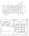
- FIG. 12is a simplified block diagram of a high-level organization of various embodiments of a memory device according to various embodiments of the present invention.
- FIG. 13is a simplified block diagram of a high-level organization of various embodiments of an electronic system according to the present invention.
- wafer and substrateare interchangeably used to refer generally to any structure on which integrated circuits are formed, and also to such structures during various stages of integrated circuit fabrication. Both terms include doped and undoped semiconductors, epitaxial layers of a semiconductor on a supporting semiconductor or insulating material, combinations of such layers, as well as other such structures that are known in the art.
- Various embodiments of the present inventionprovides methods to strain silicon, and structures formed using strained silicon.
- a crystalline semiconductor membraneis bonded to a crystalline semiconductor substrate at a predetermined misorientation to provide the membrane with a desired strain.
- Various embodimentsmechanically strain a thin silicon layer by bonding the thin silicon layer to a silicon substrate with a desired tilt misorientation to provide the silicon layer with a desired uniaxial strain.
- Various embodimentsmechanically strain a thin silicon layer by bonding the thin silicon layer to a silicon substrate with a desired twist misorientation to provide the silicon layer with a desired biaxial strain.
- Various embodimentsmechanically strain a thin silicon layer by bonding the thin silicon layer to a silicon substrate with a desired tilt and twist misorientation.
- the silicon layeris sufficiently thin such that it does not plastically deform due to dislocations, yields and/or fractures.
- Siis intentionally strained with a mechanical strain to enhance carrier mobility. Desirable mechanical strain can be determined using research findings for Si/SiGe structures.
- Sihas a lattice constant of 5.43095 ⁇
- Gehas a lattice constant of 5.64613 ⁇ .
- the lattice constant of SiGeis between the lattice constant of Si and the lattice constant of Ge, and depends on the percentage of Ge in the SiGe layer.
- FIG. 1illustrates the lattice constant of a Si 1 ⁇ X Ge X substrate for different percentages (X) of Ge. As indicated by FIG. 1 , a Si 1 ⁇ X Ge X substrate containing about 30% Ge (X ⁇ 0.3) has a lattice constant of about 5.50 ⁇ .
- the biaxial strain of the Si on the SiGecan be calculated as follows:
- Biaxial_StrainSiGe LC - Si LC Si LC ( 1 ) where the subscript LC represents the lattice constant of the SiGe or Si.
- the Si on the SiGe substratehas a biaxial strain of about 1.28%.
- FIG. 2illustrates the mobility enhancement for strained Si for different percentages (X) of Ge in a Si 1 ⁇ X Ge X substrate.
- the mobility enhancementincreases as the percentage of Ge in the Si 1 ⁇ X Ge X increases, and levels off to around 1.6 when the percentage of Ge is around 22% or larger.
- 22% Geprovides the Si 1 ⁇ X Ge X substrate with a lattice constant (SiGe LC ) of around 5.485.
- SiGe LClattice constant
- FIG. 3illustrates a relationship between elastic strain and semiconductor layer thicknesses. The semiconductor yield is plotted with respect to plastic deformation and defects in bulk samples. The illustrated values represent the relationship of thin SiGe layers on silicon.
- FIG. 3illustrates that thin layers of silicon or other semiconductor materials are more tolerant of strain than thick bulk samples. Previously, thin layers of SiGe have been fabricated on silicon because of the tolerance of the thin layers to strain.
- FIG. 3indicates that 1000 ⁇ thin semiconductor layers can be strained up to about 1%, that 100 ⁇ thin semiconductor layers can be strained up to about 2% and thinner semiconductor layers can be strained up to about 2.5%.
- a thin semiconductor layersuch as a silicon layer
- a strain greater than 0.5%it is desirable to strain a thin semiconductor layer, such as an ultra-thin silicon layer approximately 100 ⁇ or less, with a strain within a range of approximately 0.75% to approximately 1.5% where the mobility enhancement levels off. It is also desirable to reduce unnecessary strain and provide a margin for error without unduly affecting the mobility enhancement.
- a thin semiconductor layersuch as a thin silicon layer, with a strain in the range of approximately 1% to approximately 1.2%.
- a thin silicon filmis strained by bonding the thin silicon film on a silicon substrate with a predetermined misorientation.
- the predetermined misorientationis a predetermined tilt and/or twist misorientation. Twist-bonding has been explored in wafer bonding research, where it is known that a lattice-mismatch between an epitaxial layer and the substrate material causes structural defects when a film is grown to a certain thickness. The film grows pseudomorphically until dislocations form to accommodate the strain energy. Thus, misorientation during wafer bonding can cause a stress that results in plastic deformation. The stress associated with the misorientation causes dislocations to be created, and/or causes the bonded material to yield.
- a thin silicon filmis bonded on a silicon substrate with a predetermined misorientation (tilt and/or twist) to produce a sufficient strain for mobility enhancement without causing dislocations, plastic deformation, yield and/or fracture.
- a bond between a crystalline membrane and a crystalline substrateis designed with two or more strong body regions that are separated by a weak bonding region.
- the strong bonding regionsinclude a regular array of screw dislocations.
- the membrane in the weak bonding regionhas a desired strain.
- Various embodiments of the present inventionprovide biaxial-strained silicon and various embodiments provide uniaxial-strained silicon.
- FIG. 4illustrates bonding of a thin semiconductor film with respect to a substrate at a predetermined misorientation, according to various embodiments of the present invention.
- the figureillustrates a crystalline semiconductor substrate 402 , such as a crystalline semiconductor substrate, and further illustrates a crystalline thin semiconductor film 404 , layer or membrane, such as a crystalline silicon membrane.
- the membrane 404is oriented to the substrate 402 at an angle ⁇ , and is bonded to the substrate. Due to the crystalline nature of the membrane 404 and the substrate 402 , the crystal orientation of the membrane is considered to be misorientated with the crystal orientation of the substrate. This misorientation is intentional, and as is described below, is chosen to provide a desired strain in the membrane.
- the membrane and the substrateare defined to have strong bonding regions 406 and a weak bonding region 408 between the strong bonding regions.
- the nomenclature for these regions 406 and 408characterize a bonding interface between the membrane 404 and the substrate 402 .
- the membrane and the substrateare appropriately prepared to provide an oxide-free bonding interface between the membrane and the substrate in the strong bonding regions 406 to provide a stronger bond.
- the membrane and the substrateare appropriately prepared to provide an oxide in the bonding interface between the membrane and the substrate in the weak bonding region 408 to provide a weaker bond.
- the strong bonding regions 406have a regular array of screw dislocations that bond the membrane to the substrate.
- the membrane 404is strained in the weak bonding region 408 . A desired strain is achieved by controlling the misorientation angle ⁇ .
- Thinner semiconductor layersare capable of being under greater strain before yielding.
- the semiconductor membranehas a thickness such that it does not yield under a desired strain achieved by bonding the membrane to the substrate at a desired misorientation angle.
- the semiconductor membraneis ultra thin.
- the semiconductor membraneis approximately 1000 ⁇ or less. In various embodiments, the semiconductor membrane is approximately 100 ⁇ or less.
- One process for forming the membrane 404involves a bond cut process to form a surface silicon layer from a sacrificial wafer, and bond the surface silicon layer to a silicon substrate in a manner to provide the desired twist and/or tilt orientation between the crystalline structure in the surface layer and the crystalline structure in the substrate.
- the bond cut processhas been referred to in various literature as a “smart-cut process.”
- FIGS. 5A-5Dillustrate a method to form a strained semiconductor membrane using a bond cut process, according to various embodiments of the present invention.
- the bond cut processinvolves bonding together two substrates, or wafers, and breaking off a section of at least one of the two substrate after the substrates have been bonded together.
- FIG. 5Aillustrates a sacrificial semiconductor wafer 510
- FIG. 5Billustrates a semiconductor substrate 502
- the substrate 502includes a semiconductor material.
- the semiconductor materialincludes one of the following materials: silicon; germanium; silicon-germanium; gallium arsenide; indium phosphide; and other semiconductor materials. This list of potential semiconductor materials is not intended to be an all-inclusive list.
- the silicon substrateis cut into wafer size patterns, and integrated circuits are formed thereon.
- the sacrificial waferincludes various semiconductor material including but not limited to silicon, germanium, silicon-germanium, gallium arsenide, indium phosphide, and other semiconductor materials.
- the sacrificial wafer 510is a single crystal wafer, and is conditioned by implanting ions 512 into a surface.
- the ionsare implanted along a plane, represented in FIG. 6 as a line 514 , to define a surface layer 516 with a predetermined thickness.
- the planeis approximately parallel to the surface in which the ions are implanted.
- hydrogen ionsare used as implantation ions.
- the hydrogen ionscan include H + , H 2 + , D + , and/or D 2 + ions.
- the implanted ionsact 512 to form cavities along the plane 514 .
- the cavitiesare joined through thermal processing, allowing the surface layer 516 to be removed from the remaining portion of the sacrificial wafer 518 at the cleavage plane 514 .
- this thermal processingoccurs while the surface layer 516 is being bonded to the substrate 502 , as shown in FIG. 5C .
- the surface layerbreaks off of the sacrificial wafer at the cleavage plane and remains bonded to the substrate.
- the remaining portion of the sacrificial wafer 518can be used to form membranes for other substrates, thus reducing waste the overall cost for the manufacturing process of a wide variety of electronic devices.
- At least one of the membrane and the substrateare prepared to define strong and weak bond regions 506 and 508 , respectively.
- FIG. 5Billustrates an oxide 520 on the substrate 502 where it is desired to weakly bond the membrane to the substrate.
- the strong bonding regionsare oxide-free to provide strongly bond the interface of the membrane to the substrate.
- FIG. 5Cillustrates the surface layer 516 of the sacrificial wafer 510 bonded to the substrate 502 .
- the bonding forceincludes the strong Van der Waal's force that naturally bonds surfaces together as the bonding force.
- the Van der Waal's forceprovides an initial bonding force that is strengthened during subsequent thermal processing.
- the bonded wafersare heated to further bond the surface layer to the substrate and to cut the surface layer 516 from the sacrificial wafer 510 .
- Heating the sacrificial waferjoins the cavities in the cleavage plane, allowing the remaining portion of the sacrificial wafer to be removed from the surface layer, which remains bonded to the substrate.
- the remaining portion of the sacrificial wafercan be prepared and conditioned for another bond cut process.
- the thickness of the silicon layer 516 bonded to the substrate 502is defined by the depth of ion implantation 512 during the bond cut process. In various embodiments, the thickness of the silicon layer is such that it does not yield or otherwise plastically deform under the desired mechanical strained induced by the twist/tilt bond. In various embodiments, the silicon layer has a thickness of about 0.1 microns (100 nm or 1000 ⁇ ). In various embodiments, the silicon layer has a thickness less than 0.1 microns. In various embodiments, the silicon layer has a thickness of around 100 ⁇ or less.
- the silicon filmis prepared for transistor fabrication.
- the preparation of the filmincludes chemical and/or mechanical polishing.
- the membrane bonded to the substrate illustrated in FIG. 5Dcan be thinner than the surface layer defined in the sacrificial layer in FIG. 5A .
- Device processingcan be accomplished using conventional processes and procedures.
- FIGS. 6A-6Billustrate a method to biaxially strain a semiconductor membrane by bonding the membrane to the substrate at a predetermined twist misorientation, according to various embodiments of the present invention.
- the figureillustrates a top view of a silicon membrane 604 bonded to a silicon substrate 602 with a predetermined twist misorientation.
- the misorientation angle ais along the plane where the membrane 604 interfaces with the substrate 602 .
- the present inventionis applicable to semiconductor material other than silicon.
- Strong bonding regions 606are provided, and a weak boding region 608 is provided between the strong bonding regions 606 .
- the membrane 604or thin film, is pinned to the substrate in the strong bonding regions. These strong bonding regions are made free of an oxide.
- the weak bonding region between the pinned regions where the film will be strainedis left with a thin oxide or native oxide, or otherwise is provided with an oxide, to provide a low bonding strength.
- FIG. 6Bis a top view of the membrane that is pinned to the substrate in the strong bonding regions.
- the membrane in the weak bonding regionhas a biaxial strain, as indicated by the arrows 622 .
- FIGS. 7A-7Billustrate a method to uniaxially strain a semiconductor membrane by bonding the membrane to the substrate at a predetermined tilt misorientation, according to various embodiments of the present invention.
- FIG. 7Aillustrates a side view of a silicon membrane 704 bonded to a silicon substrate 702 with a predetermined tilt orientation.
- the misorientation angle ⁇is vertical with respect to a flat wafer surface.
- the present inventionis applicable to semiconductor material other than silicon.
- FIG. 7Billustrates a top view of the silicon layer.
- the siliconis uniaxially strained if the misorientation is attributed to a tilt misorientation.
- Strong bonding regions 706are provided, and a weak bonding region 708 is provided between the strong bonding regions.
- the membrane 704or thin film, is pinned to the substrate 702 in the strong bonding regions 706 . These strong bonding regions are made free of an oxide.
- the weak bonding region 708 between the pinned regions where the film will be strainedis left with a thin oxide or native oxide, or otherwise is provided with an oxide, to provide a low bonding strength.
- the membrane 704 in the weak bonding region 708has a uniaxial strain, as indicated by the arrows 724 .
- Uniaxial strained siliconreduces band gap and in-plane effective mass to improve conduction, reduces contact potentials, and alters the work function.
- FIG. 8illustrates a misorientation angle ( ⁇ ) for crystalline semiconductor cells having a length (a) for use to determine a strain associated with the misorientation.
- the figureillustrates a calculation of the amount of strain as a function of a twist misorientation. As is calculated below, 1.8° twist misorientation produces a 1% strain. This strain stretches the silicon bonds. A 1% strain is sufficient to produce a significant enhancement in the electron mobility. As provided earlier, a silicon strain greater than 0.5% achieves significant mobility enhancement.
- Various embodimentsprovide a strain up to about 2.5%.
- Various embodimentsmechanically strain the silicon with a strain within a range of approximately 0.75% to approximately 1.5% where the mobility enhancement levels off.
- Various embodimentsmechanically strain the silicon with a strain within a range of approximately 1% to approximately 1.2%.
- a thin silicon filmis bonded to a silicon substrate.
- the thin silicon filmapproximately 1000 ⁇ (100 nm) or less. Silicon films having a thickness of approximately 1000 ⁇ (100 nm) or less can be referred to as ultra-thin films.
- the thin silicon filmis approximately 100 ⁇ or less.
- the length of the crystalline atomsis identified as “a” and the length for a number (n) of crystalline atoms is “n ⁇ a.”
- the length of a number of crystalline atomsincreases from “n ⁇ a” to d when a crystalline membrane is bonded to a crystalline substrate with a misorientation angle ⁇ because the silicon bonds are stretched. Referring to the figure, it is determined that:
- the induced strainis approximately equal to one half the misorientation angle ⁇ in radians, where ⁇ is small.
- a 2.5% straincorresponds to a misorientation angle of 0.050 radians or 2.9°
- a 0.75% straincorresponds to a misorientation angle of 0.015 radians or 0.86°.
- FIG. 9illustrates a transistor fabricated with a strained semiconductor membrane, according to various embodiments of the present invention.
- the illustrated transistor 930includes a crystalline semiconductor substrate 902 , and a crystalline semiconductor membrane 904 bonded to the substrate 902 with a desired misorientation to provide the membrane 904 with a desired strain.
- a gate dielectric 932is formed on the strained membrane, and a gate 934 is formed on the gate dielectric 932 .
- First and second diffusion regions 936 and 938are formed in the structure.
- a channel region 940is formed in the strained semiconductor membrane 904 between the first and second diffusion regions 936 and 938 .
- FIG. 10illustrates a method for forming a strained semiconductor structure, according to various embodiments of the present invention.
- at least two strong bonding regionsare defined at 1050 for a desired bond between a crystalline semiconductor membrane and a crystalline semiconductor substrate.
- the strong bonding regionsare separated by a weak bonding region.
- the membraneis bonded to the substrate at a predetermined misorientation at 1052 .
- the membraneis pinned to the substrate at the strong bonding regions by a regular array of screw dislocations.
- the membraneis strained in the weak bonding region. The strain corresponds to the misorientation angle of the membrane bonded to the substrate.
- FIG. 11illustrates a method for forming a strained semiconductor structure using a bond cut process, according to various embodiments of the present invention.
- a membraneis defined in a surface layer of a sacrificial wafer. The membrane is defined by implanting ions into the surface layer of the sacrificial wafer to form cavities along a cleavage plane in the sacrificial wafer.
- the surface layer of the sacrificial waferis bonded to a substrate at two or more strong bonding regions in a predetermined misorientation. The naturally occurring Van der Waal's force provides an initial bonding force.
- the sacrificial wafer and the substrateis heat treated.
- This heat-treating processfurther bonds the surface layer of the sacrificial wafer to the substrate, and joins the cavities along the cleavage plane.
- the sacrificial wafer(or the remaining portions thereof) is removed from the membrane with the membrane left bonded to the substrate at the predetermined misorientation.
- the membranehas a desired strain in a weak bonding region positioned between strong bonding regions.
- FIG. 12is a simplified block diagram of a high-level organization of various embodiments of a memory device according to various embodiments of the present invention.
- the illustrated memory device 1268includes a memory array 1270 and read/write control circuitry 1272 to perform operations on the memory array via communication line(s) 1274 .
- the illustrated memory device 1268may be a memory card or a memory module such as a single inline memory module (SIMM) and dual inline memory module (DIMM).
- SIMMsingle inline memory module
- DIMMdual inline memory module
- the memory array 1270 and/or the control circuitry 1272include transistors with strained body layers formed using a strained silicon on silicon germanium (Si/SiGe) structure.
- Si/SiGestrained silicon on silicon germanium
- the memory array 1270includes a number of memory cells 1278 .
- the memory cells in the arrayare arranged in rows and columns.
- word lines 1280connect the memory cells in the rows
- bit lines 1282connect the memory cells in the columns.
- the read/write control circuitry 1272includes word line select circuitry 1274 , which functions to select a desired row.
- the read/write control circuitry 1272further includes bit line select circuitry 1276 , which functions to select a desired column.
- FIG. 13is a simplified block diagram of a high-level organization of various embodiments of an electronic system according to the present invention.
- the system 1300is a computer system, a process control system or other system that employs a processor and associated memory.
- the electronic system 1300has functional elements, including a processor or arithmetic/logic unit (ALU) 1302 , a control unit 1304 , a memory device unit 1306 (such as illustrated in FIG. 12 ) and an input/output (I/O) device 1308 .
- ALUarithmetic/logic unit
- control unit 1304such as illustrated in FIG. 12
- memory device unit 1306such as illustrated in FIG. 12
- I/Oinput/output
- Such an electronic system 1300will have a native set of instructions that specify operations to be performed on data by the processor 1302 and other interactions between the processor 1302 , the memory device unit 1306 and the I/O devices 1308 .
- the control unit 1304coordinates all operations of the processor 1302 , the memory device 1306 and the I/O devices 1308 by continuously cycling through a set of operations that cause instructions to be fetched from the memory device 1306 and executed.
- the memory device 1306includes, but is not limited to, random access memory (RAM) devices, read-only memory (ROM) devices, and peripheral devices such as a floppy disk drive and a compact disk CD-ROM drive.
- RAMrandom access memory
- ROMread-only memory
- peripheral devicessuch as a floppy disk drive and a compact disk CD-ROM drive.
- any of the illustrated electrical componentsare capable of being fabricated to include strained silicon on silicon germanium (Si/SiGe) in accordance with the present invention.
- the illustration of the system 1300is intended to provide a general understanding of one application for the structure and circuitry of the present invention, and is not intended to serve as a complete description of all the elements and features of an electronic system using strained semiconductor films according to the present invention.
- an electronic systemcan be fabricated in single-package processing units, or even on a single semiconductor chip, in order to reduce the communication time between the processor and the memory device.
- Applications containing strained semiconductor films, such as transistors with a strained semiconductor body layer, as described in this disclosureinclude electronic systems for use in memory modules, device drivers, power modules, communication modems, processor modules, and application-specific modules, and may include multilayer, multichip modules. Such circuitry can further be a subcomponent of a variety of electronic systems.
- the present inventionprovides strained semiconductor layers by bonding, or wafer bonding, a crystalline semiconductor membrane to a crystalline semiconductor substrate at a predetermined misorientation.
- the membraneis strongly bonded to the substrate in at least two strong bonding regions and is weakly bonded to the substrate in a weak bonding region between the strong bonding regions.
- the membrane in the weak bonding regionhas a strain attributable to the misorientation.
- a regular array of screw dislocationsbonds the membrane to the substrate in the strong bonding regions.
- an interface between the membrane and the substrateis free of an oxide in the strong bonding regions, and includes an oxide, such as a thin oxide or native oxide, in the weak bonding regions.
Landscapes
- Engineering & Computer Science (AREA)
- Physics & Mathematics (AREA)
- Microelectronics & Electronic Packaging (AREA)
- General Physics & Mathematics (AREA)
- Manufacturing & Machinery (AREA)
- Computer Hardware Design (AREA)
- Condensed Matter Physics & Semiconductors (AREA)
- Power Engineering (AREA)
- High Energy & Nuclear Physics (AREA)
- Health & Medical Sciences (AREA)
- Toxicology (AREA)
- Recrystallisation Techniques (AREA)
- Insulated Gate Type Field-Effect Transistor (AREA)
- Metal-Oxide And Bipolar Metal-Oxide Semiconductor Integrated Circuits (AREA)
Abstract
Description
where the subscript LC represents the lattice constant of the SiGe or Si. Thus, as shown in
Equation 6 is simplified into equation 7 as follows.
d=(n·a)·√{square root over (1+(tan2α).)} (7)
If “x” is small, the following approximation (equation 8) can be made.
Substituting into equation 7,
If α small, the following approximation (equation 11) can be made.
tan α≈α, (11)
where α is in radians. Substituting into equation 10,
An estimated strain when α is 1.15°, which equals π(1.15/180) or 0.02 radians, is provided in equation 13.
Thus, the induced strain is approximately equal to one half the misorientation angle α in radians, where α is small. Thus, a 2.5% strain corresponds to a misorientation angle of 0.050 radians or 2.9°, and a 0.75% strain corresponds to a misorientation angle of 0.015 radians or 0.86°.
Claims (28)
Priority Applications (1)
| Application Number | Priority Date | Filing Date | Title |
|---|---|---|---|
| US11/318,124US7429763B2 (en) | 2003-04-29 | 2005-12-23 | Memory with strained semiconductor by wafer bonding with misorientation |
Applications Claiming Priority (3)
| Application Number | Priority Date | Filing Date | Title |
|---|---|---|---|
| US10/425,484US7220656B2 (en) | 2003-04-29 | 2003-04-29 | Strained semiconductor by wafer bonding with misorientation |
| US10/931,749US7084429B2 (en) | 2003-04-29 | 2004-08-31 | Strained semiconductor by wafer bonding with misorientation |
| US11/318,124US7429763B2 (en) | 2003-04-29 | 2005-12-23 | Memory with strained semiconductor by wafer bonding with misorientation |
Related Parent Applications (1)
| Application Number | Title | Priority Date | Filing Date |
|---|---|---|---|
| US10/931,749DivisionUS7084429B2 (en) | 2003-04-29 | 2004-08-31 | Strained semiconductor by wafer bonding with misorientation |
Publications (2)
| Publication Number | Publication Date |
|---|---|
| US20060097281A1 US20060097281A1 (en) | 2006-05-11 |
| US7429763B2true US7429763B2 (en) | 2008-09-30 |
Family
ID=33309698
Family Applications (3)
| Application Number | Title | Priority Date | Filing Date |
|---|---|---|---|
| US10/425,484Expired - Fee RelatedUS7220656B2 (en) | 2003-04-29 | 2003-04-29 | Strained semiconductor by wafer bonding with misorientation |
| US10/931,749Expired - Fee RelatedUS7084429B2 (en) | 2003-04-29 | 2004-08-31 | Strained semiconductor by wafer bonding with misorientation |
| US11/318,124Expired - LifetimeUS7429763B2 (en) | 2003-04-29 | 2005-12-23 | Memory with strained semiconductor by wafer bonding with misorientation |
Family Applications Before (2)
| Application Number | Title | Priority Date | Filing Date |
|---|---|---|---|
| US10/425,484Expired - Fee RelatedUS7220656B2 (en) | 2003-04-29 | 2003-04-29 | Strained semiconductor by wafer bonding with misorientation |
| US10/931,749Expired - Fee RelatedUS7084429B2 (en) | 2003-04-29 | 2004-08-31 | Strained semiconductor by wafer bonding with misorientation |
Country Status (1)
| Country | Link |
|---|---|
| US (3) | US7220656B2 (en) |
Cited By (4)
| Publication number | Priority date | Publication date | Assignee | Title |
|---|---|---|---|---|
| US20040235264A1 (en)* | 2003-05-21 | 2004-11-25 | Micron Technology, Inc. | Gettering of silicon on insulator using relaxed silicon germanium epitaxial proximity layers |
| US20060244105A1 (en)* | 2003-07-21 | 2006-11-02 | Micron Technology, Inc. | Strained semiconductor by full wafer bonding |
| US8227309B2 (en) | 2006-02-16 | 2012-07-24 | Micron Technology, Inc. | Localized compressive strained semiconductor |
| US9379241B2 (en) | 2006-08-18 | 2016-06-28 | Micron Technology, Inc. | Semiconductor device with strained channels |
Families Citing this family (37)
| Publication number | Priority date | Publication date | Assignee | Title |
|---|---|---|---|---|
| EP1441445B1 (en)* | 2003-01-24 | 2006-11-29 | STMicroelectronics S.r.l. | A pipeline analog-to-digital converter with correction of inter-stage gain errors |
| US7198974B2 (en)* | 2003-03-05 | 2007-04-03 | Micron Technology, Inc. | Micro-mechanically strained semiconductor film |
| US7220656B2 (en)* | 2003-04-29 | 2007-05-22 | Micron Technology, Inc. | Strained semiconductor by wafer bonding with misorientation |
| US7041575B2 (en)* | 2003-04-29 | 2006-05-09 | Micron Technology, Inc. | Localized strained semiconductor on insulator |
| US6987037B2 (en)* | 2003-05-07 | 2006-01-17 | Micron Technology, Inc. | Strained Si/SiGe structures by ion implantation |
| US7115480B2 (en)* | 2003-05-07 | 2006-10-03 | Micron Technology, Inc. | Micromechanical strained semiconductor by wafer bonding |
| US7501329B2 (en) | 2003-05-21 | 2009-03-10 | Micron Technology, Inc. | Wafer gettering using relaxed silicon germanium epitaxial proximity layers |
| US7273788B2 (en) | 2003-05-21 | 2007-09-25 | Micron Technology, Inc. | Ultra-thin semiconductors bonded on glass substrates |
| US7008854B2 (en)* | 2003-05-21 | 2006-03-07 | Micron Technology, Inc. | Silicon oxycarbide substrates for bonded silicon on insulator |
| US7153753B2 (en)* | 2003-08-05 | 2006-12-26 | Micron Technology, Inc. | Strained Si/SiGe/SOI islands and processes of making same |
| US7495266B2 (en)* | 2004-06-16 | 2009-02-24 | Massachusetts Institute Of Technology | Strained silicon-on-silicon by wafer bonding and layer transfer |
| US7465992B2 (en)* | 2005-04-27 | 2008-12-16 | International Business Machines Corporation | Field effect transistor with mixed-crystal-orientation channel and source/drain regions |
| WO2007019487A2 (en)* | 2005-08-05 | 2007-02-15 | Reveo, Inc. | Method and system for fabricating thin devices |
| US7566949B2 (en)* | 2006-04-28 | 2009-07-28 | International Business Machines Corporation | High performance 3D FET structures, and methods for forming the same using preferential crystallographic etching |
| DE102006019835B4 (en)* | 2006-04-28 | 2011-05-12 | Advanced Micro Devices, Inc., Sunnyvale | Transistor having a channel with tensile strain oriented along a crystallographic orientation with increased charge carrier mobility |
| US7485544B2 (en)* | 2006-08-02 | 2009-02-03 | Micron Technology, Inc. | Strained semiconductor, devices and systems and methods of formation |
| US8962447B2 (en)* | 2006-08-03 | 2015-02-24 | Micron Technology, Inc. | Bonded strained semiconductor with a desired surface orientation and conductance direction |
| US7759233B2 (en)* | 2007-03-23 | 2010-07-20 | Micron Technology, Inc. | Methods for stressing semiconductor material structures to improve electron and/or hole mobility of transistor channels fabricated therefrom, and semiconductor devices including such structures |
| US8293611B2 (en) | 2007-05-08 | 2012-10-23 | Micron Technology, Inc. | Implantation processes for straining transistor channels of semiconductor device structures and semiconductor devices with strained transistor channels |
| DE102010046215B4 (en) | 2010-09-21 | 2019-01-03 | Infineon Technologies Austria Ag | Semiconductor body with strained region, electronic component and a method for producing the semiconductor body. |
| US10543662B2 (en) | 2012-02-08 | 2020-01-28 | Corning Incorporated | Device modified substrate article and methods for making |
| US9340443B2 (en) | 2012-12-13 | 2016-05-17 | Corning Incorporated | Bulk annealing of glass sheets |
| US10014177B2 (en) | 2012-12-13 | 2018-07-03 | Corning Incorporated | Methods for processing electronic devices |
| TWI617437B (en) | 2012-12-13 | 2018-03-11 | 康寧公司 | Facilitated processing for controlling bonding between sheet and carrier |
| US10086584B2 (en) | 2012-12-13 | 2018-10-02 | Corning Incorporated | Glass articles and methods for controlled bonding of glass sheets with carriers |
| US10510576B2 (en) | 2013-10-14 | 2019-12-17 | Corning Incorporated | Carrier-bonding methods and articles for semiconductor and interposer processing |
| CN106132688B (en) | 2014-01-27 | 2020-07-14 | 康宁股份有限公司 | Article and method for controlled bonding of a sheet to a carrier |
| EP3129221A1 (en) | 2014-04-09 | 2017-02-15 | Corning Incorporated | Device modified substrate article and methods for making |
| EP2933824B1 (en)* | 2014-04-14 | 2021-08-18 | Nxp B.V. | Substrate arrangement |
| US9263586B2 (en) | 2014-06-06 | 2016-02-16 | Taiwan Semiconductor Manufacturing Company, Ltd. | Quantum well fin-like field effect transistor (QWFinFET) having a two-section combo QW structure |
| EP3297824A1 (en) | 2015-05-19 | 2018-03-28 | Corning Incorporated | Articles and methods for bonding sheets with carriers |
| KR102524620B1 (en) | 2015-06-26 | 2023-04-21 | 코닝 인코포레이티드 | Methods and articles including sheets and carriers |
| TW201825623A (en) | 2016-08-30 | 2018-07-16 | 美商康寧公司 | Peptide plasma polymer for sheet bonding |
| TWI821867B (en) | 2016-08-31 | 2023-11-11 | 美商康寧公司 | Articles of controllably bonded sheets and methods for making same |
| JP7260523B2 (en) | 2017-08-18 | 2023-04-18 | コーニング インコーポレイテッド | Temporary binding using polycationic polymers |
| US11331692B2 (en) | 2017-12-15 | 2022-05-17 | Corning Incorporated | Methods for treating a substrate and method for making articles comprising bonded sheets |
| US12328913B1 (en)* | 2021-06-10 | 2025-06-10 | Unm Rainforest Innovations | Vertical spintronic devices based on dislocations in single-crystalline semiconductors and methods for their production |
Citations (43)
| Publication number | Priority date | Publication date | Assignee | Title |
|---|---|---|---|---|
| JPS54155770A (en) | 1978-05-29 | 1979-12-08 | Nec Corp | Manufacture of semiconductor device |
| US5234535A (en) | 1992-12-10 | 1993-08-10 | International Business Machines Corporation | Method of producing a thin silicon-on-insulator layer |
| US5441591A (en) | 1993-06-07 | 1995-08-15 | The United States Of America As Represented By The Secretary Of The Navy | Silicon to sapphire bond |
| US5461243A (en) | 1993-10-29 | 1995-10-24 | International Business Machines Corporation | Substrate for tensilely strained semiconductor |
| US5854501A (en) | 1995-11-20 | 1998-12-29 | Micron Technology, Inc. | Floating gate semiconductor device having a portion formed with a recess |
| US5879996A (en) | 1996-09-18 | 1999-03-09 | Micron Technology, Inc. | Silicon-germanium devices for CMOS formed by ion implantation and solid phase epitaxial regrowth |
| US5963817A (en) | 1997-10-16 | 1999-10-05 | International Business Machines Corporation | Bulk and strained silicon on insulator using local selective oxidation |
| US6103598A (en) | 1995-07-13 | 2000-08-15 | Canon Kabushiki Kaisha | Process for producing semiconductor substrate |
| US6136666A (en) | 1998-06-30 | 2000-10-24 | Hyundai Electronics Industries Co., Ltd. | Method for fabricating silicon-on-insulator wafer |
| US6143628A (en) | 1997-03-27 | 2000-11-07 | Canon Kabushiki Kaisha | Semiconductor substrate and method of manufacturing the same |
| US6228694B1 (en) | 1999-06-28 | 2001-05-08 | Intel Corporation | Method of increasing the mobility of MOS transistors by use of localized stress regions |
| US6423613B1 (en) | 1998-11-10 | 2002-07-23 | Micron Technology, Inc. | Low temperature silicon wafer bond process with bulk material bond strength |
| US20020185686A1 (en) | 2001-06-12 | 2002-12-12 | International Business Machines Corporation | Relaxed SiGe layers on Si or silicon-on-insulator substrates by ion implantation and thermal annealing |
| US20030013323A1 (en) | 2001-06-14 | 2003-01-16 | Richard Hammond | Method of selective removal of SiGe alloys |
| US6514836B2 (en) | 2001-06-04 | 2003-02-04 | Rona Elizabeth Belford | Methods of producing strained microelectronic and/or optical integrated and discrete devices |
| US6515335B1 (en) | 2002-01-04 | 2003-02-04 | International Business Machines Corporation | Method for fabrication of relaxed SiGe buffer layers on silicon-on-insulators and structures containing the same |
| US6583437B2 (en) | 2000-03-17 | 2003-06-24 | Kabushiki Kaisha Toshiba | Semiconductor device and method of manufacturing the same |
| US6649492B2 (en) | 2002-02-11 | 2003-11-18 | International Business Machines Corporation | Strained Si based layer made by UHV-CVD, and devices therein |
| US20030218189A1 (en) | 2001-06-12 | 2003-11-27 | International Business Machines Corporation | Relaxed SiGe layers on Si or silicon-on-insulator substrates by ion implantation and thermal annealing |
| US6657276B1 (en) | 2001-12-10 | 2003-12-02 | Advanced Micro Devices, Inc. | Shallow trench isolation (STI) region with high-K liner and method of formation |
| US6689671B1 (en) | 2002-05-22 | 2004-02-10 | Advanced Micro Devices, Inc. | Low temperature solid-phase epitaxy fabrication process for MOS devices built on strained semiconductor substrate |
| US6703648B1 (en) | 2002-10-29 | 2004-03-09 | Advanced Micro Devices, Inc. | Strained silicon PMOS having silicon germanium source/drain extensions and method for its fabrication |
| US6703293B2 (en) | 2002-07-11 | 2004-03-09 | Sharp Laboratories Of America, Inc. | Implantation at elevated temperatures for amorphization re-crystallization of Si1-xGex films on silicon substrates |
| US6740913B2 (en) | 1999-06-28 | 2004-05-25 | Intel Corporation | MOS transistor using mechanical stress to control short channel effects |
| US20040173798A1 (en) | 2003-03-05 | 2004-09-09 | Micron Technology, Inc. | Micro-mechanically strained semiconductor film |
| US20040214366A1 (en) | 2001-07-25 | 2004-10-28 | Nantero, Inc. | Electromechanical memory array using nanotube ribbons and method for making same |
| US6812508B2 (en) | 2000-11-28 | 2004-11-02 | Sharp Kabushiki Kaisha | Semiconductor substrate and method for fabricating the same |
| US20040217391A1 (en) | 2003-04-29 | 2004-11-04 | Micron Technology, Inc. | Localized strained semiconductor on insulator |
| US20040224480A1 (en) | 2003-05-07 | 2004-11-11 | Micron Technology, Inc. | Micromechanical strained semiconductor by wafer bonding |
| US20040232422A1 (en) | 2003-05-21 | 2004-11-25 | Micron Technology, Inc. | Wafer gettering using relaxed silicon germanium epitaxial proximity layers |
| US20040232488A1 (en) | 2003-05-21 | 2004-11-25 | Micron Technology, Inc. | Silicon oxycarbide substrates for bonded silicon on insulator |
| US20040232487A1 (en) | 2003-05-21 | 2004-11-25 | Micron Technology, Inc. | Ultra-thin semiconductors bonded on glass substrates |
| US20050020094A1 (en) | 2003-07-21 | 2005-01-27 | Micron Technology, Inc. | Strained semiconductor by full wafer bonding |
| US20050029619A1 (en) | 2003-08-05 | 2005-02-10 | Micron Technology, Inc. | Strained Si/SiGe/SOI islands and processes of making same |
| US6902616B1 (en) | 1995-07-19 | 2005-06-07 | Semiconductor Energy Laboratory Co., Ltd. | Method and apparatus for producing semiconductor device |
| US20050285139A1 (en) | 2003-05-07 | 2005-12-29 | Micron Technology, Inc. | Strained Si/SiGe structures by ion implantation |
| US6994762B2 (en) | 2003-02-10 | 2006-02-07 | The Boeing Company | Single crystal piezo (SCP) apparatus and method of forming same |
| US7081395B2 (en) | 2003-05-23 | 2006-07-25 | Taiwan Semiconductor Manufacturing Co., Ltd. | Silicon strain engineering accomplished via use of specific shallow trench isolation fill materials |
| US7084429B2 (en) | 2003-04-29 | 2006-08-01 | Micron, Technology, Inc. | Strained semiconductor by wafer bonding with misorientation |
| US20060258063A1 (en) | 2003-05-21 | 2006-11-16 | Micron Technology, Inc. | Gettering of silicon on insulator using relaxed silicon germanium epitaxial proximity layers |
| US20070075401A1 (en) | 2003-07-21 | 2007-04-05 | Micron Technology, Inc. | Gettering using voids formed by surface transformation |
| US20070096193A1 (en) | 2005-10-27 | 2007-05-03 | Micron Technology, Inc. | Non-volatile memory device with tensile strained silicon layer |
| US20080029840A1 (en) | 2006-08-02 | 2008-02-07 | Micron Technology, Inc. | Strained semiconductor, devices and systems and methods of formation |
Family Cites Families (6)
| Publication number | Priority date | Publication date | Assignee | Title |
|---|---|---|---|---|
| KR0157342B1 (en) | 1995-06-09 | 1998-12-01 | 김광호 | Voltage sensing method of nonvolatile semiconductor memory |
| JP3114643B2 (en) | 1997-02-20 | 2000-12-04 | 日本電気株式会社 | Semiconductor substrate structure and manufacturing method |
| US6093623A (en) | 1998-08-04 | 2000-07-25 | Micron Technology, Inc. | Methods for making silicon-on-insulator structures |
| US6242324B1 (en)* | 1999-08-10 | 2001-06-05 | The United States Of America As Represented By The Secretary Of The Navy | Method for fabricating singe crystal materials over CMOS devices |
| US6455397B1 (en) | 1999-11-16 | 2002-09-24 | Rona E. Belford | Method of producing strained microelectronic and/or optical integrated and discrete devices |
| US6586761B2 (en) | 2001-09-07 | 2003-07-01 | Intel Corporation | Phase change material memory device |
- 2003
- 2003-04-29USUS10/425,484patent/US7220656B2/ennot_activeExpired - Fee Related
- 2004
- 2004-08-31USUS10/931,749patent/US7084429B2/ennot_activeExpired - Fee Related
- 2005
- 2005-12-23USUS11/318,124patent/US7429763B2/ennot_activeExpired - Lifetime
Patent Citations (74)
| Publication number | Priority date | Publication date | Assignee | Title |
|---|---|---|---|---|
| JPS54155770A (en) | 1978-05-29 | 1979-12-08 | Nec Corp | Manufacture of semiconductor device |
| US5234535A (en) | 1992-12-10 | 1993-08-10 | International Business Machines Corporation | Method of producing a thin silicon-on-insulator layer |
| US5441591A (en) | 1993-06-07 | 1995-08-15 | The United States Of America As Represented By The Secretary Of The Navy | Silicon to sapphire bond |
| US5461243A (en) | 1993-10-29 | 1995-10-24 | International Business Machines Corporation | Substrate for tensilely strained semiconductor |
| US5759898A (en) | 1993-10-29 | 1998-06-02 | International Business Machines Corporation | Production of substrate for tensilely strained semiconductor |
| US6103598A (en) | 1995-07-13 | 2000-08-15 | Canon Kabushiki Kaisha | Process for producing semiconductor substrate |
| US6902616B1 (en) | 1995-07-19 | 2005-06-07 | Semiconductor Energy Laboratory Co., Ltd. | Method and apparatus for producing semiconductor device |
| US5854501A (en) | 1995-11-20 | 1998-12-29 | Micron Technology, Inc. | Floating gate semiconductor device having a portion formed with a recess |
| US5879996A (en) | 1996-09-18 | 1999-03-09 | Micron Technology, Inc. | Silicon-germanium devices for CMOS formed by ion implantation and solid phase epitaxial regrowth |
| US6143628A (en) | 1997-03-27 | 2000-11-07 | Canon Kabushiki Kaisha | Semiconductor substrate and method of manufacturing the same |
| US6251751B1 (en) | 1997-10-16 | 2001-06-26 | International Business Machines Corporation | Bulk and strained silicon on insulator using local selective oxidation |
| US5963817A (en) | 1997-10-16 | 1999-10-05 | International Business Machines Corporation | Bulk and strained silicon on insulator using local selective oxidation |
| US6136666A (en) | 1998-06-30 | 2000-10-24 | Hyundai Electronics Industries Co., Ltd. | Method for fabricating silicon-on-insulator wafer |
| US6630713B2 (en) | 1998-11-10 | 2003-10-07 | Micron Technology, Inc. | Low temperature silicon wafer bond process with bulk material bond strength |
| US6423613B1 (en) | 1998-11-10 | 2002-07-23 | Micron Technology, Inc. | Low temperature silicon wafer bond process with bulk material bond strength |
| US6228694B1 (en) | 1999-06-28 | 2001-05-08 | Intel Corporation | Method of increasing the mobility of MOS transistors by use of localized stress regions |
| US6740913B2 (en) | 1999-06-28 | 2004-05-25 | Intel Corporation | MOS transistor using mechanical stress to control short channel effects |
| US6583437B2 (en) | 2000-03-17 | 2003-06-24 | Kabushiki Kaisha Toshiba | Semiconductor device and method of manufacturing the same |
| US6812508B2 (en) | 2000-11-28 | 2004-11-02 | Sharp Kabushiki Kaisha | Semiconductor substrate and method for fabricating the same |
| US6514836B2 (en) | 2001-06-04 | 2003-02-04 | Rona Elizabeth Belford | Methods of producing strained microelectronic and/or optical integrated and discrete devices |
| US20020185686A1 (en) | 2001-06-12 | 2002-12-12 | International Business Machines Corporation | Relaxed SiGe layers on Si or silicon-on-insulator substrates by ion implantation and thermal annealing |
| US20030201468A1 (en) | 2001-06-12 | 2003-10-30 | Christiansen Silke H. | Relaxed SiGe layers on Si or silicon-on-insulator substrates by ion implantation and thermal annealing |
| US6593625B2 (en) | 2001-06-12 | 2003-07-15 | International Business Machines Corporation | Relaxed SiGe layers on Si or silicon-on-insulator substrates by ion implantation and thermal annealing |
| US20030218189A1 (en) | 2001-06-12 | 2003-11-27 | International Business Machines Corporation | Relaxed SiGe layers on Si or silicon-on-insulator substrates by ion implantation and thermal annealing |
| US20030013323A1 (en) | 2001-06-14 | 2003-01-16 | Richard Hammond | Method of selective removal of SiGe alloys |
| US20040214366A1 (en) | 2001-07-25 | 2004-10-28 | Nantero, Inc. | Electromechanical memory array using nanotube ribbons and method for making same |
| US6657276B1 (en) | 2001-12-10 | 2003-12-02 | Advanced Micro Devices, Inc. | Shallow trench isolation (STI) region with high-K liner and method of formation |
| US6515335B1 (en) | 2002-01-04 | 2003-02-04 | International Business Machines Corporation | Method for fabrication of relaxed SiGe buffer layers on silicon-on-insulators and structures containing the same |
| US6649492B2 (en) | 2002-02-11 | 2003-11-18 | International Business Machines Corporation | Strained Si based layer made by UHV-CVD, and devices therein |
| US6689671B1 (en) | 2002-05-22 | 2004-02-10 | Advanced Micro Devices, Inc. | Low temperature solid-phase epitaxy fabrication process for MOS devices built on strained semiconductor substrate |
| US6703293B2 (en) | 2002-07-11 | 2004-03-09 | Sharp Laboratories Of America, Inc. | Implantation at elevated temperatures for amorphization re-crystallization of Si1-xGex films on silicon substrates |
| US6703648B1 (en) | 2002-10-29 | 2004-03-09 | Advanced Micro Devices, Inc. | Strained silicon PMOS having silicon germanium source/drain extensions and method for its fabrication |
| US6994762B2 (en) | 2003-02-10 | 2006-02-07 | The Boeing Company | Single crystal piezo (SCP) apparatus and method of forming same |
| US20060011982A1 (en) | 2003-03-05 | 2006-01-19 | Micron Technology, Inc. | Micro-mechanically strained semiconductor film |
| US20040173798A1 (en) | 2003-03-05 | 2004-09-09 | Micron Technology, Inc. | Micro-mechanically strained semiconductor film |
| US20070164361A1 (en) | 2003-03-05 | 2007-07-19 | Micron Technology, Inc. | Micro-mechanically strained semiconductor film |
| US7202530B2 (en) | 2003-03-05 | 2007-04-10 | Micron Technology, Inc. | Micro-mechanically strained semiconductor film |
| US7198974B2 (en) | 2003-03-05 | 2007-04-03 | Micron Technology, Inc. | Micro-mechanically strained semiconductor film |
| US20040217391A1 (en) | 2003-04-29 | 2004-11-04 | Micron Technology, Inc. | Localized strained semiconductor on insulator |
| US7084429B2 (en) | 2003-04-29 | 2006-08-01 | Micron, Technology, Inc. | Strained semiconductor by wafer bonding with misorientation |
| US7041575B2 (en) | 2003-04-29 | 2006-05-09 | Micron Technology, Inc. | Localized strained semiconductor on insulator |
| US7023051B2 (en) | 2003-04-29 | 2006-04-04 | Micron Technology, Inc. | Localized strained semiconductor on insulator |
| US20050023616A1 (en) | 2003-04-29 | 2005-02-03 | Micron Technology, Inc. | Localized strained semiconductor on insulator |
| US7220656B2 (en) | 2003-04-29 | 2007-05-22 | Micron Technology, Inc. | Strained semiconductor by wafer bonding with misorientation |
| US20060208343A1 (en) | 2003-05-07 | 2006-09-21 | Micron Technology, Inc. | Micromechanical strained semiconductor by wafer bonding |
| US7045874B2 (en) | 2003-05-07 | 2006-05-16 | Micron Technology, Inc. | Micromechanical strained semiconductor by wafer bonding |
| US20040224480A1 (en) | 2003-05-07 | 2004-11-11 | Micron Technology, Inc. | Micromechanical strained semiconductor by wafer bonding |
| US20050285139A1 (en) | 2003-05-07 | 2005-12-29 | Micron Technology, Inc. | Strained Si/SiGe structures by ion implantation |
| US7115480B2 (en) | 2003-05-07 | 2006-10-03 | Micron Technology, Inc. | Micromechanical strained semiconductor by wafer bonding |
| US20050032296A1 (en) | 2003-05-07 | 2005-02-10 | Micron Technology, Inc. | Micromechanical strained semiconductor by wafer bonding |
| US6987037B2 (en) | 2003-05-07 | 2006-01-17 | Micron Technology, Inc. | Strained Si/SiGe structures by ion implantation |
| US20050023612A1 (en) | 2003-05-21 | 2005-02-03 | Micron Technology, Inc. | Ultra-thin semiconductors bonded on glass substrates |
| US7273788B2 (en) | 2003-05-21 | 2007-09-25 | Micron Technology, Inc. | Ultra-thin semiconductors bonded on glass substrates |
| US20040232487A1 (en) | 2003-05-21 | 2004-11-25 | Micron Technology, Inc. | Ultra-thin semiconductors bonded on glass substrates |
| US7271445B2 (en) | 2003-05-21 | 2007-09-18 | Micron Technology, Inc. | Ultra-thin semiconductors bonded on glass substrates |
| US7008854B2 (en) | 2003-05-21 | 2006-03-07 | Micron Technology, Inc. | Silicon oxycarbide substrates for bonded silicon on insulator |
| US20060001094A1 (en) | 2003-05-21 | 2006-01-05 | Micron Technology, Inc. | Semiconductor on insulator structure |
| US20060258123A1 (en) | 2003-05-21 | 2006-11-16 | Micron Technology, Inc. | Wafer gettering using relaxed silicon germanium epitaxial proximity layers |
| US20060258063A1 (en) | 2003-05-21 | 2006-11-16 | Micron Technology, Inc. | Gettering of silicon on insulator using relaxed silicon germanium epitaxial proximity layers |
| US20060263994A1 (en) | 2003-05-21 | 2006-11-23 | Micron Technology, Inc. | Semiconductors bonded on glass substrates |
| US20040232422A1 (en) | 2003-05-21 | 2004-11-25 | Micron Technology, Inc. | Wafer gettering using relaxed silicon germanium epitaxial proximity layers |
| US20040232488A1 (en) | 2003-05-21 | 2004-11-25 | Micron Technology, Inc. | Silicon oxycarbide substrates for bonded silicon on insulator |
| US7081395B2 (en) | 2003-05-23 | 2006-07-25 | Taiwan Semiconductor Manufacturing Co., Ltd. | Silicon strain engineering accomplished via use of specific shallow trench isolation fill materials |
| US20070075401A1 (en) | 2003-07-21 | 2007-04-05 | Micron Technology, Inc. | Gettering using voids formed by surface transformation |
| US20070080335A1 (en) | 2003-07-21 | 2007-04-12 | Micron Technology, Inc. | Gettering using voids formed by surface transformation |
| US20060244105A1 (en) | 2003-07-21 | 2006-11-02 | Micron Technology, Inc. | Strained semiconductor by full wafer bonding |
| US20050020094A1 (en) | 2003-07-21 | 2005-01-27 | Micron Technology, Inc. | Strained semiconductor by full wafer bonding |
| US7326597B2 (en) | 2003-07-21 | 2008-02-05 | Micron Technology, Inc. | Gettering using voids formed by surface transformation |
| US7153753B2 (en) | 2003-08-05 | 2006-12-26 | Micron Technology, Inc. | Strained Si/SiGe/SOI islands and processes of making same |
| US20060267152A1 (en) | 2003-08-05 | 2006-11-30 | Micron Technology, Inc. | Strained Si/SiGe/SOI islands and processes of making same |
| US7262428B2 (en) | 2003-08-05 | 2007-08-28 | Micron Technology, Inc. | Strained Si/SiGe/SOI islands and processes of making same |
| US20050029619A1 (en) | 2003-08-05 | 2005-02-10 | Micron Technology, Inc. | Strained Si/SiGe/SOI islands and processes of making same |
| US20070096193A1 (en) | 2005-10-27 | 2007-05-03 | Micron Technology, Inc. | Non-volatile memory device with tensile strained silicon layer |
| US20080029840A1 (en) | 2006-08-02 | 2008-02-07 | Micron Technology, Inc. | Strained semiconductor, devices and systems and methods of formation |
Non-Patent Citations (50)
| Title |
|---|
| "Cornell Demonstrates a Universal Substrate", Compound Semiconductor, 3(2), (Mar./Apr. 1997),27-29. |
| Abe, T , "Silicon Wafer-Bonding Process Technology for SOI Structures", Extended Abstracts of the 22nd (1990 International) Conference on Solid State Devices and Materials, (1990),853-856. |
| Ang, Kah W., "Enhanced performance in 50 nm N-MOSFETs with silicon-carbon source/drain regions", IEEE International Electron Devices Meeting, 2004. IEDM Technical Digest., (Dec. 2004), 1069-1071. |
| Auberton-Herve, A J., "SOI: Materials to Systems", International Electron Devices Meeting. Technical Digest, (1996),3-10. |
| Autumn, Kellar , et al., "Adhesive force of a single gecko foot-hair", Nature, 405(6787), (Jun. 2000),681-685. |
| Autumn, Kellar , et al., "Evidence for van der Waals adhesion in gecko setae.", Proceedings of the National Academy of Science U S A.; 99(19), (Sep. 17, 2002),12252-6. |
| Belford, Rona E., et al., "Performance-Augmented CMOS Using Back-End Uniaxial Strain", IEEE 60th DRC. Conference Digest Device Research Conference, 2002, (Jun. 24-26, 2002),41-42. |
| Berti, M. , "Composition and Structure of Si-Ge Layers Produced by Ion Implantation and Laser Melting", Journal of Materials Research, 6(10), (Oct. 1991),2120-2126. |
| Berti, M. , "Laser Induced Epitaxial Regrowth of Si[sub 1-3]Ge[sub x]/Si Layers Produced by Ge Ion Implantation", Applied Surface Science, 43, (1989),158-164. |
| Biever, Celeste , "Secret of 'strained silicon' revealed: behind closed doors, Intel has perfected a novel way to improve chip performance.", New Scientist, 180(i2426-2428), (Dec. 20, 2003),27. |
| Brown, Chappell , "Bonding twist hints at universal substrate", EETimes, (1997),2 pages. |
| Bruel, M , "Smart-Cut: a new silicon on insulator material technology based on hydrogen implantation and wafer bonding", Japanese Journal of Applied Physics, Part 1 (Regular Papers, Short Notes & Review Papers), 36(3B), (1997),1636-1641. |
| Cartagena, E. , "Bonded Etchback Silicon on Sapphire Bipolar Junction Transistors", Extended Abstracts-Electrochemical Society (1), Program and Abstracts: 183rd Meeting of the Electrochemical Society, Pennington, NJ,(1993),1199-1200. |
| Chilton, B T., et al., "Solid phase epitaxial regrowth of strained Si(1-x)Ge(x)/Si strained layer structures amorphized by ion implantation", Applied Physics Letters, 54(1), (Jan. 2, 1989),42-44. |
| Clark, Don , et al., "Intel unveils tiny new transistors: Process handles circuits 1/2000th the width of a human hair", The Wall Street Journal, (Aug. 13, 2002),3 pages. |
| Clifton, P A., et al., "A process for strained silicon n-channel HMOSFETs", ESSDERC'96. Proceedings of the 26th European Solid State Device Research Conference, (Sep. 1996),519-22. |
| Dharmatilleke, S N., et al., "Anodic Bonding of Glass to Glass and Silicon to Glass or Silicon to Silicon Through a Very Thick Thermally Grown SiO2 Layer", Proceedings of IS 3M International Symposium on Smart Structures and Microsystems, http://dolphin.eng.uc.edu/projects/bonding/paper.pdf,(2000),32. |
| Dubbelday, W B., et al., "Oscillatory strain relaxation in solid phase epitaxially regrown silicon on sapphire", Proceedings of the First International Workshop Lattice Mismatched Thin Films, (Sep. 13-15, 1998),13-17. |
| Fischetti, M V., et al., "Band structure, deformation potentials, and carrier mobility in strained Si, Ge, and SiGe alloys", Journal of Applied Physics, 80(4), (Aug. 15, 1996),2234-2252. |
| Fournel, F , et al., "Ultra High Precision Of The Tilt/Twist Misorientation Angles In Silicon/Silicon Direct Wafer Bonding", Abstract-Electronic Materials Conference, (Jun. 2002),9. |
| Garcia, G A., et al., "High-quality CMOS in thin (100 nm) silicon on sapphire", IEEE Electron Device Letters, 9(1), (Jan. 1988),32-34. |
| Ghani, T. , "A 90nm High Volume Manufacturing Logic Technology Featuring Novel 45nm Gate Length Strained Silicon CMOS Transistors", Technical Digest IEEE International Electron Devices Meeting, (Dec. 2003),978-980. |
| Goto, K. , "Technology Booster using Strain-Enhancing Laminated SiN (SELS) for 65nm Node Hp MPUs", IEDM Technical Digest. IEEE International Electron Devices Meeting, (Dec. 2004),209-212. |
| Harendt, Christine , "Silicon on Insulator Material by Wafer Bonding", Journal of Electronic Materials, 20(3), (Mar. 1991),267-77. |
| Imthurn, George P., et al., "Bonded Silicon-on-Sapphire Wafers and Devices", Journal of Applied Physics, 72(6), (Sep. 1992),2526-7. |
| Irie, H. , et al., "In-plane mobility anisotropy and university under uni-axial strains in nand p-MOS inversion layers on (100), [110], and (111) Si" IEEE International Electron Devices Meeting, 2004. IEDM Technical Digest., (Dec. 2004),225-228. |
| Komoda, Y. , "Mobility Improvement for 45nm Node by Combination of Optimized Stress Control and Channel Orientation Design", IEEE International Electron Devices Meeting, 2004. IEDM Technical Digest., (Dec. 2004),217-220. |
| Kostrzewa, M , et al., "Testing the Feasibility of strain relaxed InAsP and InGaAs compliant substrates", EMC 2003 International Conference Indium Phosphide and Related Materials. Conference Proceedings, (Jun. 2003),8. |
| Lasky, J. B., "Wafer Bonding for Silicon-on-Insulator Technologies", Applied Physics Letters, 48(1), (Jan. 6, 1986),78-80. |
| Lu, D, , "Bonding Silicon Wafers by Use of Electrostatic Fields Followed by Rapid Thermal Heating", Materials Letters, 4(11), (Oct. 1986),461-464. |
| Maikas, S. , "Package-strain-enhanced device and circuit performance", IEEE International Electron Devices Meeting, 2004. IEDM Technical Digest., (Dec. 2004),233-236. |
| Mizuno, T , et al., "Advanced SOI-MOSFETs with Strained-Si Channel for High Speed CMOS Electron/Hole Mobility Enhancement", 2000 Symposium on VLSI Technology, Digest of Technical Papers, (2000),210-211. |
| Moran, Peter , "Strain Relaxation in Wafer-Bonded SiGe/Si Heterostructures Due to Viscous Flow of an Underlying Borosilicate Glass", Electronic Materials Conference, Santa Barbara, Jun. 2002, Abstract,(Jun. 2002),pp. 8-9. |
| Mumola, P. B., et al., "Recent advances in thinning of bonded SOI wafers by plasma assisted chemical etching", Proceedings of the Third International Symposium on Semiconductor Wafer Bonding: Physics and Applications, (1995),28-32. |
| Omi, Hiroo , et al., "Semiconductor Surface with Strain Control", http://www.brl.ntt.co.jp/J/kouhou/katsudou/report00/E/report04<SUB>-</SUB>e.html. |
| O'Neill, A G., et al., "High speed deep sub-micron MOSFET using high mobility strained silicon channel", ESSDERC '95. Proceedings of the 25th European Solid State Device Research Conference, (Sep. 1995),109-12. |
| Paine, D. C., et al., "The Growth of Strained Si]-xGex Alloys on (100) Silicon Using Soild Phase Epitaxy", Journal of Materials Research, 5(5), (May 1990),1023-1031. |
| People, R. , et al., "Calculation of critical layer thickness versus lattice mismatch for GexSi1-x/Si strained-layer heterostructures", Applied Physics Letters, 47(3), (Aug. 1, 1985),322-324. |
| Pidin, S. , "A Novel Strain Enhanced CMOS Architecture Using Selectively Deposited High Tensile and High Compressive Silicon Notride Films", IEEE International Electron Devices Meeting, 2004. IEDM Technical Digest., (Dec. 2004),213-216. |
| Rim, Kern , et al., "Fabrication and analysis of deep submicron strained-Si n-MOSFET's", IEEE Transactions on Electron Devices, 47(7), (Jul. 2000),1406-1415. |
| Rim, Kern , et al., "Strained Si NMOSFETs for High Performance CMOS Technology", 2001 Symposium on VLSI Technology, Digest of Technical Papers, (2001),59-60. |
| Rim, Kern , et al., "Transconductance enhancement in deep submicron strained Si n-MOSFETs", International Electron Devices Meeting 1998. Technical Digest, (1998),707-710. |
| Sugiyama, N , et al., "Formation of strained-silicon layer on thin relaxed-SiGe/SiO/sub 2//Si structure using SIMOX technology", Thin Solid Films, 369(1-2), (Jul. 2000),199-202. |
| Takagi, Shin-Ichi , "Strained-Si- and SiGe-On-Insulator (Strained-SOI and SGOI) MOSFETs for High Performance/Low Power COMS Application", IEEE Device Research Conference, 2002. 60th DRC. Conference Digest, (2002),37-40. |
| Thompson, S. E., "Key Differences For Process-induced Uniaxial vs. Substrate-iduced Biaxial Stressed Si and Ge Channel MOSFETs", IEEE International Electron Devices Meeting, 2004. IEDM Technical Digest., (Dec. 2004),221-224. |
| Welser, J , et al., "Strain dependence of the performance enhancement in strained-Si n-MOSFETs", IEEE International Electron Devices Meeting 1994, Technical Digest, (Dec. 11-14, 1994),373-376. |
| Wolf, S. , et al., "Silicon Processing For The VLSI ERA", Lattices Press, 1 (1986),280-286. |
| Yin, Haizhou , "High Ge-Content Relaxed Sil-xGex Layers by Relaxation on Complaint Substrate with Controlled Oxidation", Electronic Materials Conference, Santa Barbara, Jun. 2002,8. |
| Zhu, Z H., et al., "Wafer bonding and its application on complaint universal (CU) substrates", Conference Proceedings, 10th Annual Meeting IEEE Lasers and Electro-Optics Society, (Nov. 10-13, 1996),31. |
| Zhu, Z H., et al., "Wafer bonding technology and its applications in optoelectronic devices and materials", IEEE Journal of Selected Topics in Quantum Electronics, (Jun. 1997),927-936. |
Cited By (10)
| Publication number | Priority date | Publication date | Assignee | Title |
|---|---|---|---|---|
| US20040235264A1 (en)* | 2003-05-21 | 2004-11-25 | Micron Technology, Inc. | Gettering of silicon on insulator using relaxed silicon germanium epitaxial proximity layers |
| US7662701B2 (en) | 2003-05-21 | 2010-02-16 | Micron Technology, Inc. | Gettering of silicon on insulator using relaxed silicon germanium epitaxial proximity layers |
| US7687329B2 (en) | 2003-05-21 | 2010-03-30 | Micron Technology, Inc. | Gettering of silicon on insulator using relaxed silicon germanium epitaxial proximity layers |
| US20060244105A1 (en)* | 2003-07-21 | 2006-11-02 | Micron Technology, Inc. | Strained semiconductor by full wafer bonding |
| US7989311B2 (en) | 2003-07-21 | 2011-08-02 | Micron Technlogy, Inc. | Strained semiconductor by full wafer bonding |
| US7994595B2 (en) | 2003-07-21 | 2011-08-09 | Micron Technology, Inc. | Strained semiconductor by full wafer bonding |
| US8470687B2 (en) | 2003-07-21 | 2013-06-25 | Micron Technology, Inc. | Strained semiconductor by full wafer bonding |
| US8227309B2 (en) | 2006-02-16 | 2012-07-24 | Micron Technology, Inc. | Localized compressive strained semiconductor |
| US8435850B2 (en) | 2006-02-16 | 2013-05-07 | Micron Technology, Inc. | Localized compressive strained semiconductor |
| US9379241B2 (en) | 2006-08-18 | 2016-06-28 | Micron Technology, Inc. | Semiconductor device with strained channels |
Also Published As
| Publication number | Publication date |
|---|---|
| US20040217352A1 (en) | 2004-11-04 |
| US20060097281A1 (en) | 2006-05-11 |
| US20050023529A1 (en) | 2005-02-03 |
| US7220656B2 (en) | 2007-05-22 |
| US7084429B2 (en) | 2006-08-01 |
Similar Documents
| Publication | Publication Date | Title |
|---|---|---|
| US7429763B2 (en) | Memory with strained semiconductor by wafer bonding with misorientation | |
| US7482190B2 (en) | Micromechanical strained semiconductor by wafer bonding | |
| US7989311B2 (en) | Strained semiconductor by full wafer bonding | |
| US6987037B2 (en) | Strained Si/SiGe structures by ion implantation | |
| US7041575B2 (en) | Localized strained semiconductor on insulator | |
| US7662701B2 (en) | Gettering of silicon on insulator using relaxed silicon germanium epitaxial proximity layers | |
| US7501329B2 (en) | Wafer gettering using relaxed silicon germanium epitaxial proximity layers | |
| US7202530B2 (en) | Micro-mechanically strained semiconductor film | |
| US6690043B1 (en) | Semiconductor device and method of manufacturing the same | |
| JP3607194B2 (en) | Semiconductor device, semiconductor device manufacturing method, and semiconductor substrate | |
| US8962447B2 (en) | Bonded strained semiconductor with a desired surface orientation and conductance direction | |
| JP4282560B2 (en) | Manufacturing method of semiconductor substrate |
Legal Events
| Date | Code | Title | Description |
|---|---|---|---|
| FEPP | Fee payment procedure | Free format text:PAYOR NUMBER ASSIGNED (ORIGINAL EVENT CODE: ASPN); ENTITY STATUS OF PATENT OWNER: LARGE ENTITY | |
| STCF | Information on status: patent grant | Free format text:PATENTED CASE | |
| CC | Certificate of correction | ||
| FPAY | Fee payment | Year of fee payment:4 | |
| FPAY | Fee payment | Year of fee payment:8 | |
| AS | Assignment | Owner name:U.S. BANK NATIONAL ASSOCIATION, AS COLLATERAL AGENT, CALIFORNIA Free format text:SECURITY INTEREST;ASSIGNOR:MICRON TECHNOLOGY, INC.;REEL/FRAME:038669/0001 Effective date:20160426 Owner name:U.S. BANK NATIONAL ASSOCIATION, AS COLLATERAL AGEN Free format text:SECURITY INTEREST;ASSIGNOR:MICRON TECHNOLOGY, INC.;REEL/FRAME:038669/0001 Effective date:20160426 | |
| AS | Assignment | Owner name:MORGAN STANLEY SENIOR FUNDING, INC., AS COLLATERAL AGENT, MARYLAND Free format text:PATENT SECURITY AGREEMENT;ASSIGNOR:MICRON TECHNOLOGY, INC.;REEL/FRAME:038954/0001 Effective date:20160426 Owner name:MORGAN STANLEY SENIOR FUNDING, INC., AS COLLATERAL Free format text:PATENT SECURITY AGREEMENT;ASSIGNOR:MICRON TECHNOLOGY, INC.;REEL/FRAME:038954/0001 Effective date:20160426 | |
| AS | Assignment | Owner name:U.S. BANK NATIONAL ASSOCIATION, AS COLLATERAL AGENT, CALIFORNIA Free format text:CORRECTIVE ASSIGNMENT TO CORRECT THE REPLACE ERRONEOUSLY FILED PATENT #7358718 WITH THE CORRECT PATENT #7358178 PREVIOUSLY RECORDED ON REEL 038669 FRAME 0001. ASSIGNOR(S) HEREBY CONFIRMS THE SECURITY INTEREST;ASSIGNOR:MICRON TECHNOLOGY, INC.;REEL/FRAME:043079/0001 Effective date:20160426 Owner name:U.S. BANK NATIONAL ASSOCIATION, AS COLLATERAL AGEN Free format text:CORRECTIVE ASSIGNMENT TO CORRECT THE REPLACE ERRONEOUSLY FILED PATENT #7358718 WITH THE CORRECT PATENT #7358178 PREVIOUSLY RECORDED ON REEL 038669 FRAME 0001. ASSIGNOR(S) HEREBY CONFIRMS THE SECURITY INTEREST;ASSIGNOR:MICRON TECHNOLOGY, INC.;REEL/FRAME:043079/0001 Effective date:20160426 | |
| AS | Assignment | Owner name:JPMORGAN CHASE BANK, N.A., AS COLLATERAL AGENT, ILLINOIS Free format text:SECURITY INTEREST;ASSIGNORS:MICRON TECHNOLOGY, INC.;MICRON SEMICONDUCTOR PRODUCTS, INC.;REEL/FRAME:047540/0001 Effective date:20180703 Owner name:JPMORGAN CHASE BANK, N.A., AS COLLATERAL AGENT, IL Free format text:SECURITY INTEREST;ASSIGNORS:MICRON TECHNOLOGY, INC.;MICRON SEMICONDUCTOR PRODUCTS, INC.;REEL/FRAME:047540/0001 Effective date:20180703 | |
| AS | Assignment | Owner name:MICRON TECHNOLOGY, INC., IDAHO Free format text:RELEASE BY SECURED PARTY;ASSIGNOR:U.S. BANK NATIONAL ASSOCIATION, AS COLLATERAL AGENT;REEL/FRAME:047243/0001 Effective date:20180629 | |
| AS | Assignment | Owner name:MICRON TECHNOLOGY, INC., IDAHO Free format text:RELEASE BY SECURED PARTY;ASSIGNOR:MORGAN STANLEY SENIOR FUNDING, INC., AS COLLATERAL AGENT;REEL/FRAME:050937/0001 Effective date:20190731 | |
| AS | Assignment | Owner name:MICRON TECHNOLOGY, INC., IDAHO Free format text:RELEASE BY SECURED PARTY;ASSIGNOR:JPMORGAN CHASE BANK, N.A., AS COLLATERAL AGENT;REEL/FRAME:051028/0001 Effective date:20190731 Owner name:MICRON SEMICONDUCTOR PRODUCTS, INC., IDAHO Free format text:RELEASE BY SECURED PARTY;ASSIGNOR:JPMORGAN CHASE BANK, N.A., AS COLLATERAL AGENT;REEL/FRAME:051028/0001 Effective date:20190731 | |
| MAFP | Maintenance fee payment | Free format text:PAYMENT OF MAINTENANCE FEE, 12TH YEAR, LARGE ENTITY (ORIGINAL EVENT CODE: M1553); ENTITY STATUS OF PATENT OWNER: LARGE ENTITY Year of fee payment:12 |