US7427425B2 - Reactors with isolated gas connectors and methods for depositing materials onto micro-device workpieces - Google Patents
Reactors with isolated gas connectors and methods for depositing materials onto micro-device workpiecesDownload PDFInfo
- Publication number
- US7427425B2 US7427425B2US10/932,470US93247004AUS7427425B2US 7427425 B2US7427425 B2US 7427425B2US 93247004 AUS93247004 AUS 93247004AUS 7427425 B2US7427425 B2US 7427425B2
- Authority
- US
- United States
- Prior art keywords
- passageway
- precursor
- gas
- workpiece
- reaction chamber
- Prior art date
- Legal status (The legal status is an assumption and is not a legal conclusion. Google has not performed a legal analysis and makes no representation as to the accuracy of the status listed.)
- Expired - Lifetime, expires
Links
Images


Classifications
- C—CHEMISTRY; METALLURGY
- C23—COATING METALLIC MATERIAL; COATING MATERIAL WITH METALLIC MATERIAL; CHEMICAL SURFACE TREATMENT; DIFFUSION TREATMENT OF METALLIC MATERIAL; COATING BY VACUUM EVAPORATION, BY SPUTTERING, BY ION IMPLANTATION OR BY CHEMICAL VAPOUR DEPOSITION, IN GENERAL; INHIBITING CORROSION OF METALLIC MATERIAL OR INCRUSTATION IN GENERAL
- C23C—COATING METALLIC MATERIAL; COATING MATERIAL WITH METALLIC MATERIAL; SURFACE TREATMENT OF METALLIC MATERIAL BY DIFFUSION INTO THE SURFACE, BY CHEMICAL CONVERSION OR SUBSTITUTION; COATING BY VACUUM EVAPORATION, BY SPUTTERING, BY ION IMPLANTATION OR BY CHEMICAL VAPOUR DEPOSITION, IN GENERAL
- C23C16/00—Chemical coating by decomposition of gaseous compounds, without leaving reaction products of surface material in the coating, i.e. chemical vapour deposition [CVD] processes
- C23C16/44—Chemical coating by decomposition of gaseous compounds, without leaving reaction products of surface material in the coating, i.e. chemical vapour deposition [CVD] processes characterised by the method of coating
- C23C16/54—Apparatus specially adapted for continuous coating
- C—CHEMISTRY; METALLURGY
- C23—COATING METALLIC MATERIAL; COATING MATERIAL WITH METALLIC MATERIAL; CHEMICAL SURFACE TREATMENT; DIFFUSION TREATMENT OF METALLIC MATERIAL; COATING BY VACUUM EVAPORATION, BY SPUTTERING, BY ION IMPLANTATION OR BY CHEMICAL VAPOUR DEPOSITION, IN GENERAL; INHIBITING CORROSION OF METALLIC MATERIAL OR INCRUSTATION IN GENERAL
- C23C—COATING METALLIC MATERIAL; COATING MATERIAL WITH METALLIC MATERIAL; SURFACE TREATMENT OF METALLIC MATERIAL BY DIFFUSION INTO THE SURFACE, BY CHEMICAL CONVERSION OR SUBSTITUTION; COATING BY VACUUM EVAPORATION, BY SPUTTERING, BY ION IMPLANTATION OR BY CHEMICAL VAPOUR DEPOSITION, IN GENERAL
- C23C16/00—Chemical coating by decomposition of gaseous compounds, without leaving reaction products of surface material in the coating, i.e. chemical vapour deposition [CVD] processes
- C23C16/44—Chemical coating by decomposition of gaseous compounds, without leaving reaction products of surface material in the coating, i.e. chemical vapour deposition [CVD] processes characterised by the method of coating
- C23C16/4401—Means for minimising impurities, e.g. dust, moisture or residual gas, in the reaction chamber
- C—CHEMISTRY; METALLURGY
- C23—COATING METALLIC MATERIAL; COATING MATERIAL WITH METALLIC MATERIAL; CHEMICAL SURFACE TREATMENT; DIFFUSION TREATMENT OF METALLIC MATERIAL; COATING BY VACUUM EVAPORATION, BY SPUTTERING, BY ION IMPLANTATION OR BY CHEMICAL VAPOUR DEPOSITION, IN GENERAL; INHIBITING CORROSION OF METALLIC MATERIAL OR INCRUSTATION IN GENERAL
- C23C—COATING METALLIC MATERIAL; COATING MATERIAL WITH METALLIC MATERIAL; SURFACE TREATMENT OF METALLIC MATERIAL BY DIFFUSION INTO THE SURFACE, BY CHEMICAL CONVERSION OR SUBSTITUTION; COATING BY VACUUM EVAPORATION, BY SPUTTERING, BY ION IMPLANTATION OR BY CHEMICAL VAPOUR DEPOSITION, IN GENERAL
- C23C16/00—Chemical coating by decomposition of gaseous compounds, without leaving reaction products of surface material in the coating, i.e. chemical vapour deposition [CVD] processes
- C23C16/44—Chemical coating by decomposition of gaseous compounds, without leaving reaction products of surface material in the coating, i.e. chemical vapour deposition [CVD] processes characterised by the method of coating
- C23C16/455—Chemical coating by decomposition of gaseous compounds, without leaving reaction products of surface material in the coating, i.e. chemical vapour deposition [CVD] processes characterised by the method of coating characterised by the method used for introducing gases into reaction chamber or for modifying gas flows in reaction chamber
- C23C16/45519—Inert gas curtains
- C—CHEMISTRY; METALLURGY
- C23—COATING METALLIC MATERIAL; COATING MATERIAL WITH METALLIC MATERIAL; CHEMICAL SURFACE TREATMENT; DIFFUSION TREATMENT OF METALLIC MATERIAL; COATING BY VACUUM EVAPORATION, BY SPUTTERING, BY ION IMPLANTATION OR BY CHEMICAL VAPOUR DEPOSITION, IN GENERAL; INHIBITING CORROSION OF METALLIC MATERIAL OR INCRUSTATION IN GENERAL
- C23C—COATING METALLIC MATERIAL; COATING MATERIAL WITH METALLIC MATERIAL; SURFACE TREATMENT OF METALLIC MATERIAL BY DIFFUSION INTO THE SURFACE, BY CHEMICAL CONVERSION OR SUBSTITUTION; COATING BY VACUUM EVAPORATION, BY SPUTTERING, BY ION IMPLANTATION OR BY CHEMICAL VAPOUR DEPOSITION, IN GENERAL
- C23C16/00—Chemical coating by decomposition of gaseous compounds, without leaving reaction products of surface material in the coating, i.e. chemical vapour deposition [CVD] processes
- C23C16/44—Chemical coating by decomposition of gaseous compounds, without leaving reaction products of surface material in the coating, i.e. chemical vapour deposition [CVD] processes characterised by the method of coating
- C23C16/455—Chemical coating by decomposition of gaseous compounds, without leaving reaction products of surface material in the coating, i.e. chemical vapour deposition [CVD] processes characterised by the method of coating characterised by the method used for introducing gases into reaction chamber or for modifying gas flows in reaction chamber
- C23C16/45523—Pulsed gas flow or change of composition over time
- C23C16/45525—Atomic layer deposition [ALD]
- C23C16/45544—Atomic layer deposition [ALD] characterized by the apparatus
Definitions
- the present inventionis related to reactors with isolated gas connectors and methods for depositing materials in thin film deposition processes used in the manufacturing of micro-devices.
- Thin film deposition techniquesare widely used in the manufacturing of micro-devices to form a coating on a workpiece that closely conforms to the surface topography.
- the size of the individual components in the devicesis constantly decreasing, and the number of layers in the devices is increasing.
- the density of components and the aspect ratios of depressionse.g., the ratio of the depth to the size of the opening
- the size of workpiecesis also increasing to provide more real estate for forming more dies on a single workpiece.
- Many fabricators, for example,are transitioning from 200 mm to 300 mm workpieces, and even larger workpieces will likely be used in the future.
- Thin film deposition techniquesaccordingly strive to produce highly uniform conformal layers that cover the sidewalls, bottoms, and corners in deep depressions that have very small openings.
- CVDChemical Vapor Deposition
- one or more precursors that are capable of reacting to form a solid thin filmare mixed in a gas or vapor state, and then the precursor mixture is presented to the surface of the workpiece.
- the surface of the workpiececatalyzes the reaction between the precursors to form a thin solid film at the workpiece surface.
- a common way to catalyze the reaction at the surface of the workpieceis to heat the workpiece to a temperature that causes the reaction.
- CVD techniquesare useful in many applications, they also have several drawbacks. For example, if the precursors are not highly reactive, then it is often necessary to heat the workpiece to a temperature that catalyzes the reaction between the precursors. Heating the workpiece, however, can be detrimental to the structures and other materials already formed on the workpiece. Implanted or doped materials, for example, can migrate within the silicon substrate at higher temperatures. On the other hand, if more reactive precursors are used so that the workpiece temperature can be lower, then reactions may occur prematurely in the gas phase before reaching the substrate. This is undesirable because the film quality and uniformity may suffer, and also because it limits the types of precursors that can be used.
- One conventional system to prevent premature reactionsinjects the precursors into the reaction chamber through separate ports.
- each port of a showerheadcan be coupled to a dedicated gas line for a single gas.
- Systems that present the precursors through dedicated ports proximate to the surface of the workpiecemay not sufficiently mix the precursors. Accordingly, the precursors may not react properly to form a uniform, thin solid film on the workpiece surface.
- conventional systemsalso have a jetting effect that produces a higher deposition rate directly below the ports. Thus, conventional CVD systems may not be appropriate for many thin film deposition applications.
- FIGS. 1A and 1Bschematically illustrate the basic operation of ALD processes.
- a layer of gas molecules A xcoats the surface of a workpiece W.
- the layer of A x moleculesis formed by exposing the workpiece W to a precursor gas containing A x molecules, and then purging the chamber with a purge gas to remove excess A x molecules.
- This processcan form a monolayer of A x molecules on the surface of the workpiece W because the A x molecules at the surface are held in place during the purge cycle by physical adsorption forces at moderate temperatures or chemisorption forces at higher temperatures.
- the layer of A x moleculesis then exposed to another precursor gas containing B y molecules.
- the A x moleculesreact with the B y molecules to form an extremely thin layer of solid material on the workpiece W.
- the chamberis then purged again with a purge gas to remove excess B y molecules.
- FIG. 2illustrates the stages of one cycle for forming a thin solid layer using ALD techniques.
- a typical cycleincludes (a) exposing the workpiece to the first precursor A x , (b) purging excess Ax molecules, (c) exposing the workpiece to the second precursor B y , and then (d) purging excess B y molecules.
- several cyclesare repeated to build a thin film on a workpiece having the desired thickness. For example, each cycle may form a layer having a thickness of approximately 0.5-1.0 ⁇ , and thus it takes approximately 60-120 cycles to form a solid layer having a thickness of approximately 60 ⁇ .
- FIG. 3schematically illustrates an ALD reactor 10 having a reaction chamber 20 coupled to a gas supply 30 and a vacuum 40 .
- the reactor 10also includes a lid 80 coupled to the reaction chamber 20 , a heater 50 that supports the workpiece W, and a gas distributor 60 in the reaction chamber 20 .
- the gas distributor 60includes a plenum 62 operatively coupled to the gas supply 30 and a distributor plate 70 having a plurality of holes 72 .
- the heater 50heats the workpiece W to a desired temperature
- the gas supply 30selectively injects the first precursor A x , the purge gas, and the second precursor B y as shown above in FIG. 2 .
- the vacuum 40maintains a negative pressure in the chamber to draw the gases from the gas distributor 60 across the workpiece W and then through an outlet of the reaction chamber 20 .
- ALD and CVD processingis that it is difficult to control the uniformity of the deposited films over a long period of time.
- the individual precursors and/or the resulting material that is formed by the reaction between the precursor gasesmay build up on the components of the reaction chamber 20 .
- the precursorswill then begin to desorp into the gas flows.
- Such adsorption and desorption of the precursorscontinually changes the concentration of the first and second precursors in the chamber, which often adversely affects the quality of the film deposited onto the workpieces.
- the ALD and CVD reactorsmay need to be taken off-line for cleaning, which is time-consuming and reduces the throughput of a fabrication process. Therefore, there is a need to provide better control of the adsorption and desorption rates to achieve more consistent results throughout a run of workpieces and reduce downtime of ALD and CVD reactors.
- a reactor for depositing materials onto a micro-device workpieceincludes a reaction chamber, a passageway, and a door assembly.
- the reaction chamberincludes a gas distributor configured to provide a flow of gas(es) to a micro-device workpiece on a workpiece holder.
- the passagewayhas a first end open to the reaction chamber and a second end apart from the reaction chamber. The passageway is configured to provide ingression to and egression from the chamber for a micro-device workpiece being handled by a robotic system.
- the door assemblyis configured to sealably close a door at the second end of the passageway.
- the reactorfurther includes a gas conditioning system positioned at least proximate to the door; the gas conditioning system maintains a desired concentration and phase of gas constituents in the passageway to inhibit adsorption and/or desorption of the precursors in the second end of the passageway.
- the gas conditioning systemcan have various embodiments.
- a plurality of flow portsare positioned in the door and a secondary gas is flowed through the flow ports into the passageway.
- the secondary gasfor example, can be a purge gas.
- the flow of the secondary gas through the passagewayinhibits undesirable adsorption or desorption of precursor gas(es) within the passageway area.
- the flow portscan be configured to flow the secondary gas along a particular vector or create a vortex within the passageway.
- the gas conditioning systemcan include a heating element in the door to control the temperature of the second end of the passageway area. The heating element maintains the second end of the passageway at a desired temperature.
- the heating elementcan be any device that heats the passageway area, such as an electrical radiator, a liquid radiator, a Peltier cell, or a superheated inert gas.
- the gas conditioning systemcan include a plurality of flow ports proximate to the second end of the passageway.
- the flow portsare open to the passageway to provide a flow of a secondary gas through the passageway.
- the gas conditioning systemcan include a heating element located proximate to the second end of the passageway. Additional embodiments of the gas conditioning system can include using both a plurality of flow ports and a heating element in the door assembly and/or proximate to the second end of the passageway.
- only a single flow port for the secondary gasmay be positioned in the door and/or the second end of the passageway.
- a method for inhibiting an undesirable concentration and/or phase of gas constituents from being in the passagewayincludes flowing a secondary gas through the passageway area.
- the methodcan include heating the second end of the passageway to a desired temperature in addition to or in lieu of flowing a secondary gas through the passageway. Additional embodiments of this method include flowing a heated secondary gas through the passageway.
- FIGS. 1A and 1Bare schematic cross-sectional views of stages in ALD processing in accordance with the prior art.
- FIG. 2is a graph illustrating a cycle for forming a layer using ALD techniques in accordance with the prior art.
- FIG. 3is a schematic representation of a system including a reactor for depositing a material onto a micro-device workpiece in accordance with the prior art.
- FIG. 4is a schematic representation of a reactor system for depositing material onto a micro-device workpiece in accordance with one embodiment of the invention.
- FIG. 5is a cross-sectional view of a gas conditioning system used in a reactor system for depositing material onto a micro-device workpiece in accordance with one embodiment of the invention.
- FIG. 6is a cross-sectional view of a gas conditioning system used in a reactor system for depositing material onto a micro-device workpiece in accordance with another embodiment of the invention.
- FIG. 7is a cross-sectional view of a gas conditioning system used in a reactor system for depositing material onto a micro-device workpiece in accordance with another embodiment of the invention.
- FIG. 8is a cross-sectional view of a gas conditioning system used in a reactor system for depositing material onto a micro-device workpiece in accordance with another embodiment of the invention.
- FIG. 9is a cross-sectional view of a gas conditioning system used in a reactor system for depositing material onto a micro-device workpiece in accordance with another embodiment of the invention.
- FIG. 10is a cross-sectional view of a gas conditioning system used in a reactor system for depositing material onto a micro-device workpiece in accordance with another embodiment of the invention.
- micro-device workpieceis used throughout to include substrates upon which and/or in which microelectronic devices, micromechanical devices, data storage elements, read/write components, and other features are fabricated.
- micro-device workpiecescan be semiconductor wafers, such as silicon or gallium arsenide wafers, glass substrates, insulative substrates, and many other types of materials.
- gasis used throughout to include any form of matter that has no fixed shape and will conform in volume to the space available, which specifically includes vapors (i.e., a gas having a temperature less than the critical temperature so that it may be liquefied or solidified by compression at a constant temperature).
- vaporsi.e., a gas having a temperature less than the critical temperature so that it may be liquefied or solidified by compression at a constant temperature.
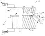
- FIG. 4is a schematic representation of a system 100 for depositing material onto a micro-device workpiece W in accordance with one embodiment of the invention.
- the system 100includes a reactor 110 having a reaction chamber 120 coupled to a gas supply 130 and a vacuum 140 .
- the reactor 110also includes a gas distributor 160 coupled to the gas supply 130 and a workpiece holder 150 that supports the workpiece W.
- the gas distributor 160is positioned over the workpiece holder 150 to deliver gas(es) to the workpiece W.
- the workpiece holder 150can be a heater or heat sink that holds the workpiece W at a desired temperature. In other embodiments, however, the workpiece holder 150 may not be heated.
- the reaction chamber 120is coupled to the vacuum 140 to draw gases from the gas distributor 160 across the workpiece W and then out of the reaction chamber 120 .
- the system 100further includes an access chamber 169 that includes a passageway 170 configured to provide ingression to and egression from the reaction chamber 120 for the workpiece W.
- the passageway 170includes a first end 171 open to the reaction chamber 120 and a second end 172 apart from the first end 171 .
- a robotic devicecan pass a workpiece W through the passageway 170 and place the workpiece on the workpiece holder 150 . After processing, the robotic device removes the workpiece W from the workpiece holder 150 and carries the workpiece back through the passageway 170 .
- the system 100further includes a door assembly 175 located at the second end 172 of the passageway 170 .
- the door assembly 175includes a door 176 and an actuator assembly 180 to move the door 176 between a first position to open the passageway 172 and a second position to close the passageway 172 .
- the actuator assembly 180includes an actuator shaft 181 , an actuator 182 that receives a portion of the actuator shaft 181 , a first fluid inlet/outlet 183 , and a second fluid inlet/outlet 184 .
- the actuator assembly 180can further include a bellows 185 that surrounds a portion of the shaft 181 .
- One end of the shaft 181carries the door 176 , and the other end of the shaft 181 includes a piston head in the actuator 182 .
- pressurized airis injected into the first fluid inlet/outlet 183 while exhaust air flows through the second inlet/outlet 184 to disengage the door 176 from the second end 172 of the passageway 170 .
- pressurized airis injected through the second fluid inlet/outlet 184 while exhaust air flows through the first inlet/outlet 183 to engage the door 176 with the second end 172 of the passageway 170 .
- the door 176seals the passageway 170 in the closed or second position for processing the workpiece W in the reaction chamber 120 .
- the system 100further includes a gas conditioning system 190 at least proximate to the second end 172 of the passageway 170 .
- the gas conditioning system 190can be a component carried by the door 176 and/or the access chamber 169 at the second end 172 of the passageway 170 .
- the gas conditioning system 190is configured to maintain or control the desired concentration and/or phase of the reactive constituents within the passageway 170 .
- several embodiments of the gas conditioning system 190are expected to mitigate or inhibit adsorption and/or desorption of constituent gases within the passageway that can reduce the quality of the film deposited on the workpiece W.
- gas conditioning systems 190are described in more detail below with reference to FIGS. 5-10 .
- FIG. 5is a cross-sectional view of an embodiment of a gas conditioning system 190 in accordance with an embodiment of the invention.
- the gas conditioning system 190includes a secondary gas passage 202 in the door 176 and the actuator shaft 181 .
- the gas conditioning system 190also includes a plate 204 attached to the door 176 .
- the plate 204includes a plurality of flow ports 206 .
- a seal 208can extend around the plate 204 to seal the door 176 to the second end 172 of the passageway 170 . In operation, the door 176 is sealed to the second end of the passageway, and then a secondary gas flows through the secondary gas passage 202 and the flow ports 206 .
- the flow ports 206can be configured to project the secondary gas flow along a vector parallel to the passageway 170 . In other embodiments, the flow ports 206 can be configured to direct the flow of the secondary gas along a different vector at an angle to the passageway 170 or to create a vortex within the passageway 170 .
- the secondary gas flowing through the flow ports 206can be a purge gas.
- the purge gascan be the same gas that is used during the purge cycle for ALD or CVD processing.
- the secondary gascan be a different type of purge gas.
- the secondary gascan flow continuously during a deposition cycle, or it can flow for only a portion of the deposition cycle.
- a secondary gascan flow only during the purge cycle in certain embodiments, or it can flow during the pulses of one or more precursor gases in addition to or in lieu of flowing during the purge cycle.
- the secondary gascan flow periodically or continuously during a deposition cycle or between deposition cycles.
- One advantage of the embodiment illustrated in FIG. 5is that the flow of secondary gas in the passageway 170 inhibits adsorption and/or desorption of the precursor gases in the passageway 170 .
- the present inventorshave discovered that the precursors are particularly susceptible to adsorp to the access chamber because the passageway 170 can entrap some of the precursor molecules and it may not be at the same temperature as the reaction chamber 120 .
- the flow of secondary gasis expected to “scrub” or remove precursors from the passageway before they can adsorp to the surface of the door 176 or the access chamber 169 .
- the flow of secondary gas through the passageway 170therefore, should provide better control of the concentration and phase of precursors in the reaction chamber that will result in higher quality films.
- FIG. 6is a cross-sectional view illustrating another embodiment of the gas conditioning system 190 in accordance with the invention.
- the gas conditioning system 190includes a temperature control system 320 carried by the door 176 .
- the temperature control system 320can be an electrical element, a fluid passageway for a heated fluid, an infrared element, or another type of device for maintaining a desired temperature at the second end 172 of the passageway 170 .
- the temperature control system 320can further include leads or fluid lines 322 that run through the shaft 181 .
- the temperature control system 320typically heats the door 176 to maintain a temperature at the second end 172 of the passageway 170 at which the precursor gases do not adsorp to the walls of the passageway 170 or the door 176 .
- One advantage of the particular embodiment of the gas conditioning system 190 shown in FIG. 6is that by precisely controlling the temperature at the second end 172 of the passageway 170 , adsorption and/or desorption of gases in the passageway 170 is reduced in a manner that is expected to provide higher quality films on workpieces.
- FIG. 7illustrates another embodiment of the gas conditioning system 190 including the secondary gas passage 202 , the plate 204 with the flow ports 206 , and the temperature control system 320 in the door 176 .
- the flow ports 206 and the temperature control system 320can be similar to the components described above with reference to FIGS. 5 and 6 . In the embodiment shown in FIG. 7 , however, these two features operate together to maintain a desired concentration and phase of gas constituents in the passageway 170 . As with the embodiments show in FIGS. 5 and 6 , this embodiment is expected to (a) mitigate contamination of the workpiece W ( FIG. 4 ) as it passes through the passageway 170 and (b) enhance the quality of the film deposited on the workpiece.
- FIGS. 8-10are cross-sectional views illustrating additional embodiments of reactors with gas conditioning systems. Like reference numbers refer to like components in FIGS. 5-7 and 8 - 10 , and thus specific details of components described above are not repeated.
- FIG. 8is a cross-sectional view of a gas conditioning system 800 including a plurality of flow ports 810 in the wall of the passageway 170 and a secondary gas passage 812 .
- a secondary gaspasses through the secondary gas passage 812 and flows through the flow ports 810 into the second end 172 of the passageway 170 .
- FIG. 9is a cross-sectional view of another embodiment of a gas conditioning system 900 including a temperature control system 920 in or at the wall of the passageway 170 rather than the door 176 .
- the temperature control system 920is a heating element positioned in the wall of the passageway 170 near the second end 172 of the passageway 170 .
- the temperature control system 920can be an electrical or fluid system that has leads or fluid lines 922 .
- FIG. 10is a cross-sectional view of a gas control system 1000 that includes a temperature control system 920 and flow ports 810 in or at the wall near the second end 172 of the passageway 170 .
- the flow ports 810 and temperature control system 920 of this embodimentcan operate as described above with reference to embodiments shown in FIGS. 8 and 9 .
- the gas conditioning systemcan have one heating element or a set of flow ports in the door and/or another heating element or another set of flow ports in the wall at the second end of the passageway. Accordingly, the invention is not limited except as by the appended claims.
Landscapes
- Chemical & Material Sciences (AREA)
- General Chemical & Material Sciences (AREA)
- Chemical Kinetics & Catalysis (AREA)
- Engineering & Computer Science (AREA)
- Materials Engineering (AREA)
- Mechanical Engineering (AREA)
- Metallurgy (AREA)
- Organic Chemistry (AREA)
- Chemical Vapour Deposition (AREA)
Abstract
Description
Claims (23)
Priority Applications (1)
| Application Number | Priority Date | Filing Date | Title |
|---|---|---|---|
| US10/932,470US7427425B2 (en) | 2003-02-11 | 2004-09-01 | Reactors with isolated gas connectors and methods for depositing materials onto micro-device workpieces |
Applications Claiming Priority (2)
| Application Number | Priority Date | Filing Date | Title |
|---|---|---|---|
| US10/365,085US6926775B2 (en) | 2003-02-11 | 2003-02-11 | Reactors with isolated gas connectors and methods for depositing materials onto micro-device workpieces |
| US10/932,470US7427425B2 (en) | 2003-02-11 | 2004-09-01 | Reactors with isolated gas connectors and methods for depositing materials onto micro-device workpieces |
Related Parent Applications (1)
| Application Number | Title | Priority Date | Filing Date |
|---|---|---|---|
| US10/365,085DivisionUS6926775B2 (en) | 2003-02-11 | 2003-02-11 | Reactors with isolated gas connectors and methods for depositing materials onto micro-device workpieces |
Publications (2)
| Publication Number | Publication Date |
|---|---|
| US20050028734A1 US20050028734A1 (en) | 2005-02-10 |
| US7427425B2true US7427425B2 (en) | 2008-09-23 |
Family
ID=32824554
Family Applications (2)
| Application Number | Title | Priority Date | Filing Date |
|---|---|---|---|
| US10/365,085Expired - Fee RelatedUS6926775B2 (en) | 2003-02-11 | 2003-02-11 | Reactors with isolated gas connectors and methods for depositing materials onto micro-device workpieces |
| US10/932,470Expired - LifetimeUS7427425B2 (en) | 2003-02-11 | 2004-09-01 | Reactors with isolated gas connectors and methods for depositing materials onto micro-device workpieces |
Family Applications Before (1)
| Application Number | Title | Priority Date | Filing Date |
|---|---|---|---|
| US10/365,085Expired - Fee RelatedUS6926775B2 (en) | 2003-02-11 | 2003-02-11 | Reactors with isolated gas connectors and methods for depositing materials onto micro-device workpieces |
Country Status (1)
| Country | Link |
|---|---|
| US (2) | US6926775B2 (en) |
Cited By (2)
| Publication number | Priority date | Publication date | Assignee | Title |
|---|---|---|---|---|
| US20100084398A1 (en)* | 2008-10-02 | 2010-04-08 | Applied Materials, Inc. | Balanced purge slit valve |
| US9695510B2 (en) | 2011-04-21 | 2017-07-04 | Kurt J. Lesker Company | Atomic layer deposition apparatus and process |
Families Citing this family (40)
| Publication number | Priority date | Publication date | Assignee | Title |
|---|---|---|---|---|
| US7485134B2 (en)* | 2001-12-07 | 2009-02-03 | Simonson Rush E | Vertebral implants adapted for posterior insertion |
| US6670071B2 (en)* | 2002-01-15 | 2003-12-30 | Quallion Llc | Electric storage battery construction and method of manufacture |
| US6800172B2 (en)* | 2002-02-22 | 2004-10-05 | Micron Technology, Inc. | Interfacial structure for semiconductor substrate processing chambers and substrate transfer chambers and for semiconductor substrate processing chambers and accessory attachments, and semiconductor substrate processor |
| US6814813B2 (en)* | 2002-04-24 | 2004-11-09 | Micron Technology, Inc. | Chemical vapor deposition apparatus |
| US6858264B2 (en)* | 2002-04-24 | 2005-02-22 | Micron Technology, Inc. | Chemical vapor deposition methods |
| US6838114B2 (en) | 2002-05-24 | 2005-01-04 | Micron Technology, Inc. | Methods for controlling gas pulsing in processes for depositing materials onto micro-device workpieces |
| US6821347B2 (en) | 2002-07-08 | 2004-11-23 | Micron Technology, Inc. | Apparatus and method for depositing materials onto microelectronic workpieces |
| US6955725B2 (en) | 2002-08-15 | 2005-10-18 | Micron Technology, Inc. | Reactors with isolated gas connectors and methods for depositing materials onto micro-device workpieces |
| US6926775B2 (en) | 2003-02-11 | 2005-08-09 | Micron Technology, Inc. | Reactors with isolated gas connectors and methods for depositing materials onto micro-device workpieces |
| US7335396B2 (en) | 2003-04-24 | 2008-02-26 | Micron Technology, Inc. | Methods for controlling mass flow rates and pressures in passageways coupled to reaction chambers and systems for depositing material onto microfeature workpieces in reaction chambers |
| US7235138B2 (en) | 2003-08-21 | 2007-06-26 | Micron Technology, Inc. | Microfeature workpiece processing apparatus and methods for batch deposition of materials on microfeature workpieces |
| US7344755B2 (en) | 2003-08-21 | 2008-03-18 | Micron Technology, Inc. | Methods and apparatus for processing microfeature workpieces; methods for conditioning ALD reaction chambers |
| US7422635B2 (en)* | 2003-08-28 | 2008-09-09 | Micron Technology, Inc. | Methods and apparatus for processing microfeature workpieces, e.g., for depositing materials on microfeature workpieces |
| US7056806B2 (en) | 2003-09-17 | 2006-06-06 | Micron Technology, Inc. | Microfeature workpiece processing apparatus and methods for controlling deposition of materials on microfeature workpieces |
| US7282239B2 (en) | 2003-09-18 | 2007-10-16 | Micron Technology, Inc. | Systems and methods for depositing material onto microfeature workpieces in reaction chambers |
| KR20050033216A (en)* | 2003-10-06 | 2005-04-12 | 동부아남반도체 주식회사 | High density plasma device |
| US7323231B2 (en) | 2003-10-09 | 2008-01-29 | Micron Technology, Inc. | Apparatus and methods for plasma vapor deposition processes |
| US7581511B2 (en) | 2003-10-10 | 2009-09-01 | Micron Technology, Inc. | Apparatus and methods for manufacturing microfeatures on workpieces using plasma vapor processes |
| US7647886B2 (en) | 2003-10-15 | 2010-01-19 | Micron Technology, Inc. | Systems for depositing material onto workpieces in reaction chambers and methods for removing byproducts from reaction chambers |
| US7258892B2 (en) | 2003-12-10 | 2007-08-21 | Micron Technology, Inc. | Methods and systems for controlling temperature during microfeature workpiece processing, e.g., CVD deposition |
| US7906393B2 (en) | 2004-01-28 | 2011-03-15 | Micron Technology, Inc. | Methods for forming small-scale capacitor structures |
| US7584942B2 (en) | 2004-03-31 | 2009-09-08 | Micron Technology, Inc. | Ampoules for producing a reaction gas and systems for depositing materials onto microfeature workpieces in reaction chambers |
| US20050249873A1 (en)* | 2004-05-05 | 2005-11-10 | Demetrius Sarigiannis | Apparatuses and methods for producing chemically reactive vapors used in manufacturing microelectronic devices |
| US8133554B2 (en) | 2004-05-06 | 2012-03-13 | Micron Technology, Inc. | Methods for depositing material onto microfeature workpieces in reaction chambers and systems for depositing materials onto microfeature workpieces |
| US7699932B2 (en) | 2004-06-02 | 2010-04-20 | Micron Technology, Inc. | Reactors, systems and methods for depositing thin films onto microfeature workpieces |
| US20060165873A1 (en)* | 2005-01-25 | 2006-07-27 | Micron Technology, Inc. | Plasma detection and associated systems and methods for controlling microfeature workpiece deposition processes |
| US20060237138A1 (en)* | 2005-04-26 | 2006-10-26 | Micron Technology, Inc. | Apparatuses and methods for supporting microelectronic devices during plasma-based fabrication processes |
| SG174771A1 (en)* | 2006-06-09 | 2011-10-28 | Soitec Silicon On Insulator | High volume delivery system for gallium trichloride |
| US9481944B2 (en) | 2006-11-22 | 2016-11-01 | Soitec | Gas injectors including a funnel- or wedge-shaped channel for chemical vapor deposition (CVD) systems and CVD systems with the same |
| WO2008064080A1 (en)* | 2006-11-22 | 2008-05-29 | S.O.I.Tec Silicon On Insulator Technologies | High volume delivery system for gallium trichloride |
| US8382898B2 (en) | 2006-11-22 | 2013-02-26 | Soitec | Methods for high volume manufacture of group III-V semiconductor materials |
| US9481943B2 (en) | 2006-11-22 | 2016-11-01 | Soitec | Gallium trichloride injection scheme |
| US8197597B2 (en) | 2006-11-22 | 2012-06-12 | Soitec | Gallium trichloride injection scheme |
| JP5575483B2 (en)* | 2006-11-22 | 2014-08-20 | ソイテック | Mass production equipment for III-V semiconductor materials |
| JP5244814B2 (en) | 2006-11-22 | 2013-07-24 | ソイテック | Method, assembly and system using temperature controlled purge gate valve for chemical vapor deposition chamber |
| US8377213B2 (en) | 2008-05-05 | 2013-02-19 | Applied Materials, Inc. | Slit valve having increased flow uniformity |
| JP5356732B2 (en)* | 2008-06-06 | 2013-12-04 | 株式会社日立ハイテクノロジーズ | Vacuum processing equipment |
| US20120112026A1 (en)* | 2010-11-10 | 2012-05-10 | Kimball Physics, Inc. | Apparatus for supporting an assembly of conflat-connected ultra-high vacuum modules |
| US20180240684A1 (en)* | 2015-09-30 | 2018-08-23 | Tokyo Electron Limited | Substrate processing apparatus and substrate processing method |
| KR102239116B1 (en)* | 2019-08-07 | 2021-04-09 | 세메스 주식회사 | Apparatus for processing substrate |
Citations (221)
| Publication number | Priority date | Publication date | Assignee | Title |
|---|---|---|---|---|
| US2508500A (en) | 1942-05-23 | 1950-05-23 | Hartford Nat Bank & Trust Co | Apparatus for applying metal coatings on insulators |
| US3522836A (en) | 1966-07-06 | 1970-08-04 | Battelle Development Corp | Method of manufacturing wire and the like |
| US3618919A (en) | 1969-11-03 | 1971-11-09 | Btu Eng Corp | Adjustable heat and gas barrier |
| US4289061A (en) | 1977-10-03 | 1981-09-15 | Hooker Chemicals & Plastics Corp. | Device and assembly for mounting parts |
| US4313783A (en) | 1980-05-19 | 1982-02-02 | Branson International Plasma Corporation | Computer controlled system for processing semiconductor wafers |
| US4388342A (en) | 1979-05-29 | 1983-06-14 | Hitachi, Ltd. | Method for chemical vapor deposition |
| US4436674A (en) | 1981-07-30 | 1984-03-13 | J.C. Schumacher Co. | Vapor mass flow control system |
| US4438724A (en) | 1982-08-13 | 1984-03-27 | Energy Conversion Devices, Inc. | Grooved gas gate |
| US4509456A (en) | 1981-07-28 | 1985-04-09 | Veb Zentrum Fur Forschung Und Technologie Mikroelektronik | Apparatus for guiding gas for LP CVD processes in a tube reactor |
| US4545136A (en) | 1981-03-16 | 1985-10-08 | Sovonics Solar Systems | Isolation valve |
| US4593644A (en) | 1983-10-26 | 1986-06-10 | Rca Corporation | Continuous in-line deposition system |
| JPS62235728A (en) | 1986-04-07 | 1987-10-15 | Nec Corp | Vapor phase epitaxial growth device |
| JPS62263629A (en) | 1986-05-12 | 1987-11-16 | Hitachi Ltd | Vapor phase growth equipment |
| US4738295A (en) | 1985-04-02 | 1988-04-19 | Genser Hans G | Method and apparatus for evaporating a fluid in a rotating vacuum evaporation system |
| JPS6320490Y2 (en) | 1979-09-08 | 1988-06-07 | ||
| JPS63111177U (en) | 1987-01-12 | 1988-07-16 | ||
| JPS63234198A (en) | 1987-03-24 | 1988-09-29 | 株式会社東芝 | Flange image leakage detection device |
| JPS63256460A (en) | 1987-04-14 | 1988-10-24 | Oki Electric Ind Co Ltd | Substrate for thermal head and production thereof |
| US4780178A (en) | 1982-10-15 | 1988-10-25 | Yamoto Scientific Co. Ltd. | Rotary evaporator with control system |
| US4832115A (en) | 1986-07-09 | 1989-05-23 | Albers Technologies Corporation | Method and apparatus for simultaneous heat and mass transfer |
| US4871417A (en) | 1986-07-04 | 1989-10-03 | Dainippon Screen Mfg. Co., Ltd. | Method and apparatus for surface treating of substrates |
| JPH01273991A (en) | 1988-04-26 | 1989-11-01 | Ishikawajima Harima Heavy Ind Co Ltd | Furnace sealing device |
| US4894132A (en) | 1987-10-21 | 1990-01-16 | Mitsubishi Denki Kabushiki Kaisha | Sputtering method and apparatus |
| US4911638A (en) | 1989-05-18 | 1990-03-27 | Direction Incorporated | Controlled diffusion environment capsule and system |
| US4923715A (en) | 1986-03-31 | 1990-05-08 | Kabushiki Kaisha Toshiba | Method of forming thin film by chemical vapor deposition |
| US4948979A (en) | 1987-12-21 | 1990-08-14 | Kabushiki Kaisha Toshiba | Vacuum device for handling workpieces |
| US4949669A (en) | 1988-12-20 | 1990-08-21 | Texas Instruments Incorporated | Gas flow systems in CCVD reactors |
| US5015330A (en) | 1989-02-28 | 1991-05-14 | Kabushiki Kaisha Toshiba | Film forming method and film forming device |
| US5017404A (en) | 1988-09-06 | 1991-05-21 | Schott Glaswerke | Plasma CVD process using a plurality of overlapping plasma columns |
| US5020476A (en) | 1990-04-17 | 1991-06-04 | Ds Research, Inc. | Distributed source assembly |
| JPH03174717A (en) | 1989-10-06 | 1991-07-29 | Nippon Kentetsu Co Ltd | Method of supplying water of plasma ashing |
| US5062446A (en) | 1991-01-07 | 1991-11-05 | Sematech, Inc. | Intelligent mass flow controller |
| US5076205A (en) | 1989-01-06 | 1991-12-31 | General Signal Corporation | Modular vapor processor system |
| US5090985A (en) | 1989-10-17 | 1992-02-25 | Libbey-Owens-Ford Co. | Method for preparing vaporized reactants for chemical vapor deposition |
| JPH04100533A (en) | 1990-08-18 | 1992-04-02 | Mitsubishi Electric Corp | vacuum container |
| US5172849A (en) | 1991-09-25 | 1992-12-22 | General Motors Corporation | Method and apparatus for convection brazing of aluminum heat exchangers |
| US5223113A (en) | 1990-07-20 | 1993-06-29 | Tokyo Electron Limited | Apparatus for forming reduced pressure and for processing object |
| US5286296A (en)* | 1991-01-10 | 1994-02-15 | Sony Corporation | Multi-chamber wafer process equipment having plural, physically communicating transfer means |
| JPH06151558A (en) | 1992-11-09 | 1994-05-31 | Tokyo Electron Ltd | Transfer processing device |
| US5325020A (en) | 1990-09-28 | 1994-06-28 | Abtox, Inc. | Circular waveguide plasma microwave sterilizer apparatus |
| JPH06201539A (en) | 1993-01-04 | 1994-07-19 | Yasuo Kitsuta | Centrifugal evaporator |
| JPH06202372A (en) | 1992-10-21 | 1994-07-22 | Hewlett Packard Co <Hp> | Toner composition and its adjusting method |
| US5364219A (en) | 1991-06-24 | 1994-11-15 | Tdk Corporation | Apparatus for clean transfer of objects |
| US5366557A (en) | 1990-06-18 | 1994-11-22 | At&T Bell Laboratories | Method and apparatus for forming integrated circuit layers |
| JPH06342785A (en) | 1993-06-01 | 1994-12-13 | Fujitsu Ltd | Exhauster of vapor growth device and cleaning method thereof |
| US5433787A (en) | 1991-12-12 | 1995-07-18 | Canon Kabushiki Kaisha | Apparatus for forming deposited film including light transmissive diffusion plate |
| US5445491A (en) | 1991-08-27 | 1995-08-29 | Toshiba Kikai Kabushiki Kaisha | Method for multichamber sheet-after-sheet type treatment |
| US5453124A (en) | 1992-12-30 | 1995-09-26 | Texas Instruments Incorporated | Programmable multizone gas injector for single-wafer semiconductor processing equipment |
| US5474612A (en) | 1990-03-19 | 1995-12-12 | Kabushiki Kaisha Toshiba | Vapor-phase deposition apparatus and vapor-phase deposition method |
| US5477623A (en) | 1992-11-25 | 1995-12-26 | Matsushita Electric Industrial Co., Ltd. | Drying apparatus |
| JPH0834678A (en) | 1994-07-27 | 1996-02-06 | Matsushita Electric Works Ltd | Aerogel panel |
| US5496410A (en) | 1992-03-10 | 1996-03-05 | Hitachi, Ltd. | Plasma processing apparatus and method of processing substrates by using same apparatus |
| US5498292A (en) | 1994-06-16 | 1996-03-12 | Kishimoto Sangyo Co., Ltd. | Heating device used for a gas phase growing mechanism or heat treatment mechanism |
| US5532190A (en) | 1994-05-26 | 1996-07-02 | U.S. Philips Corporation | Plasma treatment method in electronic device manufacture |
| US5536317A (en) | 1995-10-27 | 1996-07-16 | Specialty Coating Systems, Inc. | Parylene deposition apparatus including a quartz crystal thickness/rate controller |
| US5562800A (en) | 1993-09-20 | 1996-10-08 | Hitachi, Ltd. | Wafer transport method |
| US5575883A (en) | 1993-07-09 | 1996-11-19 | Fujitsu Limited | Apparatus and process for fabricating semiconductor devices |
| US5589110A (en) | 1992-11-20 | 1996-12-31 | Mitsubishi Electric Corp | Container for liquid metal organic compound |
| US5592581A (en) | 1993-07-19 | 1997-01-07 | Tokyo Electron Kabushiki Kaisha | Heat treatment apparatus |
| JPH0982650A (en) | 1995-09-14 | 1997-03-28 | Kokusai Electric Co Ltd | Semiconductor manufacturing equipment |
| US5626936A (en) | 1993-09-09 | 1997-05-06 | Energy Pillow, Inc. | Phase change insulation system |
| US5640751A (en) | 1995-07-17 | 1997-06-24 | Thermionics Laboratories, Inc. | Vacuum flange |
| US5683538A (en) | 1994-12-23 | 1997-11-04 | International Business Machines Corporation | Control of etch selectivity |
| US5693288A (en) | 1994-06-24 | 1997-12-02 | Nisshin Steel Co., Ltd. | Seal assembly for thermal treatment furnaces using an atmospheric gas containing hydrogen gas |
| JPH108255A (en) | 1996-06-20 | 1998-01-13 | Ebara Corp | Liquid raw material vaporizing device |
| US5716796A (en) | 1990-01-23 | 1998-02-10 | Medical Devices Corporation | Optical blood hemostatic analysis apparatus and method |
| US5733375A (en) | 1995-01-06 | 1998-03-31 | Tokyo Electron Limited | Apparatus for supplying a treatment material |
| US5746434A (en) | 1996-07-09 | 1998-05-05 | Lam Research Corporation | Chamber interfacing O-rings and method for implementing same |
| US5754297A (en) | 1994-01-28 | 1998-05-19 | Applied Materials, Inc. | Method and apparatus for monitoring the deposition rate of films during physical vapor deposition |
| US5766364A (en) | 1996-07-17 | 1998-06-16 | Matsushita Electric Industrial Co., Ltd. | Plasma processing apparatus |
| US5769950A (en) | 1985-07-23 | 1998-06-23 | Canon Kabushiki Kaisha | Device for forming deposited film |
| US5769952A (en) | 1994-06-07 | 1998-06-23 | Tokyo Electron, Ltd. | Reduced pressure and normal pressure treatment apparatus |
| US5772771A (en) | 1995-12-13 | 1998-06-30 | Applied Materials, Inc. | Deposition chamber for improved deposition thickness uniformity |
| JPH10223419A (en) | 1997-02-05 | 1998-08-21 | Sony Corp | Magnetic substance and manufacture thereof |
| US5803938A (en) | 1992-09-21 | 1998-09-08 | Mitsubishi Denki Kabushiki Kaisha | Liquid vaporizing apparatus |
| US5820641A (en) | 1996-02-09 | 1998-10-13 | Mks Instruments, Inc. | Fluid cooled trap |
| US5820686A (en) | 1993-01-21 | 1998-10-13 | Moore Epitaxial, Inc. | Multi-layer susceptor for rapid thermal process reactors |
| US5819683A (en) | 1995-05-02 | 1998-10-13 | Tokyo Electron Limited | Trap apparatus |
| US5827370A (en) | 1997-01-13 | 1998-10-27 | Mks Instruments, Inc. | Method and apparatus for reducing build-up of material on inner surface of tube downstream from a reaction furnace |
| US5851294A (en) | 1995-10-23 | 1998-12-22 | Watkins-Johnson Company | Gas injection system for semiconductor processing |
| US5866986A (en) | 1996-08-05 | 1999-02-02 | Integrated Electronic Innovations, Inc. | Microwave gas phase plasma source |
| US5868159A (en) | 1996-07-12 | 1999-02-09 | Mks Instruments, Inc. | Pressure-based mass flow controller |
| US5879516A (en) | 1996-02-29 | 1999-03-09 | Kasman; David H. | Kugelrohr or distillation apparatus |
| US5885425A (en) | 1995-06-06 | 1999-03-23 | International Business Machines Corporation | Method for selective material deposition on one side of raised or recessed features |
| US5902403A (en) | 1995-11-28 | 1999-05-11 | Applied Materials, Inc. | Method and apparatus for cleaning a chamber |
| US5911238A (en) | 1996-10-04 | 1999-06-15 | Emerson Electric Co. | Thermal mass flowmeter and mass flow controller, flowmetering system and method |
| US5936829A (en) | 1997-01-02 | 1999-08-10 | Cvc Products, Inc. | Thermally conductive chuck for vacuum processor |
| US5940684A (en) | 1996-05-23 | 1999-08-17 | Rohm, Co., Ltd. | Method and equipment for manufacturing semiconductor device |
| US5958140A (en) | 1995-07-27 | 1999-09-28 | Tokyo Electron Limited | One-by-one type heat-processing apparatus |
| US5963336A (en) | 1995-10-10 | 1999-10-05 | American Air Liquide Inc. | Chamber effluent monitoring system and semiconductor processing system comprising absorption spectroscopy measurement system, and methods of use |
| US5961775A (en) | 1987-08-19 | 1999-10-05 | Fujitsu Limited | Apparatus for removing organic resist from semiconductor |
| US5998932A (en) | 1998-06-26 | 1999-12-07 | Lam Research Corporation | Focus ring arrangement for substantially eliminating unconfined plasma in a plasma processing chamber |
| US5997588A (en) | 1995-10-13 | 1999-12-07 | Advanced Semiconductor Materials America, Inc. | Semiconductor processing system with gas curtain |
| US6006694A (en) | 1997-12-05 | 1999-12-28 | Tegal Corporation | Plasma reactor with a deposition shield |
| US6016611A (en) | 1998-07-13 | 2000-01-25 | Applied Komatsu Technology, Inc. | Gas flow control in a substrate processing system |
| US6022483A (en) | 1998-03-10 | 2000-02-08 | Intergrated Systems, Inc. | System and method for controlling pressure |
| US6039557A (en) | 1989-12-22 | 2000-03-21 | Imarx Pharmaceutical Corp. | Apparatus for making gas-filled vesicles of optimal size |
| US6045620A (en) | 1997-07-11 | 2000-04-04 | Applied Materials, Inc. | Two-piece slit valve insert for vacuum processing system |
| US6090210A (en) | 1996-07-24 | 2000-07-18 | Applied Materials, Inc. | Multi-zone gas flow control in a process chamber |
| US6089543A (en) | 1997-07-11 | 2000-07-18 | Applied Materials, Inc. | Two-piece slit valve door with molded-in-place seal for a vacuum processing system |
| US6113698A (en) | 1997-07-10 | 2000-09-05 | Applied Materials, Inc. | Degassing method and apparatus |
| US6142163A (en) | 1996-03-29 | 2000-11-07 | Lam Research Corporation | Method and apparatus for pressure control in vacuum processors |
| US6143078A (en) | 1998-11-13 | 2000-11-07 | Applied Materials, Inc. | Gas distribution system for a CVD processing chamber |
| US6159298A (en) | 1997-12-27 | 2000-12-12 | Tokyo Electron Limited | Thermal processing system |
| US6159297A (en) | 1996-04-25 | 2000-12-12 | Applied Materials, Inc. | Semiconductor process chamber and processing method |
| US6174366B1 (en) | 1993-12-23 | 2001-01-16 | Heikki Ihantola | Apparatus and method for processing of semiconductors, such as silicon chips |
| US6178660B1 (en) | 1999-08-03 | 2001-01-30 | International Business Machines Corporation | Pass-through semiconductor wafer processing tool and process for gas treating a moving semiconductor wafer |
| US6183563B1 (en) | 1998-05-18 | 2001-02-06 | Ips Ltd. | Apparatus for depositing thin films on semiconductor wafers |
| US6190459B1 (en) | 1998-01-07 | 2001-02-20 | Tokyo Electron Limited | Gas treatment apparatus |
| US6193802B1 (en) | 1995-09-25 | 2001-02-27 | Applied Materials, Inc. | Parallel plate apparatus for in-situ vacuum line cleaning for substrate processing equipment |
| US6194628B1 (en) | 1995-09-25 | 2001-02-27 | Applied Materials, Inc. | Method and apparatus for cleaning a vacuum line in a CVD system |
| US6192827B1 (en) | 1998-07-03 | 2001-02-27 | Applied Materials, Inc. | Double slit-valve doors for plasma processing |
| US6197119B1 (en) | 1999-02-18 | 2001-03-06 | Mks Instruments, Inc. | Method and apparatus for controlling polymerized teos build-up in vacuum pump lines |
| US6200415B1 (en) | 1999-06-30 | 2001-03-13 | Lam Research Corporation | Load controlled rapid assembly clamp ring |
| US6207937B1 (en) | 1998-05-11 | 2001-03-27 | Semitool, Inc. | Temperature control system for a thermal reactor |
| US6206967B1 (en) | 1997-12-02 | 2001-03-27 | Applied Materials, Inc. | Low resistivity W using B2H6 nucleation step |
| JP2001082682A (en) | 1999-09-10 | 2001-03-30 | Matsushita Refrig Co Ltd | Heat insulating material and heat insulating structure |
| WO2001032966A1 (en) | 1999-11-02 | 2001-05-10 | Zakrytoe Aktsionernoe Obschestvo 'pandzhsher-Kholding' | Method for producing an initial polycrystalline silicon in the form of plates having a large surface and chamber for the precipitation of silicon |
| US20010001952A1 (en) | 1984-07-26 | 2001-05-31 | Junichi Nishizawa | Semiconductor crystal growth apparatus |
| US6251190B1 (en) | 1997-06-30 | 2001-06-26 | Applied Materials, Inc. | Gate electrode connection structure by in situ chemical vapor deposition of tungsten and tungsten nitride |
| US6255222B1 (en) | 1999-08-24 | 2001-07-03 | Applied Materials, Inc. | Method for removing residue from substrate processing chamber exhaust line for silicon-oxygen-carbon deposition process |
| US6263829B1 (en) | 1999-01-22 | 2001-07-24 | Applied Materials, Inc. | Process chamber having improved gas distributor and method of manufacture |
| US6264788B1 (en) | 1994-04-20 | 2001-07-24 | Tokyo Electron Limited | Plasma treatment method and apparatus |
| US20010012697A1 (en) | 1996-04-03 | 2001-08-09 | Kabushiki Kaisha Toshiba | Apparatus for manufacturing a semiconductor device in a CVD reactive chamber |
| US6273954B2 (en) | 1998-09-03 | 2001-08-14 | Mitsubishi Denki Kabushiki Kaisha | System for manufacturing a semiconductor device |
| US6277763B1 (en) | 1999-12-16 | 2001-08-21 | Applied Materials, Inc. | Plasma processing of tungsten using a gas mixture comprising a fluorinated gas and oxygen |
| US6277757B1 (en) | 1999-06-01 | 2001-08-21 | Winbond Electronics Corp. | Methods to modify wet by dry etched via profile |
| US6280584B1 (en) | 1998-07-29 | 2001-08-28 | Applied Materials, Inc. | Compliant bond structure for joining ceramic to metal |
| US20010020447A1 (en) | 1997-04-02 | 2001-09-13 | Laxman Murugesh | Sequential in-situ heating and deposition of halogen-doped silicon oxide |
| US6294394B1 (en) | 1999-07-01 | 2001-09-25 | Voyan Technology | Ramp rate limiter to control stress during ramping |
| JP2001261375A (en) | 2000-03-14 | 2001-09-26 | Toshiba Ceramics Co Ltd | Ceramic coated quartz glass body |
| US6309161B1 (en) | 1999-11-04 | 2001-10-30 | Brooks Automation, Inc. | Load lock with vertically movable support |
| US6328803B2 (en) | 1997-02-21 | 2001-12-11 | Micron Technology, Inc. | Method and apparatus for controlling rate of pressure change in a vacuum process chamber |
| US20010050267A1 (en) | 1997-08-26 | 2001-12-13 | Hwang Jeng H. | Method for allowing a stable power transmission into a plasma processing chamber |
| US6333272B1 (en) | 2000-10-06 | 2001-12-25 | Lam Research Corporation | Gas distribution apparatus for semiconductor processing |
| US20010054484A1 (en) | 1999-11-22 | 2001-12-27 | Mitsuaki Komino | Plasma processor, cluster tool, and method of controlling plasma |
| US6334928B1 (en) | 1998-01-30 | 2002-01-01 | Kabushiki Kaisha Toshiba | Semiconductor processing system and method of using the same |
| US20020000202A1 (en) | 2000-06-29 | 2002-01-03 | Katsuhisa Yuda | Remote plasma apparatus for processing sustrate with two types of gases |
| US20020007790A1 (en)* | 2000-07-22 | 2002-01-24 | Park Young-Hoon | Atomic layer deposition (ALD) thin film deposition equipment having cleaning apparatus and cleaning method |
| US20020016044A1 (en) | 1997-02-20 | 2002-02-07 | Joerg Dreybrodt | Method of producing doped polysilicon layers and polysilicon layered structrues and method of structuring layers and layered structures which comprise polysilicon layers |
| US6347918B1 (en) | 1999-01-27 | 2002-02-19 | Applied Materials, Inc. | Inflatable slit/gate valve |
| US6364219B1 (en) | 1999-06-11 | 2002-04-02 | Larami Limited | Bladder water gun with shaped stream discharge orifices |
| US6383300B1 (en) | 1998-11-27 | 2002-05-07 | Tokyo Electron Ltd. | Heat treatment apparatus and cleaning method of the same |
| US6402849B2 (en) | 2000-03-17 | 2002-06-11 | Samsung Electronics Co., Ltd. | Process tube having slit type process gas injection portion and hole type waste gas exhaust portion, and apparatus for fabricating semiconductor device |
| US6402806B1 (en) | 1997-12-23 | 2002-06-11 | Applied Materials, Inc. | Method for unreacted precursor conversion and effluent removal |
| US6415736B1 (en) | 1999-06-30 | 2002-07-09 | Lam Research Corporation | Gas distribution apparatus for semiconductor processing |
| US6425168B1 (en) | 1994-09-30 | 2002-07-30 | Shin-Etsu Handotai Co., Ltd. | Quartz glass jig for heat-treating semiconductor wafers and method for producing same |
| US20020132374A1 (en) | 2001-02-02 | 2002-09-19 | Micron Technology, Inc. | Method for controlling deposition of dielectric films |
| US6486081B1 (en) | 1998-11-13 | 2002-11-26 | Applied Materials, Inc. | Gas distribution system for a CVD processing chamber |
| US20020185067A1 (en) | 2001-06-07 | 2002-12-12 | International Business Machines Corporation | Apparatus and method for in-situ cleaning of a throttle valve in a CVD system |
| US20020195201A1 (en) | 2001-06-25 | 2002-12-26 | Emanuel Beer | Apparatus and method for thermally isolating a heat chamber |
| US20020195145A1 (en) | 2001-04-13 | 2002-12-26 | Lowery Patrick A. | Mass flow meter systems and methods |
| US6506254B1 (en) | 2000-06-30 | 2003-01-14 | Lam Research Corporation | Semiconductor processing equipment having improved particle performance |
| US6508268B1 (en) | 1998-11-13 | 2003-01-21 | Ckd Corporation | Vacuum pressure control apparatus |
| US20030031794A1 (en) | 1997-12-24 | 2003-02-13 | Kunihiro Tada | Method of forming titanium film by CVD |
| US20030049372A1 (en) | 1997-08-11 | 2003-03-13 | Cook Robert C. | High rate deposition at low pressures in a small batch reactor |
| US6541353B1 (en) | 2000-08-31 | 2003-04-01 | Micron Technology, Inc. | Atomic layer doping apparatus and method |
| US6551929B1 (en) | 2000-06-28 | 2003-04-22 | Applied Materials, Inc. | Bifurcated deposition process for depositing refractory metal layers employing atomic layer deposition and chemical vapor deposition techniques |
| US6562141B2 (en) | 2000-07-03 | 2003-05-13 | Andrew Peter Clarke | Dual degas/cool loadlock cluster tool |
| US20030094903A1 (en) | 2001-11-20 | 2003-05-22 | Taiwan Semiconductor Manufacturing Co., Ltd | Selectively controllable gas feed zones for a plasma reactor |
| US20030098372A1 (en) | 2001-11-23 | 2003-05-29 | Jusung Engineering Co. | Multi-sectored flat board type showerhead used in CVD apparatus |
| US6580174B2 (en) | 2001-09-28 | 2003-06-17 | Intel Corporation | Vented vias for via in pad technology yield improvements |
| US6585823B1 (en) | 2000-07-07 | 2003-07-01 | Asm International, N.V. | Atomic layer deposition |
| US6593644B2 (en) | 2001-04-19 | 2003-07-15 | International Business Machines Corporation | System of a package fabricated on a semiconductor or dielectric wafer with wiring on one face, vias extending through the wafer, and external connections on the opposing face |
| US6602346B1 (en) | 2000-08-22 | 2003-08-05 | Novellus Systems, Inc. | Gas-purged vacuum valve |
| US6622104B2 (en) | 2000-07-24 | 2003-09-16 | Tokyo Electron Limited | Heat treatment apparatus, calibration method for temperature measuring system of the apparatus, and heat treatment system |
| US20030185979A1 (en) | 2002-03-29 | 2003-10-02 | Nelson Douglas M. | Method and apparatus for preparing vaporized reactants for chemical vapor deposition |
| US6638672B2 (en) | 2000-06-01 | 2003-10-28 | Canon Kabushiki Kaisha | Exposure apparatus, coating/developing apparatus, method of transferring a substrate, method of producing a device, semiconductor production factory, and method of maintaining an exposure apparatus |
| US20030213435A1 (en) | 2002-04-11 | 2003-11-20 | Kazuyuki Okuda | Vertical type semiconductor device producing apparatus |
| US6663713B1 (en) | 1996-01-08 | 2003-12-16 | Applied Materials Inc. | Method and apparatus for forming a thin polymer layer on an integrated circuit structure |
| US20030232892A1 (en) | 2002-06-18 | 2003-12-18 | Guerra-Santos Luis H. | Microcrystalline zeaxanthin with high bioavailability in oily carrier formulations |
| US6666982B2 (en) | 2001-10-22 | 2003-12-23 | Tokyo Electron Limited | Protection of dielectric window in inductively coupled plasma generation |
| US20040000270A1 (en) | 2002-06-26 | 2004-01-01 | Carpenter Craig M. | Methods and apparatus for vapor processing of micro-device workpieces |
| US6673196B1 (en) | 1999-09-02 | 2004-01-06 | Tokyo Electron Limited | Plasma processing apparatus |
| US6689220B1 (en) | 2000-11-22 | 2004-02-10 | Simplus Systems Corporation | Plasma enhanced pulsed layer deposition |
| US20040025786A1 (en) | 2002-04-05 | 2004-02-12 | Tadashi Kontani | Substrate processing apparatus and reaction container |
| US20040089240A1 (en) | 2002-04-24 | 2004-05-13 | Dando Ross S. | Chemical vapor deposition apparatus |
| US20040094095A1 (en) | 2002-11-19 | 2004-05-20 | Taiwan Semiconductor Manufacturing Co., Ltd. | Substrate holder assembly |
| US6770145B2 (en) | 2000-12-11 | 2004-08-03 | Tanaka Kikinzoku Kogyo K.K. | Low-pressure CVD apparatus and method of manufacturing a thin film |
| US20040154538A1 (en) | 2003-02-11 | 2004-08-12 | Carpenter Craig M. | Reactors with isolated gas connectors and methods for depositing materials onto micro-device workpieces |
| US6787463B2 (en) | 2002-04-11 | 2004-09-07 | Micron Technology, Inc. | Chemical vapor deposition methods, and atomic layer deposition method |
| US6800139B1 (en) | 1999-08-31 | 2004-10-05 | Tokyo Electron Limited | Film deposition apparatus and method |
| US6800172B2 (en) | 2002-02-22 | 2004-10-05 | Micron Technology, Inc. | Interfacial structure for semiconductor substrate processing chambers and substrate transfer chambers and for semiconductor substrate processing chambers and accessory attachments, and semiconductor substrate processor |
| US20040226516A1 (en) | 2003-05-13 | 2004-11-18 | Daniel Timothy J. | Wafer pedestal cover |
| US20040238123A1 (en) | 2003-05-22 | 2004-12-02 | Axcelis Technologies, Inc. | Plasma apparatus, gas distribution assembly for a plasma apparatus and processes therewith |
| US6828218B2 (en) | 2001-05-31 | 2004-12-07 | Samsung Electronics Co., Ltd. | Method of forming a thin film using atomic layer deposition |
| US6830652B1 (en) | 1999-05-26 | 2004-12-14 | Tokyo Electron Limited | Microwave plasma processing apparatus |
| US6838114B2 (en) | 2002-05-24 | 2005-01-04 | Micron Technology, Inc. | Methods for controlling gas pulsing in processes for depositing materials onto micro-device workpieces |
| US6845734B2 (en) | 2002-04-11 | 2005-01-25 | Micron Technology, Inc. | Deposition apparatuses configured for utilizing phased microwave radiation |
| US20050016956A1 (en) | 2003-03-14 | 2005-01-27 | Xinye Liu | Methods and apparatus for cycle time improvements for atomic layer deposition |
| US6849131B2 (en) | 2002-10-05 | 2005-02-01 | Taiwan Semiconductor Manufacturing Co., Ltd | Truncated dummy plate for process furnace |
| US6858264B2 (en) | 2002-04-24 | 2005-02-22 | Micron Technology, Inc. | Chemical vapor deposition methods |
| US6861356B2 (en) | 1997-11-05 | 2005-03-01 | Tokyo Electron Limited | Method of forming a barrier film and method of forming wiring structure and electrodes of semiconductor device having a barrier film |
| US20050048742A1 (en) | 2003-08-26 | 2005-03-03 | Tokyo Electron Limited | Multiple grow-etch cyclic surface treatment for substrate preparation |
| US20050045102A1 (en) | 2003-08-28 | 2005-03-03 | Zheng Lingyi A. | Methods and apparatus for processing microfeature workpieces, e.g., for depositing materials on microfeature workpieces |
| US20050061243A1 (en) | 2003-09-18 | 2005-03-24 | Demetrius Sarigiannis | Systems and methods for depositing material onto microfeature workpieces in reaction chambers |
| US6881295B2 (en) | 2000-03-28 | 2005-04-19 | Nec Electronics Corporation | Air-tight vessel equipped with gas feeder uniformly supplying gaseous component around plural wafers |
| US20050081786A1 (en) | 2003-10-15 | 2005-04-21 | Kubista David J. | Systems for depositing material onto workpieces in reaction chambers and methods for removing byproducts from reaction chambers |
| US20050087132A1 (en) | 2001-01-31 | 2005-04-28 | Planar Systems, Inc. | Methods and apparatus for the production of optical filters |
| US20050087302A1 (en) | 2003-10-10 | 2005-04-28 | Mardian Allen P. | Apparatus and methods for manufacturing microfeatures on workpieces using plasma vapor processes |
| US20050087130A1 (en) | 2003-10-09 | 2005-04-28 | Derderian Garo J. | Apparatus and methods for plasma vapor deposition processes |
| US6887521B2 (en) | 2002-08-15 | 2005-05-03 | Micron Technology, Inc. | Gas delivery system for pulsed-type deposition processes used in the manufacturing of micro-devices |
| US6905547B1 (en) | 2000-12-21 | 2005-06-14 | Genus, Inc. | Method and apparatus for flexible atomic layer deposition |
| US20050126489A1 (en) | 2003-12-10 | 2005-06-16 | Beaman Kevin L. | Methods and systems for controlling temperature during microfeature workpiece processing, e.g., CVD deposition |
| US20050133161A1 (en) | 2002-07-08 | 2005-06-23 | Carpenter Craig M. | Apparatus and method for depositing materials onto microelectronic workpieces |
| US20050145337A1 (en) | 2002-04-25 | 2005-07-07 | Derderian Garo J. | Apparatus for forming thin layers of materials on micro-device workpieces |
| US20050164466A1 (en) | 2004-01-28 | 2005-07-28 | Zheng Lingyi A. | Methods for forming small-scale capacitor structures |
| US20050217582A1 (en) | 2001-03-19 | 2005-10-06 | Apex Co., Ltd. | Chemical vapor deposition method |
| US20050217575A1 (en) | 2004-03-31 | 2005-10-06 | Dan Gealy | Ampoules for producing a reaction gas and systems for depositing materials onto microfeature workpieces in reaction chambers |
| US20050249887A1 (en) | 2004-05-06 | 2005-11-10 | Dando Ross S | Methods for depositing material onto microfeature workpieces in reaction chambers and systems for depositing materials onto microfeature workpieces |
| US20050249873A1 (en) | 2004-05-05 | 2005-11-10 | Demetrius Sarigiannis | Apparatuses and methods for producing chemically reactive vapors used in manufacturing microelectronic devices |
| US6966936B2 (en) | 1999-03-11 | 2005-11-22 | Tokyo Electron Limited | Processing system, evacuating system for processing system, low-pressure CVD system, and evacuating system and trapping device for low-pressure CVD system |
| US20050268856A1 (en) | 2004-06-02 | 2005-12-08 | Miller Matthew W | Reactors, systems and methods for depositing thin films onto microfeature workpieces |
| US6991684B2 (en) | 2000-09-29 | 2006-01-31 | Tokyo Electron Limited | Heat-treating apparatus and heat-treating method |
| US20060115957A1 (en) | 2003-09-17 | 2006-06-01 | Cem Basceri | Microfeature workpiece processing apparatus and methods for controlling deposition of materials on microfeature workpieces |
| US20060134345A1 (en) | 2004-12-20 | 2006-06-22 | Micron Technology, Inc. | Systems and methods for depositing material onto microfeature workpieces |
| US20060165873A1 (en) | 2005-01-25 | 2006-07-27 | Micron Technology, Inc. | Plasma detection and associated systems and methods for controlling microfeature workpiece deposition processes |
| US7086410B2 (en) | 2002-03-08 | 2006-08-08 | Tokyo Electron Limited | Substrate processing apparatus and substrate processing method |
| US20060198955A1 (en) | 2003-08-21 | 2006-09-07 | Micron Technology, Inc. | Microfeature workpiece processing apparatus and methods for batch deposition of materials on microfeature workpieces |
| US20060237138A1 (en) | 2005-04-26 | 2006-10-26 | Micron Technology, Inc. | Apparatuses and methods for supporting microelectronic devices during plasma-based fabrication processes |
| US7153396B2 (en) | 2001-03-23 | 2006-12-26 | Hans Georg Genser | Rotating evaporator with process-dependent rotating speed regulation |
Family Cites Families (1)
| Publication number | Priority date | Publication date | Assignee | Title |
|---|---|---|---|---|
| JP3589823B2 (en)* | 1996-12-06 | 2004-11-17 | 大日本スクリーン製造株式会社 | Substrate transfer device, substrate processing device, and substrate transfer method |
- 2003
- 2003-02-11USUS10/365,085patent/US6926775B2/ennot_activeExpired - Fee Related
- 2004
- 2004-09-01USUS10/932,470patent/US7427425B2/ennot_activeExpired - Lifetime
Patent Citations (235)
| Publication number | Priority date | Publication date | Assignee | Title |
|---|---|---|---|---|
| US2508500A (en) | 1942-05-23 | 1950-05-23 | Hartford Nat Bank & Trust Co | Apparatus for applying metal coatings on insulators |
| US3522836A (en) | 1966-07-06 | 1970-08-04 | Battelle Development Corp | Method of manufacturing wire and the like |
| US3618919A (en) | 1969-11-03 | 1971-11-09 | Btu Eng Corp | Adjustable heat and gas barrier |
| US4289061A (en) | 1977-10-03 | 1981-09-15 | Hooker Chemicals & Plastics Corp. | Device and assembly for mounting parts |
| US4388342A (en) | 1979-05-29 | 1983-06-14 | Hitachi, Ltd. | Method for chemical vapor deposition |
| JPS6320490Y2 (en) | 1979-09-08 | 1988-06-07 | ||
| US4313783A (en) | 1980-05-19 | 1982-02-02 | Branson International Plasma Corporation | Computer controlled system for processing semiconductor wafers |
| US4545136A (en) | 1981-03-16 | 1985-10-08 | Sovonics Solar Systems | Isolation valve |
| US4509456A (en) | 1981-07-28 | 1985-04-09 | Veb Zentrum Fur Forschung Und Technologie Mikroelektronik | Apparatus for guiding gas for LP CVD processes in a tube reactor |
| US4436674A (en) | 1981-07-30 | 1984-03-13 | J.C. Schumacher Co. | Vapor mass flow control system |
| US4438724A (en) | 1982-08-13 | 1984-03-27 | Energy Conversion Devices, Inc. | Grooved gas gate |
| US4780178A (en) | 1982-10-15 | 1988-10-25 | Yamoto Scientific Co. Ltd. | Rotary evaporator with control system |
| US4593644A (en) | 1983-10-26 | 1986-06-10 | Rca Corporation | Continuous in-line deposition system |
| US20010001952A1 (en) | 1984-07-26 | 2001-05-31 | Junichi Nishizawa | Semiconductor crystal growth apparatus |
| US4738295A (en) | 1985-04-02 | 1988-04-19 | Genser Hans G | Method and apparatus for evaporating a fluid in a rotating vacuum evaporation system |
| US5769950A (en) | 1985-07-23 | 1998-06-23 | Canon Kabushiki Kaisha | Device for forming deposited film |
| US4923715A (en) | 1986-03-31 | 1990-05-08 | Kabushiki Kaisha Toshiba | Method of forming thin film by chemical vapor deposition |
| JPS62235728A (en) | 1986-04-07 | 1987-10-15 | Nec Corp | Vapor phase epitaxial growth device |
| JPS62263629A (en) | 1986-05-12 | 1987-11-16 | Hitachi Ltd | Vapor phase growth equipment |
| US4871417A (en) | 1986-07-04 | 1989-10-03 | Dainippon Screen Mfg. Co., Ltd. | Method and apparatus for surface treating of substrates |
| US4832115A (en) | 1986-07-09 | 1989-05-23 | Albers Technologies Corporation | Method and apparatus for simultaneous heat and mass transfer |
| JPS63111177U (en) | 1987-01-12 | 1988-07-16 | ||
| JPS63234198A (en) | 1987-03-24 | 1988-09-29 | 株式会社東芝 | Flange image leakage detection device |
| JPS63256460A (en) | 1987-04-14 | 1988-10-24 | Oki Electric Ind Co Ltd | Substrate for thermal head and production thereof |
| US5961775A (en) | 1987-08-19 | 1999-10-05 | Fujitsu Limited | Apparatus for removing organic resist from semiconductor |
| US4894132A (en) | 1987-10-21 | 1990-01-16 | Mitsubishi Denki Kabushiki Kaisha | Sputtering method and apparatus |
| US4948979A (en) | 1987-12-21 | 1990-08-14 | Kabushiki Kaisha Toshiba | Vacuum device for handling workpieces |
| JPH01273991A (en) | 1988-04-26 | 1989-11-01 | Ishikawajima Harima Heavy Ind Co Ltd | Furnace sealing device |
| US5017404A (en) | 1988-09-06 | 1991-05-21 | Schott Glaswerke | Plasma CVD process using a plurality of overlapping plasma columns |
| US4949669A (en) | 1988-12-20 | 1990-08-21 | Texas Instruments Incorporated | Gas flow systems in CCVD reactors |
| US5076205A (en) | 1989-01-06 | 1991-12-31 | General Signal Corporation | Modular vapor processor system |
| US5015330A (en) | 1989-02-28 | 1991-05-14 | Kabushiki Kaisha Toshiba | Film forming method and film forming device |
| US4911638A (en) | 1989-05-18 | 1990-03-27 | Direction Incorporated | Controlled diffusion environment capsule and system |
| JPH03174717A (en) | 1989-10-06 | 1991-07-29 | Nippon Kentetsu Co Ltd | Method of supplying water of plasma ashing |
| US5090985A (en) | 1989-10-17 | 1992-02-25 | Libbey-Owens-Ford Co. | Method for preparing vaporized reactants for chemical vapor deposition |
| US6039557A (en) | 1989-12-22 | 2000-03-21 | Imarx Pharmaceutical Corp. | Apparatus for making gas-filled vesicles of optimal size |
| US5716796A (en) | 1990-01-23 | 1998-02-10 | Medical Devices Corporation | Optical blood hemostatic analysis apparatus and method |
| US5474612A (en) | 1990-03-19 | 1995-12-12 | Kabushiki Kaisha Toshiba | Vapor-phase deposition apparatus and vapor-phase deposition method |
| US5020476A (en) | 1990-04-17 | 1991-06-04 | Ds Research, Inc. | Distributed source assembly |
| US5366557A (en) | 1990-06-18 | 1994-11-22 | At&T Bell Laboratories | Method and apparatus for forming integrated circuit layers |
| US5223113A (en) | 1990-07-20 | 1993-06-29 | Tokyo Electron Limited | Apparatus for forming reduced pressure and for processing object |
| JPH04100533A (en) | 1990-08-18 | 1992-04-02 | Mitsubishi Electric Corp | vacuum container |
| US5325020A (en) | 1990-09-28 | 1994-06-28 | Abtox, Inc. | Circular waveguide plasma microwave sterilizer apparatus |
| US5062446A (en) | 1991-01-07 | 1991-11-05 | Sematech, Inc. | Intelligent mass flow controller |
| US5286296A (en)* | 1991-01-10 | 1994-02-15 | Sony Corporation | Multi-chamber wafer process equipment having plural, physically communicating transfer means |
| US5364219A (en) | 1991-06-24 | 1994-11-15 | Tdk Corporation | Apparatus for clean transfer of objects |
| US5445491A (en) | 1991-08-27 | 1995-08-29 | Toshiba Kikai Kabushiki Kaisha | Method for multichamber sheet-after-sheet type treatment |
| US5172849A (en) | 1991-09-25 | 1992-12-22 | General Motors Corporation | Method and apparatus for convection brazing of aluminum heat exchangers |
| US5433787A (en) | 1991-12-12 | 1995-07-18 | Canon Kabushiki Kaisha | Apparatus for forming deposited film including light transmissive diffusion plate |
| US5496410A (en) | 1992-03-10 | 1996-03-05 | Hitachi, Ltd. | Plasma processing apparatus and method of processing substrates by using same apparatus |
| US5803938A (en) | 1992-09-21 | 1998-09-08 | Mitsubishi Denki Kabushiki Kaisha | Liquid vaporizing apparatus |
| JPH06202372A (en) | 1992-10-21 | 1994-07-22 | Hewlett Packard Co <Hp> | Toner composition and its adjusting method |
| JPH06151558A (en) | 1992-11-09 | 1994-05-31 | Tokyo Electron Ltd | Transfer processing device |
| US5589110A (en) | 1992-11-20 | 1996-12-31 | Mitsubishi Electric Corp | Container for liquid metal organic compound |
| US5477623A (en) | 1992-11-25 | 1995-12-26 | Matsushita Electric Industrial Co., Ltd. | Drying apparatus |
| US5453124A (en) | 1992-12-30 | 1995-09-26 | Texas Instruments Incorporated | Programmable multizone gas injector for single-wafer semiconductor processing equipment |
| JPH06201539A (en) | 1993-01-04 | 1994-07-19 | Yasuo Kitsuta | Centrifugal evaporator |
| US5820686A (en) | 1993-01-21 | 1998-10-13 | Moore Epitaxial, Inc. | Multi-layer susceptor for rapid thermal process reactors |
| JPH06342785A (en) | 1993-06-01 | 1994-12-13 | Fujitsu Ltd | Exhauster of vapor growth device and cleaning method thereof |
| US5575883A (en) | 1993-07-09 | 1996-11-19 | Fujitsu Limited | Apparatus and process for fabricating semiconductor devices |
| US5592581A (en) | 1993-07-19 | 1997-01-07 | Tokyo Electron Kabushiki Kaisha | Heat treatment apparatus |
| US5626936A (en) | 1993-09-09 | 1997-05-06 | Energy Pillow, Inc. | Phase change insulation system |
| US5562800A (en) | 1993-09-20 | 1996-10-08 | Hitachi, Ltd. | Wafer transport method |
| US6174366B1 (en) | 1993-12-23 | 2001-01-16 | Heikki Ihantola | Apparatus and method for processing of semiconductors, such as silicon chips |
| US5754297A (en) | 1994-01-28 | 1998-05-19 | Applied Materials, Inc. | Method and apparatus for monitoring the deposition rate of films during physical vapor deposition |
| US20020088547A1 (en) | 1994-04-20 | 2002-07-11 | Tokyo Electron Limited | Plasma treatment method and apparatus |
| US6264788B1 (en) | 1994-04-20 | 2001-07-24 | Tokyo Electron Limited | Plasma treatment method and apparatus |
| US5532190A (en) | 1994-05-26 | 1996-07-02 | U.S. Philips Corporation | Plasma treatment method in electronic device manufacture |
| US5769952A (en) | 1994-06-07 | 1998-06-23 | Tokyo Electron, Ltd. | Reduced pressure and normal pressure treatment apparatus |
| US5498292A (en) | 1994-06-16 | 1996-03-12 | Kishimoto Sangyo Co., Ltd. | Heating device used for a gas phase growing mechanism or heat treatment mechanism |
| US5693288A (en) | 1994-06-24 | 1997-12-02 | Nisshin Steel Co., Ltd. | Seal assembly for thermal treatment furnaces using an atmospheric gas containing hydrogen gas |
| JPH0834678A (en) | 1994-07-27 | 1996-02-06 | Matsushita Electric Works Ltd | Aerogel panel |
| US6425168B1 (en) | 1994-09-30 | 2002-07-30 | Shin-Etsu Handotai Co., Ltd. | Quartz glass jig for heat-treating semiconductor wafers and method for producing same |
| US5683538A (en) | 1994-12-23 | 1997-11-04 | International Business Machines Corporation | Control of etch selectivity |
| US5733375A (en) | 1995-01-06 | 1998-03-31 | Tokyo Electron Limited | Apparatus for supplying a treatment material |
| US5819683A (en) | 1995-05-02 | 1998-10-13 | Tokyo Electron Limited | Trap apparatus |
| US5885425A (en) | 1995-06-06 | 1999-03-23 | International Business Machines Corporation | Method for selective material deposition on one side of raised or recessed features |
| US5640751A (en) | 1995-07-17 | 1997-06-24 | Thermionics Laboratories, Inc. | Vacuum flange |
| US5958140A (en) | 1995-07-27 | 1999-09-28 | Tokyo Electron Limited | One-by-one type heat-processing apparatus |
| JPH0982650A (en) | 1995-09-14 | 1997-03-28 | Kokusai Electric Co Ltd | Semiconductor manufacturing equipment |
| US6194628B1 (en) | 1995-09-25 | 2001-02-27 | Applied Materials, Inc. | Method and apparatus for cleaning a vacuum line in a CVD system |
| US6193802B1 (en) | 1995-09-25 | 2001-02-27 | Applied Materials, Inc. | Parallel plate apparatus for in-situ vacuum line cleaning for substrate processing equipment |
| US5963336A (en) | 1995-10-10 | 1999-10-05 | American Air Liquide Inc. | Chamber effluent monitoring system and semiconductor processing system comprising absorption spectroscopy measurement system, and methods of use |
| US5997588A (en) | 1995-10-13 | 1999-12-07 | Advanced Semiconductor Materials America, Inc. | Semiconductor processing system with gas curtain |
| US5851294A (en) | 1995-10-23 | 1998-12-22 | Watkins-Johnson Company | Gas injection system for semiconductor processing |
| US5536317A (en) | 1995-10-27 | 1996-07-16 | Specialty Coating Systems, Inc. | Parylene deposition apparatus including a quartz crystal thickness/rate controller |
| US5902403A (en) | 1995-11-28 | 1999-05-11 | Applied Materials, Inc. | Method and apparatus for cleaning a chamber |
| US5772771A (en) | 1995-12-13 | 1998-06-30 | Applied Materials, Inc. | Deposition chamber for improved deposition thickness uniformity |
| US6663713B1 (en) | 1996-01-08 | 2003-12-16 | Applied Materials Inc. | Method and apparatus for forming a thin polymer layer on an integrated circuit structure |
| US5820641A (en) | 1996-02-09 | 1998-10-13 | Mks Instruments, Inc. | Fluid cooled trap |
| US5879516A (en) | 1996-02-29 | 1999-03-09 | Kasman; David H. | Kugelrohr or distillation apparatus |
| US6142163A (en) | 1996-03-29 | 2000-11-07 | Lam Research Corporation | Method and apparatus for pressure control in vacuum processors |
| US20010012697A1 (en) | 1996-04-03 | 2001-08-09 | Kabushiki Kaisha Toshiba | Apparatus for manufacturing a semiconductor device in a CVD reactive chamber |
| US6159297A (en) | 1996-04-25 | 2000-12-12 | Applied Materials, Inc. | Semiconductor process chamber and processing method |
| US5940684A (en) | 1996-05-23 | 1999-08-17 | Rohm, Co., Ltd. | Method and equipment for manufacturing semiconductor device |
| JPH108255A (en) | 1996-06-20 | 1998-01-13 | Ebara Corp | Liquid raw material vaporizing device |
| US5746434A (en) | 1996-07-09 | 1998-05-05 | Lam Research Corporation | Chamber interfacing O-rings and method for implementing same |
| US5868159A (en) | 1996-07-12 | 1999-02-09 | Mks Instruments, Inc. | Pressure-based mass flow controller |
| US5766364A (en) | 1996-07-17 | 1998-06-16 | Matsushita Electric Industrial Co., Ltd. | Plasma processing apparatus |
| US6090210A (en) | 1996-07-24 | 2000-07-18 | Applied Materials, Inc. | Multi-zone gas flow control in a process chamber |
| US5866986A (en) | 1996-08-05 | 1999-02-02 | Integrated Electronic Innovations, Inc. | Microwave gas phase plasma source |
| US5911238A (en) | 1996-10-04 | 1999-06-15 | Emerson Electric Co. | Thermal mass flowmeter and mass flow controller, flowmetering system and method |
| US5936829A (en) | 1997-01-02 | 1999-08-10 | Cvc Products, Inc. | Thermally conductive chuck for vacuum processor |
| US5827370A (en) | 1997-01-13 | 1998-10-27 | Mks Instruments, Inc. | Method and apparatus for reducing build-up of material on inner surface of tube downstream from a reaction furnace |
| JPH10223419A (en) | 1997-02-05 | 1998-08-21 | Sony Corp | Magnetic substance and manufacture thereof |
| US20020016044A1 (en) | 1997-02-20 | 2002-02-07 | Joerg Dreybrodt | Method of producing doped polysilicon layers and polysilicon layered structrues and method of structuring layers and layered structures which comprise polysilicon layers |
| US6328803B2 (en) | 1997-02-21 | 2001-12-11 | Micron Technology, Inc. | Method and apparatus for controlling rate of pressure change in a vacuum process chamber |
| US20010020447A1 (en) | 1997-04-02 | 2001-09-13 | Laxman Murugesh | Sequential in-situ heating and deposition of halogen-doped silicon oxide |
| US6251190B1 (en) | 1997-06-30 | 2001-06-26 | Applied Materials, Inc. | Gate electrode connection structure by in situ chemical vapor deposition of tungsten and tungsten nitride |
| US6113698A (en) | 1997-07-10 | 2000-09-05 | Applied Materials, Inc. | Degassing method and apparatus |
| US6089543A (en) | 1997-07-11 | 2000-07-18 | Applied Materials, Inc. | Two-piece slit valve door with molded-in-place seal for a vacuum processing system |
| US6045620A (en) | 1997-07-11 | 2000-04-04 | Applied Materials, Inc. | Two-piece slit valve insert for vacuum processing system |
| US20030049372A1 (en) | 1997-08-11 | 2003-03-13 | Cook Robert C. | High rate deposition at low pressures in a small batch reactor |
| US20010050267A1 (en) | 1997-08-26 | 2001-12-13 | Hwang Jeng H. | Method for allowing a stable power transmission into a plasma processing chamber |
| US6861356B2 (en) | 1997-11-05 | 2005-03-01 | Tokyo Electron Limited | Method of forming a barrier film and method of forming wiring structure and electrodes of semiconductor device having a barrier film |
| US6206967B1 (en) | 1997-12-02 | 2001-03-27 | Applied Materials, Inc. | Low resistivity W using B2H6 nucleation step |
| US6006694A (en) | 1997-12-05 | 1999-12-28 | Tegal Corporation | Plasma reactor with a deposition shield |
| US6402806B1 (en) | 1997-12-23 | 2002-06-11 | Applied Materials, Inc. | Method for unreacted precursor conversion and effluent removal |
| US20030031794A1 (en) | 1997-12-24 | 2003-02-13 | Kunihiro Tada | Method of forming titanium film by CVD |
| US6159298A (en) | 1997-12-27 | 2000-12-12 | Tokyo Electron Limited | Thermal processing system |
| US6190459B1 (en) | 1998-01-07 | 2001-02-20 | Tokyo Electron Limited | Gas treatment apparatus |
| US6334928B1 (en) | 1998-01-30 | 2002-01-01 | Kabushiki Kaisha Toshiba | Semiconductor processing system and method of using the same |
| US6022483A (en) | 1998-03-10 | 2000-02-08 | Intergrated Systems, Inc. | System and method for controlling pressure |
| US6207937B1 (en) | 1998-05-11 | 2001-03-27 | Semitool, Inc. | Temperature control system for a thermal reactor |
| US6183563B1 (en) | 1998-05-18 | 2001-02-06 | Ips Ltd. | Apparatus for depositing thin films on semiconductor wafers |
| US5998932A (en) | 1998-06-26 | 1999-12-07 | Lam Research Corporation | Focus ring arrangement for substantially eliminating unconfined plasma in a plasma processing chamber |
| US6192827B1 (en) | 1998-07-03 | 2001-02-27 | Applied Materials, Inc. | Double slit-valve doors for plasma processing |
| US6016611A (en) | 1998-07-13 | 2000-01-25 | Applied Komatsu Technology, Inc. | Gas flow control in a substrate processing system |
| US6280584B1 (en) | 1998-07-29 | 2001-08-28 | Applied Materials, Inc. | Compliant bond structure for joining ceramic to metal |
| US6273954B2 (en) | 1998-09-03 | 2001-08-14 | Mitsubishi Denki Kabushiki Kaisha | System for manufacturing a semiconductor device |
| US6143078A (en) | 1998-11-13 | 2000-11-07 | Applied Materials, Inc. | Gas distribution system for a CVD processing chamber |
| US6486081B1 (en) | 1998-11-13 | 2002-11-26 | Applied Materials, Inc. | Gas distribution system for a CVD processing chamber |
| US6508268B1 (en) | 1998-11-13 | 2003-01-21 | Ckd Corporation | Vacuum pressure control apparatus |
| US6383300B1 (en) | 1998-11-27 | 2002-05-07 | Tokyo Electron Ltd. | Heat treatment apparatus and cleaning method of the same |
| US6807971B2 (en) | 1998-11-27 | 2004-10-26 | Tokyo Electron Ltd. | Heat treatment apparatus and cleaning method of the same |
| US6263829B1 (en) | 1999-01-22 | 2001-07-24 | Applied Materials, Inc. | Process chamber having improved gas distributor and method of manufacture |
| US6347918B1 (en) | 1999-01-27 | 2002-02-19 | Applied Materials, Inc. | Inflatable slit/gate valve |
| US6197119B1 (en) | 1999-02-18 | 2001-03-06 | Mks Instruments, Inc. | Method and apparatus for controlling polymerized teos build-up in vacuum pump lines |
| US6966936B2 (en) | 1999-03-11 | 2005-11-22 | Tokyo Electron Limited | Processing system, evacuating system for processing system, low-pressure CVD system, and evacuating system and trapping device for low-pressure CVD system |
| US6830652B1 (en) | 1999-05-26 | 2004-12-14 | Tokyo Electron Limited | Microwave plasma processing apparatus |
| US6277757B1 (en) | 1999-06-01 | 2001-08-21 | Winbond Electronics Corp. | Methods to modify wet by dry etched via profile |
| US6364219B1 (en) | 1999-06-11 | 2002-04-02 | Larami Limited | Bladder water gun with shaped stream discharge orifices |
| US6415736B1 (en) | 1999-06-30 | 2002-07-09 | Lam Research Corporation | Gas distribution apparatus for semiconductor processing |
| US6200415B1 (en) | 1999-06-30 | 2001-03-13 | Lam Research Corporation | Load controlled rapid assembly clamp ring |
| US6294394B1 (en) | 1999-07-01 | 2001-09-25 | Voyan Technology | Ramp rate limiter to control stress during ramping |
| US6178660B1 (en) | 1999-08-03 | 2001-01-30 | International Business Machines Corporation | Pass-through semiconductor wafer processing tool and process for gas treating a moving semiconductor wafer |
| US6255222B1 (en) | 1999-08-24 | 2001-07-03 | Applied Materials, Inc. | Method for removing residue from substrate processing chamber exhaust line for silicon-oxygen-carbon deposition process |
| US6800139B1 (en) | 1999-08-31 | 2004-10-05 | Tokyo Electron Limited | Film deposition apparatus and method |
| US6673196B1 (en) | 1999-09-02 | 2004-01-06 | Tokyo Electron Limited | Plasma processing apparatus |
| JP2001082682A (en) | 1999-09-10 | 2001-03-30 | Matsushita Refrig Co Ltd | Heat insulating material and heat insulating structure |
| WO2001032966A1 (en) | 1999-11-02 | 2001-05-10 | Zakrytoe Aktsionernoe Obschestvo 'pandzhsher-Kholding' | Method for producing an initial polycrystalline silicon in the form of plates having a large surface and chamber for the precipitation of silicon |
| US6309161B1 (en) | 1999-11-04 | 2001-10-30 | Brooks Automation, Inc. | Load lock with vertically movable support |
| US20010054484A1 (en) | 1999-11-22 | 2001-12-27 | Mitsuaki Komino | Plasma processor, cluster tool, and method of controlling plasma |
| US6277763B1 (en) | 1999-12-16 | 2001-08-21 | Applied Materials, Inc. | Plasma processing of tungsten using a gas mixture comprising a fluorinated gas and oxygen |
| JP2001261375A (en) | 2000-03-14 | 2001-09-26 | Toshiba Ceramics Co Ltd | Ceramic coated quartz glass body |
| US6402849B2 (en) | 2000-03-17 | 2002-06-11 | Samsung Electronics Co., Ltd. | Process tube having slit type process gas injection portion and hole type waste gas exhaust portion, and apparatus for fabricating semiconductor device |
| US6881295B2 (en) | 2000-03-28 | 2005-04-19 | Nec Electronics Corporation | Air-tight vessel equipped with gas feeder uniformly supplying gaseous component around plural wafers |
| US6638672B2 (en) | 2000-06-01 | 2003-10-28 | Canon Kabushiki Kaisha | Exposure apparatus, coating/developing apparatus, method of transferring a substrate, method of producing a device, semiconductor production factory, and method of maintaining an exposure apparatus |
| US6551929B1 (en) | 2000-06-28 | 2003-04-22 | Applied Materials, Inc. | Bifurcated deposition process for depositing refractory metal layers employing atomic layer deposition and chemical vapor deposition techniques |
| US20020000202A1 (en) | 2000-06-29 | 2002-01-03 | Katsuhisa Yuda | Remote plasma apparatus for processing sustrate with two types of gases |
| US6506254B1 (en) | 2000-06-30 | 2003-01-14 | Lam Research Corporation | Semiconductor processing equipment having improved particle performance |
| US6562141B2 (en) | 2000-07-03 | 2003-05-13 | Andrew Peter Clarke | Dual degas/cool loadlock cluster tool |
| US7022184B2 (en) | 2000-07-07 | 2006-04-04 | Asm International N.V. | Atomic layer CVD |
| US6585823B1 (en) | 2000-07-07 | 2003-07-01 | Asm International, N.V. | Atomic layer deposition |
| US20020007790A1 (en)* | 2000-07-22 | 2002-01-24 | Park Young-Hoon | Atomic layer deposition (ALD) thin film deposition equipment having cleaning apparatus and cleaning method |
| US6622104B2 (en) | 2000-07-24 | 2003-09-16 | Tokyo Electron Limited | Heat treatment apparatus, calibration method for temperature measuring system of the apparatus, and heat treatment system |
| US6602346B1 (en) | 2000-08-22 | 2003-08-05 | Novellus Systems, Inc. | Gas-purged vacuum valve |
| US20040007188A1 (en) | 2000-08-22 | 2004-01-15 | Novellus Systems, Inc. | Gas-purged vacuum valve |
| US6541353B1 (en) | 2000-08-31 | 2003-04-01 | Micron Technology, Inc. | Atomic layer doping apparatus and method |
| US6991684B2 (en) | 2000-09-29 | 2006-01-31 | Tokyo Electron Limited | Heat-treating apparatus and heat-treating method |
| US20020042205A1 (en) | 2000-10-06 | 2002-04-11 | Mcmillin Brian K. | Gas distribution apparatus for semiconductor processing |
| US6333272B1 (en) | 2000-10-06 | 2001-12-25 | Lam Research Corporation | Gas distribution apparatus for semiconductor processing |
| US6689220B1 (en) | 2000-11-22 | 2004-02-10 | Simplus Systems Corporation | Plasma enhanced pulsed layer deposition |
| US6770145B2 (en) | 2000-12-11 | 2004-08-03 | Tanaka Kikinzoku Kogyo K.K. | Low-pressure CVD apparatus and method of manufacturing a thin film |
| US6905547B1 (en) | 2000-12-21 | 2005-06-14 | Genus, Inc. | Method and apparatus for flexible atomic layer deposition |
| US20050087132A1 (en) | 2001-01-31 | 2005-04-28 | Planar Systems, Inc. | Methods and apparatus for the production of optical filters |
| US20020132374A1 (en) | 2001-02-02 | 2002-09-19 | Micron Technology, Inc. | Method for controlling deposition of dielectric films |
| US20050217582A1 (en) | 2001-03-19 | 2005-10-06 | Apex Co., Ltd. | Chemical vapor deposition method |
| US7153396B2 (en) | 2001-03-23 | 2006-12-26 | Hans Georg Genser | Rotating evaporator with process-dependent rotating speed regulation |
| US20020195145A1 (en) | 2001-04-13 | 2002-12-26 | Lowery Patrick A. | Mass flow meter systems and methods |
| US6593644B2 (en) | 2001-04-19 | 2003-07-15 | International Business Machines Corporation | System of a package fabricated on a semiconductor or dielectric wafer with wiring on one face, vias extending through the wafer, and external connections on the opposing face |
| US6828218B2 (en) | 2001-05-31 | 2004-12-07 | Samsung Electronics Co., Ltd. | Method of forming a thin film using atomic layer deposition |
| US20020185067A1 (en) | 2001-06-07 | 2002-12-12 | International Business Machines Corporation | Apparatus and method for in-situ cleaning of a throttle valve in a CVD system |
| US20020195201A1 (en) | 2001-06-25 | 2002-12-26 | Emanuel Beer | Apparatus and method for thermally isolating a heat chamber |
| US6580174B2 (en) | 2001-09-28 | 2003-06-17 | Intel Corporation | Vented vias for via in pad technology yield improvements |
| US6666982B2 (en) | 2001-10-22 | 2003-12-23 | Tokyo Electron Limited | Protection of dielectric window in inductively coupled plasma generation |
| US20030094903A1 (en) | 2001-11-20 | 2003-05-22 | Taiwan Semiconductor Manufacturing Co., Ltd | Selectively controllable gas feed zones for a plasma reactor |
| US20030098372A1 (en) | 2001-11-23 | 2003-05-29 | Jusung Engineering Co. | Multi-sectored flat board type showerhead used in CVD apparatus |
| US6800172B2 (en) | 2002-02-22 | 2004-10-05 | Micron Technology, Inc. | Interfacial structure for semiconductor substrate processing chambers and substrate transfer chambers and for semiconductor substrate processing chambers and accessory attachments, and semiconductor substrate processor |
| US7086410B2 (en) | 2002-03-08 | 2006-08-08 | Tokyo Electron Limited | Substrate processing apparatus and substrate processing method |
| US20030185979A1 (en) | 2002-03-29 | 2003-10-02 | Nelson Douglas M. | Method and apparatus for preparing vaporized reactants for chemical vapor deposition |
| US20040025786A1 (en) | 2002-04-05 | 2004-02-12 | Tadashi Kontani | Substrate processing apparatus and reaction container |
| US6845734B2 (en) | 2002-04-11 | 2005-01-25 | Micron Technology, Inc. | Deposition apparatuses configured for utilizing phased microwave radiation |
| US6787463B2 (en) | 2002-04-11 | 2004-09-07 | Micron Technology, Inc. | Chemical vapor deposition methods, and atomic layer deposition method |
| US6905549B2 (en) | 2002-04-11 | 2005-06-14 | Hitachi Kokusai Electric Inc. | Vertical type semiconductor device producing apparatus |
| US20030213435A1 (en) | 2002-04-11 | 2003-11-20 | Kazuyuki Okuda | Vertical type semiconductor device producing apparatus |
| US6858264B2 (en) | 2002-04-24 | 2005-02-22 | Micron Technology, Inc. | Chemical vapor deposition methods |
| US20040089240A1 (en) | 2002-04-24 | 2004-05-13 | Dando Ross S. | Chemical vapor deposition apparatus |
| US6814813B2 (en) | 2002-04-24 | 2004-11-09 | Micron Technology, Inc. | Chemical vapor deposition apparatus |
| US20050145337A1 (en) | 2002-04-25 | 2005-07-07 | Derderian Garo J. | Apparatus for forming thin layers of materials on micro-device workpieces |
| US6838114B2 (en) | 2002-05-24 | 2005-01-04 | Micron Technology, Inc. | Methods for controlling gas pulsing in processes for depositing materials onto micro-device workpieces |
| US20050120954A1 (en) | 2002-05-24 | 2005-06-09 | Carpenter Craig M. | Apparatus for controlling gas pulsing in processes for depositing materials onto micro-device workpieces |
| US20030232892A1 (en) | 2002-06-18 | 2003-12-18 | Guerra-Santos Luis H. | Microcrystalline zeaxanthin with high bioavailability in oily carrier formulations |
| US20040000270A1 (en) | 2002-06-26 | 2004-01-01 | Carpenter Craig M. | Methods and apparatus for vapor processing of micro-device workpieces |
| US20050133161A1 (en) | 2002-07-08 | 2005-06-23 | Carpenter Craig M. | Apparatus and method for depositing materials onto microelectronic workpieces |
| US6887521B2 (en) | 2002-08-15 | 2005-05-03 | Micron Technology, Inc. | Gas delivery system for pulsed-type deposition processes used in the manufacturing of micro-devices |
| US6849131B2 (en) | 2002-10-05 | 2005-02-01 | Taiwan Semiconductor Manufacturing Co., Ltd | Truncated dummy plate for process furnace |
| US20040094095A1 (en) | 2002-11-19 | 2004-05-20 | Taiwan Semiconductor Manufacturing Co., Ltd. | Substrate holder assembly |
| US20040154538A1 (en) | 2003-02-11 | 2004-08-12 | Carpenter Craig M. | Reactors with isolated gas connectors and methods for depositing materials onto micro-device workpieces |
| US20050028734A1 (en) | 2003-02-11 | 2005-02-10 | Carpenter Craig M. | Reactors with isolated gas connectors and methods for depositing materials onto micro-device workpieces |
| US20050016956A1 (en) | 2003-03-14 | 2005-01-27 | Xinye Liu | Methods and apparatus for cycle time improvements for atomic layer deposition |
| US20040226516A1 (en) | 2003-05-13 | 2004-11-18 | Daniel Timothy J. | Wafer pedestal cover |
| US20040238123A1 (en) | 2003-05-22 | 2004-12-02 | Axcelis Technologies, Inc. | Plasma apparatus, gas distribution assembly for a plasma apparatus and processes therewith |
| US20060198955A1 (en) | 2003-08-21 | 2006-09-07 | Micron Technology, Inc. | Microfeature workpiece processing apparatus and methods for batch deposition of materials on microfeature workpieces |
| US20050048742A1 (en) | 2003-08-26 | 2005-03-03 | Tokyo Electron Limited | Multiple grow-etch cyclic surface treatment for substrate preparation |
| US20060205187A1 (en) | 2003-08-28 | 2006-09-14 | Micron Technology, Inc. | Methods and apparatus for processing microfeature workpieces, e.g., for depositing materials on microfeature workpieces |
| US20060213440A1 (en) | 2003-08-28 | 2006-09-28 | Micron Technology, Inc. | Methods and apparatus for processing microfeature workpieces, e.g., for depositing materials on microfeature workpieces |
| US20050045102A1 (en) | 2003-08-28 | 2005-03-03 | Zheng Lingyi A. | Methods and apparatus for processing microfeature workpieces, e.g., for depositing materials on microfeature workpieces |
| US20060115957A1 (en) | 2003-09-17 | 2006-06-01 | Cem Basceri | Microfeature workpiece processing apparatus and methods for controlling deposition of materials on microfeature workpieces |
| US7056806B2 (en) | 2003-09-17 | 2006-06-06 | Micron Technology, Inc. | Microfeature workpiece processing apparatus and methods for controlling deposition of materials on microfeature workpieces |
| US20060121689A1 (en) | 2003-09-17 | 2006-06-08 | Cem Basceri | Microfeature workpiece processing apparatus and methods for controlling deposition of materials on microfeature workpieces |
| US20050061243A1 (en) | 2003-09-18 | 2005-03-24 | Demetrius Sarigiannis | Systems and methods for depositing material onto microfeature workpieces in reaction chambers |
| US20050087130A1 (en) | 2003-10-09 | 2005-04-28 | Derderian Garo J. | Apparatus and methods for plasma vapor deposition processes |
| US20050087302A1 (en) | 2003-10-10 | 2005-04-28 | Mardian Allen P. | Apparatus and methods for manufacturing microfeatures on workpieces using plasma vapor processes |
| US20050081786A1 (en) | 2003-10-15 | 2005-04-21 | Kubista David J. | Systems for depositing material onto workpieces in reaction chambers and methods for removing byproducts from reaction chambers |
| US20050126489A1 (en) | 2003-12-10 | 2005-06-16 | Beaman Kevin L. | Methods and systems for controlling temperature during microfeature workpiece processing, e.g., CVD deposition |
| US20060204649A1 (en) | 2003-12-10 | 2006-09-14 | Micron Technology, Inc. | Methods and systems for controlling temperature during microfeature workpiece processing, E.G. CVD deposition |
| US20050164466A1 (en) | 2004-01-28 | 2005-07-28 | Zheng Lingyi A. | Methods for forming small-scale capacitor structures |
| US20050217575A1 (en) | 2004-03-31 | 2005-10-06 | Dan Gealy | Ampoules for producing a reaction gas and systems for depositing materials onto microfeature workpieces in reaction chambers |
| US20050249873A1 (en) | 2004-05-05 | 2005-11-10 | Demetrius Sarigiannis | Apparatuses and methods for producing chemically reactive vapors used in manufacturing microelectronic devices |
| US20050249887A1 (en) | 2004-05-06 | 2005-11-10 | Dando Ross S | Methods for depositing material onto microfeature workpieces in reaction chambers and systems for depositing materials onto microfeature workpieces |
| US20050268856A1 (en) | 2004-06-02 | 2005-12-08 | Miller Matthew W | Reactors, systems and methods for depositing thin films onto microfeature workpieces |
| US20060134345A1 (en) | 2004-12-20 | 2006-06-22 | Micron Technology, Inc. | Systems and methods for depositing material onto microfeature workpieces |
| US20060165873A1 (en) | 2005-01-25 | 2006-07-27 | Micron Technology, Inc. | Plasma detection and associated systems and methods for controlling microfeature workpiece deposition processes |
| US20060237138A1 (en) | 2005-04-26 | 2006-10-26 | Micron Technology, Inc. | Apparatuses and methods for supporting microelectronic devices during plasma-based fabrication processes |
Non-Patent Citations (14)
| Title |
|---|
| Aera Corporation, "Fundamentals of Mass Flow Control," 1 page, retrieved from the Internet on Mar. 6, 2003, <http://www.aeramfc.com/funda.shtml>. |
| Bardell, R.L., et al., "Designing High-Performance Micro-Pumps Based on No-Moving-Parts Valves", DSC-vol. 62/HTD-vol. 354, Microelectromechanical Systems (MEMS) ASME 1997, pp. 47-53. |
| EMCO Flow Systems, "Mach One Mass Flow Controllers", 1 page, retrieved from the Internet on Nov. 7, 2003, <http://emcoflow.com/mach-one.htm>. |
| EMCO Flow Systems, Mach One Mass Flow Controllers product Brochure, 6 pages, retrieved from the Internet o Nov. 7, 2003, <http://www.emcoflow.com/literarture/brochures<SUB>-</SUB>product<SUB>-</SUB>sheets/mach<SUB>-</SUB>one<SUB>-</SUB>brochure<SUB>-</SUB>2<SUB>-</SUB>01.pdf>. |
| EMCO Flow Systems, Mach One Mass Flow Controllers product Brochure, 6 pages, retrieved from the Internet o Nov. 7, 2003, <http://www.emcoflow.com/literarture/brochures—product—sheets/mach—one—brochure—2—01.pdf>. |
| Engelke, F. et al., "Determination of Phenylthiohydantoin-Amino Acids by Two-Step Laser Desorption/Multiphoton Ionization," Anal. Chem., vol. 59, pp. 909-912, 1987. |
| Fitch, J.S., et al., "Pressure-Based Mass-Flow Control Using Thermopneumatically-Actuated Microvalves," Proceedings, Sensors and Actuators Workshop, pp. 162-165 (Transducers Research Foundation, Cleveland, OH, 1998). |
| MKS Instruments, ASTeX(R) Microwave Plasma Sources and Subsystems, 1 page, retrieved from the Internet on Nov. 19, 2004, <http://www.mksinst.com/PRG2.html>. |
| MKS Instruments, ASTeX® Microwave Plasma Sources and Subsystems, 1 page, retrieved from the Internet on Nov. 19, 2004, <http://www.mksinst.com/PRG2.html>. |
| MKS Instruments, Data Sheet, Downstream Plasma Source, Type AX7610, 4 pages, Dec. 2002, <http://www.mksinst.com/docs/UR/ASTEXax7610DS.pdf>. |
| SemiZone, "EMCO Flow Systems Granted Patent for the Mach One Mass Flow Controller for the Semiconductor Industry (Jun. 28, 2001)", 2 pages, retrieved from the Internet on Nov. 7, 2003, <http://www.semizone.com/news/item?news<SUB>-</SUB>item<SUB>-</SUB>id=100223>. |
| SemiZone, "EMCO Flow Systems Granted Patent for the Mach One Mass Flow Controller for the Semiconductor Industry (Jun. 28, 2001)", 2 pages, retrieved from the Internet on Nov. 7, 2003, <http://www.semizone.com/news/item?news—item—id=100223>. |
| Tokyo Electron Limited, Plasma Process System Trias(R) SPA, 1 apge, retrieved from the Internet on Jul. 16, 2003, <http://www.tel.com/eng/products/spe/sdtriasspa.htm>. |
| Tokyo Electron Limited, Plasma Process System Trias® SPA, 1 apge, retrieved from the Internet on Jul. 16, 2003, <http://www.tel.com/eng/products/spe/sdtriasspa.htm>. |
Cited By (4)
| Publication number | Priority date | Publication date | Assignee | Title |
|---|---|---|---|---|
| US20100084398A1 (en)* | 2008-10-02 | 2010-04-08 | Applied Materials, Inc. | Balanced purge slit valve |
| WO2010039462A3 (en)* | 2008-10-02 | 2010-06-10 | Applied Materials, Inc. | Balanced purge slit valve |
| US8011381B2 (en) | 2008-10-02 | 2011-09-06 | Applied Material, Inc. | Balanced purge slit valve |
| US9695510B2 (en) | 2011-04-21 | 2017-07-04 | Kurt J. Lesker Company | Atomic layer deposition apparatus and process |
Also Published As
| Publication number | Publication date |
|---|---|
| US6926775B2 (en) | 2005-08-09 |
| US20050028734A1 (en) | 2005-02-10 |
| US20040154538A1 (en) | 2004-08-12 |
Similar Documents
| Publication | Publication Date | Title |
|---|---|---|
| US7427425B2 (en) | Reactors with isolated gas connectors and methods for depositing materials onto micro-device workpieces | |
| US6821347B2 (en) | Apparatus and method for depositing materials onto microelectronic workpieces | |
| US6884296B2 (en) | Reactors having gas distributors and methods for depositing materials onto micro-device workpieces | |
| US7647886B2 (en) | Systems for depositing material onto workpieces in reaction chambers and methods for removing byproducts from reaction chambers | |
| US7699932B2 (en) | Reactors, systems and methods for depositing thin films onto microfeature workpieces | |
| US7422635B2 (en) | Methods and apparatus for processing microfeature workpieces, e.g., for depositing materials on microfeature workpieces | |
| US6818249B2 (en) | Reactors, systems with reaction chambers, and methods for depositing materials onto micro-device workpieces | |
| US6861094B2 (en) | Methods for forming thin layers of materials on micro-device workpieces | |
| US7235138B2 (en) | Microfeature workpiece processing apparatus and methods for batch deposition of materials on microfeature workpieces | |
| US7282239B2 (en) | Systems and methods for depositing material onto microfeature workpieces in reaction chambers | |
| US7335396B2 (en) | Methods for controlling mass flow rates and pressures in passageways coupled to reaction chambers and systems for depositing material onto microfeature workpieces in reaction chambers | |
| US6878206B2 (en) | Lid assembly for a processing system to facilitate sequential deposition techniques | |
| US7588804B2 (en) | Reactors with isolated gas connectors and methods for depositing materials onto micro-device workpieces | |
| US6887521B2 (en) | Gas delivery system for pulsed-type deposition processes used in the manufacturing of micro-devices | |
| JP4908738B2 (en) | ALD method | |
| CN110582591B (en) | Atomic layer deposition apparatus, method and valve | |
| US7648578B1 (en) | Substrate processing apparatus, and method for manufacturing semiconductor device | |
| US20070193637A1 (en) | Systems and methods for controlling fluid flow | |
| US20190186002A1 (en) | Solid Precursor, Apparatus for Supplying Source Gas and Deposition Device Having the Same |
Legal Events
| Date | Code | Title | Description |
|---|---|---|---|
| FEPP | Fee payment procedure | Free format text:PAYOR NUMBER ASSIGNED (ORIGINAL EVENT CODE: ASPN); ENTITY STATUS OF PATENT OWNER: LARGE ENTITY | |
| STCF | Information on status: patent grant | Free format text:PATENTED CASE | |
| FPAY | Fee payment | Year of fee payment:4 | |
| FPAY | Fee payment | Year of fee payment:8 | |
| AS | Assignment | Owner name:U.S. BANK NATIONAL ASSOCIATION, AS COLLATERAL AGENT, CALIFORNIA Free format text:SECURITY INTEREST;ASSIGNOR:MICRON TECHNOLOGY, INC.;REEL/FRAME:038669/0001 Effective date:20160426 Owner name:U.S. BANK NATIONAL ASSOCIATION, AS COLLATERAL AGEN Free format text:SECURITY INTEREST;ASSIGNOR:MICRON TECHNOLOGY, INC.;REEL/FRAME:038669/0001 Effective date:20160426 | |
| AS | Assignment | Owner name:MORGAN STANLEY SENIOR FUNDING, INC., AS COLLATERAL AGENT, MARYLAND Free format text:PATENT SECURITY AGREEMENT;ASSIGNOR:MICRON TECHNOLOGY, INC.;REEL/FRAME:038954/0001 Effective date:20160426 Owner name:MORGAN STANLEY SENIOR FUNDING, INC., AS COLLATERAL Free format text:PATENT SECURITY AGREEMENT;ASSIGNOR:MICRON TECHNOLOGY, INC.;REEL/FRAME:038954/0001 Effective date:20160426 | |
| AS | Assignment | Owner name:U.S. BANK NATIONAL ASSOCIATION, AS COLLATERAL AGENT, CALIFORNIA Free format text:CORRECTIVE ASSIGNMENT TO CORRECT THE REPLACE ERRONEOUSLY FILED PATENT #7358718 WITH THE CORRECT PATENT #7358178 PREVIOUSLY RECORDED ON REEL 038669 FRAME 0001. ASSIGNOR(S) HEREBY CONFIRMS THE SECURITY INTEREST;ASSIGNOR:MICRON TECHNOLOGY, INC.;REEL/FRAME:043079/0001 Effective date:20160426 Owner name:U.S. BANK NATIONAL ASSOCIATION, AS COLLATERAL AGEN Free format text:CORRECTIVE ASSIGNMENT TO CORRECT THE REPLACE ERRONEOUSLY FILED PATENT #7358718 WITH THE CORRECT PATENT #7358178 PREVIOUSLY RECORDED ON REEL 038669 FRAME 0001. ASSIGNOR(S) HEREBY CONFIRMS THE SECURITY INTEREST;ASSIGNOR:MICRON TECHNOLOGY, INC.;REEL/FRAME:043079/0001 Effective date:20160426 | |
| AS | Assignment | Owner name:JPMORGAN CHASE BANK, N.A., AS COLLATERAL AGENT, ILLINOIS Free format text:SECURITY INTEREST;ASSIGNORS:MICRON TECHNOLOGY, INC.;MICRON SEMICONDUCTOR PRODUCTS, INC.;REEL/FRAME:047540/0001 Effective date:20180703 Owner name:JPMORGAN CHASE BANK, N.A., AS COLLATERAL AGENT, IL Free format text:SECURITY INTEREST;ASSIGNORS:MICRON TECHNOLOGY, INC.;MICRON SEMICONDUCTOR PRODUCTS, INC.;REEL/FRAME:047540/0001 Effective date:20180703 | |
| AS | Assignment | Owner name:MICRON TECHNOLOGY, INC., IDAHO Free format text:RELEASE BY SECURED PARTY;ASSIGNOR:U.S. BANK NATIONAL ASSOCIATION, AS COLLATERAL AGENT;REEL/FRAME:047243/0001 Effective date:20180629 | |
| AS | Assignment | Owner name:MICRON TECHNOLOGY, INC., IDAHO Free format text:RELEASE BY SECURED PARTY;ASSIGNOR:MORGAN STANLEY SENIOR FUNDING, INC., AS COLLATERAL AGENT;REEL/FRAME:050937/0001 Effective date:20190731 | |
| AS | Assignment | Owner name:MICRON TECHNOLOGY, INC., IDAHO Free format text:RELEASE BY SECURED PARTY;ASSIGNOR:JPMORGAN CHASE BANK, N.A., AS COLLATERAL AGENT;REEL/FRAME:051028/0001 Effective date:20190731 Owner name:MICRON SEMICONDUCTOR PRODUCTS, INC., IDAHO Free format text:RELEASE BY SECURED PARTY;ASSIGNOR:JPMORGAN CHASE BANK, N.A., AS COLLATERAL AGENT;REEL/FRAME:051028/0001 Effective date:20190731 | |
| MAFP | Maintenance fee payment | Free format text:PAYMENT OF MAINTENANCE FEE, 12TH YEAR, LARGE ENTITY (ORIGINAL EVENT CODE: M1553); ENTITY STATUS OF PATENT OWNER: LARGE ENTITY Year of fee payment:12 |