US7426670B2 - Connecting multiple test access port controllers on a single test access port - Google Patents
Connecting multiple test access port controllers on a single test access portDownload PDFInfo
- Publication number
- US7426670B2 US7426670B2US10/539,104US53910405AUS7426670B2US 7426670 B2US7426670 B2US 7426670B2US 53910405 AUS53910405 AUS 53910405AUS 7426670 B2US7426670 B2US 7426670B2
- Authority
- US
- United States
- Prior art keywords
- tap
- controllers
- state
- tap controllers
- signal
- Prior art date
- Legal status (The legal status is an assumption and is not a legal conclusion. Google has not performed a legal analysis and makes no representation as to the accuracy of the status listed.)
- Expired - Lifetime, expires
Links
Images


Classifications
- G—PHYSICS
- G01—MEASURING; TESTING
- G01R—MEASURING ELECTRIC VARIABLES; MEASURING MAGNETIC VARIABLES
- G01R31/00—Arrangements for testing electric properties; Arrangements for locating electric faults; Arrangements for electrical testing characterised by what is being tested not provided for elsewhere
- G01R31/28—Testing of electronic circuits, e.g. by signal tracer
- G01R31/317—Testing of digital circuits
- G01R31/3181—Functional testing
- G01R31/3185—Reconfiguring for testing, e.g. LSSD, partitioning
- G01R31/318533—Reconfiguring for testing, e.g. LSSD, partitioning using scanning techniques, e.g. LSSD, Boundary Scan, JTAG
- G01R31/318558—Addressing or selecting of subparts of the device under test
- G01R31/318563—Multiple simultaneous testing of subparts
- G—PHYSICS
- G01—MEASURING; TESTING
- G01R—MEASURING ELECTRIC VARIABLES; MEASURING MAGNETIC VARIABLES
- G01R31/00—Arrangements for testing electric properties; Arrangements for locating electric faults; Arrangements for electrical testing characterised by what is being tested not provided for elsewhere
- G01R31/28—Testing of electronic circuits, e.g. by signal tracer
- G01R31/317—Testing of digital circuits
- G01R31/3181—Functional testing
- G01R31/3185—Reconfiguring for testing, e.g. LSSD, partitioning
- G01R31/318533—Reconfiguring for testing, e.g. LSSD, partitioning using scanning techniques, e.g. LSSD, Boundary Scan, JTAG
- G01R31/318555—Control logic
- G—PHYSICS
- G01—MEASURING; TESTING
- G01R—MEASURING ELECTRIC VARIABLES; MEASURING MAGNETIC VARIABLES
- G01R31/00—Arrangements for testing electric properties; Arrangements for locating electric faults; Arrangements for electrical testing characterised by what is being tested not provided for elsewhere
- G01R31/28—Testing of electronic circuits, e.g. by signal tracer
- G01R31/317—Testing of digital circuits
- G01R31/3181—Functional testing
- G01R31/3185—Reconfiguring for testing, e.g. LSSD, partitioning
- G01R31/318533—Reconfiguring for testing, e.g. LSSD, partitioning using scanning techniques, e.g. LSSD, Boundary Scan, JTAG
- G01R31/318572—Input/Output interfaces
Definitions
- the present inventionrelates generally to electronic systems, and more particularly relates to methods and apparatus for connecting multiple test access port controllers on a single integrated circuit through a single test access port.
- SoCSystem on Chip
- IP coresIn order to reduce the amount of time and effort required to design a complex integrated circuit such as a SoC, engineers often attempt to re-use functional blocks (sometimes referred to as IP cores). Indeed, many design groups maintain libraries of such pre-designed and pre-verified IP cores. To maintain the advantages of using such pre-designed and pre-verified IP cores, it is preferable to not have to modify the internal design of such cores.
- Test accessis provided to a whole integrated circuit, or a portion thereof, through a test access port (TAP) controller along with a variety of registers.
- TAPtest access port
- a TAP controllermay be associated with each of a plurality of large functional blocks, such as, for example, IP cores.
- Some pre-designed IP coresmay include TAP controllers, in other instances TAP controllers must be added to an integrated circuit design by the engineers as the one or more IP cores are included in a product design.
- embodiments of the present inventionprovide circuits and methods for accessing multiple test access port (TAP) controllers on a single chip, which is important for compliance with the IEEE 1149.1 Standard.
- Embodiments of the present inventionachieve compliance by maintaining the appearance of having only a single test access port to an outside observer.
- TAP controllersBy adding a single bit to a data register of each of a plurality of TAP controllers along with straightforward combinational glue logic, the plurality of TAP controllers can be accessed without the need for additional chip pins, and without the need for additional TAP controllers that are arranged in a hierarchy or master-slave combination.
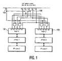
- FIG. 1is a high-level schematic block diagram of a SoC that includes a pair of IP cores, each having associated TAP controller/JTAG circuitry, and the logic and external connections for switching between each of the pair of IP cores for test access.
- FIG. 2is a high level block diagram of a SoC that includes a pair of IP cores, each having an associated switch register in accordance with the present invention, and the logic for internally generating a signal used in switching between each of the pair of IP cores for test access.
- FIG. 3is a high-level schematic block diagram of a SoC having a pair of TAP controllers illustrating the daisy chained data flow therebetween, in accordance with the present invention.
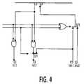
- FIG. 4is a schematic diagram of logic for implementing the daisy chained data flow illustrated in FIG. 3 , and the switching mechanism based on the mode signal.
- FIG. 5is a high-level schematic block diagram of showing conventional JTAG registers along with the switch register and chain register of the present invention.
- FIG. 6is a flowchart of an illustrative process in accordance with the present invention.
- Various embodiments of the present inventionallow multiple TAP controllers on a single integrated circuit to be accessed in a controlled manner through a single TAP controller by including a bit in a data register of each of the TAP controllers, along with simple combinational logic. Addition of such user data registers is allowed in accordance with the IEEE 1149 specification.
- ASICApplication Specific Integrated Circuit
- IP coreis context sensitive and may refer to either a design for a high-level functional block (e.g., schematic, hardware description language, netlist), or to an actual physical implementation of the high-level functional block. IP cores may include, in addition to the circuitry for implementation of the desired function, circuitry for implementation of test and debug facilities.
- JTAGrefers to the Joint Test Action Group.
- IEEEInstitute of Electrical and Electronic Engineers
- SoCrefers to a System on a Chip, with SoCs being the plural of SoC.
- microelectronic devicemay be considered to be the broadest term, encompassing the others.
- signalsare coupled between them and other circuit elements via physical, electrically conductive connections.
- the point of connectionis sometimes referred to as an input, output, terminal, line, pin, pad, port, interface, or similar variants and combinations.
- a JTAG compliant deviceincludes pins for clock, input data, output data, and mode selection, referred to, respectively, as TCK, TDI, TDO, and TMS.
- TCKrefers to Test Clock Input which is a terminal of the JTAG compliant device that receives a clock signal separate from the system clock.
- TDIrefers to a Test Data In which is a terminal through which data is shifted into the JTAG compliant device.
- TDOrefers to Test Data Out which is a terminal through which data is shifted out of the JTAG compliant device.
- TMSrefers to Test Mode Select which is a terminal which receives data for determining which of one or more test modes in which the JTAG compliant device is to operate.
- a JTAG compliant devicemay be any type of integrated circuit such as, for example, a microprocessor, an ASIC, or a SoC.
- a JTAG compliant devicemay also include a pin to receive a low active reset signal, referred to as TRST#.
- JTAG compliant devicesinclude a boundary scan register and a TAP controller.
- the TAP controlleris a state machine that controls the JTAG functions.
- the boundary scan registeris made up of a number of serially connected bits where each of those bits is also coupled to digital pins of the JTAG compliant device.
- JTAG compliant devicesmay also include other registers, such as, a data register, an instruction register, and a bypass register.
- the logical facilities defined by the IEEE 1149.1 specificationare commonly used for boundary scan testing and for system debug.
- Various embodiments of the present inventionprovide a mechanism for accessing one or more of the multiple TAP controllers within a SoC, while maintaining compliance with the IEEE 1149.1 specification.
- Simple embodiments of the present inventionallow a programmable switch from a default TAP controller to a second TAP controller. In this way the state of a SoC, as observed from outside the SoC, is compliant with the IEEE 1149.1 specification at start-up (i.e., after a reset has been applied to the system). More complex embodiments allow for arrangements such as switching back and forth between individual TAP controllers; and daisy-chaining all the TAP controllers together.
- An application of the present inventionis to provide access to multiple TAP controllers on a single chip while complying with the standard set forth in the IEEE 1149.1 specification.
- each TAP controllercontrols the test-logic (e.g., boundary scan testing) or the debug features of an associated IP core.
- no additional controllerse.g., top-level TAP, hierarchical TAP, Master TAP, or TAP Linking Module
- no additional pinsare needed to force a particular mode of operation on the chip.
- Embodiments of the present inventionare programmable through, for example, the standard JTAG ports.
- Embodiments of the present inventionare particularly useful in situations where the design of the TAP controllers and the IP cores are done separately, or at different points in time. Some embodiments of the present invention advantageously provide a modular, scalable approach to integrating multiple TAP controllers into a SoC.
- IP integratorwishes to put two or more IP cores on one SoC.
- the IP corescould be processors, DSPs, highly integrated functional blocks, or any combination of the foregoing.
- each of these IP coreshas a TAP controller and an associated JTAG module arranged in such a way that this TAP-JTAG combination forms an IEEE 1149.1 compliant device if it were on a chip by itself.
- a straightforward implementation for observing the two IP cores through a JTAG interfacewould use logical gating, multiplexing, and a “mode” pin as shown in FIG. 1 .
- TAP 1 102is the default TAP controller and that the mode signal received from a mode pin 104 is set to zero at start-up.
- both the TDI and TMS inputs to TAP 1 102 and TAP 2 106are logically gated such that when the mode signal is a logical zero, TAP 1 102 receives the actual TDI and TMS signals while TAP 2 106 receives zeroes for those inputs; and when the mode signal is a logical one, TAP 2 106 receives the actual TDI and TMS signals while TAP 1 102 receives zeroes for those inputs.
- the physical implementation of such logic circuitryis a matter well understood by those skilled in the art.
- TAP 1 102 or TAP 2 106the only output from either TAP 1 102 or TAP 2 106 is TDO.
- the other pins of TAP controllers 102 , 106are inputs.
- the finite state machine (FSM) of the TAP controllers 102 , 106will default to the Run-Test-Idle state within five cycles of the clock signal received on the TCK pin if the signal received from the TMS pin is zero.
- the TDI, TCK, TRSTN signalsmay be freely shared among TAP controllers 102 , 106 (but TDI in addition to TMS are logically gated as shown in FIG. 1 ).
- the TDO outputsare multiplexed by a 2-to-1 multiplexer 108 , as are the two enable signals (not shown) for the tri-state buffer associated with the TDO outputs. It is not an uncommon practice that the TAP controller, JTAG module, and IP core are designed separately, and at different points in time. The IP integrator has the task to connect the standardized interfaces properly.
- each JTAG module 202 , 204contains several JTAG registers, such as, for example, an instruction register 206 , a bypass register 208 , and an IDCODE register 210 .
- the IEEE 1149.1 standardallows extending JTAG modules 202 , 204 by user-defined data registers.
- a one bit data register 212is added to at least the default TAP controller. Such a one bit data register is referred to herein as the switch register 212 .
- FIG. 2shows a switch register 212 incorporated into each of the two JTAG modules 202 , 204 of this illustrative embodiment of the present invention.
- each of the one bit switch registers 212are coupled to an XOR gate 214 to produce the mode signal that controls the logical gating and multiplexing shown in FIG. 1 . That is, the mode signal which is produced within the integrated circuit, in accordance with the present invention, replaces the externally supplied mode signal, and corresponding mode pin, shown in FIG. 1 .
- the two TAP controllerswill appear to be one TAP controller to an off-chip observer, such as a JTAG probe.
- a JTAG probeThis is because the state that updates a data register transitions into the Run-Test-Idle state with one more high-level value on TMS during a TCK clock edge.
- the probeis negotiating the JTAG protocol, the hardware reconfigures itself and a different TAP controller is connected to the external interface pins of the SoC.
- the fact that the protocolcan be used during this particular state transition for the purpose of changing the connections of the TAP controllers themselves is used by embodiments of the present invention.
- JTAG operationsare that a new value is shifted into a register while, typically, the old value is shifted out and captured off-chip. In some cases a different value is shifted out, for example, when shifting in a new instruction.
- a JTAG probeshould not be required to keep track of the current values for different switch registers 212 . Therefore, in an embodiment of the present invention, the content of switch register 212 is inverted when shifting in a logical one. So regardless of the current values of both switch registers 212 , if exactly one input is inverted, the mode signal will switch. Such an arrangement is suitable for embodiments of the present invention in which two TAP controllers are integrated in a single chip.
- FIGS. 3 and 4the technique shown in FIG. 2 is extended to provide the data-flow associated daisy chaining. More particularly, the general data flow associated with daisy chaining is shown in FIG. 3 by only presenting the flow from TDI to TDO.
- a TAP controllere.g., TAP 1 102
- FIG. 5illustrates the conventional instruction, bypass, and IDCODE JTAG registers 206 , 208 , 210 , and the switch and chain registers 212 , 502 of the present invention.
- the chain signalcan now be used in addition to the mode signal to implement appropriate logical gating and multiplexing for TDI 1 , TDI 2 , TDO 1 and TDO 2 .
- FIG. 4is logically equivalent to FIG. 3 . It will be appreciated that this is an illustrative embodiment of the present invention, and that the exemplary logic may be different if the value of the mode signal, for example, is chosen to be different. This is well-understood by those skilled in the art.
- FIG. 6illustrates a process flow in accordance with the present invention.
- Switch register bits in two or more TAP controllersare reset 602 to a known state.
- a logical combination of the outputs of the switch register bits in their reset statecontrols which of the TAP controllers can be accessed by an external observer.
- writing to the switch register bit of the selected TAP controllerresults in that bit toggling (i.e., having its current state inverted).
- the new state of the switch register bitsis used to produce, or derive, 604 at least one mode signal.
- a next TAP controlleris selected 606 for communication with the external observer. In the case of two TAP controllers, the mode signal always selects one of the two TAP controllers.
- a mode busmay be derived, such that a changing value in any switch-register causes the next scheduled TAP controller to be selected. Such examples are described in greater detail below.
- TAP 1a TAP controller
- TAP 2a TAP controller
- TAP 3a mode bus
- TAP 1is selected by default, and when the switch register of a selected TAP controller is written, a next controller is selected, for example: TAP 1 ->TAP 2 ->TAP 3 ->TAP 1 and so on.
- the mode-bushas a width corresponding to ceiling[log 2(#TAPs)], which, in this illustrative embodiment, amounts to two bits, and those two bits may be defined as shown in TABLE 1.
- the logic for the mode-busis solely dependent on the value of the three switch register bits, S 1 , S 2 and S 3 , as shown in TABLE 2.
- the TDI and TMS inputsare gated by a 3-input AND gate (see TABLE 1).
- Two of the inputsare the mode[1] and mode[0] bits, with some inverting, such that only the selected TAP controller receives a TDI or TMS signal from the top-level pins.
- the three TDO signalsare multiplexed using the mode[1:0] bits such that only the selected TAP controller provides a TDO signal to the top-level pins.
- Various well-known circuitscan be used to implement the foregoing logic and multiplexing.
- the input-output table (see TABLE 2) for the mode-buscan be easily synthesized and yields an relatively small number of logic gates.
- TAP 1 to TAP 4in this example
- TAP 1is selected by default.
- a next controlleris selected, for example: TAP 1 ->TAP 2 ->TAP 3 ->TAP 4 ->TAP 1 and so on.
- the mode-bushas a width corresponding to ceiling[log 2(#TAPs)] (which still amounts to two bits), and the mode bits are defined in TABLE 3.
- the logic for the mode-busis solely dependent on the value of the four switch register bits, S 1 , S 2 , S 3 and S 4 , as shown in TABLE 4.
- the TDI and TMS inputsare gated by a 3-input AND gate (see TABLE 3). Two of the inputs are the mode[1] and mode[0] bits, with some inverting, such that only the selected TAP controller receives a TDI or TMS signal from the top-level pins. Similarly, the four TDO signals are multiplexed using the mode[1:0] bits such that only the selected TAP controller provides a TDO signal to the top-level pins.
- Various well-known circuitscan be used to implement the foregoing logic and multiplexing.
- the number of mode bitsgrows with log 2 rate. That is, three mode bits are sufficient for up to eight TAP controllers, four bits are sufficient up to sixteen TAP controllers and so on.
- the number of defined and used input statesalso grows slowly, only by two states per added TAP controller.
- every TDI in a chainis configured to receive its signal from two sources, namely: (1) the top-level TDI pin in case it is the TDI of the selected TAP controller, or, the TDO-signal from the preceding TAP controller in case of chaining.
- the complexitydoes not grow with the addition of more TAP controllers.
- the TDI for any TAP controller in the chaincan still only come from two possible sources, which are, as noted above: (1) the top-level TDI for the case of being the TDI of the selected controller, or, (2) from the TDO signal of the preceding TAP controller for the case of being a TDI of a daisy-chained TAP controller.
- the TDO pinis either driven by an individual selected TAP controller (using an n-to-1 multiplexer), or, if all TAP controllers are daisy-chained, the TDO is driven by the TDO-signal from the last TAP in the chain.
- Embodiments of the present inventionmay use scheduling algorithms other than round-robin, although there are some complexity issues in making the target of a switch programmable.
- the state of the systemmay be stored in every TAP controller, or in a central place. This is different from the above-described illustrative embodiments wherein the state is encoded in the combined switch/chain bits of the data registers in the TAP controllers.
- TAP controllers on a single chipare accessed, in accordance with the IEEE 1149 specification by maintaining the appearance of having only a single test access port to an outside observer.
- TAP controllersBy adding a single bit to a data register of each of a plurality of TAP controllers, along with straightforward combinational glue logic, the plurality of TAP controllers can be accessed without the need for additional chip pins, and without the need for additional TAP controllers.
- By adding a second bit to at least one of the TAP controllersinternal derivation of signals suitable for controlling desirable functionality of the plurality of TAP controllers can be achieved. Toggling the state of the added bits in the respective data registers of the plurality of TAP controllers provides the control information for either switching or daisy-chaining of the plurality of TAP controllers.
Landscapes
- Engineering & Computer Science (AREA)
- General Engineering & Computer Science (AREA)
- Physics & Mathematics (AREA)
- General Physics & Mathematics (AREA)
- Tests Of Electronic Circuits (AREA)
- Test And Diagnosis Of Digital Computers (AREA)
- Burglar Alarm Systems (AREA)
- Sink And Installation For Waste Water (AREA)
- Fire-Detection Mechanisms (AREA)
- For Increasing The Reliability Of Semiconductor Memories (AREA)
- Testing Or Calibration Of Command Recording Devices (AREA)
Abstract
Description
| TABLE 1 | |
| mode[1:0] | selected TAP |
| 00 | TAP1 |
| 01 | TAP2 |
| 10 | TAP3 |
| 11 | not used |
| TABLE 2 | |||||
| select, | |||||
| inputs | S3 | S2 | S1 | mode output | Operation in this mode: |
| 0 | 0 | 0 | TAP, 00 | S1 switch makes input = 001 | |
| 0 | 0 | 1 | TAP2, 01 | S2 switch makes input = 011 | |
| 0 | 1 | 1 | TAP3, 10 | S3 switch makes input = 111 | |
| 1 | 1 | 1 | TAP1, 00 | S1 switch makes input = 110 | |
| 1 | 1 | 0 | TAP2, 01 | S2 switch makes input = 10 | |
| 1 | 0 | 0 | TAP3, 10 | S3 switch makes input = 000 | |
| others | not used | remaining input combinations | ||
| not used | ||||
| TABLE 3 | ||
| selected TDO (mode-bus | ||
| mode[1:0] | selected TAP | is input to 4-to-1 mux) |
| “00” | TAP1 | tdo1 |
| “01” | TAP2 | tdo2 |
| “10” | TAP3 | tdo3 |
| “11” | TAP4 | tdo4 |
| TABLE 4 | ||||||
| select, | ||||||
| inputs | S4 | S3 | S2 | S1 | mode output | Operation in this mode |
| 0 | 0 | 0 | 0 | TAP1, 00 | S1 switch makes input = 0001 | |
| 0 | 0 | 0 | 1 | TAP2, 01 | S2 switch makes input = 0011 | |
| 0 | 0 | 1 | 1 | TAP3, 10 | S3 switch makes input = 0111 | |
| 0 | 1 | 1 | 1 | TAP4, 11 | S4 switch makes input = 1111 | |
| 1 | 1 | 1 | 1 | TAP1, 00 | S1 switch makes input = 1110 | |
| 1 | 1 | 1 | 0 | TAP2, 01 | S2 switch makes input = 1100 | |
| 1 | 1 | 0 | 0 | TAP3, 10 | S3 switch makes input = 1000 | |
| 1 | 0 | 0 | 0 | TAP4, 11 | S4 switch makes input = 0000 | |
| others | not used | remaining input states not | ||
| used | ||||
Claims (15)
Priority Applications (1)
| Application Number | Priority Date | Filing Date | Title |
|---|---|---|---|
| US10/539,104US7426670B2 (en) | 2002-12-20 | 2003-12-15 | Connecting multiple test access port controllers on a single test access port |
Applications Claiming Priority (4)
| Application Number | Priority Date | Filing Date | Title |
|---|---|---|---|
| US43539502P | 2002-12-20 | 2002-12-20 | |
| US60435395 | 2002-12-20 | ||
| PCT/IB2003/005950WO2004057357A1 (en) | 2002-12-20 | 2003-12-15 | Connecting multiple test access port controllers through a single test access port |
| US10/539,104US7426670B2 (en) | 2002-12-20 | 2003-12-15 | Connecting multiple test access port controllers on a single test access port |
Publications (2)
| Publication Number | Publication Date |
|---|---|
| US20060090110A1 US20060090110A1 (en) | 2006-04-27 |
| US7426670B2true US7426670B2 (en) | 2008-09-16 |
Family
ID=32682232
Family Applications (1)
| Application Number | Title | Priority Date | Filing Date |
|---|---|---|---|
| US10/539,104Expired - LifetimeUS7426670B2 (en) | 2002-12-20 | 2003-12-15 | Connecting multiple test access port controllers on a single test access port |
Country Status (10)
| Country | Link |
|---|---|
| US (1) | US7426670B2 (en) |
| EP (1) | EP1579229B1 (en) |
| JP (1) | JP2006510980A (en) |
| KR (1) | KR20050084395A (en) |
| CN (1) | CN100442074C (en) |
| AT (1) | ATE346309T1 (en) |
| AU (1) | AU2003288584A1 (en) |
| DE (1) | DE60309931T2 (en) |
| TW (1) | TWI298099B (en) |
| WO (1) | WO2004057357A1 (en) |
Cited By (7)
| Publication number | Priority date | Publication date | Assignee | Title |
|---|---|---|---|---|
| US20130124934A1 (en)* | 2011-10-01 | 2013-05-16 | Keith A. Jones | Packetizing jtag across industry standard interfaces |
| WO2014209347A1 (en)* | 2013-06-28 | 2014-12-31 | Intel Corporation | Mechanism to control resource utilization with adaptive routing |
| US20150046763A1 (en)* | 2013-08-12 | 2015-02-12 | Apple Inc. | Apparatus and Method for Controlling Internal Test Controllers |
| US20150095706A1 (en)* | 2007-06-07 | 2015-04-02 | Texas Instruments Incorporated | Offline at start up of a powered on device |
| US9810739B2 (en) | 2015-10-27 | 2017-11-07 | Andes Technology Corporation | Electronic system, system diagnostic circuit and operation method thereof |
| US10890619B2 (en) | 2017-08-23 | 2021-01-12 | Stmicroelectronics International N.V. | Sequential test access port selection in a JTAG interface |
| US20220043058A1 (en)* | 2008-03-14 | 2022-02-10 | Texas Instruments Incorporated | Addressable test access port method and apparatus |
Families Citing this family (18)
| Publication number | Priority date | Publication date | Assignee | Title |
|---|---|---|---|---|
| US7417450B2 (en) | 2005-12-02 | 2008-08-26 | Texas Instruments Incorporated | Testing combinational logic die with bidirectional TDI-TMS/TDO chanel circuit |
| US7346821B2 (en)* | 2003-08-28 | 2008-03-18 | Texas Instrument Incorporated | IC with JTAG port, linking module, and off-chip TAP interface |
| GB0526448D0 (en)* | 2005-12-23 | 2006-02-08 | Advanced Risc Mach Ltd | Diagnostic mode switching |
| KR100809259B1 (en)* | 2006-10-04 | 2008-03-03 | 삼성전기주식회사 | Communication module interface device |
| JP2008310792A (en)* | 2007-05-11 | 2008-12-25 | Nec Electronics Corp | Test circuit |
| JP5022110B2 (en)* | 2007-06-05 | 2012-09-12 | ルネサスエレクトロニクス株式会社 | Semiconductor integrated circuit |
| US7783819B2 (en) | 2008-03-31 | 2010-08-24 | Intel Corporation | Integrating non-peripheral component interconnect (PCI) resources into a personal computer system |
| WO2010035238A1 (en)* | 2008-09-26 | 2010-04-01 | Nxp B.V. | Method for testing a partially assembled multi-die device, integrated circuit die and multi-die device |
| US8694844B2 (en)* | 2010-07-29 | 2014-04-08 | Texas Instruments Incorporated | AT speed TAP with dual port router and command circuit |
| US9323633B2 (en)* | 2013-03-28 | 2016-04-26 | Stmicroelectronics, Inc. | Dual master JTAG method, circuit, and system |
| KR102474620B1 (en)* | 2016-01-25 | 2022-12-05 | 삼성전자주식회사 | Semiconductor device, semiconductor system and method for operating semiconductor device |
| CN108226740B (en)* | 2016-12-09 | 2020-06-02 | 英业达科技有限公司 | Expansion circuit board for providing interface of expansion joint test working group |
| CN108829547B (en)* | 2018-05-15 | 2021-11-16 | 中国船舶重工集团公司第七一九研究所 | Computer controller of ocean platform and implementation method thereof |
| US10571518B1 (en)* | 2018-09-26 | 2020-02-25 | Nxp B.V. | Limited pin test interface with analog test bus |
| CN109406902B (en)* | 2018-11-28 | 2021-03-19 | 中科曙光信息产业成都有限公司 | Logic scanning aging test system |
| CN113627106B (en)* | 2021-08-04 | 2022-02-15 | 北京华大九天科技股份有限公司 | Simulation method and device of multi-bit register and electronic equipment |
| CN116774018B (en)* | 2023-08-22 | 2023-11-28 | 北京芯驰半导体科技有限公司 | Chip testing method and device and electronic equipment |
| CN117741411A (en)* | 2024-02-19 | 2024-03-22 | 西安简矽技术有限公司 | Chip adjusting system and method |
Citations (8)
| Publication number | Priority date | Publication date | Assignee | Title |
|---|---|---|---|---|
| US5627842A (en) | 1993-01-21 | 1997-05-06 | Digital Equipment Corporation | Architecture for system-wide standardized intra-module and inter-module fault testing |
| US6073254A (en)* | 1996-08-30 | 2000-06-06 | Texas Instruments Incorporated | Selectively accessing test access ports in a multiple test access port environment |
| US6311302B1 (en) | 1999-04-01 | 2001-10-30 | Philips Semiconductor, Inc. | Method and arrangement for hierarchical control of multiple test access port control modules |
| US6385749B1 (en)* | 1999-04-01 | 2002-05-07 | Koninklijke Philips Electronics N.V. (Kpenv) | Method and arrangement for controlling multiple test access port control modules |
| US20020184562A1 (en)* | 2001-04-27 | 2002-12-05 | Benoit Nadeau-Dostie | Method of designing circuit having multiple test access ports, circuit produced thereby and method of using same |
| US6804725B1 (en)* | 1996-08-30 | 2004-10-12 | Texas Instruments Incorporated | IC with state machine controlled linking module |
| US6961884B1 (en)* | 2000-06-12 | 2005-11-01 | Altera Corporation | JTAG mirroring circuitry and methods |
| US6968408B2 (en)* | 2002-08-08 | 2005-11-22 | Texas Instruments Incorporated | Linking addressable shadow port and protocol for serial bus networks |
Family Cites Families (4)
| Publication number | Priority date | Publication date | Assignee | Title |
|---|---|---|---|---|
| US5132635A (en)* | 1991-03-05 | 1992-07-21 | Ast Research, Inc. | Serial testing of removable circuit boards on a backplane bus |
| FI100136B (en)* | 1993-10-01 | 1997-09-30 | Nokia Telecommunications Oy | Procedure for testing an integrated circuit and an integrated circuit s |
| US6032279A (en)* | 1997-11-07 | 2000-02-29 | Atmel Corporation | Boundary scan system with address dependent instructions |
| WO2001053844A1 (en)* | 2000-01-18 | 2001-07-26 | Cadence Design Systems, Inc. | Hierarchical test circuit structure for chips with multiple circuit blocks |
- 2003
- 2003-12-15USUS10/539,104patent/US7426670B2/ennot_activeExpired - Lifetime
- 2003-12-15EPEP03780425Apatent/EP1579229B1/ennot_activeExpired - Lifetime
- 2003-12-15AUAU2003288584Apatent/AU2003288584A1/ennot_activeAbandoned
- 2003-12-15WOPCT/IB2003/005950patent/WO2004057357A1/enactiveIP Right Grant
- 2003-12-15ATAT03780425Tpatent/ATE346309T1/ennot_activeIP Right Cessation
- 2003-12-15JPJP2004561840Apatent/JP2006510980A/enactivePending
- 2003-12-15CNCNB2003801068393Apatent/CN100442074C/ennot_activeExpired - Fee Related
- 2003-12-15DEDE60309931Tpatent/DE60309931T2/ennot_activeExpired - Lifetime
- 2003-12-15KRKR1020057011239Apatent/KR20050084395A/ennot_activeCeased
- 2003-12-17TWTW092135815Apatent/TWI298099B/ennot_activeIP Right Cessation
Patent Citations (10)
| Publication number | Priority date | Publication date | Assignee | Title |
|---|---|---|---|---|
| US5627842A (en) | 1993-01-21 | 1997-05-06 | Digital Equipment Corporation | Architecture for system-wide standardized intra-module and inter-module fault testing |
| US6073254A (en)* | 1996-08-30 | 2000-06-06 | Texas Instruments Incorporated | Selectively accessing test access ports in a multiple test access port environment |
| US6804725B1 (en)* | 1996-08-30 | 2004-10-12 | Texas Instruments Incorporated | IC with state machine controlled linking module |
| US20050050413A1 (en)* | 1996-08-30 | 2005-03-03 | Whetsel Lee D. | Selectively accessing test access ports in a multiple test access port environment |
| US6311302B1 (en) | 1999-04-01 | 2001-10-30 | Philips Semiconductor, Inc. | Method and arrangement for hierarchical control of multiple test access port control modules |
| US6385749B1 (en)* | 1999-04-01 | 2002-05-07 | Koninklijke Philips Electronics N.V. (Kpenv) | Method and arrangement for controlling multiple test access port control modules |
| US6961884B1 (en)* | 2000-06-12 | 2005-11-01 | Altera Corporation | JTAG mirroring circuitry and methods |
| US20020184562A1 (en)* | 2001-04-27 | 2002-12-05 | Benoit Nadeau-Dostie | Method of designing circuit having multiple test access ports, circuit produced thereby and method of using same |
| US6829730B2 (en)* | 2001-04-27 | 2004-12-07 | Logicvision, Inc. | Method of designing circuit having multiple test access ports, circuit produced thereby and method of using same |
| US6968408B2 (en)* | 2002-08-08 | 2005-11-22 | Texas Instruments Incorporated | Linking addressable shadow port and protocol for serial bus networks |
Cited By (12)
| Publication number | Priority date | Publication date | Assignee | Title |
|---|---|---|---|---|
| US20150095706A1 (en)* | 2007-06-07 | 2015-04-02 | Texas Instruments Incorporated | Offline at start up of a powered on device |
| US9977079B2 (en)* | 2007-06-07 | 2018-05-22 | Texas Instruments Incorporated | Operating two tap system after detecting shared bus synchronization sequence |
| US20220043058A1 (en)* | 2008-03-14 | 2022-02-10 | Texas Instruments Incorporated | Addressable test access port method and apparatus |
| US11747397B2 (en)* | 2008-03-14 | 2023-09-05 | Texas Instruments Incorporated | Addressable test access port apparatus |
| US12050247B2 (en) | 2008-03-14 | 2024-07-30 | Texas Instruments Incorporated | Addressable test access port |
| US20130124934A1 (en)* | 2011-10-01 | 2013-05-16 | Keith A. Jones | Packetizing jtag across industry standard interfaces |
| US9015542B2 (en)* | 2011-10-01 | 2015-04-21 | Intel Corporation | Packetizing JTAG across industry standard interfaces |
| WO2014209347A1 (en)* | 2013-06-28 | 2014-12-31 | Intel Corporation | Mechanism to control resource utilization with adaptive routing |
| US9294403B2 (en) | 2013-06-28 | 2016-03-22 | Intel Corporation | Mechanism to control resource utilization with adaptive routing |
| US20150046763A1 (en)* | 2013-08-12 | 2015-02-12 | Apple Inc. | Apparatus and Method for Controlling Internal Test Controllers |
| US9810739B2 (en) | 2015-10-27 | 2017-11-07 | Andes Technology Corporation | Electronic system, system diagnostic circuit and operation method thereof |
| US10890619B2 (en) | 2017-08-23 | 2021-01-12 | Stmicroelectronics International N.V. | Sequential test access port selection in a JTAG interface |
Also Published As
| Publication number | Publication date |
|---|---|
| JP2006510980A (en) | 2006-03-30 |
| TWI298099B (en) | 2008-06-21 |
| EP1579229B1 (en) | 2006-11-22 |
| US20060090110A1 (en) | 2006-04-27 |
| EP1579229A1 (en) | 2005-09-28 |
| TW200500620A (en) | 2005-01-01 |
| DE60309931T2 (en) | 2007-09-13 |
| CN1729401A (en) | 2006-02-01 |
| AU2003288584A1 (en) | 2004-07-14 |
| DE60309931D1 (en) | 2007-01-04 |
| WO2004057357A1 (en) | 2004-07-08 |
| ATE346309T1 (en) | 2006-12-15 |
| CN100442074C (en) | 2008-12-10 |
| KR20050084395A (en) | 2005-08-26 |
Similar Documents
| Publication | Publication Date | Title |
|---|---|---|
| US7426670B2 (en) | Connecting multiple test access port controllers on a single test access port | |
| US10281524B2 (en) | Test partition external input/output interface control for test partitions in a semiconductor | |
| US10162001B2 (en) | TAP and gating enable, CaptureDR, capture, and gated CaptureDR signals | |
| JP4422427B2 (en) | Single chip system and method for testing / debugging this system | |
| US6499124B1 (en) | Intest security circuit for boundary-scan architecture | |
| US6314539B1 (en) | Boundary-scan register cell with bypass circuit | |
| US6378090B1 (en) | Hierarchical test access port architecture for electronic circuits including embedded core having built-in test access port | |
| JP2994666B2 (en) | Boundary scanning test cell | |
| US20140229780A1 (en) | Ieee 1149.1 and p1500 test interfaces combined circuits and processes | |
| US20160349320A1 (en) | Remote bus wrapper for testing remote cores using automatic test pattern generation and other techniques | |
| US5260948A (en) | Bidirectional boundary-scan circuit | |
| US6381717B1 (en) | Snoopy test access port architecture for electronic circuits including embedded core having test access port with instruction driven wake-up | |
| EP1520182B1 (en) | Method and control circuitry for accessing multiple taps (test access ports) via a single tap | |
| US20030046625A1 (en) | Method and apparatus for efficient control of multiple tap controllers | |
| US7219281B2 (en) | Boundary scan of integrated circuits | |
| JP3987585B2 (en) | Core test control | |
| JP3207245B2 (en) | Circuit for JTAG architecture | |
| US20050015689A1 (en) | Electronic component and method for measuring its qualification | |
| US4894800A (en) | Reconfigurable register bit-slice for self-test | |
| US7761760B2 (en) | Integrated circuit and a method for designing a boundary scan super-cell | |
| KR100571633B1 (en) | System-on-chip with shift register chain circuitry for testing embedded core circuitry | |
| JP2004004047A (en) | Input/output characterization chain for integrated circuit | |
| US20030149926A1 (en) | Single scan chain in hierarchiacally bisted designs |
Legal Events
| Date | Code | Title | Description |
|---|---|---|---|
| AS | Assignment | Owner name:KONINKLIJKE PHILIPS ELECTRONICS N.V., NETHERLANDS Free format text:ASSIGNMENT OF ASSIGNORS INTEREST;ASSIGNOR:STEINBUSCH, OTTO;REEL/FRAME:017329/0899 Effective date:20030825 | |
| AS | Assignment | Owner name:NXP B.V., NETHERLANDS Free format text:ASSIGNMENT OF ASSIGNORS INTEREST;ASSIGNOR:KONINKLIJKE PHILIPS ELECTRONICS N.V.;REEL/FRAME:021085/0959 Effective date:20080423 Owner name:NXP B.V.,NETHERLANDS Free format text:ASSIGNMENT OF ASSIGNORS INTEREST;ASSIGNOR:KONINKLIJKE PHILIPS ELECTRONICS N.V.;REEL/FRAME:021085/0959 Effective date:20080423 | |
| STCF | Information on status: patent grant | Free format text:PATENTED CASE | |
| FPAY | Fee payment | Year of fee payment:4 | |
| AS | Assignment | Owner name:KONINKLIJKE PHILIPS ELECTRONICS N.V., NETHERLANDS Free format text:NUNC PRO TUNC ASSIGNMENT;ASSIGNOR:STEINBUSCH, OTTO;REEL/FRAME:035698/0604 Effective date:20150521 | |
| AS | Assignment | Owner name:III HOLDINGS 6, LLC, DELAWARE Free format text:ASSIGNMENT OF ASSIGNORS INTEREST;ASSIGNOR:NXP B.V.;REEL/FRAME:036304/0330 Effective date:20150730 | |
| FPAY | Fee payment | Year of fee payment:8 | |
| MAFP | Maintenance fee payment | Free format text:PAYMENT OF MAINTENANCE FEE, 12TH YEAR, LARGE ENTITY (ORIGINAL EVENT CODE: M1553); ENTITY STATUS OF PATENT OWNER: LARGE ENTITY Year of fee payment:12 | |
| AS | Assignment | Owner name:PURE POWER TECHNOLOGIES, INC., NORTH CAROLINA Free format text:RELEASE BY SECURED PARTY;ASSIGNOR:CERBERUS BUSINESS FINANCE, LLC;REEL/FRAME:064474/0910 Effective date:20230731 Owner name:STANADYNE LLC, NORTH CAROLINA Free format text:RELEASE BY SECURED PARTY;ASSIGNOR:CERBERUS BUSINESS FINANCE, LLC;REEL/FRAME:064474/0910 Effective date:20230731 |