US7425787B2 - Acoustic galvanic isolator incorporating single insulated decoupled stacked bulk acoustic resonator with acoustically-resonant electrical insulator - Google Patents
Acoustic galvanic isolator incorporating single insulated decoupled stacked bulk acoustic resonator with acoustically-resonant electrical insulatorDownload PDFInfo
- Publication number
- US7425787B2 US7425787B2US11/253,508US25350805AUS7425787B2US 7425787 B2US7425787 B2US 7425787B2US 25350805 AUS25350805 AUS 25350805AUS 7425787 B2US7425787 B2US 7425787B2
- Authority
- US
- United States
- Prior art keywords
- acoustic
- acoustically
- electrical insulator
- fbar
- resonant electrical
- Prior art date
- Legal status (The legal status is an assumption and is not a legal conclusion. Google has not performed a legal analysis and makes no representation as to the accuracy of the status listed.)
- Expired - Lifetime
Links
Images


Classifications
- H—ELECTRICITY
- H04—ELECTRIC COMMUNICATION TECHNIQUE
- H04B—TRANSMISSION
- H04B11/00—Transmission systems employing sonic, ultrasonic or infrasonic waves
- H—ELECTRICITY
- H03—ELECTRONIC CIRCUITRY
- H03H—IMPEDANCE NETWORKS, e.g. RESONANT CIRCUITS; RESONATORS
- H03H9/00—Networks comprising electromechanical or electro-acoustic elements; Electromechanical resonators
- H03H9/02—Details
- H03H9/02007—Details of bulk acoustic wave devices
- H—ELECTRICITY
- H03—ELECTRONIC CIRCUITRY
- H03H—IMPEDANCE NETWORKS, e.g. RESONANT CIRCUITS; RESONATORS
- H03H9/00—Networks comprising electromechanical or electro-acoustic elements; Electromechanical resonators
- H03H9/02—Details
- H03H9/125—Driving means, e.g. electrodes, coils
- H03H9/13—Driving means, e.g. electrodes, coils for networks consisting of piezoelectric or electrostrictive materials
- H03H9/132—Driving means, e.g. electrodes, coils for networks consisting of piezoelectric or electrostrictive materials characterized by a particular shape
- H—ELECTRICITY
- H03—ELECTRONIC CIRCUITRY
- H03H—IMPEDANCE NETWORKS, e.g. RESONANT CIRCUITS; RESONATORS
- H03H9/00—Networks comprising electromechanical or electro-acoustic elements; Electromechanical resonators
- H03H9/15—Constructional features of resonators consisting of piezoelectric or electrostrictive material
- H03H9/17—Constructional features of resonators consisting of piezoelectric or electrostrictive material having a single resonator
- H03H9/171—Constructional features of resonators consisting of piezoelectric or electrostrictive material having a single resonator implemented with thin-film techniques, i.e. of the film bulk acoustic resonator [FBAR] type
- H—ELECTRICITY
- H03—ELECTRONIC CIRCUITRY
- H03H—IMPEDANCE NETWORKS, e.g. RESONANT CIRCUITS; RESONATORS
- H03H9/00—Networks comprising electromechanical or electro-acoustic elements; Electromechanical resonators
- H03H9/46—Filters
- H03H9/54—Filters comprising resonators of piezoelectric or electrostrictive material
- H03H9/58—Multiple crystal filters
- H03H9/582—Multiple crystal filters implemented with thin-film techniques
- H03H9/583—Multiple crystal filters implemented with thin-film techniques comprising a plurality of piezoelectric layers acoustically coupled
- H03H9/584—Coupled Resonator Filters [CFR]
- H—ELECTRICITY
- H03—ELECTRONIC CIRCUITRY
- H03H—IMPEDANCE NETWORKS, e.g. RESONANT CIRCUITS; RESONATORS
- H03H9/00—Networks comprising electromechanical or electro-acoustic elements; Electromechanical resonators
- H03H9/46—Filters
- H03H9/54—Filters comprising resonators of piezoelectric or electrostrictive material
- H03H9/58—Multiple crystal filters
- H03H9/582—Multiple crystal filters implemented with thin-film techniques
- H03H9/586—Means for mounting to a substrate, i.e. means constituting the material interface confining the waves to a volume
- H03H9/587—Air-gaps
- H—ELECTRICITY
- H10—SEMICONDUCTOR DEVICES; ELECTRIC SOLID-STATE DEVICES NOT OTHERWISE PROVIDED FOR
- H10N—ELECTRIC SOLID-STATE DEVICES NOT OTHERWISE PROVIDED FOR
- H10N30/00—Piezoelectric or electrostrictive devices
- H10N30/40—Piezoelectric or electrostrictive devices with electrical input and electrical output, e.g. functioning as transformers
Definitions
- This disclosureis related to the following simultaneously-filed disclosures: Acoustic Galvanic Isolator Incorporating Single Decoupled Stacked Bulk Acoustic Resonator of John D. Larson III, publication No. 2007-0090892; Acoustic Galvanic Isolator Incorporating Film Acoustically-Coupled Transformer of John D. Larson III, publication No. 2007-0085631; Acoustic Galvanic Isolator Incorporating Series-Connected Decoupled Stacked Bulk Acoustic Resonators of John D. Larson III et al., publication No. 2007-0086080; and Acoustic Galvanic Isolator of John D. Larson III et al., publication No. 2007-0085632, all of which are assigned to the assignee of this disclosure at the time of filing and incorporated by reference.
- a galvanic isolatorallows an information signal to pass from its input to its output but has no electrical conduction path between its input and its output. The lack of an electrical conduction path allows the galvanic isolator to prevent unwanted voltages from passing between its input and its output. Strictly speaking, a galvanic isolator blocks only DC voltage, but a typical galvanic isolator additionally blocks a.c. voltage, such as voltages at power line and audio frequencies.
- An example of a galvanic isolatoris a data coupler that passes a high data rate digital information signal but blocks DC voltages and additionally blocks low-frequency a.c. voltages.
- a data coupleris an opto-isolator such as the opto-isolators sold by Agilent Technologies, Inc.
- an electrical information signalis converted to a light signal by a light-emitting diode (LED).
- the light signalpasses through an electrically non-conducting light-transmitting medium, typically an air gap or an optical waveguide, and is received by a photodetector.
- the photodetectorconverts the light signal back to an electrical signal.
- Galvanic isolationis provided because the light signal can pass through the electrically non-conducting light-transmitting medium without the need of metallic conductors.
- Other data couplersinclude a transformer composed of a first coil magnetically coupled to a second coil. Passing the electrical information signal through the first coil converts the electrical information signal to magnetic flux. The magnetic flux passes through air or an electrically non-conducting permeable magnetic material to the second coil. The second coil converts the magnetic flux back to an electrical signal.
- the transformerallows the high data rate information signal to pass but blocks transmission of DC voltages and low-frequency a.c. voltages.
- the resistance of the conveyor of the magnetic fluxis sufficient to prevent DC voltages and low-frequency a.c. voltages from passing from input to output. Blocking capacitors are sometimes used to provide similar isolation.
- Inexpensive opto-isolatorsare typically limited to data rates of about 10 Mb/s by device capacitance, and from power limitations of the optical devices.
- the transformer approachrequires that the coils have a large inductance yet be capable of transmitting the high data rate information signal. Such conflicting requirements are often difficult to reconcile.
- Using capacitorsdoes not provide an absolute break in the conduction path because the information signal is transmitted electrically throughout. More successful solutions convert the electrical information signal to another form of signal, e.g., light or a magnetic flux, and then convert the other form of signal back to an electrical signal. This allows the electrical path between input and output to be eliminated.
- the inventionprovides an acoustic galvanic isolator.
- Embodiments of the acoustic galvanic isolatorcomprise a carrier signal source, a modulator connected to receive an information signal and the carrier signal, a demodulator, and an electrically-isolating acoustic coupler connected between the modulator and the demodulator.
- the acoustic couplercomprises no more than one insulated decoupled stacked bulk acoustic resonator (IDSBAR) having an acoustically-resonant electrical insulator.
- IDSBARinsulated decoupled stacked bulk acoustic resonator
- the IDSBARcomprises a first film bulk acoustic resonator (FBAR), a second FBAR stacked on the first FBAR, and a first acoustic decoupler, the acoustically-resonant electrical insulator and a second acoustic decoupler located between the FBARs.
- the acoustically-resonant electrical insulatorcomprises a quarter-wave layer of electrically-insulating material and is located between the first acoustic decoupler and the second acoustic coupler.
- the acoustically-resonant electrical insulatoris a first acoustically-resonant electrical insulator and the IDSBAR additionally comprises a first FBAR, a second FBAR stacked on the first FBAR, and, between the FBARs, in order, the first acoustically-resonant electrical insulator, an acoustic decoupler and a second acoustically-resonant electrical insulator.
- each acoustically-resonant electrical insulatoris a half-wave acoustically-resonant electrical insulator and comprises a half-wave layer of electrically-insulating material.
- the inventionprovides a method for galvanically isolating an information signal.
- Embodiments of the methodcomprise providing an electrically-isolating acoustic coupler comprising no more than one insulated decoupled stacked bulk acoustic resonator (IDSBAR) having an acoustically-resonant electrical insulator; providing a carrier signal; modulating the carrier signal with the information signal to form a modulated electrical signal; acoustically coupling the modulated electrical signal through the electrically-isolating acoustic coupler; and recovering the information signal from the modulated electrical signal acoustically coupled through the electrically-isolating acoustic coupler.
- IDSBARinsulated decoupled stacked bulk acoustic resonator
- An electrically-isolating acoustic coupler based on a single IDSBARis physically small and is inexpensive to fabricate yet is capable of acoustically coupling information signals having data rates in excess of 100 Mbit/s and has a substantial breakdown voltage between its inputs and its outputs.
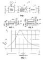
- FIG. 1is a block diagram showing an acoustic galvanic isolator in accordance with an embodiment of the invention.
- FIG. 2is a schematic diagram showing an example of an acoustic coupler that may be used as the electrically-isolating acoustic coupler of the acoustic galvanic isolator shown in FIG. 1 .
- FIG. 3is a schematic diagram showing an acoustic coupler in accordance with a first embodiment of the invention that may be used as the electrically-isolating acoustic coupler of the acoustic galvanic isolator shown in FIG. 1 .
- FIG. 4is a graph showing the frequency response characteristic of an exemplary embodiment of the insulating decoupled stacked bulk acoustic resonator (IDSBAR) that forms part of the acoustic coupler shown in FIG. 3 .
- IDSBARinsulating decoupled stacked bulk acoustic resonator
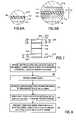
- FIG. 5Ais a plan view showing a practical example of the acoustic coupler shown in FIG. 3 .
- FIGS. 5B and 5Care cross-sectional views along section lines 5 B- 5 B and 5 C- 5 C, respectively, shown in FIG. 5A .
- FIG. 6Ais an enlarged view of the portion marked 6 A in FIG. 5B showing a first embodiment of the acoustic decoupler.
- FIG. 6Bis an enlarged view of the portion marked 6 A in FIG. 5B showing a second embodiment of the acoustic decoupler.
- FIG. 7is a schematic diagram showing an example of an acoustic coupler in accordance with a second embodiment of the invention that may be used as the electrically-isolating acoustic coupler of the acoustic galvanic isolator shown in FIG. 1 .
- FIG. 8Ais a plan view showing a practical example of the acoustic coupler shown in FIG. 7 .
- FIGS. 8B and 8Care cross-sectional views along section lines 8 B- 8 B and 8 C- 8 C, respectively, shown in FIG. 8A .
- FIG. 9is a flow chart showing an example of a method in accordance with an embodiment of the invention for galvanically isolating an information signal.
- FIG. 1is a block diagram showing an acoustic galvanic isolator 10 in accordance with an embodiment of the invention.
- Acoustic galvanic isolator 10transmits an electrical information signal S I between its input terminals and its output terminals yet provides electrical isolation between its input terminals and its output terminals.
- Acoustic galvanic isolator 10not only provides electrical isolation at DC but also provides a.c. electrical isolation.
- Electrical information signal S Iis typically a high data rate digital data signal, but may alternatively be an analog signal. In one application, electrical information signal S I is a 100 Mbit/sec Ethernet signal.
- acoustic galvanic isolator 10is composed of a local oscillator 12 , a modulator 14 , an electrically-isolating acoustic coupler 16 and a demodulator 18 .
- local oscillator 12is the source of an electrical carrier signal S C .
- Modulator 14has inputs connected to receive electrical information signal S I from input terminals 22 , 24 of acoustic galvanic isolator 10 and to receive carrier signal S C from local oscillator 12 .
- Modulator 14has outputs connected to inputs 26 , 28 of electrically-isolating acoustic coupler 16 .
- Outputs 32 , 34 of electrically-isolating acoustic coupler 16are connected to the inputs of demodulator 18 .
- the outputs of demodulator 18are connected to the output terminals 36 , 38 of acoustic galvanic isolator 10 .
- Electrically-isolating acoustic coupler 16has a band-pass frequency response that will be described in more detail below with reference to FIG. 4 .
- Local oscillator 12generates carrier signal S C at a frequency nominally at the center of the pass band of electrically-isolating acoustic coupler 16 .
- the pass band of electrically-isolating acoustic coupler 16is centered at a frequency of 1.9 GHz, and local oscillator 12 generated carrier signal S C at a frequency of 1.9 GHz.
- Local oscillator 12feeds carrier signal S C to the carrier signal
- Modulator 14receives electrical information signal S I from input terminals 22 , 24 and modulates carrier signal S C with electrical information signal S I to generate modulated electrical signal S M .
- modulated electrical signal S Mis carrier signal S C modulated in accordance with electrical information signal S I .
- Any suitable modulation schememay be used.
- carrier signalis amplitude modulated by electrical information signal S I and electrical information signal S I is a digital signal having low and high signal levels respectively representing 0s and 1s
- modulated electrical signal S Mhas small and large amplitudes respectively representing the 0s and 1s of the electrical information signal.
- electrically-isolating acoustic coupler 16acoustically couples modulated electrical signal S M from its inputs 26 , 28 to its outputs 32 , 34 to provide an electrical output signal S O to the inputs of demodulator 18 .
- Electrical output signal S Ois similar to modulated electrical signal S M , i.e., it is a modulated electrical signal having the same frequency as carrier signal S C , the same modulation scheme as modulated electrical signal and the same information content as electrical information signal S I .
- Demodulator 18demodulates electrical output signal S O to recover electrical information signal S I as recovered electrical information signal S R .
- Recovered electrical information signal S Ris output from demodulator 18 to output terminals 36 , 38 .
- Demodulator 18comprises a detector (not shown) that recovers electrical information signal S I from electrical output signal S O as is known in the art.
- the detectorrectifies and integrates electrical output signal S O to recover electrical information signal S I .
- demodulator 18additionally includes a clock and data recovery (CDR) circuit following the detector.
- the CDR circuitoperates to clean up the waveform of the raw electrical information signal recovered from the electrical output signal S O to generate recovered electrical information signal S R .
- Demodulator 18provides the recovered electrical information signal S R to the output terminals 36 , 38 of acoustic galvanic isolator 10 .
- local oscillator 12is shown as part of acoustic galvanic isolator 10 .
- acoustic galvanic isolator 10instead of a local oscillator, has carrier signal input terminals (not shown) via which the acoustic galvanic isolator receives the carrier signal S C from an external carrier signal generator.
- the carrier signal input terminalsprovide the carrier signal source for the acoustic galvanic isolator.
- Acoustic couplers in according with embodiments of the invention that can be used as electrically-isolating acoustic coupler 16 in acoustic galvanic isolator 10will now be described. Such embodiments all have a band-pass frequency response, as will be described in more detail below with reference to FIG. 4 .
- the pass-band of the acoustic coupleris characterized by a center frequency and a bandwidth.
- the bandwidth of the pass-banddetermines the maximum data rate of the information signal that can be acoustically coupled by the acoustic coupler.
- the center frequency of the pass band of the acoustic couplerwill be referred to as the center frequency of the acoustic coupler.
- the acoustic coupler embodimentsare composed in part of layers of various acoustically-transmissive materials whose thickness depends on the wavelength in the acoustically-transmissive material of an acoustic signal nominally equal in frequency to the center frequency of the acoustic coupler.
- the frequency of carrier signal S Cis nominally equal to the center frequency of the acoustic coupler used as electrically-isolating acoustic coupler 16 .
- quarter-wave layerwill be used to denote a layer of acoustically-transmissive material having a nominal thickness t equal to an odd integral multiple of one quarter of the wavelength in the material of an acoustic signal nominally equal in frequency to the center frequency of the acoustic coupler, i.e.: t ⁇ (2 m +1) ⁇ n /4 (1)
- ⁇ nis the wavelength of the above-mentioned acoustic signal in the acoustically-transmissive material
- mis an integer equal to or greater than zero.
- the thickness of a quarter-wave layermay differ from the nominal thickness by approximately ⁇ 10% of ⁇ n /4. A thickness outside this tolerance range can be used with some degradation in performance, but the thickness of a quarter-wave layer always differs significantly from an integral multiple of ⁇ n /2.
- a quarter wave layer having a thickness equal to a specific number of quarter wavelengths of the above-mentioned acoustic signal in the material of the layerwill be denoted by preceding the term quarter-wave layer by a number denoting the number of quarter wavelengths.
- a one quarter-wave layeris a quarter-wave layer of a least-possible thickness.
- half-wave layerwill be used to denote a layer of acoustically-transmissive material having a nominal thickness t equal to an integral multiple of one half of the wavelength in the material of an acoustic signal equal in frequency to the center frequency of the acoustic coupler, i.e.: t ⁇ n ⁇ n /2 (2) where n is an integer greater than zero.
- the thickness of a half-wave layermay differ from the nominal thickness by approximately ⁇ 10% of ⁇ n /2. A thickness outside this tolerance range can be used with some degradation in performance, but the thickness of a half-wave layer always differs significantly from an odd integral multiple of ⁇ n /4.
- the term half-wave layermay be preceded with a number to denote a layer having a thickness equal to a specific number of half wavelengths of the above-mentioned acoustic signal in the material of the layer.
- Acoustic galvanic isolators and their constituent electrically-isolating acoustic couplersare characterized by a breakdown voltage.
- the breakdown voltage of an acoustic galvanic isolatoris the voltage that, when applied between the input terminals and output terminals of the acoustic galvanic isolator, causes a leakage current greater than a threshold leakage current to flow.
- the input terminalsare electrically connected to one another and the output terminals are electrically connected to one another to make the breakdown voltage measurement.
- the breakdown voltage of an electrically-isolating acoustic coupleris the voltage that, when applied between the inputs and outputs of the acoustically-resonant electrical insulator, causes a leakage current greater than a threshold leakage current to flow.
- the inputsare electrically connected to one another and the outputs are electrically connected to one another to make the breakdown voltage measurement.
- the threshold leakage currentis application-dependent, and is typically of the order of microamps.
- FIG. 2is a schematic diagram of an exemplary embodiment 100 of an electrically-isolating acoustic coupler disclosed in the above-mentioned U.S. patent application entitled Acoustic Galvanic Isolator Incorporating Single Decoupled Stacked Bulk Acoustic Resonator of John D. Larson III assigned to the assignee of this application and incorporated by reference.
- Acoustic coupler 100comprises a single decoupled stacked bulk acoustic resonator (DSBAR) 106 , inputs 26 , 28 , outputs 32 , 34 , an electrical circuit 140 that connects DSBAR 106 to inputs 26 , 28 and an electrical circuit 141 that connects DSBAR 106 to outputs 32 , 34 .
- DSBAR 106incorporates an electrically-insulating acoustic decoupler 130 that provides electrical isolation between inputs 26 , 28 and outputs 32 , 34 .
- acoustic coupler 100When used as electrically-isolating acoustic coupler 16 in acoustic galvanic isolator 10 shown in FIG. 1 , acoustic coupler 100 acoustically couples modulated electrical signal S M from inputs 26 , 28 to outputs 32 , 34 while providing electrical isolation between inputs 26 , 28 and outputs 32 , 34 .
- acoustic coupler 100effectively galvanically isolates output terminals 36 , 38 from input terminals 22 , 24 , and allows the output terminals to differ in voltage from the input terminals by a voltage up to its specified breakdown voltage.
- DSBAR 106is composed of a lower film bulk acoustic resonator (FBAR) 110 , an upper FBAR 120 stacked on FBAR 110 , and an electrically-insulating acoustic decoupler 130 between lower FBAR 110 and upper FBAR 120 .
- FBAR 110is composed of opposed planar electrodes 112 and 114 and a piezoelectric element 116 between the electrodes.
- FBAR 120is composed of opposed planar electrodes 122 and 124 and a piezoelectric element 126 between the electrodes.
- Acoustic decoupler 130is located between electrode 114 of FBAR 110 and electrode 122 of FBAR 120 .
- Electrical circuit 140electrically connects electrodes 112 and 114 of FBAR 110 to inputs 26 , 28 , respectively.
- Electrical circuit 141electrically connects electrodes 122 and 124 of FBAR 120 to outputs 32 , 34 , respectively.
- Modulated electrical signal S M received at inputs 26 , 28applies a voltage between electrodes 112 and 114 of FBAR 110 .
- FBAR 110converts the modulated electrical signal S M to an acoustic signal. Specifically, the voltage applied to piezoelectric element 116 by electrodes 112 and 114 mechanically deforms piezoelectric element 116 , which causes FBAR 110 to vibrate mechanically at the frequency of the modulated electrical signal.
- Electrically-insulating acoustic coupler 130couples part of the acoustic signal generated by FBAR 110 to FBAR 120 . Additionally, electrically-insulating acoustic decoupler 130 is electrically insulating and therefore electrically isolates FBAR 120 from FBAR 110 . FBAR 120 receives the acoustic signal coupled by acoustic decoupler 130 and converts the acoustic signal back into an electrical signal that appears across piezoelectric element 126 . The electrical signal is picked up by electrodes 122 and 124 and is fed to outputs 32 , 34 , respectively, as electrical output signal S O .
- Electrical output signal S O appearing between outputs 32 , 34has the same frequency and includes the information content of the modulated electrical signal S M applied between inputs 26 , 28 .
- acoustic coupler 100effectively acoustically couples the modulated electrical signal S M from inputs 26 , 28 to outputs 32 , 34 .
- Acoustic decoupler 130controls the coupling of the acoustic signal generated by FBAR 110 to FBAR 120 and, hence, the bandwidth of acoustic coupler 100 . Specifically, due to a substantial mis-match in acoustic impedance between the acoustic decoupler and FBARs 110 and 120 , the acoustic decoupler couples less of the acoustic signal generated by FBAR 110 to FBAR 120 than would be coupled by direct contact between the FBARs.
- the breakdown voltage of acoustic galvanic isolator 10 between input terminals 22 , 24 and output terminals 36 , 38depends in a typical embodiment on the breakdown voltage of acoustic coupler 100 shown in FIG. 2 .
- the breakdown voltage of acoustic coupler 100depends in typical embodiments on the breakdown voltage of electrically-insulating acoustic decoupler 130 .
- acoustic decoupler 130is composed of a one quarter wave layer of acoustic decoupling material.
- a one quarter-wave layer of a typical acoustic decoupling materialis of the order of 200 nm thick.
- the breakdown voltage of an embodiment of acoustic coupler 100 incorporating such an acoustic decouplerdepends on the thickness of acoustic decoupling layer and the breakdown field of the acoustic decoupling material. Increasing the thickness of the acoustic decoupling layer increases the breakdown voltage of the acoustic coupler at the expense of a reduction in the signal integrity with which modulated electrical signal S M is coupled from inputs 26 , 28 to outputs 32 , 34 . This increases the difficulty of successfully recovering recovered electrical information signal S R from electrical output signal S O . The signal integrity of electrical output signal S O is degraded by the ability of the thicker acoustic decoupler to support multiple acoustic modes.
- acoustic decoupler 130is composed of an electrically-insulating Bragg structure.
- Embodiments of acoustic decoupler 130 in which the Bragg structure has more than one insulating layertypically have a greater breakdown voltage than embodiments composed of a single acoustic decoupling layer.
- Some galvanic isolatorsare required to have a breakdown voltage between their input terminals and output terminals of greater than one kilovolt.
- acoustic decoupler 130is the sole provider of electrical isolation between inputs 26 , 28 and outputs 32 , 34 .
- Embodiments of acoustic galvanic isolator 10 in which electrically-isolating acoustic coupler 16 is embodied as acoustic coupler 100have difficulty in meeting such breakdown voltage requirements.
- acoustic couplersin accordance with the invention have a substantially greater breakdown voltage than acoustic coupler 100 described above with reference to FIGS. 2 and 4 A- 4 C.
- FIG. 3is a schematic diagram showing an example of an acoustic coupler 200 in accordance with a first embodiment of the invention.
- Acoustic coupler 200comprises an insulated decoupled stacked bulk acoustic resonator (IDSBAR) 206 in accordance with a first IDSBAR embodiment.
- IDSBARinsulated decoupled stacked bulk acoustic resonator
- an IDSBAR in accordance with the first IDSBAR embodimenthas a first acoustic decoupler, a quarter-wave acoustically-resonant electrical insulator and a second acoustic decoupler in order between its constituent FBARs.
- IDSBAR 206 in accordance with the first IDSBAR embodimentgives acoustic coupler 200 a substantially greater breakdown voltage than acoustic coupler 100 described above with reference to FIG. 2 .
- acoustic coupler 200additionally comprises inputs 26 , 28 , outputs 32 , 34 , an electrical circuit 140 that connects IDSBAR 206 to inputs 26 , 28 , and an electrical circuit 141 that connects IDSBAR 206 to outputs 32 , 34 .
- acoustic coupler 200When used as electrically-isolating acoustic coupler 16 in acoustic galvanic isolator 10 shown in FIG. 1 , acoustic coupler 200 acoustically couples modulated electrical signal S M from inputs 26 , 28 to outputs 32 , 34 while providing electrical isolation between inputs 26 , 28 and outputs 32 , 34 .
- acoustic coupler 200effectively galvanically isolates output terminals 36 , 38 from input terminals 22 , 24 , and allows the output terminals to differ in voltage from the input terminals by a voltage up to its specified breakdown voltage.
- the exemplary embodiment of IDSBAR 206 shown in FIG. 3comprises a lower film bulk acoustic resonator (FBAR) 110 , an upper film bulk acoustic resonator 120 stacked on FBAR 110 and, located in order between lower FBAR 110 and upper FBAR 120 , a first acoustic decoupler 130 , a quarter-wave acoustically-resonant electrical insulator 216 and a second acoustic decoupler 230 .
- FBARlower film bulk acoustic resonator
- IDSBAR 206comprise two or more (n) quarter-wave acoustically-resonant electrical insulators interleaved with a corresponding number (n+1) of acoustic decouplers located between FBARs 110 and 120 .
- FBARs 110 and 120 and electrical circuits 140 and 141are described above with reference to FIG. 2 and will not be described again here.
- First acoustic decoupler 130 , acoustically-resonant electrical insulator 216 and second acoustic decoupler 230are located between electrode 114 of FBAR 110 and electrode 122 of FBAR 120 .
- Modulated electrical signal S M received at inputs 26 , 28applies a voltage between electrodes 112 and 114 of FBAR 110 .
- FBAR 110converts the modulated electrical signal S M to an acoustic signal having the same frequency as modulated electrical signal S M , i.e., at the same frequency as carrier signal S C .
- the voltage applied across piezoelectric element 116 by electrodes 112 and 114mechanically deforms piezoelectric element 116 , which causes FBAR 110 to vibrate at the frequency of modulated electrical signal S M .
- acoustic signal generated by FBAR 110 in response to modulated electrical signal S Mis coupled by first acoustic decoupler 130 to acoustically-resonant electrical insulator 216 .
- Acoustically-resonant electrical insulator 216is structured to be acoustically resonant at the same frequency as FBARs 110 and 120 .
- Acoustically-resonant electrical insulator 216receives the acoustic signal coupled by first acoustic decoupler 130 and vibrates in response to the acoustic signal.
- Part of the acoustic signal generated by the vibration of acoustically-resonant electrical insulator 216is coupled by second acoustic decoupler 230 to FBAR 120 .
- FBAR 120receives the acoustic signal coupled by second acoustic decoupler 230 and converts the acoustic signal back into an electrical signal.
- the output electrical signal S O that appears across piezoelectric element 126is picked up by electrodes 122 and 124 and is fed to outputs 32 , 34 , respectively.
- the electrical output signal S O appearing between outputs 32 , 34has the same frequency and includes the information content of the modulated electrical signal S M applied between inputs 26 , 28 .
- Acoustically-resonant electrical insulator 216is composed of a quarter-wave layer of electrically-insulating material.
- Embodiments of acoustic coupler 200 in which acoustically-resonant electrical insulator 216 is a one quarter-wave layertypically couple modulated electrical signal S M from inputs 26 , 28 to outputs 32 , 34 with optimum signal integrity.
- Acoustically-resonant electrical insulator 216electrically insulates FBAR 120 from FBAR 110 .
- acoustic decouplers 130 and 230are also electrically insulating and therefore provide additional electrical insulation between FBAR 110 and FBAR 120 .
- acoustic coupler 200effectively couples the modulated electrical signal S M from inputs 26 , 28 to outputs 32 , 34 but electrically isolates outputs 32 , 34 from inputs 26 , 28 .
- the electrically-insulating material of acoustically-resonant electrical insulator 216is typically a dielectric or piezoelectric material matched in acoustic impedance to FBARs 110 and 120 .
- acoustically-resonant electrical insulator 216may be fabricated from the same material as piezoelectric elements 116 and 126 of FBARs 110 and 120 respectively.
- the difference in acoustic impedanceis substantially less than one order of magnitude, In an example, the acoustic impedances have a ratio of less than two.
- the material of acoustically-resonant electrical insulator 216differs from that of piezoelectric elements 116 and 126 in an embodiment in which the material of acoustically-resonant electrical insulator 216 is a dielectric, for example.
- Suitable dielectric materials for acoustically-resonant electrical insulator 216include aluminum oxide Al 2 O 3 and non-piezoelectric aluminum nitride AlN.
- acoustically-resonant electrical insulator 216is optimally a one quarter-wave layer, the velocity of sound in the typical piezoelectric and dielectric materials of acoustically-resonant electrical insulator 216 is substantially higher than in typical materials of acoustic decouplers 130 and 230 described below. Consequently, an acoustically-resonant electrical insulator 216 that is a one quarter-wave layer of aluminum nitride, for example, has a thickness about seven times that of a one quarter-wave layer of a typical acoustic decoupling material.
- a given voltage between inputs 26 , 28 and outputs 32 , 34produces a much lower electric field when applied across such an embodiment of acoustically-resonant electrical insulator 216 than when applied across acoustic decoupler 130 of acoustic coupler 100 shown in FIG. 2 . Consequently, acoustic coupler 200 typically has a greater breakdown voltage than acoustic coupler 100 shown in FIG. 2 .
- first acoustic decoupler 130controls the coupling of the acoustic signal generated by FBAR 110 to acoustically-resonant electrical insulator 216 and second acoustic decoupler 230 controls the coupling of the acoustic signal from acoustically-resonant electrical insulator 216 to FBAR 120 .
- acoustic decouplers 130 and 230define the bandwidth of acoustic coupler 200 .
- acoustic decoupler 130couples less of the acoustic signal from FBAR 110 to acoustically-resonant electrical insulator 216 than would be coupled by direct contact between the FBAR 110 and acoustically-resonant electrical insulator 216 .
- acoustic decoupler 230couples less of the acoustic signal from acoustically-resonant electrical insulator 216 to FBAR 120 than would be coupled by direct contact between acoustically-resonant electrical insulator 216 and FBAR 120 .
- the two acoustic decouplers 130 and 230cause acoustic coupler 200 to have a somewhat narrower bandwidth than acoustic coupler 100 described above with reference to FIG. 2 , which has a single acoustic decoupler 130 .
- FIG. 4shows the frequency response characteristic of an exemplary embodiment of IDSBAR 206 .
- IDSBAR 206exhibits a flat in-band response with a pass bandwidth of greater than 100 MHz, which is sufficiently broad to transmit the full bandwidth of an embodiment of modulated electrical signal S M resulting from modulating carrier signal S C with an embodiment of electrical information signal S I having a data rate greater than 100 Mbit/s.
- the frequency response of IDSBAR 206additionally exhibits a sharp roll-off outside the pass band.
- FIG. 5Ais a plan view showing the structure of an exemplary embodiment of acoustic coupler 200 .
- FIGS. 5B and 5Care cross-sectional views along section lines 5 B- 5 B and 5 C- 5 C, respectively, shown in FIG. 5A .
- the same reference numeralsare used to denote the elements of acoustic coupler 200 in FIG. 3 and in FIGS. 5A-5C .
- IDSBAR 206is suspended over a cavity 104 defined in a substrate 102 . Suspending IDSBAR 206 over a cavity allows stacked FBARs 110 , 120 and acoustically-resonant electrical insulator 216 constituting IDSBAR 206 to resonate mechanically in response to modulated electrical signal S M . Other suspension schemes that allow the stacked FBARs and the acoustically-resonant electrical insulator to resonate mechanically are possible.
- IDSBAR 206can be acoustically isolated from substrate 102 by an acoustic Bragg reflector (not shown), as described by John D. Larson III et al. in United States patent application publication no. 2005 0 104 690 entitled Cavity-Less Film Bulk Acoustic Resonator (FBAR) Devices, assigned to the assignee of this disclosure and incorporated by reference.
- the material of substrate 102is single-crystal silicon.
- substrate 102is typically composed of a base layer 101 of single crystal silicon and an insulating layer 103 of a dielectric material located on the major surface of the base layer, as in the example shown in FIGS. 5A-5C .
- Exemplary materials of the insulating layerinclude aluminum nitride, silicon nitride, polyimide, a crosslinked polyphenylene polymer and any other suitable electrically-insulating material.
- Insulating layer 103insulates IDSBAR 206 and electrical circuits 140 and 141 ( FIG. 3 ) from base layer 101 .
- the material of substrate 102can be a ceramic material, such as alumina, that has a very high electrical resistivity and breakdown field.
- inputs 26 , 28 shown in FIG. 3are embodied as terminal pads 26 and 28 , respectively, located on the major surface of substrate 102 .
- Electrical circuit 140 shown in FIG. 3is composed of an electrical trace 133 that extends from terminal pad 26 to electrode 112 of FBAR 110 and an electrical trace 135 that extends from terminal pad 28 to electrode 114 of FBAR 110 .
- Electrical trace 133extends over part of the major surface of substrate 102 and under part of piezoelectric element 116 and electrical trace 135 extends over part of the major surface of substrate 102 and over part of piezoelectric element 116 .
- Outputs 32 , 34are embodied as terminal pads 32 and 34 located on the major surface of substrate 102 .
- Electrical circuit 141 shown in FIG. 3is composed of an electrical trace 137 that extends from terminal pad 32 to electrode 122 of FBAR 120 and an electrical trace 139 that extends from terminal pad 34 to electrode 124 of FBAR 120 .
- Electrical trace 137extends over parts of the major surfaces of acoustic decoupler 230 , acoustically-resonant electrical insulator 216 , acoustic decoupler 130 , piezoelectric element 116 and substrate 102 .
- Electrical trace 139extends over parts of the major surfaces of piezoelectric element 126 , acoustic decoupler 230 , acoustically-resonant electrical insulator 216 , acoustic decoupler 130 , piezoelectric element 116 and substrate 102 .
- acoustic galvanic isolator 10local oscillator 12 , modulator 14 , electrically-isolating acoustic coupler 16 and demodulator 18 are fabricated in and on a common substrate 102 .
- terminal pads 26 , 28 , 32 and 34are typically omitted and electrical traces 133 and 135 are extended to connect to corresponding traces constituting part of modulator 14 and electrical traces 137 and 139 are extended to connect to corresponding traces constituting part of demodulator 18 .
- FIG. 6Ais an enlarged view of the portion marked 6 A in FIG. 5B showing a first embodiment of first acoustic decoupler 130 .
- first acoustic decoupler 130is composed of an acoustic decoupling layer 131 of acoustic decoupling material located between the electrode 114 of FBAR 110 and acoustically-resonant electrical insulator 216 .
- Second acoustic decoupler 230( FIG. 5B ) is composed of an acoustic decoupling layer 231 of acoustic decoupling material located between acoustically-resonant electrical insulator 216 and the electrode 122 of FBAR 120 .
- First acoustic decouplerwill now be described in more detail. The following description of acoustic decoupler 130 also applies to acoustic decoupler 230 , so acoustic decoupler 230 will not be separately described.
- the acoustic decoupling material of acoustic decoupling layer 131is intermediate in acoustic impedance between air on one hand and the materials of FBARs 110 and 120 and acoustically-resonant electrical insulator 216 on the other hand.
- the acoustic decoupling materialadditionally has a high electrical resistivity and a high breakdown field.
- the piezoelectric material of the piezoelectric elements 116 and 126 of FBARs 110 and 120is typically aluminum nitride (AIN) and the material of electrodes 112 , 114 , 122 and 124 is typically molybdenum (Mo).
- the material of some embodiments of acoustically-resonant electrical insulator 216is also aluminum nitride. Samples of sputter-deposited aluminum nitride have a measured breakdown field of about 875 kV/mm.
- the acoustic impedance of AINis typically about 35 Mrayl and that of molybdenum is about 63 Mrayl.
- the acoustic impedance of airis about 1 krayl.
- the acoustic impedance of the acoustic decoupling material of acoustic decoupling layer 131is about one order of magnitude less that of the piezoelectric material that constitutes the piezoelectric elements 116 and 126 of FBARs 110 and 120 , respectively.
- the bandwidth of the pass band of acoustic coupler 200depends on the difference in acoustic impedance between the acoustic decoupling material of acoustic decoupling layer 131 and the materials of FBAR 110 and acoustically-resonant electrical insulator 216 .
- acoustic decoupling materials with an acoustic impedance in the range from about 2 Mrayl to about 8 Mraylwill result in acoustic decoupler having a pass bandwidth sufficient to allow acoustic galvanic isolator 10 ( FIG. 1 ) to operate at data rates greater than 100 Mb/s.
- acoustic decoupling layer 131is a quarter-wave layer.
- an embodiment of acoustic coupler 200 in which the acoustic decoupling layer 131 is thicker than a one quarter-wave layertypically has a frequency response that exhibits spurious response artifacts due to the ability of such a thicker acoustic decoupling layer to support multiple acoustic modes.
- the spurious response artifactstend to reduce the opening of the “eye” of the electrical output signal S O output by acoustic coupler 200 .
- Embodiments of acoustic coupler 200 in which acoustic decoupling layer 131 is a one quarter wave layerscouple modulated electrical signal S M from inputs 26 , 28 to outputs 32 , 34 with optimum signal integrity.
- acoustic decoupling layer 131is formed by spin coating a liquid precursor for the acoustic decoupling material over electrode 114 .
- An acoustic decoupling layer formed by spin coatingwill typically have regions of different thickness due to the contouring of the surface coated by the acoustic decoupling material.
- the thickness of acoustic decoupling layer 131is the thickness of the portion of the acoustic decoupling layer located between electrode 114 and acoustically-resonant electrical insulator 216 .
- acoustic decoupling materialof acoustic decoupling layer 131 .
- the acoustic decoupling materialmust also be capable of withstanding the high temperatures of the fabrication operations performed after acoustic decoupling layer 131 has been deposited to form acoustic decoupler 130 .
- acoustically-resonant electrical insulator 216is deposited by sputtering after the acoustic decoupling material has been deposited. Temperatures as high as 400° C. are reached during these deposition processes. Thus, a material that remains stable at such temperatures is used as the acoustic decoupling material.
- Typical acoustic decoupling materialshave a very high acoustic attenuation per unit length compared with the materials of FBARs 110 and 120 and acoustically-resonant electrical insulator 216 .
- the acoustic decoupling layer 131is typically less than 1 ⁇ m thick, the acoustic attenuation introduced by acoustic decoupling layer 131 of acoustic decoupling material is typically negligible.
- a polyimideis used as the acoustic decoupling material of acoustic decoupling layer 131 .
- Polyimideis sold under the trademark Kapton® by E. I. du Pont de Nemours and Company.
- acoustic decoupler 130is provided by acoustic decoupling layer 131 of polyimide applied to electrode 114 by spin coating.
- Polyimidehas an acoustic impedance of about 4 Mrayl and a breakdown field of about 165 kV/mm.
- a poly(para-xylylene)is used as the acoustic decoupling material of acoustic decoupling layer 131 .
- acoustic decoupler 130is provided by acoustic decoupling layer 131 of poly(para-xylylene) applied to electrode 114 by vacuum deposition.
- Poly(para-xylylene)is also known in the art as parylene.
- the dimer precursor di-para-xylylene from which parylene is made and equipment for performing vacuum deposition of layers of paryleneare available from many suppliers. Parylene has an acoustic impedance of about 2.8 Mrayl and a breakdown field of about 275 kV/mm.
- a crosslinked polyphenylene polymeris used as the acoustic decoupling material of acoustic decoupling layer 131 .
- acoustic decoupler 130is provided by acoustic decoupling layer 131 of the crosslinked polyphenylene polymer the precursor solution for which is applied to electrode 114 by spin coating.
- Crosslinked polyphenylene polymershave been developed as low dielectric constant dielectric materials for use in integrated circuits and consequently remain stable at the high temperatures to which the acoustic decoupling material is subject during the subsequent fabrication of acoustically-resonant electrical insulator 216 and FBAR 120 .
- Crosslinked polyphenylene polymershave a calculated acoustic impedance of about 2 Mrayl. This acoustic impedance is in the range of acoustic impedances that provides acoustic coupler 200 with a pass bandwidth sufficient for operation at data rates of over 100 Mbit/s.
- Precursor solutions containing various oligomers that polymerize to form respective crosslinked polyphenylene polymersare sold by The Dow Chemical Company, Midland, Mich., under the registered trademark SiLK.
- the precursor solutionsare applied by spin coating.
- the crosslinked polyphenylene polymer obtained from one of these precursor solutions designated SiLKTM J, which additionally contains an adhesion promoter,has a calculated acoustic impedance of 2.1 Mrayl, i.e., about 2 Mrayl.
- This crosslinked polyphenylene polymerhas a breakdown field of about 400 kV/mm.
- the oligomers that polymerize to form crosslinked polyphenylene polymersare prepared from biscyclopentadienone- and aromatic acetylene-containing monomers. Using such monomers forms soluble oligomers without the need for undue substitution.
- the precursor solutioncontains a specific oligomer dissolved in gamma-butyrolactone and cyclohexanone solvents. The percentage of the oligomer in the precursor solution determines the layer thickness when the precursor solution is spun on. After application, applying heat evaporates the solvents, then cures the oligomer to form a cross-linked polymer.
- the biscyclopentadienonesreact with the acetylenes in a 4+2 cycloaddition reaction that forms a new aromatic ring. Further curing results in the cross-linked polyphenylene polymer.
- the above-described crosslinked polyphenylene polymersare disclosed by Godschalx et al. in U.S. Pat. No. 5,965,679, incorporated herein by reference. Additional practical details are described by Martin et al., Development of Low-Dielectric Constant Polymer for the Fabrication of Integrated Circuit Interconnect, 12 A DVANCED M ATERIALS , 1769 (2000), also incorporated by reference.
- crosslinked polyphenylene polymersare lower in acoustic impedance, lower in acoustic attenuation, lower in dielectric constant and higher in breakdown field.
- a spun-on layer of the precursor solutionis capable of producing a high-quality film of the crosslinked polyphenylene polymer with a thickness of the order of 200 nm, which is a typical thickness of acoustic decoupling layer 131 .
- the acoustic decoupling material of acoustic decoupling layer 131 providing acoustic decoupler 130is a material whose acoustic impedance is substantially greater than that of the materials of FBARs 110 and 120 and acoustically-resonant electrical insulator 216 . No materials having this property are known at this time, but such materials may become available in future, or lower acoustic impedance FBAR materials may become available in future.
- the thickness of a quarter-wave layer of such high acoustic impedance acoustic decoupling materialis as described above.
- Acoustic decoupling layer 131 and acoustic decoupling layer 231are described above as being quarter-wave layers of the same acoustic decoupling material. However, acoustic decoupling layer 131 and acoustic decoupling layer 231 may alternatively be quarter-wave layers of different acoustic decoupling materials.
- FIG. 6Bis an enlarged view of the portion marked 6 A in FIG. 5B showing a second embodiment of first acoustic decoupler 130 .
- first acoustic decoupler 130is composed of an acoustic Bragg structure 161 located between electrode 114 and acoustically-resonant electrical insulator 216
- second acoustic decoupler 230is composed of an acoustic Bragg structure (not shown) located between acoustically-resonant electrical insulator 216 and electrode 122 .
- Acoustic Bragg structure 161 constituting first acoustic decoupler 130will now be described in detail. The following description of first acoustic decoupler 130 also applies to second acoustic decoupler 230 , so acoustic decoupler 230 will not be separately described.
- Acoustic Bragg structure 161comprises a low acoustic impedance Bragg element 163 located between high acoustic impedance Bragg elements 165 and 167 .
- the electrical isolation provided by acoustically-resonant electrical insulator 216allows Bragg structure 161 to comprise all electrically-conducting Bragg elements.
- Bragg structure 161in which at least one of the Bragg elements 163 , 165 and 167 comprises a layer of material having a high electrical resistivity, a low dielectric permittivity and a high breakdown field increases the breakdown voltage of acoustic coupler 200 .
- Each of the Bragg elements 163 , 165 and 167is a quarter-wave layer.
- Low acoustic impedance Bragg element 163is a quarter-wave layer of a low acoustic impedance material whereas high acoustic impedance Bragg elements 165 and 167 are each a quarter-wave layer of high acoustic impedance material.
- the acoustic impedances of the materials of the Bragg elementsare characterized as “low” and “high” with respect to one another and with respect to the acoustic impedance of the piezoelectric material of piezoelectric elements 116 and 126 .
- low acoustic impedance Bragg element 163is a quarter-wave layer of silicon dioxide (SiO 2 ), which has an acoustic impedance of about 13 Mrayl, and each of the high acoustic impedance Bragg elements 165 and 167 is a quarter-wave layer of the same material as electrodes 114 and 122 , respectively, e.g., molybdenum, which has an acoustic impedance of about 63 Mrayl.
- Using the same material for high acoustic impedance Bragg element 165 and electrode 114 of FBAR 110allows high acoustic impedance Bragg element 165 additionally to serve as electrode 114 .
- high acoustic impedance Bragg elements 165 and 167are one quarter-wave layers of molybdenum, and low acoustic impedance Bragg element 163 is a one quarter-wave layer of SiO 2 .
- the frequency of carrier signal S Cis about 1.9 MHz
- molybdenum high acoustic impedance Bragg elements 165 and 167have a thickness of about 820 nm and SiO 2 low acoustic impedance Bragg element 163 has a thickness of about 260 nm.
- an alternative material for low acoustic impedance Bragg element 163is a crosslinked polyphenylene polymer such as the above-mentioned crosslinked polyphenylene polymer made from a precursor solution sold under the registered trademark SiLK by Dow Chemical Co.
- Other examples of alternative materials for low acoustic impedance Bragg element 163include zirconium oxide (ZrO 2 ), hafnium oxide (HfO), yttrium aluminum garnet (YAG), titanium dioxide (TiO 2 ) and various glasses.
- Alternative materials for high impedance Bragg elements 165 and 167include such metals as titanium (Ti), niobium (Nb), ruthenium (Ru) and tungsten (W).
- the breakdown voltage of acoustic coupler 200is determined by the thickness of low acoustic impedance Bragg element 163 , the breakdown field of the material of low acoustic impedance Bragg element 163 , the thickness of acoustically-resonant electrical insulator 216 and the breakdown field of the material of acoustically-resonant electrical insulator 216 .
- the breakdown voltage of acoustic coupler 200can be increased by making all the Bragg elements 163 , 165 and 167 constituting Bragg structure 161 of electrically-insulating material.
- high acoustic impedance Bragg elements 163 and 167are each a quarter-wave layer of silicon dioxide and low impedance Bragg element 165 is a quarter-wave layer of a crosslinked polyphenylene polymer, such as the above-mentioned crosslinked polyphenylene polymer made from a precursor solution sold under the registered trademark SiLK by Dow Chemical Co.
- silicon dioxidehas a relatively low breakdown field of about 30 kV/mm, and a quarter-wave layer of a typical crosslinked polyphenylene polymer is relatively thin due to the relatively low velocity of sound of this material.
- high acoustic impedance Bragg elements 163 and 167are each a quarter-wave layer of aluminum oxide (Al 2 O 3 ) and low impedance Bragg element 165 is a quarter-wave layer of silicon dioxide.
- Aluminum oxidehas an acoustic impedance of about 44 Mrayl and a breakdown field of several hundred kilovolts/mm.
- the velocity of sound in aluminum oxideis about seven times higher than in a typical crosslinked polyphenylene polymer.
- a given voltage applied across two quarter-wave layers of aluminum oxide and a quarter wave layer of silicon dioxideresults in a much lower electric field than when applied across two quarter-wave layers of silicon dioxide and one quarter-wave layer of a crosslinked polyphenylene polymer.
- Examples of alternative electrically-insulating materials for Bragg elements 163 , 165 and 167include zirconium oxide (ZrO 2 ), hafnium oxide (HfO), yttrium aluminum garnet (YAG), titanium dioxide (TiO 2 ) and various glasses.
- ZrO 2zirconium oxide
- HfOhafnium oxide
- YAGyttrium aluminum garnet
- TiO 2titanium dioxide
- the above examplesare listed in an approximate order of descending acoustic impedance. Any of the examples may be used as the material of the high acoustic impedance Bragg layers 165 , 167 provided a material having a lower acoustic impedance is used as the material of the low acoustic impedance Bragg layer 163 .
- Bragg structure 161may be composed of more than one (n) low acoustic impedance Bragg element interleaved with a corresponding number (n+1) of high acoustic impedance Bragg elements.
- Bragg structure 161may be composed of two low acoustic impedance Bragg elements interleaved with three high acoustic impedance Bragg elements. While none of the Bragg elements need be electrically insulating, a higher breakdown voltage is obtained when one or more of the Bragg elements is electrically insulating.
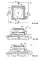
- FIG. 7is a schematic diagram showing an example of an acoustic coupler 300 in accordance with a second embodiment of the invention.
- FIG. 8Ais a plan view showing a practical example of acoustic coupler 300 and
- FIGS. 8B and 8Care cross-sectional views along section lines 8 B- 8 B and 8 C- 8 C, respectively, shown in FIG. 8A .
- the same reference numeralsare used to denote the elements of acoustic coupler 300 in FIG. 7 and in FIGS. 8A-8C .
- Acoustic coupler 300comprises an insulated stacked bulk acoustic resonator (IDSBAR) 306 in accordance with a second IDSBAR embodiment.
- IDSBARinsulated stacked bulk acoustic resonator
- an IDSBAR in accordance with the second IDSBAR embodimenthas a first half-wave acoustically-resonant electrical insulator, a single acoustic decoupler and a second half-wave acoustically-resonant electrical insulator located between its constituent FBARs.
- IDSBAR 306 in accordance with the second IDSBAR embodimentgives acoustic coupler 300 a substantially greater breakdown voltage than acoustic coupler 100 described above with reference to FIG. 2 and acoustic coupler 200 described above with reference to FIGS.
- acoustic coupler 300additionally comprises inputs 26 , 28 , outputs 32 , 34 , an electrical circuit 140 that connects IDSBAR 306 to inputs 26 , 28 and an electrical circuit 141 that connects IDSBAR 306 to outputs 32 , 34 .
- acoustic coupler 300When used as electrically-isolating acoustic coupler 16 in acoustic galvanic isolator 10 shown in FIG. 1 , acoustic coupler 300 acoustically couples modulated electrical signal S M from inputs 26 , 28 to outputs 32 , 34 while providing electrical isolation between inputs 26 , 28 and outputs 32 , 34 .
- acoustic coupler 300effectively galvanically isolates output terminals 36 , 38 from input terminals 22 , 24 , and allows the output terminals to differ in voltage from the input terminals by a voltage up to its specified breakdown voltage.
- IDSBAR 306shown in FIG. 7 comprises a lower film bulk acoustic resonator (FBAR) 110 , an upper film bulk acoustic resonator 120 stacked on FBAR 110 and, located in order between lower FBAR 110 and upper FBAR 120 , a first half-wave acoustically-resonant electrical insulator 316 , acoustic decoupler 130 and a second half-wave acoustically-resonant electrical insulator 326 .
- FBARlower film bulk acoustic resonator
- half-wave acoustically-resonant electrical insulatorsprovide additional electrical insulation between inputs 26 , 28 and outputs 32 , 34 without impairing the signal integrity of the modulated electrical signal S M acoustically coupled from inputs 26 , 28 to outputs 32 , 34 .
- half-wave acoustically-resonant electrical insulators 316 , 326are two in number and are twice as thick as acoustically-resonant electrical insulator 216 described above with reference to FIGS. 3 and 5 A- 5 C and therefore collectively provide approximately four times the electrical isolation provided by quarter-wave acoustically-resonant electrical insulator 216 .
- acoustic coupler 300has a greater breakdown voltage between inputs 26 , 28 and outputs 32 , 34 than otherwise similar embodiments of acoustic coupler 200 described above with reference to FIGS. 3 and 5 A- 5 C.
- IDSBAR 306comprises lower film bulk acoustic resonator (FBAR) 110 , upper film bulk acoustic resonator 120 stacked on FBAR 110 and, between lower FBAR 110 and upper FBAR 120 , in order, half-wave acoustically-resonant electrical insulator 316 , acoustic decoupler 130 and half-wave acoustically-resonant electrical insulator 326 .
- FBARfilm bulk acoustic resonator
- 120stacked on FBAR 110 and, between lower FBAR 110 and upper FBAR 120 , in order, half-wave acoustically-resonant electrical insulator 316 , acoustic decoupler 130 and half-wave acoustically-resonant electrical insulator 326 .
- IDSBAR 306comprise an even number (2n) of half-wave acoustically-resonant electrical insulators interleaved with a corresponding number (2n ⁇ 1) of acoustic decouplers located between the respective FBARs.
- FBARs 110 and 120acoustic decoupler 130 , electrical circuits 140 and 141 and substrate 102 are described above with reference to FIGS. 3 and 5 A- 5 C and will not be described again here.
- the exemplary embodiments of acoustic decoupler 130 described above with reference to FIGS. 6A and 6Bmay be used to provide acoustic decoupler 130 .
- Half-wave acoustically-resonant electrical insulator 316will now be described. The following description also applies to half-wave acoustically-resonant electrical insulator 326 , so half-wave acoustically-resonant electrical insulator 326 will not be individually described.
- Acoustically-resonant electrical insulator 316is a half-wave layer of electrically-insulating material that is nominally matched in acoustic impedance to FBARs 110 and 120 .
- Embodiments in which half-wave acoustically-resonant electrical insulator 316 is a one half-wave layertypically couple modulated electrical signal S M from inputs 26 , 28 to outputs 32 , 34 with optimum signal integrity.
- half-wave acoustically-resonant electrical insulator 316 and half-wave acoustically-resonant electrical insulator 326are acoustically transparent.
- Half-wave acoustically-resonant electrical insulator 316couples the acoustic signal generated by FBAR 110 to acoustic decoupler 130 and half-wave acoustically-resonant electrical insulator 326 couples the acoustic signal transmitted by acoustic decoupler 130 to FBAR 120 .
- IDSBAR 306has signal coupling characteristics similar to those of DSBAR 106 described above with reference to: FIGS. 3 and 5 A- 5 C.
- acoustic coupler 300effectively couples the modulated electrical signal S M from inputs 26 , 28 to outputs 32 , 34 but electrically isolates outputs 32 , 34 from inputs 26 , 28 .
- the materials described above with reference to FIGS. 3 and 5 A- 5 C as being suitable for use as quarter-wave acoustically-resonant electrical insulator 216are suitable for use as half-wave acoustically-resonant electrical insulators 316 and 326 .
- the materials of half-wave acoustically-resonant electrical insulators 316 and 326will therefore not be further described.
- Half-wave acoustically-resonant electrical insulator 316is twice as thick as above-described quarter-wave acoustically-resonant electrical insulator 216 , and two half-wave acoustically-resonant electrical insulators 316 and 326 separate FBAR 120 from FBAR 110 .
- a given voltage between inputs 26 , 28 and outputs 32 , 34produces a much lower electric field when applied across half-wave acoustically-resonant electrical insulators 316 and 326 and acoustic decoupler 130 than when applied across acoustic decoupler 130 in the embodiment of acoustic coupler 100 shown in FIG.
- acoustic coupler 300typically has a substantially greater breakdown voltage than acoustic coupler 100 shown in FIG. 2 and than acoustic coupler 200 shown in FIG. 3 .
- Thousands of acoustic galvanic isolators similar to acoustic galvanic isolator 10are fabricated at a time by wafer-scale fabrication. Such wafer-scale fabrication makes the acoustic galvanic isolators inexpensive to fabricate.
- the waferis selectively etched to define a cavity in the location of the electrically-isolating acoustic coupler 16 of each acoustic galvanic isolator to be fabricated on the wafer.
- the cavitiesare filled with sacrificial material and the surface of the wafer is planarized.
- the local oscillator 12 , modulator 14 and demodulator 18 of each acoustic galvanic isolator to be fabricated on the waferare fabricated in and on the surface of the wafer using conventional semiconductor fabrication processing.
- the fabricated circuit elementsare then covered with a protective layer.
- Exemplary materials for the protective layerare aluminum nitride and silicon nitride.
- Embodiments of acoustic coupler 200 described above with reference to FIGS. 5A-5Care then fabricated by sequentially depositing and patterning the following layers: a first layer of electrode material, a first layer of piezoelectric material, a second layer of electrode material, a first layer of acoustic decoupling material or the layers of a first acoustic Bragg structure, a quarter-wave layer of electrically-insulating material, a second layer of acoustic decoupling material, a third layer of electrode material, a second layer of piezoelectric material and a fourth layer of electrode material.
- These layersform the IDSBAR and the electrical circuits of each acoustic coupler.
- the electrical circuitsadditionally connect the ISBAR to exposed connection points on modulator 14 and demodulator 18 .
- Embodiments of acoustic coupler 300 described above with reference to FIGS. 8A-8Care fabricated by sequentially depositing and patterning the following layers: a first layer of electrode material, a first layer of piezoelectric material, a second layer of electrode material, a first half-wave layer of electrically-insulating material, a layer of acoustic decoupling material or the layers of an acoustic Bragg structure, a second half-wave layer of electrically-insulating material, a third layer of electrode material, a second layer of piezoelectric material and a fourth layer of electrode material.
- These layersform the IDSBAR and the electrical circuits of each acoustic coupler.
- the electrical circuitsadditionally connect the ISBAR to exposed connection points on modulator 14 and demodulator 18 are each deposited and patterned.
- the sacrificial materialis removed to leave each constituent IDSBAR over its respective cavity. Access holes (not shown) provide access to the sacrificial material to facilitate removal.
- the protective materialis then removed from the fabricated circuit elements.
- the substrateis then divided into individual acoustic galvanic isolators each similar to acoustic galvanic isolator 10 .
- An exemplary process that can be used to fabricate a DSBARis described in more detail in United States patent application publication no. 2005 0140 466, assigned to the assignee of this disclosure and incorporated by reference, and can be adapted to fabricate IDSBARs of the acoustic galvanic isolators described above.
- acoustic couplers 200 or 300are fabricated on a different wafer from that on which local oscillators 12 , modulators 14 and demodulators 18 are fabricated.
- the acoustic galvanic isolatorsmay be made by using a wafer bonding process to join the respective wafers to form a structure similar to that described by John D. Larson III et al. with reference to FIGS. 8A-8E of United States patent application publication No. 2005 0 093 659, assigned to the assignee of this disclosure and incorporated by reference.
- local oscillators 12 , modulators 14 and acoustic couplers 200 or 300are fabricated on one wafer and corresponding demodulators 18 are fabricated on the other wafer. The wafers are then bonded together as just described to form the acoustic galvanic isolators.
- the local oscillators 12 and modulators 14are fabricated on one wafer and the acoustic couplers 200 or 300 and demodulators 18 are fabricated on the other wafer. The wafers are then bonded together as just described to form the acoustic galvanic isolators.
- acoustic galvanic isolatorsare specified to have a large breakdown voltage between input terminals 22 , 24 and output terminals 36 , 38 .
- multiple input circuitseach comprising an instance of local oscillator 12 and an instance of modulator 14 and multiple output circuits each comprising an instance of demodulator 18 are fabricated in and on a semiconductor wafer.
- the waferis then singulated into individual semiconductor chips each embodying a single input circuit or a single output circuit.
- the electrically-isolating acoustic coupler 16 of each acoustic galvanic isolatoris fabricated suspended over a cavity defined in a ceramic wafer having conductive traces located on its major surface.
- one semiconductor chip embodying an input circuit and one semiconductor chip embodying an output circuitare mounted on the ceramic wafer in electrical contact with the conductive traces.
- the semiconductor chipsmay be mounted on the ceramic wafer by ball bonding or flip-chip bonding. Ceramic wafers with attached semiconductor chips can also be used in the above-described two wafer structure.
- the material of electrodes 112 , 114 , 122 and 124is molybdenum.
- Each of the electrodeshas a thickness of about 300 nm and is pentagonal in shape with an area of about 12,000 square ⁇ m. A different area gives a different characteristic impedance.
- the non-parallel sides of the electrodesminimize lateral modes in FBARs 110 and 120 as described by Larson III et al. in U.S. Pat. No. 6,215,375, assigned to the assignee of this disclosure and incorporated by reference.
- electrodes 112 , 114 , 122 , and 24are patterned such that, in respective planes parallel to the major surface of the wafer, electrodes 112 and 114 of FBAR 110 have the same shape, size, orientation and position, and electrodes 122 and 124 of FBAR 120 have the same shape, size, orientation and position.
- electrodes 114 and 122additionally have the same shape, size, orientation and position.
- Alternative electrode materialsinclude such metals as tungsten, niobium and titanium.
- the electrodesmay have a multi-layer structure.
- piezoelectric elements 116 and 126are aluminum nitride. Each piezoelectric element has a thickness of about 1.4 ⁇ m.
- Alternative piezoelectric materialsinclude zinc oxide, cadmium sulfide and poled ferroelectric materials such as perovskite ferroelectric materials, including lead zirconium titanate (PZT), lead metaniobate and barium titanate.
- the acoustic decoupling material constituting acoustic decoupling layer 131 in the embodiment of acoustic decoupler 130 shown in FIG. 6Ais polyimide, parylene or a crosslinked polyphenylene polymer, as described above.
- a one quarter-wave layer of polyimideis about 100 nm thick whereas a one quarter-wave layer of crosslinked polyphenylene polymer is about 190 nm thick.
- the acoustic decoupling layer 131may have a thickness of three, five or more times the above-specified one quarter-wave layer thickness. Suitable materials for use in embodiments in which acoustic decoupler 130 is embodied as an acoustic Bragg structure are described above.
- acoustically-resonant electrical insulator 216is aluminum nitride. Acoustically-resonant electrical insulator 216 has a thickness of about 1.4 ⁇ m. Alternative materials include aluminum oxide (Al 2 O 3 ) and non-piezoelectric aluminum nitride (AlN). Exemplary acoustic decoupling material for the second acoustic decoupling layer providing the embodiments of second acoustic decoupler 230 include polyimide, parylene or a crosslinked polyphenylene polymer, as described above.
- the material of half-wave acoustically-resonant electrical insulators 316 and 326is aluminum nitride.
- Each half-wave acoustically-resonant electrical insulatorhas a thickness of about 2.8 ⁇ m.
- Alternative materialsinclude aluminum oxide (Al 2 O 3 ) and non-piezoelectric aluminum nitride (AlN).
- inputs 26 , 28are connected to FBAR 110 and outputs 32 , 34 are connected to FBAR 120 .
- the direction in which the acoustic signal flowsis reversed, and outputs 32 , 34 are connected to FBAR 110 and inputs 26 , 28 are connected to FBAR 120 .
- FIG. 9is a flow chart showing an example of a method 170 in accordance with an embodiment of the invention for galvanically isolating an information signal.
- an electrically-isolating acoustic coupleris provided.
- the electrically-isolating acoustic couplercomprises no more than one decoupled stacked bulk acoustic resonator comprising an acoustically-resonant electrical insulator.
- a carrier signalis provided.
- the carrier signalis modulated with the information signal to form a modulated electrical signal.
- the modulated electrical signalis acoustically coupled through the electrically-isolating acoustic coupler.
- the information signalis recovered from the modulated electrical signal acoustically coupled though the acoustic coupler.
Landscapes
- Physics & Mathematics (AREA)
- Acoustics & Sound (AREA)
- Chemical & Material Sciences (AREA)
- Crystallography & Structural Chemistry (AREA)
- Engineering & Computer Science (AREA)
- Computer Networks & Wireless Communication (AREA)
- Signal Processing (AREA)
- Piezo-Electric Or Mechanical Vibrators, Or Delay Or Filter Circuits (AREA)
- Networks Using Active Elements (AREA)
Abstract
Description
t≈(2m+1)λn/4 (1)
where λnis the wavelength of the above-mentioned acoustic signal in the acoustically-transmissive material and m is an integer equal to or greater than zero. The thickness of a quarter-wave layer may differ from the nominal thickness by approximately ±10% of λn/4. A thickness outside this tolerance range can be used with some degradation in performance, but the thickness of a quarter-wave layer always differs significantly from an integral multiple of λn/2.
t≈nλn/2 (2)
where n is an integer greater than zero. The thickness of a half-wave layer may differ from the nominal thickness by approximately ±10% of λn/2. A thickness outside this tolerance range can be used with some degradation in performance, but the thickness of a half-wave layer always differs significantly from an odd integral multiple of λn/4. The term half-wave layer may be preceded with a number to denote a layer having a thickness equal to a specific number of half wavelengths of the above-mentioned acoustic signal in the material of the layer.
Claims (22)
Priority Applications (5)
| Application Number | Priority Date | Filing Date | Title |
|---|---|---|---|
| US11/253,508US7425787B2 (en) | 2005-10-18 | 2005-10-18 | Acoustic galvanic isolator incorporating single insulated decoupled stacked bulk acoustic resonator with acoustically-resonant electrical insulator |
| DE102006048632ADE102006048632B4 (en) | 2005-10-18 | 2006-10-13 | Acoustic galvanic isolator comprising a single, isolated, decoupled, stacked, bulk acoustic resonator with acoustically resonant electrical insulator |
| GB0620657AGB2431534A (en) | 2005-10-18 | 2006-10-17 | Electrically-insulating DSBAR acts as acoustically-coupled galvanic isolator |
| CN2006101400717ACN1953434B (en) | 2005-10-18 | 2006-10-18 | Acoustic galvanic isolator, and method of electrical isolation to information signal |
| JP2006283624AJP5189752B2 (en) | 2005-10-18 | 2006-10-18 | Acoustic galvanic separation device incorporating a single insulation decoupled stacked bulk acoustic resonator with an acoustic resonant electrical insulator |
Applications Claiming Priority (1)
| Application Number | Priority Date | Filing Date | Title |
|---|---|---|---|
| US11/253,508US7425787B2 (en) | 2005-10-18 | 2005-10-18 | Acoustic galvanic isolator incorporating single insulated decoupled stacked bulk acoustic resonator with acoustically-resonant electrical insulator |
Publications (2)
| Publication Number | Publication Date |
|---|---|
| US20070085447A1 US20070085447A1 (en) | 2007-04-19 |
| US7425787B2true US7425787B2 (en) | 2008-09-16 |
Family
ID=37507922
Family Applications (1)
| Application Number | Title | Priority Date | Filing Date |
|---|---|---|---|
| US11/253,508Expired - LifetimeUS7425787B2 (en) | 2005-10-18 | 2005-10-18 | Acoustic galvanic isolator incorporating single insulated decoupled stacked bulk acoustic resonator with acoustically-resonant electrical insulator |
Country Status (5)
| Country | Link |
|---|---|
| US (1) | US7425787B2 (en) |
| JP (1) | JP5189752B2 (en) |
| CN (1) | CN1953434B (en) |
| DE (1) | DE102006048632B4 (en) |
| GB (1) | GB2431534A (en) |
Cited By (52)
| Publication number | Priority date | Publication date | Assignee | Title |
|---|---|---|---|---|
| US20070063622A1 (en)* | 2005-09-09 | 2007-03-22 | Rudy Richard C | Adjusted frequency temperature coefficient resonator |
| US20070228876A1 (en)* | 2006-03-31 | 2007-10-04 | Chien-Min Sung | Diamond Frequency Control Devices and Associated Methods |
| US20080180206A1 (en)* | 2006-08-28 | 2008-07-31 | Avago Technologies Ecbu (Singapore) Pte.Ltd. | Coil Transducer with Reduced Arcing and Improved High Voltage Breakdown Performance Characteristics |
| US20080179963A1 (en)* | 2006-08-28 | 2008-07-31 | Avago Technologies Ecbu (Singapore) Pte. Ltd. | Galvanic Isolators and Coil Transducers |
| US20090076329A1 (en)* | 2007-09-17 | 2009-03-19 | Wei Su | Disposable Stereoscopic Endoscope System |
| US20090146531A1 (en)* | 2003-03-07 | 2009-06-11 | Ruby Richard C | Manufacturing Process For Thin Film Bulk Acoustic Resonator (FBAR) Filters |
| US20090153283A1 (en)* | 2007-05-10 | 2009-06-18 | Avago Technologies Ecbu Ip(Singapore) Pte. Ltd. | Miniature transformers adapted for use in galvanic isolators and the like |
| US7561009B2 (en) | 2005-11-30 | 2009-07-14 | Avago Technologies General Ip (Singapore) Pte. Ltd. | Film bulk acoustic resonator (FBAR) devices with temperature compensation |
| US20090243782A1 (en)* | 2006-08-28 | 2009-10-01 | Avago Technologies Ecbu (Singapore) Pte. Ltd. | High Voltage Hold-Off Coil Transducer |
| US20090243783A1 (en)* | 2006-08-28 | 2009-10-01 | Avago Technologies Ecbu (Singapore) Pte. Ltd. | Minimizing Electromagnetic Interference in Coil Transducers |
| US20100020448A1 (en)* | 2006-08-28 | 2010-01-28 | Avago Technologies Ecbu Ip (Singapore) Pte. Ltd. | Galvanic isolator |
| US7675390B2 (en)* | 2005-10-18 | 2010-03-09 | Avago Technologies Wireless Ip (Singapore) Pte. Ltd. | Acoustic galvanic isolator incorporating single decoupled stacked bulk acoustic resonator |
| US7714684B2 (en) | 2004-10-01 | 2010-05-11 | Avago Technologies Wireless Ip (Singapore) Pte. Ltd. | Acoustic resonator performance enhancement using alternating frame structure |
| US7732977B2 (en) | 2008-04-30 | 2010-06-08 | Avago Technologies Wireless Ip (Singapore) | Transceiver circuit for film bulk acoustic resonator (FBAR) transducers |
| US7737807B2 (en)* | 2005-10-18 | 2010-06-15 | Avago Technologies Wireless Ip (Singapore) Pte. Ltd. | Acoustic galvanic isolator incorporating series-connected decoupled stacked bulk acoustic resonators |
| US7746677B2 (en) | 2006-03-09 | 2010-06-29 | Avago Technologies Wireless Ip (Singapore) Pte. Ltd. | AC-DC converter circuit and power supply |
| US20100176660A1 (en)* | 2006-08-28 | 2010-07-15 | Avago Technologies General IP (Singpore) Pte. Ltd. | Galvanic isolator |
| US20100188182A1 (en)* | 2006-08-28 | 2010-07-29 | Avago Technologies Ecbu (Singapore) Pte.Ltd. | Narrowbody Coil Isolator |
| US7791434B2 (en) | 2004-12-22 | 2010-09-07 | Avago Technologies Wireless Ip (Singapore) Pte. Ltd. | Acoustic resonator performance enhancement using selective metal etch and having a trench in the piezoelectric |
| US7791435B2 (en) | 2007-09-28 | 2010-09-07 | Avago Technologies Wireless Ip (Singapore) Pte. Ltd. | Single stack coupled resonators having differential output |
| US7852644B2 (en) | 2005-10-31 | 2010-12-14 | Avago Technologies General Ip (Singapore) Pte. Ltd. | AC-DC power converter |
| US7855618B2 (en) | 2008-04-30 | 2010-12-21 | Avago Technologies Wireless Ip (Singapore) Pte. Ltd. | Bulk acoustic resonator electrical impedance transformers |
| US20100328902A1 (en)* | 2009-06-30 | 2010-12-30 | Avago Technologies Ecbu Ip (Singapore) Pte. Ltd. | Coil Transducer Isolator Packages |
| US20110204996A1 (en)* | 2010-02-23 | 2011-08-25 | Avago Technologies Wireless Ip (Singapore) Pte. Ltd. | Acoustic coupling layer for coupled resonator filters and method of fabricating acoustic coupling layer |
| US8080854B2 (en) | 2006-03-10 | 2011-12-20 | Avago Technologies General Ip (Singapore) Pte. Ltd. | Electronic device on substrate with cavity and mitigated parasitic leakage path |
| US8143082B2 (en) | 2004-12-15 | 2012-03-27 | Avago Technologies Wireless Ip (Singapore) Pte. Ltd. | Wafer bonding of micro-electro mechanical systems to active circuitry |
| US20120104900A1 (en)* | 2010-11-01 | 2012-05-03 | Taiyo Yuden Co., Ltd. | Acoustic wave device |
| US8193877B2 (en) | 2009-11-30 | 2012-06-05 | Avago Technologies Wireless Ip (Singapore) Pte. Ltd. | Duplexer with negative phase shifting circuit |
| US8230562B2 (en) | 2005-04-06 | 2012-07-31 | Avago Technologies Wireless Ip (Singapore) Pte. Ltd. | Method of fabricating an acoustic resonator comprising a filled recessed region |
| US8248185B2 (en) | 2009-06-24 | 2012-08-21 | Avago Technologies Wireless Ip (Singapore) Pte. Ltd. | Acoustic resonator structure comprising a bridge |
| US8258911B2 (en) | 2008-03-31 | 2012-09-04 | Avago Technologies ECBU IP (Singapor) Pte. Ltd. | Compact power transformer components, devices, systems and methods |
| US8291559B2 (en)* | 2009-02-24 | 2012-10-23 | Epcos Ag | Process for adapting resonance frequency of a BAW resonator |
| US8350445B1 (en) | 2011-06-16 | 2013-01-08 | Avago Technologies Wireless Ip (Singapore) Pte. Ltd. | Bulk acoustic resonator comprising non-piezoelectric layer and bridge |
| US8427844B2 (en) | 2006-08-28 | 2013-04-23 | Avago Technologies Ecbu Ip (Singapore) Pte. Ltd. | Widebody coil isolators |
| US8575820B2 (en) | 2011-03-29 | 2013-11-05 | Avago Technologies General Ip (Singapore) Pte. Ltd. | Stacked bulk acoustic resonator |
| US8796904B2 (en) | 2011-10-31 | 2014-08-05 | Avago Technologies General Ip (Singapore) Pte. Ltd. | Bulk acoustic resonator comprising piezoelectric layer and inverse piezoelectric layer |
| US8902023B2 (en) | 2009-06-24 | 2014-12-02 | Avago Technologies General Ip (Singapore) Pte. Ltd. | Acoustic resonator structure having an electrode with a cantilevered portion |
| US8922302B2 (en) | 2011-08-24 | 2014-12-30 | Avago Technologies General Ip (Singapore) Pte. Ltd. | Acoustic resonator formed on a pedestal |
| US8962443B2 (en) | 2011-01-31 | 2015-02-24 | Avago Technologies General Ip (Singapore) Pte. Ltd. | Semiconductor device having an airbridge and method of fabricating the same |
| US8981876B2 (en) | 2004-11-15 | 2015-03-17 | Avago Technologies General Ip (Singapore) Pte. Ltd. | Piezoelectric resonator structures and electrical filters having frame elements |
| US9048812B2 (en) | 2011-02-28 | 2015-06-02 | Avago Technologies General Ip (Singapore) Pte. Ltd. | Bulk acoustic wave resonator comprising bridge formed within piezoelectric layer |
| US9083302B2 (en) | 2011-02-28 | 2015-07-14 | Avago Technologies General Ip (Singapore) Pte. Ltd. | Stacked bulk acoustic resonator comprising a bridge and an acoustic reflector along a perimeter of the resonator |
| US9136818B2 (en) | 2011-02-28 | 2015-09-15 | Avago Technologies General Ip (Singapore) Pte. Ltd. | Stacked acoustic resonator comprising a bridge |
| US9148117B2 (en) | 2011-02-28 | 2015-09-29 | Avago Technologies General Ip (Singapore) Pte. Ltd. | Coupled resonator filter comprising a bridge and frame elements |
| US9154112B2 (en) | 2011-02-28 | 2015-10-06 | Avago Technologies General Ip (Singapore) Pte. Ltd. | Coupled resonator filter comprising a bridge |
| US9203374B2 (en) | 2011-02-28 | 2015-12-01 | Avago Technologies General Ip (Singapore) Pte. Ltd. | Film bulk acoustic resonator comprising a bridge |
| US9243316B2 (en) | 2010-01-22 | 2016-01-26 | Avago Technologies General Ip (Singapore) Pte. Ltd. | Method of fabricating piezoelectric material with selected c-axis orientation |
| US9425764B2 (en) | 2012-10-25 | 2016-08-23 | Avago Technologies General Ip (Singapore) Pte. Ltd. | Accoustic resonator having composite electrodes with integrated lateral features |
| US9444426B2 (en) | 2012-10-25 | 2016-09-13 | Avago Technologies General Ip (Singapore) Pte. Ltd. | Accoustic resonator having integrated lateral feature and temperature compensation feature |
| US9490771B2 (en) | 2012-10-29 | 2016-11-08 | Avago Technologies General Ip (Singapore) Pte. Ltd. | Acoustic resonator comprising collar and frame |
| US9490418B2 (en) | 2011-03-29 | 2016-11-08 | Avago Technologies General Ip (Singapore) Pte. Ltd. | Acoustic resonator comprising collar and acoustic reflector with temperature compensating layer |
| US10574184B2 (en)* | 2018-05-01 | 2020-02-25 | Texas Instruments Incorporated | Stacked-die bulk acoustic wave oscillator package |
Families Citing this family (32)
| Publication number | Priority date | Publication date | Assignee | Title |
|---|---|---|---|---|
| US6946928B2 (en)* | 2003-10-30 | 2005-09-20 | Agilent Technologies, Inc. | Thin-film acoustically-coupled transformer |
| US7362198B2 (en) | 2003-10-30 | 2008-04-22 | Avago Technologies Wireless Ip (Singapore) Pte. Ltd | Pass bandwidth control in decoupled stacked bulk acoustic resonator devices |
| EP1528677B1 (en) | 2003-10-30 | 2006-05-10 | Agilent Technologies, Inc. | Film acoustically-coupled transformer with two reverse c-axis piezoelectric elements |
| US7358831B2 (en)* | 2003-10-30 | 2008-04-15 | Avago Technologies Wireless Ip (Singapore) Pte. Ltd. | Film bulk acoustic resonator (FBAR) devices with simplified packaging |
| US7019605B2 (en)* | 2003-10-30 | 2006-03-28 | Larson Iii John D | Stacked bulk acoustic resonator band-pass filter with controllable pass bandwidth |
| US7615833B2 (en) | 2004-07-13 | 2009-11-10 | Avago Technologies Wireless Ip (Singapore) Pte. Ltd. | Film bulk acoustic resonator package and method of fabricating same |
| US7427819B2 (en)* | 2005-03-04 | 2008-09-23 | Avago Wireless Ip Pte Ltd | Film-bulk acoustic wave resonator with motion plate and method |
| US7436269B2 (en)* | 2005-04-18 | 2008-10-14 | Avago Technologies Wireless Ip (Singapore) Pte. Ltd. | Acoustically coupled resonators and method of making the same |
| US7934884B2 (en)* | 2005-04-27 | 2011-05-03 | Lockhart Industries, Inc. | Ring binder cover |
| US7391286B2 (en)* | 2005-10-06 | 2008-06-24 | Avago Wireless Ip Pte Ltd | Impedance matching and parasitic capacitor resonance of FBAR resonators and coupled filters |
| US20070085632A1 (en)* | 2005-10-18 | 2007-04-19 | Larson John D Iii | Acoustic galvanic isolator |
| US7423503B2 (en)* | 2005-10-18 | 2008-09-09 | Avago Technologies Wireless Ip (Singapore) Pte. Ltd. | Acoustic galvanic isolator incorporating film acoustically-coupled transformer |
| US7425787B2 (en) | 2005-10-18 | 2008-09-16 | Avago Technologies Wireless Ip (Singapore) Pte. Ltd. | Acoustic galvanic isolator incorporating single insulated decoupled stacked bulk acoustic resonator with acoustically-resonant electrical insulator |
| US7612636B2 (en)* | 2006-01-30 | 2009-11-03 | Avago Technologies Wireless Ip (Singapore) Pte. Ltd. | Impedance transforming bulk acoustic wave baluns |
| US7629865B2 (en) | 2006-05-31 | 2009-12-08 | Avago Technologies Wireless Ip (Singapore) Pte. Ltd. | Piezoelectric resonator structures and electrical filters |
| US7508286B2 (en)* | 2006-09-28 | 2009-03-24 | Avago Technologies Wireless Ip (Singapore) Pte. Ltd. | HBAR oscillator and method of manufacture |
| US20080202239A1 (en)* | 2007-02-28 | 2008-08-28 | Fazzio R Shane | Piezoelectric acceleration sensor |
| US20090079514A1 (en)* | 2007-09-24 | 2009-03-26 | Tiberiu Jamneala | Hybrid acoustic resonator-based filters |
| FR2954014B1 (en)* | 2009-12-11 | 2012-08-24 | St Microelectronics Tours Sas | GALVANIC INSULATION DEVICE |
| KR101136519B1 (en)* | 2010-03-09 | 2012-04-17 | (주)파트론 | Intergrated coupler-circulator and power amplifier compring the same |
| US9401692B2 (en) | 2012-10-29 | 2016-07-26 | Avago Technologies General Ip (Singapore) Pte. Ltd. | Acoustic resonator having collar structure |
| US9608592B2 (en)* | 2014-01-21 | 2017-03-28 | Avago Technologies General Ip (Singapore) Pte. Ltd. | Film bulk acoustic wave resonator (FBAR) having stress-relief |
| US9385684B2 (en) | 2012-10-23 | 2016-07-05 | Avago Technologies General Ip (Singapore) Pte. Ltd. | Acoustic resonator having guard ring |
| JP6337461B2 (en)* | 2013-12-17 | 2018-06-06 | 富士通株式会社 | Wireless communication apparatus and handover control method in base station apparatus |
| KR20160148556A (en)* | 2014-04-01 | 2016-12-26 | 큐오알테크, 인크. | Galvanic isolated ceramic based voltage sensors |
| GB201707440D0 (en)* | 2017-05-09 | 2017-06-21 | Cambridge Entpr Ltd | Method for operation of resonator |
| CN107241077B (en)* | 2017-05-12 | 2020-12-29 | 电子科技大学 | Piezoelectric thin-film bulk acoustic wave resonator and method of making the same |
| WO2018222504A2 (en) | 2017-06-02 | 2018-12-06 | Lawrence Livermore National Security, Llc | Innovative solutions for improving laser damage performance of multi-layer dielectric gratings |
| US11835743B2 (en) | 2017-06-02 | 2023-12-05 | Lawrence Livermore National Security, Llc | Innovative solutions to improve laser damage thresholds of optical structures |
| FR3070898A1 (en)* | 2017-09-13 | 2019-03-15 | Compagnie Generale Des Etablissements Michelin | TIRE TREAD BAND COMPRISING HIDDEN CHANNELS. |
| TWI792000B (en)* | 2019-06-23 | 2023-02-11 | 美商羅門哈斯電子材料有限公司 | Gas sensors and methods of sensing a gas-phase analyte |
| WO2022230723A1 (en)* | 2021-04-30 | 2022-11-03 | 株式会社村田製作所 | Elastic wave device |
Citations (216)
| Publication number | Priority date | Publication date | Assignee | Title |
|---|---|---|---|---|
| US3174122A (en) | 1960-12-12 | 1965-03-16 | Sonus Corp | Frequency selective amplifier |
| US3189851A (en) | 1962-06-04 | 1965-06-15 | Sonus Corp | Piezoelectric filter |
| US3321648A (en) | 1964-06-04 | 1967-05-23 | Sonus Corp | Piezoelectric filter element |
| US3422371A (en) | 1967-07-24 | 1969-01-14 | Sanders Associates Inc | Thin film piezoelectric oscillator |
| GB1207974A (en) | 1966-11-17 | 1970-10-07 | Clevite Corp | Frequency selective apparatus including a piezoelectric device |
| US3582839A (en) | 1968-06-06 | 1971-06-01 | Clevite Corp | Composite coupled-mode filter |
| US3607761A (en) | 1968-12-09 | 1971-09-21 | Continental Oil Co | Soap bars containing salts of fatty acids derived from the guerbet reaction |
| US3610969A (en) | 1970-02-06 | 1971-10-05 | Mallory & Co Inc P R | Monolithic piezoelectric resonator for use as filter or transformer |
| US3826931A (en) | 1967-10-26 | 1974-07-30 | Hewlett Packard Co | Dual crystal resonator apparatus |
| US3845402A (en) | 1973-02-15 | 1974-10-29 | Edmac Ass Inc | Sonobuoy receiver system, floating coupler |
| US4084217A (en) | 1977-04-19 | 1978-04-11 | Bbc Brown, Boveri & Company, Limited | Alternating-current fed power supply |
| US4172277A (en) | 1977-02-14 | 1979-10-23 | Compagnie Internationale Pour L'informatique Cii-Honeywell Bull (Societe Anonyme) | Chopping control system for a converter in a DC electrical power supply |
| US4272742A (en) | 1978-09-22 | 1981-06-09 | The Secretary Of State For Defence In Her Britannic Majesty's Government Of The United Kingdom Of Great Britain And Northern Ireland | Acoustic wave devices with temperature stabilization |
| US4281299A (en) | 1979-11-23 | 1981-07-28 | Honeywell Inc. | Signal isolator |
| US4320365A (en) | 1980-11-03 | 1982-03-16 | United Technologies Corporation | Fundamental, longitudinal, thickness mode bulk wave resonator |
| US4355408A (en) | 1980-02-13 | 1982-10-19 | International Computers Limited | System for extracting timing information from a digital waveform |
| US4456850A (en) | 1982-02-09 | 1984-06-26 | Nippon Electric Co., Ltd. | Piezoelectric composite thin film resonator |
| US4529904A (en) | 1983-03-16 | 1985-07-16 | International Standard Electric Corporation | Piezo-electric terminal station for communications system |
| US4625138A (en) | 1984-10-24 | 1986-11-25 | The United States Of America As Represented By The Secretary Of The Army | Piezoelectric microwave resonator using lateral excitation |
| JPS6154686B2 (en) | 1982-10-06 | 1986-11-25 | Hitachi Ltd | |
| US4640756A (en) | 1983-10-25 | 1987-02-03 | The United States Of America As Represented By The United States Department Of Energy | Method of making a piezoelectric shear wave resonator |
| US4719383A (en) | 1985-05-20 | 1988-01-12 | The United States Of America As Represented By The United States Department Of Energy | Piezoelectric shear wave resonator and method of making same |
| US4798990A (en) | 1986-09-11 | 1989-01-17 | Bengt Henoch | Device for transmitting electric energy to computers and data nets |
| US4836882A (en) | 1988-09-12 | 1989-06-06 | The United States Of America As Represented By The Secretary Of The Army | Method of making an acceleration hardened resonator |
| US4841429A (en) | 1988-03-24 | 1989-06-20 | Hughes Aircraft Company | Capacitive coupled power supplies |
| US4906840A (en) | 1988-01-27 | 1990-03-06 | The Board Of Trustees Of Leland Stanford Jr., University | Integrated scanning tunneling microscope |
| US5048036A (en) | 1989-09-18 | 1991-09-10 | Spectra Diode Laboratories, Inc. | Heterostructure laser with lattice mismatch |
| US5048038A (en) | 1990-01-25 | 1991-09-10 | The United States Of America As Represented By The United States Department Of Energy | Ion-implanted planar-buried-heterostructure diode laser |
| US5075641A (en) | 1990-12-04 | 1991-12-24 | Iowa State University Research Foundation, Inc. | High frequency oscillator comprising cointegrated thin film resonator and active device |
| US5118982A (en) | 1989-05-31 | 1992-06-02 | Nec Corporation | Thickness mode vibration piezoelectric transformer |
| US5162691A (en) | 1991-01-22 | 1992-11-10 | The United States Of America As Represented By The Secretary Of The Army | Cantilevered air-gap type thin film piezoelectric resonator |
| US5241209A (en) | 1990-07-24 | 1993-08-31 | Fujitsu Limited | Semi-conductor device having circuits on both sides of insulation layer and ultrasonic signal path between the circuits |
| US5241456A (en) | 1990-07-02 | 1993-08-31 | General Electric Company | Compact high density interconnect structure |
| US5294898A (en) | 1992-01-29 | 1994-03-15 | Motorola, Inc. | Wide bandwidth bandpass filter comprising parallel connected piezoelectric resonators |
| US5382930A (en) | 1992-12-21 | 1995-01-17 | Trw Inc. | Monolithic multipole filters made of thin film stacked crystal filters |
| US5384808A (en) | 1992-12-31 | 1995-01-24 | Apple Computer, Inc. | Method and apparatus for transmitting NRZ data signals across an isolation barrier disposed in an interface between adjacent devices on a bus |
| US5448014A (en) | 1993-01-27 | 1995-09-05 | Trw Inc. | Mass simultaneous sealing and electrical connection of electronic devices |
| US5465725A (en) | 1993-06-15 | 1995-11-14 | Hewlett Packard Company | Ultrasonic probe |
| EP0689254A1 (en) | 1994-06-23 | 1995-12-27 | Motorola, Inc. | Accoustic isolator |
| US5587620A (en) | 1993-12-21 | 1996-12-24 | Hewlett-Packard Company | Tunable thin film acoustic resonators and method for making the same |
| US5589858A (en) | 1990-05-22 | 1996-12-31 | Canon Kabushiki Kaisha | Information recording apparatus |
| US5594705A (en) | 1994-02-04 | 1997-01-14 | Dynamotive Canada Corporation | Acoustic transformer with non-piezoelectric core |
| US5671242A (en) | 1994-09-02 | 1997-09-23 | Mitsubishi Denki Kabushiki Kaisha | Strained quantum well structure |
| US5692279A (en) | 1995-08-17 | 1997-12-02 | Motorola | Method of making a monolithic thin film resonator lattice filter |
| US5705877A (en) | 1995-10-12 | 1998-01-06 | Nec Corporation | Piezoelectric transformer driving circuit |
| US5714917A (en) | 1996-10-02 | 1998-02-03 | Nokia Mobile Phones Limited | Device incorporating a tunable thin film bulk acoustic resonator for performing amplitude and phase modulation |
| WO1998016957A1 (en) | 1996-10-17 | 1998-04-23 | Nokia Mobile Phones Limited | A resonator having an acoustic mirror |
| US5853601A (en) | 1997-04-03 | 1998-12-29 | Northrop Grumman Corporation | Top-via etch technique for forming dielectric membranes |
| US5864261A (en) | 1994-05-23 | 1999-01-26 | Iowa State University Research Foundation | Multiple layer acoustical structures for thin-film resonator based circuits and systems |
| US5866969A (en) | 1996-10-24 | 1999-02-02 | Nec Corporation | Actuating circuit of piezoelectric transformer and actuating method thereof |
| US5872493A (en) | 1997-03-13 | 1999-02-16 | Nokia Mobile Phones, Ltd. | Bulk acoustic wave (BAW) filter having a top portion that includes a protective acoustic mirror |
| US5894184A (en) | 1996-08-01 | 1999-04-13 | Nec Corporation | Drive circuit for driving a piezoelectric transformer capable of decreasing heat developed from electronic parts composing an inverter circuit |
| US5894647A (en) | 1997-06-30 | 1999-04-20 | Tfr Technologies, Inc. | Method for fabricating piezoelectric resonators and product |
| US5910756A (en) | 1997-05-21 | 1999-06-08 | Nokia Mobile Phones Limited | Filters and duplexers utilizing thin film stacked crystal filter structures and thin film bulk acoustic wave resonators |
| US5932953A (en) | 1997-06-30 | 1999-08-03 | Iowa State University Research Foundation, Inc. | Method and system for detecting material using piezoelectric resonators |
| US5936150A (en)* | 1998-04-13 | 1999-08-10 | Rockwell Science Center, Llc | Thin film resonant chemical sensor with resonant acoustic isolator |
| US5953479A (en) | 1998-05-07 | 1999-09-14 | The United States Of America As Represented By The Secretary Of The Army | Tilted valance-band quantum well double heterostructures for single step active and passive optical waveguide device monolithic integration |
| US5982297A (en) | 1997-10-08 | 1999-11-09 | The Aerospace Corporation | Ultrasonic data communication system |
| US6040962A (en) | 1997-05-14 | 2000-03-21 | Tdk Corporation | Magnetoresistive element with conductive films and magnetic domain films overlapping a central active area |
| US6060818A (en) | 1998-06-02 | 2000-05-09 | Hewlett-Packard Company | SBAR structures and method of fabrication of SBAR.FBAR film processing techniques for the manufacturing of SBAR/BAR filters |
| US6087198A (en) | 1998-02-12 | 2000-07-11 | Texas Instruments Incorporated | Low cost packaging for thin-film resonators and thin-film resonator-based filters |
| US6107721A (en) | 1999-07-27 | 2000-08-22 | Tfr Technologies, Inc. | Piezoelectric resonators on a differentially offset reflector |
| US6111480A (en) | 1997-07-07 | 2000-08-29 | Murata Manfacturing Co., Ltd. | Piezoelectric resonator and method of adjusting resonant frequency thereof |
| US6124756A (en) | 1996-04-08 | 2000-09-26 | Texas Instruments Incorporated | Method and apparatus for galvanically isolating two integrated circuits from each other |
| US6150703A (en) | 1998-06-29 | 2000-11-21 | Trw Inc. | Lateral mode suppression in semiconductor bulk acoustic resonator (SBAR) devices using tapered electrodes, and electrodes edge damping materials |
| WO2001006647A1 (en) | 1999-07-19 | 2001-01-25 | Nokia Corporation | Resonator structure and a filter comprising such a resonator structure |
| US6187513B1 (en) | 1998-05-29 | 2001-02-13 | Sony Corporation | Process for forming mask pattern and process for producing thin film magnetic head |
| US6215375B1 (en) | 1999-03-30 | 2001-04-10 | Agilent Technologies, Inc. | Bulk acoustic wave resonator with improved lateral mode suppression |
| EP1096259A1 (en) | 1999-11-01 | 2001-05-02 | Samsung Electronics Co., Ltd. | High-vacuum packaged microgyroscope and method for manufacturing the same |
| US6228675B1 (en) | 1999-07-23 | 2001-05-08 | Agilent Technologies, Inc. | Microcap wafer-level package with vias |
| US6229247B1 (en) | 1998-11-09 | 2001-05-08 | Face International Corp. | Multi-layer piezoelectric electrical energy transfer device |
| US6252229B1 (en) | 1998-07-10 | 2001-06-26 | Boeing North American, Inc. | Sealed-cavity microstructure and microbolometer and associated fabrication methods |
| US6262600B1 (en) | 2000-02-14 | 2001-07-17 | Analog Devices, Inc. | Isolator for transmitting logic signals across an isolation barrier |
| US6262637B1 (en) | 1999-06-02 | 2001-07-17 | Agilent Technologies, Inc. | Duplexer incorporating thin-film bulk acoustic resonators (FBARs) |
| US6265246B1 (en) | 1999-07-23 | 2001-07-24 | Agilent Technologies, Inc. | Microcap wafer-level package |
| US6278342B1 (en) | 1998-12-30 | 2001-08-21 | Nokia Mobile Phones, Ltd. | Balanced filter structure utilizing bulk acoustic wave resonators having different areas |
| US6292336B1 (en) | 1999-09-30 | 2001-09-18 | Headway Technologies, Inc. | Giant magnetoresistive (GMR) sensor element with enhanced magnetoresistive (MR) coefficient |
| EP1047189A3 (en) | 1999-04-19 | 2001-09-19 | Murata Manufacturing Co., Ltd. | Piezoelectric resonator |
| US6307447B1 (en) | 1999-11-01 | 2001-10-23 | Agere Systems Guardian Corp. | Tuning mechanical resonators for electrical filter |
| WO2001099276A1 (en) | 2000-06-20 | 2001-12-27 | Koninklijke Philips Electronics N.V. | A bulk acoustic wave device |
| US20020000646A1 (en) | 2000-02-02 | 2002-01-03 | Raytheon Company, A Delware Corporation | Vacuum package fabrication of integrated circuit components |
| US20020030424A1 (en) | 1999-12-22 | 2002-03-14 | Toyo Communication Equipment Co., Ltd. | High frequency piezoelectric resonator |
| US6366006B1 (en) | 2000-12-15 | 2002-04-02 | Clark Davis Boyd | Composite piezoelectric transformer |
| US6377137B1 (en) | 2000-09-11 | 2002-04-23 | Agilent Technologies, Inc. | Acoustic resonator filter with reduced electromagnetic influence due to die substrate thickness |
| US6384697B1 (en) | 2000-05-08 | 2002-05-07 | Agilent Technologies, Inc. | Cavity spanning bottom electrode of a substrate-mounted bulk wave acoustic resonator |
| US6407649B1 (en) | 2001-01-05 | 2002-06-18 | Nokia Corporation | Monolithic FBAR duplexer and method of making the same |
| US6414569B1 (en) | 1999-11-01 | 2002-07-02 | Murata Manufacturing Co., Ltd. | Method of adjusting frequency of piezoelectric resonance element by removing material from a thicker electrode or adding, material to a thinner electrode |
| US6420820B1 (en) | 2000-08-31 | 2002-07-16 | Agilent Technologies, Inc. | Acoustic wave resonator and method of operating the same to maintain resonance when subjected to temperature variations |
| US6424237B1 (en) | 2000-12-21 | 2002-07-23 | Agilent Technologies, Inc. | Bulk acoustic resonator perimeter reflection system |
| JP2002217676A (en) | 2001-01-17 | 2002-08-02 | Murata Mfg Co Ltd | Piezoelectric filter |
| US6429511B2 (en) | 1999-07-23 | 2002-08-06 | Agilent Technologies, Inc. | Microcap wafer-level package |
| US6434030B1 (en) | 1998-06-12 | 2002-08-13 | Thomas Licensing Sa | Arrangement having a switched-mode power supply and a microprocessor |
| US6441539B1 (en) | 1999-11-11 | 2002-08-27 | Murata Manufacturing Co., Ltd. | Piezoelectric resonator |
| US20020121945A1 (en) | 2001-03-05 | 2002-09-05 | Ruby Richard C. | Method of mass loading of thin film bulk acoustic resonators (fbar) for creating resonators of different frequencies and apparatus embodying the method |
| US20020121944A1 (en) | 2001-03-05 | 2002-09-05 | Larson John D. | Method of providing differential frequency adjusts in a thin film bulk acoustic resonator (FBAR) filter and apparatus embodying the method |
| US6462631B2 (en) | 2001-02-14 | 2002-10-08 | Agilent Technologies, Inc. | Passband filter having an asymmetrical filter response |
| US6466418B1 (en) | 2000-02-11 | 2002-10-15 | Headway Technologies, Inc. | Bottom spin valves with continuous spacer exchange (or hard) bias |
| US6466105B1 (en) | 1999-07-07 | 2002-10-15 | Koninklijke Philips Electronics N.V. | Bulk acoustic wave filter |
| EP1249932A2 (en) | 2001-04-12 | 2002-10-16 | Nokia Corporation | Method of producing thin-film bulk acoustic wave devices |
| US20020152803A1 (en) | 2001-04-23 | 2002-10-24 | Larson John D. | Systems and methods of monitoring thin film deposition |
| US6472954B1 (en) | 2001-04-23 | 2002-10-29 | Agilent Technologies, Inc. | Controlled effective coupling coefficients for film bulk acoustic resonators |
| US6476536B1 (en) | 2001-04-27 | 2002-11-05 | Nokia Corporation | Method of tuning BAW resonators |
| US6479320B1 (en) | 2000-02-02 | 2002-11-12 | Raytheon Company | Vacuum package fabrication of microelectromechanical system devices with integrated circuit components |
| US6483229B2 (en) | 2001-03-05 | 2002-11-19 | Agilent Technologies, Inc. | Method of providing differential frequency adjusts in a thin film bulk acoustic resonator (FBAR) filter and apparatus embodying the method |
| US6486751B1 (en) | 2000-09-26 | 2002-11-26 | Agere Systems Inc. | Increased bandwidth thin film resonator having a columnar structure |
| US6492883B2 (en) | 2000-11-03 | 2002-12-10 | Paratek Microwave, Inc. | Method of channel frequency allocation for RF and microwave duplexers |
| US20020190814A1 (en) | 2001-05-11 | 2002-12-19 | Tetsuo Yamada | Thin film bulk acoustic resonator and method of producing the same |
| WO2002103900A1 (en) | 2001-06-15 | 2002-12-27 | Ube Electronics, Ltd. | Thin-film piezoelectric resonator |
| US20030001251A1 (en) | 2001-01-10 | 2003-01-02 | Cheever James L. | Wafer level interconnection |
| US20030006502A1 (en) | 2000-04-10 | 2003-01-09 | Maurice Karpman | Hermetically sealed microstructure package |
| US6515558B1 (en) | 2000-11-06 | 2003-02-04 | Nokia Mobile Phones Ltd | Thin-film bulk acoustic resonator with enhanced power handling capacity |
| US6518860B2 (en) | 2001-01-05 | 2003-02-11 | Nokia Mobile Phones Ltd | BAW filters having different center frequencies on a single substrate and a method for providing same |
| US6525996B1 (en) | 1998-12-22 | 2003-02-25 | Seiko Epson Corporation | Power feeding apparatus, power receiving apparatus, power transfer system, power transfer method, portable apparatus, and timepiece |
| US6530515B1 (en) | 2000-09-26 | 2003-03-11 | Amkor Technology, Inc. | Micromachine stacked flip chip package fabrication method |
| US6534900B2 (en) | 2000-02-18 | 2003-03-18 | Infineon Technologies Ag | Piezoresonator |
| US20030051550A1 (en) | 2001-08-16 | 2003-03-20 | Nguyen Clark T.-C. | Mechanical resonator device having phenomena-dependent electrical stiffness |
| US6542055B1 (en) | 2000-10-31 | 2003-04-01 | Agilent Technologies, Inc. | Integrated filter balun |
| WO2003030358A1 (en) | 2001-09-25 | 2003-04-10 | Infineon Technologies Ag | Piezo-electrical component and method for production thereof |
| US6550664B2 (en) | 2000-12-09 | 2003-04-22 | Agilent Technologies, Inc. | Mounting film bulk acoustic resonators in microwave packages using flip chip bonding technology |
| US20030087469A1 (en) | 2001-11-02 | 2003-05-08 | Intel Corporation | Method of fabricating an integrated circuit that seals a MEMS device within a cavity |
| US6564448B1 (en) | 1998-05-08 | 2003-05-20 | Nec Corporation | Resin structure in which manufacturing cost is cheap and sufficient adhesive strength can be obtained and method of manufacturing it |
| WO2003043188A1 (en) | 2001-11-14 | 2003-05-22 | Infineon Technologies Ag | Passivated baw resonator and baw filter |
| US20030102776A1 (en) | 2001-11-29 | 2003-06-05 | Matsushita Electric Industrial Co., Ltd. | Driving circuit for piezoelectric transformer, cold-cathode tube light-emitting apparatus, liquid crystal panel and device with built-in liquid crystal panel |
| DE10160617A1 (en) | 2001-12-11 | 2003-06-12 | Epcos Ag | Acoustic mirror with improved reflection |
| US20030111439A1 (en) | 2001-12-14 | 2003-06-19 | Fetter Linus Albert | Method of forming tapered electrodes for electronic devices |
| US6583374B2 (en) | 2001-02-20 | 2003-06-24 | Rockwell Automation Technologies, Inc. | Microelectromechanical system (MEMS) digital electrical isolator |
| US6583688B2 (en) | 2000-04-06 | 2003-06-24 | Koninklijke Philips Electronics N.V. | Tunable filter arrangement comprising resonators with reflection layers |
| US20030128081A1 (en) | 2002-01-09 | 2003-07-10 | Nokia Corporation | Bulk acoustic wave resonator with two piezoelectric layers as balun in filters and duplexers |
| US6593870B2 (en) | 2001-10-18 | 2003-07-15 | Rockwell Automation Technologies, Inc. | MEMS-based electrically isolated analog-to-digital converter |
| US6600390B2 (en) | 2001-12-13 | 2003-07-29 | Agilent Technologies, Inc. | Differential filters with common mode rejection and broadband rejection |
| US20030141946A1 (en) | 2002-01-31 | 2003-07-31 | Ruby Richard C. | Film bulk acoustic resonator (FBAR) and the method of making the same |
| US6601276B2 (en) | 2001-05-11 | 2003-08-05 | Agere Systems Inc. | Method for self alignment of patterned layers in thin film acoustic devices |
| WO2003018788B1 (en) | 2001-08-21 | 2003-08-07 | Ml Lab Plc | Improved nitroreductase enzymes |
| US6617249B2 (en) | 2001-03-05 | 2003-09-09 | Agilent Technologies, Inc. | Method for making thin film bulk acoustic resonators (FBARS) with different frequencies on a single substrate and apparatus embodying the method |
| US6617750B2 (en) | 1999-09-21 | 2003-09-09 | Rockwell Automation Technologies, Inc. | Microelectricalmechanical system (MEMS) electrical isolator with reduced sensitivity to inertial noise |
| US20030179053A1 (en) | 2001-03-23 | 2003-09-25 | Robert Aigner | Filter device |
| US6630753B2 (en) | 2001-10-29 | 2003-10-07 | International Business Machines Corporation | Low cost redundant AC to DC power supply |
| US6635509B1 (en) | 2002-04-12 | 2003-10-21 | Dalsa Semiconductor Inc. | Wafer-level MEMS packaging |
| US6639872B1 (en) | 1997-12-08 | 2003-10-28 | Claus Rein | Remote energy supply process and system for an electronic information carrier |
| US6657363B1 (en) | 1998-05-08 | 2003-12-02 | Infineon Technologies Ag | Thin film piezoelectric resonator |
| US6693500B2 (en) | 2001-06-25 | 2004-02-17 | Samsung Electro-Mechanics Co., Ltd. | Film bulk acoustic resonator with improved lateral mode suppression |
| US6710508B2 (en) | 2001-11-27 | 2004-03-23 | Agilent Technologies, Inc. | Method for adjusting and stabilizing the frequency of an acoustic resonator |
| US6710681B2 (en) | 2001-07-13 | 2004-03-23 | Agilent Technologies, Inc. | Thin film bulk acoustic resonator (FBAR) and inductor on a monolithic substrate and method of fabricating the same |
| US6714102B2 (en) | 2001-03-01 | 2004-03-30 | Agilent Technologies, Inc. | Method of fabricating thin film bulk acoustic resonator (FBAR) and FBAR structure embodying the method |
| US6720846B2 (en) | 2001-03-21 | 2004-04-13 | Seiko Epson Corporation | Surface acoustic wave device with KNb03 piezoelectric thin film, frequency filter, oscillator, electronic circuit, and electronic apparatus |
| US6720844B1 (en) | 2001-11-16 | 2004-04-13 | Tfr Technologies, Inc. | Coupled resonator bulk acoustic wave filter |
| US6724266B2 (en) | 2000-01-10 | 2004-04-20 | Eta Sa Fabriques D'ebauches | Device for producing a signal having a substantially temperature-independent frequency |
| WO2004034579A1 (en) | 2002-10-08 | 2004-04-22 | Epcos Ag | Bulk acoustic wave resonator and circuit comprising same |
| US20040092234A1 (en) | 2002-11-12 | 2004-05-13 | Nokia Corporation | Crystal-less oscillator transceiver |
| US20040124952A1 (en) | 2002-12-13 | 2004-07-01 | Epcos Ag | Component operating with bulk acoustic waves, and having coupled resonators |
| US20040150293A1 (en) | 2002-12-05 | 2004-08-05 | Michael Unterberger | Component operating with bulk acoustic waves, and having asymmetric/symmetrical circuitry |
| US20040150296A1 (en) | 2003-01-24 | 2004-08-05 | Lg Electronics Inc. | Material sensing sensor and module using thin film bulk acoustic resonator |
| US6774746B2 (en) | 2000-05-24 | 2004-08-10 | Tdk Corporation | Thin film bulk acoustic resonator filters with a piezoelectric layer of lead scandium tantalum oxide |
| US6777263B1 (en) | 2003-08-21 | 2004-08-17 | Agilent Technologies, Inc. | Film deposition to enhance sealing yield of microcap wafer-level package with vias |
| WO2004015744A3 (en) | 2002-08-09 | 2004-08-26 | Leopard Logic Inc | Via programmable gate array interconnect architecture |
| US6787048B2 (en) | 2001-03-05 | 2004-09-07 | Agilent Technologies, Inc. | Method for producing thin bulk acoustic resonators (FBARs) with different frequencies on the same substrate by subtracting method and apparatus embodying the method |
| US20040195937A1 (en) | 2003-04-01 | 2004-10-07 | Shogo Matsubara | Film bulk acoustic resonator and film bulk acoustic resonator circuit |
| US6803835B2 (en) | 2001-08-30 | 2004-10-12 | Agilent Technologies, Inc. | Integrated filter balun |
| US6828713B2 (en) | 2002-07-30 | 2004-12-07 | Agilent Technologies, Inc | Resonator with seed layer |
| US20040257172A1 (en) | 2003-04-17 | 2004-12-23 | Edgar Schmidhammer | Duplexer with extended functionality |
| US20040263287A1 (en) | 2003-06-30 | 2004-12-30 | Eyal Ginsburg | Tapered electrode in an acoustic resonator |
| US20050012570A1 (en)* | 2003-04-30 | 2005-01-20 | Christian Korden | Component functioning with bulk acoustic waves having coupled resonators |
| US20050023931A1 (en)* | 2002-11-28 | 2005-02-03 | Stmicroelectronics S.A. | Support and decoupling structure for an acoustic resonator, acoustic resonator and corresponding integrated circuit |
| US20050030126A1 (en) | 2003-08-04 | 2005-02-10 | Tdk Corporation | Filter device and branching filter using same |
| US20050036604A1 (en) | 1997-04-22 | 2005-02-17 | Silicon Laboratories Inc. | Direct digital access arrangement circuitry and method for connecting DSL circuitry to phone lines |
| US20050057117A1 (en) | 2003-09-17 | 2005-03-17 | Hiroshi Nakatsuka | Piezoelectric resonator, filter, and duplexer |
| US20050057324A1 (en) | 2003-09-12 | 2005-03-17 | Keiji Onishi | Thin film bulk acoustic resonator, method for producing the same, filter, composite electronic component device, and communication device |
| US6873065B2 (en) | 1997-10-23 | 2005-03-29 | Analog Devices, Inc. | Non-optical signal isolator |
| US6873529B2 (en) | 2002-02-26 | 2005-03-29 | Kyocera Corporation | High frequency module |
| US6874211B2 (en) | 2001-03-05 | 2005-04-05 | Agilent Technologies, Inc. | Method for producing thin film bulk acoustic resonators (FBARs) with different frequencies on the same substrate by subtracting method and apparatus embodying the method |
| US6888424B2 (en) | 2001-07-03 | 2005-05-03 | Murata Manufacturing Co., Ltd. | Piezoelectric resonator, filter, and electronic communication device |
| EP1528675A1 (en) | 2003-10-30 | 2005-05-04 | Agilent Technologies, Inc. | Thin film acoustically-coupled transformer |
| US20050093655A1 (en) | 2003-10-30 | 2005-05-05 | Larson John D.Iii | Film acoustically-coupled transformer |
| US20050093653A1 (en) | 2003-10-30 | 2005-05-05 | Larson John D.Iii | Stacked bulk acoustic resonator band-pass filter with controllable pass bandwidth |
| WO2005043756A1 (en) | 2003-10-30 | 2005-05-12 | Agilent Technologies, Inc. | Temperature-compensated film bulk acoustic resonator (fbar) devices |
| US6900705B2 (en) | 2002-03-15 | 2005-05-31 | Matsushita Electric Industrial Co., Ltd. | Balanced high-frequency device and balance-characteristics improving method and balanced high-frequency circuit using the same |
| US6903452B2 (en) | 2002-04-03 | 2005-06-07 | Intel Corporation | Packaging microelectromechanical structures |
| US6906451B2 (en) | 2002-01-08 | 2005-06-14 | Murata Manufacturing Co., Ltd. | Piezoelectric resonator, piezoelectric filter, duplexer, communication apparatus, and method for manufacturing piezoelectric resonator |
| US6911708B2 (en) | 2003-02-21 | 2005-06-28 | Lg Electronics Inc. | Duplexer filter having film bulk acoustic resonator and semiconductor package thereof |
| US20050140466A1 (en) | 2003-10-30 | 2005-06-30 | Larson John D.Iii | Decoupled stacked bulk acoustic resonator-based band-pass filter |
| EP1557945A4 (en) | 2002-10-28 | 2005-07-27 | Matsushita Electric Industrial Co Ltd | PIEZOELECTRIC VIBRATOR, FILTER USING SUCH A VIBRATOR, AND METHOD FOR ADJUSTING A PIEZOELECTRIC VIBRATOR |
| US6924583B2 (en) | 2002-05-03 | 2005-08-02 | Asia Pacific Microsystems, Inc. | Film bulk acoustic device with integrated tunable and trimmable device |
| US20050167795A1 (en) | 2002-12-27 | 2005-08-04 | Shinko Electric Industries Co., Ltd. | Electronic devices and its production methods |
| US6927651B2 (en) | 2003-05-12 | 2005-08-09 | Agilent Technologies, Inc. | Acoustic resonator devices having multiple resonant frequencies and methods of making the same |
| US6936928B2 (en) | 2000-03-23 | 2005-08-30 | Infineon Technologies Ag | Semiconductor component and method for its production |
| US6936954B2 (en) | 2001-08-29 | 2005-08-30 | Honeywell International Inc. | Bulk resonator |
| US20050193507A1 (en)* | 2004-03-04 | 2005-09-08 | Ludwiczak Damian R. | Vibrating debris remover |
| US20050206271A1 (en) | 2004-03-17 | 2005-09-22 | Takamitsu Higuchi | Potassium niobate deposited body, method for manufacturing the same, piezoelectric thin film resonator, frequency filter, frequency oscillator, electronic circuit, and electronic apparatus |
| US20050218488A1 (en) | 2004-03-31 | 2005-10-06 | Mie Matsuo | Electronic component having micro-electrical mechanical system |
| US6954121B2 (en) | 2003-06-09 | 2005-10-11 | Agilent Technologies, Inc. | Method for controlling piezoelectric coupling coefficient in film bulk acoustic resonators and apparatus embodying the method |
| US6963257B2 (en) | 2004-03-19 | 2005-11-08 | Nokia Corporation | Coupled BAW resonator based duplexers |
| US6975183B2 (en) | 2001-10-08 | 2005-12-13 | Infineon Technologies Ag | BAW resonator having piezoelectric layers oriented in opposed directions |
| US6977563B2 (en) | 2002-09-27 | 2005-12-20 | Tdk Corporation | Thin-film piezoelectric resonator and method for fabricating the same |
| US6989723B2 (en) | 2002-12-11 | 2006-01-24 | Tdk Corporation | Piezoelectric resonant filter and duplexer |
| US6998940B2 (en) | 2003-01-15 | 2006-02-14 | Epcos Inc. | Component operating with bulk acoustic waves and a method for producing the component |
| US7019604B2 (en) | 2002-07-23 | 2006-03-28 | Murata Manufacturing Co., Ltd. | Piezoelectric filter, duplexer, composite piezoelectric resonator, communication device and method for adjusting frequency of piezoelectric filter |
| GB2418791A (en) | 2004-10-01 | 2006-04-05 | Agilent Technologies Inc | Improved Q for FBAR-type acoustic resonators |
| US20060087199A1 (en) | 2004-10-22 | 2006-04-27 | Larson John D Iii | Piezoelectric isolating transformer |
| EP1528677B1 (en) | 2003-10-30 | 2006-05-10 | Agilent Technologies, Inc. | Film acoustically-coupled transformer with two reverse c-axis piezoelectric elements |
| US20060103492A1 (en) | 2004-11-15 | 2006-05-18 | Hongjun Feng | Thin film bulk acoustic resonator with a mass loaded perimeter |
| US7057476B2 (en) | 2003-12-30 | 2006-06-06 | Industrial Technology Research Institute | Noise suppression method for wave filter |
| US20060125489A1 (en) | 2002-07-19 | 2006-06-15 | Hans-Dieter Feucht | Device and method for detecting a substance |
| US20060132262A1 (en) | 2004-12-22 | 2006-06-22 | Fazzio Ronald S | Acoustic resonator performance enhancement using selective metal etch |
| EP1542362A4 (en) | 2002-06-20 | 2006-07-19 | Ube Industries | THIN-FILM PIEZOELECTRIC OSCILLATOR, THIN-FILM PIEZOELECTRIC DEVICE, AND METHOD FOR MANUFACTURING THE SAME |
| US7098758B2 (en) | 2004-11-03 | 2006-08-29 | Avago Technologies Wireless Ip (Singapore) Pte. Ltd. | Acoustically coupled thin-film resonators having an electrode with a tapered edge |
| EP0973256B1 (en) | 1998-01-16 | 2006-09-27 | Mitsubishi Denki Kabushiki Kaisha | Thin film piezoelectric element |
| GB2411239B (en) | 2004-02-17 | 2006-10-11 | Transense Technologies Plc | Interrogation method for passive sensor monitoring system |
| EP1180494B1 (en) | 2000-08-11 | 2007-01-03 | Agere Systems, Inc. | Thin film resonators fabricated on membranes created by front side releasing |
| US7170215B2 (en) | 2003-06-18 | 2007-01-30 | Matsushita Electric Industrial Co., Ltd. | Electronic component and method for manufacturing the same |
| US7187254B2 (en) | 2000-11-29 | 2007-03-06 | Tdk Corporation | Film bulk acoustic resonator filters with a coplanar waveguide |
| US20070085447A1 (en) | 2005-10-18 | 2007-04-19 | Larson John D Iii | Acoustic galvanic isolator incorporating single insulated decoupled stacked bulk acoustic resonator with acoustically-resonant electrical insulator |
| US20070084694A1 (en) | 2004-09-29 | 2007-04-19 | Means Industries, Inc. | Drum assembly for a coupling arrangement |
| US20070170815A1 (en) | 2006-01-23 | 2007-07-26 | Unkrich Mark A | Acoustic data coupling system and method |
| US20070171002A1 (en) | 2006-01-23 | 2007-07-26 | Unkrich Mark A | Dual path acoustic data coupling system and method |
| EP1258990B1 (en) | 2001-04-27 | 2007-11-21 | Nokia Corporation | Method and system for wafer-level tuning of bulk acoustic wave resonators and filters |
| EP1575165B1 (en) | 2004-03-09 | 2008-05-07 | Infineon Technologies AG | Bulk acoustic wave filter and method for eliminating unwanted side passands |
Family Cites Families (3)
| Publication number | Priority date | Publication date | Assignee | Title |
|---|---|---|---|---|
| US5965679A (en)* | 1996-09-10 | 1999-10-12 | The Dow Chemical Company | Polyphenylene oligomers and polymers |
| FR2854745B1 (en)* | 2003-05-07 | 2005-07-22 | Centre Nat Rech Scient | ELECTRONIC CIRCUIT WITH INTEGRATED PIEZOELECTRIC TRANSFORMER |
| US7600371B2 (en)* | 2005-10-18 | 2009-10-13 | The Boeing Company | Thrust reversers including support members for inhibiting deflection |
- 2005
- 2005-10-18USUS11/253,508patent/US7425787B2/ennot_activeExpired - Lifetime
- 2006
- 2006-10-13DEDE102006048632Apatent/DE102006048632B4/ennot_activeExpired - Fee Related
- 2006-10-17GBGB0620657Apatent/GB2431534A/ennot_activeWithdrawn
- 2006-10-18CNCN2006101400717Apatent/CN1953434B/ennot_activeExpired - Fee Related
- 2006-10-18JPJP2006283624Apatent/JP5189752B2/ennot_activeExpired - Fee Related
Patent Citations (267)
| Publication number | Priority date | Publication date | Assignee | Title |
|---|---|---|---|---|
| US3174122A (en) | 1960-12-12 | 1965-03-16 | Sonus Corp | Frequency selective amplifier |
| US3189851A (en) | 1962-06-04 | 1965-06-15 | Sonus Corp | Piezoelectric filter |
| US3321648A (en) | 1964-06-04 | 1967-05-23 | Sonus Corp | Piezoelectric filter element |
| GB1207974A (en) | 1966-11-17 | 1970-10-07 | Clevite Corp | Frequency selective apparatus including a piezoelectric device |
| US3590287A (en) | 1966-11-17 | 1971-06-29 | Clevite Corp | Piezoelectric thin multilayer composite resonators |
| US3422371A (en) | 1967-07-24 | 1969-01-14 | Sanders Associates Inc | Thin film piezoelectric oscillator |
| US3568108A (en) | 1967-07-24 | 1971-03-02 | Sanders Associates Inc | Thin film piezoelectric filter |
| US3826931A (en) | 1967-10-26 | 1974-07-30 | Hewlett Packard Co | Dual crystal resonator apparatus |
| US3582839A (en) | 1968-06-06 | 1971-06-01 | Clevite Corp | Composite coupled-mode filter |
| US3607761A (en) | 1968-12-09 | 1971-09-21 | Continental Oil Co | Soap bars containing salts of fatty acids derived from the guerbet reaction |
| US3610969A (en) | 1970-02-06 | 1971-10-05 | Mallory & Co Inc P R | Monolithic piezoelectric resonator for use as filter or transformer |
| US3845402A (en) | 1973-02-15 | 1974-10-29 | Edmac Ass Inc | Sonobuoy receiver system, floating coupler |
| US4172277A (en) | 1977-02-14 | 1979-10-23 | Compagnie Internationale Pour L'informatique Cii-Honeywell Bull (Societe Anonyme) | Chopping control system for a converter in a DC electrical power supply |
| US4084217A (en) | 1977-04-19 | 1978-04-11 | Bbc Brown, Boveri & Company, Limited | Alternating-current fed power supply |
| US4272742A (en) | 1978-09-22 | 1981-06-09 | The Secretary Of State For Defence In Her Britannic Majesty's Government Of The United Kingdom Of Great Britain And Northern Ireland | Acoustic wave devices with temperature stabilization |
| US4281299A (en) | 1979-11-23 | 1981-07-28 | Honeywell Inc. | Signal isolator |
| US4355408A (en) | 1980-02-13 | 1982-10-19 | International Computers Limited | System for extracting timing information from a digital waveform |
| US4320365A (en) | 1980-11-03 | 1982-03-16 | United Technologies Corporation | Fundamental, longitudinal, thickness mode bulk wave resonator |
| US4456850A (en) | 1982-02-09 | 1984-06-26 | Nippon Electric Co., Ltd. | Piezoelectric composite thin film resonator |
| JPS6154686B2 (en) | 1982-10-06 | 1986-11-25 | Hitachi Ltd | |
| US4529904A (en) | 1983-03-16 | 1985-07-16 | International Standard Electric Corporation | Piezo-electric terminal station for communications system |
| US4640756A (en) | 1983-10-25 | 1987-02-03 | The United States Of America As Represented By The United States Department Of Energy | Method of making a piezoelectric shear wave resonator |
| US4625138A (en) | 1984-10-24 | 1986-11-25 | The United States Of America As Represented By The Secretary Of The Army | Piezoelectric microwave resonator using lateral excitation |
| US4719383A (en) | 1985-05-20 | 1988-01-12 | The United States Of America As Represented By The United States Department Of Energy | Piezoelectric shear wave resonator and method of making same |
| US4798990A (en) | 1986-09-11 | 1989-01-17 | Bengt Henoch | Device for transmitting electric energy to computers and data nets |
| US4906840A (en) | 1988-01-27 | 1990-03-06 | The Board Of Trustees Of Leland Stanford Jr., University | Integrated scanning tunneling microscope |
| US5129132A (en) | 1988-01-27 | 1992-07-14 | Board Of Trustees Of The Leland Stanford Jr., University | Method of making an integrated scanning tunneling microscope |
| US4841429A (en) | 1988-03-24 | 1989-06-20 | Hughes Aircraft Company | Capacitive coupled power supplies |
| US4836882A (en) | 1988-09-12 | 1989-06-06 | The United States Of America As Represented By The Secretary Of The Army | Method of making an acceleration hardened resonator |
| US5118982A (en) | 1989-05-31 | 1992-06-02 | Nec Corporation | Thickness mode vibration piezoelectric transformer |
| US5048036A (en) | 1989-09-18 | 1991-09-10 | Spectra Diode Laboratories, Inc. | Heterostructure laser with lattice mismatch |
| US5048038A (en) | 1990-01-25 | 1991-09-10 | The United States Of America As Represented By The United States Department Of Energy | Ion-implanted planar-buried-heterostructure diode laser |
| US5589858A (en) | 1990-05-22 | 1996-12-31 | Canon Kabushiki Kaisha | Information recording apparatus |
| US5241456A (en) | 1990-07-02 | 1993-08-31 | General Electric Company | Compact high density interconnect structure |
| US5241209A (en) | 1990-07-24 | 1993-08-31 | Fujitsu Limited | Semi-conductor device having circuits on both sides of insulation layer and ultrasonic signal path between the circuits |
| US5075641A (en) | 1990-12-04 | 1991-12-24 | Iowa State University Research Foundation, Inc. | High frequency oscillator comprising cointegrated thin film resonator and active device |
| US5162691A (en) | 1991-01-22 | 1992-11-10 | The United States Of America As Represented By The Secretary Of The Army | Cantilevered air-gap type thin film piezoelectric resonator |
| US5294898A (en) | 1992-01-29 | 1994-03-15 | Motorola, Inc. | Wide bandwidth bandpass filter comprising parallel connected piezoelectric resonators |
| US5382930A (en) | 1992-12-21 | 1995-01-17 | Trw Inc. | Monolithic multipole filters made of thin film stacked crystal filters |
| US5384808A (en) | 1992-12-31 | 1995-01-24 | Apple Computer, Inc. | Method and apparatus for transmitting NRZ data signals across an isolation barrier disposed in an interface between adjacent devices on a bus |
| US5448014A (en) | 1993-01-27 | 1995-09-05 | Trw Inc. | Mass simultaneous sealing and electrical connection of electronic devices |
| US5465725A (en) | 1993-06-15 | 1995-11-14 | Hewlett Packard Company | Ultrasonic probe |
| US5587620A (en) | 1993-12-21 | 1996-12-24 | Hewlett-Packard Company | Tunable thin film acoustic resonators and method for making the same |
| US5873153A (en) | 1993-12-21 | 1999-02-23 | Hewlett-Packard Company | Method of making tunable thin film acoustic resonators |
| US6507983B1 (en) | 1993-12-21 | 2003-01-21 | Agilent Technologies, Inc. | Method of making tunable thin film acoustic resonators |
| US5594705A (en) | 1994-02-04 | 1997-01-14 | Dynamotive Canada Corporation | Acoustic transformer with non-piezoelectric core |
| US5864261A (en) | 1994-05-23 | 1999-01-26 | Iowa State University Research Foundation | Multiple layer acoustical structures for thin-film resonator based circuits and systems |
| EP0689254A1 (en) | 1994-06-23 | 1995-12-27 | Motorola, Inc. | Accoustic isolator |
| US5671242A (en) | 1994-09-02 | 1997-09-23 | Mitsubishi Denki Kabushiki Kaisha | Strained quantum well structure |
| US5692279A (en) | 1995-08-17 | 1997-12-02 | Motorola | Method of making a monolithic thin film resonator lattice filter |
| US5705877A (en) | 1995-10-12 | 1998-01-06 | Nec Corporation | Piezoelectric transformer driving circuit |
| US6124756A (en) | 1996-04-08 | 2000-09-26 | Texas Instruments Incorporated | Method and apparatus for galvanically isolating two integrated circuits from each other |
| US5894184A (en) | 1996-08-01 | 1999-04-13 | Nec Corporation | Drive circuit for driving a piezoelectric transformer capable of decreasing heat developed from electronic parts composing an inverter circuit |
| US5714917A (en) | 1996-10-02 | 1998-02-03 | Nokia Mobile Phones Limited | Device incorporating a tunable thin film bulk acoustic resonator for performing amplitude and phase modulation |
| WO1998016957A1 (en) | 1996-10-17 | 1998-04-23 | Nokia Mobile Phones Limited | A resonator having an acoustic mirror |
| US5873154A (en) | 1996-10-17 | 1999-02-23 | Nokia Mobile Phones Limited | Method for fabricating a resonator having an acoustic mirror |
| US5866969A (en) | 1996-10-24 | 1999-02-02 | Nec Corporation | Actuating circuit of piezoelectric transformer and actuating method thereof |
| US6548942B1 (en) | 1997-02-28 | 2003-04-15 | Texas Instruments Incorporated | Encapsulated packaging for thin-film resonators and thin-film resonator-based filters having a piezoelectric resonator between two acoustic reflectors |
| US5872493A (en) | 1997-03-13 | 1999-02-16 | Nokia Mobile Phones, Ltd. | Bulk acoustic wave (BAW) filter having a top portion that includes a protective acoustic mirror |
| EP0865157A3 (en) | 1997-03-13 | 2000-04-05 | Nokia Mobile Phones Ltd. | A bulk acoustic wave (BAW) filter |
| US5853601A (en) | 1997-04-03 | 1998-12-29 | Northrop Grumman Corporation | Top-via etch technique for forming dielectric membranes |
| US20050036604A1 (en) | 1997-04-22 | 2005-02-17 | Silicon Laboratories Inc. | Direct digital access arrangement circuitry and method for connecting DSL circuitry to phone lines |
| US6040962A (en) | 1997-05-14 | 2000-03-21 | Tdk Corporation | Magnetoresistive element with conductive films and magnetic domain films overlapping a central active area |
| US5910756A (en) | 1997-05-21 | 1999-06-08 | Nokia Mobile Phones Limited | Filters and duplexers utilizing thin film stacked crystal filter structures and thin film bulk acoustic wave resonators |
| EP0880227B1 (en) | 1997-05-21 | 2007-08-08 | Nokia Corporation | Filters utilizing thin film stacked crystal filter structures and thin film bulk acoustic wave resonators |
| US5932953A (en) | 1997-06-30 | 1999-08-03 | Iowa State University Research Foundation, Inc. | Method and system for detecting material using piezoelectric resonators |
| US5894647A (en) | 1997-06-30 | 1999-04-20 | Tfr Technologies, Inc. | Method for fabricating piezoelectric resonators and product |
| US6111480A (en) | 1997-07-07 | 2000-08-29 | Murata Manfacturing Co., Ltd. | Piezoelectric resonator and method of adjusting resonant frequency thereof |
| US5982297A (en) | 1997-10-08 | 1999-11-09 | The Aerospace Corporation | Ultrasonic data communication system |
| US6873065B2 (en) | 1997-10-23 | 2005-03-29 | Analog Devices, Inc. | Non-optical signal isolator |
| US6639872B1 (en) | 1997-12-08 | 2003-10-28 | Claus Rein | Remote energy supply process and system for an electronic information carrier |
| EP0973256B1 (en) | 1998-01-16 | 2006-09-27 | Mitsubishi Denki Kabushiki Kaisha | Thin film piezoelectric element |
| US6087198A (en) | 1998-02-12 | 2000-07-11 | Texas Instruments Incorporated | Low cost packaging for thin-film resonators and thin-film resonator-based filters |
| US5936150A (en)* | 1998-04-13 | 1999-08-10 | Rockwell Science Center, Llc | Thin film resonant chemical sensor with resonant acoustic isolator |
| US5953479A (en) | 1998-05-07 | 1999-09-14 | The United States Of America As Represented By The Secretary Of The Army | Tilted valance-band quantum well double heterostructures for single step active and passive optical waveguide device monolithic integration |
| US6564448B1 (en) | 1998-05-08 | 2003-05-20 | Nec Corporation | Resin structure in which manufacturing cost is cheap and sufficient adhesive strength can be obtained and method of manufacturing it |
| US6657363B1 (en) | 1998-05-08 | 2003-12-02 | Infineon Technologies Ag | Thin film piezoelectric resonator |
| US6187513B1 (en) | 1998-05-29 | 2001-02-13 | Sony Corporation | Process for forming mask pattern and process for producing thin film magnetic head |
| US6060818A (en) | 1998-06-02 | 2000-05-09 | Hewlett-Packard Company | SBAR structures and method of fabrication of SBAR.FBAR film processing techniques for the manufacturing of SBAR/BAR filters |
| US6434030B1 (en) | 1998-06-12 | 2002-08-13 | Thomas Licensing Sa | Arrangement having a switched-mode power supply and a microprocessor |
| US6150703A (en) | 1998-06-29 | 2000-11-21 | Trw Inc. | Lateral mode suppression in semiconductor bulk acoustic resonator (SBAR) devices using tapered electrodes, and electrodes edge damping materials |
| US6252229B1 (en) | 1998-07-10 | 2001-06-26 | Boeing North American, Inc. | Sealed-cavity microstructure and microbolometer and associated fabrication methods |
| US6229247B1 (en) | 1998-11-09 | 2001-05-08 | Face International Corp. | Multi-layer piezoelectric electrical energy transfer device |
| US6525996B1 (en) | 1998-12-22 | 2003-02-25 | Seiko Epson Corporation | Power feeding apparatus, power receiving apparatus, power transfer system, power transfer method, portable apparatus, and timepiece |
| US6278342B1 (en) | 1998-12-30 | 2001-08-21 | Nokia Mobile Phones, Ltd. | Balanced filter structure utilizing bulk acoustic wave resonators having different areas |
| US6215375B1 (en) | 1999-03-30 | 2001-04-10 | Agilent Technologies, Inc. | Bulk acoustic wave resonator with improved lateral mode suppression |
| EP1047189A3 (en) | 1999-04-19 | 2001-09-19 | Murata Manufacturing Co., Ltd. | Piezoelectric resonator |
| US6437482B1 (en) | 1999-04-19 | 2002-08-20 | Murata Manufacturing Co., Ltd. | Piezoelectric resonator |
| US6262637B1 (en) | 1999-06-02 | 2001-07-17 | Agilent Technologies, Inc. | Duplexer incorporating thin-film bulk acoustic resonators (FBARs) |
| US6466105B1 (en) | 1999-07-07 | 2002-10-15 | Koninklijke Philips Electronics N.V. | Bulk acoustic wave filter |
| US6788170B1 (en) | 1999-07-19 | 2004-09-07 | Nokia Corporation | Resonator structure having a dampening material and a filter having such a resonator structure |
| WO2001006647A1 (en) | 1999-07-19 | 2001-01-25 | Nokia Corporation | Resonator structure and a filter comprising such a resonator structure |
| US6812619B1 (en) | 1999-07-19 | 2004-11-02 | Nokia Corporation | Resonator structure and a filter comprising such a resonator structure |
| US6429511B2 (en) | 1999-07-23 | 2002-08-06 | Agilent Technologies, Inc. | Microcap wafer-level package |
| US6228675B1 (en) | 1999-07-23 | 2001-05-08 | Agilent Technologies, Inc. | Microcap wafer-level package with vias |
| US6376280B1 (en) | 1999-07-23 | 2002-04-23 | Agilent Technologies, Inc. | Microcap wafer-level package |
| US6265246B1 (en) | 1999-07-23 | 2001-07-24 | Agilent Technologies, Inc. | Microcap wafer-level package |
| US6107721A (en) | 1999-07-27 | 2000-08-22 | Tfr Technologies, Inc. | Piezoelectric resonators on a differentially offset reflector |
| US6617750B2 (en) | 1999-09-21 | 2003-09-09 | Rockwell Automation Technologies, Inc. | Microelectricalmechanical system (MEMS) electrical isolator with reduced sensitivity to inertial noise |
| US6292336B1 (en) | 1999-09-30 | 2001-09-18 | Headway Technologies, Inc. | Giant magnetoresistive (GMR) sensor element with enhanced magnetoresistive (MR) coefficient |
| US20030132493A1 (en) | 1999-11-01 | 2003-07-17 | Samsung Electronics Co., Ltd. | High-vacuum packaged microgyroscope and method for manufacturing the same |
| EP1096259A1 (en) | 1999-11-01 | 2001-05-02 | Samsung Electronics Co., Ltd. | High-vacuum packaged microgyroscope and method for manufacturing the same |
| US6307447B1 (en) | 1999-11-01 | 2001-10-23 | Agere Systems Guardian Corp. | Tuning mechanical resonators for electrical filter |
| US6414569B1 (en) | 1999-11-01 | 2002-07-02 | Murata Manufacturing Co., Ltd. | Method of adjusting frequency of piezoelectric resonance element by removing material from a thicker electrode or adding, material to a thinner electrode |
| EP1100196B1 (en) | 1999-11-11 | 2007-09-05 | Murata Manufacturing Co., Ltd. | Piezoelectric Resonator |
| US6441539B1 (en) | 1999-11-11 | 2002-08-27 | Murata Manufacturing Co., Ltd. | Piezoelectric resonator |
| US20020030424A1 (en) | 1999-12-22 | 2002-03-14 | Toyo Communication Equipment Co., Ltd. | High frequency piezoelectric resonator |
| US6724266B2 (en) | 2000-01-10 | 2004-04-20 | Eta Sa Fabriques D'ebauches | Device for producing a signal having a substantially temperature-independent frequency |
| US20020000646A1 (en) | 2000-02-02 | 2002-01-03 | Raytheon Company, A Delware Corporation | Vacuum package fabrication of integrated circuit components |
| US6479320B1 (en) | 2000-02-02 | 2002-11-12 | Raytheon Company | Vacuum package fabrication of microelectromechanical system devices with integrated circuit components |
| US6466418B1 (en) | 2000-02-11 | 2002-10-15 | Headway Technologies, Inc. | Bottom spin valves with continuous spacer exchange (or hard) bias |
| US6262600B1 (en) | 2000-02-14 | 2001-07-17 | Analog Devices, Inc. | Isolator for transmitting logic signals across an isolation barrier |
| US6534900B2 (en) | 2000-02-18 | 2003-03-18 | Infineon Technologies Ag | Piezoresonator |
| US6936928B2 (en) | 2000-03-23 | 2005-08-30 | Infineon Technologies Ag | Semiconductor component and method for its production |
| US6583688B2 (en) | 2000-04-06 | 2003-06-24 | Koninklijke Philips Electronics N.V. | Tunable filter arrangement comprising resonators with reflection layers |
| US20030006502A1 (en) | 2000-04-10 | 2003-01-09 | Maurice Karpman | Hermetically sealed microstructure package |
| US6384697B1 (en) | 2000-05-08 | 2002-05-07 | Agilent Technologies, Inc. | Cavity spanning bottom electrode of a substrate-mounted bulk wave acoustic resonator |
| US6774746B2 (en) | 2000-05-24 | 2004-08-10 | Tdk Corporation | Thin film bulk acoustic resonator filters with a piezoelectric layer of lead scandium tantalum oxide |
| WO2001099276A1 (en) | 2000-06-20 | 2001-12-27 | Koninklijke Philips Electronics N.V. | A bulk acoustic wave device |
| EP1180494B1 (en) | 2000-08-11 | 2007-01-03 | Agere Systems, Inc. | Thin film resonators fabricated on membranes created by front side releasing |
| US6420820B1 (en) | 2000-08-31 | 2002-07-16 | Agilent Technologies, Inc. | Acoustic wave resonator and method of operating the same to maintain resonance when subjected to temperature variations |
| US6874212B2 (en) | 2000-08-31 | 2005-04-05 | Agilent Technologies, Inc. | Method of making an acoustic wave resonator |
| US6377137B1 (en) | 2000-09-11 | 2002-04-23 | Agilent Technologies, Inc. | Acoustic resonator filter with reduced electromagnetic influence due to die substrate thickness |
| US6530515B1 (en) | 2000-09-26 | 2003-03-11 | Amkor Technology, Inc. | Micromachine stacked flip chip package fabrication method |
| US6486751B1 (en) | 2000-09-26 | 2002-11-26 | Agere Systems Inc. | Increased bandwidth thin film resonator having a columnar structure |
| US6542055B1 (en) | 2000-10-31 | 2003-04-01 | Agilent Technologies, Inc. | Integrated filter balun |
| US6492883B2 (en) | 2000-11-03 | 2002-12-10 | Paratek Microwave, Inc. | Method of channel frequency allocation for RF and microwave duplexers |
| US6515558B1 (en) | 2000-11-06 | 2003-02-04 | Nokia Mobile Phones Ltd | Thin-film bulk acoustic resonator with enhanced power handling capacity |
| US7187254B2 (en) | 2000-11-29 | 2007-03-06 | Tdk Corporation | Film bulk acoustic resonator filters with a coplanar waveguide |
| US6550664B2 (en) | 2000-12-09 | 2003-04-22 | Agilent Technologies, Inc. | Mounting film bulk acoustic resonators in microwave packages using flip chip bonding technology |
| US6366006B1 (en) | 2000-12-15 | 2002-04-02 | Clark Davis Boyd | Composite piezoelectric transformer |
| US6424237B1 (en) | 2000-12-21 | 2002-07-23 | Agilent Technologies, Inc. | Bulk acoustic resonator perimeter reflection system |
| US6407649B1 (en) | 2001-01-05 | 2002-06-18 | Nokia Corporation | Monolithic FBAR duplexer and method of making the same |
| US6518860B2 (en) | 2001-01-05 | 2003-02-11 | Nokia Mobile Phones Ltd | BAW filters having different center frequencies on a single substrate and a method for providing same |
| US20030001251A1 (en) | 2001-01-10 | 2003-01-02 | Cheever James L. | Wafer level interconnection |
| JP2002217676A (en) | 2001-01-17 | 2002-08-02 | Murata Mfg Co Ltd | Piezoelectric filter |
| US6462631B2 (en) | 2001-02-14 | 2002-10-08 | Agilent Technologies, Inc. | Passband filter having an asymmetrical filter response |
| US6583374B2 (en) | 2001-02-20 | 2003-06-24 | Rockwell Automation Technologies, Inc. | Microelectromechanical system (MEMS) digital electrical isolator |
| US6714102B2 (en) | 2001-03-01 | 2004-03-30 | Agilent Technologies, Inc. | Method of fabricating thin film bulk acoustic resonator (FBAR) and FBAR structure embodying the method |
| US6566979B2 (en) | 2001-03-05 | 2003-05-20 | Agilent Technologies, Inc. | Method of providing differential frequency adjusts in a thin film bulk acoustic resonator (FBAR) filter and apparatus embodying the method |
| US6469597B2 (en) | 2001-03-05 | 2002-10-22 | Agilent Technologies, Inc. | Method of mass loading of thin film bulk acoustic resonators (FBAR) for creating resonators of different frequencies and apparatus embodying the method |
| US6787048B2 (en) | 2001-03-05 | 2004-09-07 | Agilent Technologies, Inc. | Method for producing thin bulk acoustic resonators (FBARs) with different frequencies on the same substrate by subtracting method and apparatus embodying the method |
| US6874211B2 (en) | 2001-03-05 | 2005-04-05 | Agilent Technologies, Inc. | Method for producing thin film bulk acoustic resonators (FBARs) with different frequencies on the same substrate by subtracting method and apparatus embodying the method |
| US20020121944A1 (en) | 2001-03-05 | 2002-09-05 | Larson John D. | Method of providing differential frequency adjusts in a thin film bulk acoustic resonator (FBAR) filter and apparatus embodying the method |
| US6483229B2 (en) | 2001-03-05 | 2002-11-19 | Agilent Technologies, Inc. | Method of providing differential frequency adjusts in a thin film bulk acoustic resonator (FBAR) filter and apparatus embodying the method |
| US6617249B2 (en) | 2001-03-05 | 2003-09-09 | Agilent Technologies, Inc. | Method for making thin film bulk acoustic resonators (FBARS) with different frequencies on a single substrate and apparatus embodying the method |
| US20020121945A1 (en) | 2001-03-05 | 2002-09-05 | Ruby Richard C. | Method of mass loading of thin film bulk acoustic resonators (fbar) for creating resonators of different frequencies and apparatus embodying the method |
| US6720846B2 (en) | 2001-03-21 | 2004-04-13 | Seiko Epson Corporation | Surface acoustic wave device with KNb03 piezoelectric thin film, frequency filter, oscillator, electronic circuit, and electronic apparatus |
| US20030179053A1 (en) | 2001-03-23 | 2003-09-25 | Robert Aigner | Filter device |
| EP1249932A2 (en) | 2001-04-12 | 2002-10-16 | Nokia Corporation | Method of producing thin-film bulk acoustic wave devices |
| US6668618B2 (en) | 2001-04-23 | 2003-12-30 | Agilent Technologies, Inc. | Systems and methods of monitoring thin film deposition |
| US20020152803A1 (en) | 2001-04-23 | 2002-10-24 | Larson John D. | Systems and methods of monitoring thin film deposition |
| US6472954B1 (en) | 2001-04-23 | 2002-10-29 | Agilent Technologies, Inc. | Controlled effective coupling coefficients for film bulk acoustic resonators |
| US6651488B2 (en) | 2001-04-23 | 2003-11-25 | Agilent Technologies, Inc. | Systems and methods of monitoring thin film deposition |
| EP1258989B1 (en) | 2001-04-27 | 2008-05-28 | Nokia Corporation | Method of tuning baw resonators |
| EP1258990B1 (en) | 2001-04-27 | 2007-11-21 | Nokia Corporation | Method and system for wafer-level tuning of bulk acoustic wave resonators and filters |
| US6476536B1 (en) | 2001-04-27 | 2002-11-05 | Nokia Corporation | Method of tuning BAW resonators |
| US6601276B2 (en) | 2001-05-11 | 2003-08-05 | Agere Systems Inc. | Method for self alignment of patterned layers in thin film acoustic devices |
| US6842088B2 (en) | 2001-05-11 | 2005-01-11 | Ube Industries, Ltd. | Thin film acoustic resonator and method of producing the same |
| US20020190814A1 (en) | 2001-05-11 | 2002-12-19 | Tetsuo Yamada | Thin film bulk acoustic resonator and method of producing the same |
| WO2002103900A1 (en) | 2001-06-15 | 2002-12-27 | Ube Electronics, Ltd. | Thin-film piezoelectric resonator |
| US6693500B2 (en) | 2001-06-25 | 2004-02-17 | Samsung Electro-Mechanics Co., Ltd. | Film bulk acoustic resonator with improved lateral mode suppression |
| US6888424B2 (en) | 2001-07-03 | 2005-05-03 | Murata Manufacturing Co., Ltd. | Piezoelectric resonator, filter, and electronic communication device |
| US6710681B2 (en) | 2001-07-13 | 2004-03-23 | Agilent Technologies, Inc. | Thin film bulk acoustic resonator (FBAR) and inductor on a monolithic substrate and method of fabricating the same |
| US20030051550A1 (en) | 2001-08-16 | 2003-03-20 | Nguyen Clark T.-C. | Mechanical resonator device having phenomena-dependent electrical stiffness |
| WO2003018788B1 (en) | 2001-08-21 | 2003-08-07 | Ml Lab Plc | Improved nitroreductase enzymes |
| US6936954B2 (en) | 2001-08-29 | 2005-08-30 | Honeywell International Inc. | Bulk resonator |
| US6803835B2 (en) | 2001-08-30 | 2004-10-12 | Agilent Technologies, Inc. | Integrated filter balun |
| WO2003030358A1 (en) | 2001-09-25 | 2003-04-10 | Infineon Technologies Ag | Piezo-electrical component and method for production thereof |
| US6975183B2 (en) | 2001-10-08 | 2005-12-13 | Infineon Technologies Ag | BAW resonator having piezoelectric layers oriented in opposed directions |
| US6593870B2 (en) | 2001-10-18 | 2003-07-15 | Rockwell Automation Technologies, Inc. | MEMS-based electrically isolated analog-to-digital converter |
| US6630753B2 (en) | 2001-10-29 | 2003-10-07 | International Business Machines Corporation | Low cost redundant AC to DC power supply |
| US20030087469A1 (en) | 2001-11-02 | 2003-05-08 | Intel Corporation | Method of fabricating an integrated circuit that seals a MEMS device within a cavity |
| WO2003043188A1 (en) | 2001-11-14 | 2003-05-22 | Infineon Technologies Ag | Passivated baw resonator and baw filter |
| US6720844B1 (en) | 2001-11-16 | 2004-04-13 | Tfr Technologies, Inc. | Coupled resonator bulk acoustic wave filter |
| US6710508B2 (en) | 2001-11-27 | 2004-03-23 | Agilent Technologies, Inc. | Method for adjusting and stabilizing the frequency of an acoustic resonator |
| US20030102776A1 (en) | 2001-11-29 | 2003-06-05 | Matsushita Electric Industrial Co., Ltd. | Driving circuit for piezoelectric transformer, cold-cathode tube light-emitting apparatus, liquid crystal panel and device with built-in liquid crystal panel |
| US20050068124A1 (en) | 2001-12-11 | 2005-03-31 | Ralph Stoemmer | Acoustic mirror with improved reflection |
| US7230509B2 (en) | 2001-12-11 | 2007-06-12 | Epcos Ag | Acoustic mirror |
| DE10160617A1 (en) | 2001-12-11 | 2003-06-12 | Epcos Ag | Acoustic mirror with improved reflection |
| WO2003050950A1 (en) | 2001-12-11 | 2003-06-19 | Epcos Ag | Acoustic mirror with improved reflection |
| US6600390B2 (en) | 2001-12-13 | 2003-07-29 | Agilent Technologies, Inc. | Differential filters with common mode rejection and broadband rejection |
| US20030111439A1 (en) | 2001-12-14 | 2003-06-19 | Fetter Linus Albert | Method of forming tapered electrodes for electronic devices |
| US6906451B2 (en) | 2002-01-08 | 2005-06-14 | Murata Manufacturing Co., Ltd. | Piezoelectric resonator, piezoelectric filter, duplexer, communication apparatus, and method for manufacturing piezoelectric resonator |
| US6670866B2 (en)* | 2002-01-09 | 2003-12-30 | Nokia Corporation | Bulk acoustic wave resonator with two piezoelectric layers as balun in filters and duplexers |
| WO2003058809B1 (en) | 2002-01-09 | 2004-01-29 | Nokia Corp | Bulk acoustic wave resonator with two piezoelectric layers as balun in filters and duplexers |
| US20030128081A1 (en) | 2002-01-09 | 2003-07-10 | Nokia Corporation | Bulk acoustic wave resonator with two piezoelectric layers as balun in filters and duplexers |
| US20030141946A1 (en) | 2002-01-31 | 2003-07-31 | Ruby Richard C. | Film bulk acoustic resonator (FBAR) and the method of making the same |
| US6873529B2 (en) | 2002-02-26 | 2005-03-29 | Kyocera Corporation | High frequency module |
| US6900705B2 (en) | 2002-03-15 | 2005-05-31 | Matsushita Electric Industrial Co., Ltd. | Balanced high-frequency device and balance-characteristics improving method and balanced high-frequency circuit using the same |
| US6903452B2 (en) | 2002-04-03 | 2005-06-07 | Intel Corporation | Packaging microelectromechanical structures |
| US6635509B1 (en) | 2002-04-12 | 2003-10-21 | Dalsa Semiconductor Inc. | Wafer-level MEMS packaging |
| US6924583B2 (en) | 2002-05-03 | 2005-08-02 | Asia Pacific Microsystems, Inc. | Film bulk acoustic device with integrated tunable and trimmable device |
| EP1542362A4 (en) | 2002-06-20 | 2006-07-19 | Ube Industries | THIN-FILM PIEZOELECTRIC OSCILLATOR, THIN-FILM PIEZOELECTRIC DEVICE, AND METHOD FOR MANUFACTURING THE SAME |
| US20060125489A1 (en) | 2002-07-19 | 2006-06-15 | Hans-Dieter Feucht | Device and method for detecting a substance |
| US7019604B2 (en) | 2002-07-23 | 2006-03-28 | Murata Manufacturing Co., Ltd. | Piezoelectric filter, duplexer, composite piezoelectric resonator, communication device and method for adjusting frequency of piezoelectric filter |
| US6828713B2 (en) | 2002-07-30 | 2004-12-07 | Agilent Technologies, Inc | Resonator with seed layer |
| WO2004015744A3 (en) | 2002-08-09 | 2004-08-26 | Leopard Logic Inc | Via programmable gate array interconnect architecture |
| US6977563B2 (en) | 2002-09-27 | 2005-12-20 | Tdk Corporation | Thin-film piezoelectric resonator and method for fabricating the same |
| US20060164183A1 (en) | 2002-10-08 | 2006-07-27 | Pasi Tikka | Bulk acoustic wave resonator and circuit comprising same |
| WO2004034579A1 (en) | 2002-10-08 | 2004-04-22 | Epcos Ag | Bulk acoustic wave resonator and circuit comprising same |
| EP1557945A4 (en) | 2002-10-28 | 2005-07-27 | Matsushita Electric Industrial Co Ltd | PIEZOELECTRIC VIBRATOR, FILTER USING SUCH A VIBRATOR, AND METHOD FOR ADJUSTING A PIEZOELECTRIC VIBRATOR |
| US20040092234A1 (en) | 2002-11-12 | 2004-05-13 | Nokia Corporation | Crystal-less oscillator transceiver |
| US20050023931A1 (en)* | 2002-11-28 | 2005-02-03 | Stmicroelectronics S.A. | Support and decoupling structure for an acoustic resonator, acoustic resonator and corresponding integrated circuit |
| US20040150293A1 (en) | 2002-12-05 | 2004-08-05 | Michael Unterberger | Component operating with bulk acoustic waves, and having asymmetric/symmetrical circuitry |
| US6917261B2 (en)* | 2002-12-05 | 2005-07-12 | Epcos Ag | Component operating with bulk acoustic waves, and having asymmetric/symmetrical circuitry |
| US6989723B2 (en) | 2002-12-11 | 2006-01-24 | Tdk Corporation | Piezoelectric resonant filter and duplexer |
| US20040124952A1 (en) | 2002-12-13 | 2004-07-01 | Epcos Ag | Component operating with bulk acoustic waves, and having coupled resonators |
| US6985052B2 (en) | 2002-12-13 | 2006-01-10 | Epcos Ag | Component operating with bulk acoustic waves, and having coupled resonators |
| US20050167795A1 (en) | 2002-12-27 | 2005-08-04 | Shinko Electric Industries Co., Ltd. | Electronic devices and its production methods |
| US6998940B2 (en) | 2003-01-15 | 2006-02-14 | Epcos Inc. | Component operating with bulk acoustic waves and a method for producing the component |
| US20040150296A1 (en) | 2003-01-24 | 2004-08-05 | Lg Electronics Inc. | Material sensing sensor and module using thin film bulk acoustic resonator |
| US6911708B2 (en) | 2003-02-21 | 2005-06-28 | Lg Electronics Inc. | Duplexer filter having film bulk acoustic resonator and semiconductor package thereof |
| US20040195937A1 (en) | 2003-04-01 | 2004-10-07 | Shogo Matsubara | Film bulk acoustic resonator and film bulk acoustic resonator circuit |
| US20040257172A1 (en) | 2003-04-17 | 2004-12-23 | Edgar Schmidhammer | Duplexer with extended functionality |
| US20050012570A1 (en)* | 2003-04-30 | 2005-01-20 | Christian Korden | Component functioning with bulk acoustic waves having coupled resonators |
| US6927651B2 (en) | 2003-05-12 | 2005-08-09 | Agilent Technologies, Inc. | Acoustic resonator devices having multiple resonant frequencies and methods of making the same |
| US6954121B2 (en) | 2003-06-09 | 2005-10-11 | Agilent Technologies, Inc. | Method for controlling piezoelectric coupling coefficient in film bulk acoustic resonators and apparatus embodying the method |
| US7170215B2 (en) | 2003-06-18 | 2007-01-30 | Matsushita Electric Industrial Co., Ltd. | Electronic component and method for manufacturing the same |
| US20040263287A1 (en) | 2003-06-30 | 2004-12-30 | Eyal Ginsburg | Tapered electrode in an acoustic resonator |
| US6924717B2 (en) | 2003-06-30 | 2005-08-02 | Intel Corporation | Tapered electrode in an acoustic resonator |
| US20050030126A1 (en) | 2003-08-04 | 2005-02-10 | Tdk Corporation | Filter device and branching filter using same |
| US6777263B1 (en) | 2003-08-21 | 2004-08-17 | Agilent Technologies, Inc. | Film deposition to enhance sealing yield of microcap wafer-level package with vias |
| EP1517443A2 (en) | 2003-09-12 | 2005-03-23 | Matsushita Electric Industrial Co., Ltd. | Thin film bulk acoustic resonator, method for producing the same, filter, composite electronic component device, and communication device |
| US20050057324A1 (en) | 2003-09-12 | 2005-03-17 | Keiji Onishi | Thin film bulk acoustic resonator, method for producing the same, filter, composite electronic component device, and communication device |
| EP1517444A3 (en) | 2003-09-17 | 2005-08-31 | Matsushita Electric Industrial Co., Ltd. | Piezoelectric resonator, filter, and duplexer |
| US20050057117A1 (en) | 2003-09-17 | 2005-03-17 | Hiroshi Nakatsuka | Piezoelectric resonator, filter, and duplexer |
| US20050093654A1 (en) | 2003-10-30 | 2005-05-05 | Larson John D.Iii | Decoupled stacked bulk acoustic resonator band-pass filter with controllable pass bandwidth |
| US6946928B2 (en) | 2003-10-30 | 2005-09-20 | Agilent Technologies, Inc. | Thin-film acoustically-coupled transformer |
| US20050093653A1 (en) | 2003-10-30 | 2005-05-05 | Larson John D.Iii | Stacked bulk acoustic resonator band-pass filter with controllable pass bandwidth |
| US20050093658A1 (en)* | 2003-10-30 | 2005-05-05 | Larson John D.Iii | Pass bandwidth control in decoupled stacked bulk acoustic resonator devices |
| US7173504B2 (en) | 2003-10-30 | 2007-02-06 | Avago Technologies Wireless Ip (Singapore) Pte. Ltd. | Impedance transformation ratio control in film acoustically-coupled transformers |
| US6987433B2 (en) | 2003-10-30 | 2006-01-17 | Agilent Technologies, Inc. | Film acoustically-coupled transformer with reverse C-axis piezoelectric material |
| US20050093657A1 (en) | 2003-10-30 | 2005-05-05 | Larson John D.Iii | Film acoustically-coupled transformer with reverse C-axis piezoelectric material |
| US20050093396A1 (en) | 2003-10-30 | 2005-05-05 | Larson John D.Iii | Film acoustically-coupled transformers with two reverse c-axis piezoelectric elements |
| US7019605B2 (en) | 2003-10-30 | 2006-03-28 | Larson Iii John D | Stacked bulk acoustic resonator band-pass filter with controllable pass bandwidth |
| US20050093655A1 (en) | 2003-10-30 | 2005-05-05 | Larson John D.Iii | Film acoustically-coupled transformer |
| EP1528674B1 (en) | 2003-10-30 | 2008-03-19 | Avago Technologies Wireless IP (Singapore) Pte. Ltd. | Stacked bulk acoustic resonator band-pass filter with controllable pass bandwidth |
| US20050140466A1 (en) | 2003-10-30 | 2005-06-30 | Larson John D.Iii | Decoupled stacked bulk acoustic resonator-based band-pass filter |
| US20050110598A1 (en) | 2003-10-30 | 2005-05-26 | Larson John D.Iii | Temperature-compensated film bulk acoustic resonator (FBAR) devices |
| EP1528677B1 (en) | 2003-10-30 | 2006-05-10 | Agilent Technologies, Inc. | Film acoustically-coupled transformer with two reverse c-axis piezoelectric elements |
| US20050093659A1 (en) | 2003-10-30 | 2005-05-05 | Larson John D.Iii | Film acoustically-coupled transformer with increased common mode rejection |
| EP1528675A1 (en) | 2003-10-30 | 2005-05-04 | Agilent Technologies, Inc. | Thin film acoustically-coupled transformer |
| WO2005043753A1 (en) | 2003-10-30 | 2005-05-12 | Agilent Technologies, Inc. | Pass bandwidth control in decoupled stacked bulk acoustic resonator devices |
| WO2005043752A1 (en) | 2003-10-30 | 2005-05-12 | Agilent Technologies, Inc. | Film acoustically-coupled transformer with increased common mode rejection |
| WO2005043756A1 (en) | 2003-10-30 | 2005-05-12 | Agilent Technologies, Inc. | Temperature-compensated film bulk acoustic resonator (fbar) devices |
| US20050128030A1 (en) | 2003-10-30 | 2005-06-16 | Larson John D.Iii | Impedance transformation ratio control in film acoustically-coupled transformers |
| US7091649B2 (en) | 2003-10-30 | 2006-08-15 | Avago Technologies Wireless Ip (Singapore) Pte. Ltd. | Film acoustically-coupled transformers with two reverse c-axis piezoelectric elements |
| US20060185139A1 (en) | 2003-10-30 | 2006-08-24 | Larson John D Iii | Film acoustically-coupled transformers with two reverse c-axis piezoelectric elements |
| US20050104690A1 (en) | 2003-10-30 | 2005-05-19 | Larson John D.Iii | Cavity-less film bulk acoustic resonator (FBAR) devices |
| US7057476B2 (en) | 2003-12-30 | 2006-06-06 | Industrial Technology Research Institute | Noise suppression method for wave filter |
| GB2411239B (en) | 2004-02-17 | 2006-10-11 | Transense Technologies Plc | Interrogation method for passive sensor monitoring system |
| US7084553B2 (en) | 2004-03-04 | 2006-08-01 | Ludwiczak Damian R | Vibrating debris remover |
| US20050193507A1 (en)* | 2004-03-04 | 2005-09-08 | Ludwiczak Damian R. | Vibrating debris remover |
| EP1575165B1 (en) | 2004-03-09 | 2008-05-07 | Infineon Technologies AG | Bulk acoustic wave filter and method for eliminating unwanted side passands |
| US20050206271A1 (en) | 2004-03-17 | 2005-09-22 | Takamitsu Higuchi | Potassium niobate deposited body, method for manufacturing the same, piezoelectric thin film resonator, frequency filter, frequency oscillator, electronic circuit, and electronic apparatus |
| US6963257B2 (en) | 2004-03-19 | 2005-11-08 | Nokia Corporation | Coupled BAW resonator based duplexers |
| US20050218488A1 (en) | 2004-03-31 | 2005-10-06 | Mie Matsuo | Electronic component having micro-electrical mechanical system |
| US20070084694A1 (en) | 2004-09-29 | 2007-04-19 | Means Industries, Inc. | Drum assembly for a coupling arrangement |
| GB2418791A (en) | 2004-10-01 | 2006-04-05 | Agilent Technologies Inc | Improved Q for FBAR-type acoustic resonators |
| US20060087199A1 (en) | 2004-10-22 | 2006-04-27 | Larson John D Iii | Piezoelectric isolating transformer |
| US7098758B2 (en) | 2004-11-03 | 2006-08-29 | Avago Technologies Wireless Ip (Singapore) Pte. Ltd. | Acoustically coupled thin-film resonators having an electrode with a tapered edge |
| US20060103492A1 (en) | 2004-11-15 | 2006-05-18 | Hongjun Feng | Thin film bulk acoustic resonator with a mass loaded perimeter |
| US20060132262A1 (en) | 2004-12-22 | 2006-06-22 | Fazzio Ronald S | Acoustic resonator performance enhancement using selective metal etch |
| US20070085447A1 (en) | 2005-10-18 | 2007-04-19 | Larson John D Iii | Acoustic galvanic isolator incorporating single insulated decoupled stacked bulk acoustic resonator with acoustically-resonant electrical insulator |
| US20070170815A1 (en) | 2006-01-23 | 2007-07-26 | Unkrich Mark A | Acoustic data coupling system and method |
| US20070171002A1 (en) | 2006-01-23 | 2007-07-26 | Unkrich Mark A | Dual path acoustic data coupling system and method |
Non-Patent Citations (56)
| Title |
|---|
| "British Search Report Application No.", 0605222.9, (Jul. 11, 2006). |
| "Examination report corresponding to application No.", GB0605770.7, (Aug. 25, 2006). |
| "Examination Report corresponding to application No.", GB0605775.6, (Aug. 30, 2006). |
| "Examination Report from UK for application", GB 0605971.1, (Aug. 24, 2006). |
| "GB Search Report for Application No.", GB0525884.3, (Feb. 2, 2006), 4 pgs. |
| "GB Search Report for", Application No. GB0522393.8, (Jan. 9, 2006), 4 pages. |
| "Search Report for Great Britain Patent Application", No. 0617742.2, (Mar. 29, 2007). |
| "Search Report for Great Britian Patent Application", No. 0617742.2, (Dec. 13, 2006). |
| "Search report from corresponding application No.", GB0620152.9, (Nov. 15, 2006). |
| "Search report from corresponding application No.", GB0620653.6, (Nov. 17, 2006). |
| "Search report from corresponding application No.", GB0620655.1, (Nov. 17, 2006). |
| "Search Report from corresponding application NO.", GB0620657.7, (Nov. 23, 2006). |
| "Search Report from corresponding application", No. GB0605225.2. |
| "Search Report in the Great Britian Patent Application", No. 0619698.4, (Nov. 30, 2006). |
| Aoyama, T. et al., "Diffusion of Baron, Phosphorous, Arsenic and Antimony in Thermally Grown SiliconDioxide", Fiujitsu Labs, J. Electromechanical Soc., vol. 146, No. 5, (1999), 1879-1883. |
| Auld, B. A., "Acoustic Resonators", Acoustic Fields and Waves in Solids, Second Edition, vol. II, (1990), 250-259. |
| Bauer, L. O., et al., "Properties of Silicon Implanted with Bacon Ions trough Thermal Silicon Dioxide", Solid State Electronics, vol. 16, No. 3, (Mar. 1973), 289-300. |
| Choi, Sungjin et al., "Design of Half-Bridge Piezo-Transformer Converters in the AC Adapter Applications", IEEE 2005, 244-248. |
| Coombs, Clyde F., et al., "Electronic Instrument Handbook", Second Edition MgGraw-Hill, Inc., (1995), pp. 5.1-5.29. |
| Examination report from corresponding application No. GB0605779.8 dated Aug. 23, 2006. |
| Fattinger, G. G., et al., "Coupled Bulk Acoustic Wave Resonator Filters: Key technology for single-to-balanced RF filters", 0-7803-8331-1/4/W20.00; IEEE MTT-S Digest, (2004), 927-929. |
| Hadimioglu, B. et al., ""Polymer Films As Acoustic Matching Layers"-", 1990 IEEE Ultrasonics Symposium Proceedings, vol. 3 pp., Previously submitted as "Polymer Files As Acoustic Matching Layers, 1990 IEEE Ultrasonics Symposium Proceeding. vol. 4 pp. 1227-1340, Dec. 1990". Considered by Examiner on Mar. 20, 2007, (Dec. 1990), 1337-1340. |
| Hara, K. "Surface Treatment of Quartz Oscillator Plate by Ion Implantation", Oyo Buturi, vol. 47, No. 2, (Feb. 1978), 145-146. |
| Holzlohner, Ronald et al., "Accurate Calculation of Eye Diagrams and Bit Error Rates in Optical Transmission Systems Using Linearization", Journal of Lightwae Technology, vol. 20, No. 3,, (Mar. 2002), pp. 389-400. |
| Ivensky, Gregory et al., "A Comparison of Piezoelectric Transformer AC/DC Converters with Current Doubler and voltage Doubler Rectifiers", IEEE Transaction on Power Electronics, vol. 19, No. 6., (Nov. 2004). |
| Jiang, Yimin et al., "A Novel Single-Phase Power factor Correction Scheme", IEEE, (1993), 287-292. |
| Jung, Jun-Phil et al., "Experimental And Theoretical Investigation On The Relationship Between AIN Properties And AIN-Based FBAR Characteristics", 2003 IEE International Frequency Control Symposium and PDA Exhibition Jointly with the 17th European Frequency and Time Forum, (Sep. 3, 2003), 779-784. |
| Krishnaswamy, S.V. et al., "Film Bulk Acoustic Wave Resonator Technology", (May 29, 1990), 529-536. |
| Lakin, K. M., "Thin Film Resonators and Filters", IEEE Untrasonics Symposium, Caesar's Tahoe, NV, (Oct. 1999), 895-906. |
| Lakin, K. M., et al., "Temperature Compensated Bulk Acoustic Think Film Resonators", IEEE Ultrasonics Symposium, San Juan, Puerto Rico, (Oct. 2000), 855-858. |
| Lakin, K.M. "Bulk Acoustic Wave Coupled Resonator Filters", 2002 IEEE International Frequency Control Symposium and PDA Exhibition, (Jan. 2, 2002), 8-14. |
| Lakin, K.M. "Coupled Resonator Filters", 2002 IEEE Ultrsonics Symoposium, (Mar. 2, 2002), 901-908. |
| Lankin, K.M. et al., "High Performance Stacked Crystal Filters for GPS and Wide Bandwidth Application", 2001 IEEE Ultrasonics Symposium, (Jan. 1, 2001), 833-838. |
| Larson III, J. D., et al., "Measurement of Effective Kt2q,RpRs vs. Temperature for Mo/AIN/Mo Resonators", 2002 IEEE Ultrasonics Symposium, Munich Germany, (Oct. 2002), 915-919. |
| Li, Yunxiu et al., "AC-DC Converter with Worldwide Range Input Voltage by Series and Parallel Piezoelectric Trnasformer Connection", 35th Annual IEEE Power Electronics Specialists Conference, (2004). |
| Lobl, H.P. et al., "Piezoelectric Materials For BAW Resonators And Filters", 2001 IEEE Ultrasonics Symposium, (Jan. 1, 2001), 807-811. |
| Martin et al., "Development of Low-Dielectric Constant Polymer for Fabrication of Integrated Circuit Interconnect", 12 Advanced Materials, 1769 (2000). |
| Navas, J. et al., "Minaturised Battery Charger using Piezoelectric Transformers", IEEE, (2001), 492-496. |
| Ng, J. et al., "The Diffusion Ion-Implanted Boron in Silicon Dioxide", AIP Conf. Proceedings, No. 122, (1984), 20-33. |
| Ohta, S. et al., "Temperature Characteristics of Solidly Mounted Piezoelectric Think Film Resonators", IEEE Ultrasonics Symposium, Honolulu, HI, (Oct. 2003), 2011-2015. |
| Parker, T. E., et al., "Temperature-Compensated Surface Acoustic-Wave Devices with SiO2 Film Overlays", J. Appl. Physics, vol. 50, (1360-1369), Mar. 1979. |
| Reinhardt, Alexandre et al., "Design of Coupled Resonator Filters Using Admittance and Scattering Matrices", 2003 IEEE Ultrasonics Symposium, (May 3, 2003), 1428-1431. |
| Ruby, R. C., "Micro-Machined Thin Film Bulk Acoustic Resonators", Proc. IEEE 48th, Symposium on Frequency control, (1994), 135-138. |
| Ruby, R. et al., "The Effect of Perimeter Geometry on FBAR Resonator Electrical Performance", Microwave Symposium Digest, 2005 IEEE MTT-S International, (Jun. 12, 2005), 217-221. |
| Schuessler, Hans H., "Ceremic Filters and Resonators", Reprinted from IEEE Tran. Sonics Ultrason,, vol. SU-21, (Oct. 1974), 257-268. |
| Search report from corresponding application No. GB0605779.8. |
| Tiersten, H. F., et al., "An Analysis of Thiskness-Extensional Trapped Energy Resonant Device Structures with Rectangular Electrodes in the Piezoelectric Think Film on Silicon Configuration", J. Appl. Phys. 54 (10), (Oct. 1983), 5893-5910. |
| Tsubbouchi, K. et al., "Zero Temperature coefficient Surface Acoustic Wave Devices using Epitaxial AIN Films", IEEE Ultrasonics symposium, San Diaego, CA, 1082, (1982), 240-245. |
| U.S. Appl. No. 10/971,169 filed Oct. 22, 2004, John D. Larson, III, et al. |
| U.S. Appl. No. 10/971,169, filed Oct. 22, 2004, John D. Larson, III et al. |
| U.S. Appl. No. 11/252,845, filed Oct. 18, 2005, Ken Nishimura et al. |
| U.S. Appl. No. 11/253,444, filed Oct. 18, 2005, John D. Larson, III et al. |
| U.S. Appl. No. 11/253,463, filed Oct. 18, 2005, John D. Larson, III et al. |
| U.S. Appl. No. 11/253,464, filed Oct. 18, 2005, John D. Larson, III. |
| U.S. Appl. No. 11/253,851, filed Oct. 18, 2005, John D. Larson, III. |
| Yang, C.M. et al., "Highly C Axis Iriented AIN Film Using MOCVD For 5GHx Band FBAR Filter", 2003 IEEE Ultrasonics Symposium, (Oct. 5, 2003), pp. 170-173. |
Cited By (75)
| Publication number | Priority date | Publication date | Assignee | Title |
|---|---|---|---|---|
| US20090146531A1 (en)* | 2003-03-07 | 2009-06-11 | Ruby Richard C | Manufacturing Process For Thin Film Bulk Acoustic Resonator (FBAR) Filters |
| US7802349B2 (en) | 2003-03-07 | 2010-09-28 | Avago Technologies Wireless Ip (Singapore) Pte. Ltd. | Manufacturing process for thin film bulk acoustic resonator (FBAR) filters |
| US7714684B2 (en) | 2004-10-01 | 2010-05-11 | Avago Technologies Wireless Ip (Singapore) Pte. Ltd. | Acoustic resonator performance enhancement using alternating frame structure |
| US8981876B2 (en) | 2004-11-15 | 2015-03-17 | Avago Technologies General Ip (Singapore) Pte. Ltd. | Piezoelectric resonator structures and electrical filters having frame elements |
| US8143082B2 (en) | 2004-12-15 | 2012-03-27 | Avago Technologies Wireless Ip (Singapore) Pte. Ltd. | Wafer bonding of micro-electro mechanical systems to active circuitry |
| US8188810B2 (en) | 2004-12-22 | 2012-05-29 | Avago Technologies Wireless Ip (Singapore) Pte. Ltd. | Acoustic resonator performance enhancement using selective metal etch |
| US7791434B2 (en) | 2004-12-22 | 2010-09-07 | Avago Technologies Wireless Ip (Singapore) Pte. Ltd. | Acoustic resonator performance enhancement using selective metal etch and having a trench in the piezoelectric |
| US8230562B2 (en) | 2005-04-06 | 2012-07-31 | Avago Technologies Wireless Ip (Singapore) Pte. Ltd. | Method of fabricating an acoustic resonator comprising a filled recessed region |
| US7868522B2 (en) | 2005-09-09 | 2011-01-11 | Avago Technologies Wireless Ip (Singapore) Pte. Ltd. | Adjusted frequency temperature coefficient resonator |
| US20070063622A1 (en)* | 2005-09-09 | 2007-03-22 | Rudy Richard C | Adjusted frequency temperature coefficient resonator |
| US7675390B2 (en)* | 2005-10-18 | 2010-03-09 | Avago Technologies Wireless Ip (Singapore) Pte. Ltd. | Acoustic galvanic isolator incorporating single decoupled stacked bulk acoustic resonator |
| US7737807B2 (en)* | 2005-10-18 | 2010-06-15 | Avago Technologies Wireless Ip (Singapore) Pte. Ltd. | Acoustic galvanic isolator incorporating series-connected decoupled stacked bulk acoustic resonators |
| US7852644B2 (en) | 2005-10-31 | 2010-12-14 | Avago Technologies General Ip (Singapore) Pte. Ltd. | AC-DC power converter |
| US7561009B2 (en) | 2005-11-30 | 2009-07-14 | Avago Technologies General Ip (Singapore) Pte. Ltd. | Film bulk acoustic resonator (FBAR) devices with temperature compensation |
| US8238129B2 (en) | 2006-03-09 | 2012-08-07 | Avago Technologies Wireless Ip (Singapore) Pte. Ltd. | AC-DC converter circuit and power supply |
| US7746677B2 (en) | 2006-03-09 | 2010-06-29 | Avago Technologies Wireless Ip (Singapore) Pte. Ltd. | AC-DC converter circuit and power supply |
| US8080854B2 (en) | 2006-03-10 | 2011-12-20 | Avago Technologies General Ip (Singapore) Pte. Ltd. | Electronic device on substrate with cavity and mitigated parasitic leakage path |
| US20070228876A1 (en)* | 2006-03-31 | 2007-10-04 | Chien-Min Sung | Diamond Frequency Control Devices and Associated Methods |
| US20100176660A1 (en)* | 2006-08-28 | 2010-07-15 | Avago Technologies General IP (Singpore) Pte. Ltd. | Galvanic isolator |
| US8385043B2 (en) | 2006-08-28 | 2013-02-26 | Avago Technologies ECBU IP (Singapoare) Pte. Ltd. | Galvanic isolator |
| US7791900B2 (en) | 2006-08-28 | 2010-09-07 | Avago Technologies General Ip (Singapore) Pte. Ltd. | Galvanic isolator |
| US9105391B2 (en) | 2006-08-28 | 2015-08-11 | Avago Technologies General Ip (Singapore) Pte. Ltd. | High voltage hold-off coil transducer |
| US9019057B2 (en) | 2006-08-28 | 2015-04-28 | Avago Technologies General Ip (Singapore) Pte. Ltd. | Galvanic isolators and coil transducers |
| US20080180206A1 (en)* | 2006-08-28 | 2008-07-31 | Avago Technologies Ecbu (Singapore) Pte.Ltd. | Coil Transducer with Reduced Arcing and Improved High Voltage Breakdown Performance Characteristics |
| US7852186B2 (en)* | 2006-08-28 | 2010-12-14 | Avago Technologies Ecbu Ip (Singapore) Pte. Ltd. | Coil transducer with reduced arcing and improved high voltage breakdown performance characteristics |
| US8436709B2 (en) | 2006-08-28 | 2013-05-07 | Avago Technologies General Ip (Singapore) Pte. Ltd. | Galvanic isolators and coil transducers |
| US8427844B2 (en) | 2006-08-28 | 2013-04-23 | Avago Technologies Ecbu Ip (Singapore) Pte. Ltd. | Widebody coil isolators |
| US20100188182A1 (en)* | 2006-08-28 | 2010-07-29 | Avago Technologies Ecbu (Singapore) Pte.Ltd. | Narrowbody Coil Isolator |
| US20100020448A1 (en)* | 2006-08-28 | 2010-01-28 | Avago Technologies Ecbu Ip (Singapore) Pte. Ltd. | Galvanic isolator |
| US20110095620A1 (en)* | 2006-08-28 | 2011-04-28 | Avago Technologies Ecbu (Singapore) Pte. Ltd. | Galvanic Isolators and Coil Transducers |
| US8385028B2 (en) | 2006-08-28 | 2013-02-26 | Avago Technologies General Ip (Singapore) Pte. Ltd. | Galvanic isolator |
| US20080179963A1 (en)* | 2006-08-28 | 2008-07-31 | Avago Technologies Ecbu (Singapore) Pte. Ltd. | Galvanic Isolators and Coil Transducers |
| US8061017B2 (en) | 2006-08-28 | 2011-11-22 | Avago Technologies Ecbu Ip (Singapore) Pte. Ltd. | Methods of making coil transducers |
| US20090243783A1 (en)* | 2006-08-28 | 2009-10-01 | Avago Technologies Ecbu (Singapore) Pte. Ltd. | Minimizing Electromagnetic Interference in Coil Transducers |
| US8093983B2 (en) | 2006-08-28 | 2012-01-10 | Avago Technologies Ecbu Ip (Singapore) Pte. Ltd. | Narrowbody coil isolator |
| US20090243782A1 (en)* | 2006-08-28 | 2009-10-01 | Avago Technologies Ecbu (Singapore) Pte. Ltd. | High Voltage Hold-Off Coil Transducer |
| US20090153283A1 (en)* | 2007-05-10 | 2009-06-18 | Avago Technologies Ecbu Ip(Singapore) Pte. Ltd. | Miniature transformers adapted for use in galvanic isolators and the like |
| US7741943B2 (en) | 2007-05-10 | 2010-06-22 | Avago Technologies Ecbu Ip (Singapore) Pte. Ltd. | Miniature transformers adapted for use in galvanic isolators and the like |
| US8237534B2 (en) | 2007-05-10 | 2012-08-07 | Avago Technologies Ecbu Ip (Singapore) Pte. Ltd. | Miniature transformers adapted for use in galvanic isolators and the like |
| US20100148911A1 (en)* | 2007-05-10 | 2010-06-17 | Avago Technologies Ecbu Ip (Singapore) Pte. Ltd. | Miniature Transformers Adapted For Use In Galvanic Isolators And The like |
| US20090076329A1 (en)* | 2007-09-17 | 2009-03-19 | Wei Su | Disposable Stereoscopic Endoscope System |
| US7791435B2 (en) | 2007-09-28 | 2010-09-07 | Avago Technologies Wireless Ip (Singapore) Pte. Ltd. | Single stack coupled resonators having differential output |
| US8258911B2 (en) | 2008-03-31 | 2012-09-04 | Avago Technologies ECBU IP (Singapor) Pte. Ltd. | Compact power transformer components, devices, systems and methods |
| US7855618B2 (en) | 2008-04-30 | 2010-12-21 | Avago Technologies Wireless Ip (Singapore) Pte. Ltd. | Bulk acoustic resonator electrical impedance transformers |
| US7732977B2 (en) | 2008-04-30 | 2010-06-08 | Avago Technologies Wireless Ip (Singapore) | Transceiver circuit for film bulk acoustic resonator (FBAR) transducers |
| US8291559B2 (en)* | 2009-02-24 | 2012-10-23 | Epcos Ag | Process for adapting resonance frequency of a BAW resonator |
| US8248185B2 (en) | 2009-06-24 | 2012-08-21 | Avago Technologies Wireless Ip (Singapore) Pte. Ltd. | Acoustic resonator structure comprising a bridge |
| US8902023B2 (en) | 2009-06-24 | 2014-12-02 | Avago Technologies General Ip (Singapore) Pte. Ltd. | Acoustic resonator structure having an electrode with a cantilevered portion |
| US7948067B2 (en) | 2009-06-30 | 2011-05-24 | Avago Technologies Ecbu Ip (Singapore) Pte. Ltd. | Coil transducer isolator packages |
| US20100328902A1 (en)* | 2009-06-30 | 2010-12-30 | Avago Technologies Ecbu Ip (Singapore) Pte. Ltd. | Coil Transducer Isolator Packages |
| US8193877B2 (en) | 2009-11-30 | 2012-06-05 | Avago Technologies Wireless Ip (Singapore) Pte. Ltd. | Duplexer with negative phase shifting circuit |
| US9243316B2 (en) | 2010-01-22 | 2016-01-26 | Avago Technologies General Ip (Singapore) Pte. Ltd. | Method of fabricating piezoelectric material with selected c-axis orientation |
| US20110204996A1 (en)* | 2010-02-23 | 2011-08-25 | Avago Technologies Wireless Ip (Singapore) Pte. Ltd. | Acoustic coupling layer for coupled resonator filters and method of fabricating acoustic coupling layer |
| US8587391B2 (en) | 2010-02-23 | 2013-11-19 | Avago Technologies General Ip (Singapore) Pte. Ltd. | Acoustic coupling layer for coupled resonator filters and method of fabricating acoustic coupling layer |
| US8841819B2 (en)* | 2010-11-01 | 2014-09-23 | Taiyo Yuden Co., Ltd. | Acoustic wave device |
| US20120104900A1 (en)* | 2010-11-01 | 2012-05-03 | Taiyo Yuden Co., Ltd. | Acoustic wave device |
| US8962443B2 (en) | 2011-01-31 | 2015-02-24 | Avago Technologies General Ip (Singapore) Pte. Ltd. | Semiconductor device having an airbridge and method of fabricating the same |
| US9859205B2 (en) | 2011-01-31 | 2018-01-02 | Avago Technologies General Ip (Singapore) Pte. Ltd. | Semiconductor device having an airbridge and method of fabricating the same |
| US9148117B2 (en) | 2011-02-28 | 2015-09-29 | Avago Technologies General Ip (Singapore) Pte. Ltd. | Coupled resonator filter comprising a bridge and frame elements |
| US9083302B2 (en) | 2011-02-28 | 2015-07-14 | Avago Technologies General Ip (Singapore) Pte. Ltd. | Stacked bulk acoustic resonator comprising a bridge and an acoustic reflector along a perimeter of the resonator |
| US9136818B2 (en) | 2011-02-28 | 2015-09-15 | Avago Technologies General Ip (Singapore) Pte. Ltd. | Stacked acoustic resonator comprising a bridge |
| US9048812B2 (en) | 2011-02-28 | 2015-06-02 | Avago Technologies General Ip (Singapore) Pte. Ltd. | Bulk acoustic wave resonator comprising bridge formed within piezoelectric layer |
| US9154112B2 (en) | 2011-02-28 | 2015-10-06 | Avago Technologies General Ip (Singapore) Pte. Ltd. | Coupled resonator filter comprising a bridge |
| US9203374B2 (en) | 2011-02-28 | 2015-12-01 | Avago Technologies General Ip (Singapore) Pte. Ltd. | Film bulk acoustic resonator comprising a bridge |
| US9490418B2 (en) | 2011-03-29 | 2016-11-08 | Avago Technologies General Ip (Singapore) Pte. Ltd. | Acoustic resonator comprising collar and acoustic reflector with temperature compensating layer |
| US8575820B2 (en) | 2011-03-29 | 2013-11-05 | Avago Technologies General Ip (Singapore) Pte. Ltd. | Stacked bulk acoustic resonator |
| US8350445B1 (en) | 2011-06-16 | 2013-01-08 | Avago Technologies Wireless Ip (Singapore) Pte. Ltd. | Bulk acoustic resonator comprising non-piezoelectric layer and bridge |
| US8922302B2 (en) | 2011-08-24 | 2014-12-30 | Avago Technologies General Ip (Singapore) Pte. Ltd. | Acoustic resonator formed on a pedestal |
| US8796904B2 (en) | 2011-10-31 | 2014-08-05 | Avago Technologies General Ip (Singapore) Pte. Ltd. | Bulk acoustic resonator comprising piezoelectric layer and inverse piezoelectric layer |
| US9444426B2 (en) | 2012-10-25 | 2016-09-13 | Avago Technologies General Ip (Singapore) Pte. Ltd. | Accoustic resonator having integrated lateral feature and temperature compensation feature |
| US9425764B2 (en) | 2012-10-25 | 2016-08-23 | Avago Technologies General Ip (Singapore) Pte. Ltd. | Accoustic resonator having composite electrodes with integrated lateral features |
| US9490771B2 (en) | 2012-10-29 | 2016-11-08 | Avago Technologies General Ip (Singapore) Pte. Ltd. | Acoustic resonator comprising collar and frame |
| US10574184B2 (en)* | 2018-05-01 | 2020-02-25 | Texas Instruments Incorporated | Stacked-die bulk acoustic wave oscillator package |
| US10892712B2 (en) | 2018-05-01 | 2021-01-12 | Texas Instruments Incorporated | Stacked-die bulk acoustic wave oscillator package |
| US11387782B2 (en) | 2018-05-01 | 2022-07-12 | Texas Instruments Incorporated | Stacked-die bulk acoustic wave oscillator package |
Also Published As
| Publication number | Publication date |
|---|---|
| CN1953434B (en) | 2012-11-28 |
| GB2431534A (en) | 2007-04-25 |
| JP2007116701A (en) | 2007-05-10 |
| CN1953434A (en) | 2007-04-25 |
| DE102006048632B4 (en) | 2011-05-05 |
| DE102006048632A1 (en) | 2007-04-26 |
| GB0620657D0 (en) | 2006-11-29 |
| JP5189752B2 (en) | 2013-04-24 |
| US20070085447A1 (en) | 2007-04-19 |
Similar Documents
| Publication | Publication Date | Title |
|---|---|---|
| US7425787B2 (en) | Acoustic galvanic isolator incorporating single insulated decoupled stacked bulk acoustic resonator with acoustically-resonant electrical insulator | |
| US7675390B2 (en) | Acoustic galvanic isolator incorporating single decoupled stacked bulk acoustic resonator | |
| US7737807B2 (en) | Acoustic galvanic isolator incorporating series-connected decoupled stacked bulk acoustic resonators | |
| US7423503B2 (en) | Acoustic galvanic isolator incorporating film acoustically-coupled transformer | |
| US20070085632A1 (en) | Acoustic galvanic isolator | |
| JP4800957B2 (en) | Thin film acoustic coupling transformer | |
| US7242270B2 (en) | Decoupled stacked bulk acoustic resonator-based band-pass filter | |
| US7388455B2 (en) | Film acoustically-coupled transformer with increased common mode rejection | |
| US7332985B2 (en) | Cavity-less film bulk acoustic resonator (FBAR) devices | |
| GB2432980A (en) | Film bulk acoustic resonator (FBAR) devices with temperature compensation layers |
Legal Events
| Date | Code | Title | Description |
|---|---|---|---|
| AS | Assignment | Owner name:AGILENT TECHNOLOGIES, INC., COLORADO Free format text:ASSIGNMENT OF ASSIGNORS INTEREST;ASSIGNOR:LARSON, III, JOHN D;REEL/FRAME:017132/0831 Effective date:20051017 | |
| AS | Assignment | Owner name:AVAGO TECHNOLOGIES GENERAL IP PTE. LTD., SINGAPORE Free format text:ASSIGNMENT OF ASSIGNORS INTEREST;ASSIGNOR:AGILENT TECHNOLOGIES, INC.;REEL/FRAME:017206/0666 Effective date:20051201 Owner name:AVAGO TECHNOLOGIES GENERAL IP PTE. LTD.,SINGAPORE Free format text:ASSIGNMENT OF ASSIGNORS INTEREST;ASSIGNOR:AGILENT TECHNOLOGIES, INC.;REEL/FRAME:017206/0666 Effective date:20051201 | |
| AS | Assignment | Owner name:AVAGO TECHNOLOGIES WIRELESS IP (SINGAPORE) PTE. LT Free format text:ASSIGNMENT OF ASSIGNORS INTEREST;ASSIGNOR:AVAGO TECHNOLOGIES GENERAL IP (SINGAPORE) PTE. LTD;REEL/FRAME:017675/0434 Effective date:20060127 | |
| STCF | Information on status: patent grant | Free format text:PATENTED CASE | |
| CC | Certificate of correction | ||
| FPAY | Fee payment | Year of fee payment:4 | |
| AS | Assignment | Owner name:AVAGO TECHNOLOGIES GENERAL IP (SINGAPORE) PTE. LTD Free format text:MERGER;ASSIGNOR:AVAGO TECHNOLOGIES WIRELESS IP (SINGAPORE) PTE. LTD.;REEL/FRAME:030369/0703 Effective date:20121030 | |
| AS | Assignment | Owner name:DEUTSCHE BANK AG NEW YORK BRANCH, AS COLLATERAL AGENT, NEW YORK Free format text:PATENT SECURITY AGREEMENT;ASSIGNOR:AVAGO TECHNOLOGIES GENERAL IP (SINGAPORE) PTE. LTD.;REEL/FRAME:032851/0001 Effective date:20140506 Owner name:DEUTSCHE BANK AG NEW YORK BRANCH, AS COLLATERAL AG Free format text:PATENT SECURITY AGREEMENT;ASSIGNOR:AVAGO TECHNOLOGIES GENERAL IP (SINGAPORE) PTE. LTD.;REEL/FRAME:032851/0001 Effective date:20140506 | |
| AS | Assignment | Owner name:AVAGO TECHNOLOGIES GENERAL IP (SINGAPORE) PTE. LTD., SINGAPORE Free format text:TERMINATION AND RELEASE OF SECURITY INTEREST IN PATENT RIGHTS (RELEASES RF 032851-0001);ASSIGNOR:DEUTSCHE BANK AG NEW YORK BRANCH, AS COLLATERAL AGENT;REEL/FRAME:037689/0001 Effective date:20160201 Owner name:AVAGO TECHNOLOGIES GENERAL IP (SINGAPORE) PTE. LTD Free format text:TERMINATION AND RELEASE OF SECURITY INTEREST IN PATENT RIGHTS (RELEASES RF 032851-0001);ASSIGNOR:DEUTSCHE BANK AG NEW YORK BRANCH, AS COLLATERAL AGENT;REEL/FRAME:037689/0001 Effective date:20160201 | |
| AS | Assignment | Owner name:BANK OF AMERICA, N.A., AS COLLATERAL AGENT, NORTH CAROLINA Free format text:PATENT SECURITY AGREEMENT;ASSIGNOR:AVAGO TECHNOLOGIES GENERAL IP (SINGAPORE) PTE. LTD.;REEL/FRAME:037808/0001 Effective date:20160201 Owner name:BANK OF AMERICA, N.A., AS COLLATERAL AGENT, NORTH Free format text:PATENT SECURITY AGREEMENT;ASSIGNOR:AVAGO TECHNOLOGIES GENERAL IP (SINGAPORE) PTE. LTD.;REEL/FRAME:037808/0001 Effective date:20160201 | |
| FPAY | Fee payment | Year of fee payment:8 | |
| AS | Assignment | Owner name:AVAGO TECHNOLOGIES GENERAL IP (SINGAPORE) PTE. LTD Free format text:CORRECTIVE ASSIGNMENT TO CORRECT THE ASSIGNEE NAME PREVIOUSLY RECORDED AT REEL: 017206 FRAME: 0666. ASSIGNOR(S) HEREBY CONFIRMS THE ASSIGNMENT;ASSIGNOR:AGILENT TECHNOLOGIES, INC.;REEL/FRAME:038632/0662 Effective date:20051201 | |
| AS | Assignment | Owner name:AVAGO TECHNOLOGIES GENERAL IP (SINGAPORE) PTE. LTD., SINGAPORE Free format text:TERMINATION AND RELEASE OF SECURITY INTEREST IN PATENTS;ASSIGNOR:BANK OF AMERICA, N.A., AS COLLATERAL AGENT;REEL/FRAME:041710/0001 Effective date:20170119 Owner name:AVAGO TECHNOLOGIES GENERAL IP (SINGAPORE) PTE. LTD Free format text:TERMINATION AND RELEASE OF SECURITY INTEREST IN PATENTS;ASSIGNOR:BANK OF AMERICA, N.A., AS COLLATERAL AGENT;REEL/FRAME:041710/0001 Effective date:20170119 | |
| AS | Assignment | Owner name:AVAGO TECHNOLOGIES INTERNATIONAL SALES PTE. LIMITE Free format text:MERGER;ASSIGNOR:AVAGO TECHNOLOGIES GENERAL IP (SINGAPORE) PTE. LTD.;REEL/FRAME:047195/0658 Effective date:20180509 | |
| AS | Assignment | Owner name:AVAGO TECHNOLOGIES INTERNATIONAL SALES PTE. LIMITE Free format text:CORRECTIVE ASSIGNMENT TO CORRECT THE EFFECTIVE DATE OF MERGER PREVIOUSLY RECORDED ON REEL 047195 FRAME 0658. ASSIGNOR(S) HEREBY CONFIRMS THE THE EFFECTIVE DATE IS 09/05/2018;ASSIGNOR:AVAGO TECHNOLOGIES GENERAL IP (SINGAPORE) PTE. LTD.;REEL/FRAME:047357/0302 Effective date:20180905 | |
| AS | Assignment | Owner name:AVAGO TECHNOLOGIES INTERNATIONAL SALES PTE. LIMITE Free format text:CORRECTIVE ASSIGNMENT TO CORRECT THE ERROR IN RECORDING THE MERGER PREVIOUSLY RECORDED AT REEL: 047357 FRAME: 0302. ASSIGNOR(S) HEREBY CONFIRMS THE ASSIGNMENT;ASSIGNOR:AVAGO TECHNOLOGIES GENERAL IP (SINGAPORE) PTE. LTD.;REEL/FRAME:048674/0834 Effective date:20180905 | |
| MAFP | Maintenance fee payment | Free format text:PAYMENT OF MAINTENANCE FEE, 12TH YEAR, LARGE ENTITY (ORIGINAL EVENT CODE: M1553); ENTITY STATUS OF PATENT OWNER: LARGE ENTITY Year of fee payment:12 |