US7425504B2 - Systems and methods for plasma etching - Google Patents
Systems and methods for plasma etchingDownload PDFInfo
- Publication number
- US7425504B2 US7425504B2US10/966,384US96638404AUS7425504B2US 7425504 B2US7425504 B2US 7425504B2US 96638404 AUS96638404 AUS 96638404AUS 7425504 B2US7425504 B2US 7425504B2
- Authority
- US
- United States
- Prior art keywords
- layer
- substrate
- platinum
- depositing
- titanium
- Prior art date
- Legal status (The legal status is an assumption and is not a legal conclusion. Google has not performed a legal analysis and makes no representation as to the accuracy of the status listed.)
- Expired - Lifetime
Links
- 238000000034methodMethods0.000titleclaimsabstractdescription50
- 238000001020plasma etchingMethods0.000titleclaimsdescription9
- 239000000758substrateSubstances0.000claimsabstractdescription45
- 238000000151depositionMethods0.000claimsabstractdescription30
- 239000000463materialSubstances0.000claimsabstractdescription23
- 239000004065semiconductorSubstances0.000claimsabstractdescription15
- 150000001768cationsChemical class0.000claimsabstractdescription4
- 238000000059patterningMethods0.000claimsabstractdescription3
- BASFCYQUMIYNBI-UHFFFAOYSA-NplatinumChemical compound[Pt]BASFCYQUMIYNBI-UHFFFAOYSA-N0.000claimsdescription59
- 229910052697platinumInorganic materials0.000claimsdescription29
- 229910052751metalInorganic materials0.000claimsdescription18
- 239000002184metalSubstances0.000claimsdescription18
- RTAQQCXQSZGOHL-UHFFFAOYSA-NTitaniumChemical compound[Ti]RTAQQCXQSZGOHL-UHFFFAOYSA-N0.000claimsdescription15
- 238000004544sputter depositionMethods0.000claimsdescription14
- 239000010409thin filmSubstances0.000claimsdescription13
- 239000010936titaniumSubstances0.000claimsdescription13
- 229910052719titaniumInorganic materials0.000claimsdescription12
- 230000005291magnetic effectEffects0.000claimsdescription11
- 229910052581Si3N4Inorganic materials0.000claimsdescription9
- HQVNEWCFYHHQES-UHFFFAOYSA-Nsilicon nitrideChemical compoundN12[Si]34N5[Si]62N3[Si]51N64HQVNEWCFYHHQES-UHFFFAOYSA-N0.000claimsdescription9
- RYGMFSIKBFXOCR-UHFFFAOYSA-NCopperChemical compound[Cu]RYGMFSIKBFXOCR-UHFFFAOYSA-N0.000claimsdescription8
- 229910052802copperInorganic materials0.000claimsdescription8
- 239000010949copperSubstances0.000claimsdescription8
- 239000011261inert gasSubstances0.000claimsdescription5
- KDLHZDBZIXYQEI-UHFFFAOYSA-NPalladiumChemical compound[Pd]KDLHZDBZIXYQEI-UHFFFAOYSA-N0.000claims4
- 239000000956alloySubstances0.000claims2
- 229910045601alloyInorganic materials0.000claims2
- 229910052732germaniumInorganic materials0.000claims2
- GNPVGFCGXDBREM-UHFFFAOYSA-Ngermanium atomChemical compound[Ge]GNPVGFCGXDBREM-UHFFFAOYSA-N0.000claims2
- 150000002739metalsChemical class0.000claims2
- 229910052763palladiumInorganic materials0.000claims2
- FYYHWMGAXLPEAU-UHFFFAOYSA-NMagnesiumChemical compound[Mg]FYYHWMGAXLPEAU-UHFFFAOYSA-N0.000claims1
- KJTLSVCANCCWHF-UHFFFAOYSA-NRutheniumChemical compound[Ru]KJTLSVCANCCWHF-UHFFFAOYSA-N0.000claims1
- BQCADISMDOOEFD-UHFFFAOYSA-NSilverChemical compound[Ag]BQCADISMDOOEFD-UHFFFAOYSA-N0.000claims1
- 229910052782aluminiumInorganic materials0.000claims1
- XAGFODPZIPBFFR-UHFFFAOYSA-NaluminiumChemical compound[Al]XAGFODPZIPBFFR-UHFFFAOYSA-N0.000claims1
- 150000001875compoundsChemical class0.000claims1
- 230000008878couplingEffects0.000claims1
- 238000010168coupling processMethods0.000claims1
- 238000005859coupling reactionMethods0.000claims1
- 229910052749magnesiumInorganic materials0.000claims1
- 239000011777magnesiumSubstances0.000claims1
- 229910052707rutheniumInorganic materials0.000claims1
- 229910052709silverInorganic materials0.000claims1
- 239000004332silverSubstances0.000claims1
- 230000008021depositionEffects0.000description18
- 239000010408filmSubstances0.000description15
- NJPPVKZQTLUDBO-UHFFFAOYSA-NnovaluronChemical compoundC1=C(Cl)C(OC(F)(F)C(OC(F)(F)F)F)=CC=C1NC(=O)NC(=O)C1=C(F)C=CC=C1FNJPPVKZQTLUDBO-UHFFFAOYSA-N0.000description15
- 230000008569processEffects0.000description12
- 150000002500ionsChemical class0.000description9
- 238000005530etchingMethods0.000description7
- 239000007789gasSubstances0.000description7
- XKRFYHLGVUSROY-UHFFFAOYSA-NArgonChemical compound[Ar]XKRFYHLGVUSROY-UHFFFAOYSA-N0.000description6
- 238000001459lithographyMethods0.000description5
- 238000001878scanning electron micrographMethods0.000description4
- NRTOMJZYCJJWKI-UHFFFAOYSA-NTitanium nitrideChemical compound[Ti]#NNRTOMJZYCJJWKI-UHFFFAOYSA-N0.000description3
- 229910052786argonInorganic materials0.000description3
- 238000010586diagramMethods0.000description3
- 238000009826distributionMethods0.000description3
- 238000002955isolationMethods0.000description3
- 239000002245particleSubstances0.000description3
- VYPSYNLAJGMNEJ-UHFFFAOYSA-NSilicium dioxideChemical compoundO=[Si]=OVYPSYNLAJGMNEJ-UHFFFAOYSA-N0.000description2
- 238000004590computer programMethods0.000description2
- 230000000694effectsEffects0.000description2
- 230000005684electric fieldEffects0.000description2
- 238000010894electron beam technologyMethods0.000description2
- 238000010884ion-beam techniqueMethods0.000description2
- 239000000696magnetic materialSubstances0.000description2
- 238000004519manufacturing processMethods0.000description2
- 150000004767nitridesChemical class0.000description2
- 230000005855radiationEffects0.000description2
- 238000003860storageMethods0.000description2
- 239000000126substanceSubstances0.000description2
- 230000009471actionEffects0.000description1
- 238000005280amorphizationMethods0.000description1
- 238000003491arrayMethods0.000description1
- 230000004888barrier functionEffects0.000description1
- 238000010923batch productionMethods0.000description1
- 238000006664bond formation reactionMethods0.000description1
- -1by an RF bias sourceChemical compound0.000description1
- 239000003990capacitorSubstances0.000description1
- 230000008859changeEffects0.000description1
- 238000005137deposition processMethods0.000description1
- 230000009977dual effectEffects0.000description1
- 238000000609electron-beam lithographyMethods0.000description1
- 230000008020evaporationEffects0.000description1
- 238000001704evaporationMethods0.000description1
- 230000002349favourable effectEffects0.000description1
- 239000003302ferromagnetic materialSubstances0.000description1
- 230000006870functionEffects0.000description1
- 238000002164ion-beam lithographyMethods0.000description1
- 238000001755magnetron sputter depositionMethods0.000description1
- 238000012986modificationMethods0.000description1
- 230000004048modificationEffects0.000description1
- 230000003287optical effectEffects0.000description1
- 230000002093peripheral effectEffects0.000description1
- 238000000206photolithographyMethods0.000description1
- 230000000704physical effectEffects0.000description1
- 238000005498polishingMethods0.000description1
- 238000005086pumpingMethods0.000description1
- 235000012239silicon dioxideNutrition0.000description1
- 239000000377silicon dioxideSubstances0.000description1
- 238000000992sputter etchingMethods0.000description1
- 238000005478sputtering typeMethods0.000description1
- 229910052715tantalumInorganic materials0.000description1
- GUVRBAGPIYLISA-UHFFFAOYSA-Ntantalum atomChemical compound[Ta]GUVRBAGPIYLISA-UHFFFAOYSA-N0.000description1
- 238000001039wet etchingMethods0.000description1
Images


Classifications
- C—CHEMISTRY; METALLURGY
- C23—COATING METALLIC MATERIAL; COATING MATERIAL WITH METALLIC MATERIAL; CHEMICAL SURFACE TREATMENT; DIFFUSION TREATMENT OF METALLIC MATERIAL; COATING BY VACUUM EVAPORATION, BY SPUTTERING, BY ION IMPLANTATION OR BY CHEMICAL VAPOUR DEPOSITION, IN GENERAL; INHIBITING CORROSION OF METALLIC MATERIAL OR INCRUSTATION IN GENERAL
- C23C—COATING METALLIC MATERIAL; COATING MATERIAL WITH METALLIC MATERIAL; SURFACE TREATMENT OF METALLIC MATERIAL BY DIFFUSION INTO THE SURFACE, BY CHEMICAL CONVERSION OR SUBSTITUTION; COATING BY VACUUM EVAPORATION, BY SPUTTERING, BY ION IMPLANTATION OR BY CHEMICAL VAPOUR DEPOSITION, IN GENERAL
- C23C14/00—Coating by vacuum evaporation, by sputtering or by ion implantation of the coating forming material
- C23C14/22—Coating by vacuum evaporation, by sputtering or by ion implantation of the coating forming material characterised by the process of coating
- C23C14/34—Sputtering
- C23C14/35—Sputtering by application of a magnetic field, e.g. magnetron sputtering
- C23C14/352—Sputtering by application of a magnetic field, e.g. magnetron sputtering using more than one target
- C—CHEMISTRY; METALLURGY
- C23—COATING METALLIC MATERIAL; COATING MATERIAL WITH METALLIC MATERIAL; CHEMICAL SURFACE TREATMENT; DIFFUSION TREATMENT OF METALLIC MATERIAL; COATING BY VACUUM EVAPORATION, BY SPUTTERING, BY ION IMPLANTATION OR BY CHEMICAL VAPOUR DEPOSITION, IN GENERAL; INHIBITING CORROSION OF METALLIC MATERIAL OR INCRUSTATION IN GENERAL
- C23C—COATING METALLIC MATERIAL; COATING MATERIAL WITH METALLIC MATERIAL; SURFACE TREATMENT OF METALLIC MATERIAL BY DIFFUSION INTO THE SURFACE, BY CHEMICAL CONVERSION OR SUBSTITUTION; COATING BY VACUUM EVAPORATION, BY SPUTTERING, BY ION IMPLANTATION OR BY CHEMICAL VAPOUR DEPOSITION, IN GENERAL
- C23C14/00—Coating by vacuum evaporation, by sputtering or by ion implantation of the coating forming material
- C23C14/22—Coating by vacuum evaporation, by sputtering or by ion implantation of the coating forming material characterised by the process of coating
- C23C14/56—Apparatus specially adapted for continuous coating; Arrangements for maintaining the vacuum, e.g. vacuum locks
- C23C14/568—Transferring the substrates through a series of coating stations
- H—ELECTRICITY
- H01—ELECTRIC ELEMENTS
- H01L—SEMICONDUCTOR DEVICES NOT COVERED BY CLASS H10
- H01L21/00—Processes or apparatus adapted for the manufacture or treatment of semiconductor or solid state devices or of parts thereof
- H01L21/02—Manufacture or treatment of semiconductor devices or of parts thereof
- H01L21/04—Manufacture or treatment of semiconductor devices or of parts thereof the devices having potential barriers, e.g. a PN junction, depletion layer or carrier concentration layer
- H01L21/18—Manufacture or treatment of semiconductor devices or of parts thereof the devices having potential barriers, e.g. a PN junction, depletion layer or carrier concentration layer the devices having semiconductor bodies comprising elements of Group IV of the Periodic Table or AIIIBV compounds with or without impurities, e.g. doping materials
- H01L21/30—Treatment of semiconductor bodies using processes or apparatus not provided for in groups H01L21/20 - H01L21/26
- H01L21/31—Treatment of semiconductor bodies using processes or apparatus not provided for in groups H01L21/20 - H01L21/26 to form insulating layers thereon, e.g. for masking or by using photolithographic techniques; After treatment of these layers; Selection of materials for these layers
- H01L21/3205—Deposition of non-insulating-, e.g. conductive- or resistive-, layers on insulating layers; After-treatment of these layers
- H01L21/321—After treatment
- H01L21/3213—Physical or chemical etching of the layers, e.g. to produce a patterned layer from a pre-deposited extensive layer
- H01L21/32131—Physical or chemical etching of the layers, e.g. to produce a patterned layer from a pre-deposited extensive layer by physical means only
- H—ELECTRICITY
- H01—ELECTRIC ELEMENTS
- H01L—SEMICONDUCTOR DEVICES NOT COVERED BY CLASS H10
- H01L21/00—Processes or apparatus adapted for the manufacture or treatment of semiconductor or solid state devices or of parts thereof
- H01L21/70—Manufacture or treatment of devices consisting of a plurality of solid state components formed in or on a common substrate or of parts thereof; Manufacture of integrated circuit devices or of parts thereof
- H01L21/71—Manufacture of specific parts of devices defined in group H01L21/70
- H01L21/768—Applying interconnections to be used for carrying current between separate components within a device comprising conductors and dielectrics
- H01L21/76838—Applying interconnections to be used for carrying current between separate components within a device comprising conductors and dielectrics characterised by the formation and the after-treatment of the conductors
- H01L21/76841—Barrier, adhesion or liner layers
- H01L21/7687—Thin films associated with contacts of capacitors
Definitions
- Semiconductor devicesare generally produced by a combination of two processes, i.e., a lithography technique and an etching technique.
- the lithography techniqueproduces fine patterns on a photosensitive film such as a resist film coated on a surface of a material to be processed, such as a thin film of a semiconductor and a thin film of a magnetic material, which includes a photolithography technique where exposure is conducted with an ultraviolet ray, an electron beam lithography technique where exposure is conducted with an electron beam, and an ion beam lithography technique where exposure is conducted with an ion beam.
- the etching techniqueis a technique of producing a device by transferring the resist pattern produced by the lithography to the material to be processed, such as a thin film of a semiconductor and a thin film of a magnetic material.
- Conventional etching techniqueincludes a wet etching method, an argon ion milling method and a reactive ion etching method.
- the reactive ion etching methodis popular because the pattern produced by the lithography can be precisely transferred.
- a material to be processedis placed in a plasma of a reactive gas with applying an electric field, and atoms on the surface of the material to be processed are chemically and physically removed by an ion beam incident normally onto the surface of the material to be processed, by which an anisotropic working is possible, where a part not covered with the mask is vertically cut along the edge of the mask. Accordingly, a fine and sharp feature can be transferred by the reactive ion etching method.
- the reactive ion etching methodchemical active species such as an ion and a radical of the reactive gas generated in the plasma are adsorbed on the surface of the material to be processed, to chemically react with the material to be processed, and a surface reactive layer having lower bond energy.
- the surface of the material to be processedis exposed to the impact of cations accelerated by the electric field in the plasma, and thus the surface reactive layer having the lower bond energy is removed by the sputtering effect by ions or the evaporation effect of itself. That is, the reactive ion etching method is a process, which proceeds with a chemical action and a physical action simultaneously. As a result, the selectivity of etching only a specific material, and the anisotropy of vertically etching the surface of the material to be processed can be realized.
- systems and methodsfor processing a semiconductor substrate by depositing a conductive layer on the substrate; patterning a set of insulating structures on the substrate; selectively back-biasing the substrate; depositing a layer of material on the substrate; and removing a part of the conductive layer selectively biased to attract cation bombardment.
- a face target sputtering apparatus to fabricate semiconductorsincludes an air-tight chamber in which an inert gas is admittable and exhaustible; a pair of target plates placed at opposite ends of said air-tight chamber respectively so as to face each other and form a plasma region therebetween; a pair of magnets respectively disposed adjacent to said target plates such that magnet poles of different polarities face each other across said plasma region thereby to establish a magnetic field of said plasma region between said target plates; a substrate holder disposed adjacent to said plasma region, said substrate holder adapted to hold a substrate on which an alloyed thin film is to be deposited; and a back-bias power supply coupled to the substrate holder, wherein the substrate is selectively back-biased prior to face target sputtering with a metal to form a pattern on the layer.
- systems and methods for processing a semiconductor substrateincludes depositing a layer of mask material on the substrate; depositing a resist film; exposing the resist film in a lithographic system and then developing the resist film to form a pattern on the resist film; dissolving the resist film to form a mask; selectively back-biasing the substrate; and removing the part of the film which is not covered by said mask by face target sputtering with a metal to form a pattern on the layer.
- Advantages of the inventionmay include one or more of the following. Since the process can etch and deposit in the same chamber without removing the substrate, the total process time is much shorter. Also, many materials cannot be exposed to air during processing, so by keeping the substrate and the deposited layers at vacuum throughout the processing results in an improved process. Finally, the substrate temperature required in forming the thin films using sputter deposition and sputter etch is typically below 400 degrees centigrade. Since the thin film is formed at a very low temperature during substantially the whole process, the process can be applied to a highly integrated device to deposit an additional layer with a plurality of elements without damaging other elements previously deposited using conventional deposition.
- FIG. 1shows one embodiment of an apparatus for fabricating semiconductor.
- FIG. 2is an exemplary electron distribution chart.
- FIG. 3shows one embodiment of a FTS unit.
- FIGS. 4A-4Bshow additional embodiments of the apparatus for fabricating semiconductor.
- FIG. 5shows an SEM image of a cross sectional view of an exemplary device fabricated with the system of FIG. 1 .
- FIG. 6is an enlarged view of one portion of the SEM image of FIG. 5 .
- FIGS. 7A-7Cillustrate an exemplary deposition sequence.
- FIG. 8shows an exemplary cross-section view of a device fabricated in accordance with the above-described system.
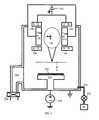
- FIG. 1shows one embodiment of an apparatus for fabricating semiconductor.
- An embodiment reactor 10is schematically illustrated in FIG. 1 .
- the reactor 10includes a metal chamber 14 that is electrically grounded.
- a wafer or substrate 22 to be sputter coatedis supported on a pedestal electrode 24 in opposition to the target 16 .
- An electrical bias source 26is connected to the pedestal electrode 24 .
- the bias source 26is an RF bias source coupled to the pedestal electrode 24 through an isolation capacitor.
- Such bias sourceproduces a negative DC self-bias VB on the pedestal electrode 24 on the order of tens of volts.
- a working gassuch as argon is supplied from a gas source 28 through a mass flow controller 30 and thence through a gas inlet 32 into the chamber.
- a vacuum pump system 34pumps the chamber through a pumping port 36 .
- An FTS unitis positioned to face the wafer 22 and has a plurality of magnets 102 , 104 , 106 , and 108 .
- a first target 110is positioned between magnets 102 and 104
- a second target 120is positioned between magnets 106 and 108 .
- the first and second targets 110 and 120define an electron confining region 130 .
- a power supply 140is connected to the magnets 102 - 108 and targets 110 - 120 so that positive charges are attracted to the second target 120 .
- particlesare sputtered onto a substrate 150 which, in one embodiment where the targets 110 and 120 are laterally positioned, is vertically positioned relative to the lateral targets 110 and 120 .
- the substrate 150is arranged to be perpendicular to the planes of the targets 110 and 120 .
- a substrate holder 152supports the substrate 150 .
- the targets 110 and 120are positioned in the reactor 10 in such a manner that two rectangular shape cathode targets face each other so as to define the plasma confining region 130 therebetween. Magnetic fields are then generated to cover vertically the outside of the space between facing target planes by the arrangement of magnets installed in touch with the backside planes of facing targets 110 and 120 .
- the facing targets 110 and 120are used a cathode, and the shield plates are used as an anode, and the cathode/anode are connected to output terminals of the direct current (DC) power supply 140 .
- the vacuum vessel and the shield platesare also connected to the anode.
- sputtering plasmais formed in the space 130 between the facing targets 110 and 120 while power from the power source is applied. Since magnetic fields are generated around the peripheral area extending in a direction perpendicular to the surfaces of facing targets 110 and 120 , highly energized electrons sputtered from surfaces of the facing targets 110 and 120 are confined in the space between facing targets 110 and 120 to cause increased ionized gases by collision in the space 130 .
- the ionization rate of the sputtering gasescorresponds to the deposition rate of thin films on the substrate 22 , then, high rate deposition is realized due to the confinement of electrons in the space 130 between the facing targets.
- the substrate 22is arranged so as to be isolated from the plasma space between the facing targets 110 and 120 .
- Film deposition on the substrate 22is processed at a low temperature range due to a very small number of impingement of plasma from the plasma space and small amount of thermal radiation from the target planes.
- a typical facing target type of sputtering methodhas superior properties of depositing ferromagnetic materials at high rate deposition and low substrate temperature in comparison with a magnetron sputtering method.
- plasmais excited from the argon.
- the chamber enclosureis grounded.
- the RF power supply 26 to the chuck or pedestal 24causes an effective DC ‘back-bias’ between the wafer and the chamber. This bias is negative, so it repels the low-velocity electrons.
- FIG. 2illustrates an exemplary electron distribution for the apparatus of FIG. 1 .
- the electron distributionfollows a standard Maxwellian curve.
- Low energy electronshave two characteristics: they are numerous and they tend to have non-elastic collisions with the deposited atoms, resulting in amorphization during deposition.
- High-energy electronscome through the back-biased shield, but they effectively “bounce” off the atoms without significant energy transfer—these electrons do not affect the way bonds are formed. This is especially true because high energy electrons spend very little time in the vicinity of the atoms, while the low energy electrons spend more time next to the atoms and can interfere with bond formation.
- the presence of the large positively biased shieldaffects the plasma, particularly close to the pedestal electrode 24 .
- the DC self-bias developed on the pedestal 24may be more positive than for the conventional large grounded shield, that is, less negative since the DC self-bias is negative in typical applications. It is believed that the change in DC self-bias arises from the fact that the positively biased shield drains electrons from the plasma, thereby causing the plasma and hence the pedestal electrode to become more positive.
- FIG. 3shows another embodiment of an FTS system.
- a wafer 200is positioned in a chamber 210 .
- the wafer 200is moved into the chamber 210 using a robot arm 220 .
- the robot arm 220places the wafer 200 on a wafer chuck 230 .
- the wafer chuck 230is moved by a chuck motor 240 .
- One or more chuck heaters 250heats the wafer 200 during processing.
- the wafer 200is positioned between the heater 250 and a magnetron 260 .
- the magnetron 260serves as highly efficient sources of microwave energy.
- microwave magnetronsemploy a constant magnetic field to produce a rotating electron space charge. The space charge interacts with a plurality of microwave resonant cavities to generate microwave radiation.
- One electrical node 270is provided to a back-bias generator such as the generator 26 of FIG. 1 .
- two target platesare respectively connected and disposed onto two target holders which are fixed to both inner ends of the chamber 210 so as to make the target plates face each other.
- a pair of permanent magnetsare accommodated in the target holders so as to create a magnetic field therebetween substantially perpendicular to the surface of the target plates.
- the wafer 200is disposed closely to the magnetic field (which will define a plasma region) so as to preferably face it.
- the electrons emitted from the both target plates by applying the voltageare confined between the target plates because of the magnetic field to promote the ionization of the inert gas so as to form a plasma region.
- the positive ions of the inert gas existing in the plasma regionare accelerated toward the target plates.
- the bombardment of the target plates by the accelerated particles of the inert gas and ions thereofcauses atoms of the material forming the plates to be emitted.
- the wafer 200 on which the thin film is to be disposedis placed around the plasma region, so that the bombardment of these high energy particles and ions against the thin film plane is avoided because of effective confinement of the plasma region by the magnetic field.
- the back-bias RF power supplycauses an effective DC ‘back-bias’ between the wafer 200 and the chamber 210 . This bias is negative, so it repels the low-velocity electrons.
- FIG. 4Ashows one embodiment of an apparatus for fabricating semiconductor.
- multiple 1-D deposition sourcesare stacked in the deposition chamber.
- the stacking of the sourcesreduces the amount of wafer travel, while significantly increasing deposition uniformity.
- a wafer 300is inserted into a chamber 410 using a robot arm 420 moving through a transfer chamber 430 .
- the wafer 300is positioned onto a rotary chuck 440 with chuck heater(s) 450 positioned above the wafer.
- a linear motor 460moves the chuck through a plurality of deposition chambers 470 .
- the system of FIG. 4Aprovides a plurality of one dimensional sputter deposition chambers. Each chamber can deposit a line of material. By moving the wafer 300 with the linear motor 460 , 2-d coverage is obtained.
- a process for obtain 2D deposition coverageis as follows:
- a chuck 500is positioned inside a chamber.
- the chuck 500supports a wafer 502 .
- the chamberhas vacuum bellows 510 .
- the chuck 500is driven by a wafer rotator 520 which rotates the wafer 502 .
- the chuck 500 and the wafer 502has a pendulum motion.
- the chuck 500is also powered by a linear motor 530 to provide up/down motion.
- a plurality of sources 540 - 544perform deposition of materials on the wafer 502 .
- the system of FIG. 4Bgets linear motion of the wafer 502 past the three sources for uniform deposition.
- the systemhas a jointed pendulum to support the wafer and keep the wafer at a constant vertical distance from the target as the pendulum swings.
- the systemis more stable than a system with a lateral linear arm since the chuck 500 is heavy and supports the weight of the wafer, a heater, and RF backbias circuitry and would require a very thick support arm otherwise the arm would wobble.
- the linear armwould need to extend away from the source, resulting in large equipment. In this implementation, the arm sits below the chuck, resulting in a smaller piece of equipment and also the arm does not have to support much weight.
- the pendulumavoids the use of a long linear arm which wobbles and adds at least 4 feet of equipment size. The pendulum holds the wafer much more securely because the chuck is supported from underneath rather than from the side.
- FIG. 5shows an SEM image of an exemplary device fabricated with the system of FIG. 1
- FIG. 6is an enlarged view of one portion of the SEM image of FIG. 5
- the device of FIG. 5was fabricated at a low temperature (below 400° C.).
- an oxide layer(20 nm thick).
- a metal layerin this case a titanium layer (24 nm thick).
- an interface layerin this case a platinum (Pt) interface face layer (about 5 nm).
- Ptplatinum
- a crystallite PCMO layer(79 nm thick) is formed at the top. Grains in this layer can be seen extending from the bottom toward the top with a slightly angled tilt.
- FIG. 6shows a zoomed view showing the Ti metal layer, the Pt interface layer and the PCMO grain in more details.
- FIGS. 7A-7Cillustrate an exemplary deposition sequence for the above described equipment.
- the processdeposits a layer of material on the substrate and exposes a resist film to an electron beam and then develop the resist film to form a pattern on the resist film.
- a mask materialis deposited, and the resist film is dissolved to form a mask.
- the substrateis back-biased and a part of the film which is not covered by said mask is removed by face target sputtering with a metal to form a pattern on the layer.
- a copper layer 700is deposited. Above the copper layer 700 , a titanium layer 702 is deposited. Both layers are lithographically patterned to create lines which will be used to connect the memory cells. Next, a silicon nitride layer 704 is formed and patterned with holes to allow electrical contact to the platinum layer underneath. Next a platinum layer 708 is formed above the titanium layer 702 . A platinum layer 706 is then formed above the silicon dioxide layer 704 . The platinum layer 706 is deposited anisotropically, resulting in a disconnect between the platinum over the silicon nitride and the platinum over the titanium exposed by the silicon nitride holes.
- the platinum layer 706is removed by bombardment from positive ions.
- the ionsare accelerated near the surface by a dual voltage imposed on the metallized surface.
- the portions of the platinum laying on the insulating silicon nitrideare negatively charged by the large negative AC voltage 720 , causing an enhanced etch rate.
- This voltageis AC coupled to the platinum layer through the silicon nitride layer.
- the platinum connected to the titanium 702is connected to an only slightly negative DC voltage 721 , resulting in virtually no etching.
- CMO layers 706 , 710 and 712are formed above the wafer of FIG. 7A .
- CMOdoes not form on the silicon nitride because the high negative voltage causes any deposited ions to be re-sputtered by new positive ions.
- platinum layers 714 - 716are deposited above the CMO layers 706 and 710 , respectively. Again, the platinum is only deposited on top of the CMO because of the favorable bias.
- This biasing etch-deposition processcan be used to deposit the entire platinum-CMO memory stack in the deposition chamber without breaking vacuum, and without the need of an intermediate lithography step to define the stack.
- a dielectric layeris deposited and planarized with chemical-mechanical polishing. The part is then completed using a standard copper damascene process.
- FIG. 8shows an exemplary cross-section view of a device fabricated in accordance with the above described system.
- a low constant dielectric layer 802is formed above the substrate.
- a tantalum electromigration barrier 804isolates a metal line 806 from the dielectric layer 802 .
- Above the dielectric layer 802is a nitride isolation layer 810 .
- Another low constant dielectric layer 824is positioned above the second nitride isolation layer 810 .
- the layer 810is 300 Angstroms thick.
- a cross copper metal line 828is formed above the entire section. In one embodiment, the metal line 828 is 1000 Angstroms thick.
- a titanium or titanium nitride layer 812Above the metal line 806 is a titanium or titanium nitride layer 812 .
- a platinum layer 814is then formed.
- a CMO layer 816is then sandwiched between the platinum layer 814 and a second platinum layer 818 .
- Another titanium or titanium nitride layer 820is formed above the platinum layer 818 .
- a copper damascene via 826is formed between the copper metal line 828 and the titanium or titanium nitride layer 820 .
- the damascene viais 1000 Angstroms thick.
- back-biased power suppliesAlthough one or two back-biased power supplies are mentioned, a plurality of back-bias power supplies can be used. These power supplies can be controllable independently from each other, and their operating frequency can be varied. The electric energies supplied can be independently controlled. Therefore, the components of the thin film to be formed are easily controlled in every sputtering batch process. In addition, the composition of the thin film can be changed in the direction of the thickness of the film by using the Facing Targets Sputtering device.
- the inventionhas been described in terms of specific examples which are illustrative only and are not to be construed as limiting.
- the inventionmay be implemented in digital electronic circuitry or in computer hardware, firmware, software, or in combinations of them.
- Apparatus of the invention for controlling the fabrication equipmentmay be implemented in a computer program product tangibly embodied in a machine-readable storage device for execution by a computer processor; and method steps of the invention may be performed by a computer processor executing a program to perform functions of the invention by operating on input data and generating output.
- Suitable processorsinclude, by way of example, both general and special purpose microprocessors.
- Storage devices suitable for tangibly embodying computer program instructionsinclude all forms of non-volatile memory including, but not limited to: semiconductor memory devices such as EPROM, EEPROM, and flash devices; magnetic disks (fixed, floppy, and removable); other magnetic media such as tape; optical media such as CD-ROM disks; and magneto-optic devices. Any of the foregoing may be supplemented by, or incorporated in, specially-designed application-specific integrated circuits (ASICs) or suitably programmed field programmable gate arrays (FPGAs).
- ASICsapplication-specific integrated circuits
- FPGAsfield programm
Landscapes
- Engineering & Computer Science (AREA)
- Chemical & Material Sciences (AREA)
- Power Engineering (AREA)
- Organic Chemistry (AREA)
- Mechanical Engineering (AREA)
- Metallurgy (AREA)
- Materials Engineering (AREA)
- Physics & Mathematics (AREA)
- Condensed Matter Physics & Semiconductors (AREA)
- General Physics & Mathematics (AREA)
- Manufacturing & Machinery (AREA)
- Computer Hardware Design (AREA)
- Microelectronics & Electronic Packaging (AREA)
- Chemical Kinetics & Catalysis (AREA)
- Physical Vapour Deposition (AREA)
Abstract
Description
- Receive desired 2D pattern from user
- Move chuck into a selected deposition chamber;
- Actuate linear motor and rotary chuck to in accordance with the 2D pattern
- Move current wafer to next deposition chamber
- Get next wafer into the current chamber and repeat process.
Claims (20)
Priority Applications (1)
| Application Number | Priority Date | Filing Date | Title |
|---|---|---|---|
| US10/966,384US7425504B2 (en) | 2004-10-15 | 2004-10-15 | Systems and methods for plasma etching |
Applications Claiming Priority (1)
| Application Number | Priority Date | Filing Date | Title |
|---|---|---|---|
| US10/966,384US7425504B2 (en) | 2004-10-15 | 2004-10-15 | Systems and methods for plasma etching |
Publications (2)
| Publication Number | Publication Date |
|---|---|
| US20060276036A1 US20060276036A1 (en) | 2006-12-07 |
| US7425504B2true US7425504B2 (en) | 2008-09-16 |
Family
ID=37494713
Family Applications (1)
| Application Number | Title | Priority Date | Filing Date |
|---|---|---|---|
| US10/966,384Expired - LifetimeUS7425504B2 (en) | 2004-10-15 | 2004-10-15 | Systems and methods for plasma etching |
Country Status (1)
| Country | Link |
|---|---|
| US (1) | US7425504B2 (en) |
Families Citing this family (3)
| Publication number | Priority date | Publication date | Assignee | Title |
|---|---|---|---|---|
| US8395199B2 (en)* | 2006-03-25 | 2013-03-12 | 4D-S Pty Ltd. | Systems and methods for fabricating self-aligned memory cell |
| US20130101372A1 (en)* | 2011-10-19 | 2013-04-25 | Lam Research Ag | Method and apparatus for processing wafer-shaped articles |
| JP2015070232A (en)* | 2013-09-30 | 2015-04-13 | 株式会社東芝 | Semiconductor device manufacturing method and semiconductor manufacturing device |
Citations (1)
| Publication number | Priority date | Publication date | Assignee | Title |
|---|---|---|---|---|
| US6962648B2 (en)* | 2003-09-15 | 2005-11-08 | Global Silicon Net Corp. | Back-biased face target sputtering |
Family Cites Families (74)
| Publication number | Priority date | Publication date | Assignee | Title |
|---|---|---|---|---|
| US4664935A (en)* | 1985-09-24 | 1987-05-12 | Machine Technology, Inc. | Thin film deposition apparatus and method |
| JPH02217467A (en)* | 1989-02-17 | 1990-08-30 | Pioneer Electron Corp | Opposite target type sputtering device |
| DE3920835C2 (en)* | 1989-06-24 | 1997-12-18 | Leybold Ag | Device for coating substrates |
| US5286296A (en)* | 1991-01-10 | 1994-02-15 | Sony Corporation | Multi-chamber wafer process equipment having plural, physically communicating transfer means |
| US5415754A (en)* | 1993-10-22 | 1995-05-16 | Sierra Applied Sciences, Inc. | Method and apparatus for sputtering magnetic target materials |
| DE69833046T2 (en)* | 1997-03-11 | 2006-08-03 | Agfa-Gevaert | Process for the preparation of a lithographic printing plate |
| JPH11302839A (en)* | 1998-04-17 | 1999-11-02 | Toshiba Corp | Sputtering equipment |
| US6204139B1 (en)* | 1998-08-25 | 2001-03-20 | University Of Houston | Method for switching the properties of perovskite materials used in thin film resistors |
| US6899795B1 (en)* | 2000-01-18 | 2005-05-31 | Unaxis Balzers Aktiengesellschaft | Sputter chamber as well as vacuum transport chamber and vacuum handling apparatus with such chambers |
| US6342133B2 (en)* | 2000-03-14 | 2002-01-29 | Novellus Systems, Inc. | PVD deposition of titanium and titanium nitride layers in the same chamber without use of a collimator or a shutter |
| SG90171A1 (en)* | 2000-09-26 | 2002-07-23 | Inst Data Storage | Sputtering device |
| US6524867B2 (en)* | 2000-12-28 | 2003-02-25 | Micron Technology, Inc. | Method for forming platinum-rhodium stack as an oxygen barrier |
| US6569745B2 (en)* | 2001-06-28 | 2003-05-27 | Sharp Laboratories Of America, Inc. | Shared bit line cross point memory array |
| US6825058B2 (en)* | 2001-06-28 | 2004-11-30 | Sharp Laboratories Of America, Inc. | Methods of fabricating trench isolated cross-point memory array |
| US6905937B2 (en)* | 2001-06-28 | 2005-06-14 | Sharp Laboratories Of America, Inc. | Methods of fabricating a cross-point resistor memory array |
| US6693821B2 (en)* | 2001-06-28 | 2004-02-17 | Sharp Laboratories Of America, Inc. | Low cross-talk electrically programmable resistance cross point memory |
| US6531371B2 (en)* | 2001-06-28 | 2003-03-11 | Sharp Laboratories Of America, Inc. | Electrically programmable resistance cross point memory |
| US7193267B2 (en)* | 2001-06-28 | 2007-03-20 | Sharp Laboratories Of America, Inc. | Cross-point resistor memory array |
| US6759249B2 (en)* | 2002-02-07 | 2004-07-06 | Sharp Laboratories Of America, Inc. | Device and method for reversible resistance change induced by electric pulses in non-crystalline perovskite unipolar programmable memory |
| US6654210B2 (en)* | 2002-04-22 | 2003-11-25 | Sharp Laboratories Of America, Inc. | Solid-state inductor and method for same |
| JP4282314B2 (en)* | 2002-06-25 | 2009-06-17 | シャープ株式会社 | Storage device |
| US6753561B1 (en)* | 2002-08-02 | 2004-06-22 | Unity Semiconductor Corporation | Cross point memory array using multiple thin films |
| US7038935B2 (en)* | 2002-08-02 | 2006-05-02 | Unity Semiconductor Corporation | 2-terminal trapped charge memory device with voltage switchable multi-level resistance |
| US7042035B2 (en)* | 2002-08-02 | 2006-05-09 | Unity Semiconductor Corporation | Memory array with high temperature wiring |
| US7009235B2 (en)* | 2003-11-10 | 2006-03-07 | Unity Semiconductor Corporation | Conductive memory stack with non-uniform width |
| US6870755B2 (en)* | 2002-08-02 | 2005-03-22 | Unity Semiconductor Corporation | Re-writable memory with non-linear memory element |
| US6831854B2 (en)* | 2002-08-02 | 2004-12-14 | Unity Semiconductor Corporation | Cross point memory array using distinct voltages |
| US7020006B2 (en)* | 2002-08-02 | 2006-03-28 | Unity Semiconductor Corporation | Discharge of conductive array lines in fast memory |
| US6970375B2 (en)* | 2002-08-02 | 2005-11-29 | Unity Semiconductor Corporation | Providing a reference voltage to a cross point memory array |
| US6850429B2 (en)* | 2002-08-02 | 2005-02-01 | Unity Semiconductor Corporation | Cross point memory array with memory plugs exhibiting a characteristic hysteresis |
| US6917539B2 (en)* | 2002-08-02 | 2005-07-12 | Unity Semiconductor Corporation | High-density NVRAM |
| US7009909B2 (en)* | 2002-08-02 | 2006-03-07 | Unity Semiconductor Corporation | Line drivers that use minimal metal layers |
| US6850455B2 (en)* | 2002-08-02 | 2005-02-01 | Unity Semiconductor Corporation | Multiplexor having a reference voltage on unselected lines |
| US6859382B2 (en)* | 2002-08-02 | 2005-02-22 | Unity Semiconductor Corporation | Memory array of a non-volatile ram |
| US6583003B1 (en)* | 2002-09-26 | 2003-06-24 | Sharp Laboratories Of America, Inc. | Method of fabricating 1T1R resistive memory array |
| US6746910B2 (en)* | 2002-09-30 | 2004-06-08 | Sharp Laboratories Of America, Inc. | Method of fabricating self-aligned cross-point memory array |
| US6940744B2 (en)* | 2002-10-31 | 2005-09-06 | Unity Semiconductor Corporation | Adaptive programming technique for a re-writable conductive memory device |
| JP2004158119A (en)* | 2002-11-06 | 2004-06-03 | Sharp Corp | Nonvolatile semiconductor memory device |
| US6851687B2 (en)* | 2002-11-26 | 2005-02-08 | Daimlerchrysler Corporation | Off-axis cam adjustment system and method |
| US6801448B2 (en)* | 2002-11-26 | 2004-10-05 | Sharp Laboratories Of America, Inc. | Common bit/common source line high density 1T1R R-RAM array |
| JP2004185755A (en)* | 2002-12-05 | 2004-07-02 | Sharp Corp | Nonvolatile semiconductor memory device |
| US6887523B2 (en)* | 2002-12-20 | 2005-05-03 | Sharp Laboratories Of America, Inc. | Method for metal oxide thin film deposition via MOCVD |
| US6875651B2 (en)* | 2003-01-23 | 2005-04-05 | Sharp Laboratories Of America, Inc. | Dual-trench isolated crosspoint memory array and method for fabricating same |
| US6849564B2 (en)* | 2003-02-27 | 2005-02-01 | Sharp Laboratories Of America, Inc. | 1R1D R-RAM array with floating p-well |
| JP2004273656A (en)* | 2003-03-07 | 2004-09-30 | Taiyo Yuden Co Ltd | EPIR element and semiconductor device using the same |
| US6868025B2 (en)* | 2003-03-10 | 2005-03-15 | Sharp Laboratories Of America, Inc. | Temperature compensated RRAM circuit |
| US6723643B1 (en)* | 2003-03-17 | 2004-04-20 | Sharp Laboratories Of America, Inc. | Method for chemical mechanical polishing of thin films using end-point indicator structures |
| US6774004B1 (en)* | 2003-03-17 | 2004-08-10 | Sharp Laboratories Of America, Inc. | Nano-scale resistance cross-point memory array |
| US7001846B2 (en)* | 2003-05-20 | 2006-02-21 | Sharp Laboratories Of America, Inc. | High-density SOI cross-point memory array and method for fabricating same |
| US6972238B2 (en)* | 2003-05-21 | 2005-12-06 | Sharp Laboratories Of America, Inc. | Oxygen content system and method for controlling memory resistance properties |
| JP4113493B2 (en)* | 2003-06-12 | 2008-07-09 | シャープ株式会社 | Nonvolatile semiconductor memory device and control method thereof |
| JP2005032401A (en)* | 2003-06-17 | 2005-02-03 | Sharp Corp | Nonvolatile semiconductor memory device and writing method and erasing method thereof |
| US6939724B2 (en)* | 2003-08-13 | 2005-09-06 | Sharp Laboratories Of America, Inc. | Method for obtaining reversible resistance switches on a PCMO thin film when integrated with a highly crystallized seed layer |
| US7029924B2 (en)* | 2003-09-05 | 2006-04-18 | Sharp Laboratories Of America, Inc. | Buffered-layer memory cell |
| JP4192060B2 (en)* | 2003-09-12 | 2008-12-03 | シャープ株式会社 | Nonvolatile semiconductor memory device |
| US6955992B2 (en)* | 2003-09-30 | 2005-10-18 | Sharp Laboratories Of America, Inc. | One mask PT/PCMO/PT stack etching process for RRAM applications |
| JP2005167064A (en)* | 2003-12-04 | 2005-06-23 | Sharp Corp | Nonvolatile semiconductor memory device |
| US6949435B2 (en)* | 2003-12-08 | 2005-09-27 | Sharp Laboratories Of America, Inc. | Asymmetric-area memory cell |
| US6849891B1 (en)* | 2003-12-08 | 2005-02-01 | Sharp Laboratories Of America, Inc. | RRAM memory cell electrodes |
| US7095644B2 (en)* | 2003-12-22 | 2006-08-22 | Unity Semiconductor Corporation | Conductive memory array having page mode and burst mode read capability |
| US7099179B2 (en)* | 2003-12-22 | 2006-08-29 | Unity Semiconductor Corporation | Conductive memory array having page mode and burst mode write capability |
| US7016094B2 (en)* | 2004-01-12 | 2006-03-21 | Sharp Laboratories Of America, Inc. | Nonvolatile solid state electro-optic modulator |
| JP4153901B2 (en)* | 2004-06-15 | 2008-09-24 | シャープ株式会社 | Semiconductor memory device |
| JP4365737B2 (en)* | 2004-06-30 | 2009-11-18 | シャープ株式会社 | Method of driving variable resistance element and storage device |
| US7169637B2 (en)* | 2004-07-01 | 2007-01-30 | Sharp Laboratories Of America, Inc. | One mask Pt/PCMO/Pt stack etching process for RRAM applications |
| US7330370B2 (en)* | 2004-07-20 | 2008-02-12 | Unity Semiconductor Corporation | Enhanced functionality in a two-terminal memory array |
| US7075817B2 (en)* | 2004-07-20 | 2006-07-11 | Unity Semiconductor Corporation | Two terminal memory array having reference cells |
| US7084691B2 (en)* | 2004-07-21 | 2006-08-01 | Sharp Laboratories Of America, Inc. | Mono-polarity switchable PCMO resistor trimmer |
| JP4189395B2 (en)* | 2004-07-28 | 2008-12-03 | シャープ株式会社 | Nonvolatile semiconductor memory device and reading method |
| US20060068099A1 (en)* | 2004-09-30 | 2006-03-30 | Sharp Laboratories Of America, Inc. | Grading PrxCa1-xMnO3 thin films by metalorganic chemical vapor deposition |
| US7339813B2 (en)* | 2004-09-30 | 2008-03-04 | Sharp Laboratories Of America, Inc. | Complementary output resistive memory cell |
| US7205238B2 (en)* | 2004-10-21 | 2007-04-17 | Sharp Laboratories Of America, Inc. | Chemical mechanical polish of PCMO thin films for RRAM applications |
| US7029982B1 (en)* | 2004-10-21 | 2006-04-18 | Sharp Laboratories Of America, Inc. | Method of affecting RRAM characteristics by doping PCMO thin films |
| JP4880894B2 (en)* | 2004-11-17 | 2012-02-22 | シャープ株式会社 | Semiconductor memory device structure and manufacturing method thereof |
- 2004
- 2004-10-15USUS10/966,384patent/US7425504B2/ennot_activeExpired - Lifetime
Patent Citations (1)
| Publication number | Priority date | Publication date | Assignee | Title |
|---|---|---|---|---|
| US6962648B2 (en)* | 2003-09-15 | 2005-11-08 | Global Silicon Net Corp. | Back-biased face target sputtering |
Also Published As
| Publication number | Publication date |
|---|---|
| US20060276036A1 (en) | 2006-12-07 |
Similar Documents
| Publication | Publication Date | Title |
|---|---|---|
| KR101182072B1 (en) | Apparatus for low temperature semiconductor fabrication | |
| US7230258B2 (en) | Plasma-based debris mitigation for extreme ultraviolet (EUV) light source | |
| US6960284B2 (en) | Rotational and reciprocal radial movement of a sputtering magnetron | |
| US5627105A (en) | Plasma etch process and TiSix layers made using the process | |
| JP4344019B2 (en) | Ionized sputtering method | |
| US8911602B2 (en) | Dual hexagonal shaped plasma source | |
| CN1957104A (en) | Method and apparatus for plasma treatment | |
| US20070007124A1 (en) | Back-biased face target sputtering based memory with low oxygen flow rate | |
| KR20010099597A (en) | Physical vapor processing of a surface with non-uniformity compensation | |
| WO2011002058A1 (en) | Method for depositing thin film | |
| JP4614578B2 (en) | Plasma processing equipment for sputter deposition applications | |
| JP4326895B2 (en) | Sputtering equipment | |
| US8016985B2 (en) | Magnetron sputtering apparatus and method for manufacturing semiconductor device | |
| US7425504B2 (en) | Systems and methods for plasma etching | |
| JP4408987B2 (en) | Plasma processing equipment for sputter processing | |
| US20060081466A1 (en) | High uniformity 1-D multiple magnet magnetron source | |
| US20060081467A1 (en) | Systems and methods for magnetron deposition | |
| TW202518519A (en) | Apparatus and method for enhanced plasma control | |
| US20060231384A1 (en) | Back-biased face target sputtering | |
| JP2004269939A (en) | Sputtering apparatus, sputtering method and semiconductor device | |
| JP5069255B2 (en) | Sputtering apparatus and sputtering method | |
| US20240105425A1 (en) | Substrate processing apparatus and method of processing substrate by using the same | |
| JP2011208185A (en) | Sputtering apparatus | |
| WO2024085938A1 (en) | Resonant antenna for physical vapor deposition applications | |
| JP2009052145A (en) | Sputtering equipment |
Legal Events
| Date | Code | Title | Description |
|---|---|---|---|
| AS | Assignment | Owner name:4D-S PTY LTD., AUSTRALIA Free format text:CORRECTIVE ASSIGNMENT TO CORRECT THE FOLLOWING SERIAL NUMBERS;ASSIGNORS:NAGASHIMA, MAKOTO MARK;GLOBAL SILICON NET, LTD.;REEL/FRAME:021036/0854 Effective date:20080416 | |
| STCF | Information on status: patent grant | Free format text:PATENTED CASE | |
| FPAY | Fee payment | Year of fee payment:4 | |
| AS | Assignment | Owner name:4D-S PTY, LTD, AUSTRALIA Free format text:ASSIGNMENT OF ASSIGNORS INTEREST;ASSIGNOR:SCHMIDT, DOMINIK;REEL/FRAME:036491/0510 Effective date:20150817 | |
| FPAY | Fee payment | Year of fee payment:8 | |
| FEPP | Fee payment procedure | Free format text:MAINTENANCE FEE REMINDER MAILED (ORIGINAL EVENT CODE: REM.); ENTITY STATUS OF PATENT OWNER: SMALL ENTITY | |
| LAPS | Lapse for failure to pay maintenance fees | Free format text:PATENT EXPIRED FOR FAILURE TO PAY MAINTENANCE FEES (ORIGINAL EVENT CODE: EXP.); ENTITY STATUS OF PATENT OWNER: SMALL ENTITY | |
| STCH | Information on status: patent discontinuation | Free format text:PATENT EXPIRED DUE TO NONPAYMENT OF MAINTENANCE FEES UNDER 37 CFR 1.362 | |
| FP | Lapsed due to failure to pay maintenance fee | Effective date:20200916 | |
| FEPP | Fee payment procedure | Free format text:PETITION RELATED TO MAINTENANCE FEES FILED (ORIGINAL EVENT CODE: PMFP); ENTITY STATUS OF PATENT OWNER: SMALL ENTITY Free format text:SURCHARGE, PETITION TO ACCEPT PYMT AFTER EXP, UNINTENTIONAL. (ORIGINAL EVENT CODE: M2558); ENTITY STATUS OF PATENT OWNER: SMALL ENTITY | |
| MAFP | Maintenance fee payment | Free format text:PAYMENT OF MAINTENANCE FEE, 12TH YR, SMALL ENTITY (ORIGINAL EVENT CODE: M2553); ENTITY STATUS OF PATENT OWNER: SMALL ENTITY Year of fee payment:12 | |
| PRDP | Patent reinstated due to the acceptance of a late maintenance fee | Effective date:20220120 | |
| FEPP | Fee payment procedure | Free format text:PETITION RELATED TO MAINTENANCE FEES GRANTED (ORIGINAL EVENT CODE: PMFG); ENTITY STATUS OF PATENT OWNER: SMALL ENTITY | |
| STCF | Information on status: patent grant | Free format text:PATENTED CASE |