US7425462B2 - Methods relating to the reconstruction of semiconductor wafers for wafer-level processing - Google Patents
Methods relating to the reconstruction of semiconductor wafers for wafer-level processingDownload PDFInfo
- Publication number
- US7425462B2 US7425462B2US11/449,472US44947206AUS7425462B2US 7425462 B2US7425462 B2US 7425462B2US 44947206 AUS44947206 AUS 44947206AUS 7425462 B2US7425462 B2US 7425462B2
- Authority
- US
- United States
- Prior art keywords
- alignment
- semiconductor die
- droplet
- wafer
- process according
- Prior art date
- Legal status (The legal status is an assumption and is not a legal conclusion. Google has not performed a legal analysis and makes no representation as to the accuracy of the status listed.)
- Expired - Lifetime, expires
Links
Images


Classifications
- H—ELECTRICITY
- H01—ELECTRIC ELEMENTS
- H01L—SEMICONDUCTOR DEVICES NOT COVERED BY CLASS H10
- H01L24/00—Arrangements for connecting or disconnecting semiconductor or solid-state bodies; Methods or apparatus related thereto
- H01L24/93—Batch processes
- H01L24/95—Batch processes at chip-level, i.e. with connecting carried out on a plurality of singulated devices, i.e. on diced chips
- H01L24/96—Batch processes at chip-level, i.e. with connecting carried out on a plurality of singulated devices, i.e. on diced chips the devices being encapsulated in a common layer, e.g. neo-wafer or pseudo-wafer, said common layer being separable into individual assemblies after connecting
- H—ELECTRICITY
- H01—ELECTRIC ELEMENTS
- H01L—SEMICONDUCTOR DEVICES NOT COVERED BY CLASS H10
- H01L21/00—Processes or apparatus adapted for the manufacture or treatment of semiconductor or solid state devices or of parts thereof
- H01L21/67—Apparatus specially adapted for handling semiconductor or electric solid state devices during manufacture or treatment thereof; Apparatus specially adapted for handling wafers during manufacture or treatment of semiconductor or electric solid state devices or components ; Apparatus not specifically provided for elsewhere
- H01L21/683—Apparatus specially adapted for handling semiconductor or electric solid state devices during manufacture or treatment thereof; Apparatus specially adapted for handling wafers during manufacture or treatment of semiconductor or electric solid state devices or components ; Apparatus not specifically provided for elsewhere for supporting or gripping
- H01L21/6835—Apparatus specially adapted for handling semiconductor or electric solid state devices during manufacture or treatment thereof; Apparatus specially adapted for handling wafers during manufacture or treatment of semiconductor or electric solid state devices or components ; Apparatus not specifically provided for elsewhere for supporting or gripping using temporarily an auxiliary support
- H—ELECTRICITY
- H01—ELECTRIC ELEMENTS
- H01L—SEMICONDUCTOR DEVICES NOT COVERED BY CLASS H10
- H01L23/00—Details of semiconductor or other solid state devices
- H01L23/48—Arrangements for conducting electric current to or from the solid state body in operation, e.g. leads, terminal arrangements ; Selection of materials therefor
- H01L23/481—Internal lead connections, e.g. via connections, feedthrough structures
- H—ELECTRICITY
- H01—ELECTRIC ELEMENTS
- H01L—SEMICONDUCTOR DEVICES NOT COVERED BY CLASS H10
- H01L25/00—Assemblies consisting of a plurality of semiconductor or other solid state devices
- H01L25/03—Assemblies consisting of a plurality of semiconductor or other solid state devices all the devices being of a type provided for in a single subclass of subclasses H10B, H10D, H10F, H10H, H10K or H10N, e.g. assemblies of rectifier diodes
- H01L25/04—Assemblies consisting of a plurality of semiconductor or other solid state devices all the devices being of a type provided for in a single subclass of subclasses H10B, H10D, H10F, H10H, H10K or H10N, e.g. assemblies of rectifier diodes the devices not having separate containers
- H01L25/065—Assemblies consisting of a plurality of semiconductor or other solid state devices all the devices being of a type provided for in a single subclass of subclasses H10B, H10D, H10F, H10H, H10K or H10N, e.g. assemblies of rectifier diodes the devices not having separate containers the devices being of a type provided for in group H10D89/00
- H01L25/0655—Assemblies consisting of a plurality of semiconductor or other solid state devices all the devices being of a type provided for in a single subclass of subclasses H10B, H10D, H10F, H10H, H10K or H10N, e.g. assemblies of rectifier diodes the devices not having separate containers the devices being of a type provided for in group H10D89/00 the devices being arranged next to each other
- H—ELECTRICITY
- H01—ELECTRIC ELEMENTS
- H01L—SEMICONDUCTOR DEVICES NOT COVERED BY CLASS H10
- H01L25/00—Assemblies consisting of a plurality of semiconductor or other solid state devices
- H01L25/50—Multistep manufacturing processes of assemblies consisting of devices, the devices being individual devices of subclass H10D or integrated devices of class H10
- H—ELECTRICITY
- H10—SEMICONDUCTOR DEVICES; ELECTRIC SOLID-STATE DEVICES NOT OTHERWISE PROVIDED FOR
- H10D—INORGANIC ELECTRIC SEMICONDUCTOR DEVICES
- H10D62/00—Semiconductor bodies, or regions thereof, of devices having potential barriers
- H10D62/10—Shapes, relative sizes or dispositions of the regions of the semiconductor bodies; Shapes of the semiconductor bodies
- H10D62/117—Shapes of semiconductor bodies
- H—ELECTRICITY
- H01—ELECTRIC ELEMENTS
- H01L—SEMICONDUCTOR DEVICES NOT COVERED BY CLASS H10
- H01L2221/00—Processes or apparatus adapted for the manufacture or treatment of semiconductor or solid state devices or of parts thereof covered by H01L21/00
- H01L2221/67—Apparatus for handling semiconductor or electric solid state devices during manufacture or treatment thereof; Apparatus for handling wafers during manufacture or treatment of semiconductor or electric solid state devices or components; Apparatus not specifically provided for elsewhere
- H01L2221/683—Apparatus for handling semiconductor or electric solid state devices during manufacture or treatment thereof; Apparatus for handling wafers during manufacture or treatment of semiconductor or electric solid state devices or components; Apparatus not specifically provided for elsewhere for supporting or gripping
- H01L2221/68304—Apparatus for handling semiconductor or electric solid state devices during manufacture or treatment thereof; Apparatus for handling wafers during manufacture or treatment of semiconductor or electric solid state devices or components; Apparatus not specifically provided for elsewhere for supporting or gripping using temporarily an auxiliary support
- H01L2221/68309—Auxiliary support including alignment aids
- H—ELECTRICITY
- H01—ELECTRIC ELEMENTS
- H01L—SEMICONDUCTOR DEVICES NOT COVERED BY CLASS H10
- H01L2224/00—Indexing scheme for arrangements for connecting or disconnecting semiconductor or solid-state bodies and methods related thereto as covered by H01L24/00
- H01L2224/01—Means for bonding being attached to, or being formed on, the surface to be connected, e.g. chip-to-package, die-attach, "first-level" interconnects; Manufacturing methods related thereto
- H01L2224/02—Bonding areas; Manufacturing methods related thereto
- H01L2224/04—Structure, shape, material or disposition of the bonding areas prior to the connecting process
- H01L2224/05—Structure, shape, material or disposition of the bonding areas prior to the connecting process of an individual bonding area
- H01L2224/0554—External layer
- H01L2224/05573—Single external layer
- H—ELECTRICITY
- H01—ELECTRIC ELEMENTS
- H01L—SEMICONDUCTOR DEVICES NOT COVERED BY CLASS H10
- H01L2224/00—Indexing scheme for arrangements for connecting or disconnecting semiconductor or solid-state bodies and methods related thereto as covered by H01L24/00
- H01L2224/01—Means for bonding being attached to, or being formed on, the surface to be connected, e.g. chip-to-package, die-attach, "first-level" interconnects; Manufacturing methods related thereto
- H01L2224/10—Bump connectors; Manufacturing methods related thereto
- H01L2224/11—Manufacturing methods
- H01L2224/113—Manufacturing methods by local deposition of the material of the bump connector
- H01L2224/1133—Manufacturing methods by local deposition of the material of the bump connector in solid form
- H01L2224/11334—Manufacturing methods by local deposition of the material of the bump connector in solid form using preformed bumps
- H—ELECTRICITY
- H01—ELECTRIC ELEMENTS
- H01L—SEMICONDUCTOR DEVICES NOT COVERED BY CLASS H10
- H01L2224/00—Indexing scheme for arrangements for connecting or disconnecting semiconductor or solid-state bodies and methods related thereto as covered by H01L24/00
- H01L2224/01—Means for bonding being attached to, or being formed on, the surface to be connected, e.g. chip-to-package, die-attach, "first-level" interconnects; Manufacturing methods related thereto
- H01L2224/10—Bump connectors; Manufacturing methods related thereto
- H01L2224/15—Structure, shape, material or disposition of the bump connectors after the connecting process
- H01L2224/16—Structure, shape, material or disposition of the bump connectors after the connecting process of an individual bump connector
- H—ELECTRICITY
- H01—ELECTRIC ELEMENTS
- H01L—SEMICONDUCTOR DEVICES NOT COVERED BY CLASS H10
- H01L2924/00—Indexing scheme for arrangements or methods for connecting or disconnecting semiconductor or solid-state bodies as covered by H01L24/00
- H01L2924/01—Chemical elements
- H01L2924/01005—Boron [B]
- H—ELECTRICITY
- H01—ELECTRIC ELEMENTS
- H01L—SEMICONDUCTOR DEVICES NOT COVERED BY CLASS H10
- H01L2924/00—Indexing scheme for arrangements or methods for connecting or disconnecting semiconductor or solid-state bodies as covered by H01L24/00
- H01L2924/01—Chemical elements
- H01L2924/01006—Carbon [C]
- H—ELECTRICITY
- H01—ELECTRIC ELEMENTS
- H01L—SEMICONDUCTOR DEVICES NOT COVERED BY CLASS H10
- H01L2924/00—Indexing scheme for arrangements or methods for connecting or disconnecting semiconductor or solid-state bodies as covered by H01L24/00
- H01L2924/01—Chemical elements
- H01L2924/01013—Aluminum [Al]
- H—ELECTRICITY
- H01—ELECTRIC ELEMENTS
- H01L—SEMICONDUCTOR DEVICES NOT COVERED BY CLASS H10
- H01L2924/00—Indexing scheme for arrangements or methods for connecting or disconnecting semiconductor or solid-state bodies as covered by H01L24/00
- H01L2924/01—Chemical elements
- H01L2924/01033—Arsenic [As]
- H—ELECTRICITY
- H01—ELECTRIC ELEMENTS
- H01L—SEMICONDUCTOR DEVICES NOT COVERED BY CLASS H10
- H01L2924/00—Indexing scheme for arrangements or methods for connecting or disconnecting semiconductor or solid-state bodies as covered by H01L24/00
- H01L2924/01—Chemical elements
- H01L2924/01047—Silver [Ag]
- H—ELECTRICITY
- H01—ELECTRIC ELEMENTS
- H01L—SEMICONDUCTOR DEVICES NOT COVERED BY CLASS H10
- H01L2924/00—Indexing scheme for arrangements or methods for connecting or disconnecting semiconductor or solid-state bodies as covered by H01L24/00
- H01L2924/01—Chemical elements
- H01L2924/01049—Indium [In]
- H—ELECTRICITY
- H01—ELECTRIC ELEMENTS
- H01L—SEMICONDUCTOR DEVICES NOT COVERED BY CLASS H10
- H01L2924/00—Indexing scheme for arrangements or methods for connecting or disconnecting semiconductor or solid-state bodies as covered by H01L24/00
- H01L2924/01—Chemical elements
- H01L2924/01079—Gold [Au]
- H—ELECTRICITY
- H01—ELECTRIC ELEMENTS
- H01L—SEMICONDUCTOR DEVICES NOT COVERED BY CLASS H10
- H01L2924/00—Indexing scheme for arrangements or methods for connecting or disconnecting semiconductor or solid-state bodies as covered by H01L24/00
- H01L2924/01—Chemical elements
- H01L2924/01082—Lead [Pb]
- H—ELECTRICITY
- H01—ELECTRIC ELEMENTS
- H01L—SEMICONDUCTOR DEVICES NOT COVERED BY CLASS H10
- H01L2924/00—Indexing scheme for arrangements or methods for connecting or disconnecting semiconductor or solid-state bodies as covered by H01L24/00
- H01L2924/10—Details of semiconductor or other solid state devices to be connected
- H01L2924/11—Device type
- H01L2924/12—Passive devices, e.g. 2 terminal devices
- H01L2924/1204—Optical Diode
- H01L2924/12042—LASER
- H—ELECTRICITY
- H01—ELECTRIC ELEMENTS
- H01L—SEMICONDUCTOR DEVICES NOT COVERED BY CLASS H10
- H01L2924/00—Indexing scheme for arrangements or methods for connecting or disconnecting semiconductor or solid-state bodies as covered by H01L24/00
- H01L2924/10—Details of semiconductor or other solid state devices to be connected
- H01L2924/11—Device type
- H01L2924/14—Integrated circuits
Definitions
- the present inventionrelates to the processing of semiconductor wafers and dice. More particularly, but not necessarily limited thereto, it relates to reconstructing semiconductor wafers using only semiconductor dice that are not known to contain defects to retain the benefits of wafer-level processing while reducing resources spent on processing defective dice.
- One such approachis to track the defective dice on each wafer. As the wafer is processed, initial probe testing of the die sites is conducted as is appropriate. Die sites that are known to be defective are tracked by the processing equipment and, where possible, are omitted from subsequent processing steps. As the dice are singulated, the defective sites, although singulated, are not separated or “picked” from the wafer. While this approach allows for some savings, it cannot eliminate the use of certain resources on the defective die sites, such as equipment for wafer-level testing and burn-in, which is not susceptible, due to its configuration, for contacting only known good dice, or KGD.
- a system or process that allows for the creation of a wafer that lacks any known defective die sites yet maintains the benefits of wafer-level processingwould be advantageous.
- Such a process or method that could be used to form interconnect structures or add other functionality to a diewould be further advantageous.
- the present inventionprovides apparatus, systems and methods relating to the reconstruction of semiconductor wafers for wafer-level processing.
- Selected semiconductor dice having alignment cavities formed in a surface, such as the lower surface, thereofare placed in contact with alignment droplets of a material in a liquid, gel or other flowable state, which position the dice through surface tension interaction.
- Selected dicemay be dice without known defects qualified during probe testing or dice recovered from damaged wafers.
- the alignment dropletsmay be disposed in a pattern corresponding to that of the alignment cavities on a reconstruction table, or on a fixture plate.
- the alignment dropletsare solidified to maintain the die positioning and an underfill is disposed about the solidified alignment droplets to strengthen and maintain the reconstructed wafer.
- the fixture platemay add additional strength and simplify processing steps by providing structure for enhanced handling of the reconstructed wafer.
- the reconstructed wafermay undergo any desired wafer-level processing although the present invention is especially suitable for enhancing the utility of wafer-level testing and burn-in equipment used to qualify dice as “known good dice” or KGD.
- the alignment dropletsare composed of sacrificial material, or the alignment cavities contain sacrificial material, this material may be removed from the reconstructed wafer.
- the resulting voidscan be filled to form interconnects on the resulting dice. Where the voids are filled with conductive material, contact pads, connections or bumps may be formed.
- FIG. 1is a side view of an alternative embodiment of a reconstruction table and fixture plate, useful with some embodiments in accordance with the present invention
- FIG. 2is a side view of the reconstruction table and fixture plate of FIG. 1 with alignment droplets disposed thereon;
- FIG. 3is a side view of a reconstruction table in accordance with the present invention, with semiconductor dice disposed thereon, arranged in suitable positions by the alignment droplets;
- FIG. 4is a side view of the reconstruction table of FIG. 3 , with an underfill disposed between the semiconductor dice and the fixture plate;
- FIG. 5is a side view showing one embodiment of a reconstructed wafer, in accordance with the present invention, separated from the reconstruction table;
- FIG. 6is a side view depicting the reconstructed wafer embodiment of FIG. 5 attached to an adhesive tape for back-grinding;
- FIG. 7is a side view depicting the reconstructed wafer of FIGS. 5 and 6 after a back-grinding process
- FIG. 8is a side view of another embodiment of individual semiconductor dice singulated from the reconstructed wafer of FIG. 7 ;
- FIG. 9is a side view of some additional embodiments of semiconductor dice that are useful in some embodiments in accordance with the present invention.
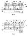
- FIG. 10is a side view of a reconstruction table in accordance with the present invention, with the semiconductor dice of FIG. 9 disposed thereon, arranged in suitable positions by the alignment droplets;
- FIG. 11is a side view of the reconstruction table of FIG. 10 , with an underfill disposed between the semiconductor dice and the reconstruction table;
- FIG. 12is a side view showing one embodiment of a reconstructed wafer, in accordance with the present invention, separated from the reconstruction table;
- FIG. 12Ais a top elevated view of a portion of the reconstructed wafer of FIG. 12 ;
- FIG. 13is a side view depicting the reconstructed wafer of FIG. 12 after a back-grinding process
- FIG. 14is a side view of another embodiment of individual semiconductor dice singulated from the reconstructed wafer of FIG. 13 ;
- FIG. 15is a side view depicting the reconstructed wafer of FIG. 12 with a sacrificial material removed therefrom;
- FIG. 16is a side view depicting the reconstructed wafer of FIG. 15 with a selected replacement filler material filling the void created by the removal of the sacrificial material;
- FIG. 17is a side view depicting the reconstructed wafer embodiment of FIG. 16 attached to an adhesive tape for back-grinding;
- FIG. 18is a side view depicting the reconstructed wafer of FIG. 17 with an underfill material removed therefrom.
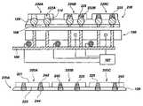
- Reconstruction table 100may be used as a platform for reconstructing a semiconductor wafer.
- One or more wafer reconstruction locations 101may be present on the reconstruction table 100 .
- a reconstruction table 100may be configured for concurrent reconstruction of multiple wafers.
- a temperature control system 102schematically represented by coils, may be present in connection with reconstruction table 100 and used to raise, lower, or maintain a desired temperature of the reconstruction table 100 and surrounding environment.
- temperature control system 102may comprise resistive heating elements, passageways within reconstruction table 100 for circulating fluid of heating or cooling, semiconductor-type heat exchange modules, or other heat exchange systems known in the art.
- one or more sensors 103may be placed within reconstruction table 100 or in contact therewith, sensors 103 being used with a controller 107 for modulating the temperature of reconstruction table 100 in each region or portions thereof.
- Substrate 114may include a fixture plate 110 disposed on the reconstruction table 100 .
- Fixture plate 110has a plurality of patterns of vias 106 that align with the alignment vias 104 when placed on a reconstruction location 101 on reconstruction table 100 .
- Fixture plate 110may be formed of any suitable material, including polymeric materials, crystalline silicon, glass, steel, aluminum or any other suitable material known to those of ordinary skill in the art and desirable for the processing involved. For example, where subsequent processing steps require the lower surface of a wafer to be silicon, a silicon fixture plate 110 may be selected.
- a resulting wafer lacking a fixture plate 110may be removed from the reconstruction table 100 following underfill, the discussion of which follows below.
- the reconstruction location 101may be coated with a compound to aid in the release of a completed wafer therefrom.
- an alignment material 108is delivered in a liquid, gel or other flowable state through at least one alignment via 104 and corresponding via 106 of fixture plate 110 when present, to form at least one alignment droplet 112 at the reconstruction location 101 , atop the fixture plate 110 when present.
- a number of alignment droplets 112will be formed into a desired pattern by the arrangement of a number of alignment vias 104 , as will be explained in more detail further herein.
- a plurality of semiconductor dice 120are shown disposed at the reconstruction location 101 .
- Dice 120may be selected by qualification using wafer probe testing, visual inspection of dice sites on a wafer, or as otherwise desired and known to those of ordinary skill in the art.
- Each die 120may be formed of silicon, gallium arsenide, indium phosphide or other suitable semiconductor material and includes at least one alignment cavity 122 and preferably a pattern thereof, located on a lower non-active surface 123 .
- the die 120will be referred to as having an active surface 121 as the upper surface of the die with an opposite lower non-active surface 123 . It will be understood that such terms are for making relative positions clear and do not limit the invention.
- Alignment cavities 122may be formed in the lower non-active surface 123 of each die 120 using any suitable method for forming vias, cavities, or trenches in semiconductor substrates known to those of ordinary skill in the art.
- the alignment cavities 122may be formed by wet etching, dry etching (and comprise either isotropic etching or anisotropic etching), laser ablation, drilling or boring with a mechanical drill bit, or otherwise as known to those of ordinary skill in the art.
- embodiments utilizing a single alignment cavity 122may be designed and are within the scope of the present invention, it is currently preferred to use a plurality of patterns of alignment cavities 122 on the lower non-active surface 123 , in order to allow the die 120 to be correctly positioned in multiple directions, being the X and Y directions parallel to the plane of reconstruction table 100 , as well as rotationally in the same plane.
- a plurality of patterns of alignment cavities 122 on the lower non-active surface 123in order to allow the die 120 to be correctly positioned in multiple directions, being the X and Y directions parallel to the plane of reconstruction table 100 , as well as rotationally in the same plane.
- one or more parallel rows of alignment cavities 122 or a pattern of alignment cavities 122may be formed on the lower surface of each die. It will be appreciated that any desirable or advantageous arrangement of the alignment cavities 122 on the lower non-active surface 123 of the die 120 may be used and all such patterns and arrangements are within the scope of the present invention.
- Each alignment cavity 122may be formed to any desired depth in the die 120 , so long as it is sufficient to enable the alignment of the die 120 when interacting with a corresponding alignment droplet 112 , as will be explained further herein.
- one or more alignment cavities 122may be used as vias connecting the active surface 121 of the die 120 to the lower non-active surface 123 , increasing throughput by using a single structure for multiple purposes, and enabling novel methods of forming die 120 interconnects or bumped dice for flip-chip applications. Such embodiments will be discussed in more detail further herein.
- a die 120As a die 120 is placed into the reconstruction location 101 by, for example, conventional and suitably programmed pick-and-place equipment, it is roughly aligned with a desired final position in the resulting reconstructed wafer.
- the alignment droplet(s) 112thus make contact with one or more alignment cavities 122 on the lower non-active surface 123 of the die 120 .
- the die 120is then released and the surface tension of the alignment droplets 112 interacts with the similarly patterned alignment cavities 122 to position the die 120 in its final, precise alignment and hold the die 120 in the correct, desired position.
- a plurality of dice 120may be aligned in proper positions with respect to one another to form a reconstructed wafer for further wafer-level processing. Achieving and maintaining proper positioning among the dice is important and required to allow processing of the reconstructed wafer to take place with conventional equipment.
- the alignment droplets 112are then at least partially solidified to retain the dice 120 in the correct positions.
- the temperature of the reconstruction table 100may be raised or lowered to effect an at least partial solidification of a liquid alignment material 108 comprising alignment droplets 112 , solidifying the liquid alignment material 108 and adhering the solidified alignment droplets 112 to the dice 120 .
- the thermoplastic resinwhen using a thermoplastic resin such as the alignment material 108 , the thermoplastic resin may be heated to a melting point by using temperature control system 102 and delivered through alignment vias 104 to form alignment droplets 112 .
- thermoplastic resinmay then be cooled or allowed to cool to a point where the alignment material 108 at least partially solidifies.
- a thermoset resinmay be used as the alignment material 108 , pumped through the alignment vias 104 to form alignment droplets 112 and then heated using temperature control system 102 to solidify.
- a third exemplary alignment material 108may be a liquid epoxy that is heat cured to solidify. With such embodiments, where necessary, the temperature of the alignment vias 104 may be separately maintained at a lower level to prevent solidification therein.
- An additional example of a suitable alignment material 108may be a low melting point metal, such as a tin/lead solder, silver solder or other low melting point metals or alloys.
- the low melting point metalmay be melted and delivered through alignment vias 104 to form alignment droplets 112 and then cooled, or allowed to cool, to solidify.
- a chemical setting agentsuch as the application of a chemical setting agent, the exposure of alignment droplets 112 formed of a photoreactive alignment material 108 to an appropriate wavelength of light, such as a photopolymer that is cured by exposure to radiation (as, for example, polymers that are liquid when heated and gel upon exposure to radiation, such as UV light, x-rays, microwaves, etc.), or any other process known to those of ordinary skill in the art.
- an underfill material 126such as an epoxy, may be disposed under the dice 120 .
- Various dielectric underfill materials 126such as conventional underfill epoxies, are known to those of ordinary skill in the art and any suitable underfill material may be employed to retain the die 120 to the fixture plate 110 or otherwise solidify the positions of dice 120 in the reconstructed wafer.
- a reconstructed wafer 130is formed and may be removed with fixture plate 110 (if present) from the reconstruction table 100 , as shown in FIG. 5 .
- the reconstructed wafer 130then may undergo any desired wafer-level processing to complete the fabrication of the dice 120 or for creation of complete multidie semiconductor assemblies.
- the reconstructed wafer 130may undergo wafer-level testing and burn-in to qualify dice 120 thereof as KGD, although it will be appreciated that any desired wafer-level treatment such as wafer-level rerouting or wafer-level treatments for packaging may be performed on the reconstructed wafer 130 .
- reconstructed wafermeans any reconstructed bulk substrate, including semiconductor dice.
- Such reconstructed wafersmay have any desired shape, including a conventional round wafer shape, which may be desirable for processing with conventional wafer handling and processing equipment.
- Other embodimentsmay produce square or rectangular reconstructed wafers, which may be desirable for use with testing equipment. All such shapes are within the scope of the present invention.
- the reconstructed wafer 130may then be singulated into a number of separate dice 120 , which may be KGD, as previously noted.
- One process for singulationis depicted in FIGS. 6 , 7 and 8 .
- the reconstructed wafer 130is attached to a film of adhesive-coated polymer 132 , as in a conventional wafer back-grinding process, with the active surface 121 of the dice 120 adhered to the adhesive-coated polymer 132 , as depicted in FIG. 6 .
- the reconstructed wafer 130is then back-ground, removing the fixture plate 110 (when present), the underfill material 126 and the alignment droplets 112 .
- the back-grindingmay continue to remove the alignment cavities 122 and the remainder of alignment droplets 112 located therein and any desired portion of the reconstructed wafer 130 thickness, resulting in the structure shown in FIG. 7 , of a plurality of thinned dice 120 attached to the adhesive-coated polymer 132 .
- the individual finished dice 120may then be separated by simply removing the adhesive-coated polymer 132 , as depicted in FIG. 8 .
- any alternative method for wafer singulationknown to those of ordinary skill in the art may be used to separate the dice 120 .
- the reconstructed wafermay be singulated with a conventional wafer saw or by any other suitable technique.
- the foregoing methodthus enables creation of a reconstructed wafer using only dice 120 that have no visible defects, or dice 120 that through probe testing have been determined to be at least functional. Additional changes and refinements may be made to the basic method and all such refinements are within the scope of the present invention.
- Some embodiments of processes in accordance with the present inventionmay be used to form interconnects or other structures as a reconstructed wafer is formed or dice 120 are singulated therefrom. Examples of such processes are depicted in FIGS. 9-18 , as discussed below.
- FIG. 9depicts several different dice 220 A, 220 B and 220 C that may be used in practicing certain embodiments of the present invention.
- Different alignment vias 222 A, 222 B, 222 C treatmentshave been applied to each die 220 A, 220 B and 220 C.
- the alignment vias of die 220 Acomprise at least one via 222 A that passes through the thickness of the entire die, allowing contact between the active surface 221 and the non-active surface 223 therethough.
- a suitable coatingmay be placed on the interior surface of the via 222 A.
- an insulative coatingmay be placed on the via 222 A walls to protect the die 220 A from the inductive effects of a current passing through conductive material later filling the via 222 A.
- a conductive coatingmay be applied to form part of a conductive interconnection structure.
- the alignment vias 222 of die 220 Bsimilarly comprise at least one via 222 B that passes through the thickness of the die 220 B.
- Via 222 Bis partially filled with a selected filler material 225 , such as a sacrificial material or a conductive material that can be in electrical communication with the integrated circuit formed on the active surface 221 of the die 220 B.
- a selected filler material 225such as a sacrificial material or a conductive material that can be in electrical communication with the integrated circuit formed on the active surface 221 of the die 220 B.
- via 222 Bis filled from 1 ⁇ 4 to 3 ⁇ 4 with the selected filler material 225 , although any other suitable partial filling may be used.
- the at least one alignment via 222 C of die 220 Cpasses through the thickness of the die 220 C, but is filled with any suitable selected filler material 225 substantially throughout its depth. It will, of course, be appreciated that the walls of alignment vias 222 B and 222 C may be coated with any desired coatings
- a number of alignment droplets 112are extruded through the reconstruction table 100 , and the dice 220 A, 220 B, 220 C, are disposed thereon, such that the interaction of the surface tension of the alignment droplets 112 aligns dice 220 A, 220 B, 220 C, for exact placement in a reconstructed wafer, as has been discussed previously herein.
- the alignment droplet 112 sizemay be controlled to result in filling the volume of the alignment vias 222 A- 222 C that has not been filled previously with a selected filler material with the alignment droplet 112 .
- an “empty” viasuch as 222 A
- thiscan result in a via filled with the alignment material 108 or a via partially filled with alignment material 108 .
- a partially empty viasuch as 222 B
- thisresults in a via partially filled with selected filler material 225 with the remainder filled by alignment material 108 .
- the material of the alignment material 108is selected to “wet” the filler material 225 , so that the surface tension of alignment droplets 112 is effective to align die 220 C.
- the alignment material 108may be a conductive material, such as a metallic solder, a conductive polymer, or a polymer containing conductive material suspended therein.
- the alignment material 108may comprise a sacrificial material.
- sacrificial materialrefers to any material, or compound, that may be utilized for a specific function in any process or method of the present invention and then be removed at a later stage of such process or method.
- the alignment droplets 112are back-ground from the die 120 , as discussed previously herein, such alignment droplets 112 are considered to be a sacrificial material. Sacrificial materials may be selected to facilitate their removal after use, as will be discussed further herein.
- the alignment droplets 112are then heated, cooled, or otherwise treated to at least partially solidify and an underfill material 126 is disposed underneath the dice 220 A, 220 B, 220 C, and around the solidified alignment droplets 112 , resulting in the structure seen in FIG. 11 .
- the underfill 126may then be removed for processing, as discussed previously herein and depicted in FIG. 12 .
- a plan view of a portion of the reconstructed wafer 230is shown in FIG. 12A .
- the reconstructed wafer 230may undergo any wafer-level processing that is desired as is discussed previously herein. Wafer-level burn-in and testing may even be conducted. Where the alignment material 108 selected is a conductive material and, if present, the selected filler material 225 is also conductive and makes contact with the patterns of the active surface 221 of the die 220 A, 220 B, 220 C, testing and burn-in may be effected by making electrically communicative contact with the solidified alignment material 108 as exposed at the non-active surface 223 of the reconstructed wafer 230 , as through the vias 106 of a fixture plate 110 .
- the reconstructed wafer 230may then be singulated into a plurality of separate dice 220 A, 220 B, 220 C. Similar to that discussed previously herein, one process for doing so is depicted in FIGS. 13 and 14 .
- the reconstructed wafer 230is attached to a length of adhesive-coated polymer 132 , as in a conventional wafer back-grinding process, with the active surfaces 221 of the dice 220 A, 220 B, 220 C, adhered to the adhesive-coated polymer 132 .
- the reconstructed wafer 230is then back-ground, removing the fixture plate 110 (where present), the underfill material 126 and the alignment material 108 or selected filler material 225 that is present in the portion of the dice 220 A, 220 B, 220 C, that are back-ground.
- Each finished die 220 A, 220 B, 220 Ccontains a via 222 A, 222 B, 222 C, across the width thereof that is filled either with the selected filler material 225 or the alignment material 108 .
- the alignment material 108is conductive and is in electrical communication with the active surface 221 of the dice 220 A, 220 B, 220 C
- thisprovides contacts 226 on the non-active surfaces 223 of the dice that may be utilized in mounting the dice 220 A, 220 B, 220 C, in a complete semiconductor package or in an appropriate device.
- Individual finished dice 220 A, 220 B, 220 Cmay be separated by simply removing the adhesive-coated polymer 132 , as depicted in FIG. 14 .
- any alternative method for wafer singulationknown to those of ordinary skill in the art, may be used to separate the dice 220 A, 220 B, 220 C.
- FIGS. 15-18Some additional processing embodiments, in accordance with the principles of the present invention, are depicted in FIGS. 15-18 .
- a reconstructed wafer 230 Ais created as discussed previously herein in connection with FIGS. 9-12 .
- the reconstructed wafermay undergo any desired wafer-level processing procedure.
- the fixture plate 110is removed, mechanically by back-grinding, or by utilizing the fixture plate 110 formed from a material that may be dissolved, or by removing the fixture plate 110 with treatment by a suitable release agent.
- the need for this proceduremay be eliminated by creating the reconstructed wafer 230 A that lacks a fixture plate 110 .
- the alignment droplets 112are thus at least accessible, if not partially exposed, through the underfill material 126 which holds the reconstructed wafer 230 A together.
- the alignment material 108may then be removed from the reconstructed wafer 230 A.
- the selected filler material 225is a sacrificial material, it may also be removed. Removal of the sacrificial material may be accomplished in any manner suitable for the specific sacrificial material at issue. For example, a selective chemical etch may be performed to remove the sacrificial material.
- the temperature of the reconstructed wafer 230 Amay be lowered or raised to reverse the alignment material 108 phase change and allow a sacrificial material that is no longer solid to be removed by application of a vacuum or by a flushing or draining procedure.
- the reconstructed wafer 230 Acontains at least one void 240 in the underfill material 126 that corresponds to a removed alignment droplet 112 and may be connected to an empty, or at least partially empty, alignment via, such as those depicted as 222 A and 222 B in FIG. 15 .
- the vacated volumemay be filled with a selected replacement filler material 242 , as is desired.
- the selected replacement filler material 242may be a conductive metal or alloy, such as tin/lead solder, gold or a conductive polymer or conductively filled polymer to create a conductive structure through the vias 222 A, 222 B, 222 C, and an integral conductive bump 244 on the non-active surface 223 , as depicted in FIG. 16 .
- a conductive metal or alloysuch as tin/lead solder, gold or a conductive polymer or conductively filled polymer to create a conductive structure through the vias 222 A, 222 B, 222 C, and an integral conductive bump 244 on the non-active surface 223 , as depicted in FIG. 16 .
- any desired selected replacement filler material 242may be used.
- the reconstructed wafer 230 Amay then undergo any additional desired wafer-level processing. It may be advantageous to attach the active surface 221 of the reconstructed wafer 230 A to a length of adhesive-coated polymer 132 to protect the active surfaces 221 of the dice 220 A, 220 B, 220 C, as depicted in FIG. 17 . This procedure may occur during processing, or prior to removal of the sacrificial material. Processing of the wafer at this stage may include wafer testing and burn-in of the dice 220 A, 220 B, 220 C, using conductive bumps 244 as contacts.
- the underfill material 126may then be removed from the reconstructed wafer to substantially fully expose the conductive bumps 244 . This may be accomplished in any suitable manner, such as by selectively removing the underfill material 126 through a chemical etch process, or by selecting an underfill material that can be induced to reflow from the reconstructed wafer 230 A under appropriate conditions. Removal of the underfill material results in dice 220 A, 220 B, 220 C, with substantially fully exposed bumps 244 , similar to those depicted in FIG. 18 . Of course, it will be appreciated that some embodiments in which the underfill material is not removed may be utilized and are within the scope of the present invention.
- the individual dice 220 A, 220 B, 220 Cmay be singulated from the reconstructed wafer 230 A. Where the underfill material 126 has been removed, similar to the embodiment depicted in FIG. 18 , this may be accomplished by removing the dice 220 A, 220 B, 220 C, from the adhesive-coated polymer 132 , as has been discussed previously herein. Alternatively, singulation of the reconstructed wafer 230 may be accomplished using wafer sawing techniques. Where adhesive-coated polymer 132 has been applied to the active surface 221 of the reconstructed wafer 230 A, this leaves a protective layer on the active surfaces 221 of the resulting dice 220 A, 220 B, 220 C.
- singulationmay not be effected and the dice 220 A, 220 B, 220 C, may be marketed or used as multidie assemblies.
- an adhesive-coated polymer 132that is susceptible to chemical etching or other non-mechanical severance or removal may be used and such singulation is also within the scope of the present invention.
- reconstructed wafers 230 and 230 Acan be created that may include only known good dice. These reconstructed wafers may then be processed in the same manner as any other wafer, using standard wafer-level processing equipment.
Landscapes
- Engineering & Computer Science (AREA)
- Microelectronics & Electronic Packaging (AREA)
- Power Engineering (AREA)
- Computer Hardware Design (AREA)
- Physics & Mathematics (AREA)
- Condensed Matter Physics & Semiconductors (AREA)
- General Physics & Mathematics (AREA)
- Manufacturing & Machinery (AREA)
- Dicing (AREA)
- Mechanical Treatment Of Semiconductor (AREA)
- Encapsulation Of And Coatings For Semiconductor Or Solid State Devices (AREA)
- Wire Bonding (AREA)
Abstract
Description
Claims (16)
Priority Applications (2)
| Application Number | Priority Date | Filing Date | Title |
|---|---|---|---|
| US11/449,472US7425462B2 (en) | 2003-07-05 | 2006-06-07 | Methods relating to the reconstruction of semiconductor wafers for wafer-level processing |
| US12/200,027US7820459B2 (en) | 2003-07-05 | 2008-08-28 | Methods relating to the reconstruction of semiconductor wafers for wafer level processing including forming of alignment protrusion and removal of alignment material |
Applications Claiming Priority (4)
| Application Number | Priority Date | Filing Date | Title |
|---|---|---|---|
| SG200302784-4 | 2003-07-05 | ||
| SG200302784 | 2003-07-05 | ||
| US10/645,389US7071012B2 (en) | 2003-07-05 | 2003-08-21 | Methods relating to the reconstruction of semiconductor wafers for wafer-level processing |
| US11/449,472US7425462B2 (en) | 2003-07-05 | 2006-06-07 | Methods relating to the reconstruction of semiconductor wafers for wafer-level processing |
Related Parent Applications (1)
| Application Number | Title | Priority Date | Filing Date |
|---|---|---|---|
| US10/645,389DivisionUS7071012B2 (en) | 2003-07-05 | 2003-08-21 | Methods relating to the reconstruction of semiconductor wafers for wafer-level processing |
Related Child Applications (1)
| Application Number | Title | Priority Date | Filing Date |
|---|---|---|---|
| US12/200,027ContinuationUS7820459B2 (en) | 2003-07-05 | 2008-08-28 | Methods relating to the reconstruction of semiconductor wafers for wafer level processing including forming of alignment protrusion and removal of alignment material |
Publications (2)
| Publication Number | Publication Date |
|---|---|
| US20060240582A1 US20060240582A1 (en) | 2006-10-26 |
| US7425462B2true US7425462B2 (en) | 2008-09-16 |
Family
ID=33550644
Family Applications (5)
| Application Number | Title | Priority Date | Filing Date |
|---|---|---|---|
| US10/645,389Expired - Fee RelatedUS7071012B2 (en) | 2003-07-05 | 2003-08-21 | Methods relating to the reconstruction of semiconductor wafers for wafer-level processing |
| US11/196,584Expired - LifetimeUS7190074B2 (en) | 2003-07-05 | 2005-08-02 | Reconstructed semiconductor wafers including alignment droplets contacting alignment vias |
| US11/196,757Expired - LifetimeUS7573006B2 (en) | 2003-07-05 | 2005-08-02 | Apparatus relating to the reconstruction of semiconductor wafers for wafer-level processing |
| US11/449,472Expired - LifetimeUS7425462B2 (en) | 2003-07-05 | 2006-06-07 | Methods relating to the reconstruction of semiconductor wafers for wafer-level processing |
| US12/200,027Expired - Fee RelatedUS7820459B2 (en) | 2003-07-05 | 2008-08-28 | Methods relating to the reconstruction of semiconductor wafers for wafer level processing including forming of alignment protrusion and removal of alignment material |
Family Applications Before (3)
| Application Number | Title | Priority Date | Filing Date |
|---|---|---|---|
| US10/645,389Expired - Fee RelatedUS7071012B2 (en) | 2003-07-05 | 2003-08-21 | Methods relating to the reconstruction of semiconductor wafers for wafer-level processing |
| US11/196,584Expired - LifetimeUS7190074B2 (en) | 2003-07-05 | 2005-08-02 | Reconstructed semiconductor wafers including alignment droplets contacting alignment vias |
| US11/196,757Expired - LifetimeUS7573006B2 (en) | 2003-07-05 | 2005-08-02 | Apparatus relating to the reconstruction of semiconductor wafers for wafer-level processing |
Family Applications After (1)
| Application Number | Title | Priority Date | Filing Date |
|---|---|---|---|
| US12/200,027Expired - Fee RelatedUS7820459B2 (en) | 2003-07-05 | 2008-08-28 | Methods relating to the reconstruction of semiconductor wafers for wafer level processing including forming of alignment protrusion and removal of alignment material |
Country Status (1)
| Country | Link |
|---|---|
| US (5) | US7071012B2 (en) |
Cited By (1)
| Publication number | Priority date | Publication date | Assignee | Title |
|---|---|---|---|---|
| US20080132035A1 (en)* | 2006-11-30 | 2008-06-05 | Disco Corporation | Method of processing wafer |
Families Citing this family (16)
| Publication number | Priority date | Publication date | Assignee | Title |
|---|---|---|---|---|
| US6297548B1 (en) | 1998-06-30 | 2001-10-02 | Micron Technology, Inc. | Stackable ceramic FBGA for high thermal applications |
| US7071012B2 (en)* | 2003-07-05 | 2006-07-04 | Micron Technology, Inc. | Methods relating to the reconstruction of semiconductor wafers for wafer-level processing |
| US7064010B2 (en)* | 2003-10-20 | 2006-06-20 | Micron Technology, Inc. | Methods of coating and singulating wafers |
| US7838331B2 (en)* | 2005-11-16 | 2010-11-23 | Denso Corporation | Method for dicing semiconductor substrate |
| TWI307406B (en)* | 2006-07-06 | 2009-03-11 | Au Optronics Corp | Misalignment detection devices |
| US20080061309A1 (en)* | 2006-07-21 | 2008-03-13 | Young Sir Chung | Semiconductor device with under-filled heat extractor |
| US7666321B2 (en)* | 2006-09-26 | 2010-02-23 | United Microelectronics Corp. | Method for decapsulating package |
| US7844099B2 (en)* | 2006-11-15 | 2010-11-30 | International Business Machines Corporation | Inspection method for protecting image sensor devices with front surface protection |
| US20080113456A1 (en)* | 2006-11-15 | 2008-05-15 | International Business Machines Corporation | Process for protecting image sensor wafers from front surface damage and contamination |
| US7977778B2 (en)* | 2007-05-04 | 2011-07-12 | Stats Chippac Ltd. | Integrated circuit package system with interference-fit feature |
| US7696064B2 (en)* | 2007-10-11 | 2010-04-13 | Skyworks Solutions, Inc. | Methods for forming a through via |
| SG142321A1 (en) | 2008-04-24 | 2009-11-26 | Micron Technology Inc | Pre-encapsulated cavity interposer |
| US8004296B2 (en)* | 2008-08-19 | 2011-08-23 | Centipede Systems, Inc. | Probe head apparatus for testing semiconductors |
| US9093448B2 (en) | 2008-11-25 | 2015-07-28 | Lord Corporation | Methods for protecting a die surface with photocurable materials |
| KR101641608B1 (en)* | 2008-11-25 | 2016-07-21 | 로오드 코포레이션 | Methods for protecting a die surface with photocurable materials |
| KR102736227B1 (en) | 2016-07-29 | 2024-12-03 | 삼성전자주식회사 | Circuit board and semiconductor package |
Citations (16)
| Publication number | Priority date | Publication date | Assignee | Title |
|---|---|---|---|---|
| US4499655A (en) | 1981-03-18 | 1985-02-19 | General Electric Company | Method for making alignment-enhancing feed-through conductors for stackable silicon-on-sapphire |
| US5224265A (en) | 1991-10-29 | 1993-07-06 | International Business Machines Corporation | Fabrication of discrete thin film wiring structures |
| US5634267A (en) | 1991-06-04 | 1997-06-03 | Micron Technology, Inc. | Method and apparatus for manufacturing known good semiconductor die |
| US5637536A (en) | 1993-08-13 | 1997-06-10 | Thomson-Csf | Method for interconnecting semiconductor chips in three dimensions, and component resulting therefrom |
| US6013534A (en) | 1997-07-25 | 2000-01-11 | The United States Of America As Represented By The National Security Agency | Method of thinning integrated circuits received in die form |
| US6053395A (en) | 1997-08-06 | 2000-04-25 | Nec Corporation | Method of flip-chip bonding between a chip element and a wafer-board |
| US6064221A (en) | 1996-01-02 | 2000-05-16 | Micron Technology, Inc. | Method of temporarily securing a die to a burn-in carrier |
| US6219908B1 (en) | 1991-06-04 | 2001-04-24 | Micron Technology, Inc. | Method and apparatus for manufacturing known good semiconductor die |
| US6245595B1 (en) | 1999-07-22 | 2001-06-12 | National Semiconductor Corporation | Techniques for wafer level molding of underfill encapsulant |
| US6258609B1 (en) | 1996-09-30 | 2001-07-10 | Micron Technology, Inc. | Method and system for making known good semiconductor dice |
| US6275051B1 (en) | 1997-12-29 | 2001-08-14 | International Business Machines Corporation | Segmented architecture for wafer test and burn-in |
| US20020066523A1 (en) | 2000-12-05 | 2002-06-06 | Sundstrom Lance L. | Attaching devices using polymers |
| US6444576B1 (en) | 2000-06-16 | 2002-09-03 | Chartered Semiconductor Manufacturing, Ltd. | Three dimensional IC package module |
| US20030017687A1 (en)* | 2000-08-31 | 2003-01-23 | Micron Technology, Inc. | Method for filling a wafer through-VIA with a conductive material |
| US6610560B2 (en) | 2001-05-11 | 2003-08-26 | Siliconware Precision Industries Co., Ltd. | Chip-on-chip based multi-chip module with molded underfill and method of fabricating the same |
| US20030164555A1 (en) | 2002-03-01 | 2003-09-04 | Tong Quinn K. | B-stageable underfill encapsulant and method for its application |
Family Cites Families (7)
| Publication number | Priority date | Publication date | Assignee | Title |
|---|---|---|---|---|
| JP2658672B2 (en)* | 1991-10-11 | 1997-09-30 | 日本電気株式会社 | I/O pin repair structure and repair method |
| JP2819523B2 (en)* | 1992-10-09 | 1998-10-30 | インターナショナル・ビジネス・マシーンズ・コーポレイション | Printed wiring board and method of manufacturing the same |
| US6711812B1 (en)* | 1999-04-13 | 2004-03-30 | Unicap Electronics Industrial Corporation | Method of making metal core substrate printed circuit wiring board enabling thermally enhanced ball grid array (BGA) packages |
| US7007378B2 (en)* | 1999-06-24 | 2006-03-07 | International Business Machines Corporation | Process for manufacturing a printed wiring board |
| US6622907B2 (en)* | 2002-02-19 | 2003-09-23 | International Business Machines Corporation | Sacrificial seed layer process for forming C4 solder bumps |
| JP2003338587A (en)* | 2002-05-21 | 2003-11-28 | Hitachi Ltd | Semiconductor device and manufacturing method thereof |
| US7071012B2 (en)* | 2003-07-05 | 2006-07-04 | Micron Technology, Inc. | Methods relating to the reconstruction of semiconductor wafers for wafer-level processing |
- 2003
- 2003-08-21USUS10/645,389patent/US7071012B2/ennot_activeExpired - Fee Related
- 2005
- 2005-08-02USUS11/196,584patent/US7190074B2/ennot_activeExpired - Lifetime
- 2005-08-02USUS11/196,757patent/US7573006B2/ennot_activeExpired - Lifetime
- 2006
- 2006-06-07USUS11/449,472patent/US7425462B2/ennot_activeExpired - Lifetime
- 2008
- 2008-08-28USUS12/200,027patent/US7820459B2/ennot_activeExpired - Fee Related
Patent Citations (16)
| Publication number | Priority date | Publication date | Assignee | Title |
|---|---|---|---|---|
| US4499655A (en) | 1981-03-18 | 1985-02-19 | General Electric Company | Method for making alignment-enhancing feed-through conductors for stackable silicon-on-sapphire |
| US5634267A (en) | 1991-06-04 | 1997-06-03 | Micron Technology, Inc. | Method and apparatus for manufacturing known good semiconductor die |
| US6219908B1 (en) | 1991-06-04 | 2001-04-24 | Micron Technology, Inc. | Method and apparatus for manufacturing known good semiconductor die |
| US5224265A (en) | 1991-10-29 | 1993-07-06 | International Business Machines Corporation | Fabrication of discrete thin film wiring structures |
| US5637536A (en) | 1993-08-13 | 1997-06-10 | Thomson-Csf | Method for interconnecting semiconductor chips in three dimensions, and component resulting therefrom |
| US6064221A (en) | 1996-01-02 | 2000-05-16 | Micron Technology, Inc. | Method of temporarily securing a die to a burn-in carrier |
| US6258609B1 (en) | 1996-09-30 | 2001-07-10 | Micron Technology, Inc. | Method and system for making known good semiconductor dice |
| US6013534A (en) | 1997-07-25 | 2000-01-11 | The United States Of America As Represented By The National Security Agency | Method of thinning integrated circuits received in die form |
| US6053395A (en) | 1997-08-06 | 2000-04-25 | Nec Corporation | Method of flip-chip bonding between a chip element and a wafer-board |
| US6275051B1 (en) | 1997-12-29 | 2001-08-14 | International Business Machines Corporation | Segmented architecture for wafer test and burn-in |
| US6245595B1 (en) | 1999-07-22 | 2001-06-12 | National Semiconductor Corporation | Techniques for wafer level molding of underfill encapsulant |
| US6444576B1 (en) | 2000-06-16 | 2002-09-03 | Chartered Semiconductor Manufacturing, Ltd. | Three dimensional IC package module |
| US20030017687A1 (en)* | 2000-08-31 | 2003-01-23 | Micron Technology, Inc. | Method for filling a wafer through-VIA with a conductive material |
| US20020066523A1 (en) | 2000-12-05 | 2002-06-06 | Sundstrom Lance L. | Attaching devices using polymers |
| US6610560B2 (en) | 2001-05-11 | 2003-08-26 | Siliconware Precision Industries Co., Ltd. | Chip-on-chip based multi-chip module with molded underfill and method of fabricating the same |
| US20030164555A1 (en) | 2002-03-01 | 2003-09-04 | Tong Quinn K. | B-stageable underfill encapsulant and method for its application |
Cited By (2)
| Publication number | Priority date | Publication date | Assignee | Title |
|---|---|---|---|---|
| US20080132035A1 (en)* | 2006-11-30 | 2008-06-05 | Disco Corporation | Method of processing wafer |
| US7662666B2 (en)* | 2006-11-30 | 2010-02-16 | Disco Corporation | Method of processing wafer |
Also Published As
| Publication number | Publication date |
|---|---|
| US20050263517A1 (en) | 2005-12-01 |
| US7573006B2 (en) | 2009-08-11 |
| US20050275116A1 (en) | 2005-12-15 |
| US7190074B2 (en) | 2007-03-13 |
| US20050003575A1 (en) | 2005-01-06 |
| US20080311685A1 (en) | 2008-12-18 |
| US20060240582A1 (en) | 2006-10-26 |
| US7820459B2 (en) | 2010-10-26 |
| US7071012B2 (en) | 2006-07-04 |
Similar Documents
| Publication | Publication Date | Title |
|---|---|---|
| US7425462B2 (en) | Methods relating to the reconstruction of semiconductor wafers for wafer-level processing | |
| US7043830B2 (en) | Method of forming conductive bumps | |
| US8048781B2 (en) | Methods and systems for packaging integrated circuits | |
| KR100257420B1 (en) | Systems interconnected by bumps of joining material | |
| DE102015105990B4 (en) | Semiconductor component and manufacturing process | |
| US6861345B2 (en) | Method of disposing conductive bumps onto a semiconductor device | |
| TWI459505B (en) | Electrical interconnect structure and method | |
| US7208410B2 (en) | Methods relating to forming interconnects | |
| JP2001094005A (en) | Semiconductor device and method for producing it | |
| JPH0766242A (en) | Electronic element assembly, and reprocessing method thereof | |
| JP2002093830A (en) | Manufacturing method of chip-like electronic component, and manufacturing method of pseudo-wafer used for the manufacturing method | |
| US12394696B2 (en) | Package structure including an array of copper pillars and methods of forming the same | |
| JP2002353347A (en) | Semiconductor device and manufacturing method thereof | |
| US20230395479A1 (en) | Dual-underfill encapsulation for packaging and methods of forming the same | |
| US10679954B2 (en) | Integrated circuit system with carrier construction configuration and method of manufacture thereof | |
| TW202312408A (en) | Fan-out package | |
| DE102009033442A1 (en) | Semiconductor device with a copolymer layer | |
| JP2004128286A (en) | Chip-like electronic component and manufacturing method thereof, pseudo wafer used for the manufacturing and manufacturing method thereof, and mounting structure | |
| DE102019118480B4 (en) | INTEGRATED CIRCUIT PACKAGE AND METHOD | |
| JP2002124527A (en) | Method for manufacturing chip electronic component and method for manufacturing dummy wafer used therefor | |
| CN222720407U (en) | Semiconductor package | |
| US20240321758A1 (en) | Deformation-resistant interposer for a local silicon interconnect and methods for forming the same | |
| US7485493B2 (en) | Singulating surface-mountable semiconductor devices and fitting external contacts to said devices | |
| JP3699915B2 (en) | Manufacturing method of semiconductor device | |
| JP2003152134A (en) | Method for manufacturing chip electronic component, and method for manufacturing artificial wafer for use therein |
Legal Events
| Date | Code | Title | Description |
|---|---|---|---|
| FEPP | Fee payment procedure | Free format text:PAYOR NUMBER ASSIGNED (ORIGINAL EVENT CODE: ASPN); ENTITY STATUS OF PATENT OWNER: LARGE ENTITY | |
| STCF | Information on status: patent grant | Free format text:PATENTED CASE | |
| CC | Certificate of correction | ||
| FPAY | Fee payment | Year of fee payment:4 | |
| FPAY | Fee payment | Year of fee payment:8 | |
| AS | Assignment | Owner name:U.S. BANK NATIONAL ASSOCIATION, AS COLLATERAL AGENT, CALIFORNIA Free format text:SECURITY INTEREST;ASSIGNOR:MICRON TECHNOLOGY, INC.;REEL/FRAME:038669/0001 Effective date:20160426 Owner name:U.S. BANK NATIONAL ASSOCIATION, AS COLLATERAL AGEN Free format text:SECURITY INTEREST;ASSIGNOR:MICRON TECHNOLOGY, INC.;REEL/FRAME:038669/0001 Effective date:20160426 | |
| AS | Assignment | Owner name:MORGAN STANLEY SENIOR FUNDING, INC., AS COLLATERAL AGENT, MARYLAND Free format text:PATENT SECURITY AGREEMENT;ASSIGNOR:MICRON TECHNOLOGY, INC.;REEL/FRAME:038954/0001 Effective date:20160426 Owner name:MORGAN STANLEY SENIOR FUNDING, INC., AS COLLATERAL Free format text:PATENT SECURITY AGREEMENT;ASSIGNOR:MICRON TECHNOLOGY, INC.;REEL/FRAME:038954/0001 Effective date:20160426 | |
| AS | Assignment | Owner name:U.S. BANK NATIONAL ASSOCIATION, AS COLLATERAL AGENT, CALIFORNIA Free format text:CORRECTIVE ASSIGNMENT TO CORRECT THE REPLACE ERRONEOUSLY FILED PATENT #7358718 WITH THE CORRECT PATENT #7358178 PREVIOUSLY RECORDED ON REEL 038669 FRAME 0001. ASSIGNOR(S) HEREBY CONFIRMS THE SECURITY INTEREST;ASSIGNOR:MICRON TECHNOLOGY, INC.;REEL/FRAME:043079/0001 Effective date:20160426 Owner name:U.S. BANK NATIONAL ASSOCIATION, AS COLLATERAL AGEN Free format text:CORRECTIVE ASSIGNMENT TO CORRECT THE REPLACE ERRONEOUSLY FILED PATENT #7358718 WITH THE CORRECT PATENT #7358178 PREVIOUSLY RECORDED ON REEL 038669 FRAME 0001. ASSIGNOR(S) HEREBY CONFIRMS THE SECURITY INTEREST;ASSIGNOR:MICRON TECHNOLOGY, INC.;REEL/FRAME:043079/0001 Effective date:20160426 | |
| AS | Assignment | Owner name:JPMORGAN CHASE BANK, N.A., AS COLLATERAL AGENT, ILLINOIS Free format text:SECURITY INTEREST;ASSIGNORS:MICRON TECHNOLOGY, INC.;MICRON SEMICONDUCTOR PRODUCTS, INC.;REEL/FRAME:047540/0001 Effective date:20180703 Owner name:JPMORGAN CHASE BANK, N.A., AS COLLATERAL AGENT, IL Free format text:SECURITY INTEREST;ASSIGNORS:MICRON TECHNOLOGY, INC.;MICRON SEMICONDUCTOR PRODUCTS, INC.;REEL/FRAME:047540/0001 Effective date:20180703 | |
| AS | Assignment | Owner name:MICRON TECHNOLOGY, INC., IDAHO Free format text:RELEASE BY SECURED PARTY;ASSIGNOR:U.S. BANK NATIONAL ASSOCIATION, AS COLLATERAL AGENT;REEL/FRAME:047243/0001 Effective date:20180629 | |
| AS | Assignment | Owner name:MICRON TECHNOLOGY, INC., IDAHO Free format text:RELEASE BY SECURED PARTY;ASSIGNOR:MORGAN STANLEY SENIOR FUNDING, INC., AS COLLATERAL AGENT;REEL/FRAME:050937/0001 Effective date:20190731 | |
| AS | Assignment | Owner name:MICRON SEMICONDUCTOR PRODUCTS, INC., IDAHO Free format text:RELEASE BY SECURED PARTY;ASSIGNOR:JPMORGAN CHASE BANK, N.A., AS COLLATERAL AGENT;REEL/FRAME:051028/0001 Effective date:20190731 Owner name:MICRON TECHNOLOGY, INC., IDAHO Free format text:RELEASE BY SECURED PARTY;ASSIGNOR:JPMORGAN CHASE BANK, N.A., AS COLLATERAL AGENT;REEL/FRAME:051028/0001 Effective date:20190731 | |
| MAFP | Maintenance fee payment | Free format text:PAYMENT OF MAINTENANCE FEE, 12TH YEAR, LARGE ENTITY (ORIGINAL EVENT CODE: M1553); ENTITY STATUS OF PATENT OWNER: LARGE ENTITY Year of fee payment:12 |