US7423606B2 - Multi-frequency RFID apparatus and methods of reading RFID tags - Google Patents
Multi-frequency RFID apparatus and methods of reading RFID tagsDownload PDFInfo
- Publication number
- US7423606B2 US7423606B2US10/957,529US95752904AUS7423606B2US 7423606 B2US7423606 B2US 7423606B2US 95752904 AUS95752904 AUS 95752904AUS 7423606 B2US7423606 B2US 7423606B2
- Authority
- US
- United States
- Prior art keywords
- antenna
- frequency
- field
- antenna element
- portable
- Prior art date
- Legal status (The legal status is an assumption and is not a legal conclusion. Google has not performed a legal analysis and makes no representation as to the accuracy of the status listed.)
- Active, expires
Links
Images


Classifications
- H—ELECTRICITY
- H01—ELECTRIC ELEMENTS
- H01Q—ANTENNAS, i.e. RADIO AERIALS
- H01Q1/00—Details of, or arrangements associated with, antennas
- H01Q1/12—Supports; Mounting means
- H01Q1/22—Supports; Mounting means by structural association with other equipment or articles
- H01Q1/2208—Supports; Mounting means by structural association with other equipment or articles associated with components used in interrogation type services, i.e. in systems for information exchange between an interrogator/reader and a tag/transponder, e.g. in Radio Frequency Identification [RFID] systems
- H01Q1/2216—Supports; Mounting means by structural association with other equipment or articles associated with components used in interrogation type services, i.e. in systems for information exchange between an interrogator/reader and a tag/transponder, e.g. in Radio Frequency Identification [RFID] systems used in interrogator/reader equipment
- G—PHYSICS
- G06—COMPUTING OR CALCULATING; COUNTING
- G06K—GRAPHICAL DATA READING; PRESENTATION OF DATA; RECORD CARRIERS; HANDLING RECORD CARRIERS
- G06K7/00—Methods or arrangements for sensing record carriers, e.g. for reading patterns
- G06K7/0008—General problems related to the reading of electronic memory record carriers, independent of its reading method, e.g. power transfer
- H—ELECTRICITY
- H01—ELECTRIC ELEMENTS
- H01Q—ANTENNAS, i.e. RADIO AERIALS
- H01Q21/00—Antenna arrays or systems
- H01Q21/28—Combinations of substantially independent non-interacting antenna units or systems
- H—ELECTRICITY
- H01—ELECTRIC ELEMENTS
- H01Q—ANTENNAS, i.e. RADIO AERIALS
- H01Q21/00—Antenna arrays or systems
- H01Q21/30—Combinations of separate antenna units operating in different wavebands and connected to a common feeder system
Definitions
- the present inventiongenerally relates to a multi-frequency antenna, and more particularly relates to a directional antenna array for radio frequency identification (RFID).
- RFIDradio frequency identification
- Yagi-Uda antennaswere originally described in the English language in an article written by H. Yagi (See H. Yagi, “Beam Transmission of the Ultra Short Waves,” Proc. IRE. Vol. 16, pp. 715-741, June 1928). These directional dipole antennas, which are commonly referred to as Yagi antennas, have been used for many years and in many applications. For example, the Yagi antenna has been used for reception of television signals, point-to-point communications and other electronics applications.
- the basic Yagi antennatypically includes a driven element, usually a half-wave dipole, which is driven from a source of electromagnetic energy or drives a sink of electromagnetic energy.
- the antennaalso typically includes non-driven or parasitic elements that are arrayed with the driven element. These non-driven or parasitic elements generally comprise a reflector element on one side of the driven element and at least one director element on the other side of the driven element (i.e., the driven element is interposed between the reflector element and the director element).
- the driven element, reflector element and director elementare usually positioned in a spaced relationship along an antenna axis with the director element or elements extending in a transmission or reception direction from the driven element.
- the length of the driven, reflector and director elements and the separations between these antenna elementsspecify the maximum Effective Isotropic Radiated Power (EIRP) of the antenna system (i.e., directive gain) in the antenna system's bore site direction.
- EIRPEffective Isotropic Radiated Power
- antenna designsreflect the desirability of low profile, directional antenna configurations that can conform to any number of shapes for a mobile or portable unit while providing highly directional antenna patterns, such as those achievable with the Yagi antenna.
- current trends in antenna designsreflect the desirability of the antenna to maintain structural shape and integrity after application of an external force, such as a surface impact.
- Such antenna designsare particularly desirable in portable or hand-held devices such as cellular telephones, satellite telephones and contactless interrogators of Automatic Identification (Auto ID) systems, such as Radio Frequency Identification (RFID) interrogators of RFID systems.
- Auto IDAutomatic Identification
- RFIDRadio Frequency Identification
- RFID systemsmay include different tags with various frequency range response. For example, some RFID tags may be categorized as near-field tags or far-field tags based on a corresponding frequency designation for such tags. Additionally, RFID tags may operate in different frequencies.
- One design consideration for RFID systemsis that an RFID antenna used for reading such tags generally has satisfactory reading operation when the antenna size is physically large.
- Another design consideration for RFID systemsis that with hand-held and hands-free RFID readers incorporating RFID antennas, a minimized antenna size is generally desired for portability.
- An additional concernis that a closer proximity of the RFID antenna to a part of a human body tends to degrade performance of the antenna.
- a portable/handheld devicefor radio frequency identification (RFID) and methods of reading inductively coupled radio frequency identification (RFID) tags.
- a portable/handheld deviceincludes a processing module configured to selectively operate a reading mode selected from a far-field mode and a near-field mode, and a directional antenna array coupled to the processing module.
- the directional antenna arrayincludes a first antenna element configured to radiate electromagnetic (EM) radiation in a far-field, and a second antenna element coupled to the first antenna element.
- the second antenna elementis configured to radiate EM radiation in a near-field and includes an antenna transducer configured to selectively cancel far-field EM radiation from the first antenna element.
- a multi-frequency radio frequency identification (RFID) devicehaving a processor configured to scan frequency bands for RFID tags and select a reading mode frequency band based on the scanned frequency bands, a switch coupled to the processor, a first antenna element coupled to the processor, and a second antenna element coupled to the first antenna element.
- the switchis configured to select at least one reading mode frequency band.
- the first antenna elementis configured to radiate electromagnetic (EM) radiation in a far-field.
- the second antenna elementis configured to radiate EM radiation in a near-field and includes an antenna transducer configured to selectively cancel far-field EM radiation from the first antenna element.
- One of the first antenna element and the second antenna elementis further configured to resonate at the at least one reading mode frequency band.
- a method of reading inductively coupled radio frequency identification (RFID) tagshaving the steps of scanning at least one frequency band to detect a RFID tag, and selectively radiating an electromagnetic (EM) field of at least one of a near-field EM field and a far-field EM field based on the detected RFID tag.
- RFIDradio frequency identification
- FIG. 1a planar view of a directional antenna array in accordance with an exemplary embodiment of the present invention
- FIG. 2is a planar view of a directional antenna array with parasitic elements in addition to the parasitic elements illustrated in FIG. 1 ;
- FIG. 3is a first example of a non-planar folded configuration of the directional antenna array of FIG. 1 in accordance with an exemplary embodiment of the present invention
- FIG. 4is a second example of a non-planar folded configuration of the directional antenna array of FIG. 1 in accordance with an exemplary embodiment of the present invention
- FIG. 5is a balun structure for the directional antenna array of FIG. 1 in accordance with an exemplary embodiment of the present invention
- FIG. 6is the directional antenna array of FIG. 3 with an elastomer cover in accordance with a first exemplary embodiment of the present invention
- FIG. 7is the directional antenna array of FIG. 1 with apertures
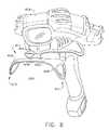
- FIG. 8is a portable/handheld device having the directional antenna array of FIG. 6 in accordance with a first exemplary embodiment of the present invention
- FIG. 9is a directional antenna array with an elastomer cover in accordance with a second exemplary embodiment of the present invention.
- FIG. 10is a portable/handheld device having the directional antenna array of FIG. 9 in accordance with a second exemplary embodiment of the present invention.
- FIG. 11is a flow diagram of a method of reading inductively coupled radio frequency identification tags in accordance with an exemplary embodiment of the present invention.
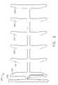
- the directional antenna array 100includes a driven element 102 and at least one (1) parasitic element or director element 104 , and may include a second parasitic element or reflector element 106 in addition to the director element 104 in one exemplary embodiment. While only two parasitic elements (i.e., director element 104 and reflector element 106 ) are shown in FIG. 1 in addition to the driven element 102 , any number of parasitic elements can be provided in accordance with an exemplary embodiment of the present invention. For example, a directional antenna array 200 is shown in FIG.
- parasitic elements( 202 , 204 , 206 , 208 ), which can be one or more additional director or reflector elements in addition to the director element 104 and reflector element 106 as shown in FIG. 1 .
- parasitic elements202 , 204 , 206 , 208
- Examples of other exemplary embodimentsinclude but are not limited to the directional antenna array 100 having: a driven element and a reflector element; a driven element and a director element; a driven element and multiple reflectors; a driven element and multiple directors; and, a driven element with a combination of one or more director elements and reflector elements.
- these one or more additional director or reflector elementscan be in-plane elements or out-of-plane elements, such as a trigonal reflector system having a first reflector positioned above and a second reflector positioned below a third reflector.
- the driven element 102may be the equivalent of a center-fed, half-wave dipole antenna in one exemplary embodiment.
- the director element 104is positioned on one side of the driven element 102 and connected with a boom 108 and the reflector element 106 is positioned on the other side of the director element 102 and connected with another boom 110 such that the driven element 102 is interposed between the director element 104 and the reflector element 106 .
- the director element 102 and the reflector element 106may be positioned in at least a substantially parallel relationship with respect to the driven element 102 and may preferably be positioned in a parallel relationship with respect to the driven element 102 .
- the directional antenna array 100is a Yagi antenna. Accordingly, as known to those of ordinary skill in the art, the design of the directional antenna array 100 involves a selection of parameters of the driven element 102 , director element 104 and/or reflector element 106 and other parameters of additional parasitic elements of the directional antenna array 100 if such elements are present.
- the design of the directional antenna arraycan include selection of spacing between the elements (e.g., spacing (S dir1 ) 112 between the driven element 102 and the director element 104 and spacing (S ref ) 114 between the driven element 102 and the reflector element 106 ), element lengths (e.g., driven element length (L dri ) 116 , director element length (L dir1 ) 118 and reflector element length (L ref ) 120 ), element widths, which as used herein shall include element diameters (e.g., driven element width (W dri ) 122 , director element width (W dir1 ) 124 and reflector element width (W ref ) 126 ).
- spacing (S dir1 ) 112 between the driven element 102 and the director element 104 and spacing (S ref ) 114 between the driven element 102 and the reflector element 106e.g., spacing (S dir1 ) 112 between the driven element 102 and the director element 104 and spacing (S ref )
- the element shapesi.e., round, square, triangular, pentagonal, hexagonal, etc.
- the driven element length (L dri ) 116the reflector element length (L ref ) 120
- the director element length (L dir ) 118the director element spacing (S dir1 ) 112 and the reflector element spacing (S ref ) 114 are selected in accordance with the electrical resonant frequencies of the elements in accordance with techniques known to those of ordinary skill in the art.
- the parameters of the directional antenna array 100are selected such that the electrical frequency of resonance of the director element 104 is preferably greater than the free-space wavelength and the electrical frequency of resonance of the reflector element 106 is less than the free-space wavelength.
- an exemplary boom width (W b1 ) 128 and length and spacing of the driven element 102 , director element 104 and reflector element 106 for a frequency range of approximately nine hundred and two megahertz (902 MHz) to about nine hundred and twenty-eight megahertz (928 MHz)is provided in Table 1.
- the illustrative example presented in Table 1, and other directional antenna arrays designed in accordance with the present inventionis preferably formed of a monolithic material having a thickness that is greater than about one skin depth at an operating frequency of the directional antenna array 100 .
- the monolithic materialcan be any number of materials such as spring steel, beryllium copper, stainless steel or a combination thereof, and the monolithic material preferably can have a resistivity that is greater than about 0.1 ⁇ 10 ⁇ 6 ohms-meter, preferably a resistivity that is greater than 0.2 ⁇ 10 ⁇ 6 ohms-meter, more preferably greater than 0.4 ⁇ 10 ⁇ 6 ohms-meter, even more preferably greater than 0.8 ⁇ 10 ⁇ 6 ohms-meter, and most preferably greater than 1.0 ⁇ 10 ⁇ 6 ohms-meter and 2.0 ⁇ 10 ⁇ 6 ohms-meter.
- the directional antenna array with the dimensions illustratively presented in Table 1can be formed with a thickness of about one-sixteenth ( 1/16) inch FR-10 P.C. Board (PCB) and a two thousandths (0.002) inch copper tape formed on at least one side of the PCB.
- PCBP.C. Board
- a ferrite antenna 134that is effective at lower frequencies such as 13.56 MHz or 135 kHz, may be mounted or otherwise coupled near a center of the director element 104 .
- the ferrite antenna 134may be insulated, such as with a sheet of Kaptan tape or other electrical insulating material, and coupled with a coaxial cable routed along the boom 108 .
- the ferrite antenna 134is oriented such that a major axis of the ferrite antenna 134 is substantially parallel with the longest dimension of the director element 104 as best shown in FIG. 1 .
- a cross-over networkmay be installed with the ferrite antenna 134 such that a single coaxial cable feeds the directional antenna array 100 .
- one output of the cross-over networkcan feed the Yagi antenna (e.g., at about 915 MHz), and another output of the cross-over network can feed the ferrite antenna (e.g., at about 13.56 MHz or about 135 KHz).
- coaxial cablesmay be used for coupling various antenna elements or components, a variety of different RF transmission line types may be used including, but not limited to, strip lines, micro strips, twin leads, flat plate lines, triaxials, co-planar wave guides, wave guides (e.g., rectangular, square, oval, round, etc.), fin lines, and trough lines.
- an array of ferrite antenna elementsmay also be configured.
- multiple ferrite rodsmay be located near the driven element 102 and the reflector 106 as an “end-fire” array.
- an “end-fire” array of 915 MHz ferrite antenna elementsis suited to provide vertical polarization while minimizing any increase in the vertical dimension of the directional antenna array 100 .
- a slot antennamay be integrated with the directional antenna array 100 as described in greater detail hereinbelow.
- a longitudinal slot or an array of slots that are responsive to 2.45 GHz or 5.6 GHZmay be formed in the director element 104 or the boom 108 , or in any of the other elements 102 , 106 , of the directional antenna array 100 .
- the slot antenna element or an array of slot antenna elementscan be coupled with separate coaxial cables that are routed along the boom 108 of the Yagi antenna, or the elements of the Yagi antenna, with separate transmission lines to the elements, or coupled with a cross-over network.
- the multiple slotted elements operating at 2.45 GHz or 5.6 GHzmay be used to increase antenna directivity or for electronic beam steering of the radiated signal on such frequencies.
- the 2.45 GHz and 5.6 GHz radiating elementsare described herein as slot radiators of the Yagi antenna, for example in various locations of a sheet metal, other types of radiating elements that are effective on such frequencies may also be used.
- monopoles, dipoles, folded dipoles, half-folded dipoles, printed circuit patch antennas, printed inverted “F” antennas (PIFA), and the likemay be applied to the Yagi sheet metal.
- the Yagi antennamay be formed of other materials aside from sheet metal and of other configurations, such as metallic tubing (e.g., round, square, triangular, etc.), plastic, or other fibrous materials with a metallic coating (e.g., such that the RF “skin effect” creates a solid appearance).
- the Yagi elementsmay be configured as a loop, triangle, square, or the like.
- the electronic performance of a “loop” Yagi elementis substantially similar to a conventional dipole type Yagi element.
- Alternative element configurationsmay be selected for non-electronic performance considerations such as mechanical strength and immunity to water droplet (e.g., rain) de-tuning. In the latter case, water droplets tend to fall to a lower center of the loops such that added capacitance from the water droplets typically does not de-tune the element.
- the physical size of the slot antennamay be minimized using dielectric loading or magnetic loading as may be appreciated by those of skill in the art.
- the slot antennamay also be constructed to be responsive to a desired frequency range based in part on the length of the longitudinal slot as well as the corresponding length of the director element.
- an LC (inductance-capacitance) matching network coupled to the slot antennacan supply the resonance, at the antenna or through a feed line, at a frequency of operation.
- the driven element 102can be formed into a non-planar folded configuration.
- the distal ends ( 302 , 304 ) of the driven element 102are folded to provide an angle of about ninety degrees (90°) with respect to the boom 108 to form the non-planar folded configuration 300 as shown in FIG. 3 .
- another non-planar configuration 400can be formed by continuing to fold the distal ends ( 302 , 304 ) of the driven element 102 until such ends are substantially adjacent and preferably directly under the boom 108 as shown in FIG.
- the director element 102 and/or reflector element 104can be folded in a manner that is similar or the same as the driven element as shown in FIG. 3 , in a different manner that is not similar to the driven element as shown in FIG. 4 , or in any other manner to provide specific antenna characteristics or antenna aesthetics.
- the elements of the directional antenna array 100may be constructed from printed coil structures.
- an outer dimension, such as a perimeter dimension, and a length dimension of the printed coil structuremay be configured to resonate at about 915 MHz, and the printed coil structure itself may be configured to resonate at about 13.56 MHz.
- the driven element 102is shown in a half folded dipole configuration, the driven element may take a variety of configurations, such as dipole, folded dipole, T-matched dipole, gamma-matched dipole, delta-matched dipole, and the like.
- Inter-element coupling coefficients or element spacingsmay be altered without changing the tuning of an element, as appreciated by those of skill in the art, such that the antenna may take on a variety of shapes. For example, wider areas of the boom generally results in a decrease in the coupling coefficients between nearby elements.
- the driven element 102is coupled to a source of electromagnetic energy (not shown) and/or coupled to a sink of electromagnetic energy (not shown).
- the directional antenna array 100 of the present inventionis inherently a balanced antenna, and the directional antenna array 100 is preferably coupled to the source and/or sink of electromagnetic energy to an unbalanced connector (e.g., a coaxial transmission line (not shown)) using a balun or baluning structure 500 .
- the balun structure 500is preferably configured for impedance-matched Radio Frequency (RF) energy to flow in either direction within the coaxial transmission line without the introduction of RF energy onto the outside of the coaxial transmission line.
- RF energy flowing on the outside of the coaxial transmission lineis inherently wasteful and generally distorts the directive pattern of the directional antenna array, thus lowering the maximum bore sight gain.
- the balun structure 500may be formed from the monolithic material as previously described in this detailed description and includes a dipole structure 502 and two feed points (i.e., a first feed point 504 and a second feed point 506 ) that are configured to receive the unbalanced connector, which in this example is a coaxial transmission line.
- the balun structuremay also include a difference between a first width (W dri ) 122 of the driven element 102 and a second width (W dri2 ) 132 of the driven element 102 as shown in FIG.
- the first width (W dri ) 122is greater than a second width (W dri2 ) 132 of the driven element 102 .
- any number of unbalanced connector configurationscan be used in accordance with the present invention.
- the first feed point 506extends from the dipole structure 502 and receives the center conductor of the coaxial transmission line (i.e., the center conductor of the coaxial transmission line is connected to the first feed point 506 ).
- the second feed point 504extends from the reflector element 106 and receives the outer conductor of the coaxial transmission line (i.e., the outer conductor of the coaxial transmission line is connected to the second feed point 504 ).
- the first feed point 506 and the second feed point 504can exist at other locations of the directional antenna array.
- the dipole structure 502is biased off the center line 508 (i.e., off-center) of the directional antenna array and the dipole structure 502 may be a one-half folded dipole that is tapered, which feeds RF energy onto the driven element 102 .
- the tapering of the one-half folded dipoleserves a number of purposes, including, but not limited to, the dual purpose of providing a type of broad-band tapered impedance match to the driven element 102 as well as synthesizing a shunt capacitor in the vicinity of attachment point for the center of the coaxial transmission line. This provides numerous desirable features, including, but not limited to, a significantly lowered Voltage Standing Wave Ratio (VSWR) over a wider bandwidth of operation.
- VSWRVoltage Standing Wave Ratio
- the off-center attachment of the balun structure 500is configured to transmit the received signal in the following manner and the principle of antenna reciprocity will indicate equal validity of the principles during signal reception.
- the positive current that is launched by the center conductor of the coaxial transmission linewould normally cause a current of substantially equal magnitude to be launched into the directional antenna array at the second feed point 504 .
- RF energywould generally be launched onto the coaxial transmission line outer conductor.
- the driven element 102operates with a circuit Q of approximately ten (10), which means that the circulating RF energy is about ten (10) times larger than that which is being supplied by the transmission line, the off-centered feed points ( 504 , 506 ) cause a small amount of reversed-phase circulating RF energy to be launched onto the outer conductor of the coaxial transmission line.
- Fine tuning of the electrical offset provided by the two feed points ( 504 , 506 )can be accomplished without changing the resonant frequencies of the other elements of the directional antenna array with a number of techniques, such as offsetting the electrical position of the driven element 102 and/or the reflector element 106 as shown in FIG. 5 with an adjustment of the length on one side and positioning a piece of conductive tape on the other side. Alternatively, the relative widths of the left and right side of these elements can be adjusted accordingly.
- the electrical offsetting procedureis complete, and the baluning structure 500 has achieved a substantial balance when minimal and RF current can be sensed on the outer conductor.
- the balun structure 500has a low profile and can conform to any number of shapes.
- the directional antenna array of the present inventioncan maintain structural shape and integrity, including maintenance of structural shape and integrity after application of an external force.
- FIG. 6is the directional antenna array of FIG. 3 with an elastomer cover in accordance with a first exemplary embodiment of the present invention.
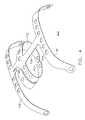
- a portion of the directional antenna array 600is covered with an elastomer 602 as best shown in FIG. 6 .
- the directional antenna array 600can be configured to provide at least a portion of the structural support of the elastomer 602 , and apertures 702 may be formed in one, some, or all of the elements of the directional antenna array 700 as shown in FIG. 7 .
- this low profile and rugged directional antenna arrayis beneficial in numerous electronics applications, including portable or hand-held devices such as cellular telephones, satellite telephones and contactless interrogators of Automatic Identification (Auto ID) systems, such as RFID interrogators of RFID systems.
- Auto IDAutomatic Identification
- the directional antenna array 600includes a near-field antenna 612 that may be used for reading inductively coupled RFID tags (e.g., 125 kHz and 13.56 MHz).
- the near-field antennaincludes conductive current loops ( 604 , 606 ) incorporated with the elastomer 602 and positioned about a parasitic element, such as the director element 104 shown in FIG. 1 .
- the conductive current loops ( 604 , 606 )may also be located in other substrates formed about the parasitic element 104 .
- the conductive current loops ( 604 , 606 )are located in a pair of lobes ( 608 , 610 ) formed by the elastomer 602 and directional antenna array 600 such that each of the conductive current loops ( 604 , 606 ) resides in a corresponding lobe ( 608 , 610 ).
- the lobes ( 608 , 610 )are each located at opposite ends of a longest dimension of the parasitic element, such as a width as illustrated in FIG. 6 .
- the conductive current loops ( 604 , 606 )are positioned to maximize near-field electromagnetic fields while canceling far-field electromagnetic fields.
- the conductive current loops ( 604 , 606 )are constructed to minimize far-field radiated intensity and allow for a stronger near-field pattern. For example, far-field cancellation may be achieved by generating currents of opposite polarity in the conductive current loops ( 604 , 606 ) while maintaining a strong near field.
- a ferrite antenna 614that is effective at lower frequencies such as 13.56 MHz or 135 kHz, such as the ferrite antenna 134 shown in FIG. 1 , may be integrated with the directional antenna array 600 .
- the ferrite antenna 614may be mounted to near the center of the director element, in this exemplary embodiment, between the conductive current loops ( 604 , 606 ).
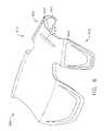
- a portable/handheld device 800is illustrated in accordance with a first exemplary embodiment of the present invention.
- the portable/handheld device 800which in this illustrative example is an RFID interrogator of an RFID system, includes a processing module 804 (e.g., an RFID processing module having any number of configurations known to those of ordinary skill in the art) and the directional antenna array 802 in accordance with one or more of the embodiments of the directional antenna array 802 as previously described in this detailed description.
- a portable/handheld device of other electronic systemscan be formed in accordance with the present invention or non-portable non-handheld devices can be formed in accordance with the present invention.
- the directional antenna array 802has a far-field antenna 816 , such as the Yagi-type previously discussed hereinabove operating at about 915 MHz.
- the directional antenna array 802is configured to include a parasitic element, such as the director element 104 shown in FIG. 1 , having lobes ( 810 , 812 ) similar to the lobes ( 608 , 610 ) shown in FIG. 6 .
- a near-field antenna 814is coupled to the far-field antenna 816 , such as via the elastomer as previously discussed hereinabove.
- the near-field antenna 814includes conductive current loops ( 806 , 808 ), such as the conductive current loops ( 604 , 606 ) shown in FIG. 6 , that are located about the perimeters of the lobes ( 810 , 812 ).
- the conductive current loops ( 806 , 808 )resonate at about 125 kHz and about 13.56 MHz, or other desired frequency bands, for reading inductively coupled tags at the corresponding frequency.
- Additional antenna elementsmay be added to the directional antenna array 802 such as far-field antenna elements. For example, a 2.45 GHz and a 5.6 GHz folded dipole may be co-located on the same substrate as the 915 MHz far-field antenna.
- frequencies bandsmay be used for identification based on a designated frequency for a particular RFID tag.
- antenna elements of the directional antenna arrayare described in the context of folded dipole elements, other types of radiating elements may be used including, but not limited to, slot antenna type elements, non-folded dipole elements, printed circuit patch antenna elements, monopole antenna elements, and the like.
- a ferrite antenna 818such as the ferrite antenna 134 shown in FIG. 1 , is mounted to the near field antenna 814 in a central region between the conductive current loops ( 806 , 808 ).
- the ferrite antenna 818may be fed by a coaxial cable (not shown) that is routed along the boom 108 ( FIG. 1 ) of the directional antenna array 802 .
- a cross-over networkmay be installed with the ferrite antenna 818 such that a single coaxial cable can feed the directional antenna array 802 such that one output of the cross-over network feeds the Yagi antenna (e.g., at about 915 MHz) and another output of the cross-over network feeds the ferrite antenna (e.g., at about 13.56 MHz or about 135 KHz).
- the conductive current loops ( 604 , 606 )are coupled to a current or voltage source (not shown), or the previously discussed electromagnetic field source, that may be housed in the portable/handheld device 800 .
- a current or voltage sourcenot shown
- the conductive current loopsmay be designed based upon a maximum B-field. From the Biot-Savart Law of magnetic induction, conductive current loops or coils with the following ampere-turns produces the desired maximum field strength at a center of the loops:
- N2 ⁇ a t ⁇ B ⁇ 0 Eq . ⁇ 1
- Iis the current
- a tis the radius of the loops
- Bis the magnetic field strength
- ⁇ 0is the magnetic permeability of space.
- the voltage sourcemay be a fixed voltage drive or a constant current drive.
- a series resonant RLC circuitmay be used for a transmitter network having resistance R t , inductance L t , and capacitance C t .
- the fixed voltage driveis generally efficient at delivering maximum current at a resonant frequency and suppressed spurious harmonics outside of the operational frequency band.
- the transmitting networkis adaptively adjustable to the resonant frequency of a receiving network, such as an RFID tag.
- a series RLC circuitis also used for a transmitter network, as previously discussed hereinabove regarding the fixed voltage drive embodiment.
- the constant current drivegenerally maintains constant resultant field strength in spite of induced back-electromagnetic field (EMF) effects that tend to counteract field generation.
- EMFinduced back-electromagnetic field
- the processor module 804determines a specific frequency band associated with an individual RFID tag.
- the processor module 804may control EM emission from each of the near-field antenna 814 , far-field antenna, and additional antenna elements if included in a particular configuration to determine the frequency band for an RFID tag.
- the processor module 804may operate one or more of the near-field antenna elements and far-field antenna elements to poll each of the frequency bands (e.g., 125 kHz, 13.56 MHz, 915 MHz, 2.45 GHz, and 5.6 GHz) for a response from the RFID tag or detection thereof. Once a response is detected from the RFID tag, the processor module 804 tunes the portable/handheld device 800 to the appropriate frequency band.
- the frequency bandse.g., 125 kHz, 13.56 MHz, 915 MHz, 2.45 GHz, and 5.6 GHz
- tuning of the transmitting network coupled to the conductive current loops ( 604 , 606 ) to match the resonant frequency of the conductive current loops ( 604 , 606 ) with an individual RFID tagmay be accomplished using a veractor or similar voltage or current controlled capacitor element placed in parallel with the series resonant capacitor C t .
- a combination of a tunable capacitor for fine tuning and a network of high-quality capacitors for coarse tuningmay also be utilized.
- the processor module 804sets a new resonant frequency by changing both a driving frequency and a total capacitance of the series RLC circuit including any capacitance coupled thereto such as the veractor.
- the processor module 804can determine a proper veractor setting (i.e., capacitance) for series resonance of the changing frequency and when the transmitter and receiver circuits are maximally coupled.
- the processor module 804may also regulate the current into the conductive current loops ( 604 , 606 ) for maintaining desirable field strengths.
- the processor module 804may be coupled to a user input device (not shown), such as a selector switch, that permits a user to select one or more frequency bands for operation. For example, the user may select the 125 kHz and 915 MHz frequency bands for operation of the portable/handheld device 800 .
- the processor module 804controls EM emission from one or more of the near-field antenna 814 , far-field antenna, and additional antenna elements, if included, to poll each of the 125 kHz band and the 915 MHz band for a response from an RFID tag. Any variety of combinations of the aforementioned frequency bands as well as other frequency bands may be selected by the user.
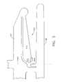
- FIG. 9is a directional antenna array 850 with an elastomer cover 852 in accordance with a second exemplary embodiment of the present invention.
- a portion of the directional antenna array 850and more preferably a substantial portion or substantially all or all of the directional antenna array 850 , is covered with the elastomer 852 .
- the directional antenna array 850can be configured to provide at least a portion of the structural support of the elastomer 852 .
- the directional antenna array 850includes a near-field antenna 854 that may be used for reading inductively coupled RFID tags (e.g., 125 kHz and 13.56 MHz).
- the near-field antenna 854includes a conductive current loop 856 incorporated with the elastomer 852 and positioned about a parasitic element, such as the director element 104 shown in FIG. 1 .
- the conductive current loop 856may also be located in other substrates formed about the parasitic element 104 .
- the conductive current loop 856is located about a perimeter of the director element and encircles a longest dimension of the director element, such as a width as illustrated in FIG. 9 .
- the conductive current loop 856is positioned to generate a stronger near-field electromagnetic fields.
- a slotted antenna 820that is responsive to 2.45 GHz or 5.6 GHz is formed in the directional antenna array 850 .
- a longitudinal slot 820may be formed in a region of the boom and fed by one or more separate coaxial cables (not shown) routed along the boom or the other antenna elements. This is then coupled with a cross-over network (not shown) or fed separately with one or more coaxial cables, as previously discussed hereinabove.
- FIG. 10is a portable/handheld device having the directional antenna array of FIG. 9 in accordance with a second exemplary embodiment of the present invention.
- the portable/handheld device 860is similar to the portable/handheld device 800 shown in FIG. 8 and is also an RFID interrogator of an RFID system having the processing module 862 and the directional antenna array 864 .
- the directional antenna array 864has a far-field antenna 866 , such as the Yagi-type previously discussed hereinabove operating at about 915 MHz.
- the directional antenna array 864is configured to include a parasitic element, such as the director element 104 shown in FIG. 1 .
- a near-field antenna 868is coupled to the far-field antenna 866 , such as via the elastomer as previously discussed hereinabove.
- the near-field antenna 868includes a conductive current loop 870 , such as the conductive current loop 856 shown in FIG. 6 , that is located about the perimeter of the director element 104 .
- the conductive current loop 870may also resonate at about 125 kHz and about 13.56 MHz, or other desired frequency bands, for reading inductively coupled tags at the corresponding frequency.
- Additional antenna elementsmay be added to the directional antenna array 864 , such as far-field antenna elements, as previously mentioned hereinabove.
- a slotted antenna 822such as the slotted antenna 820 shown in FIG. 9 , is formed in the directional antenna array 864 .
- the slotted antenna 820may be configured to be responsive to 2.45 GHz or 5.6 GHz based on the length of the slotted antenna 820 .
- multiple radiating elementssuch as an array, dedicated to respond to 2.45 GHz and 5.6 GHz may be installed with the directional antenna array.
- Such an array of radiating elementsmay be configured to be parasitically-driven, partially all-driven, mostly all-driven, or all-driven on each of the 2.45 GHz and 5.6 GHz frequencies, or on multiple sets of such frequencies.
- This exemplary embodimentmay provide increases in antenna gain by way of increased directivity, effective radiated power (ERP), and corresponding RFID tag read range.
- ERPeffective radiated power
- multiple radiating elementsmay be configured to be electronically steerable.
- the processing module 862is configured to steer a radiated beam from the multiple radiating elements such that ERP may be maximized in desirable directions and minimized in non-desirable directions.
- the radiated beammay be steered away from adjacent interrogators by the processing module 862 so as to minimize interference between the interrogators. This feature is particularly useful in large distribution centers where many docking portals have simultaneously operating interrogators.
- Examples of other arrays of radiating elementsinclude, but are not limited to, an array of different-sized slots that may be used for multiple frequencies of operation and an array of similarly-sized slots that may be collectively used for increased directivity.
- FIG. 11is a flow diagram of a method of reading inductively coupled RFID tags in accordance with an exemplary embodiment of the present invention.
- the methodbegins at step 100 .
- the processing module 804( FIG. 8 ) scans at least one frequency band to detect an RFID tag at step 105 .
- the processing module 804determines a proper veractor setting (i.e., capacitance) for series resonance of the changing frequency and when the transmitter and receiver circuits (e.g., RFID tags) are maximally coupled.
- the processor module 804 ( FIG. 8 )scans for a frequency band selected from the previously mentioned near-field and far-field EM fields including, but not limited to, 915 MHz, 125 kHz, 13.56 MHz, 2.45 GHz, and 5.6 GHz.
- the processor module 804operates one or more of the near-field and far-field antenna elements to selectively radiate an EM field of at least one of the near-field EM field and the far-field EM field based on the detected RFID tag at step 110 .
- the processor module 804may operate a 915 MHz far-field antenna element, such as the far-field antenna 816 shown in FIG. 8 , and a 125 kHz near-field antenna element, such as the near-field antenna 814 shown in FIG. 8 .
- the near-field elementsuch as the near-field antenna 814 having the conductive current loops 806 , 808 shown in FIG. 8 , may be operated to maximize near-field EM radiation that achieves far-field cancellation or minimizes far-field EM radiation from the far-field element, such as the far-field antenna 816 shown in FIG. 8 .
Landscapes
- Engineering & Computer Science (AREA)
- Artificial Intelligence (AREA)
- Computer Vision & Pattern Recognition (AREA)
- Physics & Mathematics (AREA)
- General Physics & Mathematics (AREA)
- Theoretical Computer Science (AREA)
- Aerials With Secondary Devices (AREA)
- Variable-Direction Aerials And Aerial Arrays (AREA)
Abstract
Description
| TABLE 1 | ||||
| Driven | Director | Reflector | ||
| Width | 0.56 inches | 0.49 inches | 0.33 inches | ||
| % Width | 4.35% | 3.8% | 2.57% | ||
| Spacing | Not Applicable | 1.86 inches | 0.89 inches | ||
| % Spacing | Not applicable | 14.4% | 6.9% | ||
| Length | 5.19 inches | 5.04 inches | 5.60 inches | ||
| % Length | 40.2% | 39% inches | 43.4% | ||
Where % Width, % Spacing and % Length are percentages of the free space wavelength and director spacing is the spacing (Sdir1)112 between the driven
where N is the number of turns of loops, I is the current, atis the radius of the loops, B is the magnetic field strength, and μ0is the magnetic permeability of space.
Claims (30)
Priority Applications (6)
| Application Number | Priority Date | Filing Date | Title |
|---|---|---|---|
| US10/957,529US7423606B2 (en) | 2004-09-30 | 2004-09-30 | Multi-frequency RFID apparatus and methods of reading RFID tags |
| CA002581585ACA2581585A1 (en) | 2004-09-30 | 2005-09-22 | Multi-frequency rfid apparatus and methods of reading rfid tags |
| AU2005292331AAU2005292331A1 (en) | 2004-09-30 | 2005-09-22 | Multi-frequency RFID apparatus and methods of reading RFID tags |
| JP2007534684AJP2008515102A (en) | 2004-09-30 | 2005-09-22 | Multi-frequency RFID device and RFID tag reading method |
| PCT/US2005/034356WO2006039229A1 (en) | 2004-09-30 | 2005-09-22 | Multi-frequency rfid apparatus and methods of reading rfid tags |
| EP05813850AEP1794700A1 (en) | 2004-09-30 | 2005-09-22 | Multi-frequency rfid apparatus and methods of reading rfid tags |
Applications Claiming Priority (1)
| Application Number | Priority Date | Filing Date | Title |
|---|---|---|---|
| US10/957,529US7423606B2 (en) | 2004-09-30 | 2004-09-30 | Multi-frequency RFID apparatus and methods of reading RFID tags |
Publications (2)
| Publication Number | Publication Date |
|---|---|
| US20060066441A1 US20060066441A1 (en) | 2006-03-30 |
| US7423606B2true US7423606B2 (en) | 2008-09-09 |
Family
ID=35561467
Family Applications (1)
| Application Number | Title | Priority Date | Filing Date |
|---|---|---|---|
| US10/957,529Active2025-12-13US7423606B2 (en) | 2004-09-30 | 2004-09-30 | Multi-frequency RFID apparatus and methods of reading RFID tags |
Country Status (6)
| Country | Link |
|---|---|
| US (1) | US7423606B2 (en) |
| EP (1) | EP1794700A1 (en) |
| JP (1) | JP2008515102A (en) |
| AU (1) | AU2005292331A1 (en) |
| CA (1) | CA2581585A1 (en) |
| WO (1) | WO2006039229A1 (en) |
Cited By (21)
| Publication number | Priority date | Publication date | Assignee | Title |
|---|---|---|---|---|
| US20070222609A1 (en)* | 2006-03-22 | 2007-09-27 | Symbol Technologies, Inc. | Single frequency low power RFID device |
| US20090073070A1 (en)* | 2007-03-30 | 2009-03-19 | Broadcom Corporation | Dual band antenna and methods for use therewith |
| US20090174557A1 (en)* | 2008-01-03 | 2009-07-09 | Intermec Ip Corp. | Compact flexible high gain antenna for handheld rfid reader |
| US7579995B1 (en)* | 2007-07-30 | 2009-08-25 | Lockheed Martin Corporation | Near field nulling antenna systems |
| USD612369S1 (en)* | 2009-05-13 | 2010-03-23 | Winegard Company | Television antenna |
| US20100117925A1 (en)* | 2008-11-12 | 2010-05-13 | Winegard Company | Mobile television antenna with integrated uhf digital booster |
| US20100117911A1 (en)* | 2008-11-12 | 2010-05-13 | Winegard Company | Uhf digital booster kit for a television antenna and method |
| USD620483S1 (en) | 2009-09-15 | 2010-07-27 | Winegard Company | Television antenna |
| USD624060S1 (en)* | 2010-04-12 | 2010-09-21 | Pds Electronics, Inc. | Antenna feed line |
| US20100302117A1 (en)* | 2009-06-01 | 2010-12-02 | Karin Anne Johnson | Balanced microstrip folded dipole antennas and matching networks |
| US20110133901A1 (en)* | 2009-12-08 | 2011-06-09 | Martin Strzelczyk | Method and device for reading radio frequency identification (rfid) tags |
| US20150035651A1 (en)* | 2013-08-05 | 2015-02-05 | Toshiba Tec Kabushiki Kaisha | Wireless tag communication device and wireless tag communication program |
| US20150101239A1 (en)* | 2012-02-17 | 2015-04-16 | Nathaniel L. Cohen | Apparatus for using microwave energy for insect and pest control and methods thereof |
| US9325080B2 (en) | 2014-03-03 | 2016-04-26 | Apple Inc. | Electronic device with shared antenna structures and balun |
| US9621230B2 (en) | 2014-03-03 | 2017-04-11 | Apple Inc. | Electronic device with near-field antennas |
| US9793616B2 (en) | 2012-11-19 | 2017-10-17 | Apple Inc. | Shared antenna structures for near-field communications and non-near-field communications circuitry |
| US9806422B2 (en) | 2013-09-11 | 2017-10-31 | International Business Machines Corporation | Antenna-in-package structures with broadside and end-fire radiations |
| US9819098B2 (en) | 2013-09-11 | 2017-11-14 | International Business Machines Corporation | Antenna-in-package structures with broadside and end-fire radiations |
| US10312593B2 (en) | 2014-04-16 | 2019-06-04 | Apple Inc. | Antennas for near-field and non-near-field communications |
| USD863268S1 (en) | 2018-05-04 | 2019-10-15 | Scott R. Archer | Yagi-uda antenna with triangle loop |
| USD930628S1 (en)* | 2019-11-25 | 2021-09-14 | Tron Future Tech Inc. | Radar antenna |
Families Citing this family (40)
| Publication number | Priority date | Publication date | Assignee | Title |
|---|---|---|---|---|
| WO2005086802A2 (en) | 2004-03-08 | 2005-09-22 | Proxense, Llc | Linked account system using personal digital key (pdk-las) |
| US7423606B2 (en) | 2004-09-30 | 2008-09-09 | Symbol Technologies, Inc. | Multi-frequency RFID apparatus and methods of reading RFID tags |
| JP4399007B2 (en)* | 2004-11-02 | 2010-01-13 | センサーマティック・エレクトロニクス・コーポレーション | RFID near field microstrip antenna |
| US20110221566A1 (en)* | 2005-02-04 | 2011-09-15 | Douglas Kozlay | Authenticating device with wireless directional radiation |
| JP4407617B2 (en)* | 2005-10-20 | 2010-02-03 | 株式会社デンソー | Wireless communication system |
| KR100743088B1 (en) | 2005-12-29 | 2007-07-27 | 주식회사 팬택 | Apparatus and method for determining radiation pattern and transmit power by measuring received power in RFID reader |
| US11206664B2 (en)* | 2006-01-06 | 2021-12-21 | Proxense, Llc | Wireless network synchronization of cells and client devices on a network |
| US7904718B2 (en) | 2006-05-05 | 2011-03-08 | Proxense, Llc | Personal digital key differentiation for secure transactions |
| US7286097B1 (en)* | 2006-06-08 | 2007-10-23 | Wilson Electronics, Inc. | Yagi antenna with balancing tab |
| WO2008016327A1 (en)* | 2006-08-01 | 2008-02-07 | Agency For Science, Technology And Research | Antenna for near field and far field radio frequency identification |
| US9269221B2 (en) | 2006-11-13 | 2016-02-23 | John J. Gobbi | Configuration of interfaces for a location detection system and application |
| US7997495B2 (en)* | 2007-03-15 | 2011-08-16 | James Neil Rodgers | Precisely tuned RFID antenna |
| US20080238621A1 (en)* | 2007-03-30 | 2008-10-02 | Broadcom Corporation | Multi-mode rfid reader architecture |
| US20090009295A1 (en)* | 2007-03-30 | 2009-01-08 | Broadcom Corporation | Transceiver with far field and near field operation and methods for use therewith |
| US7679514B2 (en) | 2007-03-30 | 2010-03-16 | Broadcom Corporation | Multi-mode RFID tag architecture |
| US8870478B2 (en)* | 2007-05-30 | 2014-10-28 | Zih Corp. | Media processing system and associated spindle |
| US9524460B2 (en)* | 2007-05-30 | 2016-12-20 | Zih Corp. | System for processing media units and an associated media roll |
| EP1998468A3 (en)* | 2007-05-31 | 2012-06-06 | Broadcom Corporation | Multi-mode RFID reader Architecture |
| WO2009011599A1 (en)* | 2007-07-18 | 2009-01-22 | Times-7 Holdings Limited | An rfid tag |
| EP3002820B1 (en)* | 2007-08-02 | 2020-06-03 | University of Pittsburgh - Of the Commonwealth System of Higher Education | Wireless systems having multiple electronic devices and employing simplified fabrication and matching, and associated methods |
| US7830322B1 (en) | 2007-09-24 | 2010-11-09 | Impinj, Inc. | RFID reader antenna assembly |
| US8659427B2 (en) | 2007-11-09 | 2014-02-25 | Proxense, Llc | Proximity-sensor supporting multiple application services |
| US8314706B2 (en)* | 2007-11-16 | 2012-11-20 | Rcd Technology Corporation | Coupled radio frequency identification (RFID) and biometric device |
| US7859415B2 (en)* | 2007-11-16 | 2010-12-28 | Rcd Technology Inc. | RFID based identification device |
| US9415611B2 (en)* | 2007-12-19 | 2016-08-16 | Zih Corp. | Platen incorporating an RFID coupling device |
| WO2009102979A2 (en) | 2008-02-14 | 2009-08-20 | Proxense, Llc | Proximity-based healthcare management system with automatic access to private information |
| US20090295541A1 (en)* | 2008-05-27 | 2009-12-03 | Intellidot Corporation | Directional rfid reader |
| US11476566B2 (en) | 2009-03-09 | 2022-10-18 | Nucurrent, Inc. | Multi-layer-multi-turn structure for high efficiency wireless communication |
| US9342716B2 (en) | 2010-02-04 | 2016-05-17 | Carefusion 303, Inc. | Software-defined multi-mode RFID read devices |
| US9418205B2 (en) | 2010-03-15 | 2016-08-16 | Proxense, Llc | Proximity-based system for automatic application or data access and item tracking |
| CN102918550B (en) | 2010-05-17 | 2016-08-10 | Zih公司 | Double response device RF identification |
| EP2423847B1 (en)* | 2010-08-27 | 2013-03-27 | Psion Inc. | System and method for multiple reading interface with a simple RFID antenna |
| US8857716B1 (en) | 2011-02-21 | 2014-10-14 | Proxense, Llc | Implementation of a proximity-based system for object tracking and automatic application initialization |
| DE102012106594A1 (en)* | 2012-07-20 | 2014-01-23 | J.H. Tönnjes E.A.S.T. GmbH & Co. KG | Vehicle identification means |
| WO2014183106A2 (en) | 2013-05-10 | 2014-11-13 | Proxense, Llc | Secure element as a digital pocket |
| US10438110B2 (en)* | 2015-07-08 | 2019-10-08 | Assa Abloy Ab | Multiple frequency transponder with a single antenna |
| GB201611532D0 (en)* | 2016-07-01 | 2016-08-17 | Dukosi Ltd | Electric batteries |
| US10395071B2 (en) | 2016-12-01 | 2019-08-27 | Avery Dennison Retail Information Services, Llc | Control of RFID reader emissions which may cause interference with systems using RFID tags |
| US11289195B2 (en)* | 2020-08-09 | 2022-03-29 | Kevin Patel | System for remote medical care |
| CN120016148B (en)* | 2025-04-16 | 2025-06-24 | 佛山市健博通电讯实业有限公司 | Ultra-wideband monopole omnidirectional antenna |
Citations (40)
| Publication number | Priority date | Publication date | Assignee | Title |
|---|---|---|---|---|
| US4028709A (en) | 1975-09-10 | 1977-06-07 | The United States Of America As Represented By The Field Operations Bureau Of The Federal Communications Commission | Adjustable yagi antenna |
| US4218686A (en) | 1978-02-23 | 1980-08-19 | Blonder-Tongue Laboratories, Inc. | Yagi-type antennas and method |
| US4336543A (en) | 1977-05-18 | 1982-06-22 | Grumman Corporation | Electronically scanned aircraft antenna system having a linear array of yagi elements |
| US4373163A (en)* | 1980-07-14 | 1983-02-08 | I.D. Engineering, Inc. | Loop antenna for security systems |
| US4700197A (en) | 1984-07-02 | 1987-10-13 | Canadian Patents & Development Ltd. | Adaptive array antenna |
| US5061941A (en)* | 1990-02-01 | 1991-10-29 | Checkpoint Systems, Inc. | Composite antenna for electronic article surveillance systems |
| US5220335A (en) | 1990-03-30 | 1993-06-15 | The United States Of America As Represented By The Administrator Of The National Aeronautics And Space Administration | Planar microstrip Yagi antenna array |
| EP0598624A1 (en) | 1992-11-18 | 1994-05-25 | Btg International Limited | Detection of multiple articles |
| US5493704A (en) | 1992-12-17 | 1996-02-20 | Alcatel N.V. | Portable communications transmitter |
| EP0718912A1 (en) | 1994-12-23 | 1996-06-26 | Alcatel SEL Aktiengesellschaft | Antenna |
| US5612706A (en) | 1994-04-29 | 1997-03-18 | Pacific Monolithics, Inc. | Dual-array yagi antenna |
| USD385563S (en) | 1996-01-11 | 1997-10-28 | Pacific Monolithics, Inc. | Dual-array yagi antenna |
| US5712643A (en) | 1995-12-05 | 1998-01-27 | Cushcraft Corporation | Planar microstrip Yagi Antenna array |
| JPH1032418A (en) | 1996-07-18 | 1998-02-03 | Dx Antenna Co Ltd | Flat antenna |
| US5748156A (en) | 1994-02-28 | 1998-05-05 | Chaparral Communications | High-performance antenna structure |
| WO1998037596A1 (en) | 1997-02-21 | 1998-08-27 | Lusignan Bruce B | Two-way communication system utilizing small c-band antenna for downlink and l-band for uplink |
| US5877728A (en)* | 1997-05-28 | 1999-03-02 | Checkpoint Systems, Inc. | Multiple loop antenna |
| US5898410A (en) | 1997-04-28 | 1999-04-27 | Allen Telecom Inc. | Pre-tuned hybrid logarithmic yagi antenna system |
| US5914692A (en)* | 1997-01-14 | 1999-06-22 | Checkpoint Systems, Inc. | Multiple loop antenna with crossover element having a pair of spaced, parallel conductors for electrically connecting the multiple loops |
| US6061036A (en) | 1998-02-03 | 2000-05-09 | Ericsson, Inc. | Rigid and flexible antenna |
| US6069564A (en) | 1998-09-08 | 2000-05-30 | Hatano; Richard | Multi-directional RFID antenna |
| US6127928A (en) | 1998-02-10 | 2000-10-03 | E-Tag Systems, Inc. | Method and apparatus for locating and tracking documents and other objects |
| JP2000322545A (en) | 1999-05-14 | 2000-11-24 | Toenec Corp | Non-contact type information storage medium |
| JP2001109853A (en) | 1999-10-07 | 2001-04-20 | Toshiba Corp | Portable wireless information processing device |
| US6229491B1 (en) | 1992-08-31 | 2001-05-08 | Northrop Grumman Corporation | Compact Yagi antenna array for aircraft |
| US6307524B1 (en) | 2000-01-18 | 2001-10-23 | Core Technology, Inc. | Yagi antenna having matching coaxial cable and driven element impedances |
| US6326922B1 (en) | 2000-06-29 | 2001-12-04 | Worldspace Corporation | Yagi antenna coupled with a low noise amplifier on the same printed circuit board |
| US6353406B1 (en) | 1996-10-17 | 2002-03-05 | R.F. Technologies, Inc. | Dual mode tracking system |
| EP1209615A2 (en) | 2000-11-06 | 2002-05-29 | Advanced Microwave Engineering di Salvador Claudio e C. S.a.s. | Dual band transponder system |
| US20020105473A1 (en) | 2000-12-07 | 2002-08-08 | Cox Roger A. | One-piece Yagi-Uda antenna and process for making the same |
| US6445297B1 (en) | 2000-10-10 | 2002-09-03 | Escort Memory Systems | Modular RFID antenna system |
| US20020139822A1 (en) | 2001-04-02 | 2002-10-03 | Infanti James C. | Holster apparatus and method for use with a handheld device |
| US20030125725A1 (en) | 2002-01-03 | 2003-07-03 | Afx Inc. | Catheter having improved steering |
| US20030160730A1 (en) | 2002-02-26 | 2003-08-28 | Alsliety Mazen K. | Microstrip Yagi-Uda antenna |
| US6617962B1 (en) | 2000-01-06 | 2003-09-09 | Samsys Technologies Inc. | System for multi-standard RFID tags |
| WO2004015625A1 (en) | 2002-08-08 | 2004-02-19 | Bnc Ip Switzerland Gmbh | Multi-frequency identification device |
| GB2393076A (en) | 2002-09-12 | 2004-03-17 | Rf Tags Ltd | Radio frequency identification tag which has a ground plane not substantially larger than the area spanned by the patch antenna |
| US6809699B2 (en) | 2003-01-27 | 2004-10-26 | Auden Techno Corp. | Dipole antenna array |
| US6922173B2 (en)* | 2002-02-05 | 2005-07-26 | Theodore R. Anderson | Reconfigurable scanner and RFID system using the scanner |
| WO2006039229A1 (en) | 2004-09-30 | 2006-04-13 | Symbol Technologies, Inc. | Multi-frequency rfid apparatus and methods of reading rfid tags |
Family Cites Families (3)
| Publication number | Priority date | Publication date | Assignee | Title |
|---|---|---|---|---|
| JPH07230560A (en)* | 1994-02-18 | 1995-08-29 | Nippon Signal Co Ltd:The | Non-contact automatic ticket checking machine |
| JP3696477B2 (en)* | 2000-04-06 | 2005-09-21 | 松下電器産業株式会社 | Access system |
| JP2002015288A (en)* | 2000-06-30 | 2002-01-18 | Nippon Avionics Co Ltd | RFID multi-purpose interrogator |
- 2004
- 2004-09-30USUS10/957,529patent/US7423606B2/enactiveActive
- 2005
- 2005-09-22CACA002581585Apatent/CA2581585A1/ennot_activeAbandoned
- 2005-09-22JPJP2007534684Apatent/JP2008515102A/enactivePending
- 2005-09-22EPEP05813850Apatent/EP1794700A1/ennot_activeCeased
- 2005-09-22WOPCT/US2005/034356patent/WO2006039229A1/enactiveApplication Filing
- 2005-09-22AUAU2005292331Apatent/AU2005292331A1/ennot_activeAbandoned
Patent Citations (42)
| Publication number | Priority date | Publication date | Assignee | Title |
|---|---|---|---|---|
| US4028709A (en) | 1975-09-10 | 1977-06-07 | The United States Of America As Represented By The Field Operations Bureau Of The Federal Communications Commission | Adjustable yagi antenna |
| US4336543A (en) | 1977-05-18 | 1982-06-22 | Grumman Corporation | Electronically scanned aircraft antenna system having a linear array of yagi elements |
| US4218686A (en) | 1978-02-23 | 1980-08-19 | Blonder-Tongue Laboratories, Inc. | Yagi-type antennas and method |
| US4373163A (en)* | 1980-07-14 | 1983-02-08 | I.D. Engineering, Inc. | Loop antenna for security systems |
| US4700197A (en) | 1984-07-02 | 1987-10-13 | Canadian Patents & Development Ltd. | Adaptive array antenna |
| US5061941A (en)* | 1990-02-01 | 1991-10-29 | Checkpoint Systems, Inc. | Composite antenna for electronic article surveillance systems |
| US5220335A (en) | 1990-03-30 | 1993-06-15 | The United States Of America As Represented By The Administrator Of The National Aeronautics And Space Administration | Planar microstrip Yagi antenna array |
| US6229491B1 (en) | 1992-08-31 | 2001-05-08 | Northrop Grumman Corporation | Compact Yagi antenna array for aircraft |
| EP0598624A1 (en) | 1992-11-18 | 1994-05-25 | Btg International Limited | Detection of multiple articles |
| US5493704A (en) | 1992-12-17 | 1996-02-20 | Alcatel N.V. | Portable communications transmitter |
| US5748156A (en) | 1994-02-28 | 1998-05-05 | Chaparral Communications | High-performance antenna structure |
| US5612706A (en) | 1994-04-29 | 1997-03-18 | Pacific Monolithics, Inc. | Dual-array yagi antenna |
| EP0718912A1 (en) | 1994-12-23 | 1996-06-26 | Alcatel SEL Aktiengesellschaft | Antenna |
| US5712643A (en) | 1995-12-05 | 1998-01-27 | Cushcraft Corporation | Planar microstrip Yagi Antenna array |
| US5913549A (en) | 1995-12-05 | 1999-06-22 | Cushcraft Corporation | Planar microstrip Yagi antenna array and process for making same |
| USD385563S (en) | 1996-01-11 | 1997-10-28 | Pacific Monolithics, Inc. | Dual-array yagi antenna |
| JPH1032418A (en) | 1996-07-18 | 1998-02-03 | Dx Antenna Co Ltd | Flat antenna |
| US6353406B1 (en) | 1996-10-17 | 2002-03-05 | R.F. Technologies, Inc. | Dual mode tracking system |
| US5914692A (en)* | 1997-01-14 | 1999-06-22 | Checkpoint Systems, Inc. | Multiple loop antenna with crossover element having a pair of spaced, parallel conductors for electrically connecting the multiple loops |
| WO1998037596A1 (en) | 1997-02-21 | 1998-08-27 | Lusignan Bruce B | Two-way communication system utilizing small c-band antenna for downlink and l-band for uplink |
| US5898410A (en) | 1997-04-28 | 1999-04-27 | Allen Telecom Inc. | Pre-tuned hybrid logarithmic yagi antenna system |
| US5877728A (en)* | 1997-05-28 | 1999-03-02 | Checkpoint Systems, Inc. | Multiple loop antenna |
| US6061036A (en) | 1998-02-03 | 2000-05-09 | Ericsson, Inc. | Rigid and flexible antenna |
| US6127928A (en) | 1998-02-10 | 2000-10-03 | E-Tag Systems, Inc. | Method and apparatus for locating and tracking documents and other objects |
| US6069564A (en) | 1998-09-08 | 2000-05-30 | Hatano; Richard | Multi-directional RFID antenna |
| JP2000322545A (en) | 1999-05-14 | 2000-11-24 | Toenec Corp | Non-contact type information storage medium |
| JP2001109853A (en) | 1999-10-07 | 2001-04-20 | Toshiba Corp | Portable wireless information processing device |
| US6617962B1 (en) | 2000-01-06 | 2003-09-09 | Samsys Technologies Inc. | System for multi-standard RFID tags |
| US6307524B1 (en) | 2000-01-18 | 2001-10-23 | Core Technology, Inc. | Yagi antenna having matching coaxial cable and driven element impedances |
| US6326922B1 (en) | 2000-06-29 | 2001-12-04 | Worldspace Corporation | Yagi antenna coupled with a low noise amplifier on the same printed circuit board |
| US6445297B1 (en) | 2000-10-10 | 2002-09-03 | Escort Memory Systems | Modular RFID antenna system |
| EP1209615A2 (en) | 2000-11-06 | 2002-05-29 | Advanced Microwave Engineering di Salvador Claudio e C. S.a.s. | Dual band transponder system |
| US20020105473A1 (en) | 2000-12-07 | 2002-08-08 | Cox Roger A. | One-piece Yagi-Uda antenna and process for making the same |
| US6483476B2 (en) | 2000-12-07 | 2002-11-19 | Telex Communications, Inc. | One-piece Yagi-Uda antenna and process for making the same |
| US20020139822A1 (en) | 2001-04-02 | 2002-10-03 | Infanti James C. | Holster apparatus and method for use with a handheld device |
| US20030125725A1 (en) | 2002-01-03 | 2003-07-03 | Afx Inc. | Catheter having improved steering |
| US6922173B2 (en)* | 2002-02-05 | 2005-07-26 | Theodore R. Anderson | Reconfigurable scanner and RFID system using the scanner |
| US20030160730A1 (en) | 2002-02-26 | 2003-08-28 | Alsliety Mazen K. | Microstrip Yagi-Uda antenna |
| WO2004015625A1 (en) | 2002-08-08 | 2004-02-19 | Bnc Ip Switzerland Gmbh | Multi-frequency identification device |
| GB2393076A (en) | 2002-09-12 | 2004-03-17 | Rf Tags Ltd | Radio frequency identification tag which has a ground plane not substantially larger than the area spanned by the patch antenna |
| US6809699B2 (en) | 2003-01-27 | 2004-10-26 | Auden Techno Corp. | Dipole antenna array |
| WO2006039229A1 (en) | 2004-09-30 | 2006-04-13 | Symbol Technologies, Inc. | Multi-frequency rfid apparatus and methods of reading rfid tags |
Non-Patent Citations (1)
| Title |
|---|
| Deal, William R. et al., A Now Quasi-Yagi Antenna For Planar Active Antenna Arrays, IEEE Transactions on Microwave Theory and Techniques, IEEE Inc., New York, US, vol. 48, No. 6, Jun. 2000 pp. 910-918. |
Cited By (41)
| Publication number | Priority date | Publication date | Assignee | Title |
|---|---|---|---|---|
| US20070222609A1 (en)* | 2006-03-22 | 2007-09-27 | Symbol Technologies, Inc. | Single frequency low power RFID device |
| US20100001842A1 (en)* | 2006-03-22 | 2010-01-07 | Mark Duron | Single frequency low power rfid device |
| US7902984B2 (en) | 2006-03-22 | 2011-03-08 | Symbol Technologies, Inc. | Single frequency low power RFID device |
| US7576657B2 (en)* | 2006-03-22 | 2009-08-18 | Symbol Technologies, Inc. | Single frequency low power RFID device |
| US20090073070A1 (en)* | 2007-03-30 | 2009-03-19 | Broadcom Corporation | Dual band antenna and methods for use therewith |
| US8766801B2 (en)* | 2007-03-30 | 2014-07-01 | Broadcom Corporation | Dual band antenna and methods for use therewith |
| US20130052953A1 (en)* | 2007-03-30 | 2013-02-28 | Broadcom Corporation | Dual band antenna and methods for use therewith |
| US8339258B2 (en)* | 2007-03-30 | 2012-12-25 | Broadcom Corporation | Dual band antenna and methods for use therewith |
| US20120034869A1 (en)* | 2007-03-30 | 2012-02-09 | Broadcom Corporation | Dual band antenna and methods for use therewith |
| US8063769B2 (en)* | 2007-03-30 | 2011-11-22 | Broadcom Corporation | Dual band antenna and methods for use therewith |
| US7579995B1 (en)* | 2007-07-30 | 2009-08-25 | Lockheed Martin Corporation | Near field nulling antenna systems |
| US20090174557A1 (en)* | 2008-01-03 | 2009-07-09 | Intermec Ip Corp. | Compact flexible high gain antenna for handheld rfid reader |
| US20100117911A1 (en)* | 2008-11-12 | 2010-05-13 | Winegard Company | Uhf digital booster kit for a television antenna and method |
| US20100117925A1 (en)* | 2008-11-12 | 2010-05-13 | Winegard Company | Mobile television antenna with integrated uhf digital booster |
| US8242968B2 (en) | 2008-11-12 | 2012-08-14 | Winegard Company | Mobile television antenna with integrated UHF digital booster |
| US8018394B2 (en) | 2008-11-12 | 2011-09-13 | Winegard Company | UHF digital booster kit for a television antenna and method |
| USD612369S1 (en)* | 2009-05-13 | 2010-03-23 | Winegard Company | Television antenna |
| US8102327B2 (en)* | 2009-06-01 | 2012-01-24 | The Nielsen Company (Us), Llc | Balanced microstrip folded dipole antennas and matching networks |
| US20100302117A1 (en)* | 2009-06-01 | 2010-12-02 | Karin Anne Johnson | Balanced microstrip folded dipole antennas and matching networks |
| US8446331B2 (en) | 2009-06-01 | 2013-05-21 | The Nielsen Company (Us), Llc | Balanced microstrip folded dipole antennas and matching networks |
| USD620483S1 (en) | 2009-09-15 | 2010-07-27 | Winegard Company | Television antenna |
| US20110133901A1 (en)* | 2009-12-08 | 2011-06-09 | Martin Strzelczyk | Method and device for reading radio frequency identification (rfid) tags |
| US8416060B2 (en) | 2009-12-08 | 2013-04-09 | Symbol Technologies, Inc. | Method and device for reading radio frequency identification (RFID) tags |
| USD624060S1 (en)* | 2010-04-12 | 2010-09-21 | Pds Electronics, Inc. | Antenna feed line |
| US20170181420A1 (en)* | 2012-02-17 | 2017-06-29 | Nathaniel L. Cohen | Apparatus for using microwave energy for insect and pest control and methods thereof |
| US20150101239A1 (en)* | 2012-02-17 | 2015-04-16 | Nathaniel L. Cohen | Apparatus for using microwave energy for insect and pest control and methods thereof |
| US9629354B2 (en)* | 2012-02-17 | 2017-04-25 | Nathaniel L. Cohen | Apparatus for using microwave energy for insect and pest control and methods thereof |
| US9793616B2 (en) | 2012-11-19 | 2017-10-17 | Apple Inc. | Shared antenna structures for near-field communications and non-near-field communications circuitry |
| US9268980B2 (en)* | 2013-08-05 | 2016-02-23 | Toshiba Tec Kabushiki Kaisha | Wireless tag communication device and wireless tag communication program |
| US20150035651A1 (en)* | 2013-08-05 | 2015-02-05 | Toshiba Tec Kabushiki Kaisha | Wireless tag communication device and wireless tag communication program |
| US10170838B2 (en) | 2013-09-11 | 2019-01-01 | International Business Machines Corporation | Antenna-in-package structures with broadside and end-fire radiations |
| US9806422B2 (en) | 2013-09-11 | 2017-10-31 | International Business Machines Corporation | Antenna-in-package structures with broadside and end-fire radiations |
| US9819098B2 (en) | 2013-09-11 | 2017-11-14 | International Business Machines Corporation | Antenna-in-package structures with broadside and end-fire radiations |
| US9917368B2 (en) | 2013-09-11 | 2018-03-13 | International Business Machines Corporation | Antenna-in-package structures with broadside and end-fire radiations |
| US10431892B2 (en) | 2013-09-11 | 2019-10-01 | International Business Machines Corporation | Antenna-in-package structures with broadside and end-fire radiations |
| US9621230B2 (en) | 2014-03-03 | 2017-04-11 | Apple Inc. | Electronic device with near-field antennas |
| US9997828B2 (en) | 2014-03-03 | 2018-06-12 | Apple Inc. | Electronic device with shared antenna structures and balun |
| US9325080B2 (en) | 2014-03-03 | 2016-04-26 | Apple Inc. | Electronic device with shared antenna structures and balun |
| US10312593B2 (en) | 2014-04-16 | 2019-06-04 | Apple Inc. | Antennas for near-field and non-near-field communications |
| USD863268S1 (en) | 2018-05-04 | 2019-10-15 | Scott R. Archer | Yagi-uda antenna with triangle loop |
| USD930628S1 (en)* | 2019-11-25 | 2021-09-14 | Tron Future Tech Inc. | Radar antenna |
Also Published As
| Publication number | Publication date |
|---|---|
| EP1794700A1 (en) | 2007-06-13 |
| US20060066441A1 (en) | 2006-03-30 |
| AU2005292331A1 (en) | 2006-04-13 |
| JP2008515102A (en) | 2008-05-08 |
| CA2581585A1 (en) | 2006-04-13 |
| WO2006039229A1 (en) | 2006-04-13 |
Similar Documents
| Publication | Publication Date | Title |
|---|---|---|
| US7423606B2 (en) | Multi-frequency RFID apparatus and methods of reading RFID tags | |
| US7205953B2 (en) | Directional antenna array | |
| US7215296B2 (en) | Switched multi-beam antenna | |
| US6646606B2 (en) | Double-action antenna | |
| EP1079463B1 (en) | Asymmetric dipole antenna assembly | |
| US6759990B2 (en) | Compact antenna with circular polarization | |
| KR100952797B1 (en) | Antennas and Contactless Tags | |
| US7002521B2 (en) | Antenna device for radio apparatus | |
| US20070159404A1 (en) | Mobile phone having a directed beam antenna | |
| US20070096991A1 (en) | Methods and apparatus for improving wireless communication by antenna polarization position | |
| US6107967A (en) | Billboard antenna | |
| JPH08195609A (en) | Inverted F antenna with built-in portable radio | |
| US7324052B2 (en) | Antenna for a mobile transmitter and/or receiver device | |
| JP2002299950A (en) | Cylindrical slot antenna and polarization diversity antenna | |
| WO2002039538A2 (en) | Compact antenna with multiple polarizations |
Legal Events
| Date | Code | Title | Description |
|---|---|---|---|
| AS | Assignment | Owner name:SYMBOL TECHNOLOGIES, INC., NEW YORK Free format text:ASSIGNMENT OF ASSIGNORS INTEREST;ASSIGNORS:KNADLE, JR., RICHARD T.;CHARYCH, HAL;DURON, MARK WILLIAM;AND OTHERS;REEL/FRAME:015430/0449;SIGNING DATES FROM 20041118 TO 20041129 | |
| STCF | Information on status: patent grant | Free format text:PATENTED CASE | |
| FPAY | Fee payment | Year of fee payment:4 | |
| AS | Assignment | Owner name:MORGAN STANLEY SENIOR FUNDING, INC. AS THE COLLATERAL AGENT, MARYLAND Free format text:SECURITY AGREEMENT;ASSIGNORS:ZIH CORP.;LASER BAND, LLC;ZEBRA ENTERPRISE SOLUTIONS CORP.;AND OTHERS;REEL/FRAME:034114/0270 Effective date:20141027 Owner name:MORGAN STANLEY SENIOR FUNDING, INC. AS THE COLLATE Free format text:SECURITY AGREEMENT;ASSIGNORS:ZIH CORP.;LASER BAND, LLC;ZEBRA ENTERPRISE SOLUTIONS CORP.;AND OTHERS;REEL/FRAME:034114/0270 Effective date:20141027 | |
| AS | Assignment | Owner name:SYMBOL TECHNOLOGIES, LLC, NEW YORK Free format text:CHANGE OF NAME;ASSIGNOR:SYMBOL TECHNOLOGIES, INC.;REEL/FRAME:036083/0640 Effective date:20150410 | |
| AS | Assignment | Owner name:SYMBOL TECHNOLOGIES, INC., NEW YORK Free format text:RELEASE BY SECURED PARTY;ASSIGNOR:MORGAN STANLEY SENIOR FUNDING, INC.;REEL/FRAME:036371/0738 Effective date:20150721 | |
| FPAY | Fee payment | Year of fee payment:8 | |
| MAFP | Maintenance fee payment | Free format text:PAYMENT OF MAINTENANCE FEE, 12TH YEAR, LARGE ENTITY (ORIGINAL EVENT CODE: M1553); ENTITY STATUS OF PATENT OWNER: LARGE ENTITY Year of fee payment:12 |