US7423304B2 - Optimization of critical dimensions and pitch of patterned features in and above a substrate - Google Patents
Optimization of critical dimensions and pitch of patterned features in and above a substrateDownload PDFInfo
- Publication number
- US7423304B2 US7423304B2US10/728,437US72843703AUS7423304B2US 7423304 B2US7423304 B2US 7423304B2US 72843703 AUS72843703 AUS 72843703AUS 7423304 B2US7423304 B2US 7423304B2
- Authority
- US
- United States
- Prior art keywords
- substrate
- pitch
- semiconductor die
- device level
- memory cells
- Prior art date
- Legal status (The legal status is an assumption and is not a legal conclusion. Google has not performed a legal analysis and makes no representation as to the accuracy of the status listed.)
- Expired - Lifetime, expires
Links
Images


Classifications
- H—ELECTRICITY
- H01—ELECTRIC ELEMENTS
- H01L—SEMICONDUCTOR DEVICES NOT COVERED BY CLASS H10
- H01L23/00—Details of semiconductor or other solid state devices
- H01L23/52—Arrangements for conducting electric current within the device in operation from one component to another, i.e. interconnections, e.g. wires, lead frames
- H01L23/522—Arrangements for conducting electric current within the device in operation from one component to another, i.e. interconnections, e.g. wires, lead frames including external interconnections consisting of a multilayer structure of conductive and insulating layers inseparably formed on the semiconductor body
- H01L23/528—Layout of the interconnection structure
- H—ELECTRICITY
- H10—SEMICONDUCTOR DEVICES; ELECTRIC SOLID-STATE DEVICES NOT OTHERWISE PROVIDED FOR
- H10B—ELECTRONIC MEMORY DEVICES
- H10B99/00—Subject matter not provided for in other groups of this subclass
- H10B99/22—Subject matter not provided for in other groups of this subclass including field-effect components
- H—ELECTRICITY
- H01—ELECTRIC ELEMENTS
- H01L—SEMICONDUCTOR DEVICES NOT COVERED BY CLASS H10
- H01L2924/00—Indexing scheme for arrangements or methods for connecting or disconnecting semiconductor or solid-state bodies as covered by H01L24/00
- H01L2924/0001—Technical content checked by a classifier
- H01L2924/0002—Not covered by any one of groups H01L24/00, H01L24/00 and H01L2224/00
Definitions
- a first aspect of the inventionprovides for a semiconductor die comprising a substrate device level having a substrate pitch; and a first above-substrate device level formed above the substrate device level, the first above-substrate device level having a first above-substrate pitch, wherein the first above-substrate pitch is smaller than the substrate pitch.
- a related aspect of the inventionprovides for a semiconductor die comprising a substrate device level having a substrate pitch; and a first memory level above a substrate having a first memory pitch, wherein the first memory pitch is smaller than the substrate pitch.
- Another aspect of the inventionprovides for a monolithic three dimensional memory array comprising a substrate device level comprising devices formed in a substrate having a first pitch; and a first memory level formed over the substrate device having a second pitch, wherein the second pitch is smaller than the first pitch.
- a preferred embodiment of the inventionprovides for a semiconductor die comprising a first device level formed in a substrate, the first device level having a first pitch; and a first plurality of substantially parallel, substantially coplanar rails formed above the substrate, the first plurality of rails having a second pitch, wherein the first pitch is larger than the second pitch.
- An additional aspect of the inventionprovides for a semiconductor device level comprising a first area comprising a plurality of substantially parallel, substantially coplanar rails, the first plurality of rails having a first pitch; and a second area having a second pitch, wherein the second pitch is larger than the first pitch, wherein photolithographic techniques optimized for forming rails are used to pattern the semiconductor device level.
- a preferred embodiment of the inventionprovides for a semiconductor die comprising a substrate device level having a substrate critical dimension; and a first above-substrate device level formed above the substrate device level, the first above-substrate device level having a first above-substrate critical dimension, wherein the first above-substrate critical dimension is smaller than the substrate critical dimension.
- FIG. 1is a cross-sectional view showing depth of focus with different numerical apertures.
- FIG. 2is a cross-sectional view of a CMOS transistor formed in a substrate.
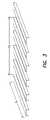
- FIG. 3is a perspective view of substantially parallel, substantially coplanar rails.
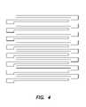
- FIG. 4is a plan view of a portion of a device level having an array area with a first pitch and a second area with a second, larger pitch.
- FIGS. 5 a through 5 dillustrate styles of off-axis illumination which can advantageously be used to pattern very fine features.
- FIGS. 6 a , 6 b , and 6 cillustrate a binary mask, an attenuated phase shift mask, and an alternating phase shift mask.
- FIGS. 7 a , 7 b , and 7 cillustrate the electrical field in the mask plane for a binary mask, an attenuated phase shift mask, and an alternating phase shift mask.
- FIGS. 8 a , 8 b , and 8 cillustrate intensity of light in the wafer plane for a binary mask, an attenuated phase shift mask, and an alternating phase shift mask.
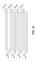
- FIG. 9is a plan view of a wiring arrangement to make electrical connection to a tight memory array.
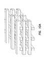
- FIGS. 10 a and 10 bare perspective views of rail and pillar configurations of monolithic three dimensional memories.
- FIG. 11is an elevation view of a semiconductor die including a first device level having a first pitch, a second device level having a second pitch, and a third device level having a third pitch.
- FIG. 12depicts a schematic diagram representing a memory plane within an exemplary three-dimensional passive element memory array.
- FIG. 13is an electrical schematic of a portion of an exemplary memory array.
- semiconductor devicesare formed in a substrate, normally the surface of a semiconductor wafer, most often monocrystalline silicon.
- a substratenormally the surface of a semiconductor wafer, most often monocrystalline silicon.
- transistorsfor example CMOS transistors, in the substrate while forming multiple wiring levels above the substrate.
- Pitchwas defined earlier as the center-to-center distance between features of an integrated circuit. This distance is apparent when features are regular or repeating; for example, when there is a plurality of parallel lines with consistent size and spacing. Pitch can be used to describe features without this regularity as well, however. When features are not regular or repeating, pitch is considered herein to be the sum of the minimum line and the minimum space, even if these features are not next to each other.
- Critical dimensionis the size of the smallest geometrical features (width of interconnect line, contacts, trenches, etc.) which can be formed during semiconductor device/circuit manufacturing using a given technology. Pitch and critical dimension traditionally increase at higher wiring levels for a variety of reasons.
- photoresistis deposited over a surface, then a pattern is projected onto it using a mask.
- the photoresistchanges in response to exposure to light such that the exposed photoresist (or the unexposed photoresist, if negative photoresist is used) is removed in a developing process.
- Finer featurescan be printed by increasing the numerical aperture of the lens used to project the features. For example, turning to FIG. 1 , finer features can be printed using numerical aperture A 1 than numerical aperture A 2 .
- CMPchemical-mechanical polishing
- Monolithic three dimensional memory arraysinvolve extensive fabrication above a semiconductor substrate. Such memory arrays are described in Johnson et al., U.S. Pat. No. 6,034,882, “Vertically Stacked Field Programmable Nonvolatile Memory and Method of Fabrication”; Johnson, U.S. Pat. No. 6,525,953, “Vertically Stacked Field Programmable Nonvolatile Memory and Method of Fabrication”; Knall et al., U.S. Pat. No. 6,420,215, “Three Dimensional Memory Array and Method of Fabrication”; Lee et al., U.S. patent application Ser. No. 09/927,648, “Dense Arrays and Charge Storage Devices, and Methods for Making Same,” filed Aug.
- a monolithic three dimensional memory arrayis one in which multiple memory levels are formed above a single substrate, such as a wafer, with no intervening substrates.
- stacked memorieshave been constructed by forming memory levels on separate substrates and adhering the memory levels atop each other, as in Leedy, U.S. Pat. No. 5,915,167, “Three dimensional structure memory.” The substrates may be thinned or removed from the memory levels before bonding, but as the memory levels are initially formed over separate substrates, such memories are not true monolithic three dimensional memory arrays.
- a plurality of substantially coplanar memory cellsis formed at substantially the same height above a substrate.
- the cellsmay be formed, for example, at the intersections of rails, as in FIG. 10 a , or in pillars interposed between rail intersections, as in FIG. 10 b .
- a plurality of substantially coplanar cells formed at substantially the same height above a substratewill be referred to as a memory level.
- a memory levelis considered to include the rails above and below the memory cell at which they intersect.
- levels immediately adjacentmay share rails, such that the upper rail of one memory level is the lower rail of the one above.
- CMOS support circuitryfor example driver circuitry
- CMOS support circuitryis formed in the substrate, while a plurality of memory levels are formed over the substrate.
- other levelsmay exist, such as wiring or other support circuitry, which may be between the substrate device level and the overlying memory levels, or elsewhere.
- the pitch requirements for the CMOS device level in the substrate and the memory levels above itare largely independent.
- Moving value functionality above the substrateallows the CMOS device level to be formed at lower density, with a larger pitch than the levels above it, reversing the usual trend. It can thus be formed using less expensive lithography tools.
- Use of high-cost lithographycan be limited to memory levels where density is crucial, thus lowering the overall cost of the die.
- a device levelis a plurality of devices formed at substantially the same height in or above a substrate.
- the device levelmay comprise the substrate or may be substantially parallel to the substrate and be formed entirely above it.
- “Substrate”is used herein to refer to a portion of the monocrystalline semiconductor surface, normally a silicon wafer. Traditionally other layers are deposited or grown on this semiconductor surface; these layers are considered to be above the substrate.
- a device level in which any portion of the constituent devices is formed by part of the substrate wafer or located in or below the substrate surfaceis referred to herein as a substrate device level. Vertical interconnects and contacts with the purpose of making electrical contact to a device are not considered to be part of the device.
- An example of a substrate device levelis CMOS transistors formed in the substrate.
- CMOS transistorSuch a CMOS transistor is shown in FIG. 2 .
- the source S, channel region C, and drain D of the transistorare made up of the substrate itself, for example, a monocrystalline silicon wafer.
- the gate electrode Gis formed above the substrate, perhaps of polycrystalline silicon, also called polysilicon. Note that the entire transistor T is considered to be part of a substrate device level, even though part of it, gate electrode G, is formed above the substrate.
- a substrate device levelis a level which has any portion formed in the substrate.
- the present inventionthus provides for a semiconductor die comprising a substrate device level and above-substrate device levels formed above it.
- the substrate device levelhas a substrate critical dimension, while a device level formed above it, for example a memory level, has a smaller critical dimension.
- the substrate critical dimensionis about 0.33 micron, while the above-substrate device level is about 0.25 micron.
- the substrate critical dimensionis about 0.25 micron and the above-substrate critical dimension is about 0.15 micron.
- FIG. 11illustrates a semiconductor die comprising: a substrate device level L 1 having a substrate pitch P 1 ; and a first above-substrate device level L 2 formed above the substrate device level L 1 , the first above-substrate device level having a first above-substrate pitch P 2 , wherein the first above-substrate pitch P 2 is smaller than the substrate pitch P 1 .
- a second above-substrate device level L 3is formed over the first above-substrate device level L 2 , the second above-substrate device level L 3 having a second above-substrate pitch P 3 , wherein the second above-substrate pitch P 3 is smaller than the substrate pitch P 1 .
- intervening layersfor example one or more layers providing electrical interconnection having an intermediate critical dimension or pitch to be formed between the substrate having the substrate critical dimension or pitch and the memory level having the smaller critical dimension or pitch.
- the pitchmay also be larger in the substrate device level than in the above-substrate device level.
- the substrate device level pitchis about 0.65 micron, while the above-substrate device level pitch is about 0.5 micron.
- critical dimensions in the substrate device level and in an above-substrate device levelcan be the same, while pitch is different. This might be the case if, for example, both have features that are 0.15 micron wide, but the intervening space in the substrate device level is larger than the intervening space in the above-substrate device level.
- pitchis the distance from the center of one rail to the center of the rail next to it.
- Critical dimensionis the width of a rail (or of the gap between rails.) If the rails and the gaps between them are the same width, then critical dimension is half of pitch. Critical dimension is always less than pitch, though it may be more than half, less than half, or exactly half of pitch.
- the monolithic three dimensional memory arrays referred to earliercomprise rails such as those shown in FIG. 3 .
- the aim of increasing density of valuable device area while minimizing overall photolithography costcan also be achieved by optimizing lithographic techniques to minimize pitch in the high-value features of a device plane while sacrificing pitch in the lower-value features of the same device plane.
- the uniform, repetitive array area of a memory level in a monolithic three dimensional memory arrayis surrounded by or adjacent to an area providing electrical connections to other memory levels or the substrate; this surrounding or adjacent area will be referred to as the fan-out region.
- the fan-out regiontypically will not have the same repetitive pattern as the features within the array area. An example is shown in FIG. 4 . It may be advantageous to optimize photolithographic techniques to form the dense array area at the expense of the density of the fan-out region.
- Some memory cells in monolithic three dimensional memory arrayscan take the form of diode-antifuse pairs between conductors.
- the antifuseWhen the antifuse is intact, no current flows between the conductors; when the antifuse is ruptured, current is able to flow.
- the state of the antifuse, intact or ruptureddetermines the state of the memory cell, programmed or unprogrammed (or vice versa.)
- the diode-antifuse pairsmay reside in pillars between conductors (as in Johnson or Johnson et al., Herner et al., and Vyvoda et al.), or at the junctions of rails or rail-stacks in a cross-point array (as in Knall et al. and Vyvoda.)
- a memory cellis a field effect transistor with a charge storage region, for example a floating gate or SONOS cell, as in Lee et al., Walker et al., and the '078 application.
- a charge storage regionfor example a floating gate or SONOS cell, as in Lee et al., Walker et al., and the '078 application.
- the presence or absence (or amount) of stored chargedetermines the programmed or unprogrammed state of the memory cell.
- Memory levels of the monolithic three dimensional memory arrays described in the incorporated patents and applicationsare generally laid out in a cross-point array, like those shown in FIG. 10 a or 10 b .
- memory cellsreside at the intersections of rails, as in FIG. 10 a .
- memory cellsreside in pillars disposed between intersecting rails, as in FIG. 10 b .
- Photolithographic techniquescan advantageously be optimized to minimize pitch within the cross-point array.
- substantially parallel linear featuressuch as the conductors in a cross-point array shown in FIG. 3
- this trade-offis advantageous.
- mask biasAnother optimization technique is mask bias. If, for example, it is found that in the regular, uniform part of the array, a critical dimension in the photomask of 0.25 micron will produce an etched feature with a critical dimension of 0.2 micron, and a critical dimension of 0.25 is desired, it may be advantageous to bias the mask; in this case, for example, it may be found that a mask dimension of 0.3 micron will produce an etched dimension of 0.25 micron.
- the regular, repetitive features describedare linear, parallel features. It will be understood by those skilled in the art, however, that other shapes could be repeated in a regular fashion.
- a plurality of pillars that are advantageously arranged uniformlyis patterned and etched. Any repeated pattern, for which photolithographic conditions across a die or across a wafer will be uniform, is highly susceptible to optimization.
- FIG. 5 aWhen patterning using a photomask, light is projected through an illumination aperture.
- Off-axis illuminationin which the illumination aperture is manipulated, can be used to optimize photolithography for patterning regular features.
- the conventional illumination apertureis shown in FIG. 5 a . (These drawings are not to scale.)
- FIG. 5 bAn annular aperture can be used instead, shown in FIG. 5 b .
- the center of the lensis obscured, an annulus around the center admits light, and the outer edge of the lens is obscured.
- measuring from the centerthe center obscured section reaches to between about 0.35 and about 0.6 of the radius. It is preferred for the center obscured section to reach to between about 0.55 and 0.6 of the radius.
- FIG. 5 bshows this section reaching to about 0.55 of the radius.
- the annulus that transmits lightextends from the outer edge of the obscured section, from about 0.35 to about 0.6 of the radius, to a distance from about 0.7 to about 0.875 of the radius; between about 0.8 and about 0.875 of the radius is preferred.
- FIG. 5 bshows the annulus reaching to about 0.8 of the radius. From the transmitting annulus to the outer rim is obscured.
- a quadrupole apertureadmits light through four holes, as shown in FIG. 5 c .
- the outer edge of each holeis between about 0.8 and 0.9 of the radius, preferably at about 0.85 of the radius, while the inner edge of each hole is at about 0.6 to about 0.7 of the radius, preferably at about 0.65 of the radius.
- FIG. 5 cshows the inner edge of each hole at about 0.65 of the radius and the outer edge at about 0.85 of the radius.
- Each holeis circular, and the holes are located with centers rotated 45 degrees from vertical and horizontal, as shown.
- a dipole apertureadmits light through two holes, as shown in FIG. 5 d .
- the outer edge of each holeis between about 0.8 and 0.9 of the radius, preferably at about 0.85 of the radius, while the inner edge of each hole is at about 0.6 to about 0.7 of the radius, preferably at about 0.65 of the radius.
- FIG. 5 dshows the inner edge of each hole at about 0.65 of the radius and the outer edge at about 0.85 of the radius.
- the holesare oriented horizontally and are symmetric about the center point of the lens.
- FIGS. 6 a , 6 b , and 6 cA conventional binary mask, an attenuating phase shift mask, and an alternating phase shift mask are shown in FIGS. 6 a , 6 b , and 6 c , respectively.
- the maskprojects a shape onto photoresist, which is exposed and developed, leaving behind patterned portions of the photoresist which will serve to protect the underlying material from etchants, as is well known in the art.
- the binary masksimply blocks light in some spots and admits it in others.
- the attenuating phase shift mask and the alternating phase shift maskhowever, invert the phase of light as it passes through the mask, causing it to be 180 degrees where the phase is shifted; the electrical field in the mask plane is shown in FIGS. 7 a . 7 b , and 7 c , respectively, for the binary mask, the attenuating phase shift mask, and the alternating phase shift mask.
- the intensity at the surface being patternedis shown in FIGS. 8 a , 8 b , and 8 c , respectively, for the binary mask, the attenuating phase shift mask, and the alternating phase shift mask. It will be seen that the attenuating phase shift mask increases contrast over the binary mask, and the alternating phase shift mask increases it further still.
- An attenuated phase shift maskwill be effective with an annular aperture, better with a quadrupole aperture, and better still with a dipole aperture.
- the dipole apertureis effective for patterning a regular line-space pattern, when the lines being patterned are oriented perpendicular to a line passing between the holes and the center of the lens.
- An alternating phase shift mask paired with a quadrupole apertureis highly effective for patterning regularly spaced pillars.
- a novel alternating phase shift mask useful for patterning regularly spaced pillarsis disclosed in Chen, U.S. patent application Ser. No. 10/728,436, filed on even date herewith and hereby incorporated by reference.
- Photolithographic techniques optimized to form the uniform array arealikely will prove not to be ideal for patterning and etching the less-uniform fan-out region.
- To avoid photolithographic and etching flaws in the fan-out regionit has been found to be advantageous to relax the pitch requirements in the fan-out region so that the fan-out region has a larger pitch, and larger critical dimensions, than the array area.
- the optimizations described here, and othersallow tighter pitch to be achieved in the uniform array area than would normally be achievable given a certain lithography tool.
- a device levelmay comprise two areas.
- the first areacomprises a plurality of substantially parallel, substantially coplanar rails with a first pitch and a first critical dimension.
- the second areacomprises a fan-out region with a second pitch and a second critical dimension.
- the second critical dimensionwill be larger than the first critical dimension. For example, if the first critical dimension is 0.15 micron, the second critical dimension may be 0.3 micron.
- Both array areasare formed in the same patterning steps. Photolithographic techniques optimized for forming rails are used to pattern the semiconductor device level. These techniques likely are not optimal for formation of the fan-out region, but the larger pitch of the fan-out region gives it higher tolerance for error.
- the challengeis compounded as memory levels are stacked atop each other. If, for example, a memory level is formed over a substrate, and three more memory levels are formed over the first memory level, connections must be made to those four levels of conductors, one atop the other, at the end of the array.
- the '887 applicationdescribes a scheme that places the four connections side-by-side at the end of the conductor. This approach successfully places the contacts within pitch, but also increases substrate area used.
- these space-saving via arrangementsinvolve arranging cells in NAND strings, sharing a vertical connection between segmented bit lines to global bit lines, and sharing a vertical connection between segmented word lines all driven by a segmented word line driver.
- the '078 applicationteaches a monolithic three dimensional memory array of thin film transistors having a charge-storage dielectric arranged in series-connected NAND strings.
- Each NAND stringincludes two block select devices for respectively coupling one end of the NAND string to a global bit line and the other end to a shared bias line. Pairs of NAND strings within a block share the same global bit line. NAND strings on more than one layer may be connected to global bit lines on a single layer.
- a preferred embodimentis shown in FIG. 3 of the '078 application.
- FIG. 13an electrical schematic is shown of a portion of an exemplary memory array.
- the portion shownmay represent a two-dimensional array having only one plane of memory cells, or may represent one level of three-dimensional memory array having more than one level (Le., more than one plane) of memory cells.
- a plurality of series-connected NAND transistor stringsis shown, one of which is labeled 122 .
- Each siringincludes a plurality of SONOS transistors connected in series, each gated by a respective one of a plurality of word lines 125 .
- the NAND string 122also includes a block select device 148 for coupling one end of the NAND string to a global bit line contact 131 in accordance with a block select signal BSEL 2 conveyed on node 126 , and further includes a second block select device 147 for coupling the other end of the NAND string to a shared bias node 128 in accordance with a block select signal BSEL 1 conveyed on node 124 .
- the global bit line contact 131is shared with another NAND string 132 which is disposed on the other side of (i.e., opposite) the global bit line contact 131 and is independently selectable by another block select signal BSEL 3 .
- a group of four laterally adjacent NAND stringsshare a common bias node 128 , which may be termed VDRAIN 1 , disposed at the left end of the NAND strings, but are individually coupled to a respective one of four global bit line contacts disposed at the right end of the NAND string.
- VDRAIN 1a common bias node disposed at the left end of the NAND strings
- VDRAIN 2a common bias node disposed at the right end of the NAND strings.
- block select signal BSEL 1couples the left end of half of the NAND strings to an associated global bit line, while the same signal couples the right end of the other half of the NAND strings to the shared bias node VDRAIN 1 .
- block select signal BSEL 2couples the right end of half of the NAND strings to an associated global bit line, while the same signal couples the right end of the other half of the NAND strings to the shared bias node VDRAIN 2 .
- This structureinterleaves the NAND strings by coupling two different NAND strings to the same global bit line.
- the left end of NAND string 134is coupled by BSEL 1 to a global bit line contact 138
- the right end of NAND string 136is coupled by BSEL 2 to a global bit line contact 140 .
- These two global bit line contacts 138 and 140are preferably connected to the same global bit line, which may be routed horizontally on a wire 146 conveyed on a different wiring level.
- Such global bit linesmay be conveyed a wiring level below the array, or alternatively above the array, or alternatively on a wiring level within the array (e.g., in a three-dimensional array having more than one level).
- the NAND string 134 and 136may be referred to as “adjacent” NAND strings, as sharing the same global bit line and sharing the same word lines (i.e., within the same block of the an-ay), even though there is another NAND string disposed between them. It is still possible to select only one of these two NAND strings for reading and writing because the shared bias nodes VRAIN 1 and VDRAIN 2 are distinct and may be driven to different conditions, as is described in regards to the next several figures.
- Each of these two shared bias nodes VDRAIN 1 and VDRAIN 2is shared by NAND strings in two adjacent blocks, and thus arc preferably conveyed in vertical wires 142 and 144 , respectively, which are preferably conveyed on a wiring level “above” the memory array (i.e., further from the semiconductor substrate). Consequently, the two shared bias nodes VDRAIN 1 and VDRAIN 2 , the block select signals BSEL 1 and BSEL 2 , and the various word lines 125 , which all traverse across the memory array in the same direction, may be more conveniently decoded and driven to appropriate levels.
- the memory cells in the NAND stringsare preferably SONOS structures.
- SONOSis meant to refer to the general class of transistor devices having a charge storage dielectric layer between the gate and the underlying channel, and is not used in a restrictive sense to merely imply a literal silicon-oxide-nitride-oxide-silicon layer stack.
- dielectric layersmay be employed, such as oxynitrides, as is described in greater detail herebelow.
- a basic NAND stringis a very efficient structure, capable of achieving a 4F 2 layout for the incremental transistor memory cell.
- the structure depicted in FIG. 13achieves very dense layout because of the interleaving of two NAND strings, both coupled to the same global bit line, thus relaxing the pitch requirements for the global bit lines by a factor of two.
- the structure depicted in FIG. 13also achieves very dense layout because only one control signal is utilized at each end of the NAND strings.
- the block select devicesmay be SONOS devices just like the memory cell devices.
- each memory levelconsequently includes only one type of device, further simplifying the fabrication of each level.
- the block select devicesmay be sized identically to the memory cell devices, but preferably may have a longer channel length (i.e., wider polysilicon stripe for the block select signals) to increase the breakdown voltage of the block select devices.
- the substantially parallel, coplanar railscomprise at least two pluralities of memory lines.
- a first plurality 95 of memory linesis electrically connected to a first plurality 91 of vertical interconnects at a first end and a second plurality 96 of memory lines is electrically connected to a second plurality 92 of vertical interconnects at a second end opposite the first end, and the first and second pluralities of memory lines interleaved.
- Any other relevant techniques from the '078 applicationmay be used as well.
- FIG. 12a schematic diagram is depicted which represents a memory plane within an exemplary three-dimensional passive element memory array.
- the memory plane 150includes a plurality of blocks, such as blocks 151 , 152 , and 153 .
- Each blockincludes a plurality of word lines, such as word lines 156 associated with block 152 .
- Each blockalso includes a plurality of bit line segments, such as bit line segments 157 , 158 , 159 , and 160 associated with block 152 .
- a memory celle.g., memory cell 173
- Each bit line segmentmay be coupled to an associated global bit line by a segment switch device which is controlled by a block select signal.
- bit line segment 157is coupled by a segment switch device 161 to global bit line 154 , which preferably resides on a different layer of the memory array.
- the connection path to the global bit lineis formed by way of a vertical connection 167 , which is shared by other memory planes, to provide a path for a bit line segment from any of at least two memory planes to be coupled to the global bit line.
- bit line segments of memory plane 150are arranged in a 2:1 interleaved configuration, which allows the required pitch of the global bit lines to be twice that of the bit line segments.
- half of the bit line segments within a blockexit to the top of the block and are coupled under control of a SELECT-A control signal to the respective global bit lines, while the other half of the bit line segments exit to the bottom of the block and are coupled under control of a SELECT-B control signal to the same respective global bit lines.
- bit line segment 158is coupled by segment switch device 163 to a shared vertical connection 169 to global bit line 154
- bit line segment 159is coupled by segment switch device 162 to a shared vertical connection 168 to global bit line 155
- bit line segment 160is coupled by segment switch device 164 to a shared vertical connection 170 to global bit line 155 .
- each of the shared vertical connections(which are shared vertically with other memory planes) is also shared by a bit line segment in an adjacent memory block within the same memory plane.
- a bit line segment in block 151(unlabeled) is coupled by segment switch device 171 (under control of a block select signal SELECT-E) to the same shared vertical connection 167 , and consequently to global bit line 154 .
- SELECT-Eblock select signal
- bit line segment in block 151is coupled by segment switch device 172 (controlled by SELECT-E) to the shared vertical connection 168 , and consequently to global bit line 155 .
- segment switch device 172controlled by SELECT-E
- bit line segments from memory block 153are respectively coupled by segment switch devices 165 , 166 to shared vertical connections 169 , 170 and consequently to global bit lines.
- 154 , 155are respectively coupled by segment switch devices 165 , 166 to shared vertical connections 169 , 170 and consequently to global bit lines.
- each global bit lineis operably coupled to a respective bit line segment in a selected block of a selected memory plane by driving one of the two block select control signals associated with the selected block to an active state, while leaving the other block select control signal of the selected block, and all other blocks (both on the same memory plane and on other memory planes sharing the same global bit lines), at an inactive level.
- the signal from a memory cellis coupled from the bit line segment to a global bit line, and subsequently to sensing circuitry.
- the programming voltages and currentsare conveyed from write driver circuitry, through the global bit Line, through the segment switch device to the bit line segment, and coupled thereby to the selected memory cell.
- a shared vertical connectionpreferably connects the word line segments together and connects to a word line driver circuit disposed generally below the array near the word line.
- Each word line driver circuitpreferably couples its word line either to an associated one of a plurality of selected bias lines or to an unselected bias line associated with the driver circuit, which selected bias lines are themselves decoded to provide for an efficient multi-headed word line decoder as shown in FIG. 9 of the '844 application.
- support circuitrylike decoders and drivers, require extensive interconnectivity to the memory array, limiting its practical placement to the area immediately surrounding the memory array.
- Some circuitry formed in the substratedoesn't require connections to conductors within the memory array, and thus can be placed under the memory array.
- Such circuitrymight be a charge pump, for example, or supplemental volatile or nonvolatile memory. If adequate space remains under the array to form these circuits at larger pitch than the memory array, the decrease in fabrication cost is pure economic gain.
- the decision whether or not to relax pitch in a substrate device level relative to an above-substrate device levelis typically based on cost.
- Use of the space-saving arrangements described hereindecrease the substrate area of the memory array and its support circuitry, and thus the overall cost.
Landscapes
- Physics & Mathematics (AREA)
- Geometry (AREA)
- Condensed Matter Physics & Semiconductors (AREA)
- General Physics & Mathematics (AREA)
- Engineering & Computer Science (AREA)
- Computer Hardware Design (AREA)
- Microelectronics & Electronic Packaging (AREA)
- Power Engineering (AREA)
- Semiconductor Memories (AREA)
Abstract
Description
Claims (26)
Priority Applications (3)
| Application Number | Priority Date | Filing Date | Title |
|---|---|---|---|
| US10/728,437US7423304B2 (en) | 2003-12-05 | 2003-12-05 | Optimization of critical dimensions and pitch of patterned features in and above a substrate |
| US12/136,766US8283706B2 (en) | 2003-12-05 | 2008-06-10 | Optimization of critical dimensions and pitch of patterned features in and above a substrate |
| US13/613,956US8766332B2 (en) | 2003-12-05 | 2012-09-13 | Optimization of critical dimensions and pitch of patterned features in and above a substrate |
Applications Claiming Priority (1)
| Application Number | Priority Date | Filing Date | Title |
|---|---|---|---|
| US10/728,437US7423304B2 (en) | 2003-12-05 | 2003-12-05 | Optimization of critical dimensions and pitch of patterned features in and above a substrate |
Related Child Applications (1)
| Application Number | Title | Priority Date | Filing Date |
|---|---|---|---|
| US12/136,766DivisionUS8283706B2 (en) | 2003-12-05 | 2008-06-10 | Optimization of critical dimensions and pitch of patterned features in and above a substrate |
Publications (2)
| Publication Number | Publication Date |
|---|---|
| US20050121790A1 US20050121790A1 (en) | 2005-06-09 |
| US7423304B2true US7423304B2 (en) | 2008-09-09 |
Family
ID=34633712
Family Applications (3)
| Application Number | Title | Priority Date | Filing Date |
|---|---|---|---|
| US10/728,437Expired - LifetimeUS7423304B2 (en) | 2003-12-05 | 2003-12-05 | Optimization of critical dimensions and pitch of patterned features in and above a substrate |
| US12/136,766Expired - Fee RelatedUS8283706B2 (en) | 2003-12-05 | 2008-06-10 | Optimization of critical dimensions and pitch of patterned features in and above a substrate |
| US13/613,956Expired - Fee RelatedUS8766332B2 (en) | 2003-12-05 | 2012-09-13 | Optimization of critical dimensions and pitch of patterned features in and above a substrate |
Family Applications After (2)
| Application Number | Title | Priority Date | Filing Date |
|---|---|---|---|
| US12/136,766Expired - Fee RelatedUS8283706B2 (en) | 2003-12-05 | 2008-06-10 | Optimization of critical dimensions and pitch of patterned features in and above a substrate |
| US13/613,956Expired - Fee RelatedUS8766332B2 (en) | 2003-12-05 | 2012-09-13 | Optimization of critical dimensions and pitch of patterned features in and above a substrate |
Country Status (1)
| Country | Link |
|---|---|
| US (3) | US7423304B2 (en) |
Cited By (25)
| Publication number | Priority date | Publication date | Assignee | Title |
|---|---|---|---|---|
| US20050052915A1 (en)* | 2002-12-19 | 2005-03-10 | Matrix Semiconductor, Inc. | Nonvolatile memory cell without a dielectric antifuse having high- and low-impedance states |
| US20050226067A1 (en)* | 2002-12-19 | 2005-10-13 | Matrix Semiconductor, Inc. | Nonvolatile memory cell operating by increasing order in polycrystalline semiconductor material |
| US20060067117A1 (en)* | 2004-09-29 | 2006-03-30 | Matrix Semiconductor, Inc. | Fuse memory cell comprising a diode, the diode serving as the fuse element |
| US20070069217A1 (en)* | 2003-12-03 | 2007-03-29 | Herner S B | P-i-n diode crystallized adjacent to a silicide in series with a dielectric anitfuse |
| US20070105284A1 (en)* | 2003-12-03 | 2007-05-10 | Herner S B | Method for forming a memory cell comprising a semiconductor junction diode crystallized adjacent to a silicide |
| US20080054372A1 (en)* | 2004-04-04 | 2008-03-06 | Guobiao Zhang | Small-Pitch Three-Dimensional Mask-Programmable Memory |
| US20080310231A1 (en)* | 2003-12-05 | 2008-12-18 | Cleeves James M | Optimization of critical dimensions and pitch of patterned features in and above a substrate |
| US20090142921A1 (en)* | 2005-03-25 | 2009-06-04 | Sandisk 3D Llc | Method for reducing dielectric overetch when making contact to conductive features |
| US20100136751A1 (en)* | 2003-12-03 | 2010-06-03 | Herner S Brad | Method for making a p-i-n diode crystallized adjacent to a silicide in series with a dielectric antifuse |
| US20100181657A1 (en)* | 2002-12-19 | 2010-07-22 | Sandisk 3D Llc | Nonvolatile memory cell comprising a reduced height vertical diode |
| US20100297834A1 (en)* | 2005-03-25 | 2010-11-25 | Dunton Samuel V | Method for reducing dielectric overetch using a dielectric etch stop at a planar surface |
| US8004033B2 (en) | 2002-12-19 | 2011-08-23 | Sandisk 3D Llc | High-density nonvolatile memory |
| US8102698B2 (en) | 2005-01-19 | 2012-01-24 | Sandisk 3D Llc | Structure and method for biasing phase change memory array for reliable writing |
| US9001555B2 (en) | 2012-03-30 | 2015-04-07 | Chengdu Haicun Ip Technology Llc | Small-grain three-dimensional memory |
| US9123393B2 (en) | 2011-09-01 | 2015-09-01 | HangZhou KiCun nformation Technology Co. Ltd. | Discrete three-dimensional vertical memory |
| US9293509B2 (en) | 2013-03-20 | 2016-03-22 | HangZhou HaiCun Information Technology Co., Ltd. | Small-grain three-dimensional memory |
| US9299390B2 (en) | 2011-09-01 | 2016-03-29 | HangZhou HaiCun Informationa Technology Co., Ltd. | Discrete three-dimensional vertical memory comprising off-die voltage generator |
| US9305604B2 (en) | 2011-09-01 | 2016-04-05 | HangZhou HaiCun Information Technology Co., Ltd. | Discrete three-dimensional vertical memory comprising off-die address/data-translator |
| US9305605B2 (en) | 2011-09-01 | 2016-04-05 | Chengdu Haicun Ip Technology Llc | Discrete three-dimensional vertical memory |
| US9396764B2 (en) | 2011-09-01 | 2016-07-19 | HangZhou HaiCun Information Technology Co., Ltd. | Discrete three-dimensional memory |
| US9508395B2 (en) | 2011-09-01 | 2016-11-29 | HangZhou HaiCun Information Technology Co., Ltd. | Three-dimensional one-time-programmable memory comprising off-die read/write-voltage generator |
| US9558842B2 (en) | 2011-09-01 | 2017-01-31 | HangZhou HaiCun Information Technology Co., Ltd. | Discrete three-dimensional one-time-programmable memory |
| US9559082B2 (en) | 2011-09-01 | 2017-01-31 | HangZhou HaiCun Information Technology Co., Ltd. | Three-dimensional vertical memory comprising dice with different interconnect levels |
| US9666300B2 (en) | 2011-09-01 | 2017-05-30 | XiaMen HaiCun IP Technology LLC | Three-dimensional one-time-programmable memory comprising off-die address/data-translator |
| US10763118B2 (en) | 2018-07-11 | 2020-09-01 | International Business Machines Corporation | Cyclic selective deposition for tight pitch patterning |
Families Citing this family (19)
| Publication number | Priority date | Publication date | Assignee | Title |
|---|---|---|---|---|
| US7233522B2 (en)* | 2002-12-31 | 2007-06-19 | Sandisk 3D Llc | NAND memory array incorporating capacitance boosting of channel regions in unselected memory cells and method for operation of same |
| US7505321B2 (en)* | 2002-12-31 | 2009-03-17 | Sandisk 3D Llc | Programmable memory array structure incorporating series-connected transistor strings and methods for fabrication and operation of same |
| US7221588B2 (en)* | 2003-12-05 | 2007-05-22 | Sandisk 3D Llc | Memory array incorporating memory cells arranged in NAND strings |
| US20050128807A1 (en)* | 2003-12-05 | 2005-06-16 | En-Hsing Chen | Nand memory array incorporating multiple series selection devices and method for operation of same |
| US7339272B2 (en)* | 2004-06-14 | 2008-03-04 | Taiwan Semiconductor Manufacturing Company, Ltd. | Semiconductor device with scattering bars adjacent conductive lines |
| US7177191B2 (en)* | 2004-12-30 | 2007-02-13 | Sandisk 3D Llc | Integrated circuit including memory array incorporating multiple types of NAND string structures |
| DE102005003185B4 (en)* | 2005-01-19 | 2006-11-02 | Infineon Technologies Ag | An imaging system and method of fabricating semiconductor structures on a wafer by imaging a mask on the wafer with a dipole aperture |
| DE102005003183B4 (en)* | 2005-01-19 | 2011-06-16 | Qimonda Ag | Process for producing semiconductor structures on a wafer |
| US7359279B2 (en)* | 2005-03-31 | 2008-04-15 | Sandisk 3D Llc | Integrated circuit memory array configuration including decoding compatibility with partial implementation of multiple memory layers |
| US7054219B1 (en) | 2005-03-31 | 2006-05-30 | Matrix Semiconductor, Inc. | Transistor layout configuration for tight-pitched memory array lines |
| US7142471B2 (en)* | 2005-03-31 | 2006-11-28 | Sandisk 3D Llc | Method and apparatus for incorporating block redundancy in a memory array |
| US7272052B2 (en)* | 2005-03-31 | 2007-09-18 | Sandisk 3D Llc | Decoding circuit for non-binary groups of memory line drivers |
| JP5283943B2 (en)* | 2008-03-25 | 2013-09-04 | 株式会社東芝 | Semiconductor device |
| KR20110104767A (en)* | 2010-03-17 | 2011-09-23 | 주식회사 하이닉스반도체 | Method for manufacturing semiconductor device |
| US8466560B2 (en)* | 2010-12-30 | 2013-06-18 | Stmicroelectronics, Inc. | Dummy structures having a golden ratio and method for forming the same |
| EP2693271A1 (en)* | 2012-08-02 | 2014-02-05 | LayTec AG | Apparatus and method for measuring the dimensions of 1-dimensional and 0-dimensional nanostructures in real-time during epitaxial growth |
| US8988917B2 (en)* | 2012-11-15 | 2015-03-24 | Sandisk Technologies Inc. | Bit line resistance compensation |
| US9105636B2 (en) | 2013-08-26 | 2015-08-11 | Micron Technology, Inc. | Semiconductor constructions and methods of forming electrically conductive contacts |
| KR102309566B1 (en)* | 2015-03-20 | 2021-10-07 | 에스케이하이닉스 주식회사 | Semiconductor device |
Citations (12)
| Publication number | Priority date | Publication date | Assignee | Title |
|---|---|---|---|---|
| US4498226A (en)* | 1981-08-31 | 1985-02-12 | Tokyo Shibaura Denki Kabushiki Kaisha | Method for manufacturing three-dimensional semiconductor device by sequential beam epitaxy |
| US5060045A (en)* | 1988-10-17 | 1991-10-22 | Hitachi, Ltd. | Semiconductor integrated circuit device and method of manufacturing the same |
| US5266511A (en)* | 1991-10-02 | 1993-11-30 | Fujitsu Limited | Process for manufacturing three dimensional IC's |
| US5587948A (en)* | 1994-06-17 | 1996-12-24 | Kabushiki Kaisha Toshiba | Nonvolatile semiconductor memory with NAND structure memory arrays |
| US5621683A (en)* | 1994-12-06 | 1997-04-15 | U.S. Philips Corporation | Semiconductor memory with non-volatile memory transistor |
| US6373553B1 (en) | 1999-09-20 | 2002-04-16 | Intel Corp. | Photo-lithographic method to print a line-space pattern with a pitch equal to half the pitch of the mask |
| US6486066B2 (en)* | 2001-02-02 | 2002-11-26 | Matrix Semiconductor, Inc. | Method of generating integrated circuit feature layout for improved chemical mechanical polishing |
| JP3393923B2 (en)* | 1994-06-01 | 2003-04-07 | 三菱電機株式会社 | Semiconductor storage device |
| US6631085B2 (en)* | 2000-04-28 | 2003-10-07 | Matrix Semiconductor, Inc. | Three-dimensional memory array incorporating serial chain diode stack |
| US20030198101A1 (en)* | 2002-02-20 | 2003-10-23 | Stmicroelectronics S.R.L. | Word line selector for a semiconductor memory |
| US20040125629A1 (en)* | 2002-12-31 | 2004-07-01 | Scheuerlein Roy E. | Programmable memory array structure incorporating series-connected transistor strings and methods for fabrication and operation of same |
| US20040188714A1 (en)* | 2003-03-31 | 2004-09-30 | Scheuerlein Roy E. | Three-dimensional memory device incorporating segmented bit line memory array |
Family Cites Families (25)
| Publication number | Priority date | Publication date | Assignee | Title |
|---|---|---|---|---|
| JPH05102430A (en)* | 1991-04-23 | 1993-04-23 | Mitsubishi Electric Corp | Semiconductor device and manufacture thereof |
| US6201521B1 (en)* | 1995-09-29 | 2001-03-13 | Texas Instruments Incorporated | Divided reset for addressing spatial light modulator |
| US5691230A (en)* | 1996-09-04 | 1997-11-25 | Micron Technology, Inc. | Technique for producing small islands of silicon on insulator |
| KR100206709B1 (en)* | 1996-09-21 | 1999-07-01 | 윤종용 | Cell array structure of multi-bit non-volatile semiconductor memory and fabrication method thereof |
| US5770482A (en)* | 1996-10-08 | 1998-06-23 | Advanced Micro Devices, Inc. | Multi-level transistor fabrication method with a patterned upper transistor substrate and interconnection thereto |
| US5915167A (en) | 1997-04-04 | 1999-06-22 | Elm Technology Corporation | Three dimensional structure memory |
| US6153490A (en)* | 1997-07-01 | 2000-11-28 | Texas Instruments Incorporated | Method for forming integrated circuit capacitor and memory |
| US6323081B1 (en)* | 1998-09-03 | 2001-11-27 | Micron Technology, Inc. | Diffusion barrier layers and methods of forming same |
| US6034882A (en) | 1998-11-16 | 2000-03-07 | Matrix Semiconductor, Inc. | Vertically stacked field programmable nonvolatile memory and method of fabrication |
| JP2001044281A (en)* | 1999-07-27 | 2001-02-16 | Mitsubishi Electric Corp | Semiconductor device with multilayer wiring structure |
| US6856572B2 (en) | 2000-04-28 | 2005-02-15 | Matrix Semiconductor, Inc. | Multi-headed decoder structure utilizing memory array line driver with dual purpose driver device |
| US6566698B2 (en)* | 2000-05-26 | 2003-05-20 | Sony Corporation | Ferroelectric-type nonvolatile semiconductor memory and operation method thereof |
| KR100821456B1 (en) | 2000-08-14 | 2008-04-11 | 샌디스크 쓰리디 엘엘씨 | Dense array and charge storage device and manufacturing method thereof |
| US6525953B1 (en) | 2001-08-13 | 2003-02-25 | Matrix Semiconductor, Inc. | Vertically-stacked, field-programmable, nonvolatile memory and method of fabrication |
| US6664173B2 (en)* | 2002-01-09 | 2003-12-16 | Intel Corporation | Hardmask gate patterning technique for all transistors using spacer gate approach for critical dimension control |
| US6940748B2 (en)* | 2002-05-16 | 2005-09-06 | Micron Technology, Inc. | Stacked 1T-nMTJ MRAM structure |
| US6754124B2 (en)* | 2002-06-11 | 2004-06-22 | Micron Technology, Inc. | Hybrid MRAM array structure and operation |
| US6952043B2 (en) | 2002-06-27 | 2005-10-04 | Matrix Semiconductor, Inc. | Electrically isolated pillars in active devices |
| US7005350B2 (en) | 2002-12-31 | 2006-02-28 | Matrix Semiconductor, Inc. | Method for fabricating programmable memory array structures incorporating series-connected transistor strings |
| US6879505B2 (en) | 2003-03-31 | 2005-04-12 | Matrix Semiconductor, Inc. | Word line arrangement having multi-layer word line segments for three-dimensional memory array |
| US7511352B2 (en) | 2003-05-19 | 2009-03-31 | Sandisk 3D Llc | Rail Schottky device and method of making |
| US7153753B2 (en)* | 2003-08-05 | 2006-12-26 | Micron Technology, Inc. | Strained Si/SiGe/SOI islands and processes of making same |
| US7474000B2 (en) | 2003-12-05 | 2009-01-06 | Sandisk 3D Llc | High density contact to relaxed geometry layers |
| US7172840B2 (en) | 2003-12-05 | 2007-02-06 | Sandisk Corporation | Photomask features with interior nonprinting window using alternating phase shifting |
| US7423304B2 (en) | 2003-12-05 | 2008-09-09 | Sandisck 3D Llc | Optimization of critical dimensions and pitch of patterned features in and above a substrate |
- 2003
- 2003-12-05USUS10/728,437patent/US7423304B2/ennot_activeExpired - Lifetime
- 2008
- 2008-06-10USUS12/136,766patent/US8283706B2/ennot_activeExpired - Fee Related
- 2012
- 2012-09-13USUS13/613,956patent/US8766332B2/ennot_activeExpired - Fee Related
Patent Citations (12)
| Publication number | Priority date | Publication date | Assignee | Title |
|---|---|---|---|---|
| US4498226A (en)* | 1981-08-31 | 1985-02-12 | Tokyo Shibaura Denki Kabushiki Kaisha | Method for manufacturing three-dimensional semiconductor device by sequential beam epitaxy |
| US5060045A (en)* | 1988-10-17 | 1991-10-22 | Hitachi, Ltd. | Semiconductor integrated circuit device and method of manufacturing the same |
| US5266511A (en)* | 1991-10-02 | 1993-11-30 | Fujitsu Limited | Process for manufacturing three dimensional IC's |
| JP3393923B2 (en)* | 1994-06-01 | 2003-04-07 | 三菱電機株式会社 | Semiconductor storage device |
| US5587948A (en)* | 1994-06-17 | 1996-12-24 | Kabushiki Kaisha Toshiba | Nonvolatile semiconductor memory with NAND structure memory arrays |
| US5621683A (en)* | 1994-12-06 | 1997-04-15 | U.S. Philips Corporation | Semiconductor memory with non-volatile memory transistor |
| US6373553B1 (en) | 1999-09-20 | 2002-04-16 | Intel Corp. | Photo-lithographic method to print a line-space pattern with a pitch equal to half the pitch of the mask |
| US6631085B2 (en)* | 2000-04-28 | 2003-10-07 | Matrix Semiconductor, Inc. | Three-dimensional memory array incorporating serial chain diode stack |
| US6486066B2 (en)* | 2001-02-02 | 2002-11-26 | Matrix Semiconductor, Inc. | Method of generating integrated circuit feature layout for improved chemical mechanical polishing |
| US20030198101A1 (en)* | 2002-02-20 | 2003-10-23 | Stmicroelectronics S.R.L. | Word line selector for a semiconductor memory |
| US20040125629A1 (en)* | 2002-12-31 | 2004-07-01 | Scheuerlein Roy E. | Programmable memory array structure incorporating series-connected transistor strings and methods for fabrication and operation of same |
| US20040188714A1 (en)* | 2003-03-31 | 2004-09-30 | Scheuerlein Roy E. | Three-dimensional memory device incorporating segmented bit line memory array |
Non-Patent Citations (1)
| Title |
|---|
| S. Wolf et al., Silicon Processing, 2000, Lattice Press, p. 1.* |
Cited By (49)
| Publication number | Priority date | Publication date | Assignee | Title |
|---|---|---|---|---|
| US20110176352A1 (en)* | 2002-12-19 | 2011-07-21 | Herner S Brad | Nonvolatile memory cell operating by increasing order in polycrystalline semiconductor material |
| US8004033B2 (en) | 2002-12-19 | 2011-08-23 | Sandisk 3D Llc | High-density nonvolatile memory |
| US8637366B2 (en) | 2002-12-19 | 2014-01-28 | Sandisk 3D Llc | Nonvolatile memory cell without a dielectric antifuse having high- and low-impedance states |
| US8482973B2 (en) | 2002-12-19 | 2013-07-09 | Sandisk 3D Llc | Nonvolatile memory cell operating by increasing order in polycrystalline semiconductor material |
| US8383478B2 (en) | 2002-12-19 | 2013-02-26 | Sandisk 3D Llc | High-density nonvolatile memory and methods of making the same |
| US8252644B2 (en) | 2002-12-19 | 2012-08-28 | Sandisk 3D Llc | Method for forming a nonvolatile memory cell comprising a reduced height vertical diode |
| US8730720B2 (en) | 2002-12-19 | 2014-05-20 | Sandisk 3D Llc | Nonvolatile memory cell operating by increasing order in polycrystalline semiconductor material |
| US9246089B2 (en) | 2002-12-19 | 2016-01-26 | Sandisk 3D Llc | Nonvolatile memory cell without a dielectric antifuse having high- and low-impedance states |
| US8243509B2 (en) | 2002-12-19 | 2012-08-14 | Sandisk 3D Llc | Nonvolatile memory cell operating by increasing order in polycrystalline semiconductor material |
| US8018025B2 (en) | 2002-12-19 | 2011-09-13 | Sandisk 3D Llc | Nonvolatile memory cell comprising a reduced height vertical diode |
| US20100181657A1 (en)* | 2002-12-19 | 2010-07-22 | Sandisk 3D Llc | Nonvolatile memory cell comprising a reduced height vertical diode |
| US20050226067A1 (en)* | 2002-12-19 | 2005-10-13 | Matrix Semiconductor, Inc. | Nonvolatile memory cell operating by increasing order in polycrystalline semiconductor material |
| US20050052915A1 (en)* | 2002-12-19 | 2005-03-10 | Matrix Semiconductor, Inc. | Nonvolatile memory cell without a dielectric antifuse having high- and low-impedance states |
| US8951861B2 (en) | 2002-12-19 | 2015-02-10 | Sandisk 3D Llc | Methods of making a high-density nonvolatile memory |
| US20070105284A1 (en)* | 2003-12-03 | 2007-05-10 | Herner S B | Method for forming a memory cell comprising a semiconductor junction diode crystallized adjacent to a silicide |
| US8633567B2 (en) | 2003-12-03 | 2014-01-21 | Sandisk 3D Llc | Devices including a P-I-N diode disposed adjacent a silicide in series with a dielectric material |
| US20070069217A1 (en)* | 2003-12-03 | 2007-03-29 | Herner S B | P-i-n diode crystallized adjacent to a silicide in series with a dielectric anitfuse |
| US8003477B2 (en) | 2003-12-03 | 2011-08-23 | Sandisk 3D Llc | Method for making a P-I-N diode crystallized adjacent to a silicide in series with a dielectric antifuse |
| US8330250B2 (en) | 2003-12-03 | 2012-12-11 | Sandisk 3D Llc | P-I-N diode crystallized adjacent to a silicide in series with a dielectric material |
| US8018024B2 (en) | 2003-12-03 | 2011-09-13 | Sandisk 3D Llc | P-i-n diode crystallized adjacent to a silicide in series with a dielectric antifuse |
| US20100136751A1 (en)* | 2003-12-03 | 2010-06-03 | Herner S Brad | Method for making a p-i-n diode crystallized adjacent to a silicide in series with a dielectric antifuse |
| US7833843B2 (en) | 2003-12-03 | 2010-11-16 | Sandisk 3D Llc | Method for forming a memory cell comprising a semiconductor junction diode crystallized adjacent to a silicide |
| US8283706B2 (en) | 2003-12-05 | 2012-10-09 | Sandisk 3D Llc | Optimization of critical dimensions and pitch of patterned features in and above a substrate |
| US8766332B2 (en) | 2003-12-05 | 2014-07-01 | Sandisk 3D Llc | Optimization of critical dimensions and pitch of patterned features in and above a substrate |
| US20080310231A1 (en)* | 2003-12-05 | 2008-12-18 | Cleeves James M | Optimization of critical dimensions and pitch of patterned features in and above a substrate |
| US20080054372A1 (en)* | 2004-04-04 | 2008-03-06 | Guobiao Zhang | Small-Pitch Three-Dimensional Mask-Programmable Memory |
| US7728391B2 (en) | 2004-04-04 | 2010-06-01 | Guobiao Zhang | Small-pitch three-dimensional mask-programmable memory |
| US20060067117A1 (en)* | 2004-09-29 | 2006-03-30 | Matrix Semiconductor, Inc. | Fuse memory cell comprising a diode, the diode serving as the fuse element |
| US8102698B2 (en) | 2005-01-19 | 2012-01-24 | Sandisk 3D Llc | Structure and method for biasing phase change memory array for reliable writing |
| US8385141B2 (en) | 2005-01-19 | 2013-02-26 | Sandisk 3D Llc | Structure and method for biasing phase change memory array for reliable writing |
| US20100297834A1 (en)* | 2005-03-25 | 2010-11-25 | Dunton Samuel V | Method for reducing dielectric overetch using a dielectric etch stop at a planar surface |
| US20090142921A1 (en)* | 2005-03-25 | 2009-06-04 | Sandisk 3D Llc | Method for reducing dielectric overetch when making contact to conductive features |
| US8008187B2 (en) | 2005-03-25 | 2011-08-30 | Sandisk 3D Llc | Method for reducing dielectric overetch using a dielectric etch stop at a planar surface |
| US8741768B2 (en) | 2005-03-25 | 2014-06-03 | Sandisk 3D Llc | Method for reducing dielectric overetch when making contact to conductive features |
| US20110189840A1 (en)* | 2005-03-25 | 2011-08-04 | Petti Christopher J | Method for reducing dielectric overetch when making contact to conductive features |
| US7928007B2 (en) | 2005-03-25 | 2011-04-19 | Sandisk 3D Llc | Method for reducing dielectric overetch when making contact to conductive features |
| US8497204B2 (en) | 2005-03-25 | 2013-07-30 | Sandisk 3D Llc | Method for reducing dielectric overetch when making contact to conductive features |
| US9396764B2 (en) | 2011-09-01 | 2016-07-19 | HangZhou HaiCun Information Technology Co., Ltd. | Discrete three-dimensional memory |
| US9123393B2 (en) | 2011-09-01 | 2015-09-01 | HangZhou KiCun nformation Technology Co. Ltd. | Discrete three-dimensional vertical memory |
| US9299390B2 (en) | 2011-09-01 | 2016-03-29 | HangZhou HaiCun Informationa Technology Co., Ltd. | Discrete three-dimensional vertical memory comprising off-die voltage generator |
| US9305604B2 (en) | 2011-09-01 | 2016-04-05 | HangZhou HaiCun Information Technology Co., Ltd. | Discrete three-dimensional vertical memory comprising off-die address/data-translator |
| US9305605B2 (en) | 2011-09-01 | 2016-04-05 | Chengdu Haicun Ip Technology Llc | Discrete three-dimensional vertical memory |
| US9508395B2 (en) | 2011-09-01 | 2016-11-29 | HangZhou HaiCun Information Technology Co., Ltd. | Three-dimensional one-time-programmable memory comprising off-die read/write-voltage generator |
| US9558842B2 (en) | 2011-09-01 | 2017-01-31 | HangZhou HaiCun Information Technology Co., Ltd. | Discrete three-dimensional one-time-programmable memory |
| US9559082B2 (en) | 2011-09-01 | 2017-01-31 | HangZhou HaiCun Information Technology Co., Ltd. | Three-dimensional vertical memory comprising dice with different interconnect levels |
| US9666300B2 (en) | 2011-09-01 | 2017-05-30 | XiaMen HaiCun IP Technology LLC | Three-dimensional one-time-programmable memory comprising off-die address/data-translator |
| US9001555B2 (en) | 2012-03-30 | 2015-04-07 | Chengdu Haicun Ip Technology Llc | Small-grain three-dimensional memory |
| US9293509B2 (en) | 2013-03-20 | 2016-03-22 | HangZhou HaiCun Information Technology Co., Ltd. | Small-grain three-dimensional memory |
| US10763118B2 (en) | 2018-07-11 | 2020-09-01 | International Business Machines Corporation | Cyclic selective deposition for tight pitch patterning |
Also Published As
| Publication number | Publication date |
|---|---|
| US8283706B2 (en) | 2012-10-09 |
| US20080310231A1 (en) | 2008-12-18 |
| US20130009230A1 (en) | 2013-01-10 |
| US20050121790A1 (en) | 2005-06-09 |
| US8766332B2 (en) | 2014-07-01 |
Similar Documents
| Publication | Publication Date | Title |
|---|---|---|
| US7423304B2 (en) | Optimization of critical dimensions and pitch of patterned features in and above a substrate | |
| KR100655343B1 (en) | A nonvolatile semiconductor device | |
| US20100301449A1 (en) | Methods and apparatus for forming line and pillar structures for three dimensional memory arrays using a double subtractive process and imprint lithography | |
| KR101121524B1 (en) | Semiconductor device and manufacturing method thereof | |
| US20250120086A1 (en) | Three-dimensional nand memory device and method of forming the same | |
| US20200273879A1 (en) | Semiconductor memory device | |
| US20140286095A1 (en) | Non-volatile semiconductor memory device | |
| US11991887B2 (en) | Three-dimensional memory | |
| US20230326877A1 (en) | Memory device including support structures | |
| CN110518016B (en) | Pitch Scalable Stereo NAND Memory | |
| US11824011B2 (en) | Memory device and method of manufacturing memory device | |
| US8270212B2 (en) | Semiconductor memory device including alternately arranged contact members | |
| US8017478B2 (en) | Semiconductor device and method for manufacturing the same | |
| US12154648B2 (en) | Semiconductor device, semiconductor memory device, and manufacturing method of semiconductor device | |
| CN118678686A (en) | Semiconductor memory device and method for manufacturing semiconductor memory device | |
| TWI832707B (en) | Semiconductor device | |
| KR20240020093A (en) | Non-volatile Memory Device | |
| TWI837659B (en) | 3d circuit structure with stairstep contact configuration | |
| KR102874126B1 (en) | 3d circuit structure with stairstep contact configuration | |
| KR20250097894A (en) | 3D NAND mixed wordline contact and through-array via area | |
| JP2006041492A (en) | Semiconductor memory device and manufacturing method thereof |
Legal Events
| Date | Code | Title | Description |
|---|---|---|---|
| AS | Assignment | Owner name:MATRIX SEMICONDUCTOR, INC., CALIFORNIA Free format text:ASSIGNMENT OF ASSIGNORS INTEREST;ASSIGNORS:CLEEVES, JAMES M.;SCHEUERLEIN, ROY E.;REEL/FRAME:014449/0298;SIGNING DATES FROM 20040121 TO 20040130 | |
| AS | Assignment | Owner name:SANDISK 3D LLC,CALIFORNIA Free format text:MERGER;ASSIGNOR:MATRIX SEMICONDUCTOR, INC.;REEL/FRAME:017544/0769 Effective date:20051020 Owner name:SANDISK 3D LLC, CALIFORNIA Free format text:MERGER;ASSIGNOR:MATRIX SEMICONDUCTOR, INC.;REEL/FRAME:017544/0769 Effective date:20051020 | |
| AS | Assignment | Owner name:SANDISK 3D LLC, CALIFORNIA Free format text:CORRECTIVE ASSIGNMENT TO CORRECT THE CORRECTIVE MERGER TO ADD PAGES TO THE MERGER DOCUMENT PREVIOUSLY RECORDED PREVIOUSLY RECORDED ON REEL 017544 FRAME 0769;ASSIGNOR:MATRIX SEMICONDUCTOR, INC.;REEL/FRAME:018950/0686 Effective date:20051020 Owner name:SANDISK 3D LLC,CALIFORNIA Free format text:CORRECTIVE ASSIGNMENT TO CORRECT THE CORRECTIVE MERGER TO ADD PAGES TO THE MERGER DOCUMENT PREVIOUSLY RECORDED PREVIOUSLY RECORDED ON REEL 017544 FRAME 0769. ASSIGNOR(S) HEREBY CONFIRMS THE MERGER;ASSIGNOR:MATRIX SEMICONDUCTOR, INC.;REEL/FRAME:018950/0686 Effective date:20051020 Owner name:SANDISK 3D LLC, CALIFORNIA Free format text:CORRECTIVE ASSIGNMENT TO CORRECT THE CORRECTIVE MERGER TO ADD PAGES TO THE MERGER DOCUMENT PREVIOUSLY RECORDED PREVIOUSLY RECORDED ON REEL 017544 FRAME 0769. ASSIGNOR(S) HEREBY CONFIRMS THE MERGER;ASSIGNOR:MATRIX SEMICONDUCTOR, INC.;REEL/FRAME:018950/0686 Effective date:20051020 | |
| STCF | Information on status: patent grant | Free format text:PATENTED CASE | |
| FPAY | Fee payment | Year of fee payment:4 | |
| FPAY | Fee payment | Year of fee payment:8 | |
| AS | Assignment | Owner name:SANDISK TECHNOLOGIES INC., TEXAS Free format text:ASSIGNMENT OF ASSIGNORS INTEREST;ASSIGNOR:SANDISK 3D LLC.;REEL/FRAME:038300/0665 Effective date:20160324 | |
| AS | Assignment | Owner name:SANDISK TECHNOLOGIES INC., TEXAS Free format text:CORRECTIVE ASSIGNMENT TO CORRECT THE INCORRECT LISTED PATENT NUMBER 8853569 TO THE CORRECT PATENT NUMBER 8883569 PREVIOUSLY RECORDED ON REEL 038300 FRAME 0665. ASSIGNOR(S) HEREBY CONFIRMS THE ASSIGNMENT;ASSIGNOR:SANDISK 3D LLC;REEL/FRAME:038520/0552 Effective date:20160324 | |
| AS | Assignment | Owner name:SANDISK TECHNOLOGIES LLC, TEXAS Free format text:CHANGE OF NAME;ASSIGNOR:SANDISK TECHNOLOGIES INC;REEL/FRAME:038813/0004 Effective date:20160516 | |
| MAFP | Maintenance fee payment | Free format text:PAYMENT OF MAINTENANCE FEE, 12TH YEAR, LARGE ENTITY (ORIGINAL EVENT CODE: M1553); ENTITY STATUS OF PATENT OWNER: LARGE ENTITY Year of fee payment:12 |