US7422636B2 - Plasma enhanced atomic layer deposition system having reduced contamination - Google Patents
Plasma enhanced atomic layer deposition system having reduced contaminationDownload PDFInfo
- Publication number
- US7422636B2 US7422636B2US11/090,939US9093905AUS7422636B2US 7422636 B2US7422636 B2US 7422636B2US 9093905 AUS9093905 AUS 9093905AUS 7422636 B2US7422636 B2US 7422636B2
- Authority
- US
- United States
- Prior art keywords
- substrate
- processing chamber
- substrate holder
- coupled
- space
- Prior art date
- Legal status (The legal status is an assumption and is not a legal conclusion. Google has not performed a legal analysis and makes no representation as to the accuracy of the status listed.)
- Active, expires
Links
- 238000000231atomic layer depositionMethods0.000titleclaimsabstract4
- 238000011109contaminationMethods0.000title1
- 239000000758substrateSubstances0.000claimsabstract43
- 238000000034methodMethods0.000claimsabstract30
- 239000007789gasSubstances0.000claimsabstract10
- 238000000151depositionMethods0.000claims22
- 230000008021depositionEffects0.000claims22
- 239000000463materialSubstances0.000claims9
- 238000002347injectionMethods0.000claims5
- 239000007924injectionSubstances0.000claims5
- 238000007789sealingMethods0.000claims5
- 238000005086pumpingMethods0.000claims4
- UFHFLCQGNIYNRP-UHFFFAOYSA-NHydrogenChemical compound[H][H]UFHFLCQGNIYNRP-UHFFFAOYSA-N0.000claims2
- 230000015572biosynthetic processEffects0.000claims2
- 229910052739hydrogenInorganic materials0.000claims2
- 239000001257hydrogenSubstances0.000claims2
- 239000010409thin filmSubstances0.000claims2
- 238000000427thin-film depositionMethods0.000claims2
- 230000008878couplingEffects0.000claims1
- 238000010168coupling processMethods0.000claims1
- 238000005859coupling reactionMethods0.000claims1
- 229910052736halogenInorganic materials0.000claims1
- 150000002367halogensChemical class0.000claims1
- 238000012544monitoring processMethods0.000claims1
- 229910052715tantalumInorganic materials0.000claims1
- GUVRBAGPIYLISA-UHFFFAOYSA-Ntantalum atomChemical compound[Ta]GUVRBAGPIYLISA-UHFFFAOYSA-N0.000claims1
- OEIMLTQPLAGXMX-UHFFFAOYSA-Itantalum(v) chlorideChemical compoundCl[Ta](Cl)(Cl)(Cl)ClOEIMLTQPLAGXMX-UHFFFAOYSA-I0.000claims1
Images


Classifications
- C—CHEMISTRY; METALLURGY
- C23—COATING METALLIC MATERIAL; COATING MATERIAL WITH METALLIC MATERIAL; CHEMICAL SURFACE TREATMENT; DIFFUSION TREATMENT OF METALLIC MATERIAL; COATING BY VACUUM EVAPORATION, BY SPUTTERING, BY ION IMPLANTATION OR BY CHEMICAL VAPOUR DEPOSITION, IN GENERAL; INHIBITING CORROSION OF METALLIC MATERIAL OR INCRUSTATION IN GENERAL
- C23C—COATING METALLIC MATERIAL; COATING MATERIAL WITH METALLIC MATERIAL; SURFACE TREATMENT OF METALLIC MATERIAL BY DIFFUSION INTO THE SURFACE, BY CHEMICAL CONVERSION OR SUBSTITUTION; COATING BY VACUUM EVAPORATION, BY SPUTTERING, BY ION IMPLANTATION OR BY CHEMICAL VAPOUR DEPOSITION, IN GENERAL
- C23C16/00—Chemical coating by decomposition of gaseous compounds, without leaving reaction products of surface material in the coating, i.e. chemical vapour deposition [CVD] processes
- C23C16/44—Chemical coating by decomposition of gaseous compounds, without leaving reaction products of surface material in the coating, i.e. chemical vapour deposition [CVD] processes characterised by the method of coating
- C23C16/455—Chemical coating by decomposition of gaseous compounds, without leaving reaction products of surface material in the coating, i.e. chemical vapour deposition [CVD] processes characterised by the method of coating characterised by the method used for introducing gases into reaction chamber or for modifying gas flows in reaction chamber
- C23C16/45523—Pulsed gas flow or change of composition over time
- C23C16/45525—Atomic layer deposition [ALD]
- C23C16/45527—Atomic layer deposition [ALD] characterized by the ALD cycle, e.g. different flows or temperatures during half-reactions, unusual pulsing sequence, use of precursor mixtures or auxiliary reactants or activations
- C23C16/45536—Use of plasma, radiation or electromagnetic fields
- C23C16/45542—Plasma being used non-continuously during the ALD reactions
- C—CHEMISTRY; METALLURGY
- C23—COATING METALLIC MATERIAL; COATING MATERIAL WITH METALLIC MATERIAL; CHEMICAL SURFACE TREATMENT; DIFFUSION TREATMENT OF METALLIC MATERIAL; COATING BY VACUUM EVAPORATION, BY SPUTTERING, BY ION IMPLANTATION OR BY CHEMICAL VAPOUR DEPOSITION, IN GENERAL; INHIBITING CORROSION OF METALLIC MATERIAL OR INCRUSTATION IN GENERAL
- C23C—COATING METALLIC MATERIAL; COATING MATERIAL WITH METALLIC MATERIAL; SURFACE TREATMENT OF METALLIC MATERIAL BY DIFFUSION INTO THE SURFACE, BY CHEMICAL CONVERSION OR SUBSTITUTION; COATING BY VACUUM EVAPORATION, BY SPUTTERING, BY ION IMPLANTATION OR BY CHEMICAL VAPOUR DEPOSITION, IN GENERAL
- C23C16/00—Chemical coating by decomposition of gaseous compounds, without leaving reaction products of surface material in the coating, i.e. chemical vapour deposition [CVD] processes
- C23C16/44—Chemical coating by decomposition of gaseous compounds, without leaving reaction products of surface material in the coating, i.e. chemical vapour deposition [CVD] processes characterised by the method of coating
- C23C16/4401—Means for minimising impurities, e.g. dust, moisture or residual gas, in the reaction chamber
- C—CHEMISTRY; METALLURGY
- C23—COATING METALLIC MATERIAL; COATING MATERIAL WITH METALLIC MATERIAL; CHEMICAL SURFACE TREATMENT; DIFFUSION TREATMENT OF METALLIC MATERIAL; COATING BY VACUUM EVAPORATION, BY SPUTTERING, BY ION IMPLANTATION OR BY CHEMICAL VAPOUR DEPOSITION, IN GENERAL; INHIBITING CORROSION OF METALLIC MATERIAL OR INCRUSTATION IN GENERAL
- C23C—COATING METALLIC MATERIAL; COATING MATERIAL WITH METALLIC MATERIAL; SURFACE TREATMENT OF METALLIC MATERIAL BY DIFFUSION INTO THE SURFACE, BY CHEMICAL CONVERSION OR SUBSTITUTION; COATING BY VACUUM EVAPORATION, BY SPUTTERING, BY ION IMPLANTATION OR BY CHEMICAL VAPOUR DEPOSITION, IN GENERAL
- C23C16/00—Chemical coating by decomposition of gaseous compounds, without leaving reaction products of surface material in the coating, i.e. chemical vapour deposition [CVD] processes
- C23C16/44—Chemical coating by decomposition of gaseous compounds, without leaving reaction products of surface material in the coating, i.e. chemical vapour deposition [CVD] processes characterised by the method of coating
- C23C16/455—Chemical coating by decomposition of gaseous compounds, without leaving reaction products of surface material in the coating, i.e. chemical vapour deposition [CVD] processes characterised by the method of coating characterised by the method used for introducing gases into reaction chamber or for modifying gas flows in reaction chamber
- C23C16/45523—Pulsed gas flow or change of composition over time
- C23C16/45525—Atomic layer deposition [ALD]
- C23C16/45544—Atomic layer deposition [ALD] characterized by the apparatus
- C—CHEMISTRY; METALLURGY
- C23—COATING METALLIC MATERIAL; COATING MATERIAL WITH METALLIC MATERIAL; CHEMICAL SURFACE TREATMENT; DIFFUSION TREATMENT OF METALLIC MATERIAL; COATING BY VACUUM EVAPORATION, BY SPUTTERING, BY ION IMPLANTATION OR BY CHEMICAL VAPOUR DEPOSITION, IN GENERAL; INHIBITING CORROSION OF METALLIC MATERIAL OR INCRUSTATION IN GENERAL
- C23C—COATING METALLIC MATERIAL; COATING MATERIAL WITH METALLIC MATERIAL; SURFACE TREATMENT OF METALLIC MATERIAL BY DIFFUSION INTO THE SURFACE, BY CHEMICAL CONVERSION OR SUBSTITUTION; COATING BY VACUUM EVAPORATION, BY SPUTTERING, BY ION IMPLANTATION OR BY CHEMICAL VAPOUR DEPOSITION, IN GENERAL
- C23C16/00—Chemical coating by decomposition of gaseous compounds, without leaving reaction products of surface material in the coating, i.e. chemical vapour deposition [CVD] processes
- C23C16/44—Chemical coating by decomposition of gaseous compounds, without leaving reaction products of surface material in the coating, i.e. chemical vapour deposition [CVD] processes characterised by the method of coating
- C23C16/458—Chemical coating by decomposition of gaseous compounds, without leaving reaction products of surface material in the coating, i.e. chemical vapour deposition [CVD] processes characterised by the method of coating characterised by the method used for supporting substrates in the reaction chamber
- C23C16/4582—Rigid and flat substrates, e.g. plates or discs
- C23C16/4583—Rigid and flat substrates, e.g. plates or discs the substrate being supported substantially horizontally
- H—ELECTRICITY
- H01—ELECTRIC ELEMENTS
- H01L—SEMICONDUCTOR DEVICES NOT COVERED BY CLASS H10
- H01L21/00—Processes or apparatus adapted for the manufacture or treatment of semiconductor or solid state devices or of parts thereof
- H01L21/67—Apparatus specially adapted for handling semiconductor or electric solid state devices during manufacture or treatment thereof; Apparatus specially adapted for handling wafers during manufacture or treatment of semiconductor or electric solid state devices or components ; Apparatus not specifically provided for elsewhere
- H01L21/67005—Apparatus not specifically provided for elsewhere
- H01L21/67011—Apparatus for manufacture or treatment
- H01L21/67155—Apparatus for manufacturing or treating in a plurality of work-stations
- H—ELECTRICITY
- H01—ELECTRIC ELEMENTS
- H01L—SEMICONDUCTOR DEVICES NOT COVERED BY CLASS H10
- H01L21/00—Processes or apparatus adapted for the manufacture or treatment of semiconductor or solid state devices or of parts thereof
- H01L21/67—Apparatus specially adapted for handling semiconductor or electric solid state devices during manufacture or treatment thereof; Apparatus specially adapted for handling wafers during manufacture or treatment of semiconductor or electric solid state devices or components ; Apparatus not specifically provided for elsewhere
- H01L21/677—Apparatus specially adapted for handling semiconductor or electric solid state devices during manufacture or treatment thereof; Apparatus specially adapted for handling wafers during manufacture or treatment of semiconductor or electric solid state devices or components ; Apparatus not specifically provided for elsewhere for conveying, e.g. between different workstations
- H01L21/67739—Apparatus specially adapted for handling semiconductor or electric solid state devices during manufacture or treatment thereof; Apparatus specially adapted for handling wafers during manufacture or treatment of semiconductor or electric solid state devices or components ; Apparatus not specifically provided for elsewhere for conveying, e.g. between different workstations into and out of processing chamber
- H01L21/67751—Apparatus specially adapted for handling semiconductor or electric solid state devices during manufacture or treatment thereof; Apparatus specially adapted for handling wafers during manufacture or treatment of semiconductor or electric solid state devices or components ; Apparatus not specifically provided for elsewhere for conveying, e.g. between different workstations into and out of processing chamber vertical transfer of a single workpiece
Definitions
- the present inventionrelates to a plasma enhanced atomic layer deposition, and more particularly to a plasma enhanced atomic layer deposition system configured for reduced contamination and a method of operating the system.
- plasmais employed to facilitate the addition and removal of material films.
- a dry plasma etch processis often utilized to remove or etch material along fine lines or within vias or contacts patterned on a silicon substrate.
- a vapor deposition processis utilized to deposit material along fine lines or within vias or contacts on a silicon substrate.
- vapor deposition processesinclude chemical vapor deposition (CVD), and plasma enhanced chemical vapor deposition (PECVD).
- PECVDplasma is utilized to alter or enhance the film deposition mechanism.
- plasma excitationgenerally allows film-forming reactions to proceed at temperatures that are significantly lower than those typically required to produce a similar film by thermally excited CVD.
- plasma excitationmay activate film-forming chemical reactions that are not energetically or kinetically favored in thermal CVD.
- the chemical and physical properties of PECVD filmsmay thus be varied over a relatively wide range by adjusting process parameters.
- ALDatomic layer deposition
- PECVDplasma enhanced chemical vapor deposition
- BEOLback end-of-line
- ALDtwo or more process gases are introduced alternatingly and sequentially in order to form a material film one monolayer at a time.
- Such an ALD processhas proven to provide improved uniformity in layer thickness and conformality to features on which the layer is deposited.
- CVD processesare generally regarded as “dirty” processes compared to PVD processes.
- CVD processesemploy gases that are typically capable of forming deposits on various surfaces within a processing chamber and of escaping into adjacent passages and chambers, such as transport and adjacent processing chambers, to form deposits there. These deposits can flake off forming particulate contamination and can out-gas into the vacuum spaces to deposit elsewhere, including on wafers resting in or passing through those spaces.
- depositscan include films of the type being deposited on the wafer as well as deposits of other compounds formed by the CVD gases as a result of gas compositions, temperatures, energy levels and other factors existing at the surfaces of the various chamber components.
- a buffer chamberis disclosed below a processing chamber in a CVD processing module.
- the buffer chamberis capable of being sealed from the processing chamber and is situated between the processing chamber and a transfer chamber so that the wafers pass through the buffer chamber when entering and leaving the process chamber. Dirty gases escaping from the processing chamber are trapped in and purged from the buffer chamber, thereby minimizing their contamination of the transfer chamber and chambers beyond.
- PEALDplasma enhanced atomic layer deposition
- a method and systemfor reducing contamination in a plasma enhanced atomic layer deposition (PEALD) system.
- PEALDplasma enhanced atomic layer deposition
- a deposition system for forming a thin film on a substratecomprising: a processing chamber comprising a process space in an upper region of the processing chamber configured to facilitate the thin film deposition, and a transfer space in a lower region of the processing chamber configured to facilitate transfer of the substrate into and out of the processing chamber; a substrate holder coupled to the processing chamber and configured to support the substrate, and configured to translate vertically between a first position to locate the substrate in the transfer space and a second position to locate the substrate in the process space, wherein the substrate holder comprises a sealing device configured to seal the substrate holder with the processing chamber when the substrate holder is in the second position; a first pressure control system coupled to the transfer space and configured to provide a substantially contaminant-free environment in the transfer space; a second pressure control system coupled to the process space and configured to evacuate the process space during processing; a gas injection system coupled to the processing chamber, and configured to alternatingly introduce a first process material and a second process material to the process space; a power source coupled to
- a method of treating a substrate in a deposition systemcomprising: locating a substrate holder at a first position within a transfer space of a processing chamber of the deposition system; loading the substrate onto the substrate holder while the substrate holder is in the first position; locating the substrate holder within the processing chamber at a second position within a process space of the processing chamber; sealing the substrate holder with the processing chamber while the substrate holder is in the second position such that the process space is decoupled from the transfer space; evacuating the transfer space using a first pressure control system; evacuating the process space using a second pressure control system; treating the substrate in the process space by alternatingly exposing the substrate to a first process material and a second process material, and forming plasma during the exposing of the substrate to the second process material; relocating the substrate holder at the first position; and unloading the substrate when the substrate holder is at the first position.
- the substrate holderWhen relocating the substrate to the first position, the substrate holder is unsealed from the processing chamber and moved from the second position such that the process space is recoupled to the transfer space, and the pressure and flow within the processing chamber and transfer space are controlled to reduce the tendency of contaminant producing materials from entering the transfer space from the process chamber.
- a deposition system for forming a thin film on a substratecomprising: a processing chamber comprising a process space in an upper region of the processing chamber configured to facilitate the thin film deposition, and a transfer space in a lower region of the processing chamber configured to facilitate transfer of the substrate into and out of the processing chamber; a substrate holder coupled to the processing chamber and configured to support the substrate, and configured to translate vertically between a first position to locate the substrate in the transfer space and a second position to locate the substrate in the process space, wherein the substrate holder comprises a sealing device configured to seal the substrate holder with the processing chamber when the substrate holder is in the second position; means for controlling the pressure in the transfer space in order to provide a substantially contaminant-free environment in the transfer space; means for controlling the pressure in the process space in order to evacuate the process space during processing; means for alternatingly introducing a first process material and a second process material to the process space; means for coupling power to the processing chamber in order to couple power to the first process material,
- FIG. 1is a schematic view depicting a deposition system
- FIG. 2is a schematic view depicting another deposition system
- FIG. 3is a timing diagram illustrating a method of depositing a thin film on a substrate
- FIGS. 4 and 5are schematic views depicting a deposition system according to an embodiment of the invention.
- FIG. 6is a flowchart illustrating a method of depositing a thin film on a substrate according to an embodiment of the invention.
- FIG. 6Ais an enlargement of a portion of the flowchart of FIG. 6 .
- FIG. 1illustrates a deposition system 10 for depositing a thin film, such as a barrier film, on a substrate using plasma enhanced atomic layer deposition (PEALD).
- PEALDplasma enhanced atomic layer deposition
- a thin conformal barrier layermay be deposited on wiring trenches or vias to minimize the migration of metal into the inter-level or intra-level dielectric, or a thin conformal seed layer may be deposited on wiring trenches or vias to provide a film with acceptable adhesion properties for bulk metal fill, or a thin conformal adhesion layer may be deposited on wiring trenches or vias to provide a film with acceptable adhesion properties for metal seed deposition.
- the deposition system 10comprises a processing chamber 11 having a substrate holder 20 configured to support a substrate 25 , upon which the thin film is formed.
- the processing chamber 11further comprises an upper chamber assembly 30 coupled to a first process material supply system 40 , a second process material supply system 42 , and a purge gas supply system 44 .
- the deposition system 10comprises a first power source 50 coupled to the processing chamber 11 and configured to generate plasma in the processing chamber 11 , and a substrate temperature control system 60 coupled to substrate holder 20 and configured to elevate and control the temperature of substrate 25 .
- deposition system 10comprises a controller 70 that can be coupled to processing chamber 11 , substrate holder 20 , upper assembly 30 , first process material supply system 40 , second process material supply system 42 , purge gas supply system 44 , first power source 50 , and substrate temperature control system 60 .
- the deposition system 10may be configured to process 200 mm substrates, 300 mm substrates, or larger-sized substrates. In fact, it is contemplated that the deposition system may be configured to process substrates, wafers, or LCDs regardless of their size, as would be appreciated by those skilled in the art. Substrates can be introduced to processing chamber 11 , and they may be lifted to and from an upper surface of substrate holder 20 via substrate lift system (not shown).
- the first process material supply system 40 and the second process material supply system 42are configured to alternatingly introduce a first process material to processing chamber 11 and a second process material to processing chamber 11 .
- the alternation of the introduction of the first process material and the introduction of the second process materialcan be cyclical, or it may be acyclical with variable time periods between introduction of the first and second process materials.
- the first process materialcan, for example, comprise a film precursor, such as a composition having the principal atomic or molecular species found in the film formed on substrate 25 .
- the film precursorcan originate as a solid phase, a liquid phase, or a gaseous phase, and it may be delivered to processing chamber 11 in a gaseous phase.
- the second process materialcan, for example, comprise a reducing agent.
- the reducing agentcan originate as a solid phase, a liquid phase, or a gaseous phase, and it may be delivered to processing chamber 11 in a gaseous phase.
- the purge gas supply system 44can be configured to introduce a purge gas to processing chamber 11 between introduction of the first process material and the second process material to processing chamber 11 , respectively.
- the purge gascan comprise an inert gas, such as a Noble gas (i.e., helium, neon, argon, xenon, krypton).
- the deposition system 10comprises a plasma generation system configured to generate a plasma during at least a portion of the alternating introduction of the first process material and the second process material to processing chamber 11 .
- the plasma generation systemcan include a first power source 50 coupled to the processing chamber 11 , and configured to couple power to the first process material, or the second process material, or both in processing chamber 11 .
- the first power source 50may include a radio frequency (RF) generator and an impedance match network (not shown), and may further include an electrode (not shown) through which RF power is coupled to plasma in processing chamber 11 .
- the electrodecan be formed in the upper assembly 30 , and it can be configured to oppose the substrate holder 20 .
- the impedance match networkcan be configured to optimize the transfer of RF power from the RF generator to the plasma by matching the output impedance of the match network with the input impedance of the processing chamber, including the electrode, and plasma. For instance, the impedance match network serves to improve the transfer of RF power to plasma in plasma processing chamber 11 by reducing the reflected power.
- Match network topologiese.g. L-type, ⁇ -type, T-type, etc.
- automatic control methodsare well known to those skilled in the art.
- the deposition system 10comprises a substrate bias generation system configured to generate a plasma during at least a portion of the alternating and cyclical introduction of the first process material and the second process material to processing chamber 11 .
- the substrate bias systemcan include a second power source 52 coupled to the processing chamber 11 , and configured to couple power to substrate 25 .
- the second power source 52may include a radio frequency (RF) generator and an impedance match network, and may further include an electrode through which RF power is coupled to substrate 25 .
- the electrodecan be formed in substrate holder 20 .
- substrate holder 20can be electrically biased at an RF voltage via the transmission of RF power from an RF generator (not shown) through an impedance match network (not shown) to substrate holder 20 .
- a typical frequency for the RF biascan range from about 0.1 MHz to about 100 MHz.
- RF bias systems for plasma processingare well known to those skilled in the art. Alternately, RF power is applied to the substrate holder electrode at multiple frequencies.
- the plasma generation system and the optional substrate bias systemare illustrated in FIG. 1 as separate entities, they may comprise one or more power sources coupled to substrate holder 20 .
- deposition system 10comprises substrate temperature control system 60 coupled to the substrate holder 20 and configured to elevate and control the temperature of substrate 25 .
- Substrate temperature control system 60comprises temperature control elements, such as a cooling system including a re-circulating coolant flow that receives heat from substrate holder 20 and transfers heat to a heat exchanger system (not shown), or when heating, transfers heat from the heat exchanger system.
- the temperature control elementscan include heating/cooling elements, such as resistive heating elements, or thermoelectric heaters/coolers can be included in the substrate holder 20 , as well as the chamber wall of the processing chamber 11 and any other component within the deposition system 10 .
- substrate holder 20can include a mechanical clamping system, or an electrical clamping system, such as an electrostatic clamping system, to affix substrate 25 to an upper surface of substrate holder 20 .
- substrate holder 20can further include a substrate backside gas delivery system configured to introduce gas to the backside of substrate 25 in order to improve the gas-gap thermal conductance between substrate 25 and substrate holder 20 .
- a substrate backside gas delivery systemconfigured to introduce gas to the backside of substrate 25 in order to improve the gas-gap thermal conductance between substrate 25 and substrate holder 20 .
- the substrate backside gas systemcan comprise a two-zone gas distribution system, wherein the helium gas gap pressure can be independently varied between the center and the edge of substrate 25 .
- the processing chamber 11is further coupled to a pressure control system 32 , including a vacuum pumping system 34 and a valve 36 , through a duct 38 , wherein the pressure control system 34 is configured to controllably evacuate the processing chamber 11 to a pressure suitable for forming the thin film on substrate 25 , and suitable for use of the first and second process materials.
- a pressure control system 32including a vacuum pumping system 34 and a valve 36 , through a duct 38 , wherein the pressure control system 34 is configured to controllably evacuate the processing chamber 11 to a pressure suitable for forming the thin film on substrate 25 , and suitable for use of the first and second process materials.
- the vacuum pumping system 34can include a turbo-molecular vacuum pump (TMP) capable of a pumping speed up to about 5000 liters per second (and greater) and valve 36 can include a gate valve for throttling the chamber pressure.
- TMPturbo-molecular vacuum pump
- valve 36can include a gate valve for throttling the chamber pressure.
- TMPturbo-molecular vacuum pump
- a 1000 to 3000 liter per second TMPis generally employed.
- a device for monitoring chamber pressure(not shown) can be coupled to the processing chamber 110 .
- the pressure measuring devicecan be, for example, a Type 628B Baratron absolute capacitance manometer commercially available from MKS Instruments, Inc. (Andover, Mass.).
- controller 70can comprise a microprocessor, memory, and a digital I/O port capable of generating control voltages sufficient to communicate and activate inputs to deposition system 10 as well as monitor outputs from deposition system 10 .
- the controller 70may exchange information with the processing chamber 11 , substrate holder 20 , upper assembly 30 , first process material supply system 40 , second process material supply system 42 , purge gas supply system 44 , first power source 50 , second power source 52 , substrate temperature control system 60 , and pressure control system 32 .
- a program stored in the memorymay be utilized to activate the inputs to the aforementioned components of the deposition system 10 according to a process recipe in order to perform an etching process, or a deposition process.
- One example of the controller 70is a DELL PRECISION WORKSTATION 610, available from Dell Corporation, Austin, Tex.
- the deposition system 101comprises a processing chamber 110 having a substrate holder 120 configured to support a substrate 125 , upon which the thin film is formed.
- the processing chamber 110further comprises an upper assembly 130 coupled to a first process material supply system 140 , a second process material supply system 142 , and a purge gas supply system 144 .
- the deposition system 101comprises a first power source 150 coupled to the processing chamber 110 and configured to generate plasma in the processing chamber 110 , and a substrate temperature control system 160 coupled to substrate holder 120 and configured to elevate and control the temperature of substrate 125 .
- deposition system 101comprises a controller 170 that can be coupled to processing chamber 110 , substrate holder 120 , upper assembly 130 , first process material supply system 140 , second process material supply system 142 , purge gas supply system 144 , first power source 150 , and substrate temperature control system 160 .
- the deposition system 101may be configured to process 200 mm substrates, 300 mm substrates, or larger-sized substrates. In fact, it is contemplated that the deposition system may be configured to process substrates, wafers, or LCDs regardless of their size, as would be appreciated by those skilled in the art.
- Substratescan be introduced to processing chamber 110 through passage 112 , and they may be lifted to and from an upper surface of substrate holder 120 via substrate lift system 122 .
- the passage 112may be sealable with a gate valve (not shown).
- the first process material supply system 140 and the second process material supply system 142are configured to alternatingly introduce a first process material to processing chamber 110 and a second process material to processing chamber 110 .
- the alternation of the introduction of the first process material and the introduction of the second process materialcan be cyclical, or it may be acyclical with variable time periods between introduction of the first and second process materials.
- the first process materialcan, for example, comprise a film precursor, such as a composition having the principal atomic or molecular species found in the film formed on substrate 125 .
- the film precursorcan originate as a solid phase, a liquid phase, or a gaseous phase, and it may be delivered to processing chamber 110 in a gaseous phase.
- the second process materialcan, for example, comprise a reducing agent.
- the reducing agentcan originate as a solid phase, a liquid phase, or a gaseous phase, and it may be delivered to processing chamber 110 in a gaseous phase.
- the first process materialcan include a solid film precursor, such as TaCl 5
- the second process materialcan include a reducing agent, such as hydrogen (H 2 ) gas.
- the first process materialcan include a metal organic film precursor, such as tertiary amyl imido-tris-dimethylamido tantalum (Ta(NC(CH 3 ) 2 C 2 H 5 )(N(CH 3 ) 2 ) 3 , hereinafter referred to as TAIMATA), and the second process material can include a reducing agent, such as hydrogen (H 2 ), ammonia (NH 3 ), silane (SiH 4 ), or disilane (Si 2 H 6 ), or a combination thereof.
- a metal organic film precursorsuch as tertiary amyl imido-tris-dimethylamido tantalum (Ta(NC(CH 3 ) 2 C 2 H 5 )(N(CH 3 ) 2 ) 3 , hereinafter referred to as TAIMATA)
- the second process materialcan include a reducing agent, such as hydrogen (H 2 ), ammonia (NH 3 ), silane (SiH 4 ), or dis
- the purge gas supply system 144can be configured to introduce a purge gas to processing chamber 110 between introduction of the first process material and the second process material to processing chamber 110 , respectively.
- the purge gascan comprise an inert gas, such as a Noble gas (i.e., helium, neon, argon, xenon, krypton).
- the first material supply system 140 , the second material supply system 142 , and the purge gas supply system 144can include one or more material sources, one or more pressure control devices, one or more flow control devices, one or more filters, one or more valves, or one or more flow sensors.
- the first process materialis coupled to processing chamber 110 through first material line 141
- the second process materialis coupled to processing chamber 110 through second material line 143
- the purge gasmay be coupled to processing chamber 110 through the first material line 141 (as shown), the second material line 143 (as shown), or an independent line, or any combination thereof.
- the first process material, second process material, and purge gasare introduced and distributed within processing chamber 110 through the upper assembly 130 that includes gas injection assembly 180 .
- the gas injection assembly 180may comprise a first injection plate 182 , a second injection plate 184 , and a third injection plate 186 , which are electrically insulated from processing chamber 110 by insulation assembly 188 .
- the first process materialis coupled from the first process material supply system 140 to processing chamber 110 through a first array of through-holes 194 in the second injection plate 184 and a first array of orifices 195 in the first injection plate 182 via a first plenum 190 formed between the second injection plate 184 and the third injection plate 186 .
- the second process material, or purge gas, or bothis coupled from the second process material supply system 142 or purge gas supply system 144 to processing chamber 110 through a second array of orifices 197 in the first injection plate 182 via a second plenum 192 formed in the second injection plate 184 .
- the deposition system 101comprises a plasma generation system configured to generate a plasma during at least a portion of the alternating and cyclical introduction of the first process material and the second process material to processing chamber 110 .
- the plasma generation systemcan include a first power source 150 coupled to the processing chamber 110 , and configured to couple power to the first process material, or the second process material, or both in processing chamber 110 .
- the first power source 150includes a radio frequency (RF) generator 154 and an impedance match network 156 , and further includes an electrode, such as gas injection assembly 180 , through which RF power is coupled to plasma in processing chamber 110 .
- RFradio frequency
- the electrodeis formed in the upper assembly 130 and is insulated from processing chamber 110 via insulation assembly 188 , and it can be configured to oppose the substrate holder 120 .
- the RF frequencycan, for example, range from approximately 100 kHz to approximately 100 MHz. Alternatively, the RF frequency can, for example, range from approximately 400 kHz to approximately 60 MHz. By way of further example, the RF frequency can, for example, be approximately 27.12 MHz.
- deposition system 101comprises substrate temperature control system 160 coupled to the substrate holder 120 and configured to elevate and control the temperature of substrate 125 .
- Substrate temperature control system 160comprises at least one temperature control element, including a resistive heating element such as an aluminum nitride heater.
- the substrate temperature control system 160can, for example, be configured to elevate and control the substrate temperature up to approximately 400 degrees C. Alternatively, the substrate temperature can, for example, range from approximately 150 degrees C. to 350 degrees C.
- the processing chamber 110is further coupled to a pressure control system 132 , including a vacuum pumping system 134 and a valve 136 , through a duct 138 , wherein the pressure control system 134 is configured to controllably evacuate the processing chamber 110 to a pressure suitable for forming the thin film on substrate 125 , and suitable for use of the first and second process materials.
- a pressure control system 132including a vacuum pumping system 134 and a valve 136 , through a duct 138 , wherein the pressure control system 134 is configured to controllably evacuate the processing chamber 110 to a pressure suitable for forming the thin film on substrate 125 , and suitable for use of the first and second process materials.
- deposition system 101can be configured to perform a plasma enhanced atomic layer deposition (PEALD) process.
- PEALDplasma enhanced atomic layer deposition
- a first process material comprising tantalumsuch as tantalum pentachloride or TAIMATA
- processing chamber 110is purged with a purge gas for a second period of time.
- a reducing agentsuch as hydrogen
- a reducing agentsuch as hydrogen
- the coupling of power to the reducing agentheats the reducing agent, thus causing ionization and dissociation of the reducing agent in order to form, for example, atomic hydrogen, which chemically reacts with the first precursor adsorbed on substrate 125 .
- substrate 125is heated to an elevated temperature, the surface chemical reaction facilitates the formation of the desired tantalum containing film.
- the processing chamber 110is purged with a purge gas for a fourth period of time.
- the introduction of the first process material and the second process material, and the formation of plasmacan be repeated any number of times to produce a film of desired thickness.
- a deposition systemfor performing a PEALD process as illustrated in FIG. 3 .
- the substrateis processed, as well as transferred into and out of the processing chamber in the same space. It has been observed by the inventors that following processing of the substrate, i.e., the deposition of a thin film, the substrate may encounter contamination during transfer out of the processing chamber.
- the first process materialwhen depositing tantalum (Ta), can include a halogen containing material, such as tantalum pentachloride, and the second process material can include hydrogen, whereby a hydrogen plasma is formed to generate hydrogen radical to reduce the adsorbed tantalum pentachloride on the substrate surface.
- a hydrogen plasmais formed to generate hydrogen radical to reduce the adsorbed tantalum pentachloride on the substrate surface.
- chlorinecan accumulate within internal surfaces of the processing chamber.
- the film deposited on the substratealready potentially containing residual chlorine, can become further contaminated with chlorine remaining in the processing chamber.
- the inventorshave observed that chlorine-contaminated films lead to additional problems in the following process steps, such as copper agglomeration during metal seed formation for feature metallization.
- a deposition system 201is provided in FIG. 4 , which is configured to reduce substrate contamination during substrate treatment and transfer.
- the deposition system 201comprises a processing chamber 210 having a process space 212 in an upper region 214 of processing chamber 210 configured to facilitate thin film deposition on a substrate 225 , and a transfer space 216 in a lower region 218 of processing chamber 210 configured to facilitate transfer of substrate 225 into and out of processing chamber 210 .
- the deposition system 201further comprises a substrate holder 220 coupled to processing chamber 210 and configured to support a substrate 225 , upon which the thin film is formed.
- the substrate holder 220is further configured to translate vertically between a first position 222 to locate the substrate 225 in the transfer space 216 (see FIG. 5 ) and a second position 224 to locate the substrate 225 in the process space 212 (see FIG. 4 ).
- the substrate holder 220includes a sealing device 226 and a drive system 228 .
- the sealing deviceis configured to seal the substrate holder 220 with the processing chamber 210 when the substrate holder 220 is in the second position 224 .
- the drive system 228is configured to translate the substrate holder 220 . As illustrated in FIGS.
- the sealing device 226may comprise a labyrinth seal having a first set of teeth 227 coupled to an outer edge of the substrate holder 220 configured to mate with a second set of teeth 229 coupled to an inner edge of the upper region of the processing chamber 210 when the substrate holder 220 is located in the second position 224 such that the substrate 225 is in the process space 212 .
- the sealing device 226can comprise at least one (elastomer) O-ring seal coupled to the substrate holder 220 , or the processing chamber 210 , or both.
- other sealsmay be provided.
- the processing chamber 210further comprises an upper assembly 230 coupled to a first process material supply system 240 , a second process material supply system 242 , and a purge gas supply system 244 .
- the deposition system 201comprises a first power source 250 coupled to the processing chamber 210 and configured to generate plasma in the processing chamber 210 , and a substrate temperature control system 260 coupled to substrate holder 220 and configured to elevate and control the temperature of substrate 225 .
- deposition system 201comprises a controller 270 that can be coupled to processing chamber 210 , substrate holder 220 , upper assembly 230 , first process material supply system 240 , second process material supply system 242 , purge gas supply system 244 , first power source 250 , and substrate temperature control system 260 .
- controller 270can be coupled to a one or more additional controllers/computers (not shown), and controller 270 can obtain setup and/or configuration information from an additional controller/computer.
- singular processing elements210 , 220 , 230 , 240 , 242 , 244 , 250 , and 260 .
- the deposition system 201can comprise any number of processing elements having any number of controllers associated with them in addition to independent processing elements.
- the controller 270can be used to configure any number of processing elements ( 210 , 220 , 230 , 240 , 242 , 244 , 250 , and 260 ), and the controller 270 can collect, provide, process, store, and display data from processing elements.
- the controller 270can comprise a number of applications for controlling one or more of the processing elements.
- controller 270can include a graphic user interface (GUI) component (not shown) that can provide easy to use interfaces that enable a user to monitor and/or control one or more processing elements.
- GUIgraphic user interface
- the deposition system 201may be configured to process 200 mm substrates, 300 mm substrates, or larger-sized substrates. In fact, it is contemplated that the deposition system may be configured to process substrates, wafers, or LCDs regardless of their size, as would be appreciated by those skilled in the art. Substrates can be introduced to processing chamber 210 through passage 212 , and they may be lifted to and from an upper surface of substrate holder 220 via a substrate lift system.
- the first process material supply system 240 and the second process material supply system 242are configured to alternatingly introduce a first process material to processing chamber 210 and a second process material to processing chamber 210 .
- the alternation of the introduction of the first process material and the introduction of the second process materialcan be cyclical, or it may be acyclical with variable time periods between introduction of the first and second process materials.
- the first process materialcan, for example, comprise a film precursor, such as a composition having the principal atomic or molecular species found in the film formed on substrate 225 .
- the film precursorcan originate as a solid phase, a liquid phase, or a gaseous phase, and it may be delivered to processing chamber 210 in a gaseous phase.
- the second process materialcan, for example, comprise a reducing agent.
- the reducing agentcan originate as a solid phase, a liquid phase, or a gaseous phase, and it may be delivered to processing chamber 210 in a gaseous phase.
- the first process materialcan include a solid film precursor, such as TaCl 5
- the second process materialcan include a reducing agent, such as hydrogen (H 2 ) gas.
- the first process materialcan include a metal organic film precursor, such as TAIMATA
- the second process materialcan include a reducing agent, such as hydrogen (H 2 ), ammonia (NH 3 ), silane (SiH 4 ), or disilane (Si 2 H 6 ), or a combination thereof.
- the first process materialwhen depositing tantalum (Ta), tantalum nitride, or tantalum carbonitride, the first process material can include TaF 5 , TaCl 5 , TaBr 5 , Tal 5 , Ta(CO) 5 , Ta[N(C 2 H 5 CH 3 )] 5 (PEMAT), Ta[N(CH 3 ) 2 ] 5 (PDMAT), Ta[N(C 2 H 5 ) 2 ] 5 (PDEAT), Ta(NC(CH 3 ) 3 )(N(C 2 H 5 ) 2 ) 3 (TBTDET), Ta(NC 2 H 5 )(N(C 2 H 5 ) 2 ) 3 , Ta(NC(CH 3 ) 2 C 2 H 5 )(N(CH 3 ) 2 ) 3 , or Ta(NC(CH 3 ) 3 )(N(CH 3 ) 2 ) 3
- the second process materialcan include H 2 , NH 3 , N 2 and H 2 , N 2 H 4 , NH(
- the first process materialwhen depositing titanium (Ti), titanium nitride, or titanium carbonitride, can include TiF 4 , TiCl 4 , TiBr 4 , Til 4 , Ti[N(C 2 H 5 CH 3 )] 4 (TEMAT), Ti[N(CH 3 ) 2 ] 4 (TDMAT), or Ti[N(C 2 H 5 ) 2 ] 4 (TDEAT), and the second process material can include H 2 , NH 3 , N 2 and H 2 , N 2 H 4 , NH(CH 3 ) 2 , or N 2 H 3 CH 3 .
- the first process materialcan include WF 6 , or W(CO) 6
- the second process materialcan include H 2 , NH 3 , N 2 and H 2 , N 2 H 4 , NH(CH 3 ) 2 , or N 2 H 3 CH 3 .
- the purge gas supply system 244can be configured to introduce a purge gas to processing chamber 210 between introduction of the first process material and the second process material to processing chamber 210 , respectively.
- the purge gascan be introduced to either the transfer space 216 , or the process space 212 , or both.
- the purge gascan comprise an inert gas, such as a Noble gas (i.e., helium, neon, argon, xenon, krypton).
- the first material supply system 240 , the second material supply system 242 , and the purge gas supply system 244can include one or more material sources, one or more pressure control devices, one or more flow control devices, one or more filters, one or more valves, or one or more flow sensors.
- the deposition system 201comprises a plasma generation system configured to generate plasma during at least a portion of the alternating and cyclical introduction of the first process material and the second process material to processing chamber 210 .
- the plasma generation systemcan include a first power source 250 coupled to the processing chamber 210 , and configured to couple power to the first process material, or the second process material, or both in processing chamber 210 .
- the first power source 250may be coupled to the substrate holder 220 as depicted in FIGS. 4 and 5 .
- the first power source 250includes a radio frequency (RF) generator 254 and an impedance match network 252 , and further includes an electrode 256 , formed within substrate holder 220 , through which RF power is coupled to plasma in processing chamber 210 .
- the RF frequencycan, for example, range from approximately 100 kHz to approximately 100 MHz.
- the RF frequencycan, for example, range from approximately 400 kHz to approximately 60 MHz.
- the RF frequencycan, for example, be approximately 27.12 MHz.
- the plasma generation systemcan include a second power source 280 coupled to the processing chamber 210 , and configured to couple power to the first process material, or the second process material, or both in processing chamber 210 .
- the second power source 280may be coupled to the upper assembly 230 as depicted in FIGS. 4 and 5 .
- the second power source 280includes a radio frequency (RF) generator 284 and an impedance match network 282 , and further includes an electrode 286 , formed within upper assembly 230 , through which RF power is coupled to plasma in processing chamber 210 .
- the electrodeis formed in the upper assembly 230 and is insulated from processing chamber 210 via an insulation assembly (not shown), and it can be configured to oppose the substrate holder 220 .
- the plasma generation systemincludes both the first power source 250 and the second power source 280 , which can be utilized to generate plasma and bias substrate 225 .
- the second power source 280may include a radio frequency (RF) generator and an impedance match network, and may further include an antenna, such as an inductive coil, through which RF power is coupled to plasma in processing chamber 210 .
- the antennacan, for example, include a helical or solenoidal coil, such as in an inductively coupled plasma source or helicon source, or it can, for example, include a flat coil as in a transformer coupled plasma source.
- the second power source 280may include a microwave frequency generator, and may further include a microwave antenna and microwave window through which microwave power is coupled to plasma in processing chamber 210 .
- the coupling of microwave powercan be accomplished using electron cyclotron resonance (ECR) technology, or it may be employed using surface wave plasma technology, such as a slotted plane antenna (SPA), as described in U.S. Pat. No. 5,024,716, entitled “Plasma processing apparatus for etching, ashing, and film-formation”; the contents of which are herein incorporated by reference in its entirety.
- ECRelectron cyclotron resonance
- SPAslotted plane antenna
- deposition system 201comprises a substrate temperature control system 260 coupled to the substrate holder 220 and configured to elevate and control the temperature of substrate 225 .
- Substrate temperature control system 260comprises at least one temperature control element, including a resistive heating element such as an aluminum nitride heater.
- the substrate temperature control system 260can, for example, be configured to elevate and control the substrate temperature up to approximately 400 degrees C. Alternatively, the substrate temperature can, for example, range from approximately 150 degrees C. to 350 degrees C.
- substrate holder 220can include a mechanical clamping system, or an electrical clamping system, such as an electrostatic clamping system 264 , to affix substrate 225 to an upper surface of substrate holder 220 .
- substrate holder 220can further include a substrate backside gas delivery system (not shown) configured to introduce gas to the backside of substrate 225 in order to improve the gas-gap thermal conductance between substrate 225 and substrate holder 220 .
- a substrate backside gas delivery systemcan be utilized when temperature control of the substrate is required at elevated or reduced temperatures.
- the substrate backside gas systemcan comprise a two-zone gas distribution system, wherein the helium gas gap pressure can be independently varied between the center and the edge of substrate 225 .
- the transfer space 216 of the lower region 218 in processing chamber 210is coupled to a first pressure control system 290
- the process space 212 in the upper region 214 of processing chamber 210is coupled to a second pressure control system 292 .
- the first pressure control system 290can comprise a first valve 294 and a first vacuum pumping system 295 configured to evacuate the transfer space 216 and control the pressure in transfer space 218 .
- the second pressure control system 292can include a second valve 296 and a second vacuum pumping system 297 configured to controllably evacuate the processing chamber 210 to a pressure suitable for forming the thin film on substrate 225 , and suitable for use of the first and second process materials.
- the first and second valves 294 and 296can, for example, include gate valves.
- the first vacuum pumping system 295can, for instance, comprise a cryogenic vacuum pump.
- the second vacuum pumping system 297can, for instance, comprise a turbo-molecular vacuum pump (TMP) capable of a pumping speed up to about 5000 liters per second (and greater). In conventional plasma processing devices, a 1000 to 3000 liter per second TMP is generally employed.
- a device for monitoring chamber pressure (not shown) in process space 212can be coupled to the processing chamber 210 .
- the pressure measuring devicecan be, for example, a Type 628B Baratron absolute capacitance manometer commercially available from MKS Instruments, Inc. (Andover, Mass.).
- the deposition system 201further comprises a transfer gate 300 coupled to the lower region 218 of processing chamber 210 .
- the transfer gate 300can open and close in order to permit access to the transfer space 216 of the processing chamber 210 and allow the passing of substrate 225 into and out of the processing chamber 210 .
- the processing chamber 210or the transfer system to which the processing chamber is coupled, or both may be pressure controlled, purged with a gas, or differentially pumped, or any combination thereof.
- control system 270can comprise a microprocessor, memory, and a digital I/O port capable of generating control voltages sufficient to communicate and activate inputs to deposition system 201 as well as monitor outputs from deposition system 201 .
- the controller 270may be coupled to and may exchange information with the processing chamber 210 , substrate holder 220 , upper assembly 230 , first process material supply system 240 , second process material supply system 242 , purge gas supply system 244 , first power source 250 , second power source 280 , substrate temperature control system 260 , first pressure control system 290 , second pressure control system 292 , and the transfer gate 300 .
- a program stored in the memorymay be utilized to activate the inputs to the aforementioned components of the deposition system 201 according to a process recipe in order to perform an etching process, or a deposition process.
- a controller 270is a DELL PRECISION WORKSTATION 610, available from Dell Corporation, Austin, Tex.
- the controller 270may be locally located relative to the deposition system 201 , or it may be remotely located relative to the deposition system 201 .
- the controller 270may exchange data with the deposition 201 using at least one of a direct connection, an intranet, the Internet and a wireless connection.
- the controller 270may be coupled to an intranet at, for example, a customer site (i.e., a device maker, etc.), or it may be coupled to an intranet at, for example, a vendor site (i.e., an equipment manufacturer). Additionally, for example, the controller 270 may be coupled to the Internet.
- controllermay access, for example, the controller 270 to exchange data via at least one of a direct connection, an intranet, and the Internet.
- controller 270may exchange data with the deposition system 201 via a wireless connection.
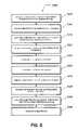
- FIG. 6illustrates the method as a flowchart 500 beginning in 505 with locating a substrate holder in a processing chamber at a first position within the deposition system.
- the first position for the substrate holderis located within a transfer space formed in a lower region of the processing chamber such that the substrate can be passed into and out of the processing chamber.
- the substrateis passed into the processing chamber through a transfer gate, and loaded onto the substrate holder.
- the substratemay be clamped and a backside gas may be provided to the backside of the substrate.
- the substrate holderis located at a second position within the deposition system.
- the second position for the substrate holderis located within a process space formed in an upper region of the processing chamber that is configured to treat the substrate.
- the substrate holderforms a seal with the processing chamber such that the process space is decoupled from the transfer space.
- the seal formed between the processing chamber and the substrate holdercan include a labyrinth seal.
- the transfer spaceis evacuated using a first pressure control system and, in 530 , the process space is evacuated using a second pressure control system.
- the first pressure control systemis configured to evacuate the transfer space of contaminants, operate at reduced pressure, and maintain a clean environment for substrate transfer.
- the second pressure control systemis configured to evacuate the process space, operate a reduced pressure, and provide a pressure suitable for the treatment of the substrate.
- the substrateis treated with a process.
- the processcan include a deposition process configured to form a thin film on the substrate using atomic layer deposition (ALD).
- ALDatomic layer deposition
- the process spacemay be purged, the transfer space may be purged, or both spaces may be purged.
- the substrate holderis located in the first position within the transfer space. During the translation of the substrate holder from the second position to the first position, the process space, or the transfer space, or both may be purged with a purge gas, such as an inert gas.
- the substrateis unloaded from the substrate holder and passed out of the processing chamber.
- FIG. 6Aillustrates in more detail an embodiment of steps 535 , 540 and 545 of FIG. 6 .
- the treating of the substrate in the process spacemay include, as in 536 , injecting gas from the first material source into the process space.
- This gasmay be TaCl 5 gas which adsorbs onto the surface of the substrate.
- this first materialmay be purged, as in 537 .
- gasmay be injected from the second material source into the process space.
- This gasmay be H 2 gas which reacts with the adsorbed TaCl 5 on the surface of the substrate, releasing the Cl.
- the process spacemay again be purged, as in 539 .
- Steps 536 through 539may be repeated, each time a mono-atomic layer (or fraction thereof) of coating, for example Ta, being deposited on the substrate.
- a mono-atomic layer (or fraction thereof) of coatingfor example Ta
- the upper chamber containing the process spaceis opened to the lower chamber while purge of the process space continues, so as to minimize progression of process gas to the lower chamber.
- the substrateis lowered into the lower chamber where additional purging may continue.
Landscapes
- Chemical & Material Sciences (AREA)
- Engineering & Computer Science (AREA)
- General Chemical & Material Sciences (AREA)
- Chemical Kinetics & Catalysis (AREA)
- Materials Engineering (AREA)
- Mechanical Engineering (AREA)
- Metallurgy (AREA)
- Organic Chemistry (AREA)
- Physics & Mathematics (AREA)
- Condensed Matter Physics & Semiconductors (AREA)
- General Physics & Mathematics (AREA)
- Manufacturing & Machinery (AREA)
- Computer Hardware Design (AREA)
- Microelectronics & Electronic Packaging (AREA)
- Power Engineering (AREA)
- Electromagnetism (AREA)
- Plasma & Fusion (AREA)
- Chemical Vapour Deposition (AREA)
Abstract
Description
1. Field of the Invention
The present invention relates to a plasma enhanced atomic layer deposition, and more particularly to a plasma enhanced atomic layer deposition system configured for reduced contamination and a method of operating the system.
2. Description of Related Art
Typically, during materials processing, when fabricating composite material structures, plasma is employed to facilitate the addition and removal of material films. For example, in semiconductor processing, a dry plasma etch process is often utilized to remove or etch material along fine lines or within vias or contacts patterned on a silicon substrate. Alternatively, for example, a vapor deposition process is utilized to deposit material along fine lines or within vias or contacts on a silicon substrate. In the latter, vapor deposition processes include chemical vapor deposition (CVD), and plasma enhanced chemical vapor deposition (PECVD).
In PECVD, plasma is utilized to alter or enhance the film deposition mechanism. For instance, plasma excitation generally allows film-forming reactions to proceed at temperatures that are significantly lower than those typically required to produce a similar film by thermally excited CVD. In addition, plasma excitation may activate film-forming chemical reactions that are not energetically or kinetically favored in thermal CVD. The chemical and physical properties of PECVD films may thus be varied over a relatively wide range by adjusting process parameters.
More recently, atomic layer deposition (ALD), a form of PECVD or more generally CVD, has emerged as a candidate for ultra-thin gate film formation in front end-of-line (FEOL) operations, as well as ultra-thin barrier layer and seed layer formation for metallization in back end-of-line (BEOL) operations. In ALD, two or more process gases are introduced alternatingly and sequentially in order to form a material film one monolayer at a time. Such an ALD process has proven to provide improved uniformity in layer thickness and conformality to features on which the layer is deposited.
CVD processes are generally regarded as “dirty” processes compared to PVD processes. CVD processes employ gases that are typically capable of forming deposits on various surfaces within a processing chamber and of escaping into adjacent passages and chambers, such as transport and adjacent processing chambers, to form deposits there. These deposits can flake off forming particulate contamination and can out-gas into the vacuum spaces to deposit elsewhere, including on wafers resting in or passing through those spaces. Such deposits can include films of the type being deposited on the wafer as well as deposits of other compounds formed by the CVD gases as a result of gas compositions, temperatures, energy levels and other factors existing at the surfaces of the various chamber components.
The problem of CVD gases escaping into adjacent chambers has been addressed by applicant's assignee in related U.S. Pat. No. 6,183,564, in which a buffer chamber is disclosed below a processing chamber in a CVD processing module. The buffer chamber is capable of being sealed from the processing chamber and is situated between the processing chamber and a transfer chamber so that the wafers pass through the buffer chamber when entering and leaving the process chamber. Dirty gases escaping from the processing chamber are trapped in and purged from the buffer chamber, thereby minimizing their contamination of the transfer chamber and chambers beyond.
With or without the use of the buffer chamber, after being processed, contaminants are found on wafers processed in the chamber. As features become smaller and films become thinner, this form of contamination is an increasing problem.
In accordance with certain principles of the present invention, a plasma enhanced atomic layer deposition (PEALD) system and a method of operating thereof is provided.
In an embodiment of the present invention, a method and system is provided for reducing contamination in a plasma enhanced atomic layer deposition (PEALD) system.
According to another embodiment, a deposition system for forming a thin film on a substrate is described comprising: a processing chamber comprising a process space in an upper region of the processing chamber configured to facilitate the thin film deposition, and a transfer space in a lower region of the processing chamber configured to facilitate transfer of the substrate into and out of the processing chamber; a substrate holder coupled to the processing chamber and configured to support the substrate, and configured to translate vertically between a first position to locate the substrate in the transfer space and a second position to locate the substrate in the process space, wherein the substrate holder comprises a sealing device configured to seal the substrate holder with the processing chamber when the substrate holder is in the second position; a first pressure control system coupled to the transfer space and configured to provide a substantially contaminant-free environment in the transfer space; a second pressure control system coupled to the process space and configured to evacuate the process space during processing; a gas injection system coupled to the processing chamber, and configured to alternatingly introduce a first process material and a second process material to the process space; a power source coupled to the processing chamber, and configured to couple power to the first process material, or the second process material, or both in the process space to facilitate the formation of plasma; and a temperature control system coupled to the substrate holder, and configured to control a temperature of the substrate.
According to yet another embodiment, a method of treating a substrate in a deposition system is described comprising: locating a substrate holder at a first position within a transfer space of a processing chamber of the deposition system; loading the substrate onto the substrate holder while the substrate holder is in the first position; locating the substrate holder within the processing chamber at a second position within a process space of the processing chamber; sealing the substrate holder with the processing chamber while the substrate holder is in the second position such that the process space is decoupled from the transfer space; evacuating the transfer space using a first pressure control system; evacuating the process space using a second pressure control system; treating the substrate in the process space by alternatingly exposing the substrate to a first process material and a second process material, and forming plasma during the exposing of the substrate to the second process material; relocating the substrate holder at the first position; and unloading the substrate when the substrate holder is at the first position. When relocating the substrate to the first position, the substrate holder is unsealed from the processing chamber and moved from the second position such that the process space is recoupled to the transfer space, and the pressure and flow within the processing chamber and transfer space are controlled to reduce the tendency of contaminant producing materials from entering the transfer space from the process chamber.
According to yet another embodiment, a deposition system for forming a thin film on a substrate is described comprising: a processing chamber comprising a process space in an upper region of the processing chamber configured to facilitate the thin film deposition, and a transfer space in a lower region of the processing chamber configured to facilitate transfer of the substrate into and out of the processing chamber; a substrate holder coupled to the processing chamber and configured to support the substrate, and configured to translate vertically between a first position to locate the substrate in the transfer space and a second position to locate the substrate in the process space, wherein the substrate holder comprises a sealing device configured to seal the substrate holder with the processing chamber when the substrate holder is in the second position; means for controlling the pressure in the transfer space in order to provide a substantially contaminant-free environment in the transfer space; means for controlling the pressure in the process space in order to evacuate the process space during processing; means for alternatingly introducing a first process material and a second process material to the process space; means for coupling power to the processing chamber in order to couple power to the first process material, or the second process material, or both in the process space to facilitate the formation of plasma; and means for controlling the temperature of the substrate.
In the accompanying drawings:
In the following description, in order to facilitate a thorough understanding of the invention and for purposes of explanation and not limitation, specific details are set forth, such as a particular geometry of the deposition system and descriptions of various components. However, it should be understood that the invention may be practiced in other embodiments that depart from these specific details.
Referring now to the drawings, wherein like reference numerals designate identical or corresponding parts throughout the several views,FIG. 1 illustrates adeposition system 10 for depositing a thin film, such as a barrier film, on a substrate using plasma enhanced atomic layer deposition (PEALD). For example, during the metallization of inter-connect and intra-connect structures for semiconductor devices in back-end-of-line (BEOL) operations, a thin conformal barrier layer may be deposited on wiring trenches or vias to minimize the migration of metal into the inter-level or intra-level dielectric, or a thin conformal seed layer may be deposited on wiring trenches or vias to provide a film with acceptable adhesion properties for bulk metal fill, or a thin conformal adhesion layer may be deposited on wiring trenches or vias to provide a film with acceptable adhesion properties for metal seed deposition. Thedeposition system 10 comprises aprocessing chamber 11 having asubstrate holder 20 configured to support asubstrate 25, upon which the thin film is formed. Theprocessing chamber 11 further comprises anupper chamber assembly 30 coupled to a first processmaterial supply system 40, a second processmaterial supply system 42, and a purgegas supply system 44. Additionally, thedeposition system 10 comprises afirst power source 50 coupled to theprocessing chamber 11 and configured to generate plasma in theprocessing chamber 11, and a substratetemperature control system 60 coupled tosubstrate holder 20 and configured to elevate and control the temperature ofsubstrate 25. Additionally,deposition system 10 comprises acontroller 70 that can be coupled toprocessing chamber 11,substrate holder 20,upper assembly 30, first processmaterial supply system 40, second processmaterial supply system 42, purgegas supply system 44,first power source 50, and substratetemperature control system 60.
Thedeposition system 10 may be configured to process 200 mm substrates, 300 mm substrates, or larger-sized substrates. In fact, it is contemplated that the deposition system may be configured to process substrates, wafers, or LCDs regardless of their size, as would be appreciated by those skilled in the art. Substrates can be introduced toprocessing chamber 11, and they may be lifted to and from an upper surface ofsubstrate holder 20 via substrate lift system (not shown).
The first processmaterial supply system 40 and the second processmaterial supply system 42 are configured to alternatingly introduce a first process material toprocessing chamber 11 and a second process material toprocessing chamber 11. The alternation of the introduction of the first process material and the introduction of the second process material can be cyclical, or it may be acyclical with variable time periods between introduction of the first and second process materials. The first process material can, for example, comprise a film precursor, such as a composition having the principal atomic or molecular species found in the film formed onsubstrate 25. For instance, the film precursor can originate as a solid phase, a liquid phase, or a gaseous phase, and it may be delivered toprocessing chamber 11 in a gaseous phase. The second process material can, for example, comprise a reducing agent. For instance, the reducing agent can originate as a solid phase, a liquid phase, or a gaseous phase, and it may be delivered to processingchamber 11 in a gaseous phase.
Additionally, the purgegas supply system 44 can be configured to introduce a purge gas toprocessing chamber 11 between introduction of the first process material and the second process material toprocessing chamber 11, respectively. The purge gas can comprise an inert gas, such as a Noble gas (i.e., helium, neon, argon, xenon, krypton).
Referring still toFIG. 1 , thedeposition system 10 comprises a plasma generation system configured to generate a plasma during at least a portion of the alternating introduction of the first process material and the second process material toprocessing chamber 11. The plasma generation system can include afirst power source 50 coupled to theprocessing chamber 11, and configured to couple power to the first process material, or the second process material, or both inprocessing chamber 11. Thefirst power source 50 may include a radio frequency (RF) generator and an impedance match network (not shown), and may further include an electrode (not shown) through which RF power is coupled to plasma inprocessing chamber 11. The electrode can be formed in theupper assembly 30, and it can be configured to oppose thesubstrate holder 20. The impedance match network can be configured to optimize the transfer of RF power from the RF generator to the plasma by matching the output impedance of the match network with the input impedance of the processing chamber, including the electrode, and plasma. For instance, the impedance match network serves to improve the transfer of RF power to plasma inplasma processing chamber 11 by reducing the reflected power. Match network topologies (e.g. L-type, π-type, T-type, etc.) and automatic control methods are well known to those skilled in the art.
Optionally, thedeposition system 10 comprises a substrate bias generation system configured to generate a plasma during at least a portion of the alternating and cyclical introduction of the first process material and the second process material to processingchamber 11. The substrate bias system can include asecond power source 52 coupled to theprocessing chamber 11, and configured to couple power tosubstrate 25. Thesecond power source 52 may include a radio frequency (RF) generator and an impedance match network, and may further include an electrode through which RF power is coupled tosubstrate 25. The electrode can be formed insubstrate holder 20. For instance,substrate holder 20 can be electrically biased at an RF voltage via the transmission of RF power from an RF generator (not shown) through an impedance match network (not shown) tosubstrate holder 20. A typical frequency for the RF bias can range from about 0.1 MHz to about 100 MHz. RF bias systems for plasma processing are well known to those skilled in the art. Alternately, RF power is applied to the substrate holder electrode at multiple frequencies.
Although the plasma generation system and the optional substrate bias system are illustrated inFIG. 1 as separate entities, they may comprise one or more power sources coupled tosubstrate holder 20.
Still referring toFIG. 1 ,deposition system 10 comprises substratetemperature control system 60 coupled to thesubstrate holder 20 and configured to elevate and control the temperature ofsubstrate 25. Substratetemperature control system 60 comprises temperature control elements, such as a cooling system including a re-circulating coolant flow that receives heat fromsubstrate holder 20 and transfers heat to a heat exchanger system (not shown), or when heating, transfers heat from the heat exchanger system. Additionally, the temperature control elements can include heating/cooling elements, such as resistive heating elements, or thermoelectric heaters/coolers can be included in thesubstrate holder 20, as well as the chamber wall of theprocessing chamber 11 and any other component within thedeposition system 10.
In order to improve the thermal transfer betweensubstrate 25 andsubstrate holder 20,substrate holder 20 can include a mechanical clamping system, or an electrical clamping system, such as an electrostatic clamping system, to affixsubstrate 25 to an upper surface ofsubstrate holder 20. Furthermore,substrate holder 20 can further include a substrate backside gas delivery system configured to introduce gas to the backside ofsubstrate 25 in order to improve the gas-gap thermal conductance betweensubstrate 25 andsubstrate holder 20. Such a system can be utilized when temperature control of the substrate is required at elevated or reduced temperatures. For example, the substrate backside gas system can comprise a two-zone gas distribution system, wherein the helium gas gap pressure can be independently varied between the center and the edge ofsubstrate 25.
Furthermore, theprocessing chamber 11 is further coupled to apressure control system 32, including avacuum pumping system 34 and avalve 36, through aduct 38, wherein thepressure control system 34 is configured to controllably evacuate theprocessing chamber 11 to a pressure suitable for forming the thin film onsubstrate 25, and suitable for use of the first and second process materials.
Thevacuum pumping system 34 can include a turbo-molecular vacuum pump (TMP) capable of a pumping speed up to about 5000 liters per second (and greater) andvalve 36 can include a gate valve for throttling the chamber pressure. In conventional plasma processing devices utilized for dry plasma etch, a 1000 to 3000 liter per second TMP is generally employed. Moreover, a device for monitoring chamber pressure (not shown) can be coupled to theprocessing chamber 110. The pressure measuring device can be, for example, a Type 628B Baratron absolute capacitance manometer commercially available from MKS Instruments, Inc. (Andover, Mass.).
Still referring toFIG. 1 ,controller 70 can comprise a microprocessor, memory, and a digital I/O port capable of generating control voltages sufficient to communicate and activate inputs todeposition system 10 as well as monitor outputs fromdeposition system 10. Moreover, thecontroller 70 may exchange information with theprocessing chamber 11,substrate holder 20,upper assembly 30, first processmaterial supply system 40, second processmaterial supply system 42, purgegas supply system 44,first power source 50,second power source 52, substratetemperature control system 60, andpressure control system 32. For example, a program stored in the memory may be utilized to activate the inputs to the aforementioned components of thedeposition system 10 according to a process recipe in order to perform an etching process, or a deposition process. One example of thecontroller 70 is a DELL PRECISION WORKSTATION 610, available from Dell Corporation, Austin, Tex.
Referring now toFIG. 2 , anotherdeposition system 101 is depicted. Thedeposition system 101 comprises aprocessing chamber 110 having asubstrate holder 120 configured to support asubstrate 125, upon which the thin film is formed. Theprocessing chamber 110 further comprises anupper assembly 130 coupled to a first processmaterial supply system 140, a second processmaterial supply system 142, and a purgegas supply system 144. Additionally, thedeposition system 101 comprises afirst power source 150 coupled to theprocessing chamber 110 and configured to generate plasma in theprocessing chamber 110, and a substratetemperature control system 160 coupled tosubstrate holder 120 and configured to elevate and control the temperature ofsubstrate 125. Additionally,deposition system 101 comprises acontroller 170 that can be coupled toprocessing chamber 110,substrate holder 120,upper assembly 130, first processmaterial supply system 140, second processmaterial supply system 142, purgegas supply system 144,first power source 150, and substratetemperature control system 160.
Thedeposition system 101 may be configured to process 200 mm substrates, 300 mm substrates, or larger-sized substrates. In fact, it is contemplated that the deposition system may be configured to process substrates, wafers, or LCDs regardless of their size, as would be appreciated by those skilled in the art. Substrates can be introduced toprocessing chamber 110 throughpassage 112, and they may be lifted to and from an upper surface ofsubstrate holder 120 viasubstrate lift system 122. Thepassage 112 may be sealable with a gate valve (not shown).
The first processmaterial supply system 140 and the second processmaterial supply system 142 are configured to alternatingly introduce a first process material toprocessing chamber 110 and a second process material toprocessing chamber 110. The alternation of the introduction of the first process material and the introduction of the second process material can be cyclical, or it may be acyclical with variable time periods between introduction of the first and second process materials. The first process material can, for example, comprise a film precursor, such as a composition having the principal atomic or molecular species found in the film formed onsubstrate 125. For instance, the film precursor can originate as a solid phase, a liquid phase, or a gaseous phase, and it may be delivered toprocessing chamber 110 in a gaseous phase. The second process material can, for example, comprise a reducing agent. For instance, the reducing agent can originate as a solid phase, a liquid phase, or a gaseous phase, and it may be delivered toprocessing chamber 110 in a gaseous phase. In one example, during the deposition of tantalum (Ta) as a barrier layer, the first process material can include a solid film precursor, such as TaCl5, and the second process material can include a reducing agent, such as hydrogen (H2) gas. In another example, during the deposition of tantalum nitride (TaN) or tantalum carbonitride (TaCN) as a barrier layer, the first process material can include a metal organic film precursor, such as tertiary amyl imido-tris-dimethylamido tantalum (Ta(NC(CH3)2C2H5)(N(CH3)2)3, hereinafter referred to as TAIMATA), and the second process material can include a reducing agent, such as hydrogen (H2), ammonia (NH3), silane (SiH4), or disilane (Si2H6), or a combination thereof.
Additionally, the purgegas supply system 144 can be configured to introduce a purge gas to processingchamber 110 between introduction of the first process material and the second process material toprocessing chamber 110, respectively. The purge gas can comprise an inert gas, such as a Noble gas (i.e., helium, neon, argon, xenon, krypton).
The firstmaterial supply system 140, the secondmaterial supply system 142, and the purgegas supply system 144 can include one or more material sources, one or more pressure control devices, one or more flow control devices, one or more filters, one or more valves, or one or more flow sensors.
Referring still toFIG. 2 , the first process material is coupled toprocessing chamber 110 throughfirst material line 141, and the second process material is coupled toprocessing chamber 110 throughsecond material line 143. Additionally, the purge gas may be coupled toprocessing chamber 110 through the first material line141 (as shown), the second material line143 (as shown), or an independent line, or any combination thereof. The first process material, second process material, and purge gas are introduced and distributed withinprocessing chamber 110 through theupper assembly 130 that includesgas injection assembly 180. Thegas injection assembly 180 may comprise afirst injection plate 182, asecond injection plate 184, and athird injection plate 186, which are electrically insulated from processingchamber 110 byinsulation assembly 188. The first process material is coupled from the first processmaterial supply system 140 toprocessing chamber 110 through a first array of through-holes 194 in thesecond injection plate 184 and a first array oforifices 195 in thefirst injection plate 182 via afirst plenum 190 formed between thesecond injection plate 184 and thethird injection plate 186. The second process material, or purge gas, or both is coupled from the second processmaterial supply system 142 or purgegas supply system 144 toprocessing chamber 110 through a second array oforifices 197 in thefirst injection plate 182 via asecond plenum 192 formed in thesecond injection plate 184.
Referring still toFIG. 2 , thedeposition system 101 comprises a plasma generation system configured to generate a plasma during at least a portion of the alternating and cyclical introduction of the first process material and the second process material toprocessing chamber 110. The plasma generation system can include afirst power source 150 coupled to theprocessing chamber 110, and configured to couple power to the first process material, or the second process material, or both inprocessing chamber 110. Thefirst power source 150 includes a radio frequency (RF) generator154 and animpedance match network 156, and further includes an electrode, such asgas injection assembly 180, through which RF power is coupled to plasma inprocessing chamber 110. The electrode is formed in theupper assembly 130 and is insulated from processingchamber 110 viainsulation assembly 188, and it can be configured to oppose thesubstrate holder 120. The RF frequency can, for example, range from approximately 100 kHz to approximately 100 MHz. Alternatively, the RF frequency can, for example, range from approximately 400 kHz to approximately 60 MHz. By way of further example, the RF frequency can, for example, be approximately 27.12 MHz.
Still referring toFIG. 2 ,deposition system 101 comprises substratetemperature control system 160 coupled to thesubstrate holder 120 and configured to elevate and control the temperature ofsubstrate 125. Substratetemperature control system 160 comprises at least one temperature control element, including a resistive heating element such as an aluminum nitride heater. The substratetemperature control system 160 can, for example, be configured to elevate and control the substrate temperature up to approximately 400 degrees C. Alternatively, the substrate temperature can, for example, range from approximately 150 degrees C. to 350 degrees C.
Furthermore, theprocessing chamber 110 is further coupled to apressure control system 132, including avacuum pumping system 134 and avalve 136, through aduct 138, wherein thepressure control system 134 is configured to controllably evacuate theprocessing chamber 110 to a pressure suitable for forming the thin film onsubstrate 125, and suitable for use of the first and second process materials.
Referring now toFIG. 3 ,deposition system 101 can be configured to perform a plasma enhanced atomic layer deposition (PEALD) process. For example, in a PEALD process for preparing a thin, conformal, tantalum-containing film, a first process material comprising tantalum, such as tantalum pentachloride or TAIMATA, is introduced toprocessing chamber 110 for a first period of time in order to cause adsorption of the film precursor (first process material) on exposed surfaces ofsubstrate 125, then processingchamber 110 is purged with a purge gas for a second period of time. Thereafter, a reducing agent (second process material), such as hydrogen, is introduced toprocessing chamber 110 for a third period of time while power is coupled through theupper assembly 130 from thefirst power source 150 to the reducing agent. The coupling of power to the reducing agent heats the reducing agent, thus causing ionization and dissociation of the reducing agent in order to form, for example, atomic hydrogen, which chemically reacts with the first precursor adsorbed onsubstrate 125. Whensubstrate 125 is heated to an elevated temperature, the surface chemical reaction facilitates the formation of the desired tantalum containing film. Theprocessing chamber 110 is purged with a purge gas for a fourth period of time. The introduction of the first process material and the second process material, and the formation of plasma can be repeated any number of times to produce a film of desired thickness.
As described above in reference toFIGS. 1 and 2 , a deposition system is described for performing a PEALD process as illustrated inFIG. 3 . In the deposition system(s) described inFIGS. 1 and 2 , the substrate is processed, as well as transferred into and out of the processing chamber in the same space. It has been observed by the inventors that following processing of the substrate, i.e., the deposition of a thin film, the substrate may encounter contamination during transfer out of the processing chamber. For example, when depositing tantalum (Ta), the first process material can include a halogen containing material, such as tantalum pentachloride, and the second process material can include hydrogen, whereby a hydrogen plasma is formed to generate hydrogen radical to reduce the adsorbed tantalum pentachloride on the substrate surface. During the process, chlorine can accumulate within internal surfaces of the processing chamber. Thereafter, following processing when the substrate is transferred out of the processing chamber, the film deposited on the substrate, already potentially containing residual chlorine, can become further contaminated with chlorine remaining in the processing chamber. The inventors have observed that chlorine-contaminated films lead to additional problems in the following process steps, such as copper agglomeration during metal seed formation for feature metallization.
According to an embodiment, adeposition system 201 is provided inFIG. 4 , which is configured to reduce substrate contamination during substrate treatment and transfer. Thedeposition system 201 comprises aprocessing chamber 210 having aprocess space 212 in anupper region 214 ofprocessing chamber 210 configured to facilitate thin film deposition on asubstrate 225, and atransfer space 216 in alower region 218 ofprocessing chamber 210 configured to facilitate transfer ofsubstrate 225 into and out ofprocessing chamber 210.
Thedeposition system 201 further comprises asubstrate holder 220 coupled toprocessing chamber 210 and configured to support asubstrate 225, upon which the thin film is formed. Thesubstrate holder 220 is further configured to translate vertically between afirst position 222 to locate thesubstrate 225 in the transfer space216 (seeFIG. 5 ) and asecond position 224 to locate thesubstrate 225 in the process space212 (seeFIG. 4 ). Thesubstrate holder 220 includes asealing device 226 and adrive system 228. The sealing device is configured to seal thesubstrate holder 220 with theprocessing chamber 210 when thesubstrate holder 220 is in thesecond position 224. Thedrive system 228 is configured to translate thesubstrate holder 220. As illustrated inFIGS. 4 and 5 , thesealing device 226 may comprise a labyrinth seal having a first set ofteeth 227 coupled to an outer edge of thesubstrate holder 220 configured to mate with a second set ofteeth 229 coupled to an inner edge of the upper region of theprocessing chamber 210 when thesubstrate holder 220 is located in thesecond position 224 such that thesubstrate 225 is in theprocess space 212. Alternatively, thesealing device 226 can comprise at least one (elastomer) O-ring seal coupled to thesubstrate holder 220, or theprocessing chamber 210, or both. Alternatively, other seals may be provided.
Theprocessing chamber 210 further comprises anupper assembly 230 coupled to a first processmaterial supply system 240, a second processmaterial supply system 242, and a purgegas supply system 244. Additionally, thedeposition system 201 comprises afirst power source 250 coupled to theprocessing chamber 210 and configured to generate plasma in theprocessing chamber 210, and a substratetemperature control system 260 coupled tosubstrate holder 220 and configured to elevate and control the temperature ofsubstrate 225. Additionally,deposition system 201 comprises acontroller 270 that can be coupled toprocessing chamber 210,substrate holder 220,upper assembly 230, first processmaterial supply system 240, second processmaterial supply system 242, purgegas supply system 244,first power source 250, and substratetemperature control system 260.
Alternately, or in addition,controller 270 can be coupled to a one or more additional controllers/computers (not shown), andcontroller 270 can obtain setup and/or configuration information from an additional controller/computer.
InFIGS. 4 and 5 , singular processing elements (210,220,230,240,242,244,250, and260) are shown, but this is not required for the invention. Thedeposition system 201 can comprise any number of processing elements having any number of controllers associated with them in addition to independent processing elements.
Thecontroller 270 can be used to configure any number of processing elements (210,220,230,240,242,244,250, and260), and thecontroller 270 can collect, provide, process, store, and display data from processing elements. Thecontroller 270 can comprise a number of applications for controlling one or more of the processing elements. For example,controller 270 can include a graphic user interface (GUI) component (not shown) that can provide easy to use interfaces that enable a user to monitor and/or control one or more processing elements.
Thedeposition system 201 may be configured to process 200 mm substrates, 300 mm substrates, or larger-sized substrates. In fact, it is contemplated that the deposition system may be configured to process substrates, wafers, or LCDs regardless of their size, as would be appreciated by those skilled in the art. Substrates can be introduced toprocessing chamber 210 throughpassage 212, and they may be lifted to and from an upper surface ofsubstrate holder 220 via a substrate lift system.
The first processmaterial supply system 240 and the second processmaterial supply system 242 are configured to alternatingly introduce a first process material toprocessing chamber 210 and a second process material toprocessing chamber 210. The alternation of the introduction of the first process material and the introduction of the second process material can be cyclical, or it may be acyclical with variable time periods between introduction of the first and second process materials. The first process material can, for example, comprise a film precursor, such as a composition having the principal atomic or molecular species found in the film formed onsubstrate 225. For instance, the film precursor can originate as a solid phase, a liquid phase, or a gaseous phase, and it may be delivered toprocessing chamber 210 in a gaseous phase. The second process material can, for example, comprise a reducing agent. For instance, the reducing agent can originate as a solid phase, a liquid phase, or a gaseous phase, and it may be delivered toprocessing chamber 210 in a gaseous phase. In one example, during the deposition of tantalum (Ta) as a barrier layer, the first process material can include a solid film precursor, such as TaCl5, and the second process material can include a reducing agent, such as hydrogen (H2) gas. In another example, during the deposition of tantalum nitride (TaN) or tantalum carbonitride (TaCN) as a barrier layer, the first process material can include a metal organic film precursor, such as TAIMATA, and the second process material can include a reducing agent, such as hydrogen (H2), ammonia (NH3), silane (SiH4), or disilane (Si2H6), or a combination thereof.
In another example, when depositing tantalum (Ta), tantalum nitride, or tantalum carbonitride, the first process material can include TaF5, TaCl5, TaBr5, Tal5, Ta(CO)5, Ta[N(C2H5CH3)]5(PEMAT), Ta[N(CH3)2]5(PDMAT), Ta[N(C2H5)2]5(PDEAT), Ta(NC(CH3)3)(N(C2H5)2)3(TBTDET), Ta(NC2H5)(N(C2H5)2)3, Ta(NC(CH3)2C2H5)(N(CH3)2)3, or Ta(NC(CH3)3)(N(CH3)2)3, and the second process material can include H2, NH3, N2and H2, N2H4, NH(CH3)2, or N2H3CH3.
In another example, when depositing titanium (Ti), titanium nitride, or titanium carbonitride, the first process material can include TiF4, TiCl4, TiBr4, Til4, Ti[N(C2H5CH3)]4(TEMAT), Ti[N(CH3)2]4(TDMAT), or Ti[N(C2H5)2]4(TDEAT), and the second process material can include H2, NH3, N2and H2, N2H4, NH(CH3)2, or N2H3CH3.
As another example, when depositing tungsten (W), tungsten nitride, or tungsten carbonitride, the first process material can include WF6, or W(CO)6, and the second process material can include H2, NH3, N2and H2, N2H4, NH(CH3)2, or N2H3CH3.
Additionally, the purgegas supply system 244 can be configured to introduce a purge gas to processingchamber 210 between introduction of the first process material and the second process material toprocessing chamber 210, respectively. The purge gas can be introduced to either thetransfer space 216, or theprocess space 212, or both. The purge gas can comprise an inert gas, such as a Noble gas (i.e., helium, neon, argon, xenon, krypton).
The firstmaterial supply system 240, the secondmaterial supply system 242, and the purgegas supply system 244 can include one or more material sources, one or more pressure control devices, one or more flow control devices, one or more filters, one or more valves, or one or more flow sensors.
Referring still toFIGS. 4 and 5 , thedeposition system 201 comprises a plasma generation system configured to generate plasma during at least a portion of the alternating and cyclical introduction of the first process material and the second process material toprocessing chamber 210. The plasma generation system can include afirst power source 250 coupled to theprocessing chamber 210, and configured to couple power to the first process material, or the second process material, or both inprocessing chamber 210. For example, thefirst power source 250 may be coupled to thesubstrate holder 220 as depicted inFIGS. 4 and 5 . Thefirst power source 250 includes a radio frequency (RF)generator 254 and animpedance match network 252, and further includes anelectrode 256, formed withinsubstrate holder 220, through which RF power is coupled to plasma inprocessing chamber 210. The RF frequency can, for example, range from approximately 100 kHz to approximately 100 MHz. Alternatively, the RF frequency can, for example, range from approximately 400 kHz to approximately 60 MHz. By way of further example, the RF frequency can, for example, be approximately 27.12 MHz.
Alternatively, the plasma generation system can include asecond power source 280 coupled to theprocessing chamber 210, and configured to couple power to the first process material, or the second process material, or both inprocessing chamber 210. For example, thesecond power source 280 may be coupled to theupper assembly 230 as depicted inFIGS. 4 and 5 . Thesecond power source 280 includes a radio frequency (RF)generator 284 and animpedance match network 282, and further includes an electrode286, formed withinupper assembly 230, through which RF power is coupled to plasma inprocessing chamber 210. The electrode is formed in theupper assembly 230 and is insulated from processingchamber 210 via an insulation assembly (not shown), and it can be configured to oppose thesubstrate holder 220.
Alternatively, the plasma generation system includes both thefirst power source 250 and thesecond power source 280, which can be utilized to generate plasma andbias substrate 225.
Alternatively, thesecond power source 280 may include a radio frequency (RF) generator and an impedance match network, and may further include an antenna, such as an inductive coil, through which RF power is coupled to plasma inprocessing chamber 210. The antenna can, for example, include a helical or solenoidal coil, such as in an inductively coupled plasma source or helicon source, or it can, for example, include a flat coil as in a transformer coupled plasma source.
Alternatively, thesecond power source 280 may include a microwave frequency generator, and may further include a microwave antenna and microwave window through which microwave power is coupled to plasma inprocessing chamber 210. The coupling of microwave power can be accomplished using electron cyclotron resonance (ECR) technology, or it may be employed using surface wave plasma technology, such as a slotted plane antenna (SPA), as described in U.S. Pat. No. 5,024,716, entitled “Plasma processing apparatus for etching, ashing, and film-formation”; the contents of which are herein incorporated by reference in its entirety.
Still referring toFIGS. 4 and 5 ,deposition system 201 comprises a substratetemperature control system 260 coupled to thesubstrate holder 220 and configured to elevate and control the temperature ofsubstrate 225. Substratetemperature control system 260 comprises at least one temperature control element, including a resistive heating element such as an aluminum nitride heater. The substratetemperature control system 260 can, for example, be configured to elevate and control the substrate temperature up to approximately 400 degrees C. Alternatively, the substrate temperature can, for example, range from approximately 150 degrees C. to 350 degrees C.
In order to improve the thermal transfer betweensubstrate 225 andsubstrate holder 220,substrate holder 220 can include a mechanical clamping system, or an electrical clamping system, such as anelectrostatic clamping system 264, to affixsubstrate 225 to an upper surface ofsubstrate holder 220. Furthermore,substrate holder 220 can further include a substrate backside gas delivery system (not shown) configured to introduce gas to the backside ofsubstrate 225 in order to improve the gas-gap thermal conductance betweensubstrate 225 andsubstrate holder 220. Such a system can be utilized when temperature control of the substrate is required at elevated or reduced temperatures. For example, the substrate backside gas system can comprise a two-zone gas distribution system, wherein the helium gas gap pressure can be independently varied between the center and the edge ofsubstrate 225.
Furthermore, thetransfer space 216 of thelower region 218 inprocessing chamber 210 is coupled to a firstpressure control system 290, and theprocess space 212 in theupper region 214 ofprocessing chamber 210 is coupled to a secondpressure control system 292. The firstpressure control system 290 can comprise afirst valve 294 and a firstvacuum pumping system 295 configured to evacuate thetransfer space 216 and control the pressure intransfer space 218. Additionally, the secondpressure control system 292 can include asecond valve 296 and a secondvacuum pumping system 297 configured to controllably evacuate theprocessing chamber 210 to a pressure suitable for forming the thin film onsubstrate 225, and suitable for use of the first and second process materials. The first andsecond valves vacuum pumping system 295 can, for instance, comprise a cryogenic vacuum pump. The secondvacuum pumping system 297 can, for instance, comprise a turbo-molecular vacuum pump (TMP) capable of a pumping speed up to about 5000 liters per second (and greater). In conventional plasma processing devices, a 1000 to 3000 liter per second TMP is generally employed. Moreover, a device for monitoring chamber pressure (not shown) inprocess space 212 can be coupled to theprocessing chamber 210. The pressure measuring device can be, for example, a Type 628B Baratron absolute capacitance manometer commercially available from MKS Instruments, Inc. (Andover, Mass.).
Referring still toFIGS. 4 and 5 , thedeposition system 201 further comprises atransfer gate 300 coupled to thelower region 218 ofprocessing chamber 210. Thetransfer gate 300 can open and close in order to permit access to thetransfer space 216 of theprocessing chamber 210 and allow the passing ofsubstrate 225 into and out of theprocessing chamber 210. During the opening and closing oftransfer gate 300, theprocessing chamber 210, or the transfer system to which the processing chamber is coupled, or both may be pressure controlled, purged with a gas, or differentially pumped, or any combination thereof.
Still referring toFIGS. 4 and 5 ,control system 270 can comprise a microprocessor, memory, and a digital I/O port capable of generating control voltages sufficient to communicate and activate inputs todeposition system 201 as well as monitor outputs fromdeposition system 201. Moreover, thecontroller 270 may be coupled to and may exchange information with theprocessing chamber 210,substrate holder 220,upper assembly 230, first processmaterial supply system 240, second processmaterial supply system 242, purgegas supply system 244,first power source 250,second power source 280, substratetemperature control system 260, firstpressure control system 290, secondpressure control system 292, and thetransfer gate 300. For example, a program stored in the memory may be utilized to activate the inputs to the aforementioned components of thedeposition system 201 according to a process recipe in order to perform an etching process, or a deposition process. One example of thecontroller 270 is a DELL PRECISION WORKSTATION 610, available from Dell Corporation, Austin, Tex.
Thecontroller 270 may be locally located relative to thedeposition system 201, or it may be remotely located relative to thedeposition system 201. For example, thecontroller 270 may exchange data with thedeposition 201 using at least one of a direct connection, an intranet, the Internet and a wireless connection. Thecontroller 270 may be coupled to an intranet at, for example, a customer site (i.e., a device maker, etc.), or it may be coupled to an intranet at, for example, a vendor site (i.e., an equipment manufacturer). Additionally, for example, thecontroller 270 may be coupled to the Internet. Furthermore, another computer (i.e., controller, server, etc.) may access, for example, thecontroller 270 to exchange data via at least one of a direct connection, an intranet, and the Internet. As also would be appreciated by those skilled in the art, thecontroller 270 may exchange data with thedeposition system 201 via a wireless connection.
According to yet another embodiment, a method of operating a deposition system, such as the system described in reference toFIGS. 4 and 5 , is presented.FIG. 6 illustrates the method as aflowchart 500 beginning in505 with locating a substrate holder in a processing chamber at a first position within the deposition system. The first position for the substrate holder is located within a transfer space formed in a lower region of the processing chamber such that the substrate can be passed into and out of the processing chamber. In510, once the substrate holder is located in the first position within the transfer space, the substrate is passed into the processing chamber through a transfer gate, and loaded onto the substrate holder. When the substrate is loaded onto the substrate holder, the substrate may be clamped and a backside gas may be provided to the backside of the substrate.
Following the loading of the substrate, in515, the substrate holder is located at a second position within the deposition system. The second position for the substrate holder is located within a process space formed in an upper region of the processing chamber that is configured to treat the substrate. In520, when the substrate holder is located in the second position, the substrate holder forms a seal with the processing chamber such that the process space is decoupled from the transfer space. For example, the seal formed between the processing chamber and the substrate holder can include a labyrinth seal.
In525, the transfer space is evacuated using a first pressure control system and, in530, the process space is evacuated using a second pressure control system. The first pressure control system is configured to evacuate the transfer space of contaminants, operate at reduced pressure, and maintain a clean environment for substrate transfer. The second pressure control system is configured to evacuate the process space, operate a reduced pressure, and provide a pressure suitable for the treatment of the substrate.
In535, the substrate is treated with a process. For example, the process can include a deposition process configured to form a thin film on the substrate using atomic layer deposition (ALD). In540, once the process for treating the substrate is complete, the process space may be purged, the transfer space may be purged, or both spaces may be purged. In545, the substrate holder is located in the first position within the transfer space. During the translation of the substrate holder from the second position to the first position, the process space, or the transfer space, or both may be purged with a purge gas, such as an inert gas.
In550, the substrate is unloaded from the substrate holder and passed out of the processing chamber.
Although only certain exemplary embodiments of this invention have been described in detail above, those skilled in the art will readily appreciate that many modifications are possible in the exemplary embodiments without materially departing from the novel teachings and advantages of this invention. Accordingly, all such modifications are intended to be included within the scope of this invention.
Claims (21)
1. An atomic layer deposition system for forming a thin film on a substrate comprising:
a processing chamber comprising a process space in an upper region of said processing chamber configured to facilitate said thin film deposition, and a transfer space in a lower region of said processing chamber having an opening to the upper region at the top thereof, the lower region being configured to facilitate transfer of said substrate into and out of the upper region of said processing chamber;
a substrate holder coupled to said processing chamber and configured to support said substrate and to translate vertically between a first position to locate said substrate in said transfer space and a second position to locate said substrate in said process space, said substrate holder comprising a sealing device configured to seal said substrate holder with said processing chamber to seal the opening and to isolate the transfer space from the process space when said substrate holder is in said second position;
at least two pressure control systems, including:
a first pressure control system coupled to said transfer space and configured to provide a substantially contaminant-free environment in said transfer space when isolated from said process space by the sealing member of the substrate holder when in said second position;
a second pressure control system coupled to said process space and configured to evacuate said process space during processing;
a gas injection system coupled to the upper region of said processing chamber, and configured to alternatingly introduce a first process material and a second process material to said process space;
a power source coupled to said processing chamber, and configured to couple power to said first process material, or said second process material, or both in said process space to facilitate the formation of plasma;
a temperature control system coupled to said substrate holder, and configured to control a temperature of said substrate; and
a process controller operable to control the deposition system to perform a plasma-enhanced atomic layer deposition process on the substrate.
2. The deposition system ofclaim 1 , wherein said deposition system is coupled to a transfer system configured to transport said substrate into said transfer space of said processing chamber through a gate valve coupled to said lower region of said processing chamber.
3. The deposition system ofclaim 1 , wherein said sealing device comprises a labyrinth seal formed between an outer edge of said substrate holder and an inner edge of said upper region of said processing chamber.
4. The deposition system ofclaim 3 , wherein said labyrinth seal comprises a first set of teeth coupled to said substrate holder and configured to mate with a second set of teeth coupled to said processing chamber when said substrate holder is located in said second position.
5. The deposition system ofclaim 1 , wherein said sealing device comprises at least one O-ring seal coupled to said substrate holder, or said processing chamber, or both.
6. The deposition system ofclaim 1 , wherein said substrate holder further comprises a clamping system configured to affix said substrate to said substrate holder.
7. The deposition system ofclaim 6 , wherein said clamping system comprises a mechanical clamping system or an electrical clamping system.
8. The deposition system ofclaim 1 , wherein said substrate holder further comprises a backside gas distribution system configured to supply a heat transfer gas to the backside of said substrate to improve the thermal conduction between said substrate and said substrate holder.
9. The deposition system ofclaim 1 , wherein said first pressure control system comprises a first pumping system and a first valve, and said second pressure control system comprises a second pumping system and a second valve.
10. The deposition system ofclaim 1 , wherein said first pressure control system comprises a cryogenic vacuum pumping system.
11. The deposition system ofclaim 1 , wherein said second pressure control system comprises a turbomolecular vacuum pumping system.
12. The deposition system ofclaim 1 , wherein said gas injection system is configured to alternatingly and cyclically introduce a tantalum containing halogen and a hydrogen containing gas.
13. The deposition system ofclaim 1 , wherein said gas injection system is configured to alternatingly and cyclically introduce tantalum pentachloride and hydrogen.
14. The deposition system ofclaim 1 , wherein said power source is configured to couple power to said second process material.
15. The deposition system ofclaim 1 , wherein said power source is coupled to an electrode within said substrate holder.
16. The deposition system ofclaim 15 , wherein said power source comprises a radio frequency (RF) generator and an impedance match network.
17. The deposition system ofclaim 1 , further comprising:
an upper assembly coupled to said processing chamber, wherein said gas injection system is coupled to said upper assembly and said upper assembly opposes said substrate across said process space.
18. The deposition system ofclaim 17 , wherein said power source is coupled to an electrode formed within said upper assembly.
19. The deposition system ofclaim 18 , wherein a second power source is coupled to said substrate holder.
20. The deposition system ofclaim 1 , further comprising:
a controller coupled to said processing chamber, said substrate holder, said power source, said first and second pressure controls and said gas injection system, and configured to perform at least one of monitoring, adjusting, or controlling said processing of said substrate in said process space.
21. A deposition system for forming a thin film on a substrate comprising:
a processing chamber comprising a process space in an upper region of said processing chamber configured to facilitate said thin film deposition, and a transfer space in a lower region of said processing chamber having an opening to the upper region at the top thereof, the lower region being configured to facilitate transfer of said substrate into and out of the upper region of said processing chamber;
a substrate holder coupled to said processing chamber and configured to support said substrate and to translate vertically between a first position to locate said substrate in said transfer space and a second position to locate said substrate in said process space, said substrate holder comprising a sealing device configured to seal said substrate holder with said processing chamber to seal the opening and to isolate the transfer space from the process space when said substrate holder is in said second position;
means for controlling the pressure in said transfer space in order to provide a substantially contaminant-free environment in said transfer space;
means for controlling the pressure in said process space in order to evacuate said process space during processing;
means for alternatingly introducing a first process material and a second process material to said process space;
means for coupling power to said processing chamber in order to couple power to said first process material, or said second process material, or both in said process space to facilitate the formation of plasma; and
means for controlling the temperature of said substrate.
Priority Applications (3)
| Application Number | Priority Date | Filing Date | Title |
|---|---|---|---|
| US11/090,939US7422636B2 (en) | 2005-03-25 | 2005-03-25 | Plasma enhanced atomic layer deposition system having reduced contamination |
| TW095109277ATWI331360B (en) | 2005-03-25 | 2006-03-17 | A plasma enhanced atomic layer deposition system having reduced contamination |
| PCT/US2006/009984WO2006104741A1 (en) | 2005-03-25 | 2006-03-20 | A plasma enhanced atomic layer deposition system having reduced contamination |
Applications Claiming Priority (1)
| Application Number | Priority Date | Filing Date | Title |
|---|---|---|---|
| US11/090,939US7422636B2 (en) | 2005-03-25 | 2005-03-25 | Plasma enhanced atomic layer deposition system having reduced contamination |
Publications (2)
| Publication Number | Publication Date |
|---|---|
| US20060213439A1 US20060213439A1 (en) | 2006-09-28 |
| US7422636B2true US7422636B2 (en) | 2008-09-09 |
Family
ID=36636479
Family Applications (1)
| Application Number | Title | Priority Date | Filing Date |
|---|---|---|---|
| US11/090,939Active2026-03-22US7422636B2 (en) | 2005-03-25 | 2005-03-25 | Plasma enhanced atomic layer deposition system having reduced contamination |
Country Status (3)
| Country | Link |
|---|---|
| US (1) | US7422636B2 (en) |
| TW (1) | TWI331360B (en) |
| WO (1) | WO2006104741A1 (en) |
Cited By (349)
| Publication number | Priority date | Publication date | Assignee | Title |
|---|---|---|---|---|
| US20060065197A1 (en)* | 2004-09-27 | 2006-03-30 | Eiji Yamada | Vapor deposition apparatus |
| US20070051312A1 (en)* | 2003-08-07 | 2007-03-08 | Ofer Sneh | Perimeter partition-valve with protected seals and associated small size process chambers and multiple chamber systems |
| US20070116873A1 (en)* | 2005-11-18 | 2007-05-24 | Tokyo Electron Limited | Apparatus for thermal and plasma enhanced vapor deposition and method of operating |
| US20080179006A1 (en)* | 2007-01-31 | 2008-07-31 | Tokyo Electron Limited | Substrate processing apparatus |
| US20090053900A1 (en)* | 2006-04-07 | 2009-02-26 | Tokyo Electron Limited | Processing Apparatus and Processing Method |
| US20100055347A1 (en)* | 2008-08-29 | 2010-03-04 | Tokyo Electron Limited | Activated gas injector, film deposition apparatus, and film deposition method |
| US20100279008A1 (en)* | 2007-09-12 | 2010-11-04 | Tokyo Electron Limited | Film deposition apparatus and film deposition method |
| US20110031214A1 (en)* | 2009-08-06 | 2011-02-10 | Jisoo Kim | Vacuum processing chambers incorporating a moveable flow equalizer |
| US20110100489A1 (en)* | 2009-11-04 | 2011-05-05 | Tokyo Electron Limited | Substrate process apparatus, substrate process method, and computer readable storage medium |
| US20110126985A1 (en)* | 2009-12-02 | 2011-06-02 | Tokyo Electron Limited | Substrate processing apparatus |
| US20110135842A1 (en)* | 2005-11-18 | 2011-06-09 | Tokyo Electron Limited | Method and system for performing different deposition processes within a single chamber |
| US20110139074A1 (en)* | 2009-12-10 | 2011-06-16 | Tokyo Electron Limited | Film deposition apparatus |
| US20110162803A1 (en)* | 2009-11-11 | 2011-07-07 | Applied Materials, Inc. | Chamber with uniform flow and plasma distribution |
| US7993457B1 (en)* | 2007-01-23 | 2011-08-09 | Novellus Systems, Inc. | Deposition sub-chamber with variable flow |
| US20110214611A1 (en)* | 2008-11-14 | 2011-09-08 | Tokyo Electron Limited | Film deposition apparatus |
| US20110305836A1 (en)* | 2009-03-10 | 2011-12-15 | Mitsui Engineering & Shipbuilding Co., Ltd. | Atomic layer deposition apparatus and thin film forming method |
| US8216376B1 (en)* | 2009-01-15 | 2012-07-10 | Intermolecular, Inc. | Method and apparatus for variable conductance |
| US20120266819A1 (en)* | 2011-04-25 | 2012-10-25 | Applied Materials, Inc. | Semiconductor substrate processing system |
| US20120266821A1 (en)* | 2005-01-18 | 2012-10-25 | Asm America, Inc. | Reaction system for growing a thin film |
| US20160148801A1 (en)* | 2014-11-25 | 2016-05-26 | Tokyo Electron Limited | Substrate processing apparatus, substrate processing method and storage medium |
| US9353439B2 (en) | 2013-04-05 | 2016-05-31 | Lam Research Corporation | Cascade design showerhead for transient uniformity |
| US9870919B2 (en)* | 2012-04-25 | 2018-01-16 | Applied Materials, Inc. | Process chamber having separate process gas and purge gas regions |
| US10023959B2 (en) | 2015-05-26 | 2018-07-17 | Lam Research Corporation | Anti-transient showerhead |
| US10351952B2 (en) | 2014-06-04 | 2019-07-16 | Tokyo Electron Limited | Film formation apparatus, film formation method, and storage medium |
| US10559458B1 (en) | 2018-11-26 | 2020-02-11 | Asm Ip Holding B.V. | Method of forming oxynitride film |
| US10561975B2 (en) | 2014-10-07 | 2020-02-18 | Asm Ip Holdings B.V. | Variable conductance gas distribution apparatus and method |
| USD876504S1 (en) | 2017-04-03 | 2020-02-25 | Asm Ip Holding B.V. | Exhaust flow control ring for semiconductor deposition apparatus |
| US10590535B2 (en) | 2017-07-26 | 2020-03-17 | Asm Ip Holdings B.V. | Chemical treatment, deposition and/or infiltration apparatus and method for using the same |
| US10600673B2 (en) | 2015-07-07 | 2020-03-24 | Asm Ip Holding B.V. | Magnetic susceptor to baseplate seal |
| US10604847B2 (en) | 2014-03-18 | 2020-03-31 | Asm Ip Holding B.V. | Gas distribution system, reactor including the system, and methods of using the same |
| US10612136B2 (en) | 2018-06-29 | 2020-04-07 | ASM IP Holding, B.V. | Temperature-controlled flange and reactor system including same |
| US10622375B2 (en) | 2016-11-07 | 2020-04-14 | Asm Ip Holding B.V. | Method of processing a substrate and a device manufactured by using the method |
| US10643826B2 (en) | 2016-10-26 | 2020-05-05 | Asm Ip Holdings B.V. | Methods for thermally calibrating reaction chambers |
| US10643904B2 (en) | 2016-11-01 | 2020-05-05 | Asm Ip Holdings B.V. | Methods for forming a semiconductor device and related semiconductor device structures |
| US10655221B2 (en) | 2017-02-09 | 2020-05-19 | Asm Ip Holding B.V. | Method for depositing oxide film by thermal ALD and PEALD |
| US10658205B2 (en) | 2017-09-28 | 2020-05-19 | Asm Ip Holdings B.V. | Chemical dispensing apparatus and methods for dispensing a chemical to a reaction chamber |
| US10658181B2 (en) | 2018-02-20 | 2020-05-19 | Asm Ip Holding B.V. | Method of spacer-defined direct patterning in semiconductor fabrication |
| US10665452B2 (en) | 2016-05-02 | 2020-05-26 | Asm Ip Holdings B.V. | Source/drain performance through conformal solid state doping |
| US10672636B2 (en) | 2017-08-09 | 2020-06-02 | Asm Ip Holding B.V. | Cassette holder assembly for a substrate cassette and holding member for use in such assembly |
| US20200185260A1 (en)* | 2018-12-07 | 2020-06-11 | Applied Materials, Inc. | Semiconductor processing system |
| US10683571B2 (en) | 2014-02-25 | 2020-06-16 | Asm Ip Holding B.V. | Gas supply manifold and method of supplying gases to chamber using same |
| US10685834B2 (en) | 2017-07-05 | 2020-06-16 | Asm Ip Holdings B.V. | Methods for forming a silicon germanium tin layer and related semiconductor device structures |
| US10692741B2 (en) | 2017-08-08 | 2020-06-23 | Asm Ip Holdings B.V. | Radiation shield |
| US10707106B2 (en) | 2011-06-06 | 2020-07-07 | Asm Ip Holding B.V. | High-throughput semiconductor-processing apparatus equipped with multiple dual-chamber modules |
| US10714335B2 (en) | 2017-04-25 | 2020-07-14 | Asm Ip Holding B.V. | Method of depositing thin film and method of manufacturing semiconductor device |
| US10714315B2 (en) | 2012-10-12 | 2020-07-14 | Asm Ip Holdings B.V. | Semiconductor reaction chamber showerhead |
| US10714350B2 (en) | 2016-11-01 | 2020-07-14 | ASM IP Holdings, B.V. | Methods for forming a transition metal niobium nitride film on a substrate by atomic layer deposition and related semiconductor device structures |
| US10714385B2 (en) | 2016-07-19 | 2020-07-14 | Asm Ip Holding B.V. | Selective deposition of tungsten |
| US10720331B2 (en) | 2016-11-01 | 2020-07-21 | ASM IP Holdings, B.V. | Methods for forming a transition metal nitride film on a substrate by atomic layer deposition and related semiconductor device structures |
| US10720322B2 (en) | 2016-02-19 | 2020-07-21 | Asm Ip Holding B.V. | Method for forming silicon nitride film selectively on top surface |
| US10734497B2 (en) | 2017-07-18 | 2020-08-04 | Asm Ip Holding B.V. | Methods for forming a semiconductor device structure and related semiconductor device structures |
| US10734223B2 (en) | 2017-10-10 | 2020-08-04 | Asm Ip Holding B.V. | Method for depositing a metal chalcogenide on a substrate by cyclical deposition |
| US10731249B2 (en) | 2018-02-15 | 2020-08-04 | Asm Ip Holding B.V. | Method of forming a transition metal containing film on a substrate by a cyclical deposition process, a method for supplying a transition metal halide compound to a reaction chamber, and related vapor deposition apparatus |
| US10734244B2 (en) | 2017-11-16 | 2020-08-04 | Asm Ip Holding B.V. | Method of processing a substrate and a device manufactured by the same |
| US10741385B2 (en) | 2016-07-28 | 2020-08-11 | Asm Ip Holding B.V. | Method and apparatus for filling a gap |
| US10755922B2 (en) | 2018-07-03 | 2020-08-25 | Asm Ip Holding B.V. | Method for depositing silicon-free carbon-containing film as gap-fill layer by pulse plasma-assisted deposition |
| US10755923B2 (en) | 2018-07-03 | 2020-08-25 | Asm Ip Holding B.V. | Method for depositing silicon-free carbon-containing film as gap-fill layer by pulse plasma-assisted deposition |
| US10770286B2 (en) | 2017-05-08 | 2020-09-08 | Asm Ip Holdings B.V. | Methods for selectively forming a silicon nitride film on a substrate and related semiconductor device structures |
| US10770336B2 (en) | 2017-08-08 | 2020-09-08 | Asm Ip Holding B.V. | Substrate lift mechanism and reactor including same |
| US10767789B2 (en) | 2018-07-16 | 2020-09-08 | Asm Ip Holding B.V. | Diaphragm valves, valve components, and methods for forming valve components |
| US10784102B2 (en) | 2016-12-22 | 2020-09-22 | Asm Ip Holding B.V. | Method of forming a structure on a substrate |
| US10787741B2 (en) | 2014-08-21 | 2020-09-29 | Asm Ip Holding B.V. | Method and system for in situ formation of gas-phase compounds |
| US10797133B2 (en) | 2018-06-21 | 2020-10-06 | Asm Ip Holding B.V. | Method for depositing a phosphorus doped silicon arsenide film and related semiconductor device structures |
| US10804098B2 (en) | 2009-08-14 | 2020-10-13 | Asm Ip Holding B.V. | Systems and methods for thin-film deposition of metal oxides using excited nitrogen-oxygen species |
| US10811256B2 (en) | 2018-10-16 | 2020-10-20 | Asm Ip Holding B.V. | Method for etching a carbon-containing feature |
| USD900036S1 (en) | 2017-08-24 | 2020-10-27 | Asm Ip Holding B.V. | Heater electrical connector and adapter |
| US10818758B2 (en) | 2018-11-16 | 2020-10-27 | Asm Ip Holding B.V. | Methods for forming a metal silicate film on a substrate in a reaction chamber and related semiconductor device structures |
| US10829852B2 (en) | 2018-08-16 | 2020-11-10 | Asm Ip Holding B.V. | Gas distribution device for a wafer processing apparatus |
| US10832903B2 (en) | 2011-10-28 | 2020-11-10 | Asm Ip Holding B.V. | Process feed management for semiconductor substrate processing |
| US10844484B2 (en) | 2017-09-22 | 2020-11-24 | Asm Ip Holding B.V. | Apparatus for dispensing a vapor phase reactant to a reaction chamber and related methods |
| US10844486B2 (en) | 2009-04-06 | 2020-11-24 | Asm Ip Holding B.V. | Semiconductor processing reactor and components thereof |
| US10847366B2 (en) | 2018-11-16 | 2020-11-24 | Asm Ip Holding B.V. | Methods for depositing a transition metal chalcogenide film on a substrate by a cyclical deposition process |
| US10847365B2 (en) | 2018-10-11 | 2020-11-24 | Asm Ip Holding B.V. | Method of forming conformal silicon carbide film by cyclic CVD |
| US10847371B2 (en) | 2018-03-27 | 2020-11-24 | Asm Ip Holding B.V. | Method of forming an electrode on a substrate and a semiconductor device structure including an electrode |
| US10851456B2 (en) | 2016-04-21 | 2020-12-01 | Asm Ip Holding B.V. | Deposition of metal borides |
| US10854498B2 (en) | 2011-07-15 | 2020-12-01 | Asm Ip Holding B.V. | Wafer-supporting device and method for producing same |
| USD903477S1 (en) | 2018-01-24 | 2020-12-01 | Asm Ip Holdings B.V. | Metal clamp |
| US10858737B2 (en) | 2014-07-28 | 2020-12-08 | Asm Ip Holding B.V. | Showerhead assembly and components thereof |
| US10867788B2 (en) | 2016-12-28 | 2020-12-15 | Asm Ip Holding B.V. | Method of forming a structure on a substrate |
| US10867786B2 (en) | 2018-03-30 | 2020-12-15 | Asm Ip Holding B.V. | Substrate processing method |
| US10865475B2 (en) | 2016-04-21 | 2020-12-15 | Asm Ip Holding B.V. | Deposition of metal borides and silicides |
| US10872803B2 (en) | 2017-11-03 | 2020-12-22 | Asm Ip Holding B.V. | Apparatus and methods for isolating a reaction chamber from a loading chamber resulting in reduced contamination |
| US10872771B2 (en) | 2018-01-16 | 2020-12-22 | Asm Ip Holding B. V. | Method for depositing a material film on a substrate within a reaction chamber by a cyclical deposition process and related device structures |
| US10872804B2 (en) | 2017-11-03 | 2020-12-22 | Asm Ip Holding B.V. | Apparatus and methods for isolating a reaction chamber from a loading chamber resulting in reduced contamination |
| US10883175B2 (en) | 2018-08-09 | 2021-01-05 | Asm Ip Holding B.V. | Vertical furnace for processing substrates and a liner for use therein |
| US10892156B2 (en) | 2017-05-08 | 2021-01-12 | Asm Ip Holding B.V. | Methods for forming a silicon nitride film on a substrate and related semiconductor device structures |
| US10896820B2 (en) | 2018-02-14 | 2021-01-19 | Asm Ip Holding B.V. | Method for depositing a ruthenium-containing film on a substrate by a cyclical deposition process |
| US10910262B2 (en) | 2017-11-16 | 2021-02-02 | Asm Ip Holding B.V. | Method of selectively depositing a capping layer structure on a semiconductor device structure |
| US10914004B2 (en) | 2018-06-29 | 2021-02-09 | Asm Ip Holding B.V. | Thin-film deposition method and manufacturing method of semiconductor device |
| US10923344B2 (en) | 2017-10-30 | 2021-02-16 | Asm Ip Holding B.V. | Methods for forming a semiconductor structure and related semiconductor structures |
| US10928731B2 (en) | 2017-09-21 | 2021-02-23 | Asm Ip Holding B.V. | Method of sequential infiltration synthesis treatment of infiltrateable material and structures and devices formed using same |
| US10934619B2 (en) | 2016-11-15 | 2021-03-02 | Asm Ip Holding B.V. | Gas supply unit and substrate processing apparatus including the gas supply unit |
| US10941490B2 (en) | 2014-10-07 | 2021-03-09 | Asm Ip Holding B.V. | Multiple temperature range susceptor, assembly, reactor and system including the susceptor, and methods of using the same |
| USD913980S1 (en) | 2018-02-01 | 2021-03-23 | Asm Ip Holding B.V. | Gas supply plate for semiconductor manufacturing apparatus |
| US10975470B2 (en) | 2018-02-23 | 2021-04-13 | Asm Ip Holding B.V. | Apparatus for detecting or monitoring for a chemical precursor in a high temperature environment |
| US11004977B2 (en) | 2017-07-19 | 2021-05-11 | Asm Ip Holding B.V. | Method for depositing a group IV semiconductor and related semiconductor device structures |
| US11001925B2 (en) | 2016-12-19 | 2021-05-11 | Asm Ip Holding B.V. | Substrate processing apparatus |
| US11015245B2 (en) | 2014-03-19 | 2021-05-25 | Asm Ip Holding B.V. | Gas-phase reactor and system having exhaust plenum and components thereof |
| US11018002B2 (en) | 2017-07-19 | 2021-05-25 | Asm Ip Holding B.V. | Method for selectively depositing a Group IV semiconductor and related semiconductor device structures |
| US11018047B2 (en) | 2018-01-25 | 2021-05-25 | Asm Ip Holding B.V. | Hybrid lift pin |
| US11022879B2 (en) | 2017-11-24 | 2021-06-01 | Asm Ip Holding B.V. | Method of forming an enhanced unexposed photoresist layer |
| US11024523B2 (en) | 2018-09-11 | 2021-06-01 | Asm Ip Holding B.V. | Substrate processing apparatus and method |
| US11031242B2 (en) | 2018-11-07 | 2021-06-08 | Asm Ip Holding B.V. | Methods for depositing a boron doped silicon germanium film |
| USD922229S1 (en) | 2019-06-05 | 2021-06-15 | Asm Ip Holding B.V. | Device for controlling a temperature of a gas supply unit |
| US11049751B2 (en) | 2018-09-14 | 2021-06-29 | Asm Ip Holding B.V. | Cassette supply system to store and handle cassettes and processing apparatus equipped therewith |
| US11053591B2 (en) | 2018-08-06 | 2021-07-06 | Asm Ip Holding B.V. | Multi-port gas injection system and reactor system including same |
| US11056344B2 (en) | 2017-08-30 | 2021-07-06 | Asm Ip Holding B.V. | Layer forming method |
| US11056567B2 (en) | 2018-05-11 | 2021-07-06 | Asm Ip Holding B.V. | Method of forming a doped metal carbide film on a substrate and related semiconductor device structures |
| US11069510B2 (en) | 2017-08-30 | 2021-07-20 | Asm Ip Holding B.V. | Substrate processing apparatus |
| US11081345B2 (en) | 2018-02-06 | 2021-08-03 | Asm Ip Holding B.V. | Method of post-deposition treatment for silicon oxide film |
| US11087997B2 (en) | 2018-10-31 | 2021-08-10 | Asm Ip Holding B.V. | Substrate processing apparatus for processing substrates |
| US11088002B2 (en) | 2018-03-29 | 2021-08-10 | Asm Ip Holding B.V. | Substrate rack and a substrate processing system and method |
| US11094546B2 (en) | 2017-10-05 | 2021-08-17 | Asm Ip Holding B.V. | Method for selectively depositing a metallic film on a substrate |
| US11094582B2 (en) | 2016-07-08 | 2021-08-17 | Asm Ip Holding B.V. | Selective deposition method to form air gaps |
| US11094508B2 (en) | 2018-12-14 | 2021-08-17 | Applied Materials, Inc. | Film stress control for plasma enhanced chemical vapor deposition |
| US11101370B2 (en) | 2016-05-02 | 2021-08-24 | Asm Ip Holding B.V. | Method of forming a germanium oxynitride film |
| US11114294B2 (en) | 2019-03-08 | 2021-09-07 | Asm Ip Holding B.V. | Structure including SiOC layer and method of forming same |
| US11114283B2 (en) | 2018-03-16 | 2021-09-07 | Asm Ip Holding B.V. | Reactor, system including the reactor, and methods of manufacturing and using same |
| USD930782S1 (en) | 2019-08-22 | 2021-09-14 | Asm Ip Holding B.V. | Gas distributor |
| US11127589B2 (en) | 2019-02-01 | 2021-09-21 | Asm Ip Holding B.V. | Method of topology-selective film formation of silicon oxide |
| US11127617B2 (en) | 2017-11-27 | 2021-09-21 | Asm Ip Holding B.V. | Storage device for storing wafer cassettes for use with a batch furnace |
| USD931978S1 (en) | 2019-06-27 | 2021-09-28 | Asm Ip Holding B.V. | Showerhead vacuum transport |
| US11139191B2 (en) | 2017-08-09 | 2021-10-05 | Asm Ip Holding B.V. | Storage apparatus for storing cassettes for substrates and processing apparatus equipped therewith |
| US11139308B2 (en) | 2015-12-29 | 2021-10-05 | Asm Ip Holding B.V. | Atomic layer deposition of III-V compounds to form V-NAND devices |
| US11158513B2 (en) | 2018-12-13 | 2021-10-26 | Asm Ip Holding B.V. | Methods for forming a rhenium-containing film on a substrate by a cyclical deposition process and related semiconductor device structures |
| US11171025B2 (en) | 2019-01-22 | 2021-11-09 | Asm Ip Holding B.V. | Substrate processing device |
| USD935572S1 (en) | 2019-05-24 | 2021-11-09 | Asm Ip Holding B.V. | Gas channel plate |
| US11205585B2 (en) | 2016-07-28 | 2021-12-21 | Asm Ip Holding B.V. | Substrate processing apparatus and method of operating the same |
| US11217444B2 (en) | 2018-11-30 | 2022-01-04 | Asm Ip Holding B.V. | Method for forming an ultraviolet radiation responsive metal oxide-containing film |
| USD940837S1 (en) | 2019-08-22 | 2022-01-11 | Asm Ip Holding B.V. | Electrode |
| US11222772B2 (en) | 2016-12-14 | 2022-01-11 | Asm Ip Holding B.V. | Substrate processing apparatus |
| US11227782B2 (en) | 2019-07-31 | 2022-01-18 | Asm Ip Holding B.V. | Vertical batch furnace assembly |
| US11227789B2 (en) | 2019-02-20 | 2022-01-18 | Asm Ip Holding B.V. | Method and apparatus for filling a recess formed within a substrate surface |
| US11230766B2 (en) | 2018-03-29 | 2022-01-25 | Asm Ip Holding B.V. | Substrate processing apparatus and method |
| US11232963B2 (en) | 2018-10-03 | 2022-01-25 | Asm Ip Holding B.V. | Substrate processing apparatus and method |
| US11233133B2 (en) | 2015-10-21 | 2022-01-25 | Asm Ip Holding B.V. | NbMC layers |
| US11242598B2 (en) | 2015-06-26 | 2022-02-08 | Asm Ip Holding B.V. | Structures including metal carbide material, devices including the structures, and methods of forming same |
| US11251068B2 (en) | 2018-10-19 | 2022-02-15 | Asm Ip Holding B.V. | Substrate processing apparatus and substrate processing method |
| US11251040B2 (en) | 2019-02-20 | 2022-02-15 | Asm Ip Holding B.V. | Cyclical deposition method including treatment step and apparatus for same |
| USD944946S1 (en) | 2019-06-14 | 2022-03-01 | Asm Ip Holding B.V. | Shower plate |
| US11270899B2 (en) | 2018-06-04 | 2022-03-08 | Asm Ip Holding B.V. | Wafer handling chamber with moisture reduction |
| US11274369B2 (en) | 2018-09-11 | 2022-03-15 | Asm Ip Holding B.V. | Thin film deposition method |
| US11282698B2 (en) | 2019-07-19 | 2022-03-22 | Asm Ip Holding B.V. | Method of forming topology-controlled amorphous carbon polymer film |
| US11286558B2 (en) | 2019-08-23 | 2022-03-29 | Asm Ip Holding B.V. | Methods for depositing a molybdenum nitride film on a surface of a substrate by a cyclical deposition process and related semiconductor device structures including a molybdenum nitride film |
| US11286562B2 (en) | 2018-06-08 | 2022-03-29 | Asm Ip Holding B.V. | Gas-phase chemical reactor and method of using same |
| US11289326B2 (en) | 2019-05-07 | 2022-03-29 | Asm Ip Holding B.V. | Method for reforming amorphous carbon polymer film |
| USD947913S1 (en) | 2019-05-17 | 2022-04-05 | Asm Ip Holding B.V. | Susceptor shaft |
| US11295980B2 (en) | 2017-08-30 | 2022-04-05 | Asm Ip Holding B.V. | Methods for depositing a molybdenum metal film over a dielectric surface of a substrate by a cyclical deposition process and related semiconductor device structures |
| USD948463S1 (en) | 2018-10-24 | 2022-04-12 | Asm Ip Holding B.V. | Susceptor for semiconductor substrate supporting apparatus |
| USD949319S1 (en) | 2019-08-22 | 2022-04-19 | Asm Ip Holding B.V. | Exhaust duct |
| US11306395B2 (en) | 2017-06-28 | 2022-04-19 | Asm Ip Holding B.V. | Methods for depositing a transition metal nitride film on a substrate by atomic layer deposition and related deposition apparatus |
| US11315794B2 (en) | 2019-10-21 | 2022-04-26 | Asm Ip Holding B.V. | Apparatus and methods for selectively etching films |
| US11342216B2 (en) | 2019-02-20 | 2022-05-24 | Asm Ip Holding B.V. | Cyclical deposition method and apparatus for filling a recess formed within a substrate surface |
| US11339476B2 (en) | 2019-10-08 | 2022-05-24 | Asm Ip Holding B.V. | Substrate processing device having connection plates, substrate processing method |
| US11345999B2 (en) | 2019-06-06 | 2022-05-31 | Asm Ip Holding B.V. | Method of using a gas-phase reactor system including analyzing exhausted gas |
| US11355338B2 (en) | 2019-05-10 | 2022-06-07 | Asm Ip Holding B.V. | Method of depositing material onto a surface and structure formed according to the method |
| US11361990B2 (en) | 2018-05-28 | 2022-06-14 | Asm Ip Holding B.V. | Substrate processing method and device manufactured by using the same |
| US11374112B2 (en) | 2017-07-19 | 2022-06-28 | Asm Ip Holding B.V. | Method for depositing a group IV semiconductor and related semiconductor device structures |
| US11378337B2 (en) | 2019-03-28 | 2022-07-05 | Asm Ip Holding B.V. | Door opener and substrate processing apparatus provided therewith |
| US11390945B2 (en) | 2019-07-03 | 2022-07-19 | Asm Ip Holding B.V. | Temperature control assembly for substrate processing apparatus and method of using same |
| US11390946B2 (en) | 2019-01-17 | 2022-07-19 | Asm Ip Holding B.V. | Methods of forming a transition metal containing film on a substrate by a cyclical deposition process |
| US11393690B2 (en) | 2018-01-19 | 2022-07-19 | Asm Ip Holding B.V. | Deposition method |
| US11390950B2 (en) | 2017-01-10 | 2022-07-19 | Asm Ip Holding B.V. | Reactor system and method to reduce residue buildup during a film deposition process |
| US11401605B2 (en) | 2019-11-26 | 2022-08-02 | Asm Ip Holding B.V. | Substrate processing apparatus |
| US11410851B2 (en) | 2017-02-15 | 2022-08-09 | Asm Ip Holding B.V. | Methods for forming a metallic film on a substrate by cyclical deposition and related semiconductor device structures |
| US11414760B2 (en) | 2018-10-08 | 2022-08-16 | Asm Ip Holding B.V. | Substrate support unit, thin film deposition apparatus including the same, and substrate processing apparatus including the same |
| US11424119B2 (en) | 2019-03-08 | 2022-08-23 | Asm Ip Holding B.V. | Method for selective deposition of silicon nitride layer and structure including selectively-deposited silicon nitride layer |
| US11430640B2 (en) | 2019-07-30 | 2022-08-30 | Asm Ip Holding B.V. | Substrate processing apparatus |
| US11430674B2 (en) | 2018-08-22 | 2022-08-30 | Asm Ip Holding B.V. | Sensor array, apparatus for dispensing a vapor phase reactant to a reaction chamber and related methods |
| US11437241B2 (en) | 2020-04-08 | 2022-09-06 | Asm Ip Holding B.V. | Apparatus and methods for selectively etching silicon oxide films |
| US11443926B2 (en) | 2019-07-30 | 2022-09-13 | Asm Ip Holding B.V. | Substrate processing apparatus |
| US11447864B2 (en) | 2019-04-19 | 2022-09-20 | Asm Ip Holding B.V. | Layer forming method and apparatus |
| US11447861B2 (en) | 2016-12-15 | 2022-09-20 | Asm Ip Holding B.V. | Sequential infiltration synthesis apparatus and a method of forming a patterned structure |
| USD965044S1 (en) | 2019-08-19 | 2022-09-27 | Asm Ip Holding B.V. | Susceptor shaft |
| US11453943B2 (en) | 2016-05-25 | 2022-09-27 | Asm Ip Holding B.V. | Method for forming carbon-containing silicon/metal oxide or nitride film by ALD using silicon precursor and hydrocarbon precursor |
| USD965524S1 (en) | 2019-08-19 | 2022-10-04 | Asm Ip Holding B.V. | Susceptor support |
| US11469098B2 (en) | 2018-05-08 | 2022-10-11 | Asm Ip Holding B.V. | Methods for depositing an oxide film on a substrate by a cyclical deposition process and related device structures |
| US11476109B2 (en) | 2019-06-11 | 2022-10-18 | Asm Ip Holding B.V. | Method of forming an electronic structure using reforming gas, system for performing the method, and structure formed using the method |
| US11473195B2 (en) | 2018-03-01 | 2022-10-18 | Asm Ip Holding B.V. | Semiconductor processing apparatus and a method for processing a substrate |
| US11482533B2 (en) | 2019-02-20 | 2022-10-25 | Asm Ip Holding B.V. | Apparatus and methods for plug fill deposition in 3-D NAND applications |
| US11482418B2 (en) | 2018-02-20 | 2022-10-25 | Asm Ip Holding B.V. | Substrate processing method and apparatus |
| US11482412B2 (en) | 2018-01-19 | 2022-10-25 | Asm Ip Holding B.V. | Method for depositing a gap-fill layer by plasma-assisted deposition |
| US11488819B2 (en) | 2018-12-04 | 2022-11-01 | Asm Ip Holding B.V. | Method of cleaning substrate processing apparatus |
| US11488854B2 (en) | 2020-03-11 | 2022-11-01 | Asm Ip Holding B.V. | Substrate handling device with adjustable joints |
| US11492703B2 (en) | 2018-06-27 | 2022-11-08 | Asm Ip Holding B.V. | Cyclic deposition methods for forming metal-containing material and films and structures including the metal-containing material |
| US11495459B2 (en) | 2019-09-04 | 2022-11-08 | Asm Ip Holding B.V. | Methods for selective deposition using a sacrificial capping layer |
| US11499226B2 (en) | 2018-11-02 | 2022-11-15 | Asm Ip Holding B.V. | Substrate supporting unit and a substrate processing device including the same |
| US11501968B2 (en) | 2019-11-15 | 2022-11-15 | Asm Ip Holding B.V. | Method for providing a semiconductor device with silicon filled gaps |
| US11499222B2 (en) | 2018-06-27 | 2022-11-15 | Asm Ip Holding B.V. | Cyclic deposition methods for forming metal-containing material and films and structures including the metal-containing material |
| US11515188B2 (en) | 2019-05-16 | 2022-11-29 | Asm Ip Holding B.V. | Wafer boat handling device, vertical batch furnace and method |
| US11515187B2 (en) | 2020-05-01 | 2022-11-29 | Asm Ip Holding B.V. | Fast FOUP swapping with a FOUP handler |
| US11521851B2 (en) | 2020-02-03 | 2022-12-06 | Asm Ip Holding B.V. | Method of forming structures including a vanadium or indium layer |
| US11527400B2 (en) | 2019-08-23 | 2022-12-13 | Asm Ip Holding B.V. | Method for depositing silicon oxide film having improved quality by peald using bis(diethylamino)silane |
| US11527403B2 (en) | 2019-12-19 | 2022-12-13 | Asm Ip Holding B.V. | Methods for filling a gap feature on a substrate surface and related semiconductor structures |
| US11530876B2 (en) | 2020-04-24 | 2022-12-20 | Asm Ip Holding B.V. | Vertical batch furnace assembly comprising a cooling gas supply |
| US11532757B2 (en) | 2016-10-27 | 2022-12-20 | Asm Ip Holding B.V. | Deposition of charge trapping layers |
| US11530483B2 (en) | 2018-06-21 | 2022-12-20 | Asm Ip Holding B.V. | Substrate processing system |
| US11551925B2 (en) | 2019-04-01 | 2023-01-10 | Asm Ip Holding B.V. | Method for manufacturing a semiconductor device |
| US11551912B2 (en) | 2020-01-20 | 2023-01-10 | Asm Ip Holding B.V. | Method of forming thin film and method of modifying surface of thin film |
| US11557474B2 (en) | 2019-07-29 | 2023-01-17 | Asm Ip Holding B.V. | Methods for selective deposition utilizing n-type dopants and/or alternative dopants to achieve high dopant incorporation |
| USD975665S1 (en) | 2019-05-17 | 2023-01-17 | Asm Ip Holding B.V. | Susceptor shaft |
| US11562901B2 (en) | 2019-09-25 | 2023-01-24 | Asm Ip Holding B.V. | Substrate processing method |
| US11572620B2 (en) | 2018-11-06 | 2023-02-07 | Asm Ip Holding B.V. | Methods for selectively depositing an amorphous silicon film on a substrate |
| US11581186B2 (en) | 2016-12-15 | 2023-02-14 | Asm Ip Holding B.V. | Sequential infiltration synthesis apparatus |
| US11587815B2 (en) | 2019-07-31 | 2023-02-21 | Asm Ip Holding B.V. | Vertical batch furnace assembly |
| US11587814B2 (en) | 2019-07-31 | 2023-02-21 | Asm Ip Holding B.V. | Vertical batch furnace assembly |
| US11594600B2 (en) | 2019-11-05 | 2023-02-28 | Asm Ip Holding B.V. | Structures with doped semiconductor layers and methods and systems for forming same |
| US11594450B2 (en) | 2019-08-22 | 2023-02-28 | Asm Ip Holding B.V. | Method for forming a structure with a hole |
| USD979506S1 (en) | 2019-08-22 | 2023-02-28 | Asm Ip Holding B.V. | Insulator |
| US11598004B2 (en)* | 2019-03-11 | 2023-03-07 | Applied Materials, Inc. | Lid assembly apparatus and methods for substrate processing chambers |
| USD980813S1 (en) | 2021-05-11 | 2023-03-14 | Asm Ip Holding B.V. | Gas flow control plate for substrate processing apparatus |
| US11605528B2 (en) | 2019-07-09 | 2023-03-14 | Asm Ip Holding B.V. | Plasma device using coaxial waveguide, and substrate treatment method |
| USD980814S1 (en) | 2021-05-11 | 2023-03-14 | Asm Ip Holding B.V. | Gas distributor for substrate processing apparatus |
| US11610774B2 (en) | 2019-10-02 | 2023-03-21 | Asm Ip Holding B.V. | Methods for forming a topographically selective silicon oxide film by a cyclical plasma-enhanced deposition process |
| US11610775B2 (en) | 2016-07-28 | 2023-03-21 | Asm Ip Holding B.V. | Method and apparatus for filling a gap |
| USD981973S1 (en) | 2021-05-11 | 2023-03-28 | Asm Ip Holding B.V. | Reactor wall for substrate processing apparatus |
| US11615970B2 (en) | 2019-07-17 | 2023-03-28 | Asm Ip Holding B.V. | Radical assist ignition plasma system and method |
| US11626316B2 (en) | 2019-11-20 | 2023-04-11 | Asm Ip Holding B.V. | Method of depositing carbon-containing material on a surface of a substrate, structure formed using the method, and system for forming the structure |
| US11626308B2 (en) | 2020-05-13 | 2023-04-11 | Asm Ip Holding B.V. | Laser alignment fixture for a reactor system |
| US11629407B2 (en) | 2019-02-22 | 2023-04-18 | Asm Ip Holding B.V. | Substrate processing apparatus and method for processing substrates |
| US11629406B2 (en) | 2018-03-09 | 2023-04-18 | Asm Ip Holding B.V. | Semiconductor processing apparatus comprising one or more pyrometers for measuring a temperature of a substrate during transfer of the substrate |
| US11637014B2 (en) | 2019-10-17 | 2023-04-25 | Asm Ip Holding B.V. | Methods for selective deposition of doped semiconductor material |
| US11637011B2 (en) | 2019-10-16 | 2023-04-25 | Asm Ip Holding B.V. | Method of topology-selective film formation of silicon oxide |
| US11639811B2 (en) | 2017-11-27 | 2023-05-02 | Asm Ip Holding B.V. | Apparatus including a clean mini environment |
| US11639548B2 (en) | 2019-08-21 | 2023-05-02 | Asm Ip Holding B.V. | Film-forming material mixed-gas forming device and film forming device |
| US11643724B2 (en) | 2019-07-18 | 2023-05-09 | Asm Ip Holding B.V. | Method of forming structures using a neutral beam |
| US11646204B2 (en) | 2020-06-24 | 2023-05-09 | Asm Ip Holding B.V. | Method for forming a layer provided with silicon |
| US11646205B2 (en) | 2019-10-29 | 2023-05-09 | Asm Ip Holding B.V. | Methods of selectively forming n-type doped material on a surface, systems for selectively forming n-type doped material, and structures formed using same |
| US11646184B2 (en) | 2019-11-29 | 2023-05-09 | Asm Ip Holding B.V. | Substrate processing apparatus |
| US11644758B2 (en) | 2020-07-17 | 2023-05-09 | Asm Ip Holding B.V. | Structures and methods for use in photolithography |
| US11649546B2 (en) | 2016-07-08 | 2023-05-16 | Asm Ip Holding B.V. | Organic reactants for atomic layer deposition |
| US11658030B2 (en) | 2017-03-29 | 2023-05-23 | Asm Ip Holding B.V. | Method for forming doped metal oxide films on a substrate by cyclical deposition and related semiconductor device structures |
| US11658029B2 (en) | 2018-12-14 | 2023-05-23 | Asm Ip Holding B.V. | Method of forming a device structure using selective deposition of gallium nitride and system for same |
| US11658035B2 (en) | 2020-06-30 | 2023-05-23 | Asm Ip Holding B.V. | Substrate processing method |
| US11664245B2 (en) | 2019-07-16 | 2023-05-30 | Asm Ip Holding B.V. | Substrate processing device |
| US11664199B2 (en) | 2018-10-19 | 2023-05-30 | Asm Ip Holding B.V. | Substrate processing apparatus and substrate processing method |
| US11664267B2 (en) | 2019-07-10 | 2023-05-30 | Asm Ip Holding B.V. | Substrate support assembly and substrate processing device including the same |
| US11674220B2 (en) | 2020-07-20 | 2023-06-13 | Asm Ip Holding B.V. | Method for depositing molybdenum layers using an underlayer |
| US11680839B2 (en) | 2019-08-05 | 2023-06-20 | Asm Ip Holding B.V. | Liquid level sensor for a chemical source vessel |
| USD990534S1 (en) | 2020-09-11 | 2023-06-27 | Asm Ip Holding B.V. | Weighted lift pin |
| USD990441S1 (en) | 2021-09-07 | 2023-06-27 | Asm Ip Holding B.V. | Gas flow control plate |
| US11685991B2 (en) | 2018-02-14 | 2023-06-27 | Asm Ip Holding B.V. | Method for depositing a ruthenium-containing film on a substrate by a cyclical deposition process |
| US11688603B2 (en) | 2019-07-17 | 2023-06-27 | Asm Ip Holding B.V. | Methods of forming silicon germanium structures |
| US11705333B2 (en) | 2020-05-21 | 2023-07-18 | Asm Ip Holding B.V. | Structures including multiple carbon layers and methods of forming and using same |
| US11718913B2 (en) | 2018-06-04 | 2023-08-08 | Asm Ip Holding B.V. | Gas distribution system and reactor system including same |
| US11725277B2 (en) | 2011-07-20 | 2023-08-15 | Asm Ip Holding B.V. | Pressure transmitter for a semiconductor processing environment |
| US11725280B2 (en) | 2020-08-26 | 2023-08-15 | Asm Ip Holding B.V. | Method for forming metal silicon oxide and metal silicon oxynitride layers |
| US11735422B2 (en) | 2019-10-10 | 2023-08-22 | Asm Ip Holding B.V. | Method of forming a photoresist underlayer and structure including same |
| US11742198B2 (en) | 2019-03-08 | 2023-08-29 | Asm Ip Holding B.V. | Structure including SiOCN layer and method of forming same |
| US11742189B2 (en) | 2015-03-12 | 2023-08-29 | Asm Ip Holding B.V. | Multi-zone reactor, system including the reactor, and method of using the same |
| US11769682B2 (en) | 2017-08-09 | 2023-09-26 | Asm Ip Holding B.V. | Storage apparatus for storing cassettes for substrates and processing apparatus equipped therewith |
| US11767589B2 (en) | 2020-05-29 | 2023-09-26 | Asm Ip Holding B.V. | Substrate processing device |
| US11776846B2 (en) | 2020-02-07 | 2023-10-03 | Asm Ip Holding B.V. | Methods for depositing gap filling fluids and related systems and devices |
| US11781243B2 (en) | 2020-02-17 | 2023-10-10 | Asm Ip Holding B.V. | Method for depositing low temperature phosphorous-doped silicon |
| US11781221B2 (en) | 2019-05-07 | 2023-10-10 | Asm Ip Holding B.V. | Chemical source vessel with dip tube |
| US11804364B2 (en) | 2020-05-19 | 2023-10-31 | Asm Ip Holding B.V. | Substrate processing apparatus |
| US11814747B2 (en) | 2019-04-24 | 2023-11-14 | Asm Ip Holding B.V. | Gas-phase reactor system-with a reaction chamber, a solid precursor source vessel, a gas distribution system, and a flange assembly |
| US11823866B2 (en) | 2020-04-02 | 2023-11-21 | Asm Ip Holding B.V. | Thin film forming method |
| US11821078B2 (en) | 2020-04-15 | 2023-11-21 | Asm Ip Holding B.V. | Method for forming precoat film and method for forming silicon-containing film |
| US11823876B2 (en) | 2019-09-05 | 2023-11-21 | Asm Ip Holding B.V. | Substrate processing apparatus |
| US11828707B2 (en) | 2020-02-04 | 2023-11-28 | Asm Ip Holding B.V. | Method and apparatus for transmittance measurements of large articles |
| US11830738B2 (en) | 2020-04-03 | 2023-11-28 | Asm Ip Holding B.V. | Method for forming barrier layer and method for manufacturing semiconductor device |
| US11827981B2 (en) | 2020-10-14 | 2023-11-28 | Asm Ip Holding B.V. | Method of depositing material on stepped structure |
| US11830730B2 (en) | 2017-08-29 | 2023-11-28 | Asm Ip Holding B.V. | Layer forming method and apparatus |
| US11840761B2 (en) | 2019-12-04 | 2023-12-12 | Asm Ip Holding B.V. | Substrate processing apparatus |
| US11873557B2 (en) | 2020-10-22 | 2024-01-16 | Asm Ip Holding B.V. | Method of depositing vanadium metal |
| US11876356B2 (en) | 2020-03-11 | 2024-01-16 | Asm Ip Holding B.V. | Lockout tagout assembly and system and method of using same |
| US11885013B2 (en) | 2019-12-17 | 2024-01-30 | Asm Ip Holding B.V. | Method of forming vanadium nitride layer and structure including the vanadium nitride layer |
| US11885023B2 (en) | 2018-10-01 | 2024-01-30 | Asm Ip Holding B.V. | Substrate retaining apparatus, system including the apparatus, and method of using same |
| US11885020B2 (en) | 2020-12-22 | 2024-01-30 | Asm Ip Holding B.V. | Transition metal deposition method |
| USD1012873S1 (en) | 2020-09-24 | 2024-01-30 | Asm Ip Holding B.V. | Electrode for semiconductor processing apparatus |
| US11887857B2 (en) | 2020-04-24 | 2024-01-30 | Asm Ip Holding B.V. | Methods and systems for depositing a layer comprising vanadium, nitrogen, and a further element |
| US11891696B2 (en) | 2020-11-30 | 2024-02-06 | Asm Ip Holding B.V. | Injector configured for arrangement within a reaction chamber of a substrate processing apparatus |
| US11898243B2 (en) | 2020-04-24 | 2024-02-13 | Asm Ip Holding B.V. | Method of forming vanadium nitride-containing layer |
| US11901179B2 (en) | 2020-10-28 | 2024-02-13 | Asm Ip Holding B.V. | Method and device for depositing silicon onto substrates |
| US11915929B2 (en) | 2019-11-26 | 2024-02-27 | Asm Ip Holding B.V. | Methods for selectively forming a target film on a substrate comprising a first dielectric surface and a second metallic surface |
| US11923181B2 (en) | 2019-11-29 | 2024-03-05 | Asm Ip Holding B.V. | Substrate processing apparatus for minimizing the effect of a filling gas during substrate processing |
| US11929251B2 (en) | 2019-12-02 | 2024-03-12 | Asm Ip Holding B.V. | Substrate processing apparatus having electrostatic chuck and substrate processing method |
| US11946137B2 (en) | 2020-12-16 | 2024-04-02 | Asm Ip Holding B.V. | Runout and wobble measurement fixtures |
| US11961741B2 (en) | 2020-03-12 | 2024-04-16 | Asm Ip Holding B.V. | Method for fabricating layer structure having target topological profile |
| US11959168B2 (en) | 2020-04-29 | 2024-04-16 | Asm Ip Holding B.V. | Solid source precursor vessel |
| US11967488B2 (en) | 2013-02-01 | 2024-04-23 | Asm Ip Holding B.V. | Method for treatment of deposition reactor |
| USD1023959S1 (en) | 2021-05-11 | 2024-04-23 | Asm Ip Holding B.V. | Electrode for substrate processing apparatus |
| US11976359B2 (en) | 2020-01-06 | 2024-05-07 | Asm Ip Holding B.V. | Gas supply assembly, components thereof, and reactor system including same |
| US11986868B2 (en) | 2020-02-28 | 2024-05-21 | Asm Ip Holding B.V. | System dedicated for parts cleaning |
| US11987881B2 (en) | 2020-05-22 | 2024-05-21 | Asm Ip Holding B.V. | Apparatus for depositing thin films using hydrogen peroxide |
| US11996292B2 (en) | 2019-10-25 | 2024-05-28 | Asm Ip Holding B.V. | Methods for filling a gap feature on a substrate surface and related semiconductor structures |
| US11996289B2 (en) | 2020-04-16 | 2024-05-28 | Asm Ip Holding B.V. | Methods of forming structures including silicon germanium and silicon layers, devices formed using the methods, and systems for performing the methods |
| US11996309B2 (en) | 2019-05-16 | 2024-05-28 | Asm Ip Holding B.V. | Wafer boat handling device, vertical batch furnace and method |
| US11993847B2 (en) | 2020-01-08 | 2024-05-28 | Asm Ip Holding B.V. | Injector |
| US11993843B2 (en) | 2017-08-31 | 2024-05-28 | Asm Ip Holding B.V. | Substrate processing apparatus |
| US12009224B2 (en) | 2020-09-29 | 2024-06-11 | Asm Ip Holding B.V. | Apparatus and method for etching metal nitrides |
| US12006572B2 (en) | 2019-10-08 | 2024-06-11 | Asm Ip Holding B.V. | Reactor system including a gas distribution assembly for use with activated species and method of using same |
| US12009241B2 (en) | 2019-10-14 | 2024-06-11 | Asm Ip Holding B.V. | Vertical batch furnace assembly with detector to detect cassette |
| US12020934B2 (en) | 2020-07-08 | 2024-06-25 | Asm Ip Holding B.V. | Substrate processing method |
| US12027365B2 (en) | 2020-11-24 | 2024-07-02 | Asm Ip Holding B.V. | Methods for filling a gap and related systems and devices |
| US12025484B2 (en) | 2018-05-08 | 2024-07-02 | Asm Ip Holding B.V. | Thin film forming method |
| US12033885B2 (en) | 2020-01-06 | 2024-07-09 | Asm Ip Holding B.V. | Channeled lift pin |
| US12040177B2 (en) | 2020-08-18 | 2024-07-16 | Asm Ip Holding B.V. | Methods for forming a laminate film by cyclical plasma-enhanced deposition processes |
| US12040199B2 (en) | 2018-11-28 | 2024-07-16 | Asm Ip Holding B.V. | Substrate processing apparatus for processing substrates |
| US12040200B2 (en) | 2017-06-20 | 2024-07-16 | Asm Ip Holding B.V. | Semiconductor processing apparatus and methods for calibrating a semiconductor processing apparatus |
| US12051602B2 (en) | 2020-05-04 | 2024-07-30 | Asm Ip Holding B.V. | Substrate processing system for processing substrates with an electronics module located behind a door in a front wall of the substrate processing system |
| US12051567B2 (en) | 2020-10-07 | 2024-07-30 | Asm Ip Holding B.V. | Gas supply unit and substrate processing apparatus including gas supply unit |
| US12057314B2 (en) | 2020-05-15 | 2024-08-06 | Asm Ip Holding B.V. | Methods for silicon germanium uniformity control using multiple precursors |
| US12074022B2 (en) | 2020-08-27 | 2024-08-27 | Asm Ip Holding B.V. | Method and system for forming patterned structures using multiple patterning process |
| US12087586B2 (en) | 2020-04-15 | 2024-09-10 | Asm Ip Holding B.V. | Method of forming chromium nitride layer and structure including the chromium nitride layer |
| US12106944B2 (en) | 2020-06-02 | 2024-10-01 | Asm Ip Holding B.V. | Rotating substrate support |
| US12107005B2 (en) | 2020-10-06 | 2024-10-01 | Asm Ip Holding B.V. | Deposition method and an apparatus for depositing a silicon-containing material |
| US12112940B2 (en) | 2019-07-19 | 2024-10-08 | Asm Ip Holding B.V. | Method of forming topology-controlled amorphous carbon polymer film |
| US12125700B2 (en) | 2020-01-16 | 2024-10-22 | Asm Ip Holding B.V. | Method of forming high aspect ratio features |
| US12129545B2 (en) | 2020-12-22 | 2024-10-29 | Asm Ip Holding B.V. | Precursor capsule, a vessel and a method |
| US12131885B2 (en) | 2020-12-22 | 2024-10-29 | Asm Ip Holding B.V. | Plasma treatment device having matching box |
| US12148609B2 (en) | 2020-09-16 | 2024-11-19 | Asm Ip Holding B.V. | Silicon oxide deposition method |
| US12154824B2 (en) | 2020-08-14 | 2024-11-26 | Asm Ip Holding B.V. | Substrate processing method |
| US12159788B2 (en) | 2020-12-14 | 2024-12-03 | Asm Ip Holding B.V. | Method of forming structures for threshold voltage control |
| US12169361B2 (en) | 2019-07-30 | 2024-12-17 | Asm Ip Holding B.V. | Substrate processing apparatus and method |
| US12173404B2 (en) | 2020-03-17 | 2024-12-24 | Asm Ip Holding B.V. | Method of depositing epitaxial material, structure formed using the method, and system for performing the method |
| US12195852B2 (en) | 2020-11-23 | 2025-01-14 | Asm Ip Holding B.V. | Substrate processing apparatus with an injector |
| USD1059311S1 (en) | 2021-08-13 | 2025-01-28 | Asm Ip Holding B.V. | Reaction chamber base plate |
| US12211742B2 (en) | 2020-09-10 | 2025-01-28 | Asm Ip Holding B.V. | Methods for depositing gap filling fluid |
| US12209308B2 (en) | 2020-11-12 | 2025-01-28 | Asm Ip Holding B.V. | Reactor and related methods |
| US12218269B2 (en) | 2020-02-13 | 2025-02-04 | Asm Ip Holding B.V. | Substrate processing apparatus including light receiving device and calibration method of light receiving device |
| US12217954B2 (en) | 2020-08-25 | 2025-02-04 | Asm Ip Holding B.V. | Method of cleaning a surface |
| US12217946B2 (en) | 2020-10-15 | 2025-02-04 | Asm Ip Holding B.V. | Method of manufacturing semiconductor device, and substrate treatment apparatus using ether-CAT |
| USD1060598S1 (en) | 2021-12-03 | 2025-02-04 | Asm Ip Holding B.V. | Split showerhead cover |
| US12218000B2 (en) | 2020-09-25 | 2025-02-04 | Asm Ip Holding B.V. | Semiconductor processing method |
| US12221357B2 (en) | 2020-04-24 | 2025-02-11 | Asm Ip Holding B.V. | Methods and apparatus for stabilizing vanadium compounds |
| US12230531B2 (en) | 2018-04-09 | 2025-02-18 | Asm Ip Holding B.V. | Substrate supporting apparatus, substrate processing apparatus including the same, and substrate processing method |
| US12243747B2 (en) | 2020-04-24 | 2025-03-04 | Asm Ip Holding B.V. | Methods of forming structures including vanadium boride and vanadium phosphide layers |
| US12241158B2 (en) | 2020-07-20 | 2025-03-04 | Asm Ip Holding B.V. | Method for forming structures including transition metal layers |
| US12243757B2 (en) | 2020-05-21 | 2025-03-04 | Asm Ip Holding B.V. | Flange and apparatus for processing substrates |
| US12240760B2 (en) | 2016-03-18 | 2025-03-04 | Asm Ip Holding B.V. | Aligned carbon nanotubes |
| US12243742B2 (en) | 2020-04-21 | 2025-03-04 | Asm Ip Holding B.V. | Method for processing a substrate |
| US12247286B2 (en) | 2019-08-09 | 2025-03-11 | Asm Ip Holding B.V. | Heater assembly including cooling apparatus and method of using same |
| US12255053B2 (en) | 2020-12-10 | 2025-03-18 | Asm Ip Holding B.V. | Methods and systems for depositing a layer |
| US12252785B2 (en) | 2019-06-10 | 2025-03-18 | Asm Ip Holding B.V. | Method for cleaning quartz epitaxial chambers |
| US12266524B2 (en) | 2020-06-16 | 2025-04-01 | Asm Ip Holding B.V. | Method for depositing boron containing silicon germanium layers |
| US12272527B2 (en) | 2018-05-09 | 2025-04-08 | Asm Ip Holding B.V. | Apparatus for use with hydrogen radicals and method of using same |
| US12278129B2 (en) | 2020-03-04 | 2025-04-15 | Asm Ip Holding B.V. | Alignment fixture for a reactor system |
| US12276023B2 (en) | 2017-08-04 | 2025-04-15 | Asm Ip Holding B.V. | Showerhead assembly for distributing a gas within a reaction chamber |
| US12288710B2 (en) | 2020-12-18 | 2025-04-29 | Asm Ip Holding B.V. | Wafer processing apparatus with a rotatable table |
| US12322591B2 (en) | 2020-07-27 | 2025-06-03 | Asm Ip Holding B.V. | Thin film deposition process |
| US12378665B2 (en) | 2018-10-26 | 2025-08-05 | Asm Ip Holding B.V. | High temperature coatings for a preclean and etch apparatus and related methods |
| US12406846B2 (en) | 2020-05-26 | 2025-09-02 | Asm Ip Holding B.V. | Method for depositing boron and gallium containing silicon germanium layers |
| US12410515B2 (en) | 2020-01-29 | 2025-09-09 | Asm Ip Holding B.V. | Contaminant trap system for a reactor system |
| US12431354B2 (en) | 2020-07-01 | 2025-09-30 | Asm Ip Holding B.V. | Silicon nitride and silicon oxide deposition methods using fluorine inhibitor |
| US12428726B2 (en) | 2019-10-08 | 2025-09-30 | Asm Ip Holding B.V. | Gas injection system and reactor system including same |
| US12431334B2 (en) | 2020-02-13 | 2025-09-30 | Asm Ip Holding B.V. | Gas distribution assembly |
| US12444599B2 (en) | 2021-12-08 | 2025-10-14 | Asm Ip Holding B.V. | Method for forming an ultraviolet radiation responsive metal oxide-containing film |
Families Citing this family (145)
| Publication number | Priority date | Publication date | Assignee | Title |
|---|---|---|---|---|
| US7670432B2 (en)* | 2006-03-08 | 2010-03-02 | Tokyo Electron Limited | Exhaust system for a vacuum processing system |
| US7794546B2 (en)* | 2006-03-08 | 2010-09-14 | Tokyo Electron Limited | Sealing device and method for a processing system |
| US7407876B2 (en)* | 2006-03-20 | 2008-08-05 | Tokyo Electron Limited | Method of plasma enhanced atomic layer deposition of TaC and TaCN films having good adhesion to copper |
| US7743731B2 (en)* | 2006-03-30 | 2010-06-29 | Tokyo Electron Limited | Reduced contaminant gas injection system and method of using |
| US8986456B2 (en) | 2006-10-10 | 2015-03-24 | Asm America, Inc. | Precursor delivery system |
| US8791018B2 (en)* | 2006-12-19 | 2014-07-29 | Spansion Llc | Method of depositing copper using physical vapor deposition |
| US7829158B2 (en)* | 2007-05-07 | 2010-11-09 | Tokyo Electron Limited | Method for depositing a barrier layer on a low dielectric constant material |
| KR20090001091A (en)* | 2007-06-29 | 2009-01-08 | (주)티티에스 | Semiconductor manufacturing device composed of external heating element |
| US8026168B2 (en)* | 2007-08-15 | 2011-09-27 | Tokyo Electron Limited | Semiconductor device containing an aluminum tantalum carbonitride barrier film and method of forming |
| WO2009057583A1 (en)* | 2007-10-31 | 2009-05-07 | Tohoku University | Plasma processing system and plasma processing method |
| US8377209B2 (en)* | 2008-03-12 | 2013-02-19 | Applied Materials, Inc. | Linear plasma source for dynamic (moving substrate) plasma processing |
| EP2260509A1 (en)* | 2008-03-25 | 2010-12-15 | OC Oerlikon Balzers AG | Processing chamber |
| US20090246952A1 (en)* | 2008-03-28 | 2009-10-01 | Tokyo Electron Limited | Method of forming a cobalt metal nitride barrier film |
| US7985680B2 (en)* | 2008-08-25 | 2011-07-26 | Tokyo Electron Limited | Method of forming aluminum-doped metal carbonitride gate electrodes |
| US10378106B2 (en) | 2008-11-14 | 2019-08-13 | Asm Ip Holding B.V. | Method of forming insulation film by modified PEALD |
| US8877655B2 (en) | 2010-05-07 | 2014-11-04 | Asm America, Inc. | Systems and methods for thin-film deposition of metal oxides using excited nitrogen-oxygen species |
| US8883270B2 (en) | 2009-08-14 | 2014-11-11 | Asm America, Inc. | Systems and methods for thin-film deposition of metal oxides using excited nitrogen—oxygen species |
| US9373500B2 (en) | 2014-02-21 | 2016-06-21 | Lam Research Corporation | Plasma assisted atomic layer deposition titanium oxide for conformal encapsulation and gapfill applications |
| US9257274B2 (en) | 2010-04-15 | 2016-02-09 | Lam Research Corporation | Gapfill of variable aspect ratio features with a composite PEALD and PECVD method |
| US9390909B2 (en) | 2013-11-07 | 2016-07-12 | Novellus Systems, Inc. | Soft landing nanolaminates for advanced patterning |
| US9611544B2 (en) | 2010-04-15 | 2017-04-04 | Novellus Systems, Inc. | Plasma activated conformal dielectric film deposition |
| US8637411B2 (en) | 2010-04-15 | 2014-01-28 | Novellus Systems, Inc. | Plasma activated conformal dielectric film deposition |
| US9892917B2 (en) | 2010-04-15 | 2018-02-13 | Lam Research Corporation | Plasma assisted atomic layer deposition of multi-layer films for patterning applications |
| US9997357B2 (en) | 2010-04-15 | 2018-06-12 | Lam Research Corporation | Capped ALD films for doping fin-shaped channel regions of 3-D IC transistors |
| US9685320B2 (en) | 2010-09-23 | 2017-06-20 | Lam Research Corporation | Methods for depositing silicon oxide |
| US8524612B2 (en)* | 2010-09-23 | 2013-09-03 | Novellus Systems, Inc. | Plasma-activated deposition of conformal films |
| JP2012089591A (en)* | 2010-10-18 | 2012-05-10 | Hitachi High-Technologies Corp | Vacuum processing apparatus and vacuum processing method |
| JP2012127386A (en)* | 2010-12-14 | 2012-07-05 | Canon Anelva Corp | Vacuum vessel |
| US8801950B2 (en)* | 2011-03-07 | 2014-08-12 | Novellus Systems, Inc. | Reduction of a process volume of a processing chamber using a nested dynamic inert volume |
| US9793148B2 (en) | 2011-06-22 | 2017-10-17 | Asm Japan K.K. | Method for positioning wafers in multiple wafer transport |
| US10364496B2 (en) | 2011-06-27 | 2019-07-30 | Asm Ip Holding B.V. | Dual section module having shared and unshared mass flow controllers |
| DE102011112897A1 (en)* | 2011-09-06 | 2013-03-07 | Sentech Instruments Gmbh | Apparatus and method for coating a substrate |
| US9096931B2 (en) | 2011-10-27 | 2015-08-04 | Asm America, Inc | Deposition valve assembly and method of heating the same |
| US9341296B2 (en) | 2011-10-27 | 2016-05-17 | Asm America, Inc. | Heater jacket for a fluid line |
| US9167625B2 (en) | 2011-11-23 | 2015-10-20 | Asm Ip Holding B.V. | Radiation shielding for a substrate holder |
| US9005539B2 (en)* | 2011-11-23 | 2015-04-14 | Asm Ip Holding B.V. | Chamber sealing member |
| JP2013182961A (en)* | 2012-02-29 | 2013-09-12 | Toshiba Corp | Semiconductor manufacturing device and method of manufacturing semiconductor device |
| US9202727B2 (en) | 2012-03-02 | 2015-12-01 | ASM IP Holding | Susceptor heater shim |
| US8946830B2 (en) | 2012-04-04 | 2015-02-03 | Asm Ip Holdings B.V. | Metal oxide protective layer for a semiconductor device |
| TWI622664B (en) | 2012-05-02 | 2018-05-01 | Asm智慧財產控股公司 | Phase stable film, structure and device comprising the same, and method of forming same |
| US8728832B2 (en) | 2012-05-07 | 2014-05-20 | Asm Ip Holdings B.V. | Semiconductor device dielectric interface layer |
| US9388494B2 (en) | 2012-06-25 | 2016-07-12 | Novellus Systems, Inc. | Suppression of parasitic deposition in a substrate processing system by suppressing precursor flow and plasma outside of substrate region |
| US8933375B2 (en) | 2012-06-27 | 2015-01-13 | Asm Ip Holding B.V. | Susceptor heater and method of heating a substrate |
| US9558931B2 (en) | 2012-07-27 | 2017-01-31 | Asm Ip Holding B.V. | System and method for gas-phase sulfur passivation of a semiconductor surface |
| US9117866B2 (en) | 2012-07-31 | 2015-08-25 | Asm Ip Holding B.V. | Apparatus and method for calculating a wafer position in a processing chamber under process conditions |
| US9659799B2 (en) | 2012-08-28 | 2017-05-23 | Asm Ip Holding B.V. | Systems and methods for dynamic semiconductor process scheduling |
| US9169975B2 (en) | 2012-08-28 | 2015-10-27 | Asm Ip Holding B.V. | Systems and methods for mass flow controller verification |
| US9021985B2 (en) | 2012-09-12 | 2015-05-05 | Asm Ip Holdings B.V. | Process gas management for an inductively-coupled plasma deposition reactor |
| US9324811B2 (en) | 2012-09-26 | 2016-04-26 | Asm Ip Holding B.V. | Structures and devices including a tensile-stressed silicon arsenic layer and methods of forming same |
| KR102207992B1 (en) | 2012-10-23 | 2021-01-26 | 램 리써치 코포레이션 | Sub-saturated atomic layer deposition and conformal film deposition |
| JP6538300B2 (en) | 2012-11-08 | 2019-07-03 | ノベラス・システムズ・インコーポレーテッドNovellus Systems Incorporated | Method for depositing a film on a sensitive substrate |
| US9640416B2 (en) | 2012-12-26 | 2017-05-02 | Asm Ip Holding B.V. | Single-and dual-chamber module-attachable wafer-handling chamber |
| US8894870B2 (en) | 2013-02-01 | 2014-11-25 | Asm Ip Holding B.V. | Multi-step method and apparatus for etching compounds containing a metal |
| US9484191B2 (en) | 2013-03-08 | 2016-11-01 | Asm Ip Holding B.V. | Pulsed remote plasma method and system |
| US9589770B2 (en) | 2013-03-08 | 2017-03-07 | Asm Ip Holding B.V. | Method and systems for in-situ formation of intermediate reactive species |
| US8993054B2 (en) | 2013-07-12 | 2015-03-31 | Asm Ip Holding B.V. | Method and system to reduce outgassing in a reaction chamber |
| US9018111B2 (en) | 2013-07-22 | 2015-04-28 | Asm Ip Holding B.V. | Semiconductor reaction chamber with plasma capabilities |
| US9396934B2 (en) | 2013-08-14 | 2016-07-19 | Asm Ip Holding B.V. | Methods of forming films including germanium tin and structures and devices including the films |
| US9793115B2 (en) | 2013-08-14 | 2017-10-17 | Asm Ip Holding B.V. | Structures and devices including germanium-tin films and methods of forming same |
| US9240412B2 (en) | 2013-09-27 | 2016-01-19 | Asm Ip Holding B.V. | Semiconductor structure and device and methods of forming same using selective epitaxial process |
| US9556516B2 (en) | 2013-10-09 | 2017-01-31 | ASM IP Holding B.V | Method for forming Ti-containing film by PEALD using TDMAT or TDEAT |
| US9605343B2 (en) | 2013-11-13 | 2017-03-28 | Asm Ip Holding B.V. | Method for forming conformal carbon films, structures conformal carbon film, and system of forming same |
| US10179947B2 (en) | 2013-11-26 | 2019-01-15 | Asm Ip Holding B.V. | Method for forming conformal nitrided, oxidized, or carbonized dielectric film by atomic layer deposition |
| JP5950892B2 (en)* | 2013-11-29 | 2016-07-13 | 株式会社日立国際電気 | Substrate processing apparatus, semiconductor device manufacturing method, and program |
| JP5859583B2 (en) | 2014-01-30 | 2016-02-10 | 株式会社日立国際電気 | Substrate processing apparatus and semiconductor device manufacturing method |
| US9214334B2 (en) | 2014-02-18 | 2015-12-15 | Lam Research Corporation | High growth rate process for conformal aluminum nitride |
| US9447498B2 (en) | 2014-03-18 | 2016-09-20 | Asm Ip Holding B.V. | Method for performing uniform processing in gas system-sharing multiple reaction chambers |
| US9404587B2 (en) | 2014-04-24 | 2016-08-02 | ASM IP Holding B.V | Lockout tagout for semiconductor vacuum valve |
| US9617638B2 (en)* | 2014-07-30 | 2017-04-11 | Lam Research Corporation | Methods and apparatuses for showerhead backside parasitic plasma suppression in a secondary purge enabled ALD system |
| US9543180B2 (en) | 2014-08-01 | 2017-01-10 | Asm Ip Holding B.V. | Apparatus and method for transporting wafers between wafer carrier and process tool under vacuum |
| US9478411B2 (en) | 2014-08-20 | 2016-10-25 | Lam Research Corporation | Method to tune TiOx stoichiometry using atomic layer deposited Ti film to minimize contact resistance for TiOx/Ti based MIS contact scheme for CMOS |
| US9478438B2 (en) | 2014-08-20 | 2016-10-25 | Lam Research Corporation | Method and apparatus to deposit pure titanium thin film at low temperature using titanium tetraiodide precursor |
| KR102300403B1 (en) | 2014-11-19 | 2021-09-09 | 에이에스엠 아이피 홀딩 비.브이. | Method of depositing thin film |
| US9564312B2 (en) | 2014-11-24 | 2017-02-07 | Lam Research Corporation | Selective inhibition in atomic layer deposition of silicon-containing films |
| KR102263121B1 (en) | 2014-12-22 | 2021-06-09 | 에이에스엠 아이피 홀딩 비.브이. | Semiconductor device and manufacuring method thereof |
| US9478415B2 (en) | 2015-02-13 | 2016-10-25 | Asm Ip Holding B.V. | Method for forming film having low resistance and shallow junction depth |
| US10529542B2 (en) | 2015-03-11 | 2020-01-07 | Asm Ip Holdings B.V. | Cross-flow reactor and method |
| US10566187B2 (en) | 2015-03-20 | 2020-02-18 | Lam Research Corporation | Ultrathin atomic layer deposition film accuracy thickness control |
| US9502238B2 (en) | 2015-04-03 | 2016-11-22 | Lam Research Corporation | Deposition of conformal films by atomic layer deposition and atomic layer etch |
| KR101792941B1 (en)* | 2015-04-30 | 2017-11-02 | 어드밴스드 마이크로 패브리케이션 이큅먼트 인코퍼레이티드, 상하이 | A Chemical Vapor Deposition Apparatus and Its Cleaning Method |
| US10526701B2 (en) | 2015-07-09 | 2020-01-07 | Lam Research Corporation | Multi-cycle ALD process for film uniformity and thickness profile modulation |
| US10043661B2 (en) | 2015-07-13 | 2018-08-07 | Asm Ip Holding B.V. | Method for protecting layer by forming hydrocarbon-based extremely thin film |
| US9899291B2 (en) | 2015-07-13 | 2018-02-20 | Asm Ip Holding B.V. | Method for protecting layer by forming hydrocarbon-based extremely thin film |
| US10083836B2 (en) | 2015-07-24 | 2018-09-25 | Asm Ip Holding B.V. | Formation of boron-doped titanium metal films with high work function |
| US10087525B2 (en) | 2015-08-04 | 2018-10-02 | Asm Ip Holding B.V. | Variable gap hard stop design |
| US9647114B2 (en) | 2015-08-14 | 2017-05-09 | Asm Ip Holding B.V. | Methods of forming highly p-type doped germanium tin films and structures and devices including the films |
| US9711345B2 (en) | 2015-08-25 | 2017-07-18 | Asm Ip Holding B.V. | Method for forming aluminum nitride-based film by PEALD |
| US10403515B2 (en)* | 2015-09-24 | 2019-09-03 | Applied Materials, Inc. | Loadlock integrated bevel etcher system |
| US9960072B2 (en) | 2015-09-29 | 2018-05-01 | Asm Ip Holding B.V. | Variable adjustment for precise matching of multiple chamber cavity housings |
| US9909214B2 (en) | 2015-10-15 | 2018-03-06 | Asm Ip Holding B.V. | Method for depositing dielectric film in trenches by PEALD |
| US10322384B2 (en) | 2015-11-09 | 2019-06-18 | Asm Ip Holding B.V. | Counter flow mixer for process chamber |
| US9455138B1 (en) | 2015-11-10 | 2016-09-27 | Asm Ip Holding B.V. | Method for forming dielectric film in trenches by PEALD using H-containing gas |
| US9905420B2 (en) | 2015-12-01 | 2018-02-27 | Asm Ip Holding B.V. | Methods of forming silicon germanium tin films and structures and devices including the films |
| US9607837B1 (en) | 2015-12-21 | 2017-03-28 | Asm Ip Holding B.V. | Method for forming silicon oxide cap layer for solid state diffusion process |
| US9735024B2 (en) | 2015-12-28 | 2017-08-15 | Asm Ip Holding B.V. | Method of atomic layer etching using functional group-containing fluorocarbon |
| US9627221B1 (en) | 2015-12-28 | 2017-04-18 | Asm Ip Holding B.V. | Continuous process incorporating atomic layer etching |
| US9754779B1 (en) | 2016-02-19 | 2017-09-05 | Asm Ip Holding B.V. | Method for forming silicon nitride film selectively on sidewalls or flat surfaces of trenches |
| US10468251B2 (en) | 2016-02-19 | 2019-11-05 | Asm Ip Holding B.V. | Method for forming spacers using silicon nitride film for spacer-defined multiple patterning |
| US10501866B2 (en) | 2016-03-09 | 2019-12-10 | Asm Ip Holding B.V. | Gas distribution apparatus for improved film uniformity in an epitaxial system |
| US9892913B2 (en) | 2016-03-24 | 2018-02-13 | Asm Ip Holding B.V. | Radial and thickness control via biased multi-port injection settings |
| US10087522B2 (en) | 2016-04-21 | 2018-10-02 | Asm Ip Holding B.V. | Deposition of metal borides |
| KR102592471B1 (en) | 2016-05-17 | 2023-10-20 | 에이에스엠 아이피 홀딩 비.브이. | Method of forming metal interconnection and method of fabricating semiconductor device using the same |
| US10388509B2 (en) | 2016-06-28 | 2019-08-20 | Asm Ip Holding B.V. | Formation of epitaxial layers via dislocation filtering |
| US9773643B1 (en) | 2016-06-30 | 2017-09-26 | Lam Research Corporation | Apparatus and method for deposition and etch in gap fill |
| US10062563B2 (en) | 2016-07-01 | 2018-08-28 | Lam Research Corporation | Selective atomic layer deposition with post-dose treatment |
| US9793135B1 (en) | 2016-07-14 | 2017-10-17 | ASM IP Holding B.V | Method of cyclic dry etching using etchant film |
| KR102354490B1 (en) | 2016-07-27 | 2022-01-21 | 에이에스엠 아이피 홀딩 비.브이. | Method of processing a substrate |
| US10177025B2 (en) | 2016-07-28 | 2019-01-08 | Asm Ip Holding B.V. | Method and apparatus for filling a gap |
| US10395919B2 (en) | 2016-07-28 | 2019-08-27 | Asm Ip Holding B.V. | Method and apparatus for filling a gap |
| US10037884B2 (en) | 2016-08-31 | 2018-07-31 | Lam Research Corporation | Selective atomic layer deposition for gapfill using sacrificial underlayer |
| US10090316B2 (en) | 2016-09-01 | 2018-10-02 | Asm Ip Holding B.V. | 3D stacked multilayer semiconductor memory using doped select transistor channel |
| US10410943B2 (en) | 2016-10-13 | 2019-09-10 | Asm Ip Holding B.V. | Method for passivating a surface of a semiconductor and related systems |
| US10435790B2 (en) | 2016-11-01 | 2019-10-08 | Asm Ip Holding B.V. | Method of subatmospheric plasma-enhanced ALD using capacitively coupled electrodes with narrow gap |
| US20180142355A1 (en)* | 2016-11-18 | 2018-05-24 | Adnanotek Corp. | System integrating atomic layer deposition and reactive ion etching |
| US10340135B2 (en) | 2016-11-28 | 2019-07-02 | Asm Ip Holding B.V. | Method of topologically restricted plasma-enhanced cyclic deposition of silicon or metal nitride |
| US9916980B1 (en) | 2016-12-15 | 2018-03-13 | Asm Ip Holding B.V. | Method of forming a structure on a substrate |
| WO2018140394A1 (en) | 2017-01-27 | 2018-08-02 | Ultratech, Inc. | Chuck systems and methods having enhanced electrical isolation for substrate-biased ald |
| JP6506785B2 (en)* | 2017-02-02 | 2019-04-24 | 株式会社Kokusai Electric | Method of manufacturing template for lithography, program and substrate processing apparatus |
| US10283353B2 (en) | 2017-03-29 | 2019-05-07 | Asm Ip Holding B.V. | Method of reforming insulating film deposited on substrate with recess pattern |
| US10103040B1 (en) | 2017-03-31 | 2018-10-16 | Asm Ip Holding B.V. | Apparatus and method for manufacturing a semiconductor device |
| USD830981S1 (en) | 2017-04-07 | 2018-10-16 | Asm Ip Holding B.V. | Susceptor for semiconductor substrate processing apparatus |
| US10446393B2 (en) | 2017-05-08 | 2019-10-15 | Asm Ip Holding B.V. | Methods for forming silicon-containing epitaxial layers and related semiconductor device structures |
| US10504742B2 (en) | 2017-05-31 | 2019-12-10 | Asm Ip Holding B.V. | Method of atomic layer etching using hydrogen plasma |
| US10886123B2 (en) | 2017-06-02 | 2021-01-05 | Asm Ip Holding B.V. | Methods for forming low temperature semiconductor layers and related semiconductor device structures |
| US10312055B2 (en) | 2017-07-26 | 2019-06-04 | Asm Ip Holding B.V. | Method of depositing film by PEALD using negative bias |
| US10605530B2 (en) | 2017-07-26 | 2020-03-31 | Asm Ip Holding B.V. | Assembly of a liner and a flange for a vertical furnace as well as the liner and the vertical furnace |
| US10236177B1 (en) | 2017-08-22 | 2019-03-19 | ASM IP Holding B.V.. | Methods for depositing a doped germanium tin semiconductor and related semiconductor device structures |
| WO2019046453A1 (en)* | 2017-08-30 | 2019-03-07 | Applied Materials, Inc. | Integrated epitaxy system high temperature contaminant removal |
| US10269559B2 (en) | 2017-09-13 | 2019-04-23 | Lam Research Corporation | Dielectric gapfill of high aspect ratio features utilizing a sacrificial etch cap layer |
| US10607895B2 (en) | 2017-09-18 | 2020-03-31 | Asm Ip Holdings B.V. | Method for forming a semiconductor device structure comprising a gate fill metal |
| US10290508B1 (en) | 2017-12-05 | 2019-05-14 | Asm Ip Holding B.V. | Method for forming vertical spacers for spacer-defined patterning |
| CN107937885A (en)* | 2017-12-29 | 2018-04-20 | 北京工业大学 | A kind of honeycomb support surface atom layer plater |
| US10535516B2 (en) | 2018-02-01 | 2020-01-14 | Asm Ip Holdings B.V. | Method for depositing a semiconductor structure on a surface of a substrate and related semiconductor structures |
| US10510536B2 (en) | 2018-03-29 | 2019-12-17 | Asm Ip Holding B.V. | Method of depositing a co-doped polysilicon film on a surface of a substrate within a reaction chamber |
| CN108800752A (en)* | 2018-05-28 | 2018-11-13 | 张家港富瑞氢能装备有限公司 | Evaporation hydrogen recycling device in liquefaction of hydrogen system |
| US10483099B1 (en) | 2018-07-26 | 2019-11-19 | Asm Ip Holding B.V. | Method for forming thermally stable organosilicon polymer film |
| CN110961039B (en)* | 2018-09-28 | 2022-07-01 | 铠柏科技有限公司 | Laser heating cavity system |
| US20210348274A1 (en)* | 2018-10-02 | 2021-11-11 | Evatec Ag | Plasma enhanced atomic layer deposition (peald) apparatus |
| US10381219B1 (en) | 2018-10-25 | 2019-08-13 | Asm Ip Holding B.V. | Methods for forming a silicon nitride film |
| KR102726216B1 (en) | 2019-05-01 | 2024-11-04 | 램 리써치 코포레이션 | Modulated atomic layer deposition |
| JP2022534793A (en) | 2019-06-07 | 2022-08-03 | ラム リサーチ コーポレーション | In situ control of film properties during atomic layer deposition |
| US12087573B2 (en) | 2019-07-17 | 2024-09-10 | Lam Research Corporation | Modulation of oxidation profile for substrate processing |
| CN112538613B (en)* | 2019-09-23 | 2023-02-21 | 深圳清华大学研究院 | Optical film deposition equipment and method |
| CN115341198B (en)* | 2022-07-05 | 2023-08-04 | 湖南红太阳光电科技有限公司 | Flat plate type PECVD equipment |
| FR3142757A1 (en)* | 2022-12-05 | 2024-06-07 | Annealsys | Rapid thermal annealing furnace with improved heating uniformity |
Citations (12)
| Publication number | Priority date | Publication date | Assignee | Title |
|---|---|---|---|---|
| US4816638A (en) | 1987-02-20 | 1989-03-28 | Anelva Corporation | Vacuum processing apparatus |
| US5024716A (en) | 1988-01-20 | 1991-06-18 | Canon Kabushiki Kaisha | Plasma processing apparatus for etching, ashing and film-formation |
| US5314574A (en) | 1992-06-26 | 1994-05-24 | Tokyo Electron Kabushiki Kaisha | Surface treatment method and apparatus |
| EP0698915A1 (en) | 1994-08-23 | 1996-02-28 | Applied Materials, Inc. | Compartmentalized substrate processing chamber |
| US6183564B1 (en)* | 1998-11-12 | 2001-02-06 | Tokyo Electron Limited | Buffer chamber for integrating physical and chemical vapor deposition chambers together in a processing system |
| US6221781B1 (en) | 1999-05-27 | 2001-04-24 | Fsi International, Inc. | Combined process chamber with multi-positionable pedestal |
| US20010042514A1 (en) | 2000-05-17 | 2001-11-22 | Shigeru Mizuno | CVD apparatus |
| EP1182695A2 (en) | 2000-08-22 | 2002-02-27 | Asm Japan K.K. | Semiconductor processing module and apparatus |
| US6409837B1 (en) | 1999-01-13 | 2002-06-25 | Tokyo Electron Limited | Processing system and method for chemical vapor deposition of a metal layer using a liquid precursor |
| US20040134611A1 (en)* | 2001-01-22 | 2004-07-15 | Tokyo Electron Limited | Plasma process system and plasma process method |
| US20040224505A1 (en) | 2001-09-10 | 2004-11-11 | Tegal Corporation | Nanolayer thick film processing system and method |
| US20050269030A1 (en)* | 2004-06-04 | 2005-12-08 | Tokyo Electron Limited | Processing system and method for treating a substrate |
- 2005
- 2005-03-25USUS11/090,939patent/US7422636B2/enactiveActive
- 2006
- 2006-03-17TWTW095109277Apatent/TWI331360B/enactive
- 2006-03-20WOPCT/US2006/009984patent/WO2006104741A1/enactiveApplication Filing
Patent Citations (13)
| Publication number | Priority date | Publication date | Assignee | Title |
|---|---|---|---|---|
| US4816638A (en) | 1987-02-20 | 1989-03-28 | Anelva Corporation | Vacuum processing apparatus |
| US5024716A (en) | 1988-01-20 | 1991-06-18 | Canon Kabushiki Kaisha | Plasma processing apparatus for etching, ashing and film-formation |
| US5314574A (en) | 1992-06-26 | 1994-05-24 | Tokyo Electron Kabushiki Kaisha | Surface treatment method and apparatus |
| EP0698915A1 (en) | 1994-08-23 | 1996-02-28 | Applied Materials, Inc. | Compartmentalized substrate processing chamber |
| US6183564B1 (en)* | 1998-11-12 | 2001-02-06 | Tokyo Electron Limited | Buffer chamber for integrating physical and chemical vapor deposition chambers together in a processing system |
| US6409837B1 (en) | 1999-01-13 | 2002-06-25 | Tokyo Electron Limited | Processing system and method for chemical vapor deposition of a metal layer using a liquid precursor |
| US6221781B1 (en) | 1999-05-27 | 2001-04-24 | Fsi International, Inc. | Combined process chamber with multi-positionable pedestal |
| US20010042514A1 (en) | 2000-05-17 | 2001-11-22 | Shigeru Mizuno | CVD apparatus |
| US6663714B2 (en)* | 2000-05-17 | 2003-12-16 | Anelva Corporation | CVD apparatus |
| EP1182695A2 (en) | 2000-08-22 | 2002-02-27 | Asm Japan K.K. | Semiconductor processing module and apparatus |
| US20040134611A1 (en)* | 2001-01-22 | 2004-07-15 | Tokyo Electron Limited | Plasma process system and plasma process method |
| US20040224505A1 (en) | 2001-09-10 | 2004-11-11 | Tegal Corporation | Nanolayer thick film processing system and method |
| US20050269030A1 (en)* | 2004-06-04 | 2005-12-08 | Tokyo Electron Limited | Processing system and method for treating a substrate |
Non-Patent Citations (1)
| Title |
|---|
| EPO, International Search Report and Written Opinion of the International Searching Authority, International Application No. PCT/US2006/009984, Mailed on Aug. 3, 2006 (15 pages). |
Cited By (453)
| Publication number | Priority date | Publication date | Assignee | Title |
|---|---|---|---|---|
| US20070051312A1 (en)* | 2003-08-07 | 2007-03-08 | Ofer Sneh | Perimeter partition-valve with protected seals and associated small size process chambers and multiple chamber systems |
| US8252116B2 (en)* | 2003-08-07 | 2012-08-28 | Sundew Technologies, Llc | Perimeter partition-valve with protected seals and associated small size process chambers and multiple chamber systems |
| US7682454B2 (en)* | 2003-08-07 | 2010-03-23 | Sundew Technologies, Llc | Perimeter partition-valve with protected seals and associated small size process chambers and multiple chamber systems |
| US20100166957A1 (en)* | 2003-08-07 | 2010-07-01 | Sundew Technologies, Llc | Perimeter partition-valve with protected seals and associated small size process chambers and multiple chamber systems |
| US20060065197A1 (en)* | 2004-09-27 | 2006-03-30 | Eiji Yamada | Vapor deposition apparatus |
| US9359672B2 (en)* | 2005-01-18 | 2016-06-07 | Asm America, Inc. | Reaction system for growing a thin film |
| US20120266821A1 (en)* | 2005-01-18 | 2012-10-25 | Asm America, Inc. | Reaction system for growing a thin film |
| US10468291B2 (en) | 2005-01-18 | 2019-11-05 | Asm America, Inc. | Reaction system for growing a thin film |
| US20110135842A1 (en)* | 2005-11-18 | 2011-06-09 | Tokyo Electron Limited | Method and system for performing different deposition processes within a single chamber |
| US8815014B2 (en)* | 2005-11-18 | 2014-08-26 | Tokyo Electron Limited | Method and system for performing different deposition processes within a single chamber |
| US20070116873A1 (en)* | 2005-11-18 | 2007-05-24 | Tokyo Electron Limited | Apparatus for thermal and plasma enhanced vapor deposition and method of operating |
| US20090053900A1 (en)* | 2006-04-07 | 2009-02-26 | Tokyo Electron Limited | Processing Apparatus and Processing Method |
| US8545711B2 (en) | 2006-04-07 | 2013-10-01 | Tokyo Electron Limited | Processing method |
| US8366869B2 (en)* | 2006-04-07 | 2013-02-05 | Tokyo Electron Limited | Processing apparatus and processing method |
| US7993457B1 (en)* | 2007-01-23 | 2011-08-09 | Novellus Systems, Inc. | Deposition sub-chamber with variable flow |
| US20080179006A1 (en)* | 2007-01-31 | 2008-07-31 | Tokyo Electron Limited | Substrate processing apparatus |
| US8349085B2 (en)* | 2007-01-31 | 2013-01-08 | Tokyo Electron Limited | Substrate processing apparatus |
| US8506713B2 (en)* | 2007-09-12 | 2013-08-13 | Tokyo Electron Limited | Film deposition apparatus and film deposition method |
| US20100279008A1 (en)* | 2007-09-12 | 2010-11-04 | Tokyo Electron Limited | Film deposition apparatus and film deposition method |
| US20100055347A1 (en)* | 2008-08-29 | 2010-03-04 | Tokyo Electron Limited | Activated gas injector, film deposition apparatus, and film deposition method |
| US9053909B2 (en)* | 2008-08-29 | 2015-06-09 | Tokyo Electron Limited | Activated gas injector, film deposition apparatus, and film deposition method |
| US20110214611A1 (en)* | 2008-11-14 | 2011-09-08 | Tokyo Electron Limited | Film deposition apparatus |
| US8951347B2 (en)* | 2008-11-14 | 2015-02-10 | Tokyo Electron Limited | Film deposition apparatus |
| US8216376B1 (en)* | 2009-01-15 | 2012-07-10 | Intermolecular, Inc. | Method and apparatus for variable conductance |
| US9068261B2 (en)* | 2009-03-10 | 2015-06-30 | Mitsui Engineering & Shipbuilding Co., Ltd. | Atomic layer deposition apparatus and thin film forming method |
| US20110305836A1 (en)* | 2009-03-10 | 2011-12-15 | Mitsui Engineering & Shipbuilding Co., Ltd. | Atomic layer deposition apparatus and thin film forming method |
| US10844486B2 (en) | 2009-04-06 | 2020-11-24 | Asm Ip Holding B.V. | Semiconductor processing reactor and components thereof |
| US8617347B2 (en)* | 2009-08-06 | 2013-12-31 | Applied Materials, Inc. | Vacuum processing chambers incorporating a moveable flow equalizer |
| US20110031214A1 (en)* | 2009-08-06 | 2011-02-10 | Jisoo Kim | Vacuum processing chambers incorporating a moveable flow equalizer |
| US10804098B2 (en) | 2009-08-14 | 2020-10-13 | Asm Ip Holding B.V. | Systems and methods for thin-film deposition of metal oxides using excited nitrogen-oxygen species |
| US8746170B2 (en)* | 2009-11-04 | 2014-06-10 | Tokyo Electron Limited | Substrate process apparatus, substrate process method, and computer readable storage medium |
| US20110100489A1 (en)* | 2009-11-04 | 2011-05-05 | Tokyo Electron Limited | Substrate process apparatus, substrate process method, and computer readable storage medium |
| US20110162803A1 (en)* | 2009-11-11 | 2011-07-07 | Applied Materials, Inc. | Chamber with uniform flow and plasma distribution |
| US8840725B2 (en)* | 2009-11-11 | 2014-09-23 | Applied Materials, Inc. | Chamber with uniform flow and plasma distribution |
| US20110126985A1 (en)* | 2009-12-02 | 2011-06-02 | Tokyo Electron Limited | Substrate processing apparatus |
| US8845857B2 (en)* | 2009-12-02 | 2014-09-30 | Tokyo Electron Limited | Substrate processing apparatus |
| US8721790B2 (en)* | 2009-12-10 | 2014-05-13 | Tokyo Electron Limited | Film deposition apparatus |
| US20110139074A1 (en)* | 2009-12-10 | 2011-06-16 | Tokyo Electron Limited | Film deposition apparatus |
| US20120266819A1 (en)* | 2011-04-25 | 2012-10-25 | Applied Materials, Inc. | Semiconductor substrate processing system |
| US9512520B2 (en)* | 2011-04-25 | 2016-12-06 | Applied Materials, Inc. | Semiconductor substrate processing system |
| US10707106B2 (en) | 2011-06-06 | 2020-07-07 | Asm Ip Holding B.V. | High-throughput semiconductor-processing apparatus equipped with multiple dual-chamber modules |
| US10854498B2 (en) | 2011-07-15 | 2020-12-01 | Asm Ip Holding B.V. | Wafer-supporting device and method for producing same |
| US11725277B2 (en) | 2011-07-20 | 2023-08-15 | Asm Ip Holding B.V. | Pressure transmitter for a semiconductor processing environment |
| US10832903B2 (en) | 2011-10-28 | 2020-11-10 | Asm Ip Holding B.V. | Process feed management for semiconductor substrate processing |
| US9870919B2 (en)* | 2012-04-25 | 2018-01-16 | Applied Materials, Inc. | Process chamber having separate process gas and purge gas regions |
| US10714315B2 (en) | 2012-10-12 | 2020-07-14 | Asm Ip Holdings B.V. | Semiconductor reaction chamber showerhead |
| US11501956B2 (en) | 2012-10-12 | 2022-11-15 | Asm Ip Holding B.V. | Semiconductor reaction chamber showerhead |
| US11967488B2 (en) | 2013-02-01 | 2024-04-23 | Asm Ip Holding B.V. | Method for treatment of deposition reactor |
| US9353439B2 (en) | 2013-04-05 | 2016-05-31 | Lam Research Corporation | Cascade design showerhead for transient uniformity |
| US10683571B2 (en) | 2014-02-25 | 2020-06-16 | Asm Ip Holding B.V. | Gas supply manifold and method of supplying gases to chamber using same |
| US10604847B2 (en) | 2014-03-18 | 2020-03-31 | Asm Ip Holding B.V. | Gas distribution system, reactor including the system, and methods of using the same |
| US11015245B2 (en) | 2014-03-19 | 2021-05-25 | Asm Ip Holding B.V. | Gas-phase reactor and system having exhaust plenum and components thereof |
| US10351952B2 (en) | 2014-06-04 | 2019-07-16 | Tokyo Electron Limited | Film formation apparatus, film formation method, and storage medium |
| US10858737B2 (en) | 2014-07-28 | 2020-12-08 | Asm Ip Holding B.V. | Showerhead assembly and components thereof |
| US10787741B2 (en) | 2014-08-21 | 2020-09-29 | Asm Ip Holding B.V. | Method and system for in situ formation of gas-phase compounds |
| US10941490B2 (en) | 2014-10-07 | 2021-03-09 | Asm Ip Holding B.V. | Multiple temperature range susceptor, assembly, reactor and system including the susceptor, and methods of using the same |
| US11795545B2 (en) | 2014-10-07 | 2023-10-24 | Asm Ip Holding B.V. | Multiple temperature range susceptor, assembly, reactor and system including the susceptor, and methods of using the same |
| US10561975B2 (en) | 2014-10-07 | 2020-02-18 | Asm Ip Holdings B.V. | Variable conductance gas distribution apparatus and method |
| US20160148801A1 (en)* | 2014-11-25 | 2016-05-26 | Tokyo Electron Limited | Substrate processing apparatus, substrate processing method and storage medium |
| US11742189B2 (en) | 2015-03-12 | 2023-08-29 | Asm Ip Holding B.V. | Multi-zone reactor, system including the reactor, and method of using the same |
| US10023959B2 (en) | 2015-05-26 | 2018-07-17 | Lam Research Corporation | Anti-transient showerhead |
| US11242598B2 (en) | 2015-06-26 | 2022-02-08 | Asm Ip Holding B.V. | Structures including metal carbide material, devices including the structures, and methods of forming same |
| US10600673B2 (en) | 2015-07-07 | 2020-03-24 | Asm Ip Holding B.V. | Magnetic susceptor to baseplate seal |
| US11233133B2 (en) | 2015-10-21 | 2022-01-25 | Asm Ip Holding B.V. | NbMC layers |
| US11956977B2 (en) | 2015-12-29 | 2024-04-09 | Asm Ip Holding B.V. | Atomic layer deposition of III-V compounds to form V-NAND devices |
| US11139308B2 (en) | 2015-12-29 | 2021-10-05 | Asm Ip Holding B.V. | Atomic layer deposition of III-V compounds to form V-NAND devices |
| US10720322B2 (en) | 2016-02-19 | 2020-07-21 | Asm Ip Holding B.V. | Method for forming silicon nitride film selectively on top surface |
| US11676812B2 (en) | 2016-02-19 | 2023-06-13 | Asm Ip Holding B.V. | Method for forming silicon nitride film selectively on top/bottom portions |
| US12240760B2 (en) | 2016-03-18 | 2025-03-04 | Asm Ip Holding B.V. | Aligned carbon nanotubes |
| US10851456B2 (en) | 2016-04-21 | 2020-12-01 | Asm Ip Holding B.V. | Deposition of metal borides |
| US10865475B2 (en) | 2016-04-21 | 2020-12-15 | Asm Ip Holding B.V. | Deposition of metal borides and silicides |
| US11101370B2 (en) | 2016-05-02 | 2021-08-24 | Asm Ip Holding B.V. | Method of forming a germanium oxynitride film |
| US10665452B2 (en) | 2016-05-02 | 2020-05-26 | Asm Ip Holdings B.V. | Source/drain performance through conformal solid state doping |
| US11453943B2 (en) | 2016-05-25 | 2022-09-27 | Asm Ip Holding B.V. | Method for forming carbon-containing silicon/metal oxide or nitride film by ALD using silicon precursor and hydrocarbon precursor |
| US11749562B2 (en) | 2016-07-08 | 2023-09-05 | Asm Ip Holding B.V. | Selective deposition method to form air gaps |
| US11649546B2 (en) | 2016-07-08 | 2023-05-16 | Asm Ip Holding B.V. | Organic reactants for atomic layer deposition |
| US11094582B2 (en) | 2016-07-08 | 2021-08-17 | Asm Ip Holding B.V. | Selective deposition method to form air gaps |
| US10714385B2 (en) | 2016-07-19 | 2020-07-14 | Asm Ip Holding B.V. | Selective deposition of tungsten |
| US11610775B2 (en) | 2016-07-28 | 2023-03-21 | Asm Ip Holding B.V. | Method and apparatus for filling a gap |
| US11694892B2 (en) | 2016-07-28 | 2023-07-04 | Asm Ip Holding B.V. | Method and apparatus for filling a gap |
| US11107676B2 (en) | 2016-07-28 | 2021-08-31 | Asm Ip Holding B.V. | Method and apparatus for filling a gap |
| US10741385B2 (en) | 2016-07-28 | 2020-08-11 | Asm Ip Holding B.V. | Method and apparatus for filling a gap |
| US11205585B2 (en) | 2016-07-28 | 2021-12-21 | Asm Ip Holding B.V. | Substrate processing apparatus and method of operating the same |
| US10643826B2 (en) | 2016-10-26 | 2020-05-05 | Asm Ip Holdings B.V. | Methods for thermally calibrating reaction chambers |
| US10943771B2 (en) | 2016-10-26 | 2021-03-09 | Asm Ip Holding B.V. | Methods for thermally calibrating reaction chambers |
| US11532757B2 (en) | 2016-10-27 | 2022-12-20 | Asm Ip Holding B.V. | Deposition of charge trapping layers |
| US10643904B2 (en) | 2016-11-01 | 2020-05-05 | Asm Ip Holdings B.V. | Methods for forming a semiconductor device and related semiconductor device structures |
| US11810788B2 (en) | 2016-11-01 | 2023-11-07 | Asm Ip Holding B.V. | Methods for forming a transition metal niobium nitride film on a substrate by atomic layer deposition and related semiconductor device structures |
| US10714350B2 (en) | 2016-11-01 | 2020-07-14 | ASM IP Holdings, B.V. | Methods for forming a transition metal niobium nitride film on a substrate by atomic layer deposition and related semiconductor device structures |
| US10720331B2 (en) | 2016-11-01 | 2020-07-21 | ASM IP Holdings, B.V. | Methods for forming a transition metal nitride film on a substrate by atomic layer deposition and related semiconductor device structures |
| US10622375B2 (en) | 2016-11-07 | 2020-04-14 | Asm Ip Holding B.V. | Method of processing a substrate and a device manufactured by using the method |
| US10644025B2 (en) | 2016-11-07 | 2020-05-05 | Asm Ip Holding B.V. | Method of processing a substrate and a device manufactured by using the method |
| US10934619B2 (en) | 2016-11-15 | 2021-03-02 | Asm Ip Holding B.V. | Gas supply unit and substrate processing apparatus including the gas supply unit |
| US11396702B2 (en) | 2016-11-15 | 2022-07-26 | Asm Ip Holding B.V. | Gas supply unit and substrate processing apparatus including the gas supply unit |
| US11222772B2 (en) | 2016-12-14 | 2022-01-11 | Asm Ip Holding B.V. | Substrate processing apparatus |
| US11970766B2 (en) | 2016-12-15 | 2024-04-30 | Asm Ip Holding B.V. | Sequential infiltration synthesis apparatus |
| US11447861B2 (en) | 2016-12-15 | 2022-09-20 | Asm Ip Holding B.V. | Sequential infiltration synthesis apparatus and a method of forming a patterned structure |
| US12000042B2 (en) | 2016-12-15 | 2024-06-04 | Asm Ip Holding B.V. | Sequential infiltration synthesis apparatus and a method of forming a patterned structure |
| US11851755B2 (en) | 2016-12-15 | 2023-12-26 | Asm Ip Holding B.V. | Sequential infiltration synthesis apparatus and a method of forming a patterned structure |
| US11581186B2 (en) | 2016-12-15 | 2023-02-14 | Asm Ip Holding B.V. | Sequential infiltration synthesis apparatus |
| US11001925B2 (en) | 2016-12-19 | 2021-05-11 | Asm Ip Holding B.V. | Substrate processing apparatus |
| US10784102B2 (en) | 2016-12-22 | 2020-09-22 | Asm Ip Holding B.V. | Method of forming a structure on a substrate |
| US11251035B2 (en) | 2016-12-22 | 2022-02-15 | Asm Ip Holding B.V. | Method of forming a structure on a substrate |
| US10867788B2 (en) | 2016-12-28 | 2020-12-15 | Asm Ip Holding B.V. | Method of forming a structure on a substrate |
| US12043899B2 (en) | 2017-01-10 | 2024-07-23 | Asm Ip Holding B.V. | Reactor system and method to reduce residue buildup during a film deposition process |
| US11390950B2 (en) | 2017-01-10 | 2022-07-19 | Asm Ip Holding B.V. | Reactor system and method to reduce residue buildup during a film deposition process |
| US10655221B2 (en) | 2017-02-09 | 2020-05-19 | Asm Ip Holding B.V. | Method for depositing oxide film by thermal ALD and PEALD |
| US12106965B2 (en) | 2017-02-15 | 2024-10-01 | Asm Ip Holding B.V. | Methods for forming a metallic film on a substrate by cyclical deposition and related semiconductor device structures |
| US11410851B2 (en) | 2017-02-15 | 2022-08-09 | Asm Ip Holding B.V. | Methods for forming a metallic film on a substrate by cyclical deposition and related semiconductor device structures |
| US11658030B2 (en) | 2017-03-29 | 2023-05-23 | Asm Ip Holding B.V. | Method for forming doped metal oxide films on a substrate by cyclical deposition and related semiconductor device structures |
| USD876504S1 (en) | 2017-04-03 | 2020-02-25 | Asm Ip Holding B.V. | Exhaust flow control ring for semiconductor deposition apparatus |
| US10950432B2 (en) | 2017-04-25 | 2021-03-16 | Asm Ip Holding B.V. | Method of depositing thin film and method of manufacturing semiconductor device |
| US10714335B2 (en) | 2017-04-25 | 2020-07-14 | Asm Ip Holding B.V. | Method of depositing thin film and method of manufacturing semiconductor device |
| US10892156B2 (en) | 2017-05-08 | 2021-01-12 | Asm Ip Holding B.V. | Methods for forming a silicon nitride film on a substrate and related semiconductor device structures |
| US10770286B2 (en) | 2017-05-08 | 2020-09-08 | Asm Ip Holdings B.V. | Methods for selectively forming a silicon nitride film on a substrate and related semiconductor device structures |
| US11848200B2 (en) | 2017-05-08 | 2023-12-19 | Asm Ip Holding B.V. | Methods for selectively forming a silicon nitride film on a substrate and related semiconductor device structures |
| US12040200B2 (en) | 2017-06-20 | 2024-07-16 | Asm Ip Holding B.V. | Semiconductor processing apparatus and methods for calibrating a semiconductor processing apparatus |
| US11306395B2 (en) | 2017-06-28 | 2022-04-19 | Asm Ip Holding B.V. | Methods for depositing a transition metal nitride film on a substrate by atomic layer deposition and related deposition apparatus |
| US11976361B2 (en) | 2017-06-28 | 2024-05-07 | Asm Ip Holding B.V. | Methods for depositing a transition metal nitride film on a substrate by atomic layer deposition and related deposition apparatus |
| US10685834B2 (en) | 2017-07-05 | 2020-06-16 | Asm Ip Holdings B.V. | Methods for forming a silicon germanium tin layer and related semiconductor device structures |
| US10734497B2 (en) | 2017-07-18 | 2020-08-04 | Asm Ip Holding B.V. | Methods for forming a semiconductor device structure and related semiconductor device structures |
| US11164955B2 (en) | 2017-07-18 | 2021-11-02 | Asm Ip Holding B.V. | Methods for forming a semiconductor device structure and related semiconductor device structures |
| US11695054B2 (en) | 2017-07-18 | 2023-07-04 | Asm Ip Holding B.V. | Methods for forming a semiconductor device structure and related semiconductor device structures |
| US11004977B2 (en) | 2017-07-19 | 2021-05-11 | Asm Ip Holding B.V. | Method for depositing a group IV semiconductor and related semiconductor device structures |
| US11374112B2 (en) | 2017-07-19 | 2022-06-28 | Asm Ip Holding B.V. | Method for depositing a group IV semiconductor and related semiconductor device structures |
| US11018002B2 (en) | 2017-07-19 | 2021-05-25 | Asm Ip Holding B.V. | Method for selectively depositing a Group IV semiconductor and related semiconductor device structures |
| US12363960B2 (en) | 2017-07-19 | 2025-07-15 | Asm Ip Holding B.V. | Method for depositing a Group IV semiconductor and related semiconductor device structures |
| US10590535B2 (en) | 2017-07-26 | 2020-03-17 | Asm Ip Holdings B.V. | Chemical treatment, deposition and/or infiltration apparatus and method for using the same |
| US11802338B2 (en) | 2017-07-26 | 2023-10-31 | Asm Ip Holding B.V. | Chemical treatment, deposition and/or infiltration apparatus and method for using the same |
| US12276023B2 (en) | 2017-08-04 | 2025-04-15 | Asm Ip Holding B.V. | Showerhead assembly for distributing a gas within a reaction chamber |
| US10692741B2 (en) | 2017-08-08 | 2020-06-23 | Asm Ip Holdings B.V. | Radiation shield |
| US11587821B2 (en) | 2017-08-08 | 2023-02-21 | Asm Ip Holding B.V. | Substrate lift mechanism and reactor including same |
| US10770336B2 (en) | 2017-08-08 | 2020-09-08 | Asm Ip Holding B.V. | Substrate lift mechanism and reactor including same |
| US11417545B2 (en) | 2017-08-08 | 2022-08-16 | Asm Ip Holding B.V. | Radiation shield |
| US10672636B2 (en) | 2017-08-09 | 2020-06-02 | Asm Ip Holding B.V. | Cassette holder assembly for a substrate cassette and holding member for use in such assembly |
| US11139191B2 (en) | 2017-08-09 | 2021-10-05 | Asm Ip Holding B.V. | Storage apparatus for storing cassettes for substrates and processing apparatus equipped therewith |
| US11769682B2 (en) | 2017-08-09 | 2023-09-26 | Asm Ip Holding B.V. | Storage apparatus for storing cassettes for substrates and processing apparatus equipped therewith |
| USD900036S1 (en) | 2017-08-24 | 2020-10-27 | Asm Ip Holding B.V. | Heater electrical connector and adapter |
| US11830730B2 (en) | 2017-08-29 | 2023-11-28 | Asm Ip Holding B.V. | Layer forming method and apparatus |
| US11295980B2 (en) | 2017-08-30 | 2022-04-05 | Asm Ip Holding B.V. | Methods for depositing a molybdenum metal film over a dielectric surface of a substrate by a cyclical deposition process and related semiconductor device structures |
| US11069510B2 (en) | 2017-08-30 | 2021-07-20 | Asm Ip Holding B.V. | Substrate processing apparatus |
| US11056344B2 (en) | 2017-08-30 | 2021-07-06 | Asm Ip Holding B.V. | Layer forming method |
| US11581220B2 (en) | 2017-08-30 | 2023-02-14 | Asm Ip Holding B.V. | Methods for depositing a molybdenum metal film over a dielectric surface of a substrate by a cyclical deposition process and related semiconductor device structures |
| US11993843B2 (en) | 2017-08-31 | 2024-05-28 | Asm Ip Holding B.V. | Substrate processing apparatus |
| US10928731B2 (en) | 2017-09-21 | 2021-02-23 | Asm Ip Holding B.V. | Method of sequential infiltration synthesis treatment of infiltrateable material and structures and devices formed using same |
| US10844484B2 (en) | 2017-09-22 | 2020-11-24 | Asm Ip Holding B.V. | Apparatus for dispensing a vapor phase reactant to a reaction chamber and related methods |
| US10658205B2 (en) | 2017-09-28 | 2020-05-19 | Asm Ip Holdings B.V. | Chemical dispensing apparatus and methods for dispensing a chemical to a reaction chamber |
| US11387120B2 (en) | 2017-09-28 | 2022-07-12 | Asm Ip Holding B.V. | Chemical dispensing apparatus and methods for dispensing a chemical to a reaction chamber |
| US12033861B2 (en) | 2017-10-05 | 2024-07-09 | Asm Ip Holding B.V. | Method for selectively depositing a metallic film on a substrate |
| US11094546B2 (en) | 2017-10-05 | 2021-08-17 | Asm Ip Holding B.V. | Method for selectively depositing a metallic film on a substrate |
| US10734223B2 (en) | 2017-10-10 | 2020-08-04 | Asm Ip Holding B.V. | Method for depositing a metal chalcogenide on a substrate by cyclical deposition |
| US10923344B2 (en) | 2017-10-30 | 2021-02-16 | Asm Ip Holding B.V. | Methods for forming a semiconductor structure and related semiconductor structures |
| US12040184B2 (en) | 2017-10-30 | 2024-07-16 | Asm Ip Holding B.V. | Methods for forming a semiconductor structure and related semiconductor structures |
| US10872803B2 (en) | 2017-11-03 | 2020-12-22 | Asm Ip Holding B.V. | Apparatus and methods for isolating a reaction chamber from a loading chamber resulting in reduced contamination |
| US11626313B2 (en) | 2017-11-03 | 2023-04-11 | Asm Ip Holding B.V. | Apparatus and methods for isolating a reaction chamber from a loading chamber resulting in reduced contamination |
| US10872804B2 (en) | 2017-11-03 | 2020-12-22 | Asm Ip Holding B.V. | Apparatus and methods for isolating a reaction chamber from a loading chamber resulting in reduced contamination |
| US10734244B2 (en) | 2017-11-16 | 2020-08-04 | Asm Ip Holding B.V. | Method of processing a substrate and a device manufactured by the same |
| US10910262B2 (en) | 2017-11-16 | 2021-02-02 | Asm Ip Holding B.V. | Method of selectively depositing a capping layer structure on a semiconductor device structure |
| US11022879B2 (en) | 2017-11-24 | 2021-06-01 | Asm Ip Holding B.V. | Method of forming an enhanced unexposed photoresist layer |
| US11127617B2 (en) | 2017-11-27 | 2021-09-21 | Asm Ip Holding B.V. | Storage device for storing wafer cassettes for use with a batch furnace |
| US11682572B2 (en) | 2017-11-27 | 2023-06-20 | Asm Ip Holdings B.V. | Storage device for storing wafer cassettes for use with a batch furnace |
| US11639811B2 (en) | 2017-11-27 | 2023-05-02 | Asm Ip Holding B.V. | Apparatus including a clean mini environment |
| US11501973B2 (en) | 2018-01-16 | 2022-11-15 | Asm Ip Holding B.V. | Method for depositing a material film on a substrate within a reaction chamber by a cyclical deposition process and related device structures |
| US10872771B2 (en) | 2018-01-16 | 2020-12-22 | Asm Ip Holding B. V. | Method for depositing a material film on a substrate within a reaction chamber by a cyclical deposition process and related device structures |
| US11482412B2 (en) | 2018-01-19 | 2022-10-25 | Asm Ip Holding B.V. | Method for depositing a gap-fill layer by plasma-assisted deposition |
| US12119228B2 (en) | 2018-01-19 | 2024-10-15 | Asm Ip Holding B.V. | Deposition method |
| US11393690B2 (en) | 2018-01-19 | 2022-07-19 | Asm Ip Holding B.V. | Deposition method |
| US11972944B2 (en) | 2018-01-19 | 2024-04-30 | Asm Ip Holding B.V. | Method for depositing a gap-fill layer by plasma-assisted deposition |
| USD903477S1 (en) | 2018-01-24 | 2020-12-01 | Asm Ip Holdings B.V. | Metal clamp |
| US11018047B2 (en) | 2018-01-25 | 2021-05-25 | Asm Ip Holding B.V. | Hybrid lift pin |
| USD913980S1 (en) | 2018-02-01 | 2021-03-23 | Asm Ip Holding B.V. | Gas supply plate for semiconductor manufacturing apparatus |
| US11081345B2 (en) | 2018-02-06 | 2021-08-03 | Asm Ip Holding B.V. | Method of post-deposition treatment for silicon oxide film |
| US11735414B2 (en) | 2018-02-06 | 2023-08-22 | Asm Ip Holding B.V. | Method of post-deposition treatment for silicon oxide film |
| US11387106B2 (en) | 2018-02-14 | 2022-07-12 | Asm Ip Holding B.V. | Method for depositing a ruthenium-containing film on a substrate by a cyclical deposition process |
| US11685991B2 (en) | 2018-02-14 | 2023-06-27 | Asm Ip Holding B.V. | Method for depositing a ruthenium-containing film on a substrate by a cyclical deposition process |
| US10896820B2 (en) | 2018-02-14 | 2021-01-19 | Asm Ip Holding B.V. | Method for depositing a ruthenium-containing film on a substrate by a cyclical deposition process |
| US12173402B2 (en) | 2018-02-15 | 2024-12-24 | Asm Ip Holding B.V. | Method of forming a transition metal containing film on a substrate by a cyclical deposition process, a method for supplying a transition metal halide compound to a reaction chamber, and related vapor deposition apparatus |
| US10731249B2 (en) | 2018-02-15 | 2020-08-04 | Asm Ip Holding B.V. | Method of forming a transition metal containing film on a substrate by a cyclical deposition process, a method for supplying a transition metal halide compound to a reaction chamber, and related vapor deposition apparatus |
| US11482418B2 (en) | 2018-02-20 | 2022-10-25 | Asm Ip Holding B.V. | Substrate processing method and apparatus |
| US10658181B2 (en) | 2018-02-20 | 2020-05-19 | Asm Ip Holding B.V. | Method of spacer-defined direct patterning in semiconductor fabrication |
| US10975470B2 (en) | 2018-02-23 | 2021-04-13 | Asm Ip Holding B.V. | Apparatus for detecting or monitoring for a chemical precursor in a high temperature environment |
| US11939673B2 (en) | 2018-02-23 | 2024-03-26 | Asm Ip Holding B.V. | Apparatus for detecting or monitoring for a chemical precursor in a high temperature environment |
| US11473195B2 (en) | 2018-03-01 | 2022-10-18 | Asm Ip Holding B.V. | Semiconductor processing apparatus and a method for processing a substrate |
| US11629406B2 (en) | 2018-03-09 | 2023-04-18 | Asm Ip Holding B.V. | Semiconductor processing apparatus comprising one or more pyrometers for measuring a temperature of a substrate during transfer of the substrate |
| US11114283B2 (en) | 2018-03-16 | 2021-09-07 | Asm Ip Holding B.V. | Reactor, system including the reactor, and methods of manufacturing and using same |
| US11398382B2 (en) | 2018-03-27 | 2022-07-26 | Asm Ip Holding B.V. | Method of forming an electrode on a substrate and a semiconductor device structure including an electrode |
| US12020938B2 (en) | 2018-03-27 | 2024-06-25 | Asm Ip Holding B.V. | Method of forming an electrode on a substrate and a semiconductor device structure including an electrode |
| US10847371B2 (en) | 2018-03-27 | 2020-11-24 | Asm Ip Holding B.V. | Method of forming an electrode on a substrate and a semiconductor device structure including an electrode |
| US11088002B2 (en) | 2018-03-29 | 2021-08-10 | Asm Ip Holding B.V. | Substrate rack and a substrate processing system and method |
| US11230766B2 (en) | 2018-03-29 | 2022-01-25 | Asm Ip Holding B.V. | Substrate processing apparatus and method |
| US10867786B2 (en) | 2018-03-30 | 2020-12-15 | Asm Ip Holding B.V. | Substrate processing method |
| US12230531B2 (en) | 2018-04-09 | 2025-02-18 | Asm Ip Holding B.V. | Substrate supporting apparatus, substrate processing apparatus including the same, and substrate processing method |
| US11469098B2 (en) | 2018-05-08 | 2022-10-11 | Asm Ip Holding B.V. | Methods for depositing an oxide film on a substrate by a cyclical deposition process and related device structures |
| US12025484B2 (en) | 2018-05-08 | 2024-07-02 | Asm Ip Holding B.V. | Thin film forming method |
| US12272527B2 (en) | 2018-05-09 | 2025-04-08 | Asm Ip Holding B.V. | Apparatus for use with hydrogen radicals and method of using same |
| US11056567B2 (en) | 2018-05-11 | 2021-07-06 | Asm Ip Holding B.V. | Method of forming a doped metal carbide film on a substrate and related semiconductor device structures |
| US11361990B2 (en) | 2018-05-28 | 2022-06-14 | Asm Ip Holding B.V. | Substrate processing method and device manufactured by using the same |
| US11908733B2 (en) | 2018-05-28 | 2024-02-20 | Asm Ip Holding B.V. | Substrate processing method and device manufactured by using the same |
| US11270899B2 (en) | 2018-06-04 | 2022-03-08 | Asm Ip Holding B.V. | Wafer handling chamber with moisture reduction |
| US11837483B2 (en) | 2018-06-04 | 2023-12-05 | Asm Ip Holding B.V. | Wafer handling chamber with moisture reduction |
| US11718913B2 (en) | 2018-06-04 | 2023-08-08 | Asm Ip Holding B.V. | Gas distribution system and reactor system including same |
| US11286562B2 (en) | 2018-06-08 | 2022-03-29 | Asm Ip Holding B.V. | Gas-phase chemical reactor and method of using same |
| US10797133B2 (en) | 2018-06-21 | 2020-10-06 | Asm Ip Holding B.V. | Method for depositing a phosphorus doped silicon arsenide film and related semiconductor device structures |
| US11296189B2 (en) | 2018-06-21 | 2022-04-05 | Asm Ip Holding B.V. | Method for depositing a phosphorus doped silicon arsenide film and related semiconductor device structures |
| US11530483B2 (en) | 2018-06-21 | 2022-12-20 | Asm Ip Holding B.V. | Substrate processing system |
| US11492703B2 (en) | 2018-06-27 | 2022-11-08 | Asm Ip Holding B.V. | Cyclic deposition methods for forming metal-containing material and films and structures including the metal-containing material |
| US11499222B2 (en) | 2018-06-27 | 2022-11-15 | Asm Ip Holding B.V. | Cyclic deposition methods for forming metal-containing material and films and structures including the metal-containing material |
| US11952658B2 (en) | 2018-06-27 | 2024-04-09 | Asm Ip Holding B.V. | Cyclic deposition methods for forming metal-containing material and films and structures including the metal-containing material |
| US11814715B2 (en) | 2018-06-27 | 2023-11-14 | Asm Ip Holding B.V. | Cyclic deposition methods for forming metal-containing material and films and structures including the metal-containing material |
| US10914004B2 (en) | 2018-06-29 | 2021-02-09 | Asm Ip Holding B.V. | Thin-film deposition method and manufacturing method of semiconductor device |
| US10612136B2 (en) | 2018-06-29 | 2020-04-07 | ASM IP Holding, B.V. | Temperature-controlled flange and reactor system including same |
| US11168395B2 (en) | 2018-06-29 | 2021-11-09 | Asm Ip Holding B.V. | Temperature-controlled flange and reactor system including same |
| US11646197B2 (en) | 2018-07-03 | 2023-05-09 | Asm Ip Holding B.V. | Method for depositing silicon-free carbon-containing film as gap-fill layer by pulse plasma-assisted deposition |
| US10755922B2 (en) | 2018-07-03 | 2020-08-25 | Asm Ip Holding B.V. | Method for depositing silicon-free carbon-containing film as gap-fill layer by pulse plasma-assisted deposition |
| US11923190B2 (en) | 2018-07-03 | 2024-03-05 | Asm Ip Holding B.V. | Method for depositing silicon-free carbon-containing film as gap-fill layer by pulse plasma-assisted deposition |
| US10755923B2 (en) | 2018-07-03 | 2020-08-25 | Asm Ip Holding B.V. | Method for depositing silicon-free carbon-containing film as gap-fill layer by pulse plasma-assisted deposition |
| US10767789B2 (en) | 2018-07-16 | 2020-09-08 | Asm Ip Holding B.V. | Diaphragm valves, valve components, and methods for forming valve components |
| US11053591B2 (en) | 2018-08-06 | 2021-07-06 | Asm Ip Holding B.V. | Multi-port gas injection system and reactor system including same |
| US10883175B2 (en) | 2018-08-09 | 2021-01-05 | Asm Ip Holding B.V. | Vertical furnace for processing substrates and a liner for use therein |
| US10829852B2 (en) | 2018-08-16 | 2020-11-10 | Asm Ip Holding B.V. | Gas distribution device for a wafer processing apparatus |
| US11430674B2 (en) | 2018-08-22 | 2022-08-30 | Asm Ip Holding B.V. | Sensor array, apparatus for dispensing a vapor phase reactant to a reaction chamber and related methods |
| US11804388B2 (en) | 2018-09-11 | 2023-10-31 | Asm Ip Holding B.V. | Substrate processing apparatus and method |
| US11274369B2 (en) | 2018-09-11 | 2022-03-15 | Asm Ip Holding B.V. | Thin film deposition method |
| US11024523B2 (en) | 2018-09-11 | 2021-06-01 | Asm Ip Holding B.V. | Substrate processing apparatus and method |
| US11049751B2 (en) | 2018-09-14 | 2021-06-29 | Asm Ip Holding B.V. | Cassette supply system to store and handle cassettes and processing apparatus equipped therewith |
| US11885023B2 (en) | 2018-10-01 | 2024-01-30 | Asm Ip Holding B.V. | Substrate retaining apparatus, system including the apparatus, and method of using same |
| US11232963B2 (en) | 2018-10-03 | 2022-01-25 | Asm Ip Holding B.V. | Substrate processing apparatus and method |
| US11414760B2 (en) | 2018-10-08 | 2022-08-16 | Asm Ip Holding B.V. | Substrate support unit, thin film deposition apparatus including the same, and substrate processing apparatus including the same |
| US10847365B2 (en) | 2018-10-11 | 2020-11-24 | Asm Ip Holding B.V. | Method of forming conformal silicon carbide film by cyclic CVD |
| US10811256B2 (en) | 2018-10-16 | 2020-10-20 | Asm Ip Holding B.V. | Method for etching a carbon-containing feature |
| US11251068B2 (en) | 2018-10-19 | 2022-02-15 | Asm Ip Holding B.V. | Substrate processing apparatus and substrate processing method |
| US11664199B2 (en) | 2018-10-19 | 2023-05-30 | Asm Ip Holding B.V. | Substrate processing apparatus and substrate processing method |
| USD948463S1 (en) | 2018-10-24 | 2022-04-12 | Asm Ip Holding B.V. | Susceptor for semiconductor substrate supporting apparatus |
| US12378665B2 (en) | 2018-10-26 | 2025-08-05 | Asm Ip Holding B.V. | High temperature coatings for a preclean and etch apparatus and related methods |
| US11735445B2 (en) | 2018-10-31 | 2023-08-22 | Asm Ip Holding B.V. | Substrate processing apparatus for processing substrates |
| US11087997B2 (en) | 2018-10-31 | 2021-08-10 | Asm Ip Holding B.V. | Substrate processing apparatus for processing substrates |
| US11499226B2 (en) | 2018-11-02 | 2022-11-15 | Asm Ip Holding B.V. | Substrate supporting unit and a substrate processing device including the same |
| US11866823B2 (en) | 2018-11-02 | 2024-01-09 | Asm Ip Holding B.V. | Substrate supporting unit and a substrate processing device including the same |
| US11572620B2 (en) | 2018-11-06 | 2023-02-07 | Asm Ip Holding B.V. | Methods for selectively depositing an amorphous silicon film on a substrate |
| US11031242B2 (en) | 2018-11-07 | 2021-06-08 | Asm Ip Holding B.V. | Methods for depositing a boron doped silicon germanium film |
| US11411088B2 (en) | 2018-11-16 | 2022-08-09 | Asm Ip Holding B.V. | Methods for forming a metal silicate film on a substrate in a reaction chamber and related semiconductor device structures |
| US10818758B2 (en) | 2018-11-16 | 2020-10-27 | Asm Ip Holding B.V. | Methods for forming a metal silicate film on a substrate in a reaction chamber and related semiconductor device structures |
| US11798999B2 (en) | 2018-11-16 | 2023-10-24 | Asm Ip Holding B.V. | Methods for forming a metal silicate film on a substrate in a reaction chamber and related semiconductor device structures |
| US11244825B2 (en) | 2018-11-16 | 2022-02-08 | Asm Ip Holding B.V. | Methods for depositing a transition metal chalcogenide film on a substrate by a cyclical deposition process |
| US10847366B2 (en) | 2018-11-16 | 2020-11-24 | Asm Ip Holding B.V. | Methods for depositing a transition metal chalcogenide film on a substrate by a cyclical deposition process |
| US10559458B1 (en) | 2018-11-26 | 2020-02-11 | Asm Ip Holding B.V. | Method of forming oxynitride film |
| US12040199B2 (en) | 2018-11-28 | 2024-07-16 | Asm Ip Holding B.V. | Substrate processing apparatus for processing substrates |
| US11217444B2 (en) | 2018-11-30 | 2022-01-04 | Asm Ip Holding B.V. | Method for forming an ultraviolet radiation responsive metal oxide-containing film |
| US11488819B2 (en) | 2018-12-04 | 2022-11-01 | Asm Ip Holding B.V. | Method of cleaning substrate processing apparatus |
| US11749555B2 (en)* | 2018-12-07 | 2023-09-05 | Applied Materials, Inc. | Semiconductor processing system |
| US20200185260A1 (en)* | 2018-12-07 | 2020-06-11 | Applied Materials, Inc. | Semiconductor processing system |
| US11158513B2 (en) | 2018-12-13 | 2021-10-26 | Asm Ip Holding B.V. | Methods for forming a rhenium-containing film on a substrate by a cyclical deposition process and related semiconductor device structures |
| US11769670B2 (en) | 2018-12-13 | 2023-09-26 | Asm Ip Holding B.V. | Methods for forming a rhenium-containing film on a substrate by a cyclical deposition process and related semiconductor device structures |
| US12362149B2 (en) | 2018-12-14 | 2025-07-15 | Applied Materials, Inc. | Film stress control for plasma enhanced chemical vapor deposition |
| US11658029B2 (en) | 2018-12-14 | 2023-05-23 | Asm Ip Holding B.V. | Method of forming a device structure using selective deposition of gallium nitride and system for same |
| US11094508B2 (en) | 2018-12-14 | 2021-08-17 | Applied Materials, Inc. | Film stress control for plasma enhanced chemical vapor deposition |
| US11854771B2 (en) | 2018-12-14 | 2023-12-26 | Applied Materials, Inc. | Film stress control for plasma enhanced chemical vapor deposition |
| US11959171B2 (en) | 2019-01-17 | 2024-04-16 | Asm Ip Holding B.V. | Methods of forming a transition metal containing film on a substrate by a cyclical deposition process |
| US11390946B2 (en) | 2019-01-17 | 2022-07-19 | Asm Ip Holding B.V. | Methods of forming a transition metal containing film on a substrate by a cyclical deposition process |
| US11171025B2 (en) | 2019-01-22 | 2021-11-09 | Asm Ip Holding B.V. | Substrate processing device |
| US11127589B2 (en) | 2019-02-01 | 2021-09-21 | Asm Ip Holding B.V. | Method of topology-selective film formation of silicon oxide |
| US11227789B2 (en) | 2019-02-20 | 2022-01-18 | Asm Ip Holding B.V. | Method and apparatus for filling a recess formed within a substrate surface |
| US12176243B2 (en) | 2019-02-20 | 2024-12-24 | Asm Ip Holding B.V. | Method and apparatus for filling a recess formed within a substrate surface |
| US11251040B2 (en) | 2019-02-20 | 2022-02-15 | Asm Ip Holding B.V. | Cyclical deposition method including treatment step and apparatus for same |
| US11798834B2 (en) | 2019-02-20 | 2023-10-24 | Asm Ip Holding B.V. | Cyclical deposition method and apparatus for filling a recess formed within a substrate surface |
| US11615980B2 (en) | 2019-02-20 | 2023-03-28 | Asm Ip Holding B.V. | Method and apparatus for filling a recess formed within a substrate surface |
| US11482533B2 (en) | 2019-02-20 | 2022-10-25 | Asm Ip Holding B.V. | Apparatus and methods for plug fill deposition in 3-D NAND applications |
| US11342216B2 (en) | 2019-02-20 | 2022-05-24 | Asm Ip Holding B.V. | Cyclical deposition method and apparatus for filling a recess formed within a substrate surface |
| US12410522B2 (en) | 2019-02-22 | 2025-09-09 | Asm Ip Holding B.V. | Substrate processing apparatus and method for processing substrates |
| US11629407B2 (en) | 2019-02-22 | 2023-04-18 | Asm Ip Holding B.V. | Substrate processing apparatus and method for processing substrates |
| US11114294B2 (en) | 2019-03-08 | 2021-09-07 | Asm Ip Holding B.V. | Structure including SiOC layer and method of forming same |
| US11742198B2 (en) | 2019-03-08 | 2023-08-29 | Asm Ip Holding B.V. | Structure including SiOCN layer and method of forming same |
| US11424119B2 (en) | 2019-03-08 | 2022-08-23 | Asm Ip Holding B.V. | Method for selective deposition of silicon nitride layer and structure including selectively-deposited silicon nitride layer |
| US11901175B2 (en) | 2019-03-08 | 2024-02-13 | Asm Ip Holding B.V. | Method for selective deposition of silicon nitride layer and structure including selectively-deposited silicon nitride layer |
| US11598004B2 (en)* | 2019-03-11 | 2023-03-07 | Applied Materials, Inc. | Lid assembly apparatus and methods for substrate processing chambers |
| US11378337B2 (en) | 2019-03-28 | 2022-07-05 | Asm Ip Holding B.V. | Door opener and substrate processing apparatus provided therewith |
| US11551925B2 (en) | 2019-04-01 | 2023-01-10 | Asm Ip Holding B.V. | Method for manufacturing a semiconductor device |
| US11447864B2 (en) | 2019-04-19 | 2022-09-20 | Asm Ip Holding B.V. | Layer forming method and apparatus |
| US11814747B2 (en) | 2019-04-24 | 2023-11-14 | Asm Ip Holding B.V. | Gas-phase reactor system-with a reaction chamber, a solid precursor source vessel, a gas distribution system, and a flange assembly |
| US11781221B2 (en) | 2019-05-07 | 2023-10-10 | Asm Ip Holding B.V. | Chemical source vessel with dip tube |
| US11289326B2 (en) | 2019-05-07 | 2022-03-29 | Asm Ip Holding B.V. | Method for reforming amorphous carbon polymer film |
| US11355338B2 (en) | 2019-05-10 | 2022-06-07 | Asm Ip Holding B.V. | Method of depositing material onto a surface and structure formed according to the method |
| US11515188B2 (en) | 2019-05-16 | 2022-11-29 | Asm Ip Holding B.V. | Wafer boat handling device, vertical batch furnace and method |
| US11996309B2 (en) | 2019-05-16 | 2024-05-28 | Asm Ip Holding B.V. | Wafer boat handling device, vertical batch furnace and method |
| USD947913S1 (en) | 2019-05-17 | 2022-04-05 | Asm Ip Holding B.V. | Susceptor shaft |
| USD975665S1 (en) | 2019-05-17 | 2023-01-17 | Asm Ip Holding B.V. | Susceptor shaft |
| USD935572S1 (en) | 2019-05-24 | 2021-11-09 | Asm Ip Holding B.V. | Gas channel plate |
| USD922229S1 (en) | 2019-06-05 | 2021-06-15 | Asm Ip Holding B.V. | Device for controlling a temperature of a gas supply unit |
| US11453946B2 (en) | 2019-06-06 | 2022-09-27 | Asm Ip Holding B.V. | Gas-phase reactor system including a gas detector |
| US12195855B2 (en) | 2019-06-06 | 2025-01-14 | Asm Ip Holding B.V. | Gas-phase reactor system including a gas detector |
| US11345999B2 (en) | 2019-06-06 | 2022-05-31 | Asm Ip Holding B.V. | Method of using a gas-phase reactor system including analyzing exhausted gas |
| US12252785B2 (en) | 2019-06-10 | 2025-03-18 | Asm Ip Holding B.V. | Method for cleaning quartz epitaxial chambers |
| US11908684B2 (en) | 2019-06-11 | 2024-02-20 | Asm Ip Holding B.V. | Method of forming an electronic structure using reforming gas, system for performing the method, and structure formed using the method |
| US11476109B2 (en) | 2019-06-11 | 2022-10-18 | Asm Ip Holding B.V. | Method of forming an electronic structure using reforming gas, system for performing the method, and structure formed using the method |
| USD944946S1 (en) | 2019-06-14 | 2022-03-01 | Asm Ip Holding B.V. | Shower plate |
| USD931978S1 (en) | 2019-06-27 | 2021-09-28 | Asm Ip Holding B.V. | Showerhead vacuum transport |
| US11746414B2 (en) | 2019-07-03 | 2023-09-05 | Asm Ip Holding B.V. | Temperature control assembly for substrate processing apparatus and method of using same |
| US11390945B2 (en) | 2019-07-03 | 2022-07-19 | Asm Ip Holding B.V. | Temperature control assembly for substrate processing apparatus and method of using same |
| US11605528B2 (en) | 2019-07-09 | 2023-03-14 | Asm Ip Holding B.V. | Plasma device using coaxial waveguide, and substrate treatment method |
| US11664267B2 (en) | 2019-07-10 | 2023-05-30 | Asm Ip Holding B.V. | Substrate support assembly and substrate processing device including the same |
| US12107000B2 (en) | 2019-07-10 | 2024-10-01 | Asm Ip Holding B.V. | Substrate support assembly and substrate processing device including the same |
| US11664245B2 (en) | 2019-07-16 | 2023-05-30 | Asm Ip Holding B.V. | Substrate processing device |
| US11996304B2 (en) | 2019-07-16 | 2024-05-28 | Asm Ip Holding B.V. | Substrate processing device |
| US11615970B2 (en) | 2019-07-17 | 2023-03-28 | Asm Ip Holding B.V. | Radical assist ignition plasma system and method |
| US11688603B2 (en) | 2019-07-17 | 2023-06-27 | Asm Ip Holding B.V. | Methods of forming silicon germanium structures |
| US12129548B2 (en) | 2019-07-18 | 2024-10-29 | Asm Ip Holding B.V. | Method of forming structures using a neutral beam |
| US11643724B2 (en) | 2019-07-18 | 2023-05-09 | Asm Ip Holding B.V. | Method of forming structures using a neutral beam |
| US11282698B2 (en) | 2019-07-19 | 2022-03-22 | Asm Ip Holding B.V. | Method of forming topology-controlled amorphous carbon polymer film |
| US12112940B2 (en) | 2019-07-19 | 2024-10-08 | Asm Ip Holding B.V. | Method of forming topology-controlled amorphous carbon polymer film |
| US11557474B2 (en) | 2019-07-29 | 2023-01-17 | Asm Ip Holding B.V. | Methods for selective deposition utilizing n-type dopants and/or alternative dopants to achieve high dopant incorporation |
| US11430640B2 (en) | 2019-07-30 | 2022-08-30 | Asm Ip Holding B.V. | Substrate processing apparatus |
| US12169361B2 (en) | 2019-07-30 | 2024-12-17 | Asm Ip Holding B.V. | Substrate processing apparatus and method |
| US11443926B2 (en) | 2019-07-30 | 2022-09-13 | Asm Ip Holding B.V. | Substrate processing apparatus |
| US11876008B2 (en) | 2019-07-31 | 2024-01-16 | Asm Ip Holding B.V. | Vertical batch furnace assembly |
| US11587815B2 (en) | 2019-07-31 | 2023-02-21 | Asm Ip Holding B.V. | Vertical batch furnace assembly |
| US11587814B2 (en) | 2019-07-31 | 2023-02-21 | Asm Ip Holding B.V. | Vertical batch furnace assembly |
| US11227782B2 (en) | 2019-07-31 | 2022-01-18 | Asm Ip Holding B.V. | Vertical batch furnace assembly |
| US11680839B2 (en) | 2019-08-05 | 2023-06-20 | Asm Ip Holding B.V. | Liquid level sensor for a chemical source vessel |
| US12247286B2 (en) | 2019-08-09 | 2025-03-11 | Asm Ip Holding B.V. | Heater assembly including cooling apparatus and method of using same |
| USD965524S1 (en) | 2019-08-19 | 2022-10-04 | Asm Ip Holding B.V. | Susceptor support |
| USD965044S1 (en) | 2019-08-19 | 2022-09-27 | Asm Ip Holding B.V. | Susceptor shaft |
| US11639548B2 (en) | 2019-08-21 | 2023-05-02 | Asm Ip Holding B.V. | Film-forming material mixed-gas forming device and film forming device |
| US11594450B2 (en) | 2019-08-22 | 2023-02-28 | Asm Ip Holding B.V. | Method for forming a structure with a hole |
| US12040229B2 (en) | 2019-08-22 | 2024-07-16 | Asm Ip Holding B.V. | Method for forming a structure with a hole |
| USD930782S1 (en) | 2019-08-22 | 2021-09-14 | Asm Ip Holding B.V. | Gas distributor |
| USD979506S1 (en) | 2019-08-22 | 2023-02-28 | Asm Ip Holding B.V. | Insulator |
| USD949319S1 (en) | 2019-08-22 | 2022-04-19 | Asm Ip Holding B.V. | Exhaust duct |
| USD940837S1 (en) | 2019-08-22 | 2022-01-11 | Asm Ip Holding B.V. | Electrode |
| US11827978B2 (en) | 2019-08-23 | 2023-11-28 | Asm Ip Holding B.V. | Methods for depositing a molybdenum nitride film on a surface of a substrate by a cyclical deposition process and related semiconductor device structures including a molybdenum nitride film |
| US11898242B2 (en) | 2019-08-23 | 2024-02-13 | Asm Ip Holding B.V. | Methods for forming a polycrystalline molybdenum film over a surface of a substrate and related structures including a polycrystalline molybdenum film |
| US12033849B2 (en) | 2019-08-23 | 2024-07-09 | Asm Ip Holding B.V. | Method for depositing silicon oxide film having improved quality by PEALD using bis(diethylamino)silane |
| US11286558B2 (en) | 2019-08-23 | 2022-03-29 | Asm Ip Holding B.V. | Methods for depositing a molybdenum nitride film on a surface of a substrate by a cyclical deposition process and related semiconductor device structures including a molybdenum nitride film |
| US11527400B2 (en) | 2019-08-23 | 2022-12-13 | Asm Ip Holding B.V. | Method for depositing silicon oxide film having improved quality by peald using bis(diethylamino)silane |
| US11495459B2 (en) | 2019-09-04 | 2022-11-08 | Asm Ip Holding B.V. | Methods for selective deposition using a sacrificial capping layer |
| US11823876B2 (en) | 2019-09-05 | 2023-11-21 | Asm Ip Holding B.V. | Substrate processing apparatus |
| US11562901B2 (en) | 2019-09-25 | 2023-01-24 | Asm Ip Holding B.V. | Substrate processing method |
| US11610774B2 (en) | 2019-10-02 | 2023-03-21 | Asm Ip Holding B.V. | Methods for forming a topographically selective silicon oxide film by a cyclical plasma-enhanced deposition process |
| US12230497B2 (en) | 2019-10-02 | 2025-02-18 | Asm Ip Holding B.V. | Methods for forming a topographically selective silicon oxide film by a cyclical plasma-enhanced deposition process |
| US12006572B2 (en) | 2019-10-08 | 2024-06-11 | Asm Ip Holding B.V. | Reactor system including a gas distribution assembly for use with activated species and method of using same |
| US11339476B2 (en) | 2019-10-08 | 2022-05-24 | Asm Ip Holding B.V. | Substrate processing device having connection plates, substrate processing method |
| US12428726B2 (en) | 2019-10-08 | 2025-09-30 | Asm Ip Holding B.V. | Gas injection system and reactor system including same |
| US11735422B2 (en) | 2019-10-10 | 2023-08-22 | Asm Ip Holding B.V. | Method of forming a photoresist underlayer and structure including same |
| US12009241B2 (en) | 2019-10-14 | 2024-06-11 | Asm Ip Holding B.V. | Vertical batch furnace assembly with detector to detect cassette |
| US11637011B2 (en) | 2019-10-16 | 2023-04-25 | Asm Ip Holding B.V. | Method of topology-selective film formation of silicon oxide |
| US11637014B2 (en) | 2019-10-17 | 2023-04-25 | Asm Ip Holding B.V. | Methods for selective deposition of doped semiconductor material |
| US11315794B2 (en) | 2019-10-21 | 2022-04-26 | Asm Ip Holding B.V. | Apparatus and methods for selectively etching films |
| US11996292B2 (en) | 2019-10-25 | 2024-05-28 | Asm Ip Holding B.V. | Methods for filling a gap feature on a substrate surface and related semiconductor structures |
| US11646205B2 (en) | 2019-10-29 | 2023-05-09 | Asm Ip Holding B.V. | Methods of selectively forming n-type doped material on a surface, systems for selectively forming n-type doped material, and structures formed using same |
| US11594600B2 (en) | 2019-11-05 | 2023-02-28 | Asm Ip Holding B.V. | Structures with doped semiconductor layers and methods and systems for forming same |
| US12266695B2 (en) | 2019-11-05 | 2025-04-01 | Asm Ip Holding B.V. | Structures with doped semiconductor layers and methods and systems for forming same |
| US11501968B2 (en) | 2019-11-15 | 2022-11-15 | Asm Ip Holding B.V. | Method for providing a semiconductor device with silicon filled gaps |
| US11626316B2 (en) | 2019-11-20 | 2023-04-11 | Asm Ip Holding B.V. | Method of depositing carbon-containing material on a surface of a substrate, structure formed using the method, and system for forming the structure |
| US11401605B2 (en) | 2019-11-26 | 2022-08-02 | Asm Ip Holding B.V. | Substrate processing apparatus |
| US11915929B2 (en) | 2019-11-26 | 2024-02-27 | Asm Ip Holding B.V. | Methods for selectively forming a target film on a substrate comprising a first dielectric surface and a second metallic surface |
| US11646184B2 (en) | 2019-11-29 | 2023-05-09 | Asm Ip Holding B.V. | Substrate processing apparatus |
| US11923181B2 (en) | 2019-11-29 | 2024-03-05 | Asm Ip Holding B.V. | Substrate processing apparatus for minimizing the effect of a filling gas during substrate processing |
| US11929251B2 (en) | 2019-12-02 | 2024-03-12 | Asm Ip Holding B.V. | Substrate processing apparatus having electrostatic chuck and substrate processing method |
| US11840761B2 (en) | 2019-12-04 | 2023-12-12 | Asm Ip Holding B.V. | Substrate processing apparatus |
| US11885013B2 (en) | 2019-12-17 | 2024-01-30 | Asm Ip Holding B.V. | Method of forming vanadium nitride layer and structure including the vanadium nitride layer |
| US12119220B2 (en) | 2019-12-19 | 2024-10-15 | Asm Ip Holding B.V. | Methods for filling a gap feature on a substrate surface and related semiconductor structures |
| US11527403B2 (en) | 2019-12-19 | 2022-12-13 | Asm Ip Holding B.V. | Methods for filling a gap feature on a substrate surface and related semiconductor structures |
| US12033885B2 (en) | 2020-01-06 | 2024-07-09 | Asm Ip Holding B.V. | Channeled lift pin |
| US11976359B2 (en) | 2020-01-06 | 2024-05-07 | Asm Ip Holding B.V. | Gas supply assembly, components thereof, and reactor system including same |
| US11993847B2 (en) | 2020-01-08 | 2024-05-28 | Asm Ip Holding B.V. | Injector |
| US12125700B2 (en) | 2020-01-16 | 2024-10-22 | Asm Ip Holding B.V. | Method of forming high aspect ratio features |
| US11551912B2 (en) | 2020-01-20 | 2023-01-10 | Asm Ip Holding B.V. | Method of forming thin film and method of modifying surface of thin film |
| US12410515B2 (en) | 2020-01-29 | 2025-09-09 | Asm Ip Holding B.V. | Contaminant trap system for a reactor system |
| US11521851B2 (en) | 2020-02-03 | 2022-12-06 | Asm Ip Holding B.V. | Method of forming structures including a vanadium or indium layer |
| US11828707B2 (en) | 2020-02-04 | 2023-11-28 | Asm Ip Holding B.V. | Method and apparatus for transmittance measurements of large articles |
| US11776846B2 (en) | 2020-02-07 | 2023-10-03 | Asm Ip Holding B.V. | Methods for depositing gap filling fluids and related systems and devices |
| US12218269B2 (en) | 2020-02-13 | 2025-02-04 | Asm Ip Holding B.V. | Substrate processing apparatus including light receiving device and calibration method of light receiving device |
| US12431334B2 (en) | 2020-02-13 | 2025-09-30 | Asm Ip Holding B.V. | Gas distribution assembly |
| US11781243B2 (en) | 2020-02-17 | 2023-10-10 | Asm Ip Holding B.V. | Method for depositing low temperature phosphorous-doped silicon |
| US11986868B2 (en) | 2020-02-28 | 2024-05-21 | Asm Ip Holding B.V. | System dedicated for parts cleaning |
| US12278129B2 (en) | 2020-03-04 | 2025-04-15 | Asm Ip Holding B.V. | Alignment fixture for a reactor system |
| US11488854B2 (en) | 2020-03-11 | 2022-11-01 | Asm Ip Holding B.V. | Substrate handling device with adjustable joints |
| US11837494B2 (en) | 2020-03-11 | 2023-12-05 | Asm Ip Holding B.V. | Substrate handling device with adjustable joints |
| US11876356B2 (en) | 2020-03-11 | 2024-01-16 | Asm Ip Holding B.V. | Lockout tagout assembly and system and method of using same |
| US11961741B2 (en) | 2020-03-12 | 2024-04-16 | Asm Ip Holding B.V. | Method for fabricating layer structure having target topological profile |
| US12173404B2 (en) | 2020-03-17 | 2024-12-24 | Asm Ip Holding B.V. | Method of depositing epitaxial material, structure formed using the method, and system for performing the method |
| US11823866B2 (en) | 2020-04-02 | 2023-11-21 | Asm Ip Holding B.V. | Thin film forming method |
| US11830738B2 (en) | 2020-04-03 | 2023-11-28 | Asm Ip Holding B.V. | Method for forming barrier layer and method for manufacturing semiconductor device |
| US11437241B2 (en) | 2020-04-08 | 2022-09-06 | Asm Ip Holding B.V. | Apparatus and methods for selectively etching silicon oxide films |
| US11821078B2 (en) | 2020-04-15 | 2023-11-21 | Asm Ip Holding B.V. | Method for forming precoat film and method for forming silicon-containing film |
| US12087586B2 (en) | 2020-04-15 | 2024-09-10 | Asm Ip Holding B.V. | Method of forming chromium nitride layer and structure including the chromium nitride layer |
| US11996289B2 (en) | 2020-04-16 | 2024-05-28 | Asm Ip Holding B.V. | Methods of forming structures including silicon germanium and silicon layers, devices formed using the methods, and systems for performing the methods |
| US12243742B2 (en) | 2020-04-21 | 2025-03-04 | Asm Ip Holding B.V. | Method for processing a substrate |
| US12243747B2 (en) | 2020-04-24 | 2025-03-04 | Asm Ip Holding B.V. | Methods of forming structures including vanadium boride and vanadium phosphide layers |
| US12130084B2 (en) | 2020-04-24 | 2024-10-29 | Asm Ip Holding B.V. | Vertical batch furnace assembly comprising a cooling gas supply |
| US12221357B2 (en) | 2020-04-24 | 2025-02-11 | Asm Ip Holding B.V. | Methods and apparatus for stabilizing vanadium compounds |
| US11530876B2 (en) | 2020-04-24 | 2022-12-20 | Asm Ip Holding B.V. | Vertical batch furnace assembly comprising a cooling gas supply |
| US11898243B2 (en) | 2020-04-24 | 2024-02-13 | Asm Ip Holding B.V. | Method of forming vanadium nitride-containing layer |
| US11887857B2 (en) | 2020-04-24 | 2024-01-30 | Asm Ip Holding B.V. | Methods and systems for depositing a layer comprising vanadium, nitrogen, and a further element |
| US11959168B2 (en) | 2020-04-29 | 2024-04-16 | Asm Ip Holding B.V. | Solid source precursor vessel |
| US11515187B2 (en) | 2020-05-01 | 2022-11-29 | Asm Ip Holding B.V. | Fast FOUP swapping with a FOUP handler |
| US11798830B2 (en) | 2020-05-01 | 2023-10-24 | Asm Ip Holding B.V. | Fast FOUP swapping with a FOUP handler |
| US12051602B2 (en) | 2020-05-04 | 2024-07-30 | Asm Ip Holding B.V. | Substrate processing system for processing substrates with an electronics module located behind a door in a front wall of the substrate processing system |
| US11626308B2 (en) | 2020-05-13 | 2023-04-11 | Asm Ip Holding B.V. | Laser alignment fixture for a reactor system |
| US12057314B2 (en) | 2020-05-15 | 2024-08-06 | Asm Ip Holding B.V. | Methods for silicon germanium uniformity control using multiple precursors |
| US11804364B2 (en) | 2020-05-19 | 2023-10-31 | Asm Ip Holding B.V. | Substrate processing apparatus |
| US11705333B2 (en) | 2020-05-21 | 2023-07-18 | Asm Ip Holding B.V. | Structures including multiple carbon layers and methods of forming and using same |
| US12243757B2 (en) | 2020-05-21 | 2025-03-04 | Asm Ip Holding B.V. | Flange and apparatus for processing substrates |
| US11987881B2 (en) | 2020-05-22 | 2024-05-21 | Asm Ip Holding B.V. | Apparatus for depositing thin films using hydrogen peroxide |
| US12406846B2 (en) | 2020-05-26 | 2025-09-02 | Asm Ip Holding B.V. | Method for depositing boron and gallium containing silicon germanium layers |
| US11767589B2 (en) | 2020-05-29 | 2023-09-26 | Asm Ip Holding B.V. | Substrate processing device |
| US12106944B2 (en) | 2020-06-02 | 2024-10-01 | Asm Ip Holding B.V. | Rotating substrate support |
| US12266524B2 (en) | 2020-06-16 | 2025-04-01 | Asm Ip Holding B.V. | Method for depositing boron containing silicon germanium layers |
| US11646204B2 (en) | 2020-06-24 | 2023-05-09 | Asm Ip Holding B.V. | Method for forming a layer provided with silicon |
| US11658035B2 (en) | 2020-06-30 | 2023-05-23 | Asm Ip Holding B.V. | Substrate processing method |
| US12431354B2 (en) | 2020-07-01 | 2025-09-30 | Asm Ip Holding B.V. | Silicon nitride and silicon oxide deposition methods using fluorine inhibitor |
| US12020934B2 (en) | 2020-07-08 | 2024-06-25 | Asm Ip Holding B.V. | Substrate processing method |
| US11644758B2 (en) | 2020-07-17 | 2023-05-09 | Asm Ip Holding B.V. | Structures and methods for use in photolithography |
| US12055863B2 (en) | 2020-07-17 | 2024-08-06 | Asm Ip Holding B.V. | Structures and methods for use in photolithography |
| US12241158B2 (en) | 2020-07-20 | 2025-03-04 | Asm Ip Holding B.V. | Method for forming structures including transition metal layers |
| US11674220B2 (en) | 2020-07-20 | 2023-06-13 | Asm Ip Holding B.V. | Method for depositing molybdenum layers using an underlayer |
| US12322591B2 (en) | 2020-07-27 | 2025-06-03 | Asm Ip Holding B.V. | Thin film deposition process |
| US12154824B2 (en) | 2020-08-14 | 2024-11-26 | Asm Ip Holding B.V. | Substrate processing method |
| US12040177B2 (en) | 2020-08-18 | 2024-07-16 | Asm Ip Holding B.V. | Methods for forming a laminate film by cyclical plasma-enhanced deposition processes |
| US12217954B2 (en) | 2020-08-25 | 2025-02-04 | Asm Ip Holding B.V. | Method of cleaning a surface |
| US11725280B2 (en) | 2020-08-26 | 2023-08-15 | Asm Ip Holding B.V. | Method for forming metal silicon oxide and metal silicon oxynitride layers |
| US12074022B2 (en) | 2020-08-27 | 2024-08-27 | Asm Ip Holding B.V. | Method and system for forming patterned structures using multiple patterning process |
| US12211742B2 (en) | 2020-09-10 | 2025-01-28 | Asm Ip Holding B.V. | Methods for depositing gap filling fluid |
| USD990534S1 (en) | 2020-09-11 | 2023-06-27 | Asm Ip Holding B.V. | Weighted lift pin |
| US12148609B2 (en) | 2020-09-16 | 2024-11-19 | Asm Ip Holding B.V. | Silicon oxide deposition method |
| USD1012873S1 (en) | 2020-09-24 | 2024-01-30 | Asm Ip Holding B.V. | Electrode for semiconductor processing apparatus |
| US12218000B2 (en) | 2020-09-25 | 2025-02-04 | Asm Ip Holding B.V. | Semiconductor processing method |
| US12009224B2 (en) | 2020-09-29 | 2024-06-11 | Asm Ip Holding B.V. | Apparatus and method for etching metal nitrides |
| US12107005B2 (en) | 2020-10-06 | 2024-10-01 | Asm Ip Holding B.V. | Deposition method and an apparatus for depositing a silicon-containing material |
| US12051567B2 (en) | 2020-10-07 | 2024-07-30 | Asm Ip Holding B.V. | Gas supply unit and substrate processing apparatus including gas supply unit |
| US11827981B2 (en) | 2020-10-14 | 2023-11-28 | Asm Ip Holding B.V. | Method of depositing material on stepped structure |
| US12217946B2 (en) | 2020-10-15 | 2025-02-04 | Asm Ip Holding B.V. | Method of manufacturing semiconductor device, and substrate treatment apparatus using ether-CAT |
| US11873557B2 (en) | 2020-10-22 | 2024-01-16 | Asm Ip Holding B.V. | Method of depositing vanadium metal |
| US11901179B2 (en) | 2020-10-28 | 2024-02-13 | Asm Ip Holding B.V. | Method and device for depositing silicon onto substrates |
| US12209308B2 (en) | 2020-11-12 | 2025-01-28 | Asm Ip Holding B.V. | Reactor and related methods |
| US12195852B2 (en) | 2020-11-23 | 2025-01-14 | Asm Ip Holding B.V. | Substrate processing apparatus with an injector |
| US12027365B2 (en) | 2020-11-24 | 2024-07-02 | Asm Ip Holding B.V. | Methods for filling a gap and related systems and devices |
| US11891696B2 (en) | 2020-11-30 | 2024-02-06 | Asm Ip Holding B.V. | Injector configured for arrangement within a reaction chamber of a substrate processing apparatus |
| US12255053B2 (en) | 2020-12-10 | 2025-03-18 | Asm Ip Holding B.V. | Methods and systems for depositing a layer |
| US12159788B2 (en) | 2020-12-14 | 2024-12-03 | Asm Ip Holding B.V. | Method of forming structures for threshold voltage control |
| US11946137B2 (en) | 2020-12-16 | 2024-04-02 | Asm Ip Holding B.V. | Runout and wobble measurement fixtures |
| US12288710B2 (en) | 2020-12-18 | 2025-04-29 | Asm Ip Holding B.V. | Wafer processing apparatus with a rotatable table |
| US12131885B2 (en) | 2020-12-22 | 2024-10-29 | Asm Ip Holding B.V. | Plasma treatment device having matching box |
| US12129545B2 (en) | 2020-12-22 | 2024-10-29 | Asm Ip Holding B.V. | Precursor capsule, a vessel and a method |
| US11885020B2 (en) | 2020-12-22 | 2024-01-30 | Asm Ip Holding B.V. | Transition metal deposition method |
| US12442082B2 (en) | 2021-05-04 | 2025-10-14 | Asm Ip Holding B.V. | Reactor system comprising a tuning circuit |
| USD980813S1 (en) | 2021-05-11 | 2023-03-14 | Asm Ip Holding B.V. | Gas flow control plate for substrate processing apparatus |
| USD981973S1 (en) | 2021-05-11 | 2023-03-28 | Asm Ip Holding B.V. | Reactor wall for substrate processing apparatus |
| USD980814S1 (en) | 2021-05-11 | 2023-03-14 | Asm Ip Holding B.V. | Gas distributor for substrate processing apparatus |
| USD1023959S1 (en) | 2021-05-11 | 2024-04-23 | Asm Ip Holding B.V. | Electrode for substrate processing apparatus |
| USD1059311S1 (en) | 2021-08-13 | 2025-01-28 | Asm Ip Holding B.V. | Reaction chamber base plate |
| USD990441S1 (en) | 2021-09-07 | 2023-06-27 | Asm Ip Holding B.V. | Gas flow control plate |
| USD1060598S1 (en) | 2021-12-03 | 2025-02-04 | Asm Ip Holding B.V. | Split showerhead cover |
| US12444599B2 (en) | 2021-12-08 | 2025-10-14 | Asm Ip Holding B.V. | Method for forming an ultraviolet radiation responsive metal oxide-containing film |
Also Published As
| Publication number | Publication date |
|---|---|
| US20060213439A1 (en) | 2006-09-28 |
| TWI331360B (en) | 2010-10-01 |
| WO2006104741A1 (en) | 2006-10-05 |
| TW200644085A (en) | 2006-12-16 |
Similar Documents
| Publication | Publication Date | Title |
|---|---|---|
| US7422636B2 (en) | Plasma enhanced atomic layer deposition system having reduced contamination | |
| US8454749B2 (en) | Method and system for sealing a first assembly to a second assembly of a processing system | |
| US7670432B2 (en) | Exhaust system for a vacuum processing system | |
| US7651568B2 (en) | Plasma enhanced atomic layer deposition system | |
| US8163087B2 (en) | Plasma enhanced atomic layer deposition system and method | |
| JP5209198B2 (en) | Apparatus and method of operation for thermal and plasma enhanced deposition | |
| US7407876B2 (en) | Method of plasma enhanced atomic layer deposition of TaC and TaCN films having good adhesion to copper | |
| US20070116872A1 (en) | Apparatus for thermal and plasma enhanced vapor deposition and method of operating | |
| US7645484B2 (en) | Method of forming a metal carbide or metal carbonitride film having improved adhesion | |
| US7740705B2 (en) | Exhaust apparatus configured to reduce particle contamination in a deposition system | |
| US7794546B2 (en) | Sealing device and method for a processing system | |
| US20060213437A1 (en) | Plasma enhanced atomic layer deposition system | |
| US8815014B2 (en) | Method and system for performing different deposition processes within a single chamber | |
| US7959985B2 (en) | Method of integrating PEALD Ta-containing films into Cu metallization | |
| US7897217B2 (en) | Method and system for performing plasma enhanced atomic layer deposition | |
| US20070116888A1 (en) | Method and system for performing different deposition processes within a single chamber | |
| US7338901B2 (en) | Method of preparing a film layer-by-layer using plasma enhanced atomic layer deposition | |
| CN101205605A (en) | Apparatus for hot reinforcement and plasma reinforced vapor deposition | |
| KR101281863B1 (en) | Deposition system |
Legal Events
| Date | Code | Title | Description |
|---|---|---|---|
| AS | Assignment | Owner name:TOKYO ELECTRON LIMITED, JAPAN Free format text:ASSIGNMENT OF ASSIGNORS INTEREST;ASSIGNOR:ISHIZAKA, TADAHIRO;REEL/FRAME:016211/0902 Effective date:20050504 | |
| STCF | Information on status: patent grant | Free format text:PATENTED CASE | |
| FEPP | Fee payment procedure | Free format text:PAYOR NUMBER ASSIGNED (ORIGINAL EVENT CODE: ASPN); ENTITY STATUS OF PATENT OWNER: LARGE ENTITY | |
| FPAY | Fee payment | Year of fee payment:4 | |
| FPAY | Fee payment | Year of fee payment:8 | |
| MAFP | Maintenance fee payment | Free format text:PAYMENT OF MAINTENANCE FEE, 12TH YEAR, LARGE ENTITY (ORIGINAL EVENT CODE: M1553); ENTITY STATUS OF PATENT OWNER: LARGE ENTITY Year of fee payment:12 |