US7420359B1 - Bandgap curvature correction and post-package trim implemented therewith - Google Patents
Bandgap curvature correction and post-package trim implemented therewithDownload PDFInfo
- Publication number
- US7420359B1 US7420359B1US11/377,451US37745106AUS7420359B1US 7420359 B1US7420359 B1US 7420359B1US 37745106 AUS37745106 AUS 37745106AUS 7420359 B1US7420359 B1US 7420359B1
- Authority
- US
- United States
- Prior art keywords
- voltage
- circuit
- transistor
- bandgap
- curvature correction
- Prior art date
- Legal status (The legal status is an assumption and is not a legal conclusion. Google has not performed a legal analysis and makes no representation as to the accuracy of the status listed.)
- Active, expires
Links
- 238000012937correctionMethods0.000titleclaimsabstractdescription81
- 230000005669field effectEffects0.000description5
- 239000000463materialSubstances0.000description3
- 230000008859changeEffects0.000description2
- 230000001419dependent effectEffects0.000description2
- 238000000034methodMethods0.000description2
- 238000012986modificationMethods0.000description2
- 230000004048modificationEffects0.000description2
- 108091006776SLC18B1Proteins0.000description1
- 229910021419crystalline siliconInorganic materials0.000description1
- 238000011161developmentMethods0.000description1
- 238000010586diagramMethods0.000description1
- 230000006872improvementEffects0.000description1
- 238000012858packaging processMethods0.000description1
- 230000008569processEffects0.000description1
- 230000004044responseEffects0.000description1
- 239000004065semiconductorSubstances0.000description1
- 238000010998test methodMethods0.000description1
- 238000009966trimmingMethods0.000description1
Images


Classifications
- G—PHYSICS
- G05—CONTROLLING; REGULATING
- G05F—SYSTEMS FOR REGULATING ELECTRIC OR MAGNETIC VARIABLES
- G05F3/00—Non-retroactive systems for regulating electric variables by using an uncontrolled element, or an uncontrolled combination of elements, such element or such combination having self-regulating properties
- G05F3/02—Regulating voltage or current
- G05F3/08—Regulating voltage or current wherein the variable is DC
- G05F3/10—Regulating voltage or current wherein the variable is DC using uncontrolled devices with non-linear characteristics
- G05F3/16—Regulating voltage or current wherein the variable is DC using uncontrolled devices with non-linear characteristics being semiconductor devices
- G05F3/20—Regulating voltage or current wherein the variable is DC using uncontrolled devices with non-linear characteristics being semiconductor devices using diode- transistor combinations
- G05F3/30—Regulators using the difference between the base-emitter voltages of two bipolar transistors operating at different current densities
Definitions
- the subject matter of this disclosurerelates generally to bandgap reference circuits, and more particularly to compensation of temperature dependency in the bandgap reference voltage produced therein.
- Bandgap referencesare high-performance analog circuits that are applied to analog, digital and mixed-signal integrated systems. For such applications, the accuracy of the bandgap reference voltage is a significant component of system functionality, important particularly in such precision applications as converters.
- Bandgap referencesuse the bandgap voltage of underlying semiconductor material (often crystalline silicon) to generate an internal DC reference voltage that is based on the bandgap voltage.
- bandgap referencesforward bias the base-emitter region of a bipolar transistor to form a voltage V BE across its base-emitter region.
- V BEis then used to generate the internal DC reference voltage.
- V BEexhibits some first-order, second-order and higher order temperature dependencies.
- Many bandgap referencessubstantially eliminate the first-order temperature dependency by adding a Proportional-To-Absolute-Temperature (PTAT) voltage to V BE .
- PTATProportional-To-Absolute-Temperature
- Brokaw cell 100comprises a pair of bipolar transistors (Q 1 and Q 2 ) and a pair of resistors (R 1 and R 2 ).
- the area of the base-emitter regions in Q 1 and Q 2are indicated by A and unity, respectively, wherein A is greater than unity.
- a bandgap voltage reference circuit 200 incorporating a Brokaw cell 100is shown in FIG. 2 .
- the bandgap voltage reference circuit 200comprises an operational transresistance amplifier R, as well as a pair of resistors R 3 and R 4 that allow the reference output voltage (V OUT ) to exceed the bandgap voltage.
- V BEa voltage of V BE develops across the base-emitter region of bipolar transistor Q 2 .
- a PTAT voltage(termed V PTAT ) develops across resistor R 2 .
- the base-emitter voltage (V BE ) of a bipolar junction transistorhas a negative temperature coefficient generally between ⁇ 1.7 mV/degree C. and ⁇ 2 mV/degree C.
- the PTAT voltagehas a positive temperature coefficient.
- bandgap voltage reference circuitsubstantially eliminates first-order temperature dependencies in the output voltage, second and higher order temperature dependencies tend to persist.
- a plot of output voltage as a function of temperatureyields an approximately parabolic curve that reaches a maximum at about the ambient temperature of the bandgap reference.
- FIG. 3 of the drawings hereinillustrates such a bandgap reference 300 , which is shown to include the conventional bandgap reference 200 of FIG. 2 , as well as a V-to-I converter circuit 304 with two differential pair segments 306 which are made up of MOSFETs M 1 -M 4 .
- a current mirror 308is formed with MOSFETs M 5 and M 6 so as to extract a correction current, I CORR , from the V B node.
- the correction currentreduces a significant portion of the remaining temperature dependencies present in the bandgap reference 200 . Accordingly, the voltage at node V B is relatively temperature stable, and as a consequence, the output voltage of the bandgap reference 300 is a DC voltage that similarly is relatively stable with temperature changes compared to uncompensated bandgap reference 200 .
- the '664 bandgap reference curvature correction circuithas disadvantages.
- the correction current supplied to the referencerequires some bandgap multiple as an output, that is, the bandgap requires gain.
- the correction currentis developed across a feedback resistor, that resistor must match the bandgap core resistors.
- the feedback resistoralso will have to match the output voltage divider string to precisely set the gain.
- all the resistorsneed critical matching to each other.
- the '664 circuitimplements a current mirror circuit to source compensation current, that will tend to impose magnitude and drift error.
- a bandgap voltage reference circuit having temperature curvature correctioncomprises a bandgap voltage source configured to generate an output voltage, wherein the output voltage tends to have a temperature dependency, and a novel curvature correction circuit.
- the correction circuitis responsive to the bandgap voltage source output voltage and connected to apply a curvature correction signal to the bandgap voltage source to compensate for the output voltage temperature dependency of the bandgap voltage source.
- a self-bias networkmay be coupled between the output of the bandgap voltage source and an input of the curvature correction circuit supplies an input current to the curvature correction circuit.
- the circuitincludes a trim resistor circuit coupled to inputs of the amplifier circuit, for post-package trim.
- post package trimis in the collector circuit of the bandgap source.
- FIG. 1shows a conventional bandgap cell, specifically a “Brokaw cell.”
- FIG. 2shows an uncorrected bandgap reference implementing the Brokaw cell, in accord with the prior art.
- FIG. 3illustrates a bandgap reference having previously implemented second order correction.
- FIG. 4is a circuit diagram showing an embodiment of bandgap reference practicing second order curve correction in accord with the principles taught herein.
- FIG. 5shows another embodiment in which third order curve correction is implemented.
- FIG. 6is a graph showing respectively uncorrected, and second and third order curve corrected bandgap reference voltage.
- FIGS. 7( a ) and 7 ( b )show second and third order compensation currents.
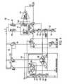
- a bandgap voltage reference circuit 100illustratively but not necessarily in the form of a Brokaw cell, which comprises a pair of transistors Q 1 and Q 2 supplied with positive and negative supply voltages V+, V ⁇ , with the emitters of transistors Q 1 and Q 2 interconnected through a resistor 110 .
- Resistors 112 and 114are connected serially between resistor 110 and negative voltage reference V ⁇ . Coupled between the collectors of transistors Q 1 , Q 2 and positive voltage reference V+ are collector resistors R 4 and R 5 in series, respectively, with trim resistors 102 a , 102 b of a post package trim 102 .
- Taps of trim resistors 102 a , 102 bare coupled respectively to the non-inverting and inverting inputs of operational amplifier 118 , the output of which is connected to output node 120 of circuit 100 , which supplies the produced reference voltage, and to the bases of transistors Q 1 , Q 2 .
- the node 116 between resistors 110 and 112develops VPAT as a result of resistor 110 , to compensate for the negative temperature coefficient of the V BE voltage drop of transistor Q 2 , as implemented in the conventional Brokaw type cell.
- resistors 112 and 114are unified in the conventional cell, they are represented in circuit 100 in the form of separate resistors 112 , 114 , joined at node 122 in FIG. 4 .
- circuit 100will develop an uncorrected reference output waveform (other than in first order correction by the Brokaw cell architecture), referenced as trace 4 ( a ) in FIG. 6 .
- the parabolic shape of this waveformis enhanced visually for emphasis by expanded y-axis scaling. Without Brokaw first order correction, the temperature dependency of reference voltage value would be considerably more severe.
- Coupled between output node 120 and negative reference voltage V ⁇is an output voltage dividing resistor network 124 comprising, in series, resistors 126 , 128 and 130 .
- the purpose of the divider 124is to develop an output voltage higher than the bandgap voltage by adding another resistor in series with the output of operational amplifier 118 .
- FIGS. 4 and 5show a unity gain implementation.
- An additional purpose of divider 124is to develop voltage levels for the second order curvature correction circuit.
- the output of operational amplifier 118is also applied to the input of a self-bias network 132 comprising transistor Q 3 and emitter resistor 133 .
- Current through transistor Q 3is of a magnitude dependent on the output voltage at node 120 and the value of resistor 133 .
- This currentflows through input transistor 136 of current mirror 134 and replicated by transistors 138 , 140 to be applied as inputs to curvature correction circuit 142 .
- Resistor 133being fixed in value, the current applied to the correction circuit 142 tracks the output voltage of reference circuit 100 produced at node 120 .
- Transistors Q 1 -Q 3 in the illustrative embodimentare npn bipolar transistors. Other transistors in FIG. 4 are field effect transistors. Transistor type and polarity may be changed depending on circuit architecture implemented.
- Curvature correction circuit 142comprises a pair of differential transistor pairs 144 and 146 in series with mirror transistors 138 and 140 , respectively.
- the sources of transistors 144 a and 144 b of pair 144are commonly connected to the drain of mirror transistor 138 .
- the sources of transistors 146 a and 146 b of pair 146are connected to the drain of mirror transistor 140 .
- Transistors 136 , 138 and 140 in this exampleare equally sized, whereby the mirrored currents produced by transistors 138 and 140 are equal to each other and to the current through transistor 136 ; this could be varied to accommodate particular tuning of curvature correction circuit 142 .
- Each transistor differential pair 144 , 146which may be a Gilbert cell as depicted in this example, is an analog multiplier which multiplies together signals applied to the respective transistor gates.
- the outputs of the two differential pairsare hard wire summed to supply a correction current to the Brokaw cell, in this example at the junction 122 between resistors 112 and 114 .
- the gates of transistors 144 b and 146 bare connected to the Brokaw cell at node 116 between resistors 112 and 116 .
- One side of differential transistor pairs 144 and 146thus is responsive to the PTAT voltage developed in the Brokaw cell.
- the level of voltage applied to gate 144 ais less than that applied to the gate of transistor 146 a in amount based upon the values of resistors 126 , 128 and 130 , tuned to desired curvature correction characteristics.
- Curvature correction circuit 142reduces temperature error in the Brokaw cell.
- Differential pairs 144 and 146are tuned to provide an appropriate current component at given temperatures.
- Each of the differential pairs 144 and 146generates a component of correction current I correct .
- I correctFor example, consider differential pair 146 which contributes a first component of correction current I correct .
- the gate voltage of transistor 146 bis less than the gate voltage of transistor 146 a .
- Most of the current from mirror transistor 140is diverted through transistor 146 a to contribute to I correct .
- the correction currentis approximately proportional to the current through current mirror transistor 140 .
- the gate voltage of transistor 146 beventually will match that of transistor 146 a . Now, only half of the current through transistor 140 passes through transistor 146 b to contribute to correction current I correct . This temperature is often referred to as the “crossing point” of the correction circuit. At very high temperatures, the gate of transistor 146 b is higher in voltage than the gate of transistor 146 a , and very little of the current through mirror transistor 140 contributes to correction current I correct .
- each differential pairBy adjusting the crossing point of each differential pair, it is possible to change the current contribution profile of each pair until the sum of the contributions results in the correction current that generally reduces temperature error in the output voltage of the Brokaw cell.
- the crossing points in practicemay be set by adjusting the relative sizes of resistors 126 , 128 and 130 . Similar description applies to differential pair 144 , whose gate inputs are obtained from node 116 of the Brokaw cell and the constant voltage at the node 129 between output divider resistors 128 and 130 .
- the currents produced by differential pairs 144 and 146are hard wire summed to achieve correction current I correct .
- Self-bias network 132develops curvature correction circuit input currents that track current in the bandgap reference, and hence supply input current to the curvature correction circuit 142 of magnitude that matches automatically to devices and materials that form the bandgap reference. For example, if the sheet resistance of the resistors forming the bandgap reference is low, the current through the bandgap core commensurately is high, creating a higher correction current and thus tracking the behavior of the core.
- the sum of the values of cell resistors 112 and 114nominally is equal to the value of resistor 116 .
- the transistor emitter areastend to deform, creating post package shift that affects the absolute voltage and drift of the bandgap core. This can be compensated by altering the values of those resistors 112 and 114 . Trimming the sizes of resistors 112 and 114 would require addition of field effect transistors in the emitter circuit the cell.
- post package trim 102is located in the collector circuits of transistors Q 1 and Q 2 , in accord with an aspect of the teachings herein, field effect transistors in the emitter circuit are unnecessary.
- Trimmay be implemented by arranging trim resistors 102 a and 102 b in the form of tapped resistors in which tap selection is carried out using fusing. As the tap on one of the trim resistors moves up, the tap on the other resistor moves down so that tap resistor values of the two resistors adjust oppositely.
- the sizes of tap resistors 102 a , 102 bdetermine trim range, and the number of taps determines trim resolution. Other trim arrangements could be used.
- Implementing trim in the collector circuit of the Brokaw transistorsenables products to be tested and measured to confirm conformance to a prescribed reference circuit specification.
- FIG. 5another embodiment includes a third order curvature correction circuit 300 that contributes a third order correction current to I correct .
- Circuit 300comprises first and second differential pairs 302 and 304 that correspond to differential pairs 144 and 146 of FIG. 4 .
- the input current to the third order curvature correction circuit 300is mirrored from the drain current of transistor 144 a , 144 b .
- the drain current of transistor 144 a in FIG. 4flows directly to V ⁇ , and in a sense is “discarded,” the counterpart current in FIG. 5 flows to V ⁇ through input transistor 306 of mirror 308 .
- Mirror 308in turn replicates the current to transistor pairs 302 and 304 .
- the third order curvature correction circuit 300is of structure and function that are identical to those of second order curvature correction circuit 142 .
- transistors 310 and 312are added to the circuit of FIG. 4 , of which in the example transistor 310 is a bipolar pnp transistor and transistor 312 is a field effect transistor whose current is controlled by self-bias network 132 .
- Transistors 310 and 312comprise a low drift voltage-to-current converter to develop a temperature independent current to bias second order curvature correction circuit 142 .
- the purpose of these transistorsis to use the V BE of transistor 310 to compensate for V BE change with temperature in transistor Q 3 thereby to reduce tilt in current profile that tends to arise especially with respect to third order correction in the embodiment of FIG. 5 .
- the voltage-to-current converterpreferably is implemented using the same type of resistor material as the bandgap core circuit. Since the V BE voltages of transistors Q 3 and Q 4 tend not to track well with process variations, a conventional voltage-to-current converter can be used.
- FIG. 6shows three plots that illustrate first, second and third order correction, together with respective improvement in performance using the principles taught herein.
- the second and third order correction currentsare shown in FIGS. 7( a ) and 7 ( b ). It is apparent from these drawings that correction current takes on the “inverse” shape of the previously uncorrected bandgap temperature response.
- bandgap cores of the type described in the Price '664 patenthave numerous advantages over bandgap cores of the type described in the Price '664 patent.
- the correction current in the '664 patentrequires some bandgap multiple as an output (i.e., the bandgap requires gain)
- the currently described bandgaprequires no gain (although gain could be implemented, if desired).
- correction currentis developed across a feedback resistor requiring that the feedback resistor match the bandgap core resistors.
- the feedback resistorwill have to match the output voltage divider string to precisely set gain.
- all the resistors in the '664 circuitneed critical matching to each other.
- the bandgap core resistorsneed not match the output feedback resistors.
- the inventionis capable of use in various other combinations and environments and is capable of changes or modifications within the scope of the inventive concept as expressed herein.
- certain transistors in the illustrative embodimentsare bipolar transistors, and others field effect transistors of polarities shown, the circuit could be reconfigured to accommodate other transistor types and polarities.
- the relative sizes of the differential and mirror transistorsmay vary.
- the bandgap cellmay have gain, and different order correction currents may be injected into taps of the bandgap resistor string other than as shown.
- the inputs to the differential transistor pairsmay be connected to different resistor string taps.
- the bandgap coremay be other than a Brokaw type cell, as has been illustrated by way of example.
Landscapes
- Engineering & Computer Science (AREA)
- Microelectronics & Electronic Packaging (AREA)
- Physics & Mathematics (AREA)
- Power Engineering (AREA)
- Nonlinear Science (AREA)
- Electromagnetism (AREA)
- General Physics & Mathematics (AREA)
- Radar, Positioning & Navigation (AREA)
- Automation & Control Theory (AREA)
- Control Of Electrical Variables (AREA)
Abstract
Description
Claims (19)
Priority Applications (1)
| Application Number | Priority Date | Filing Date | Title |
|---|---|---|---|
| US11/377,451US7420359B1 (en) | 2006-03-17 | 2006-03-17 | Bandgap curvature correction and post-package trim implemented therewith |
Applications Claiming Priority (1)
| Application Number | Priority Date | Filing Date | Title |
|---|---|---|---|
| US11/377,451US7420359B1 (en) | 2006-03-17 | 2006-03-17 | Bandgap curvature correction and post-package trim implemented therewith |
Publications (1)
| Publication Number | Publication Date |
|---|---|
| US7420359B1true US7420359B1 (en) | 2008-09-02 |
Family
ID=39718392
Family Applications (1)
| Application Number | Title | Priority Date | Filing Date |
|---|---|---|---|
| US11/377,451Active2026-08-27US7420359B1 (en) | 2006-03-17 | 2006-03-17 | Bandgap curvature correction and post-package trim implemented therewith |
Country Status (1)
| Country | Link |
|---|---|
| US (1) | US7420359B1 (en) |
Cited By (31)
| Publication number | Priority date | Publication date | Assignee | Title |
|---|---|---|---|---|
| US20080315855A1 (en)* | 2007-06-19 | 2008-12-25 | Sean Xiao | Low power bandgap voltage reference circuit having multiple reference voltages with high power supply rejection ratio |
| US20110084681A1 (en)* | 2009-10-08 | 2011-04-14 | Intersil Americas Inc. | Circuits and methods to produce a vptat and/or a bandgap voltage with low-glitch preconditioning |
| US20110127987A1 (en)* | 2009-11-30 | 2011-06-02 | Intersil Americas Inc. | Circuits and methods to produce a bandgap voltage with low-drift |
| US20110127988A1 (en)* | 2009-12-02 | 2011-06-02 | Intersil Americas Inc. | Rotating gain resistors to produce a bandgap voltage with low-drift |
| US20110227636A1 (en)* | 2010-03-19 | 2011-09-22 | Fujitsu Semiconductor Limited | Reference voltage circuit and semiconductor integrated circuit |
| WO2012109805A1 (en)* | 2011-02-18 | 2012-08-23 | 电子科技大学 | Temperature self-adaption bandgap reference circuit |
| CN102809979A (en)* | 2012-07-13 | 2012-12-05 | 电子科技大学 | A third-order compensated bandgap reference voltage source |
| CN103116380A (en)* | 2011-11-16 | 2013-05-22 | 瑞萨电子株式会社 | Bandgap reference circuit and power supply circuit |
| US8493130B2 (en) | 2011-08-02 | 2013-07-23 | Renesas Electronics Corporation | Reference voltage generating circuit |
| JP2013149197A (en)* | 2012-01-23 | 2013-08-01 | Renesas Electronics Corp | Reference voltage generation circuit |
| CN103294099A (en)* | 2013-05-17 | 2013-09-11 | 电子科技大学 | Second-order curvature temperature-compensation circuit for band-gap reference |
| US20130328615A1 (en)* | 2012-06-07 | 2013-12-12 | Renesas Electronics Corporation | Semiconductor dev ice having voltage generation circuit |
| US8638084B1 (en)* | 2010-10-22 | 2014-01-28 | Xilinx, Inc. | Bandgap bias circuit compenastion using a current density range and resistive loads |
| JP2014063431A (en)* | 2012-09-24 | 2014-04-10 | Toshiba Corp | Reference voltage generator circuit |
| US8791683B1 (en) | 2011-02-28 | 2014-07-29 | Linear Technology Corporation | Voltage-mode band-gap reference circuit with temperature drift and output voltage trims |
| US20150084686A1 (en)* | 2013-09-24 | 2015-03-26 | Semiconductor Components Industries, Llc | Compensated voltage reference generation circuit and method |
| US9069369B1 (en)* | 2012-03-30 | 2015-06-30 | Altera Corporation | Voltage regulator and a method to operate the voltage regulator |
| US9098098B2 (en) | 2012-11-01 | 2015-08-04 | Invensense, Inc. | Curvature-corrected bandgap reference |
| US9864389B1 (en)* | 2016-11-10 | 2018-01-09 | Analog Devices Global | Temperature compensated reference voltage circuit |
| CN109407747A (en)* | 2018-12-19 | 2019-03-01 | 佛山臻智微芯科技有限公司 | A kind of band-gap reference circuit of the high PSRR of second-order temperature compensation |
| JP2019133569A (en)* | 2018-02-02 | 2019-08-08 | 株式会社デンソー | Correction current output circuit and reference voltage circuit with correction function |
| TWI727435B (en)* | 2018-09-28 | 2021-05-11 | 台灣積體電路製造股份有限公司 | Thermal sensor and method of temperature measurement |
| CN113885634A (en)* | 2021-11-02 | 2022-01-04 | 苏州华矽共创信息技术合伙企业(有限合伙) | Band-gap reference voltage source suitable for low-current gain type NPN triode |
| US11329612B2 (en) | 2019-11-27 | 2022-05-10 | Analog Devices International Unlimited Company | Interface cell for circuit adjustment |
| WO2022221180A1 (en)* | 2021-04-12 | 2022-10-20 | Texas Instruments Incorporated | Compensation of thermally induced voltage errors |
| US11782469B1 (en)* | 2022-04-11 | 2023-10-10 | Richtek Technology Corporation | Reference signal generator having high order temperature compensation |
| US20230324941A1 (en)* | 2021-10-18 | 2023-10-12 | Texas Instruments Incorporated | Bandgap current reference |
| US11789482B2 (en) | 2021-03-26 | 2023-10-17 | Samsung Electronics Co., Ltd. | Bandgap reference circuit including resistivity temperature coefficient cancellation circuit, and oscillator circuit including the bandgap reference circuit |
| US11876490B2 (en) | 2021-04-12 | 2024-01-16 | Texas Instruments Incorporated | Compensation of thermally induced voltage errors |
| US20240393819A1 (en)* | 2023-05-25 | 2024-11-28 | Silicon Laboratories Inc. | Voltage and current reference circuits |
| US20250155908A1 (en)* | 2023-11-15 | 2025-05-15 | Analog Devices, Inc. | Low supply headroom bandgap voltage reference |
Citations (12)
| Publication number | Priority date | Publication date | Assignee | Title |
|---|---|---|---|---|
| US3887863A (en) | 1973-11-28 | 1975-06-03 | Analog Devices Inc | Solid-state regulated voltage supply |
| US4795961A (en)* | 1987-06-10 | 1989-01-03 | Unitrode Corporation | Low-noise voltage reference |
| US4939442A (en)* | 1989-03-30 | 1990-07-03 | Texas Instruments Incorporated | Bandgap voltage reference and method with further temperature correction |
| US5391980A (en)* | 1993-06-16 | 1995-02-21 | Texas Instruments Incorporated | Second order low temperature coefficient bandgap voltage supply |
| US5619163A (en)* | 1995-03-17 | 1997-04-08 | Maxim Integrated Products, Inc. | Bandgap voltage reference and method for providing same |
| US5767664A (en) | 1996-10-29 | 1998-06-16 | Unitrode Corporation | Bandgap voltage reference based temperature compensation circuit |
| US6342781B1 (en)* | 2001-04-13 | 2002-01-29 | Ami Semiconductor, Inc. | Circuits and methods for providing a bandgap voltage reference using composite resistors |
| US6346848B1 (en)* | 2000-06-29 | 2002-02-12 | International Business Machines Corporation | Apparatus and method for generating current linearly dependent on temperature |
| US6462526B1 (en)* | 2001-08-01 | 2002-10-08 | Maxim Integrated Products, Inc. | Low noise bandgap voltage reference circuit |
| US6642699B1 (en) | 2002-04-29 | 2003-11-04 | Ami Semiconductor, Inc. | Bandgap voltage reference using differential pairs to perform temperature curvature compensation |
| US6891358B2 (en) | 2002-12-27 | 2005-05-10 | Analog Devices, Inc. | Bandgap voltage reference circuit with high power supply rejection ratio (PSRR) and curvature correction |
| US6906581B2 (en)* | 2002-04-30 | 2005-06-14 | Realtek Semiconductor Corp. | Fast start-up low-voltage bandgap voltage reference circuit |
- 2006
- 2006-03-17USUS11/377,451patent/US7420359B1/enactiveActive
Patent Citations (12)
| Publication number | Priority date | Publication date | Assignee | Title |
|---|---|---|---|---|
| US3887863A (en) | 1973-11-28 | 1975-06-03 | Analog Devices Inc | Solid-state regulated voltage supply |
| US4795961A (en)* | 1987-06-10 | 1989-01-03 | Unitrode Corporation | Low-noise voltage reference |
| US4939442A (en)* | 1989-03-30 | 1990-07-03 | Texas Instruments Incorporated | Bandgap voltage reference and method with further temperature correction |
| US5391980A (en)* | 1993-06-16 | 1995-02-21 | Texas Instruments Incorporated | Second order low temperature coefficient bandgap voltage supply |
| US5619163A (en)* | 1995-03-17 | 1997-04-08 | Maxim Integrated Products, Inc. | Bandgap voltage reference and method for providing same |
| US5767664A (en) | 1996-10-29 | 1998-06-16 | Unitrode Corporation | Bandgap voltage reference based temperature compensation circuit |
| US6346848B1 (en)* | 2000-06-29 | 2002-02-12 | International Business Machines Corporation | Apparatus and method for generating current linearly dependent on temperature |
| US6342781B1 (en)* | 2001-04-13 | 2002-01-29 | Ami Semiconductor, Inc. | Circuits and methods for providing a bandgap voltage reference using composite resistors |
| US6462526B1 (en)* | 2001-08-01 | 2002-10-08 | Maxim Integrated Products, Inc. | Low noise bandgap voltage reference circuit |
| US6642699B1 (en) | 2002-04-29 | 2003-11-04 | Ami Semiconductor, Inc. | Bandgap voltage reference using differential pairs to perform temperature curvature compensation |
| US6906581B2 (en)* | 2002-04-30 | 2005-06-14 | Realtek Semiconductor Corp. | Fast start-up low-voltage bandgap voltage reference circuit |
| US6891358B2 (en) | 2002-12-27 | 2005-05-10 | Analog Devices, Inc. | Bandgap voltage reference circuit with high power supply rejection ratio (PSRR) and curvature correction |
Non-Patent Citations (1)
| Title |
|---|
| Gupta et al., "Predicting and Designing for the Impact of Process Variations and Mismatch on the Trim Range and Yield of Bandgap References", GT Analog and Power IC Design Lab, Georgia Institute of Technology, 6 pages. |
Cited By (55)
| Publication number | Priority date | Publication date | Assignee | Title |
|---|---|---|---|---|
| US20080315855A1 (en)* | 2007-06-19 | 2008-12-25 | Sean Xiao | Low power bandgap voltage reference circuit having multiple reference voltages with high power supply rejection ratio |
| US7656145B2 (en)* | 2007-06-19 | 2010-02-02 | O2Micro International Limited | Low power bandgap voltage reference circuit having multiple reference voltages with high power supply rejection ratio |
| US20110084681A1 (en)* | 2009-10-08 | 2011-04-14 | Intersil Americas Inc. | Circuits and methods to produce a vptat and/or a bandgap voltage with low-glitch preconditioning |
| US8330445B2 (en) | 2009-10-08 | 2012-12-11 | Intersil Americas Inc. | Circuits and methods to produce a VPTAT and/or a bandgap voltage with low-glitch preconditioning |
| US20110127987A1 (en)* | 2009-11-30 | 2011-06-02 | Intersil Americas Inc. | Circuits and methods to produce a bandgap voltage with low-drift |
| US8446140B2 (en) | 2009-11-30 | 2013-05-21 | Intersil Americas Inc. | Circuits and methods to produce a bandgap voltage with low-drift |
| US8278905B2 (en)* | 2009-12-02 | 2012-10-02 | Intersil Americas Inc. | Rotating gain resistors to produce a bandgap voltage with low-drift |
| US20110127988A1 (en)* | 2009-12-02 | 2011-06-02 | Intersil Americas Inc. | Rotating gain resistors to produce a bandgap voltage with low-drift |
| US20110227636A1 (en)* | 2010-03-19 | 2011-09-22 | Fujitsu Semiconductor Limited | Reference voltage circuit and semiconductor integrated circuit |
| US8786358B2 (en)* | 2010-03-19 | 2014-07-22 | Spansion Llc | Reference voltage circuit and semiconductor integrated circuit |
| US8638084B1 (en)* | 2010-10-22 | 2014-01-28 | Xilinx, Inc. | Bandgap bias circuit compenastion using a current density range and resistive loads |
| WO2012109805A1 (en)* | 2011-02-18 | 2012-08-23 | 电子科技大学 | Temperature self-adaption bandgap reference circuit |
| US8907650B2 (en) | 2011-02-18 | 2014-12-09 | University Of Electronic Science And Technology Of China | Temperature adaptive bandgap reference circuit |
| US8791683B1 (en) | 2011-02-28 | 2014-07-29 | Linear Technology Corporation | Voltage-mode band-gap reference circuit with temperature drift and output voltage trims |
| US8493130B2 (en) | 2011-08-02 | 2013-07-23 | Renesas Electronics Corporation | Reference voltage generating circuit |
| US10209731B2 (en) | 2011-11-16 | 2019-02-19 | Renesas Electronics Corporation | Bandgap reference circuit and power supply circuit |
| EP2595028A2 (en) | 2011-11-16 | 2013-05-22 | Renesas Electronics Corporation | Bandgap reference circuit and power supply circuit |
| US9367077B2 (en) | 2011-11-16 | 2016-06-14 | Renesas Electronics Corporation | Bandgap reference circuit and power supply circuit |
| US9891647B2 (en) | 2011-11-16 | 2018-02-13 | Renesas Electronics Corporation | Bandgap reference circuit and power supply circuit |
| CN103116380B (en)* | 2011-11-16 | 2016-03-16 | 瑞萨电子株式会社 | Band-gap reference circuit and power circuit |
| CN103116380A (en)* | 2011-11-16 | 2013-05-22 | 瑞萨电子株式会社 | Bandgap reference circuit and power supply circuit |
| US9335778B2 (en) | 2012-01-23 | 2016-05-10 | Renesas Electronics Corporation | Reference voltage generating circuit |
| US8988137B2 (en) | 2012-01-23 | 2015-03-24 | Renesas Electronics Corporation | Reference voltage generating circuit |
| JP2013149197A (en)* | 2012-01-23 | 2013-08-01 | Renesas Electronics Corp | Reference voltage generation circuit |
| US9069369B1 (en)* | 2012-03-30 | 2015-06-30 | Altera Corporation | Voltage regulator and a method to operate the voltage regulator |
| CN103488234A (en)* | 2012-06-07 | 2014-01-01 | 瑞萨电子株式会社 | Semiconductor device with voltage generating circuit |
| US8866539B2 (en)* | 2012-06-07 | 2014-10-21 | Renesas Electronics Corporation | Semiconductor device having voltage generation circuit |
| US10152078B2 (en) | 2012-06-07 | 2018-12-11 | Renesas Electronics Corporation | Semiconductor device having voltage generation circuit |
| TWI584100B (en)* | 2012-06-07 | 2017-05-21 | 瑞薩電子股份有限公司 | Semiconductor device with voltage generating circuit |
| CN103488234B (en)* | 2012-06-07 | 2017-03-22 | 瑞萨电子株式会社 | Semiconductor device with voltage generating circuit |
| US20130328615A1 (en)* | 2012-06-07 | 2013-12-12 | Renesas Electronics Corporation | Semiconductor dev ice having voltage generation circuit |
| US9436195B2 (en) | 2012-06-07 | 2016-09-06 | Renesas Electronics Corporation | Semiconductor device having voltage generation circuit |
| CN102809979A (en)* | 2012-07-13 | 2012-12-05 | 电子科技大学 | A third-order compensated bandgap reference voltage source |
| CN102809979B (en)* | 2012-07-13 | 2014-07-02 | 电子科技大学 | Third-order compensation band-gap reference voltage source |
| JP2014063431A (en)* | 2012-09-24 | 2014-04-10 | Toshiba Corp | Reference voltage generator circuit |
| US9098098B2 (en) | 2012-11-01 | 2015-08-04 | Invensense, Inc. | Curvature-corrected bandgap reference |
| CN103294099A (en)* | 2013-05-17 | 2013-09-11 | 电子科技大学 | Second-order curvature temperature-compensation circuit for band-gap reference |
| CN103294099B (en)* | 2013-05-17 | 2015-04-15 | 电子科技大学 | Second-order curvature temperature-compensation circuit for band-gap reference |
| US9568928B2 (en)* | 2013-09-24 | 2017-02-14 | Semiconductor Components Indutries, Llc | Compensated voltage reference generation circuit and method |
| US20150084686A1 (en)* | 2013-09-24 | 2015-03-26 | Semiconductor Components Industries, Llc | Compensated voltage reference generation circuit and method |
| US9864389B1 (en)* | 2016-11-10 | 2018-01-09 | Analog Devices Global | Temperature compensated reference voltage circuit |
| JP2019133569A (en)* | 2018-02-02 | 2019-08-08 | 株式会社デンソー | Correction current output circuit and reference voltage circuit with correction function |
| WO2019150744A1 (en)* | 2018-02-02 | 2019-08-08 | 株式会社デンソー | Correction current output circuit and reference voltage circuit with correction function |
| US11181937B2 (en)* | 2018-02-02 | 2021-11-23 | Denso Corporation | Correction current output circuit and reference voltage circuit with correction function |
| TWI727435B (en)* | 2018-09-28 | 2021-05-11 | 台灣積體電路製造股份有限公司 | Thermal sensor and method of temperature measurement |
| CN109407747A (en)* | 2018-12-19 | 2019-03-01 | 佛山臻智微芯科技有限公司 | A kind of band-gap reference circuit of the high PSRR of second-order temperature compensation |
| US11329612B2 (en) | 2019-11-27 | 2022-05-10 | Analog Devices International Unlimited Company | Interface cell for circuit adjustment |
| US11789482B2 (en) | 2021-03-26 | 2023-10-17 | Samsung Electronics Co., Ltd. | Bandgap reference circuit including resistivity temperature coefficient cancellation circuit, and oscillator circuit including the bandgap reference circuit |
| WO2022221180A1 (en)* | 2021-04-12 | 2022-10-20 | Texas Instruments Incorporated | Compensation of thermally induced voltage errors |
| US11876490B2 (en) | 2021-04-12 | 2024-01-16 | Texas Instruments Incorporated | Compensation of thermally induced voltage errors |
| US20230324941A1 (en)* | 2021-10-18 | 2023-10-12 | Texas Instruments Incorporated | Bandgap current reference |
| CN113885634A (en)* | 2021-11-02 | 2022-01-04 | 苏州华矽共创信息技术合伙企业(有限合伙) | Band-gap reference voltage source suitable for low-current gain type NPN triode |
| US11782469B1 (en)* | 2022-04-11 | 2023-10-10 | Richtek Technology Corporation | Reference signal generator having high order temperature compensation |
| US20240393819A1 (en)* | 2023-05-25 | 2024-11-28 | Silicon Laboratories Inc. | Voltage and current reference circuits |
| US20250155908A1 (en)* | 2023-11-15 | 2025-05-15 | Analog Devices, Inc. | Low supply headroom bandgap voltage reference |
Similar Documents
| Publication | Publication Date | Title |
|---|---|---|
| US7420359B1 (en) | Bandgap curvature correction and post-package trim implemented therewith | |
| US6642699B1 (en) | Bandgap voltage reference using differential pairs to perform temperature curvature compensation | |
| US8102201B2 (en) | Reference circuit and method for providing a reference | |
| US7576598B2 (en) | Bandgap voltage reference and method for providing same | |
| JP3647468B2 (en) | Dual source for constant current and PTAT current | |
| US6828847B1 (en) | Bandgap voltage reference circuit and method for producing a temperature curvature corrected voltage reference | |
| US7253597B2 (en) | Curvature corrected bandgap reference circuit and method | |
| US10890935B2 (en) | Bandgap current architecture optimized for size and accuracy | |
| US10671109B2 (en) | Scalable low output impedance bandgap reference with current drive capability and high-order temperature curvature compensation | |
| US7541862B2 (en) | Reference voltage generating circuit | |
| US8212606B2 (en) | Apparatus and method for offset drift trimming | |
| US20050242799A1 (en) | Method and circuit for generating a higher order compensated bandgap voltage | |
| US6426669B1 (en) | Low voltage bandgap reference circuit | |
| US5245273A (en) | Bandgap voltage reference circuit | |
| US7323857B2 (en) | Current source with adjustable temperature coefficient | |
| US8159206B2 (en) | Voltage reference circuit based on 3-transistor bandgap cell | |
| US20060001413A1 (en) | Proportional to absolute temperature voltage circuit | |
| US8461914B2 (en) | Reference signal generating circuit | |
| US20150331439A1 (en) | Electronic Device and Method for Generating a Curvature Compensated Bandgap Reference Voltage | |
| KR20120080567A (en) | Compensated bandgap | |
| US10416702B2 (en) | Bandgap reference circuit, corresponding device and method | |
| US11480989B2 (en) | High accuracy zener based voltage reference circuit | |
| US20060006858A1 (en) | Method and apparatus for generating n-order compensated temperature independent reference voltage | |
| JPH0784659A (en) | Curvature correcting circuit for voltage reference | |
| US6509783B2 (en) | Generation of a voltage proportional to temperature with a negative variation |
Legal Events
| Date | Code | Title | Description |
|---|---|---|---|
| AS | Assignment | Owner name:LINEAR TECHNOLOGY CORPORATION, CALIFORNIA Free format text:ASSIGNMENT OF ASSIGNORS INTEREST;ASSIGNORS:ANDERSON, MICHAEL;GARDNER, ANDREW;CHIACCHIA, ROBERT;REEL/FRAME:017699/0753 Effective date:20050315 | |
| STCF | Information on status: patent grant | Free format text:PATENTED CASE | |
| FPAY | Fee payment | Year of fee payment:4 | |
| FPAY | Fee payment | Year of fee payment:8 | |
| MAFP | Maintenance fee payment | Free format text:PAYMENT OF MAINTENANCE FEE, 12TH YEAR, LARGE ENTITY (ORIGINAL EVENT CODE: M1553); ENTITY STATUS OF PATENT OWNER: LARGE ENTITY Year of fee payment:12 | |
| AS | Assignment | Owner name:ANALOG DEVICES INTERNATIONAL UNLIMITED COMPANY, IRELAND Free format text:CHANGE OF NAME;ASSIGNOR:LINEAR TECHNOLOGY LLC;REEL/FRAME:057423/0001 Effective date:20181105 Owner name:LINEAR TECHNOLOGY LLC, CALIFORNIA Free format text:CHANGE OF NAME;ASSIGNOR:LINEAR TECHNOLOGY CORPORATION;REEL/FRAME:057421/0543 Effective date:20170502 |