US7420248B2 - Programmable random logic arrays using PN isolation - Google Patents
Programmable random logic arrays using PN isolationDownload PDFInfo
- Publication number
- US7420248B2 US7420248B2US11/211,813US21181305AUS7420248B2US 7420248 B2US7420248 B2US 7420248B2US 21181305 AUS21181305 AUS 21181305AUS 7420248 B2US7420248 B2US 7420248B2
- Authority
- US
- United States
- Prior art keywords
- regions
- region
- contacts
- logic device
- type
- Prior art date
- Legal status (The legal status is an assumption and is not a legal conclusion. Google has not performed a legal analysis and makes no representation as to the accuracy of the status listed.)
- Active, expires
Links
- 238000002955isolationMethods0.000titledescription4
- 238000003491arrayMethods0.000titledescription2
- 239000004065semiconductorSubstances0.000claimsabstractdescription28
- 239000000758substrateSubstances0.000claimsabstractdescription13
- 150000002500ionsChemical class0.000claims2
- 238000000034methodMethods0.000abstractdescription17
- 238000004519manufacturing processMethods0.000description9
- 239000002019doping agentSubstances0.000description8
- 230000003247decreasing effectEffects0.000description4
- 238000002513implantationMethods0.000description4
- 235000012431wafersNutrition0.000description4
- XUIMIQQOPSSXEZ-UHFFFAOYSA-NSiliconChemical compound[Si]XUIMIQQOPSSXEZ-UHFFFAOYSA-N0.000description3
- 239000000463materialSubstances0.000description3
- 229910052710siliconInorganic materials0.000description3
- 239000010703siliconSubstances0.000description3
- -1arsenic ionsChemical class0.000description2
- 230000015572biosynthetic processEffects0.000description2
- 229910052751metalInorganic materials0.000description2
- 239000002184metalSubstances0.000description2
- 238000012986modificationMethods0.000description2
- 230000004048modificationEffects0.000description2
- 230000003071parasitic effectEffects0.000description2
- 238000000059patterningMethods0.000description2
- 239000002243precursorSubstances0.000description2
- 229910052785arsenicInorganic materials0.000description1
- 229910052796boronInorganic materials0.000description1
- 238000010276constructionMethods0.000description1
- BHEPBYXIRTUNPN-UHFFFAOYSA-Nhydridophosphorus(.) (triplet)Chemical compound[PH]BHEPBYXIRTUNPN-UHFFFAOYSA-N0.000description1
- 239000007943implantSubstances0.000description1
- 238000005468ion implantationMethods0.000description1
- 230000000873masking effectEffects0.000description1
- 238000001465metallisationMethods0.000description1
Images


Classifications
- H—ELECTRICITY
- H10—SEMICONDUCTOR DEVICES; ELECTRIC SOLID-STATE DEVICES NOT OTHERWISE PROVIDED FOR
- H10D—INORGANIC ELECTRIC SEMICONDUCTOR DEVICES
- H10D84/00—Integrated devices formed in or on semiconductor substrates that comprise only semiconducting layers, e.g. on Si wafers or on GaAs-on-Si wafers
- H10D84/90—Masterslice integrated circuits
- H—ELECTRICITY
- H10—SEMICONDUCTOR DEVICES; ELECTRIC SOLID-STATE DEVICES NOT OTHERWISE PROVIDED FOR
- H10D—INORGANIC ELECTRIC SEMICONDUCTOR DEVICES
- H10D84/00—Integrated devices formed in or on semiconductor substrates that comprise only semiconducting layers, e.g. on Si wafers or on GaAs-on-Si wafers
- H—ELECTRICITY
- H10—SEMICONDUCTOR DEVICES; ELECTRIC SOLID-STATE DEVICES NOT OTHERWISE PROVIDED FOR
- H10D—INORGANIC ELECTRIC SEMICONDUCTOR DEVICES
- H10D86/00—Integrated devices formed in or on insulating or conducting substrates, e.g. formed in silicon-on-insulator [SOI] substrates or on stainless steel or glass substrates
- H10D86/01—Manufacture or treatment
- H—ELECTRICITY
- H10—SEMICONDUCTOR DEVICES; ELECTRIC SOLID-STATE DEVICES NOT OTHERWISE PROVIDED FOR
- H10D—INORGANIC ELECTRIC SEMICONDUCTOR DEVICES
- H10D86/00—Integrated devices formed in or on insulating or conducting substrates, e.g. formed in silicon-on-insulator [SOI] substrates or on stainless steel or glass substrates
- H10D86/201—Integrated devices formed in or on insulating or conducting substrates, e.g. formed in silicon-on-insulator [SOI] substrates or on stainless steel or glass substrates the substrates comprising an insulating layer on a semiconductor body, e.g. SOI
- H—ELECTRICITY
- H10—SEMICONDUCTOR DEVICES; ELECTRIC SOLID-STATE DEVICES NOT OTHERWISE PROVIDED FOR
- H10D—INORGANIC ELECTRIC SEMICONDUCTOR DEVICES
- H10D89/00—Aspects of integrated devices not covered by groups H10D84/00 - H10D88/00
- H10D89/10—Integrated device layouts
Definitions
- This inventiongenerally relates to integrated circuits. More specifically, the invention relates to random logic integrated circuit devices, and to methods for making such circuits.
- Integrated circuitsare an essential part of digital systems, such as computers.
- One challenge to the manufacturers of such circuitsis to provide each customer with a circuit that is or can be tailored to the specific needs of that customer.
- One wayis to provide circuits that are programmable or have random logic.
- Logiccan be designed and fixed, as in a gate array (GA) device, so that earlier, or “front end” (FE), process steps used in the manufacture of the circuits are quite generic, in particular, with respect to implantation and contact.
- FEfront end
- BEback end
- logiccan be re-programmed, as in field programmable gate arrays (FPGAs).
- FPGAsfield programmable gate arrays
- the logiccan be defined real-time, yielding a dynamically reconfigurable/random logic device.
- An object of this inventionis to improve programmable random logic array devices and methods for making such devices.
- Another object of the present inventionis to use PN isolation in a programmable random logic array.
- a further object of the inventionis to provide an ordered array of spaced apart PN junctions to form a programmable device array.
- the devicecomprises a substrate, and a semiconductor layer above the substrate. That semiconductor layer, in turn, includes a first region of a first semiconductor type, an array of spaced apart second regions of a second semiconductor type, and a plurality of space-charge regions. Each of the space charge regions extends around a respective one of the second regions and separates that one of the second regions from the first region of the semiconductor layer.
- the programmable, random, logic device arrayfurther comprises first and second sets of contacts.
- Each of the first set of contactsis above and in electrical contact with a respective one area of said first region of the semiconductor layer, and each of the second set of contacts is above and in electrical contact with a respective one of the second regions.
- the electrical contactsfacilitate connecting together said areas of the first region and the second regions in various, programmable ways.
- front-end processese.g., implantation, active devices
- front-end processesare generic or substantially generic, some are common between multiple devices, and devices can be defined into specific types by hard-wire (netlist).
- the active devices of the logic arraymay be PN junctions formed adjacent to one another so that their overlap regions form a space-charge region, thus isolating one device from another (in two or three dimensions).
- the front-end devicescan be formed over an entire wafer or regions of fixed or arbitrary geometry. Personalization may be accomplished or substantially accomplished via metal patterning in the back end processes. Further, preferably the invention is practiced on silicon on oxide (SOI) to reduce or minimize formation of parasitic transistor/path during circuit operation.
- SOIsilicon on oxide
- alternating P and N regionscan be utilized as isolation regions rather than directly as active devices. In this case, leakage from circuit blocks of dissimilar conductivity type does not affect circuits in neighboring regions.
- the present inventionmay be very useful as voltage thresholds (Vt's) are decreasing and critical geometries are decreasing, and, for these reasons, a simpler fabrication may be desirable as processing drives below ninety nanometers. Also, as channel thicknesses decrease, leakage may be mitigated to a point where the present invention is particularly valuable.
- the present inventionmay also reduce fabrication costs, since the fabrication process is simpler and supports generic (FE) precursors.
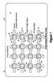
- FIG. 1is a top plane view illustrating a first embodiment of the invention.
- FIG. 2is a vertical cross-sectional view of the semiconductor structure of FIG. 1 .
- FIGS. 3 and 4show how elements of the array of FIG. 1 may be connected together to form a CMOS inverter.
- FIG. 5schematically illustrates the CMOS inverter formed by the array of FIG. 3 .
- FIG. 6illustrates a second embodiment of the invention.
- FIGS. 1 and 2show a semiconductor structure or wafer 10 comprising lower substrate 12 , upper semiconductor layer 14 , and a series of contacts, generally referenced at 16 ; and preferably, structure 10 further comprises oxide layer 20 between substrate 12 and layer 14 .
- Upper layer 14includes N-type region 22 , an array of P-type regions 24 , and a multitude of space-charge regions 26 .
- upper layer 14is comprised primarily of the N-type region 22
- the P-type regions 24are spaced apart in layer 14 , and each of those P-type regions is surrounded by a respective one of the space-charge regions. 26 .
- P-type regions 24are uniformly spaced apart in an orthogonal grid pattern, including parallel rows and parallel columns, with the rows perpendicular to the columns.
- Contacts 16are provided to help connect together various areas of the N-region and various P-regions of layer 14 . More particularly, a first set of the contacts are above and in electrical contact with specific areas of N-region 22 , and a second set of the contacts are above and in electrical contact with P regions 24 . With the arrangement shown in FIG. 1 , the first set of contacts are located on the rows and columns of the grid formed by the P-regions 24 . Further, four of these first set of contacts are uniformly spaced around each P-region—above, below, to the left, and to the right of that P-region.
- FIGS. 3 and 4show one way of connecting the P— and N-regions together to form an inverter.
- a P-region 24 a and an adjacent area 22 a of the N-regionare connected via an output connection 42 .
- the N-type area 22 b immediately to the left of P-region 24 a , and the P-region 24 b immediately to the right of N-type area 22 aare connected via an input connection 44 .
- P region 24 c to the left of N area 22 bis connected to ground, and the N area 22 c to the right of P-region 24 b is connected to a source voltage Vdd.
- oxide caps 46are deposited above the space charge regions 26 surrounding the P-regions in order to insulate those space charge regions from the connectors 42 and 44 .
- structure 10may be made in any suitable way.
- Lower substrate 12may be made of any suitable material, and for example, this substrate may be a bulk silicon substrate.
- Layer 20is preferably comprised of an oxide material, and is deposited on substrate 12 in any suitable way.
- Semiconductor layer 14may be formed by providing a suitable substrate, and then implanting N-type dopants to form N-region 22 , and implanting P-type dopants to form P-regions 24 .
- Contacts 16may be affixed in place on top of the N-region and P-regions.
- space-charge regions 26are preferably formed naturally as the result of implanting the P-type dopants in regions 24 .
- the P-type dopantsmigrate into N-region 22 and form an isolation interface between a P-region and the surrounding N-region.
- any suitable dopantsmay be used to form the N— and P-regions; and for example, the N-type dopants may be phosphorous or arsenic ions, and the P-type dopants may be boron ions. Also, any suitable masking technique or other suitable targeted ion implantation process may be used to implant the N and P type dopants in the desired areas of layer 14 .
- FIG. 6shows an alternate semiconductor layer 60 that can also be used in the practice of this invention.
- the P-regions 62separate the N-type material into a multitude of separate N-regions 64 .
- Semiconductor layer 60 of FIG. 6thus has alternating P and N regions, both in the horizontal direction and in the vertical direction, forming a checkerboard pattern.
- a first set of contacts, generally referenced at 66are affixed on the P-regions 62
- a second set of contactsare affixed on the N-regions 64 .
- FIG. 6also illustrates how the P and N regions of semiconductor layer 60 can be connected together to form an inverter, which is also represented by the schematic in FIG. 5 .
- a pair of adjacent P and N regionsare connected together via output connector 72
- the N region 64 b to the left of P region 62 ais connected to the P region 62 b to the right of N region 64 a via input connector 74 .
- P region 62 cwhich is to the left of N region 64 b
- N region 64 cwhich is to the right of P region 62 b
- VddVd
- front-end processese.g., implantation, active devices
- front-end processese.g., implantation, active devices
- the active devices of the logic arraymay be PN junctions formed adjacent to one another so that their overlap regions form a space-charge region, thus isolating one device from another (in two or three dimensions).
- the front end devicescan be formed over an entire wafer or regions of fixed or arbitrary geometry. Personalization may be accomplished or substantially accomplished via metal patterning in the back end processes. Further, preferably the invention is practiced on silicon on oxide (SOI) to reduce or minimize formation of parasitic transistor/path during circuit operation.
- SOIsilicon on oxide
- the present inventionmay be very useful as voltage thresholds (Vt's) are decreasing and critical geometries are decreasing, and, for these reasons, a simpler fabrication may be desirable as processing drives below ninety nanometers. Also, as channel thicknesses decrease, leakage may be mitigated to a point where the present invention is particularly valuable.
- the present inventionmay also reduce fabrication costs, since the fabrication process is simpler and supports generic (FE) precursors.
Landscapes
- Semiconductor Integrated Circuits (AREA)
- Metal-Oxide And Bipolar Metal-Oxide Semiconductor Integrated Circuits (AREA)
Abstract
Description
Claims (8)
Priority Applications (2)
| Application Number | Priority Date | Filing Date | Title |
|---|---|---|---|
| US11/211,813US7420248B2 (en) | 2005-08-25 | 2005-08-25 | Programmable random logic arrays using PN isolation |
| US11/871,484US7704802B2 (en) | 2005-08-25 | 2007-10-12 | Programmable random logic arrays using PN isolation |
Applications Claiming Priority (1)
| Application Number | Priority Date | Filing Date | Title |
|---|---|---|---|
| US11/211,813US7420248B2 (en) | 2005-08-25 | 2005-08-25 | Programmable random logic arrays using PN isolation |
Related Child Applications (1)
| Application Number | Title | Priority Date | Filing Date |
|---|---|---|---|
| US11/871,484DivisionUS7704802B2 (en) | 2005-08-25 | 2007-10-12 | Programmable random logic arrays using PN isolation |
Publications (2)
| Publication Number | Publication Date |
|---|---|
| US20070045733A1 US20070045733A1 (en) | 2007-03-01 |
| US7420248B2true US7420248B2 (en) | 2008-09-02 |
Family
ID=37802869
Family Applications (2)
| Application Number | Title | Priority Date | Filing Date |
|---|---|---|---|
| US11/211,813Active2025-12-15US7420248B2 (en) | 2005-08-25 | 2005-08-25 | Programmable random logic arrays using PN isolation |
| US11/871,484Expired - Fee RelatedUS7704802B2 (en) | 2005-08-25 | 2007-10-12 | Programmable random logic arrays using PN isolation |
Family Applications After (1)
| Application Number | Title | Priority Date | Filing Date |
|---|---|---|---|
| US11/871,484Expired - Fee RelatedUS7704802B2 (en) | 2005-08-25 | 2007-10-12 | Programmable random logic arrays using PN isolation |
Country Status (1)
| Country | Link |
|---|---|
| US (2) | US7420248B2 (en) |
Citations (9)
| Publication number | Priority date | Publication date | Assignee | Title |
|---|---|---|---|---|
| US4026736A (en) | 1974-01-03 | 1977-05-31 | Motorola, Inc. | Integrated semiconductor structure with combined dielectric and PN junction isolation including fabrication method therefor |
| US4794442A (en) | 1985-11-19 | 1988-12-27 | Reagents Of The University Of Minnesota | Three-dimensional integrated circuit |
| US4933736A (en)* | 1982-04-12 | 1990-06-12 | North American Philips Corporation, Signetics Division | Programmable read-only memory |
| US5629537A (en) | 1990-07-19 | 1997-05-13 | Kabushiki Kaisha Toshiba | Semiconductor device |
| US6314540B1 (en) | 1999-04-12 | 2001-11-06 | International Business Machines Corporation | Partitioned pseudo-random logic test for improved manufacturability of semiconductor chips |
| US6326221B1 (en) | 1997-09-05 | 2001-12-04 | Korean Information & Communication Co., Ltd. | Methods for manufacturing field emitter arrays on a silicon-on-insulator wafer |
| US6541804B2 (en) | 1999-05-21 | 2003-04-01 | Infineon Technologies Ag | Junction-isolated lateral MOSFET for high-/low-side switches |
| US6812516B2 (en) | 1998-02-27 | 2004-11-02 | Micron Technology, Inc. | Field programmable logic arrays with vertical transistors |
| US6856542B2 (en) | 2002-06-04 | 2005-02-15 | Stmicroelectronics, Inc. | Programmable logic device circuit and method of fabricating same |
- 2005
- 2005-08-25USUS11/211,813patent/US7420248B2/enactiveActive
- 2007
- 2007-10-12USUS11/871,484patent/US7704802B2/ennot_activeExpired - Fee Related
Patent Citations (9)
| Publication number | Priority date | Publication date | Assignee | Title |
|---|---|---|---|---|
| US4026736A (en) | 1974-01-03 | 1977-05-31 | Motorola, Inc. | Integrated semiconductor structure with combined dielectric and PN junction isolation including fabrication method therefor |
| US4933736A (en)* | 1982-04-12 | 1990-06-12 | North American Philips Corporation, Signetics Division | Programmable read-only memory |
| US4794442A (en) | 1985-11-19 | 1988-12-27 | Reagents Of The University Of Minnesota | Three-dimensional integrated circuit |
| US5629537A (en) | 1990-07-19 | 1997-05-13 | Kabushiki Kaisha Toshiba | Semiconductor device |
| US6326221B1 (en) | 1997-09-05 | 2001-12-04 | Korean Information & Communication Co., Ltd. | Methods for manufacturing field emitter arrays on a silicon-on-insulator wafer |
| US6812516B2 (en) | 1998-02-27 | 2004-11-02 | Micron Technology, Inc. | Field programmable logic arrays with vertical transistors |
| US6314540B1 (en) | 1999-04-12 | 2001-11-06 | International Business Machines Corporation | Partitioned pseudo-random logic test for improved manufacturability of semiconductor chips |
| US6541804B2 (en) | 1999-05-21 | 2003-04-01 | Infineon Technologies Ag | Junction-isolated lateral MOSFET for high-/low-side switches |
| US6856542B2 (en) | 2002-06-04 | 2005-02-15 | Stmicroelectronics, Inc. | Programmable logic device circuit and method of fabricating same |
Also Published As
| Publication number | Publication date |
|---|---|
| US7704802B2 (en) | 2010-04-27 |
| US20070045733A1 (en) | 2007-03-01 |
| US20080032460A1 (en) | 2008-02-07 |
Similar Documents
| Publication | Publication Date | Title |
|---|---|---|
| US8415764B2 (en) | High-voltage BJT formed using CMOS HV processes | |
| US8026549B2 (en) | LDMOS with N-type isolation ring and method of fabricating the same | |
| US7786507B2 (en) | Symmetrical bi-directional semiconductor ESD protection device | |
| US8878283B2 (en) | Quasi-vertical gated NPN-PNP ESD protection device | |
| KR101446387B1 (en) | Io esd device and methods for forming the same | |
| KR101384314B1 (en) | A horizontal interdigitated capacitor strcuture with vias | |
| US20100219504A1 (en) | Four-Terminal Gate-Controlled LVBJTs | |
| CN101339947A (en) | Semiconductor device | |
| CN210245505U (en) | Semiconductor structure | |
| US20110316053A1 (en) | MOS transistor structure with easy access to all nodes | |
| CN101847633B (en) | Electrostatic protective device and preparation method thereof | |
| KR101697720B1 (en) | Systems and methods for a continuous-well decoupling capacitor | |
| US20080093677A1 (en) | Semiconductor devices and methods of fabricating the same | |
| JPS61196567A (en) | semiconductor equipment | |
| US9087708B2 (en) | IC with floating buried layer ring for isolation of embedded islands | |
| US20040192005A1 (en) | Method for fabricating bipolar transistor | |
| CN110323138B (en) | A kind of manufacturing method of LDMOS device | |
| US7420248B2 (en) | Programmable random logic arrays using PN isolation | |
| CN101171688A (en) | Semiconductor device with image sensor and method for manufacturing such a device | |
| US7247532B2 (en) | High voltage transistor and method for fabricating the same | |
| US11664332B2 (en) | Always-on FinFET with camouflaged punch stop implants for protecting integrated circuits from reverse engineering | |
| CN101295676B (en) | Layout design method of static electricity discharge protection device and MOS device | |
| US7598575B1 (en) | Semiconductor die with reduced RF attenuation | |
| CN104851914A (en) | Transistor with reducted parasitic | |
| US8946001B1 (en) | Method and apparatus for improving triggering uniformity of snapback electrostatic discharge protection devices |
Legal Events
| Date | Code | Title | Description |
|---|---|---|---|
| AS | Assignment | Owner name:INTERNATIONAL BUSINESS MACHINES CORPORATION, NEW Y Free format text:ASSIGNMENT OF ASSIGNORS INTEREST;ASSIGNORS:BHATIA, HARSARAN S.;KLINE, ERIC;REEL/FRAME:016999/0851 Effective date:20050822 | |
| STCF | Information on status: patent grant | Free format text:PATENTED CASE | |
| FEPP | Fee payment procedure | Free format text:PAYOR NUMBER ASSIGNED (ORIGINAL EVENT CODE: ASPN); ENTITY STATUS OF PATENT OWNER: LARGE ENTITY | |
| REMI | Maintenance fee reminder mailed | ||
| FPAY | Fee payment | Year of fee payment:4 | |
| SULP | Surcharge for late payment | ||
| AS | Assignment | Owner name:GLOBALFOUNDRIES U.S. 2 LLC, NEW YORK Free format text:ASSIGNMENT OF ASSIGNORS INTEREST;ASSIGNOR:INTERNATIONAL BUSINESS MACHINES CORPORATION;REEL/FRAME:036550/0001 Effective date:20150629 | |
| AS | Assignment | Owner name:GLOBALFOUNDRIES INC., CAYMAN ISLANDS Free format text:ASSIGNMENT OF ASSIGNORS INTEREST;ASSIGNORS:GLOBALFOUNDRIES U.S. 2 LLC;GLOBALFOUNDRIES U.S. INC.;REEL/FRAME:036779/0001 Effective date:20150910 | |
| FPAY | Fee payment | Year of fee payment:8 | |
| AS | Assignment | Owner name:ALSEPHINA INNOVATIONS INC., CANADA Free format text:ASSIGNMENT OF ASSIGNORS INTEREST;ASSIGNOR:GLOBALFOUNDRIES INC.;REEL/FRAME:049709/0871 Effective date:20181126 | |
| FEPP | Fee payment procedure | Free format text:MAINTENANCE FEE REMINDER MAILED (ORIGINAL EVENT CODE: REM.); ENTITY STATUS OF PATENT OWNER: LARGE ENTITY | |
| FEPP | Fee payment procedure | Free format text:11.5 YR SURCHARGE- LATE PMT W/IN 6 MO, LARGE ENTITY (ORIGINAL EVENT CODE: M1556); ENTITY STATUS OF PATENT OWNER: LARGE ENTITY | |
| MAFP | Maintenance fee payment | Free format text:PAYMENT OF MAINTENANCE FEE, 12TH YEAR, LARGE ENTITY (ORIGINAL EVENT CODE: M1553); ENTITY STATUS OF PATENT OWNER: LARGE ENTITY Year of fee payment:12 | |
| AS | Assignment | Owner name:TAIWAN SEMICONDUCTOR MANUFACTURING COMPANY, LTD., TAIWAN Free format text:ASSIGNMENT OF ASSIGNORS INTEREST;ASSIGNOR:ALSEPHINA INNOVATIONS, INC.;REEL/FRAME:053351/0839 Effective date:20200211 | |
| AS | Assignment | Owner name:GLOBALFOUNDRIES INC., CAYMAN ISLANDS Free format text:RELEASE BY SECURED PARTY;ASSIGNOR:WILMINGTON TRUST, NATIONAL ASSOCIATION;REEL/FRAME:054636/0001 Effective date:20201117 |