US7418526B2 - Memory hub and method for providing memory sequencing hints - Google Patents
Memory hub and method for providing memory sequencing hintsDownload PDFInfo
- Publication number
- US7418526B2 US7418526B2US11/408,285US40828506AUS7418526B2US 7418526 B2US7418526 B2US 7418526B2US 40828506 AUS40828506 AUS 40828506AUS 7418526 B2US7418526 B2US 7418526B2
- Authority
- US
- United States
- Prior art keywords
- memory
- hint
- devices
- hub
- hints
- Prior art date
- Legal status (The legal status is an assumption and is not a legal conclusion. Google has not performed a legal analysis and makes no representation as to the accuracy of the status listed.)
- Expired - Fee Related
Links
Images


Classifications
- G—PHYSICS
- G06—COMPUTING OR CALCULATING; COUNTING
- G06F—ELECTRIC DIGITAL DATA PROCESSING
- G06F12/00—Accessing, addressing or allocating within memory systems or architectures
- G—PHYSICS
- G06—COMPUTING OR CALCULATING; COUNTING
- G06F—ELECTRIC DIGITAL DATA PROCESSING
- G06F13/00—Interconnection of, or transfer of information or other signals between, memories, input/output devices or central processing units
- G06F13/14—Handling requests for interconnection or transfer
- G06F13/16—Handling requests for interconnection or transfer for access to memory bus
- G06F13/1668—Details of memory controller
- G06F13/1684—Details of memory controller using multiple buses
- G—PHYSICS
- G06—COMPUTING OR CALCULATING; COUNTING
- G06F—ELECTRIC DIGITAL DATA PROCESSING
- G06F12/00—Accessing, addressing or allocating within memory systems or architectures
- G06F12/02—Addressing or allocation; Relocation
- G—PHYSICS
- G06—COMPUTING OR CALCULATING; COUNTING
- G06F—ELECTRIC DIGITAL DATA PROCESSING
- G06F12/00—Accessing, addressing or allocating within memory systems or architectures
- G06F12/02—Addressing or allocation; Relocation
- G06F12/0215—Addressing or allocation; Relocation with look ahead addressing means
- G—PHYSICS
- G06—COMPUTING OR CALCULATING; COUNTING
- G06F—ELECTRIC DIGITAL DATA PROCESSING
- G06F13/00—Interconnection of, or transfer of information or other signals between, memories, input/output devices or central processing units
- G06F13/14—Handling requests for interconnection or transfer
- G06F13/16—Handling requests for interconnection or transfer for access to memory bus
- G06F13/1668—Details of memory controller
- G06F13/1694—Configuration of memory controller to different memory types
Definitions
- This inventionrelates to computer systems, and, more particularly, to a computer system having a memory hub coupling several memory devices to a processor or other memory access device.
- Computer systemsuse memory devices, such as dynamic random access memory (“DRAM”) devices, to store data that are accessed by a processor. These memory devices are normally used as system memory in a computer system.
- the processorcommunicates with the system memory through a processor bus and a memory controller.
- the processorissues a memory request, which includes a memory command, such as a read command, and an address designating the location from which data or instructions are to be read.
- the memory controlleruses the command and address to generate appropriate command signals as well as row and column addresses, which are applied to the system memory.
- dataare transferred between the system memory and the processor.
- the memory controlleris often part of a system controller, which also includes bus bridge circuitry for coupling the processor bus to an expansion bus, such as a PCI bus.
- the performance of computer systemsis also limited by latency problems that increase the time required to read data from system memory devices. More specifically, when a memory device read command is coupled to a system memory device, such as a synchronous DRAM (“SDRAM”) device, the read data are output from the SDRAM device only after a delay of several clock periods. Therefore, although SDRAM devices can synchronously output burst data at a high data rate; the delay in initially providing the data can significantly slow the operating speed of a computer system using such SDRAM devices.
- SDRAMsynchronous DRAM
- One approach to alleviating the memory latency problemis to use multiple memory devices coupled to the processor through a memory hub.
- a system controller or memory controlleris coupled to several memory modules, each of which includes a memory hub coupled to several memory devices.
- the memory hubefficiently routes memory requests and responses between the controller and the memory devices.
- Computer systems employing this architecturecan have a higher bandwidth because a processor can access one memory device while another memory device is responding to a prior memory access. For example, the processor can output write data to one of the memory devices in the system while another memory device in the system is preparing to provide read data to the processor.
- memory hubscan provide computer systems with a greater memory bandwidth, they still suffer from latency problems of the type described above. More specifically, although the processor may communicate with one memory device while another memory device is preparing to transfer data, it is sometimes necessary to receive data from one memory device before the data from another memory device can be used. In the event data must be received from one memory device before data received from another memory device can be used, the latency problem continues to slow the operating speed of such computer systems.
- One technique that has been used to reduce latency in memory devicesis to prefetch data, i.e., read data from system memory before a program being executed requests the data.
- data that are to be prefetchedare selected based on a pattern of previously fetched data.
- the patternmay be as simple as a sequence of addresses from which data are fetched so that data can be fetched from subsequent addresses in the sequence before the data are needed by the program being executed.
- the patternwhich is known as a “stride,” may, of course, be more complex.
- memory hubscan provide computer systems with a greater memory bandwidth, they still suffer from throughput problems. For example, before data can be read from a particular row of memory cells, digit lines in the array are typically precharged by equilibrating the digit lines in the array. The particular row is then opened by coupling the memory cells in the row to a digit line in respective columns. A respective sense amplifier coupled between the digit lines in each column then responds to a change in voltage corresponding to the data stored in respective memory cell. Once the row has been opened, data can be coupled from each column of the open row by coupling the digit lines to a data read path. Opening a row, also referred to as a page, therefore consumes a finite amount of time and places a limit on the memory throughput.
- the optimal decision of whether or not to prefetch data (and which data to prefetch), as well as whether or not to precharge or open a row, and whether or not to cache accessed datamay change over time and vary as a function of an application being executed by a processor that is coupled to the memory hub.
- a memory module and methodincluding a plurality of memory devices and a memory hub.
- the memory hubcontains a link interface, such as an optical input/output port, that receives memory requests for access to memory cells in at least one of the memory devices.
- the memory hubfurther contains a memory device interface coupled to the, memory devices, the memory device interface being operable to couple memory requests to the memory devices for access to memory cells in at least one of the memory devices and to receive read data responsive to at least some of the memory requests.
- the memory hubfurther is coupled to a system controller, the system controller operable to generate a memory hint.
- the memory hubfurther contains a memory sequencer coupled to the link interface and the memory device interface. The memory sequencer is operable to couple memory requests to the memory device interface responsive to memory requests received from the link interface. The memory sequencer is further operable to dynamically adjust operability responsive to the memory hint.
- FIG. 1is a block diagram of a computer system according to one example of the invention in which a memory hub is included in each of a plurality of memory modules.
- FIG. 2is a block diagram of a memory hub used in the computer system of FIG. 1 according to an example of the invention.
- FIG. 3is a schematic outline of a write command packet according to one example of the invention.
- FIG. 4is a schematic outline of a read command packet according to one example of the invention.
- FIG. 5is a block diagram of a memory hub used in the computer system of FIG. 1 according to an example of the invention.
- FIG. 1A computer system 100 according to one example of the invention is shown in FIG. 1 .
- the computer system 100includes a processor 104 for performing various computing functions, such as executing specific software to perform specific calculations or tasks.
- the processor 104includes a processor bus 106 that normally includes an address bus, a control bus, and a data bus.
- the processor bus 106is typically coupled to cache memory 108 , which, as previously mentioned, is usually static random access memory (“SRAM”).
- SRAMstatic random access memory
- the processor bus 106is coupled to a system controller 110 , which is also sometimes referred to as a “North Bridge” or “memory controller.”
- the system controller 110serves as a communications path to the processor 104 for a variety of other components. More specifically, the system controller 110 includes a graphics port that is typically coupled to a graphics controller 112 , which is, in turn, coupled to a video terminal 114 . The system controller 110 is also coupled to one or more input devices 118 , such as a keyboard or a mouse, to allow an operator to interface with the computer system 100 . Typically, the computer system 100 also includes one or more output devices 120 , such as a printer, coupled to the processor 104 through the system controller 110 . One or more data storage devices 124 are also typically coupled to the processor 104 through the system controller 110 to allow the processor 104 to store data or retrieve data from internal or external storage media (not shown). Examples of typical storage devices 124 include hard and floppy disks, tape cassettes, and compact disk read-only memories (CD-ROMs).
- CD-ROMscompact disk read-only memories
- the system controller 110is coupled to several memory modules 130 a,b . . . n , which serve as system memory for the computer system 100 .
- the memory modules 130are preferably coupled to the system controller 110 through a high-speed link 134 , which may be an optical or electrical communication path or some other type of communications path.
- the high-speed link 134may be either a bi-directional link, or it may include two separate bi-directional links, one of which couples signals from the system controller 110 lo the memory modules 130 and the other of which couples signals from the memory modules 130 to the system controller 110 .
- the optical communication pathmay be in the form of one or more optical fibers, for example.
- the system controller 110 and the memory moduleswill include an optical input/output port or separate input and output ports coupled to the optical communication path.
- the memory modules 130are shown coupled to the system controller 110 in a point-to-point coupling arrangement in which a separate segment of the high-speed link 134 is used to couple each of the memory modules 130 to either each other or to the system controller 110 .
- other topologiesmay also be used, such as a multi-drop arrangement in which the single high-speed link (not shown) is coupled to all of the memory modules 130 .
- a switching topologymay also be used in which the system controller 110 is selectively coupled to each of the memory modules 130 through a switch (not shown).
- Other topologies that may be usedwill be apparent to one skilled in the art.
- the high-speed link 134serves as the path for communicating command, address and data signals between the system controller 110 and the memory modules.
- the command, address and data signalscan assume a variety of formats. However, in the embodiment shown in FIG. 1 , the command, address and write data signals are all embedded in memory packets that are transmitted from the system controller 100 to the memory modules 130 . Memory packets containing read data signals are embedded in packets coupled from the memory modules 130 to the system controller 110 .
- Each of the memory modules 130includes a memory hub 140 for controlling access to 32 memory devices 148 , which, in the example illustrated in FIG. 1 , are synchronous dynamic random access memory (“SDRAM”) devices. However, a fewer or greater number of memory devices 148 may be used, and memory devices other than SDRAM devices may, of course, also be used.
- the memory hubs 140communicate over 4 independent memory channels 149 over the high-speed link 134 . In this example, although not shown in FIG. 1 , 4 memory hub controllers 128 are provided, each to receive data from one memory channel 149 . A fewer or greater number of memory channels 149 may be used, however.
- the memory hub 140is coupled to each of the system memory devices 148 through a bus system 150 , which normally includes a control bus, an address bus and a data bus.
- a memory hub 200 according to an embodiment of the present inventionis shown in FIG. 2 .
- the memory hub 200can be substituted for the memory hub 140 of FIG. 1 .
- the memory hub 200is shown in FIG. 2 as being coupled to four memory devices 240 a - d , which, in the present example are conventional SDRAM devices.
- the memory hub 200is coupled to four different banks of memory devices, rather than merely four different memory devices 240 a - d , with each bank typically having a plurality of memory devices.
- the present descriptionwill be with reference to the memory hub 200 coupled to the four memory devices 240 a - d . It will be appreciated that the necessary modifications to the memory hub 200 to accommodate multiple banks of memory is within the knowledge of those ordinarily skilled in the art.
- link interfaces 210 a - d and 212 a - dfor coupling the memory module on which the memory hub 200 is located to a first high speed data link 220 and a second high speed data link 222 , respectively.
- the high speed data links 220 , 222can be implemented using an optical or electrical communication path or some other type of communication path.
- the link interfaces 210 a - d , 212 a - dare conventional, and include circuitry used for transferring data, command, and address information to and from the high speed data links 220 , 222 . As well known, such circuitry includes transmitter and receiver logic known in the art.
- link interfaces 210 a - d , 212 a - dto be used with specific types of communication paths, and that such modifications to the link interfaces 210 a - d , 212 a - d can be made without departing from the scope of the present invention.
- the link interfaces 210 a - d , 212 a - dwill include an optical input/output port that can convert optical signals coupled through the optical communications path into electrical signals.
- the link interfaces 210 a - d , 212 a - dare coupled to a switch 260 through a plurality of bus and signal lines, represented by busses 214 .
- the busses 214are conventional, and include a write data bus and a read data bus, although a single bi-directional data bus may alternatively be provided to couple data in both directions through the link interfaces 210 a - d , 212 a - d . It will be appreciated by those ordinarily skilled in the art that the busses 214 are provided by way of example, and that the busses 214 may include fewer or greater signal lines, such as further including a request line and a snoop line, which can be used for maintaining cache coherency.
- the link interfaces 210 a - d , 212 a - dinclude circuitry that allow the memory hub 200 to be connected in the system memory in a variety of configurations.
- the point-to-point arrangementcan be implemented by coupling each memory module 130 to either another memory module 130 or to the memory hub controller 128 through either the link interfaces 210 a - d or 212 a - d .
- This type of interconnectionprovides better signal coupling between the processor 104 and the memory hub 200 for several reasons, including relatively low capacitance, relatively few line discontinuities to reflect signals and relatively short signal paths.
- a multi-drop or daisy chain configurationcan be implemented by coupling the memory modules in series.
- the link interfaces 210 a - dcan be used to couple a first memory module and the link interfaces 212 a - d can be used to couple a second memory module.
- the memory module coupled to a processor, or system controller,will be coupled thereto through one set of the link interfaces and further coupled to another memory module through the other set of link interfaces.
- the memory hub 200 of a memory moduleis coupled to the processor in a multi-drop arrangement.
- the switch 260is further coupled to four memory interfaces 270 a - d which are, in turn, coupled to the system memory devices 240 a - d , respectively.
- the switch 260is coupled to each memory interface through a plurality of bus and signal lines, represented by busses 274 .
- the busses 274include a write data bus, a read data bus, and a request line. However, it will be understood that a single bi-directional data bus may alternatively be used instead of a separate write data bus and read data bus.
- the busses 274can include a greater or lesser number of signal lines than those previously described.
- each memory interface 270 a - dis specially adapted to the system memory devices 240 a - d to which it is coupled. More specifically, each memory interface 270 a - d is specially adapted to provide and receive the specific signals received and generated, respectively, by the system memory device 240 a - d to which it is coupled. Also, the memory interfaces 270 a - d are capable of operating with system memory devices 240 a - d operating at different clock frequencies.
- the memory interfaces 270 a - disolate the processor 104 from changes that may occur at the interface between the memory hub 230 and memory devices 240 a - d coupled to the memory hub 200 , and it provides a more controlled environment to which the memory devices 240 a - d may interface.
- the switch 260 coupling the link interfaces 210 a - d , 212 a - d and the memory interfaces 270 a - dcan be any of a variety of conventional or hereinafter developed switches.
- the switch 260may be a cross-bar switch that can simultaneously couple link interfaces 210 a - d , 212 a - d and the memory interfaces 270 a - d to each other in a variety of arrangements.
- the switch 260can also be a set of multiplexers that do not provide the same level of connectivity as a cross-bar switch but nevertheless can couple the some or all of the link interfaces 210 a - d , 212 a - d to each of the memory interfaces 270 a - d .
- the switch 260may also includes arbitration logic (not shown) to determine which memory accesses should receive priority over other memory accesses. Bus arbitration performing this function is well known to one skilled in the art.
- each of the memory interfaces 270 a - dincludes a respective memory controller 280 , a respective write buffer 282 , and a respective cache memory unit 284 .
- the memory controller 280performs the same functions as a conventional memory controller by providing control, address and data signals to the system memory device 240 a - d to which it is coupled and receiving data signals from the system memory device 240 a - d to which it is coupled.
- the write buffer 282 and the cache memory unit 284include the normal components of a buffer and cache memory, including a tag memory, a data memory, a comparator, and the like, as is well known in the art.
- the memory devices used in the write buffer 282 and the cache memory unit 284may be either DRAM devices, static random access memory (“SRAM”) devices, other types of memory devices, or a combination of all three. Furthermore, any or all of these memory devices as well as the other components used in the cache memory unit 284 may be either embedded or stand-alone devices.
- the write buffer 282 in each memory interface 270 a - dis used to store write requests while a read request is being serviced.
- the processor 104can issue a write request to a system memory device 240 a - d even if the memory device to which the write request is directed is busy servicing a prior write or read request.
- memory requestscan be serviced out of order since an earlier write request can be stored in the write buffer 282 while a subsequent read request is being serviced.
- the ability to buffer write requests to allow a read request to be servicedcan greatly reduce memory read latency since read requests can be given first priority regardless of their chronological order.
- a series of write requests interspersed with read requestscan be stored in the write buffer 282 to allow the read requests to be serviced in a pipelined manner followed by servicing the stored write requests in a pipelined manner.
- lengthy settling times between coupling write request to the memory devices 270 a - d and subsequently coupling read request to the memory devices 270 a - d for alternating write and read requestscan be avoided.
- each memory interface 270 a - dallows the processor 104 to receive data responsive to a read command directed to a respective system memory device 240 a - d without waiting for the memory device 240 a - d to provide such data ill the event that the data was recently read from or written to that memory device 240 a - d .
- the cache memory unit 284thus reduces the read latency of the system memory devices 240 a - d to maximize the memory bandwidth of the computer system.
- the processor 104can store write data in the cache memory unit 284 and then perform other functions while the memory controller 280 in the same memory interface 270 a - d transfers the write data from the cache memory unit 284 to the system memory device 240 a - d to which it is coupled.
- a built in self-test (BIST) and diagnostic engine 290coupled to the switch 260 through a diagnostic bus 292 .
- the diagnostic engine 290is further coupled to a maintenance bus 296 , such as a System Management Bus (SMBus) or a maintenance bus according to the Joint -Test Action Group (JTAG) and IEEE 1149.1 standards. Both the SMBus and JTAG standards are well known by those ordinarily skilled in the art.
- the maintenance bus 296provides a user access to the diagnostic engine 290 in order to perform memory channel and link diagnostics. For example, the user can couple a separate PC host via the maintenance bus 296 to conduct diagnostic testing or monitor memory system operation.
- the maintenance bus 296can be modified from conventional bus standards without departing from the scope of the present invention. It will be further appreciated that the diagnostic engine 290 should accommodate the standards of the maintenance bus 296 , where such a standard maintenance bus is employed. For example, the diagnostic engine should have a maintenance bus interface compliant with the JTAG bus standard where such a maintenance bus is used.
- the DMA engine 286is coupled to the switch 260 through a bus 288 .
- the DMA engine 286enables the memory hub 200 to move blocks of data from one location in the system memory to another location in the system memory without intervention from the processor 104 .
- the bus 288includes a plurality of conventional bus lines and signal lines, such as address, control, data busses, and the like, for handling data transfers in the system memory.
- the DMA engine 286can implement conventional DMA operations well known by those ordinarily skilled in the art.
- the DMA engine 286is able to read a link list in the system memory to execute the DMA memory operations without processor intervention, thus, freeing the processor 104 and the bandwidth limited system bus from executing the memory operations.
- the DMA engine 286can also include circuitry to accommodate DMA operations on multiple channels, for example, for each of the system memory devices 240 a - d . Such multiple channel DMA engines are well known in the art and can be implemented using conventional technologies.
- the diagnostic engine 290 and the DMA engine 286are preferably embedded circuits in the memory hub 200 . However, including separate a diagnostic engine and a separate DMA device coupled to the memory hub 200 is also within the scope of the present invention.
- the command, address and data signalsare preferably coupled between the memory hub controller 128 and the memory modules 130 in the form of memory packets.
- a “hint,” which are bits indicative of the expected future performance of the memory modules 130is embedded in the memory packets and coupled to one or more of the memory hubs 140 in the memory modules 130 .
- the hint, or hintsmodifies the behavior of one or more memory hubs 140 , as explained in greater detail below.
- the hintmodifies the memory sequencing based on information known to or estimated by the controller 128 .
- the controller 128may have access to addressing information such as the memory requestor or address stride.
- the controller 128communicates a command placing the hub 140 in page mode and identifying a number of pages to keep open.
- the controller 128provides a hint related to prefetching—such as 1, 2, or 4 cache lines that will follow.
- the controller 128communicates a stride to the hub 140 —such as skip the next 1, 2, or 4 cache lines.
- the controller 128may indicate whether or not to place a particular cache line in a hub cache.
- other hintsmay be used, or other specific information provided with the hints described.
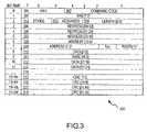
- FIG. 3depicts a write command packet 300 including a hint 301 .
- the write command packet 300is generated by the controller 128 and communicated to the hub 140 .
- the packet 300includes the hint 301 and a command code 302 .
- the write command packet 300further includes write data 310 , write address information 305 , and may include other information such as a tag 311 , a stride 312 , a reservation 313 , a length 314 , and error check information 315 .
- FIG. 4depicts a read command packet 350 including a hint 351 .
- the read command packet 350is generated by the controller 128 and communicated to the hub 140 .
- the packet 350includes the hint 351 and a command code 352 .
- the read command packet 350further includes read address information 355 , and may include other information such as a tag 361 , a stride 362 , a reservation 363 , a length 364 , and error check information 365 .
- Read and write command packetsare sent to the hub 140 .
- One implementation of the hub 140 for receiving the packets 300 and/or 350is shown in FIG. 5 .
- a read or write packetis received from a link in 400 .
- a request decoder 405receives the packet and decodes the request and any hint or hints, which are provided to request queue 410 .
- the request decoder 405further decodes a read address, and provides the read address to a comparator 415 .
- a write buffer queue 420further receives packets from the link in 400 and provides a write address to the comparator 415 .
- the comparator 415compares the read and write addresses, and notifies the request queue 410 of any write conflicts.
- the request queue 410accesses a prefetch buffer 425 to fulfill the request.
- Requests and hintsare provided to a memory sequencer 430 connected to a memory interface 435 .
- the memory sequencer 430acts on any hint information, and sends request over the memory interface 435 .
- Memory read dataare coupled into the prefetch buffer 425 for storage, if appropriate.
Landscapes
- Engineering & Computer Science (AREA)
- Theoretical Computer Science (AREA)
- Physics & Mathematics (AREA)
- General Engineering & Computer Science (AREA)
- General Physics & Mathematics (AREA)
- Memory System Of A Hierarchy Structure (AREA)
- Bus Control (AREA)
Abstract
Description
Claims (34)
Priority Applications (1)
| Application Number | Priority Date | Filing Date | Title |
|---|---|---|---|
| US11/408,285US7418526B2 (en) | 2004-03-29 | 2006-04-19 | Memory hub and method for providing memory sequencing hints |
Applications Claiming Priority (2)
| Application Number | Priority Date | Filing Date | Title |
|---|---|---|---|
| US10/812,950US7213082B2 (en) | 2004-03-29 | 2004-03-29 | Memory hub and method for providing memory sequencing hints |
| US11/408,285US7418526B2 (en) | 2004-03-29 | 2006-04-19 | Memory hub and method for providing memory sequencing hints |
Related Parent Applications (1)
| Application Number | Title | Priority Date | Filing Date |
|---|---|---|---|
| US10/812,950ContinuationUS7213082B2 (en) | 2004-03-29 | 2004-03-29 | Memory hub and method for providing memory sequencing hints |
Publications (2)
| Publication Number | Publication Date |
|---|---|
| US20060212666A1 US20060212666A1 (en) | 2006-09-21 |
| US7418526B2true US7418526B2 (en) | 2008-08-26 |
Family
ID=34991517
Family Applications (2)
| Application Number | Title | Priority Date | Filing Date |
|---|---|---|---|
| US10/812,950Expired - Fee RelatedUS7213082B2 (en) | 2004-03-29 | 2004-03-29 | Memory hub and method for providing memory sequencing hints |
| US11/408,285Expired - Fee RelatedUS7418526B2 (en) | 2004-03-29 | 2006-04-19 | Memory hub and method for providing memory sequencing hints |
Family Applications Before (1)
| Application Number | Title | Priority Date | Filing Date |
|---|---|---|---|
| US10/812,950Expired - Fee RelatedUS7213082B2 (en) | 2004-03-29 | 2004-03-29 | Memory hub and method for providing memory sequencing hints |
Country Status (6)
| Country | Link |
|---|---|
| US (2) | US7213082B2 (en) |
| EP (1) | EP1738265A4 (en) |
| JP (1) | JP2007535737A (en) |
| KR (1) | KR100860956B1 (en) |
| CN (1) | CN101427224A (en) |
| WO (1) | WO2005098629A2 (en) |
Cited By (21)
| Publication number | Priority date | Publication date | Assignee | Title |
|---|---|---|---|---|
| US20070204116A1 (en)* | 2006-02-27 | 2007-08-30 | Qimonda Ag | Memory arrangement |
| US20070276976A1 (en)* | 2006-05-24 | 2007-11-29 | International Business Machines Corporation | Systems and methods for providing distributed technology independent memory controllers |
| US20080183977A1 (en)* | 2007-01-29 | 2008-07-31 | International Business Machines Corporation | Systems and methods for providing a dynamic memory bank page policy |
| US7581073B2 (en) | 2006-08-09 | 2009-08-25 | International Business Machines Corporation | Systems and methods for providing distributed autonomous power management in a memory system |
| US7584336B2 (en) | 2006-06-08 | 2009-09-01 | International Business Machines Corporation | Systems and methods for providing data modification operations in memory subsystems |
| US7587559B2 (en) | 2006-08-10 | 2009-09-08 | International Business Machines Corporation | Systems and methods for memory module power management |
| US7603526B2 (en) | 2007-01-29 | 2009-10-13 | International Business Machines Corporation | Systems and methods for providing dynamic memory pre-fetch |
| US7610423B2 (en) | 2004-10-29 | 2009-10-27 | International Business Machines Corporation | Service interface to a memory system |
| US7636813B2 (en) | 2006-05-22 | 2009-12-22 | International Business Machines Corporation | Systems and methods for providing remote pre-fetch buffers |
| US7636833B2 (en) | 2006-08-15 | 2009-12-22 | International Business Machines Corporation | Method for selecting memory busses according to physical memory organization information associated with virtual address translation tables |
| US7640386B2 (en) | 2006-05-24 | 2009-12-29 | International Business Machines Corporation | Systems and methods for providing memory modules with multiple hub devices |
| US7669086B2 (en) | 2006-08-02 | 2010-02-23 | International Business Machines Corporation | Systems and methods for providing collision detection in a memory system |
| US7685392B2 (en) | 2005-11-28 | 2010-03-23 | International Business Machines Corporation | Providing indeterminate read data latency in a memory system |
| US7721140B2 (en) | 2007-01-02 | 2010-05-18 | International Business Machines Corporation | Systems and methods for improving serviceability of a memory system |
| US7765368B2 (en) | 2004-07-30 | 2010-07-27 | International Business Machines Corporation | System, method and storage medium for providing a serialized memory interface with a bus repeater |
| US7844771B2 (en) | 2004-10-29 | 2010-11-30 | International Business Machines Corporation | System, method and storage medium for a memory subsystem command interface |
| US7870459B2 (en) | 2006-10-23 | 2011-01-11 | International Business Machines Corporation | High density high reliability memory module with power gating and a fault tolerant address and command bus |
| US7934115B2 (en) | 2005-10-31 | 2011-04-26 | International Business Machines Corporation | Deriving clocks in a memory system |
| US8140942B2 (en) | 2004-10-29 | 2012-03-20 | International Business Machines Corporation | System, method and storage medium for providing fault detection and correction in a memory subsystem |
| US8239607B2 (en) | 2004-06-04 | 2012-08-07 | Micron Technology, Inc. | System and method for an asynchronous data buffer having buffer write and read pointers |
| US8296541B2 (en) | 2004-10-29 | 2012-10-23 | International Business Machines Corporation | Memory subsystem with positional read data latency |
Families Citing this family (32)
| Publication number | Priority date | Publication date | Assignee | Title |
|---|---|---|---|---|
| US6791555B1 (en) | 2000-06-23 | 2004-09-14 | Micron Technology, Inc. | Apparatus and method for distributed memory control in a graphics processing system |
| US7133972B2 (en) | 2002-06-07 | 2006-11-07 | Micron Technology, Inc. | Memory hub with internal cache and/or memory access prediction |
| US7117316B2 (en)* | 2002-08-05 | 2006-10-03 | Micron Technology, Inc. | Memory hub and access method having internal row caching |
| US6820181B2 (en)* | 2002-08-29 | 2004-11-16 | Micron Technology, Inc. | Method and system for controlling memory accesses to memory modules having a memory hub architecture |
| US7120727B2 (en) | 2003-06-19 | 2006-10-10 | Micron Technology, Inc. | Reconfigurable memory module and method |
| US7260685B2 (en) | 2003-06-20 | 2007-08-21 | Micron Technology, Inc. | Memory hub and access method having internal prefetch buffers |
| US7107415B2 (en) | 2003-06-20 | 2006-09-12 | Micron Technology, Inc. | Posted write buffers and methods of posting write requests in memory modules |
| US7133991B2 (en)* | 2003-08-20 | 2006-11-07 | Micron Technology, Inc. | Method and system for capturing and bypassing memory transactions in a hub-based memory system |
| US7120743B2 (en) | 2003-10-20 | 2006-10-10 | Micron Technology, Inc. | Arbitration system and method for memory responses in a hub-based memory system |
| US7330992B2 (en) | 2003-12-29 | 2008-02-12 | Micron Technology, Inc. | System and method for read synchronization of memory modules |
| US7188219B2 (en) | 2004-01-30 | 2007-03-06 | Micron Technology, Inc. | Buffer control system and method for a memory system having outstanding read and write request buffers |
| US7366864B2 (en) | 2004-03-08 | 2008-04-29 | Micron Technology, Inc. | Memory hub architecture having programmable lane widths |
| US7162567B2 (en) | 2004-05-14 | 2007-01-09 | Micron Technology, Inc. | Memory hub and method for memory sequencing |
| US7389375B2 (en) | 2004-07-30 | 2008-06-17 | International Business Machines Corporation | System, method and storage medium for a multi-mode memory buffer device |
| US7539800B2 (en) | 2004-07-30 | 2009-05-26 | International Business Machines Corporation | System, method and storage medium for providing segment level sparing |
| KR100551480B1 (en)* | 2004-10-25 | 2006-02-13 | 삼성전자주식회사 | A memory device located between the processor and the nonvolatile memory, a system including the same, and a data transmission / reception method within the system |
| US7305574B2 (en) | 2004-10-29 | 2007-12-04 | International Business Machines Corporation | System, method and storage medium for bus calibration in a memory subsystem |
| US7328381B2 (en)* | 2005-08-01 | 2008-02-05 | Micron Technology, Inc. | Testing system and method for memory modules having a memory hub architecture |
| US7319340B2 (en)* | 2005-08-01 | 2008-01-15 | Micron Technology, Inc. | Integrated circuit load board and method having on-board test circuit |
| US7765424B2 (en)* | 2005-08-19 | 2010-07-27 | Micron Technology, Inc. | System and method for injecting phase jitter into integrated circuit test signals |
| US7355387B2 (en) | 2005-12-08 | 2008-04-08 | Micron Technology, Inc. | System and method for testing integrated circuit timing margins |
| US7725654B2 (en)* | 2006-07-25 | 2010-05-25 | Hewlett-Packard Development Company, L.P. | Affecting a caching algorithm used by a cache of storage system |
| US8032711B2 (en)* | 2006-12-22 | 2011-10-04 | Intel Corporation | Prefetching from dynamic random access memory to a static random access memory |
| US7870351B2 (en)* | 2007-11-15 | 2011-01-11 | Micron Technology, Inc. | System, apparatus, and method for modifying the order of memory accesses |
| WO2011094436A2 (en)* | 2010-01-28 | 2011-08-04 | Hewlett-Packard Development Company, L.P. | Interface methods and apparatus for memory devices |
| US20160246711A9 (en)* | 2010-01-28 | 2016-08-25 | Hewlett-Packard Development Company, L. P. | Interface methods and apparatus for memory devices |
| US8938589B2 (en) | 2010-01-28 | 2015-01-20 | Hewlett-Packard Development Company, L. P. | Interface methods and apparatus for memory devices using arbitration |
| US9251048B2 (en)* | 2012-10-19 | 2016-02-02 | International Business Machines Corporation | Memory page management |
| US9367474B2 (en) | 2013-06-12 | 2016-06-14 | Apple Inc. | Translating cache hints |
| WO2019005105A1 (en)* | 2017-06-30 | 2019-01-03 | Intel Corporation | Speculative memory activation |
| US10613764B2 (en) | 2017-11-20 | 2020-04-07 | Advanced Micro Devices, Inc. | Speculative hint-triggered activation of pages in memory |
| US11093393B2 (en)* | 2018-12-27 | 2021-08-17 | Samsung Electronics Co., Ltd. | System and method for early DRAM page-activation |
Citations (259)
| Publication number | Priority date | Publication date | Assignee | Title |
|---|---|---|---|---|
| US3742253A (en) | 1971-03-15 | 1973-06-26 | Burroughs Corp | Three state logic device with applications |
| US4045781A (en) | 1976-02-13 | 1977-08-30 | Digital Equipment Corporation | Memory module with selectable byte addressing for digital data processing system |
| US4240143A (en) | 1978-12-22 | 1980-12-16 | Burroughs Corporation | Hierarchical multi-processor network for memory sharing |
| US4245306A (en) | 1978-12-21 | 1981-01-13 | Burroughs Corporation | Selection of addressed processor in a multi-processor network |
| US4253144A (en) | 1978-12-21 | 1981-02-24 | Burroughs Corporation | Multi-processor communication network |
| US4253146A (en) | 1978-12-21 | 1981-02-24 | Burroughs Corporation | Module for coupling computer-processors |
| US4608702A (en) | 1984-12-21 | 1986-08-26 | Advanced Micro Devices, Inc. | Method for digital clock recovery from Manchester-encoded signals |
| US4707823A (en) | 1986-07-21 | 1987-11-17 | Chrysler Motors Corporation | Fiber optic multiplexed data acquisition system |
| US4724520A (en) | 1985-07-01 | 1988-02-09 | United Technologies Corporation | Modular multiport data hub |
| US4831520A (en) | 1987-02-24 | 1989-05-16 | Digital Equipment Corporation | Bus interface circuit for digital data processor |
| US4891808A (en) | 1987-12-24 | 1990-01-02 | Coherent Communication Systems Corp. | Self-synchronizing multiplexer |
| US4930128A (en) | 1987-06-26 | 1990-05-29 | Hitachi, Ltd. | Method for restart of online computer system and apparatus for carrying out the same |
| US4953930A (en) | 1989-03-15 | 1990-09-04 | Ramtech, Inc. | CPU socket supporting socket-to-socket optical communications |
| US5133059A (en)* | 1987-07-30 | 1992-07-21 | Alliant Computer Systems Corporation | Computer with multiple processors having varying priorities for access to a multi-element memory |
| US5241506A (en) | 1989-11-15 | 1993-08-31 | Kabushiki Kaisha Toshiba | Semiconductor memory circuit apparatus |
| US5243703A (en) | 1990-04-18 | 1993-09-07 | Rambus, Inc. | Apparatus for synchronously generating clock signals in a data processing system |
| WO1993019422A1 (en) | 1992-03-25 | 1993-09-30 | Encore Computer U.S., Inc. | Fiber optic memory coupling system |
| US5251303A (en) | 1989-01-13 | 1993-10-05 | International Business Machines Corporation | System for DMA block data transfer based on linked control blocks |
| US5269022A (en) | 1990-03-28 | 1993-12-07 | Kabushiki Kaisha Toshiba | Method and apparatus for booting a computer system by restoring the main memory from a backup memory |
| US5313590A (en) | 1990-01-05 | 1994-05-17 | Maspar Computer Corporation | System having fixedly priorized and grouped by positions I/O lines for interconnecting router elements in plurality of stages within parrallel computer |
| US5317752A (en) | 1989-12-22 | 1994-05-31 | Tandem Computers Incorporated | Fault-tolerant computer system with auto-restart after power-fall |
| US5319755A (en) | 1990-04-18 | 1994-06-07 | Rambus, Inc. | Integrated circuit I/O using high performance bus interface |
| US5327553A (en) | 1989-12-22 | 1994-07-05 | Tandem Computers Incorporated | Fault-tolerant computer system with /CONFIG filesystem |
| US5355391A (en) | 1992-03-06 | 1994-10-11 | Rambus, Inc. | High speed bus system |
| US5432823A (en) | 1992-03-06 | 1995-07-11 | Rambus, Inc. | Method and circuitry for minimizing clock-data skew in a bus system |
| US5432907A (en) | 1992-05-12 | 1995-07-11 | Network Resources Corporation | Network hub with integrated bridge |
| US5442770A (en) | 1989-01-24 | 1995-08-15 | Nec Electronics, Inc. | Triple port cache memory |
| US5461627A (en) | 1991-12-24 | 1995-10-24 | Rypinski; Chandos A. | Access protocol for a common channel wireless network |
| US5465229A (en) | 1992-05-19 | 1995-11-07 | Sun Microsystems, Inc. | Single in-line memory module |
| US5479370A (en) | 1992-02-20 | 1995-12-26 | Kabushiki Kaisha Toshiba | Semiconductor memory with bypass circuit |
| US5497476A (en) | 1992-09-21 | 1996-03-05 | International Business Machines Corporation | Scatter-gather in data processing system |
| US5502621A (en) | 1994-03-31 | 1996-03-26 | Hewlett-Packard Company | Mirrored pin assignment for two sided multi-chip layout |
| US5566325A (en) | 1994-06-30 | 1996-10-15 | Digital Equipment Corporation | Method and apparatus for adaptive memory access |
| US5577220A (en) | 1993-07-23 | 1996-11-19 | International Business Machines Corporation | Method for saving and restoring the state of a CPU executing code in protected mode including estimating the value of the page table base register |
| US5581767A (en) | 1993-06-16 | 1996-12-03 | Nippon Sheet Glass Co., Ltd. | Bus structure for multiprocessor system having separated processor section and control/memory section |
| US5638534A (en) | 1995-03-31 | 1997-06-10 | Samsung Electronics Co., Ltd. | Memory controller which executes read and write commands out of order |
| US5659798A (en) | 1996-02-02 | 1997-08-19 | Blumrich; Matthias Augustin | Method and system for initiating and loading DMA controller registers by using user-level programs |
| US5687325A (en) | 1996-04-19 | 1997-11-11 | Chang; Web | Application specific field programmable gate array |
| US5706224A (en) | 1996-10-10 | 1998-01-06 | Quality Semiconductor, Inc. | Content addressable memory and random access memory partition circuit |
| US5710733A (en) | 1996-01-22 | 1998-01-20 | Silicon Graphics, Inc. | Processor-inclusive memory module |
| US5715456A (en) | 1995-02-13 | 1998-02-03 | International Business Machines Corporation | Method and apparatus for booting a computer system without pre-installing an operating system |
| US5729709A (en) | 1993-11-12 | 1998-03-17 | Intel Corporation | Memory controller with burst addressing circuit |
| US5748616A (en) | 1994-09-13 | 1998-05-05 | Square D Company | Data link module for time division multiplexing control systems |
| EP0849685A2 (en) | 1996-12-19 | 1998-06-24 | Texas Instruments Incorporated | Communication bus system between processors and memory modules |
| US5796413A (en) | 1995-12-06 | 1998-08-18 | Compaq Computer Corporation | Graphics controller utilizing video memory to provide macro command capability and enhanched command buffering |
| US5818844A (en) | 1996-06-06 | 1998-10-06 | Advanced Micro Devices, Inc. | Address generation and data path arbitration to and from SRAM to accommodate multiple transmitted packets |
| US5819304A (en) | 1996-01-29 | 1998-10-06 | Iowa State University Research Foundation, Inc. | Random access memory assembly |
| US5822255A (en) | 1996-08-13 | 1998-10-13 | Fujitsu Limited | Semiconductor integrated circuit for supplying a control signal to a plurality of object circuits |
| US5832250A (en) | 1996-01-26 | 1998-11-03 | Unisys Corporation | Multi set cache structure having parity RAMs holding parity bits for tag data and for status data utilizing prediction circuitry that predicts and generates the needed parity bits |
| US5875454A (en) | 1996-07-24 | 1999-02-23 | International Business Machiness Corporation | Compressed data cache storage system |
| US5875352A (en) | 1995-11-03 | 1999-02-23 | Sun Microsystems, Inc. | Method and apparatus for multiple channel direct memory access control |
| US5887159A (en) | 1996-12-11 | 1999-03-23 | Digital Equipment Corporation | Dynamically determining instruction hint fields |
| US5966724A (en) | 1996-01-11 | 1999-10-12 | Micron Technology, Inc. | Synchronous memory device with dual page and burst mode operations |
| US5973935A (en) | 1997-04-07 | 1999-10-26 | Micron Technology, Inc. | Interdigitated leads-over-chip lead frame for supporting an integrated circuit die |
| US5978567A (en) | 1994-07-27 | 1999-11-02 | Instant Video Technologies Inc. | System for distribution of interactive multimedia and linear programs by enabling program webs which include control scripts to define presentation by client transceiver |
| US5987196A (en) | 1997-11-06 | 1999-11-16 | Micron Technology, Inc. | Semiconductor structure having an optical signal path in a substrate and method for forming the same |
| US6011741A (en) | 1991-04-11 | 2000-01-04 | Sandisk Corporation | Computer memory cards using flash EEPROM integrated circuit chips and memory-controller systems |
| US6023726A (en) | 1998-01-20 | 2000-02-08 | Netscape Communications Corporation | User configurable prefetch control system for enabling client to prefetch documents from a network server |
| US6029250A (en) | 1998-09-09 | 2000-02-22 | Micron Technology, Inc. | Method and apparatus for adaptively adjusting the timing offset between a clock signal and digital signals transmitted coincident with that clock signal, and memory device and system using same |
| US6031241A (en) | 1997-03-11 | 2000-02-29 | University Of Central Florida | Capillary discharge extreme ultraviolet lamp source for EUV microlithography and other related applications |
| US6033951A (en) | 1996-08-16 | 2000-03-07 | United Microelectronics Corp. | Process for fabricating a storage capacitor for semiconductor memory devices |
| US6038630A (en) | 1998-03-24 | 2000-03-14 | International Business Machines Corporation | Shared access control device for integrated system with multiple functional units accessing external structures over multiple data buses |
| US6061263A (en) | 1998-12-29 | 2000-05-09 | Intel Corporation | Small outline rambus in-line memory module |
| US6061296A (en) | 1998-08-17 | 2000-05-09 | Vanguard International Semiconductor Corporation | Multiple data clock activation with programmable delay for use in multiple CAS latency memory devices |
| US6067649A (en) | 1998-06-10 | 2000-05-23 | Compaq Computer Corporation | Method and apparatus for a low power self test of a memory subsystem |
| US6067262A (en) | 1998-12-11 | 2000-05-23 | Lsi Logic Corporation | Redundancy analysis for embedded memories with built-in self test and built-in self repair |
| US6073190A (en) | 1997-07-18 | 2000-06-06 | Micron Electronics, Inc. | System for dynamic buffer allocation comprising control logic for controlling a first address buffer and a first data buffer as a matched pair |
| US6076139A (en) | 1996-12-31 | 2000-06-13 | Compaq Computer Corporation | Multimedia computer architecture with multi-channel concurrent memory access |
| US6079008A (en) | 1998-04-03 | 2000-06-20 | Patton Electronics Co. | Multiple thread multiple data predictive coded parallel processing system and method |
| US6092158A (en) | 1997-06-13 | 2000-07-18 | Intel Corporation | Method and apparatus for arbitrating between command streams |
| US6098158A (en) | 1997-12-18 | 2000-08-01 | International Business Machines Corporation | Software-enabled fast boot |
| US6105075A (en) | 1997-08-05 | 2000-08-15 | Adaptec, Inc. | Scatter gather memory system for a hardware accelerated command interpreter engine |
| US6125431A (en) | 1996-08-02 | 2000-09-26 | Oki Electric Industry Co., Ltd. | Single-chip microcomputer using adjustable timing to fetch data from an external memory |
| US6128703A (en) | 1997-09-05 | 2000-10-03 | Integrated Device Technology, Inc. | Method and apparatus for memory prefetch operation of volatile non-coherent data |
| US6128706A (en)* | 1998-02-03 | 2000-10-03 | Institute For The Development Of Emerging Architectures, L.L.C. | Apparatus and method for a load bias--load with intent to semaphore |
| US6131149A (en) | 1997-06-04 | 2000-10-10 | Oak Technology, Inc. | Apparatus and method for reading data from synchronous memory with skewed clock pulses |
| US6134624A (en) | 1998-06-08 | 2000-10-17 | Storage Technology Corporation | High bandwidth cache system |
| US6145033A (en) | 1998-07-17 | 2000-11-07 | Seiko Epson Corporation | Management of display FIFO requests for DRAM access wherein low priority requests are initiated when FIFO level is below/equal to high threshold value |
| US6144587A (en) | 1998-06-23 | 2000-11-07 | Nec Corporation | Semiconductor memory device |
| US6157962A (en) | 1996-02-05 | 2000-12-05 | International Business Machines Corporation | Multipath I/O storage systems with multiipath I/O request mechanisms |
| US6157743A (en) | 1998-07-31 | 2000-12-05 | Hewlett Packard Company | Method for retrieving compressed texture data from a memory system |
| US6167486A (en) | 1996-11-18 | 2000-12-26 | Nec Electronics, Inc. | Parallel access virtual channel memory system with cacheable channels |
| US6167465A (en) | 1998-05-20 | 2000-12-26 | Aureal Semiconductor, Inc. | System for managing multiple DMA connections between a peripheral device and a memory and performing real-time operations on data carried by a selected DMA connection |
| US6175571B1 (en) | 1994-07-22 | 2001-01-16 | Network Peripherals, Inc. | Distributed memory switching hub |
| US6185352B1 (en) | 2000-02-24 | 2001-02-06 | Siecor Operations, Llc | Optical fiber ribbon fan-out cables |
| US6185676B1 (en) | 1997-09-30 | 2001-02-06 | Intel Corporation | Method and apparatus for performing early branch prediction in a microprocessor |
| US6186400B1 (en) | 1998-03-20 | 2001-02-13 | Symbol Technologies, Inc. | Bar code reader with an integrated scanning component module mountable on printed circuit board |
| US6191663B1 (en) | 1998-12-22 | 2001-02-20 | Intel Corporation | Echo reduction on bit-serial, multi-drop bus |
| US6201724B1 (en) | 1998-11-12 | 2001-03-13 | Nec Corporation | Semiconductor memory having improved register array access speed |
| US6208180B1 (en) | 1995-12-29 | 2001-03-27 | Intel Corporation | Core clock correction in a 2/N mode clocking scheme |
| US6212590B1 (en) | 1997-12-22 | 2001-04-03 | Compaq Computer Corporation | Computer system having integrated bus bridge design with delayed transaction arbitration mechanism employed within laptop computer docked to expansion base |
| US6219725B1 (en) | 1998-08-28 | 2001-04-17 | Hewlett-Packard Company | Method and apparatus for performing direct memory access transfers involving non-sequentially-addressable memory locations |
| US6223301B1 (en) | 1997-09-30 | 2001-04-24 | Compaq Computer Corporation | Fault tolerant memory |
| US6233376B1 (en) | 1999-05-18 | 2001-05-15 | The United States Of America As Represented By The Secretary Of The Navy | Embedded fiber optic circuit boards and integrated circuits |
| US6243769B1 (en) | 1997-07-18 | 2001-06-05 | Micron Technology, Inc. | Dynamic buffer allocation for a computer system |
| US6243831B1 (en) | 1998-10-31 | 2001-06-05 | Compaq Computer Corporation | Computer system with power loss protection mechanism |
| US6246618B1 (en) | 2000-06-30 | 2001-06-12 | Mitsubishi Denki Kabushiki Kaisha | Semiconductor integrated circuit capable of testing and substituting defective memories and method thereof |
| US6247107B1 (en) | 1998-04-06 | 2001-06-12 | Advanced Micro Devices, Inc. | Chipset configured to perform data-directed prefetching |
| US6249802B1 (en) | 1997-09-19 | 2001-06-19 | Silicon Graphics, Inc. | Method, system, and computer program product for allocating physical memory in a distributed shared memory network |
| US6252821B1 (en) | 1999-12-29 | 2001-06-26 | Intel Corporation | Method and apparatus for memory address decode in memory subsystems supporting a large number of memory devices |
| US6256692B1 (en) | 1997-10-13 | 2001-07-03 | Fujitsu Limited | CardBus interface circuit, and a CardBus PC having the same |
| US6272609B1 (en) | 1998-07-31 | 2001-08-07 | Micron Electronics, Inc. | Pipelined memory controller |
| US6286083B1 (en) | 1998-07-08 | 2001-09-04 | Compaq Computer Corporation | Computer system with adaptive memory arbitration scheme |
| US6285349B1 (en) | 1999-02-26 | 2001-09-04 | Intel Corporation | Correcting non-uniformity in displays |
| US6294937B1 (en) | 1999-05-25 | 2001-09-25 | Lsi Logic Corporation | Method and apparatus for self correcting parallel I/O circuitry |
| JP2001265539A (en) | 2000-03-16 | 2001-09-28 | Fuji Xerox Co Ltd | Array type storage device and information processing system |
| US6301637B1 (en) | 1998-06-08 | 2001-10-09 | Storage Technology Corporation | High performance data paths |
| US20010039612A1 (en) | 1999-12-02 | 2001-11-08 | Lee Sang-Jin | Apparatus and method for fast booting |
| US6330205B2 (en) | 1999-12-22 | 2001-12-11 | Nec Corporation | Virtual channel synchronous dynamic random access memory |
| US6347055B1 (en) | 1999-06-24 | 2002-02-12 | Nec Corporation | Line buffer type semiconductor memory device capable of direct prefetch and restore operations |
| US6349363B2 (en) | 1998-12-08 | 2002-02-19 | Intel Corporation | Multi-section cache with different attributes for each section |
| US6356573B1 (en) | 1998-01-31 | 2002-03-12 | Mitel Semiconductor Ab | Vertical cavity surface emitting laser |
| US6367074B1 (en) | 1998-12-28 | 2002-04-02 | Intel Corporation | Operation of a system |
| WO2002027499A2 (en) | 2000-09-29 | 2002-04-04 | Intel Corporation | Shared translation address caching |
| US6370068B2 (en) | 2000-01-05 | 2002-04-09 | Samsung Electronics Co., Ltd. | Semiconductor memory devices and methods for sampling data therefrom based on a relative position of a memory cell array section containing the data |
| US6370611B1 (en) | 2000-04-04 | 2002-04-09 | Compaq Computer Corporation | Raid XOR operations to synchronous DRAM using a read buffer and pipelining of synchronous DRAM burst read data |
| US6373777B1 (en) | 1998-07-14 | 2002-04-16 | Nec Corporation | Semiconductor memory |
| US6381190B1 (en) | 1999-05-13 | 2002-04-30 | Nec Corporation | Semiconductor memory device in which use of cache can be selected |
| US6389514B1 (en) | 1999-03-25 | 2002-05-14 | Hewlett-Packard Company | Method and computer system for speculatively closing pages in memory |
| US6392653B1 (en) | 1998-06-25 | 2002-05-21 | Inria Institut National De Recherche En Informatique Et En Automatique | Device for processing acquisition data, in particular image data |
| US6401213B1 (en) | 1999-07-09 | 2002-06-04 | Micron Technology, Inc. | Timing circuit for high speed memory |
| US6405280B1 (en) | 1998-06-05 | 2002-06-11 | Micron Technology, Inc. | Packet-oriented synchronous DRAM interface supporting a plurality of orderings for data block transfers within a burst sequence |
| US6421744B1 (en) | 1999-10-25 | 2002-07-16 | Motorola, Inc. | Direct memory access controller and method therefor |
| US6430696B1 (en) | 1998-11-30 | 2002-08-06 | Micron Technology, Inc. | Method and apparatus for high speed data capture utilizing bit-to-bit timing correction, and memory device using same |
| US6434696B1 (en) | 1998-05-11 | 2002-08-13 | Lg Electronics Inc. | Method for quickly booting a computer system |
| US6433785B1 (en) | 1999-04-09 | 2002-08-13 | Intel Corporation | Method and apparatus for improving processor to graphics device throughput |
| US6434736B1 (en) | 1999-07-08 | 2002-08-13 | Intel Corporation | Location based timing scheme in memory design |
| US6434639B1 (en) | 1998-11-13 | 2002-08-13 | Intel Corporation | System for combining requests associated with one or more memory locations that are collectively associated with a single cache line to furnish a single memory operation |
| US20020112119A1 (en) | 1998-02-13 | 2002-08-15 | Intel Corporation | Dual-port buffer-to-memory interface |
| US6438622B1 (en) | 1998-11-17 | 2002-08-20 | Intel Corporation | Multiprocessor system including a docking system |
| US6438668B1 (en) | 1999-09-30 | 2002-08-20 | Apple Computer, Inc. | Method and apparatus for reducing power consumption in a digital processing system |
| US20020116588A1 (en) | 2000-12-20 | 2002-08-22 | Beckert Richard Dennis | Software management systems and methods for automotive computing devices |
| US20020120709A1 (en) | 2001-02-13 | 2002-08-29 | Matsushita Electric Industrial Co., Ltd. | Shared-memory controller for use in a multimedia processor system |
| US6449308B1 (en) | 1999-05-25 | 2002-09-10 | Intel Corporation | High-speed digital distribution system |
| US6453393B1 (en) | 2000-09-18 | 2002-09-17 | Intel Corporation | Method and apparatus for interfacing to a computer memory |
| US6460114B1 (en) | 1999-07-29 | 2002-10-01 | Micron Technology, Inc. | Storing a flushed cache line in a memory buffer of a controller |
| US6460108B1 (en) | 1999-03-31 | 2002-10-01 | Intel Corporation | Low cost data streaming mechanism |
| US20020144064A1 (en) | 2001-03-30 | 2002-10-03 | Fanning Blaise B. | Controlling cache memory in external chipset using processor |
| US6462978B2 (en) | 1997-08-21 | 2002-10-08 | Hitachi, Ltd. | Method of designing semiconductor integrated circuit device and semiconductor integrated circuit device |
| US6463059B1 (en) | 1998-12-04 | 2002-10-08 | Koninklijke Philips Electronics N.V. | Direct memory access execution engine with indirect addressing of circular queues in addition to direct memory addressing |
| US6467013B1 (en) | 1999-09-30 | 2002-10-15 | Intel Corporation | Memory transceiver to couple an additional memory channel to an existing memory channel |
| US6473828B1 (en) | 1998-07-03 | 2002-10-29 | Nec Corporation | Virtual channel synchronous dynamic random access memory |
| US6477614B1 (en) | 1998-09-30 | 2002-11-05 | Intel Corporation | Method for implementing multiple memory buses on a memory module |
| US6477592B1 (en) | 1999-08-06 | 2002-11-05 | Integrated Memory Logic, Inc. | System for I/O interfacing for semiconductor chip utilizing addition of reference element to each data element in first data stream and interpret to recover data elements of second data stream |
| US6479322B2 (en) | 1998-06-01 | 2002-11-12 | Hitachi, Ltd. | Semiconductor device with two stacked chips in one resin body and method of producing |
| US6487628B1 (en) | 1999-03-31 | 2002-11-26 | Compaq Computer Corporation | Peripheral component interface with multiple data channels and reduced latency over a system area network |
| US6487556B1 (en) | 1998-12-18 | 2002-11-26 | International Business Machines Corporation | Method and system for providing an associative datastore within a data processing system |
| US20020178319A1 (en) | 2001-05-24 | 2002-11-28 | Jorge Sanchez-Olea | Optical bus arrangement for computer system |
| US6490188B2 (en) | 1999-09-02 | 2002-12-03 | Micron Technology, Inc. | Semiconductor devices having mirrored terminal arrangements, devices including same, and methods of testing such semiconductor devices |
| US6493803B1 (en) | 1999-08-23 | 2002-12-10 | Advanced Micro Devices, Inc. | Direct memory access controller with channel width configurability support |
| US6496909B1 (en) | 1999-04-06 | 2002-12-17 | Silicon Graphics, Inc. | Method for managing concurrent access to virtual memory data structures |
| US6496193B1 (en) | 1999-12-30 | 2002-12-17 | Intel Corporation | Method and apparatus for fast loading of texture data into a tiled memory |
| US6501471B1 (en) | 1999-12-13 | 2002-12-31 | Intel Corporation | Volume rendering |
| US6502161B1 (en) | 2000-01-05 | 2002-12-31 | Rambus Inc. | Memory system including a point-to-point linked memory subsystem |
| US20030005223A1 (en) | 2001-06-27 | 2003-01-02 | Coulson Richard L. | System boot time reduction method |
| US6505287B2 (en) | 1999-12-20 | 2003-01-07 | Nec Corporation | Virtual channel memory access controlling circuit |
| US20030014578A1 (en) | 2001-07-11 | 2003-01-16 | Pax George E. | Routability for memeory devices |
| US6523093B1 (en) | 2000-09-29 | 2003-02-18 | Intel Corporation | Prefetch buffer allocation and filtering system |
| US6523092B1 (en) | 2000-09-29 | 2003-02-18 | Intel Corporation | Cache line replacement policy enhancement to avoid memory page thrashing |
| US6526483B1 (en) | 2000-09-20 | 2003-02-25 | Broadcom Corporation | Page open hint in transactions |
| US20030043158A1 (en) | 2001-05-18 | 2003-03-06 | Wasserman Michael A. | Method and apparatus for reducing inefficiencies in shared memory devices |
| US20030043426A1 (en) | 2001-08-30 | 2003-03-06 | Baker R. J. | Optical interconnect in high-speed memory systems |
| US6539490B1 (en) | 1999-08-30 | 2003-03-25 | Micron Technology, Inc. | Clock distribution without clock delay or skew |
| US6552564B1 (en) | 1999-08-30 | 2003-04-22 | Micron Technology, Inc. | Technique to reduce reflections and ringing on CMOS interconnections |
| US6564329B1 (en) | 1999-03-16 | 2003-05-13 | Linkup Systems Corporation | System and method for dynamic clock generation |
| US20030093630A1 (en) | 2001-11-15 | 2003-05-15 | Richard Elizabeth A. | Techniques for processing out-of -order requests in a processor-based system |
| US6590816B2 (en) | 2001-03-05 | 2003-07-08 | Infineon Technologies Ag | Integrated memory and method for testing and repairing the integrated memory |
| US6594722B1 (en) | 2000-06-29 | 2003-07-15 | Intel Corporation | Mechanism for managing multiple out-of-order packet streams in a PCI host bridge |
| US6594713B1 (en) | 1999-09-10 | 2003-07-15 | Texas Instruments Incorporated | Hub interface unit and application unit interfaces for expanded direct memory access processor |
| US6598154B1 (en) | 1998-12-29 | 2003-07-22 | Intel Corporation | Precoding branch instructions to reduce branch-penalty in pipelined processors |
| US20030149809A1 (en) | 2001-08-29 | 2003-08-07 | Jensen Poul R. | Method and apparatus for timing and event processing in wireless systems |
| US20030156639A1 (en) | 2002-02-19 | 2003-08-21 | Jui Liang | Frame rate control system and method |
| US20030163649A1 (en) | 2002-02-25 | 2003-08-28 | Kapur Suvansh K. | Shared bypass bus structure |
| US6615325B2 (en) | 1996-01-11 | 2003-09-02 | Micron Technology, Inc. | Method for switching between modes of operation |
| US6622227B2 (en) | 2000-12-27 | 2003-09-16 | Intel Corporation | Method and apparatus for utilizing write buffers in memory control/interface |
| US6628294B1 (en) | 1999-12-31 | 2003-09-30 | Intel Corporation | Prefetching of virtual-to-physical address translation for display data |
| US6629220B1 (en) | 1999-08-20 | 2003-09-30 | Intel Corporation | Method and apparatus for dynamic arbitration between a first queue and a second queue based on a high priority transaction type |
| US6631440B2 (en) | 2000-11-30 | 2003-10-07 | Hewlett-Packard Development Company | Method and apparatus for scheduling memory calibrations based on transactions |
| US6633959B2 (en)* | 2001-06-21 | 2003-10-14 | International Business Machines Corporation | Non-uniform memory access (NUMA) data processing system that provides notification of remote deallocation of shared data |
| US20030193927A1 (en) | 2002-04-10 | 2003-10-16 | Stanley Hronik | Random access memory architecture and serial interface with continuous packet handling capability |
| US6636110B1 (en) | 1998-05-01 | 2003-10-21 | Mitsubishi Denki Kabushiki Kaisha | Internal clock generating circuit for clock synchronous semiconductor memory device |
| US6647470B1 (en) | 2000-08-21 | 2003-11-11 | Micron Technology, Inc. | Memory device having posted write per command |
| US6646929B1 (en) | 2001-12-05 | 2003-11-11 | Lsi Logic Corporation | Methods and structure for read data synchronization with minimal latency |
| US20030217223A1 (en) | 2002-05-14 | 2003-11-20 | Infineon Technologies North America Corp. | Combined command set |
| US6658509B1 (en) | 2000-10-03 | 2003-12-02 | Intel Corporation | Multi-tier point-to-point ring memory interface |
| US20030223295A1 (en) | 2002-01-17 | 2003-12-04 | Ozguz Volkan H. | Field programmable gate array with a variably wide word width memory |
| US6662304B2 (en) | 1998-12-11 | 2003-12-09 | Micron Technology, Inc. | Method and apparatus for bit-to-bit timing correction of a high speed memory bus |
| US20030229770A1 (en) | 2002-06-07 | 2003-12-11 | Jeddeloh Joseph M. | Memory hub with internal cache and/or memory access prediction |
| US20030229762A1 (en) | 2002-06-11 | 2003-12-11 | Subramaniam Maiyuran | Apparatus, method, and system for synchronizing information prefetch between processors and memory controllers |
| US20030227798A1 (en) | 2002-06-07 | 2003-12-11 | Pax George E | Reduced power registered memory module and method |
| US6665202B2 (en) | 2001-09-25 | 2003-12-16 | Integrated Device Technology, Inc. | Content addressable memory (CAM) devices that can identify highest priority matches in non-sectored CAM arrays and methods of operating same |
| US6667895B2 (en) | 2001-12-06 | 2003-12-23 | Samsung Electronics Co., Ltd. | Integrated circuit device and module with integrated circuits |
| US6681292B2 (en) | 2001-08-27 | 2004-01-20 | Intel Corporation | Distributed read and write caching implementation for optimized input/output applications |
| US20040019728A1 (en) | 2002-07-23 | 2004-01-29 | Sharma Debendra Das | Multiple hardware partitions under one input/output hub |
| US20040024978A1 (en) | 2002-08-05 | 2004-02-05 | Jeddeloh Joseph M. | Memory hub and access method having internal row caching |
| US6697926B2 (en) | 2001-06-06 | 2004-02-24 | Micron Technology, Inc. | Method and apparatus for determining actual write latency and accurately aligning the start of data capture with the arrival of data at a memory device |
| US20040044833A1 (en) | 2002-08-29 | 2004-03-04 | Ryan Kevin J. | System and method for optimizing interconnections of memory devices in a multichip module |
| US20040044857A1 (en) | 2002-08-29 | 2004-03-04 | Jeddeloh Joseph M. | Method and system for controlling memory accesses to memory modules having a memory hub architecture |
| US6704817B1 (en) | 2000-08-31 | 2004-03-09 | Hewlett-Packard Development Company, L.P. | Computer architecture and system for efficient management of bi-directional bus |
| US20040049649A1 (en) | 2002-09-06 | 2004-03-11 | Paul Durrant | Computer system and method with memory copy command |
| US6715018B2 (en) | 1998-06-16 | 2004-03-30 | Micron Technology, Inc. | Computer including installable and removable cards, optical interconnection between cards, and method of assembling a computer |
| US20040064602A1 (en) | 2002-09-30 | 2004-04-01 | Varghese George | Claiming cycles on a processor bus in a system having a PCI to PCI bridge north of a memory controller |
| US6718440B2 (en) | 2001-09-28 | 2004-04-06 | Intel Corporation | Memory access latency hiding with hint buffer |
| US6721195B2 (en) | 2001-07-12 | 2004-04-13 | Micron Technology, Inc. | Reversed memory module socket and motherboard incorporating same |
| US6724685B2 (en) | 2001-10-31 | 2004-04-20 | Infineon Technologies Ag | Configuration for data transmission in a semiconductor memory system, and relevant data transmission method |
| US6728800B1 (en) | 2000-06-28 | 2004-04-27 | Intel Corporation | Efficient performance based scheduling mechanism for handling multiple TLB operations |
| US6735682B2 (en) | 2002-03-28 | 2004-05-11 | Intel Corporation | Apparatus and method for address calculation |
| US6735679B1 (en) | 1998-07-08 | 2004-05-11 | Broadcom Corporation | Apparatus and method for optimizing access to memory |
| US6745275B2 (en) | 2000-01-25 | 2004-06-01 | Via Technologies, Inc. | Feedback system for accomodating different memory module loading |
| US6751703B2 (en) | 2000-12-27 | 2004-06-15 | Emc Corporation | Data storage systems and methods which utilize an on-board cache |
| US6754812B1 (en) | 2000-07-06 | 2004-06-22 | Intel Corporation | Hardware predication for conditional instruction path branching |
| US20040122988A1 (en) | 2002-12-20 | 2004-06-24 | Han Jong Seok | System for controlling data transfer protocol with a host bus interface |
| US6756661B2 (en) | 2000-03-24 | 2004-06-29 | Hitachi, Ltd. | Semiconductor device, a semiconductor module loaded with said semiconductor device and a method of manufacturing said semiconductor device |
| US20040126115A1 (en) | 2002-12-31 | 2004-07-01 | Levy Paul S. | System having multiple agents on optical and electrical bus |
| US6760833B1 (en) | 1997-08-01 | 2004-07-06 | Micron Technology, Inc. | Split embedded DRAM processor |
| US20040144994A1 (en) | 2003-01-23 | 2004-07-29 | Lee Terry R. | Apparatus and methods for optically-coupled memory systems |
| US6771538B2 (en) | 1999-02-01 | 2004-08-03 | Renesas Technology Corp. | Semiconductor integrated circuit and nonvolatile memory element |
| US6772295B2 (en)* | 1999-01-15 | 2004-08-03 | Hewlett-Packard Development Company, L.P. | System and method for managing data in an I/O cache |
| US6775747B2 (en) | 2002-01-03 | 2004-08-10 | Intel Corporation | System and method for performing page table walks on speculative software prefetch operations |
| US20040158677A1 (en) | 2003-02-10 | 2004-08-12 | Dodd James M. | Buffered writes and memory page control |
| US6782466B1 (en) | 1999-11-24 | 2004-08-24 | Koninklijke Philips Electronics N.V. | Arrangement and method for accessing data in a virtual memory arrangement |
| US6785780B1 (en) | 2000-08-31 | 2004-08-31 | Micron Technology, Inc. | Distributed processor memory module and method |
| US6788104B2 (en) | 2001-06-29 | 2004-09-07 | Stmicroelectronics Pvt. Ltd. | Field programmable logic device with efficient memory utilization |
| US6789173B1 (en) | 1999-06-03 | 2004-09-07 | Hitachi, Ltd. | Node controller for performing cache coherence control and memory-shared multiprocessor system |
| US6792059B2 (en) | 2000-11-30 | 2004-09-14 | Trw Inc. | Early/on-time/late gate bit synchronizer |
| US6792496B2 (en) | 2001-08-02 | 2004-09-14 | Intel Corporation | Prefetching data for peripheral component interconnect devices |
| US6795899B2 (en) | 2002-03-22 | 2004-09-21 | Intel Corporation | Memory system with burst length shorter than prefetch length |
| US6799246B1 (en) | 1993-06-24 | 2004-09-28 | Discovision Associates | Memory interface for reading/writing data from/to a memory |
| US6799268B1 (en) | 2000-06-30 | 2004-09-28 | Intel Corporation | Branch ordering buffer |
| US6804764B2 (en) | 2002-01-22 | 2004-10-12 | Mircron Technology, Inc. | Write clock and data window tuning based on rank select |
| US6804760B2 (en) | 1994-12-23 | 2004-10-12 | Micron Technology, Inc. | Method for determining a type of memory present in a system |
| US6807630B2 (en) | 2000-12-15 | 2004-10-19 | International Business Machines Corporation | Method for fast reinitialization wherein a saved system image of an operating system is transferred into a primary memory from a secondary memory |
| US6811320B1 (en) | 2002-11-13 | 2004-11-02 | Russell Mistretta Abbott | System for connecting a fiber optic cable to an electronic device |
| US6816947B1 (en) | 2000-07-20 | 2004-11-09 | Silicon Graphics, Inc. | System and method for memory arbitration |
| US6821029B1 (en) | 2002-09-10 | 2004-11-23 | Xilinx, Inc. | High speed serial I/O technology using an optical link |
| US6823023B1 (en) | 2000-01-31 | 2004-11-23 | Intel Corporation | Serial bus communication system |
| US20040236885A1 (en) | 2001-06-06 | 2004-11-25 | Lars- Berno Fredriksson | Arrangement and method for system of locally deployed module units, and contact unit for connection of such a module unit |
| US6829705B2 (en) | 2001-02-28 | 2004-12-07 | Mpc Computers, Llc | System information display method and apparatus |
| US20040260891A1 (en) | 2003-06-20 | 2004-12-23 | Jeddeloh Joseph M. | Posted write buffers and methods of posting write requests in memory modules |
| US20040260909A1 (en) | 2003-06-20 | 2004-12-23 | Lee Terry R. | Memory hub and access method having internal prefetch buffers |
| US20040260864A1 (en) | 2003-06-19 | 2004-12-23 | Lee Terry R. | Reconfigurable memory module and method |
| US20040268061A1 (en)* | 2001-03-31 | 2004-12-30 | Manoj Khare | Mechanism for handling explicit writeback in a cache coherent multi-node architecture |
| US6845409B1 (en) | 2000-07-25 | 2005-01-18 | Sun Microsystems, Inc. | Data exchange methods for a switch which selectively forms a communication channel between a processing unit and multiple devices |
| US20050044327A1 (en) | 2003-08-19 | 2005-02-24 | Quicksilver Technology, Inc. | Asynchronous, independent and multiple process shared memory system in an adaptive computing architecture |
| US20050044304A1 (en) | 2003-08-20 | 2005-02-24 | Ralph James | Method and system for capturing and bypassing memory transactions in a hub-based memory system |
| US20050071542A1 (en) | 2003-05-13 | 2005-03-31 | Advanced Micro Devices, Inc. | Prefetch mechanism for use in a system including a host connected to a plurality of memory modules via a serial memory interconnect |
| US20050078506A1 (en) | 2003-10-10 | 2005-04-14 | Ocz Technology | Posted precharge and multiple open-page ram architecture |
| US6889304B2 (en) | 2001-02-28 | 2005-05-03 | Rambus Inc. | Memory device supporting a dynamically configurable core organization |
| US20050105350A1 (en) | 2003-11-13 | 2005-05-19 | David Zimmerman | Memory channel test fixture and method |
| US6910109B2 (en) | 1998-09-30 | 2005-06-21 | Intel Corporation | Tracking memory page state |
| US20050149774A1 (en) | 2003-12-29 | 2005-07-07 | Jeddeloh Joseph M. | System and method for read synchronization of memory modules |
| US20050172084A1 (en) | 2004-01-30 | 2005-08-04 | Jeddeloh Joseph M. | Buffer control system and method for a memory system having memory request buffers |
| US20050216648A1 (en) | 2004-03-25 | 2005-09-29 | Jeddeloh Joseph M | System and method for memory hub-based expansion bus |
| US20050228939A1 (en) | 2004-04-08 | 2005-10-13 | Janzen Jeffery W | System and method for optimizing interconnections of components in a multichip memory module |
| US20050246558A1 (en) | 2004-04-29 | 2005-11-03 | Ku Joseph W | Power management using a pre-determined thermal characteristic of a memory module |
| US20050257005A1 (en) | 2004-05-14 | 2005-11-17 | Jeddeloh Joseph M | Memory hub and method for memory sequencing |
| US20050286506A1 (en) | 2004-06-04 | 2005-12-29 | Laberge Paul A | System and method for an asynchronous data buffer having buffer write and read pointers |
| US20060085616A1 (en) | 2004-10-20 | 2006-04-20 | Zeighami Roy M | Method and system for dynamically adjusting DRAM refresh rate |
| US7318130B2 (en) | 2004-06-29 | 2008-01-08 | Intel Corporation | System and method for thermal throttling of memory modules |
Family Cites Families (5)
| Publication number | Priority date | Publication date | Assignee | Title |
|---|---|---|---|---|
| US149809A (en)* | 1874-04-14 | Improvement in station-indicators | ||
| US126115A (en)* | 1872-04-23 | Improvement in vegetable-cutters | ||
| US236885A (en)* | 1881-01-25 | Mineral paint | ||
| US6901485B2 (en)* | 2001-06-21 | 2005-05-31 | International Business Machines Corporation | Memory directory management in a multi-node computer system |
| GB2386713B (en)* | 2002-03-22 | 2005-08-31 | Hewlett Packard Co | Apparatus for distributed access control |
- 2004
- 2004-03-29USUS10/812,950patent/US7213082B2/ennot_activeExpired - Fee Related
- 2005
- 2005-03-23EPEP05730210Apatent/EP1738265A4/ennot_activeWithdrawn
- 2005-03-23KRKR1020067022716Apatent/KR100860956B1/ennot_activeExpired - Fee Related
- 2005-03-23JPJP2007506239Apatent/JP2007535737A/enactivePending
- 2005-03-23WOPCT/US2005/009524patent/WO2005098629A2/enactiveApplication Filing
- 2005-03-23CNCNA2005800175058Apatent/CN101427224A/enactivePending
- 2006
- 2006-04-19USUS11/408,285patent/US7418526B2/ennot_activeExpired - Fee Related
Patent Citations (278)
| Publication number | Priority date | Publication date | Assignee | Title |
|---|---|---|---|---|
| US3742253A (en) | 1971-03-15 | 1973-06-26 | Burroughs Corp | Three state logic device with applications |
| US4045781A (en) | 1976-02-13 | 1977-08-30 | Digital Equipment Corporation | Memory module with selectable byte addressing for digital data processing system |
| US4253146A (en) | 1978-12-21 | 1981-02-24 | Burroughs Corporation | Module for coupling computer-processors |
| US4253144A (en) | 1978-12-21 | 1981-02-24 | Burroughs Corporation | Multi-processor communication network |
| US4245306A (en) | 1978-12-21 | 1981-01-13 | Burroughs Corporation | Selection of addressed processor in a multi-processor network |
| US4240143A (en) | 1978-12-22 | 1980-12-16 | Burroughs Corporation | Hierarchical multi-processor network for memory sharing |
| US4608702A (en) | 1984-12-21 | 1986-08-26 | Advanced Micro Devices, Inc. | Method for digital clock recovery from Manchester-encoded signals |
| US4724520A (en) | 1985-07-01 | 1988-02-09 | United Technologies Corporation | Modular multiport data hub |
| US4707823A (en) | 1986-07-21 | 1987-11-17 | Chrysler Motors Corporation | Fiber optic multiplexed data acquisition system |
| US4831520A (en) | 1987-02-24 | 1989-05-16 | Digital Equipment Corporation | Bus interface circuit for digital data processor |
| US4930128A (en) | 1987-06-26 | 1990-05-29 | Hitachi, Ltd. | Method for restart of online computer system and apparatus for carrying out the same |
| US5133059A (en)* | 1987-07-30 | 1992-07-21 | Alliant Computer Systems Corporation | Computer with multiple processors having varying priorities for access to a multi-element memory |
| US4891808A (en) | 1987-12-24 | 1990-01-02 | Coherent Communication Systems Corp. | Self-synchronizing multiplexer |
| US5251303A (en) | 1989-01-13 | 1993-10-05 | International Business Machines Corporation | System for DMA block data transfer based on linked control blocks |
| US5442770A (en) | 1989-01-24 | 1995-08-15 | Nec Electronics, Inc. | Triple port cache memory |
| US4953930A (en) | 1989-03-15 | 1990-09-04 | Ramtech, Inc. | CPU socket supporting socket-to-socket optical communications |
| US5241506A (en) | 1989-11-15 | 1993-08-31 | Kabushiki Kaisha Toshiba | Semiconductor memory circuit apparatus |
| US5327553A (en) | 1989-12-22 | 1994-07-05 | Tandem Computers Incorporated | Fault-tolerant computer system with /CONFIG filesystem |
| US5317752A (en) | 1989-12-22 | 1994-05-31 | Tandem Computers Incorporated | Fault-tolerant computer system with auto-restart after power-fall |
| US5313590A (en) | 1990-01-05 | 1994-05-17 | Maspar Computer Corporation | System having fixedly priorized and grouped by positions I/O lines for interconnecting router elements in plurality of stages within parrallel computer |
| US5269022A (en) | 1990-03-28 | 1993-12-07 | Kabushiki Kaisha Toshiba | Method and apparatus for booting a computer system by restoring the main memory from a backup memory |
| US5606717A (en) | 1990-04-18 | 1997-02-25 | Rambus, Inc. | Memory circuitry having bus interface for receiving information in packets and access time registers |
| US5638334A (en) | 1990-04-18 | 1997-06-10 | Rambus Inc. | Integrated circuit I/O using a high performance bus interface |
| US5243703A (en) | 1990-04-18 | 1993-09-07 | Rambus, Inc. | Apparatus for synchronously generating clock signals in a data processing system |
| US5928343A (en) | 1990-04-18 | 1999-07-27 | Rambus Inc. | Memory module having memory devices containing internal device ID registers and method of initializing same |
| US5319755A (en) | 1990-04-18 | 1994-06-07 | Rambus, Inc. | Integrated circuit I/O using high performance bus interface |
| US6011741A (en) | 1991-04-11 | 2000-01-04 | Sandisk Corporation | Computer memory cards using flash EEPROM integrated circuit chips and memory-controller systems |
| US5461627A (en) | 1991-12-24 | 1995-10-24 | Rypinski; Chandos A. | Access protocol for a common channel wireless network |
| US5479370A (en) | 1992-02-20 | 1995-12-26 | Kabushiki Kaisha Toshiba | Semiconductor memory with bypass circuit |
| US5355391A (en) | 1992-03-06 | 1994-10-11 | Rambus, Inc. | High speed bus system |
| US5432823A (en) | 1992-03-06 | 1995-07-11 | Rambus, Inc. | Method and circuitry for minimizing clock-data skew in a bus system |
| WO1993019422A1 (en) | 1992-03-25 | 1993-09-30 | Encore Computer U.S., Inc. | Fiber optic memory coupling system |
| US5544319A (en) | 1992-03-25 | 1996-08-06 | Encore Computer U.S., Inc. | Fiber optic memory coupling system with converter transmitting and receiving bus data in parallel fashion and diagnostic data in serial fashion |
| US5432907A (en) | 1992-05-12 | 1995-07-11 | Network Resources Corporation | Network hub with integrated bridge |
| US5973951A (en) | 1992-05-19 | 1999-10-26 | Sun Microsystems, Inc. | Single in-line memory module |
| US5465229A (en) | 1992-05-19 | 1995-11-07 | Sun Microsystems, Inc. | Single in-line memory module |
| US5497476A (en) | 1992-09-21 | 1996-03-05 | International Business Machines Corporation | Scatter-gather in data processing system |
| US5581767A (en) | 1993-06-16 | 1996-12-03 | Nippon Sheet Glass Co., Ltd. | Bus structure for multiprocessor system having separated processor section and control/memory section |
| US6799246B1 (en) | 1993-06-24 | 2004-09-28 | Discovision Associates | Memory interface for reading/writing data from/to a memory |
| US5577220A (en) | 1993-07-23 | 1996-11-19 | International Business Machines Corporation | Method for saving and restoring the state of a CPU executing code in protected mode including estimating the value of the page table base register |
| US5729709A (en) | 1993-11-12 | 1998-03-17 | Intel Corporation | Memory controller with burst addressing circuit |
| US5502621A (en) | 1994-03-31 | 1996-03-26 | Hewlett-Packard Company | Mirrored pin assignment for two sided multi-chip layout |
| US5566325A (en) | 1994-06-30 | 1996-10-15 | Digital Equipment Corporation | Method and apparatus for adaptive memory access |
| US6175571B1 (en) | 1994-07-22 | 2001-01-16 | Network Peripherals, Inc. | Distributed memory switching hub |
| US5978567A (en) | 1994-07-27 | 1999-11-02 | Instant Video Technologies Inc. | System for distribution of interactive multimedia and linear programs by enabling program webs which include control scripts to define presentation by client transceiver |
| US5748616A (en) | 1994-09-13 | 1998-05-05 | Square D Company | Data link module for time division multiplexing control systems |
| US6804760B2 (en) | 1994-12-23 | 2004-10-12 | Micron Technology, Inc. | Method for determining a type of memory present in a system |
| US5715456A (en) | 1995-02-13 | 1998-02-03 | International Business Machines Corporation | Method and apparatus for booting a computer system without pre-installing an operating system |
| US5638534A (en) | 1995-03-31 | 1997-06-10 | Samsung Electronics Co., Ltd. | Memory controller which executes read and write commands out of order |
| US5875352A (en) | 1995-11-03 | 1999-02-23 | Sun Microsystems, Inc. | Method and apparatus for multiple channel direct memory access control |
| US5796413A (en) | 1995-12-06 | 1998-08-18 | Compaq Computer Corporation | Graphics controller utilizing video memory to provide macro command capability and enhanched command buffering |
| US6208180B1 (en) | 1995-12-29 | 2001-03-27 | Intel Corporation | Core clock correction in a 2/N mode clocking scheme |
| US6615325B2 (en) | 1996-01-11 | 2003-09-02 | Micron Technology, Inc. | Method for switching between modes of operation |
| US5966724A (en) | 1996-01-11 | 1999-10-12 | Micron Technology, Inc. | Synchronous memory device with dual page and burst mode operations |
| US5710733A (en) | 1996-01-22 | 1998-01-20 | Silicon Graphics, Inc. | Processor-inclusive memory module |
| US5832250A (en) | 1996-01-26 | 1998-11-03 | Unisys Corporation | Multi set cache structure having parity RAMs holding parity bits for tag data and for status data utilizing prediction circuitry that predicts and generates the needed parity bits |
| US5819304A (en) | 1996-01-29 | 1998-10-06 | Iowa State University Research Foundation, Inc. | Random access memory assembly |
| US5659798A (en) | 1996-02-02 | 1997-08-19 | Blumrich; Matthias Augustin | Method and system for initiating and loading DMA controller registers by using user-level programs |
| US6157962A (en) | 1996-02-05 | 2000-12-05 | International Business Machines Corporation | Multipath I/O storage systems with multiipath I/O request mechanisms |
| US5687325A (en) | 1996-04-19 | 1997-11-11 | Chang; Web | Application specific field programmable gate array |
| US5818844A (en) | 1996-06-06 | 1998-10-06 | Advanced Micro Devices, Inc. | Address generation and data path arbitration to and from SRAM to accommodate multiple transmitted packets |
| US5875454A (en) | 1996-07-24 | 1999-02-23 | International Business Machiness Corporation | Compressed data cache storage system |
| US6125431A (en) | 1996-08-02 | 2000-09-26 | Oki Electric Industry Co., Ltd. | Single-chip microcomputer using adjustable timing to fetch data from an external memory |
| US5822255A (en) | 1996-08-13 | 1998-10-13 | Fujitsu Limited | Semiconductor integrated circuit for supplying a control signal to a plurality of object circuits |
| US6033951A (en) | 1996-08-16 | 2000-03-07 | United Microelectronics Corp. | Process for fabricating a storage capacitor for semiconductor memory devices |
| US5706224A (en) | 1996-10-10 | 1998-01-06 | Quality Semiconductor, Inc. | Content addressable memory and random access memory partition circuit |
| US6477621B1 (en) | 1996-11-18 | 2002-11-05 | Nec Electronics, Inc. | Parallel access virtual channel memory system |
| US6327642B1 (en) | 1996-11-18 | 2001-12-04 | Nec Electronics, Inc. | Parallel access virtual channel memory system |
| US6167486A (en) | 1996-11-18 | 2000-12-26 | Nec Electronics, Inc. | Parallel access virtual channel memory system with cacheable channels |
| US5887159A (en) | 1996-12-11 | 1999-03-23 | Digital Equipment Corporation | Dynamically determining instruction hint fields |
| EP0849685A2 (en) | 1996-12-19 | 1998-06-24 | Texas Instruments Incorporated | Communication bus system between processors and memory modules |
| US6076139A (en) | 1996-12-31 | 2000-06-13 | Compaq Computer Corporation | Multimedia computer architecture with multi-channel concurrent memory access |
| US6031241A (en) | 1997-03-11 | 2000-02-29 | University Of Central Florida | Capillary discharge extreme ultraviolet lamp source for EUV microlithography and other related applications |
| US5973935A (en) | 1997-04-07 | 1999-10-26 | Micron Technology, Inc. | Interdigitated leads-over-chip lead frame for supporting an integrated circuit die |
| US6131149A (en) | 1997-06-04 | 2000-10-10 | Oak Technology, Inc. | Apparatus and method for reading data from synchronous memory with skewed clock pulses |
| US6092158A (en) | 1997-06-13 | 2000-07-18 | Intel Corporation | Method and apparatus for arbitrating between command streams |
| US6073190A (en) | 1997-07-18 | 2000-06-06 | Micron Electronics, Inc. | System for dynamic buffer allocation comprising control logic for controlling a first address buffer and a first data buffer as a matched pair |
| US6243769B1 (en) | 1997-07-18 | 2001-06-05 | Micron Technology, Inc. | Dynamic buffer allocation for a computer system |
| US6760833B1 (en) | 1997-08-01 | 2004-07-06 | Micron Technology, Inc. | Split embedded DRAM processor |
| US6105075A (en) | 1997-08-05 | 2000-08-15 | Adaptec, Inc. | Scatter gather memory system for a hardware accelerated command interpreter engine |
| US6462978B2 (en) | 1997-08-21 | 2002-10-08 | Hitachi, Ltd. | Method of designing semiconductor integrated circuit device and semiconductor integrated circuit device |
| US6128703A (en) | 1997-09-05 | 2000-10-03 | Integrated Device Technology, Inc. | Method and apparatus for memory prefetch operation of volatile non-coherent data |
| US6249802B1 (en) | 1997-09-19 | 2001-06-19 | Silicon Graphics, Inc. | Method, system, and computer program product for allocating physical memory in a distributed shared memory network |
| US6185676B1 (en) | 1997-09-30 | 2001-02-06 | Intel Corporation | Method and apparatus for performing early branch prediction in a microprocessor |
| US6223301B1 (en) | 1997-09-30 | 2001-04-24 | Compaq Computer Corporation | Fault tolerant memory |
| US6256692B1 (en) | 1997-10-13 | 2001-07-03 | Fujitsu Limited | CardBus interface circuit, and a CardBus PC having the same |
| US5987196A (en) | 1997-11-06 | 1999-11-16 | Micron Technology, Inc. | Semiconductor structure having an optical signal path in a substrate and method for forming the same |
| US6098158A (en) | 1997-12-18 | 2000-08-01 | International Business Machines Corporation | Software-enabled fast boot |
| US6212590B1 (en) | 1997-12-22 | 2001-04-03 | Compaq Computer Corporation | Computer system having integrated bus bridge design with delayed transaction arbitration mechanism employed within laptop computer docked to expansion base |
| US6023726A (en) | 1998-01-20 | 2000-02-08 | Netscape Communications Corporation | User configurable prefetch control system for enabling client to prefetch documents from a network server |
| US6356573B1 (en) | 1998-01-31 | 2002-03-12 | Mitel Semiconductor Ab | Vertical cavity surface emitting laser |
| US6128706A (en)* | 1998-02-03 | 2000-10-03 | Institute For The Development Of Emerging Architectures, L.L.C. | Apparatus and method for a load bias--load with intent to semaphore |
| US20020112119A1 (en) | 1998-02-13 | 2002-08-15 | Intel Corporation | Dual-port buffer-to-memory interface |
| US6186400B1 (en) | 1998-03-20 | 2001-02-13 | Symbol Technologies, Inc. | Bar code reader with an integrated scanning component module mountable on printed circuit board |
| US6038630A (en) | 1998-03-24 | 2000-03-14 | International Business Machines Corporation | Shared access control device for integrated system with multiple functional units accessing external structures over multiple data buses |
| US6079008A (en) | 1998-04-03 | 2000-06-20 | Patton Electronics Co. | Multiple thread multiple data predictive coded parallel processing system and method |
| US6247107B1 (en) | 1998-04-06 | 2001-06-12 | Advanced Micro Devices, Inc. | Chipset configured to perform data-directed prefetching |
| US6636110B1 (en) | 1998-05-01 | 2003-10-21 | Mitsubishi Denki Kabushiki Kaisha | Internal clock generating circuit for clock synchronous semiconductor memory device |
| US6434696B1 (en) | 1998-05-11 | 2002-08-13 | Lg Electronics Inc. | Method for quickly booting a computer system |
| US6167465A (en) | 1998-05-20 | 2000-12-26 | Aureal Semiconductor, Inc. | System for managing multiple DMA connections between a peripheral device and a memory and performing real-time operations on data carried by a selected DMA connection |
| US6479322B2 (en) | 1998-06-01 | 2002-11-12 | Hitachi, Ltd. | Semiconductor device with two stacked chips in one resin body and method of producing |
| US6405280B1 (en) | 1998-06-05 | 2002-06-11 | Micron Technology, Inc. | Packet-oriented synchronous DRAM interface supporting a plurality of orderings for data block transfers within a burst sequence |
| US6134624A (en) | 1998-06-08 | 2000-10-17 | Storage Technology Corporation | High bandwidth cache system |
| US6301637B1 (en) | 1998-06-08 | 2001-10-09 | Storage Technology Corporation | High performance data paths |
| US6067649A (en) | 1998-06-10 | 2000-05-23 | Compaq Computer Corporation | Method and apparatus for a low power self test of a memory subsystem |
| US6715018B2 (en) | 1998-06-16 | 2004-03-30 | Micron Technology, Inc. | Computer including installable and removable cards, optical interconnection between cards, and method of assembling a computer |
| US6144587A (en) | 1998-06-23 | 2000-11-07 | Nec Corporation | Semiconductor memory device |
| US6392653B1 (en) | 1998-06-25 | 2002-05-21 | Inria Institut National De Recherche En Informatique Et En Automatique | Device for processing acquisition data, in particular image data |
| US6473828B1 (en) | 1998-07-03 | 2002-10-29 | Nec Corporation | Virtual channel synchronous dynamic random access memory |
| US6286083B1 (en) | 1998-07-08 | 2001-09-04 | Compaq Computer Corporation | Computer system with adaptive memory arbitration scheme |
| US6735679B1 (en) | 1998-07-08 | 2004-05-11 | Broadcom Corporation | Apparatus and method for optimizing access to memory |
| US6373777B1 (en) | 1998-07-14 | 2002-04-16 | Nec Corporation | Semiconductor memory |
| US6145033A (en) | 1998-07-17 | 2000-11-07 | Seiko Epson Corporation | Management of display FIFO requests for DRAM access wherein low priority requests are initiated when FIFO level is below/equal to high threshold value |
| US6272609B1 (en) | 1998-07-31 | 2001-08-07 | Micron Electronics, Inc. | Pipelined memory controller |
| US6157743A (en) | 1998-07-31 | 2000-12-05 | Hewlett Packard Company | Method for retrieving compressed texture data from a memory system |
| US6061296A (en) | 1998-08-17 | 2000-05-09 | Vanguard International Semiconductor Corporation | Multiple data clock activation with programmable delay for use in multiple CAS latency memory devices |
| US6219725B1 (en) | 1998-08-28 | 2001-04-17 | Hewlett-Packard Company | Method and apparatus for performing direct memory access transfers involving non-sequentially-addressable memory locations |
| US6029250A (en) | 1998-09-09 | 2000-02-22 | Micron Technology, Inc. | Method and apparatus for adaptively adjusting the timing offset between a clock signal and digital signals transmitted coincident with that clock signal, and memory device and system using same |
| US6477614B1 (en) | 1998-09-30 | 2002-11-05 | Intel Corporation | Method for implementing multiple memory buses on a memory module |
| US6910109B2 (en) | 1998-09-30 | 2005-06-21 | Intel Corporation | Tracking memory page state |
| US6587912B2 (en) | 1998-09-30 | 2003-07-01 | Intel Corporation | Method and apparatus for implementing multiple memory buses on a memory module |
| US6243831B1 (en) | 1998-10-31 | 2001-06-05 | Compaq Computer Corporation | Computer system with power loss protection mechanism |
| US6201724B1 (en) | 1998-11-12 | 2001-03-13 | Nec Corporation | Semiconductor memory having improved register array access speed |
| US6434639B1 (en) | 1998-11-13 | 2002-08-13 | Intel Corporation | System for combining requests associated with one or more memory locations that are collectively associated with a single cache line to furnish a single memory operation |
| US6438622B1 (en) | 1998-11-17 | 2002-08-20 | Intel Corporation | Multiprocessor system including a docking system |
| US6430696B1 (en) | 1998-11-30 | 2002-08-06 | Micron Technology, Inc. | Method and apparatus for high speed data capture utilizing bit-to-bit timing correction, and memory device using same |
| US6463059B1 (en) | 1998-12-04 | 2002-10-08 | Koninklijke Philips Electronics N.V. | Direct memory access execution engine with indirect addressing of circular queues in addition to direct memory addressing |
| US6470422B2 (en) | 1998-12-08 | 2002-10-22 | Intel Corporation | Buffer memory management in a system having multiple execution entities |
| US6349363B2 (en) | 1998-12-08 | 2002-02-19 | Intel Corporation | Multi-section cache with different attributes for each section |
| US6067262A (en) | 1998-12-11 | 2000-05-23 | Lsi Logic Corporation | Redundancy analysis for embedded memories with built-in self test and built-in self repair |
| US6662304B2 (en) | 1998-12-11 | 2003-12-09 | Micron Technology, Inc. | Method and apparatus for bit-to-bit timing correction of a high speed memory bus |
| US6487556B1 (en) | 1998-12-18 | 2002-11-26 | International Business Machines Corporation | Method and system for providing an associative datastore within a data processing system |
| US6191663B1 (en) | 1998-12-22 | 2001-02-20 | Intel Corporation | Echo reduction on bit-serial, multi-drop bus |
| US6367074B1 (en) | 1998-12-28 | 2002-04-02 | Intel Corporation | Operation of a system |
| US6137709A (en) | 1998-12-29 | 2000-10-24 | Intel Corporation | Small outline memory module |
| US6598154B1 (en) | 1998-12-29 | 2003-07-22 | Intel Corporation | Precoding branch instructions to reduce branch-penalty in pipelined processors |
| US6061263A (en) | 1998-12-29 | 2000-05-09 | Intel Corporation | Small outline rambus in-line memory module |
| US6772295B2 (en)* | 1999-01-15 | 2004-08-03 | Hewlett-Packard Development Company, L.P. | System and method for managing data in an I/O cache |
| US6771538B2 (en) | 1999-02-01 | 2004-08-03 | Renesas Technology Corp. | Semiconductor integrated circuit and nonvolatile memory element |
| US6285349B1 (en) | 1999-02-26 | 2001-09-04 | Intel Corporation | Correcting non-uniformity in displays |
| US6564329B1 (en) | 1999-03-16 | 2003-05-13 | Linkup Systems Corporation | System and method for dynamic clock generation |
| US6389514B1 (en) | 1999-03-25 | 2002-05-14 | Hewlett-Packard Company | Method and computer system for speculatively closing pages in memory |
| US6487628B1 (en) | 1999-03-31 | 2002-11-26 | Compaq Computer Corporation | Peripheral component interface with multiple data channels and reduced latency over a system area network |
| US6460108B1 (en) | 1999-03-31 | 2002-10-01 | Intel Corporation | Low cost data streaming mechanism |
| US6496909B1 (en) | 1999-04-06 | 2002-12-17 | Silicon Graphics, Inc. | Method for managing concurrent access to virtual memory data structures |
| US6433785B1 (en) | 1999-04-09 | 2002-08-13 | Intel Corporation | Method and apparatus for improving processor to graphics device throughput |
| US6381190B1 (en) | 1999-05-13 | 2002-04-30 | Nec Corporation | Semiconductor memory device in which use of cache can be selected |
| US6233376B1 (en) | 1999-05-18 | 2001-05-15 | The United States Of America As Represented By The Secretary Of The Navy | Embedded fiber optic circuit boards and integrated circuits |
| US6294937B1 (en) | 1999-05-25 | 2001-09-25 | Lsi Logic Corporation | Method and apparatus for self correcting parallel I/O circuitry |
| US6449308B1 (en) | 1999-05-25 | 2002-09-10 | Intel Corporation | High-speed digital distribution system |
| US6789173B1 (en) | 1999-06-03 | 2004-09-07 | Hitachi, Ltd. | Node controller for performing cache coherence control and memory-shared multiprocessor system |
| US6347055B1 (en) | 1999-06-24 | 2002-02-12 | Nec Corporation | Line buffer type semiconductor memory device capable of direct prefetch and restore operations |
| US6434736B1 (en) | 1999-07-08 | 2002-08-13 | Intel Corporation | Location based timing scheme in memory design |
| US6401213B1 (en) | 1999-07-09 | 2002-06-04 | Micron Technology, Inc. | Timing circuit for high speed memory |
| US6460114B1 (en) | 1999-07-29 | 2002-10-01 | Micron Technology, Inc. | Storing a flushed cache line in a memory buffer of a controller |
| US6477592B1 (en) | 1999-08-06 | 2002-11-05 | Integrated Memory Logic, Inc. | System for I/O interfacing for semiconductor chip utilizing addition of reference element to each data element in first data stream and interpret to recover data elements of second data stream |
| US6629220B1 (en) | 1999-08-20 | 2003-09-30 | Intel Corporation | Method and apparatus for dynamic arbitration between a first queue and a second queue based on a high priority transaction type |
| US6493803B1 (en) | 1999-08-23 | 2002-12-10 | Advanced Micro Devices, Inc. | Direct memory access controller with channel width configurability support |
| US6552564B1 (en) | 1999-08-30 | 2003-04-22 | Micron Technology, Inc. | Technique to reduce reflections and ringing on CMOS interconnections |
| US6539490B1 (en) | 1999-08-30 | 2003-03-25 | Micron Technology, Inc. | Clock distribution without clock delay or skew |
| US6490188B2 (en) | 1999-09-02 | 2002-12-03 | Micron Technology, Inc. | Semiconductor devices having mirrored terminal arrangements, devices including same, and methods of testing such semiconductor devices |
| US6594713B1 (en) | 1999-09-10 | 2003-07-15 | Texas Instruments Incorporated | Hub interface unit and application unit interfaces for expanded direct memory access processor |
| US6438668B1 (en) | 1999-09-30 | 2002-08-20 | Apple Computer, Inc. | Method and apparatus for reducing power consumption in a digital processing system |
| US6467013B1 (en) | 1999-09-30 | 2002-10-15 | Intel Corporation | Memory transceiver to couple an additional memory channel to an existing memory channel |
| US6421744B1 (en) | 1999-10-25 | 2002-07-16 | Motorola, Inc. | Direct memory access controller and method therefor |
| US6782466B1 (en) | 1999-11-24 | 2004-08-24 | Koninklijke Philips Electronics N.V. | Arrangement and method for accessing data in a virtual memory arrangement |
| US20010039612A1 (en) | 1999-12-02 | 2001-11-08 | Lee Sang-Jin | Apparatus and method for fast booting |
| US6501471B1 (en) | 1999-12-13 | 2002-12-31 | Intel Corporation | Volume rendering |
| US6505287B2 (en) | 1999-12-20 | 2003-01-07 | Nec Corporation | Virtual channel memory access controlling circuit |
| US6330205B2 (en) | 1999-12-22 | 2001-12-11 | Nec Corporation | Virtual channel synchronous dynamic random access memory |
| US6252821B1 (en) | 1999-12-29 | 2001-06-26 | Intel Corporation | Method and apparatus for memory address decode in memory subsystems supporting a large number of memory devices |
| US6496193B1 (en) | 1999-12-30 | 2002-12-17 | Intel Corporation | Method and apparatus for fast loading of texture data into a tiled memory |
| US6628294B1 (en) | 1999-12-31 | 2003-09-30 | Intel Corporation | Prefetching of virtual-to-physical address translation for display data |
| US6370068B2 (en) | 2000-01-05 | 2002-04-09 | Samsung Electronics Co., Ltd. | Semiconductor memory devices and methods for sampling data therefrom based on a relative position of a memory cell array section containing the data |
| US6502161B1 (en) | 2000-01-05 | 2002-12-31 | Rambus Inc. | Memory system including a point-to-point linked memory subsystem |
| US6745275B2 (en) | 2000-01-25 | 2004-06-01 | Via Technologies, Inc. | Feedback system for accomodating different memory module loading |
| US6823023B1 (en) | 2000-01-31 | 2004-11-23 | Intel Corporation | Serial bus communication system |
| US6185352B1 (en) | 2000-02-24 | 2001-02-06 | Siecor Operations, Llc | Optical fiber ribbon fan-out cables |
| JP2001265539A (en) | 2000-03-16 | 2001-09-28 | Fuji Xerox Co Ltd | Array type storage device and information processing system |
| US6756661B2 (en) | 2000-03-24 | 2004-06-29 | Hitachi, Ltd. | Semiconductor device, a semiconductor module loaded with said semiconductor device and a method of manufacturing said semiconductor device |
| US6370611B1 (en) | 2000-04-04 | 2002-04-09 | Compaq Computer Corporation | Raid XOR operations to synchronous DRAM using a read buffer and pipelining of synchronous DRAM burst read data |
| US6728800B1 (en) | 2000-06-28 | 2004-04-27 | Intel Corporation | Efficient performance based scheduling mechanism for handling multiple TLB operations |
| US6594722B1 (en) | 2000-06-29 | 2003-07-15 | Intel Corporation | Mechanism for managing multiple out-of-order packet streams in a PCI host bridge |
| US6799268B1 (en) | 2000-06-30 | 2004-09-28 | Intel Corporation | Branch ordering buffer |
| US6246618B1 (en) | 2000-06-30 | 2001-06-12 | Mitsubishi Denki Kabushiki Kaisha | Semiconductor integrated circuit capable of testing and substituting defective memories and method thereof |
| US6754812B1 (en) | 2000-07-06 | 2004-06-22 | Intel Corporation | Hardware predication for conditional instruction path branching |
| US6816947B1 (en) | 2000-07-20 | 2004-11-09 | Silicon Graphics, Inc. | System and method for memory arbitration |
| US6845409B1 (en) | 2000-07-25 | 2005-01-18 | Sun Microsystems, Inc. | Data exchange methods for a switch which selectively forms a communication channel between a processing unit and multiple devices |
| US6647470B1 (en) | 2000-08-21 | 2003-11-11 | Micron Technology, Inc. | Memory device having posted write per command |
| US6785780B1 (en) | 2000-08-31 | 2004-08-31 | Micron Technology, Inc. | Distributed processor memory module and method |
| US6704817B1 (en) | 2000-08-31 | 2004-03-09 | Hewlett-Packard Development Company, L.P. | Computer architecture and system for efficient management of bi-directional bus |
| US6453393B1 (en) | 2000-09-18 | 2002-09-17 | Intel Corporation | Method and apparatus for interfacing to a computer memory |
| US6681302B2 (en)* | 2000-09-20 | 2004-01-20 | Broadcom Corporation | Page open hint in transactions |
| US6526483B1 (en) | 2000-09-20 | 2003-02-25 | Broadcom Corporation | Page open hint in transactions |
| US6523093B1 (en) | 2000-09-29 | 2003-02-18 | Intel Corporation | Prefetch buffer allocation and filtering system |
| US6523092B1 (en) | 2000-09-29 | 2003-02-18 | Intel Corporation | Cache line replacement policy enhancement to avoid memory page thrashing |
| WO2002027499A2 (en) | 2000-09-29 | 2002-04-04 | Intel Corporation | Shared translation address caching |
| US6658509B1 (en) | 2000-10-03 | 2003-12-02 | Intel Corporation | Multi-tier point-to-point ring memory interface |
| US6631440B2 (en) | 2000-11-30 | 2003-10-07 | Hewlett-Packard Development Company | Method and apparatus for scheduling memory calibrations based on transactions |
| US6792059B2 (en) | 2000-11-30 | 2004-09-14 | Trw Inc. | Early/on-time/late gate bit synchronizer |
| US6807630B2 (en) | 2000-12-15 | 2004-10-19 | International Business Machines Corporation | Method for fast reinitialization wherein a saved system image of an operating system is transferred into a primary memory from a secondary memory |
| US20020116588A1 (en) | 2000-12-20 | 2002-08-22 | Beckert Richard Dennis | Software management systems and methods for automotive computing devices |
| US6751703B2 (en) | 2000-12-27 | 2004-06-15 | Emc Corporation | Data storage systems and methods which utilize an on-board cache |
| US6622227B2 (en) | 2000-12-27 | 2003-09-16 | Intel Corporation | Method and apparatus for utilizing write buffers in memory control/interface |
| US20020120709A1 (en) | 2001-02-13 | 2002-08-29 | Matsushita Electric Industrial Co., Ltd. | Shared-memory controller for use in a multimedia processor system |
| US6829705B2 (en) | 2001-02-28 | 2004-12-07 | Mpc Computers, Llc | System information display method and apparatus |
| US6889304B2 (en) | 2001-02-28 | 2005-05-03 | Rambus Inc. | Memory device supporting a dynamically configurable core organization |
| US6590816B2 (en) | 2001-03-05 | 2003-07-08 | Infineon Technologies Ag | Integrated memory and method for testing and repairing the integrated memory |
| US20020144064A1 (en) | 2001-03-30 | 2002-10-03 | Fanning Blaise B. | Controlling cache memory in external chipset using processor |
| US20040268061A1 (en)* | 2001-03-31 | 2004-12-30 | Manoj Khare | Mechanism for handling explicit writeback in a cache coherent multi-node architecture |
| US20030043158A1 (en) | 2001-05-18 | 2003-03-06 | Wasserman Michael A. | Method and apparatus for reducing inefficiencies in shared memory devices |
| US20020178319A1 (en) | 2001-05-24 | 2002-11-28 | Jorge Sanchez-Olea | Optical bus arrangement for computer system |
| US6697926B2 (en) | 2001-06-06 | 2004-02-24 | Micron Technology, Inc. | Method and apparatus for determining actual write latency and accurately aligning the start of data capture with the arrival of data at a memory device |
| US20040236885A1 (en) | 2001-06-06 | 2004-11-25 | Lars- Berno Fredriksson | Arrangement and method for system of locally deployed module units, and contact unit for connection of such a module unit |
| US6633959B2 (en)* | 2001-06-21 | 2003-10-14 | International Business Machines Corporation | Non-uniform memory access (NUMA) data processing system that provides notification of remote deallocation of shared data |
| US20030005223A1 (en) | 2001-06-27 | 2003-01-02 | Coulson Richard L. | System boot time reduction method |
| US6788104B2 (en) | 2001-06-29 | 2004-09-07 | Stmicroelectronics Pvt. Ltd. | Field programmable logic device with efficient memory utilization |
| US20030014578A1 (en) | 2001-07-11 | 2003-01-16 | Pax George E. | Routability for memeory devices |
| US6721195B2 (en) | 2001-07-12 | 2004-04-13 | Micron Technology, Inc. | Reversed memory module socket and motherboard incorporating same |
| US6792496B2 (en) | 2001-08-02 | 2004-09-14 | Intel Corporation | Prefetching data for peripheral component interconnect devices |
| US6681292B2 (en) | 2001-08-27 | 2004-01-20 | Intel Corporation | Distributed read and write caching implementation for optimized input/output applications |
| US20030149809A1 (en) | 2001-08-29 | 2003-08-07 | Jensen Poul R. | Method and apparatus for timing and event processing in wireless systems |
| US20030043426A1 (en) | 2001-08-30 | 2003-03-06 | Baker R. J. | Optical interconnect in high-speed memory systems |
| US6665202B2 (en) | 2001-09-25 | 2003-12-16 | Integrated Device Technology, Inc. | Content addressable memory (CAM) devices that can identify highest priority matches in non-sectored CAM arrays and methods of operating same |
| US6718440B2 (en) | 2001-09-28 | 2004-04-06 | Intel Corporation | Memory access latency hiding with hint buffer |
| US6724685B2 (en) | 2001-10-31 | 2004-04-20 | Infineon Technologies Ag | Configuration for data transmission in a semiconductor memory system, and relevant data transmission method |
| US20030093630A1 (en) | 2001-11-15 | 2003-05-15 | Richard Elizabeth A. | Techniques for processing out-of -order requests in a processor-based system |
| US6646929B1 (en) | 2001-12-05 | 2003-11-11 | Lsi Logic Corporation | Methods and structure for read data synchronization with minimal latency |
| US6667895B2 (en) | 2001-12-06 | 2003-12-23 | Samsung Electronics Co., Ltd. | Integrated circuit device and module with integrated circuits |
| US6775747B2 (en) | 2002-01-03 | 2004-08-10 | Intel Corporation | System and method for performing page table walks on speculative software prefetch operations |
| US20030223295A1 (en) | 2002-01-17 | 2003-12-04 | Ozguz Volkan H. | Field programmable gate array with a variably wide word width memory |
| US6804764B2 (en) | 2002-01-22 | 2004-10-12 | Mircron Technology, Inc. | Write clock and data window tuning based on rank select |
| US20030156639A1 (en) | 2002-02-19 | 2003-08-21 | Jui Liang | Frame rate control system and method |
| US20030177320A1 (en) | 2002-02-25 | 2003-09-18 | Suneeta Sah | Memory read/write reordering |
| US20030163649A1 (en) | 2002-02-25 | 2003-08-28 | Kapur Suvansh K. | Shared bypass bus structure |
| US20040022094A1 (en) | 2002-02-25 | 2004-02-05 | Sivakumar Radhakrishnan | Cache usage for concurrent multiple streams |
| US6795899B2 (en) | 2002-03-22 | 2004-09-21 | Intel Corporation | Memory system with burst length shorter than prefetch length |
| US6735682B2 (en) | 2002-03-28 | 2004-05-11 | Intel Corporation | Apparatus and method for address calculation |
| US20030193927A1 (en) | 2002-04-10 | 2003-10-16 | Stanley Hronik | Random access memory architecture and serial interface with continuous packet handling capability |
| US20030217223A1 (en) | 2002-05-14 | 2003-11-20 | Infineon Technologies North America Corp. | Combined command set |
| US20030229770A1 (en) | 2002-06-07 | 2003-12-11 | Jeddeloh Joseph M. | Memory hub with internal cache and/or memory access prediction |
| US20030227798A1 (en) | 2002-06-07 | 2003-12-11 | Pax George E | Reduced power registered memory module and method |
| US20030229762A1 (en) | 2002-06-11 | 2003-12-11 | Subramaniam Maiyuran | Apparatus, method, and system for synchronizing information prefetch between processors and memory controllers |
| US20040019728A1 (en) | 2002-07-23 | 2004-01-29 | Sharma Debendra Das | Multiple hardware partitions under one input/output hub |
| US20050223161A1 (en) | 2002-08-05 | 2005-10-06 | Jeddeloh Joseph M | Memory hub and access method having internal row caching |
| US20040024978A1 (en) | 2002-08-05 | 2004-02-05 | Jeddeloh Joseph M. | Memory hub and access method having internal row caching |
| US20040044833A1 (en) | 2002-08-29 | 2004-03-04 | Ryan Kevin J. | System and method for optimizing interconnections of memory devices in a multichip module |
| US6820181B2 (en) | 2002-08-29 | 2004-11-16 | Micron Technology, Inc. | Method and system for controlling memory accesses to memory modules having a memory hub architecture |
| US20050066137A1 (en) | 2002-08-29 | 2005-03-24 | Jeddeloh Joseph M. | Method and system for controlling memory accesses to memory modules having a memory hub architecture |
| US20040044857A1 (en) | 2002-08-29 | 2004-03-04 | Jeddeloh Joseph M. | Method and system for controlling memory accesses to memory modules having a memory hub architecture |
| US20040049649A1 (en) | 2002-09-06 | 2004-03-11 | Paul Durrant | Computer system and method with memory copy command |
| US6821029B1 (en) | 2002-09-10 | 2004-11-23 | Xilinx, Inc. | High speed serial I/O technology using an optical link |
| US20040064602A1 (en) | 2002-09-30 | 2004-04-01 | Varghese George | Claiming cycles on a processor bus in a system having a PCI to PCI bridge north of a memory controller |
| US6811320B1 (en) | 2002-11-13 | 2004-11-02 | Russell Mistretta Abbott | System for connecting a fiber optic cable to an electronic device |
| US20040122988A1 (en) | 2002-12-20 | 2004-06-24 | Han Jong Seok | System for controlling data transfer protocol with a host bus interface |
| US20040126115A1 (en) | 2002-12-31 | 2004-07-01 | Levy Paul S. | System having multiple agents on optical and electrical bus |
| US20040144994A1 (en) | 2003-01-23 | 2004-07-29 | Lee Terry R. | Apparatus and methods for optically-coupled memory systems |
| US20040158677A1 (en) | 2003-02-10 | 2004-08-12 | Dodd James M. | Buffered writes and memory page control |
| US20050071542A1 (en) | 2003-05-13 | 2005-03-31 | Advanced Micro Devices, Inc. | Prefetch mechanism for use in a system including a host connected to a plurality of memory modules via a serial memory interconnect |
| US20040260864A1 (en) | 2003-06-19 | 2004-12-23 | Lee Terry R. | Reconfigurable memory module and method |
| US20040260909A1 (en) | 2003-06-20 | 2004-12-23 | Lee Terry R. | Memory hub and access method having internal prefetch buffers |
| US20040260891A1 (en) | 2003-06-20 | 2004-12-23 | Jeddeloh Joseph M. | Posted write buffers and methods of posting write requests in memory modules |
| US20060212655A1 (en) | 2003-06-20 | 2006-09-21 | Jeddeloh Joseph M | Posted write buffers and method of posting write requests in memory modules |
| US20050044327A1 (en) | 2003-08-19 | 2005-02-24 | Quicksilver Technology, Inc. | Asynchronous, independent and multiple process shared memory system in an adaptive computing architecture |
| US20050044304A1 (en) | 2003-08-20 | 2005-02-24 | Ralph James | Method and system for capturing and bypassing memory transactions in a hub-based memory system |
| US20050078506A1 (en) | 2003-10-10 | 2005-04-14 | Ocz Technology | Posted precharge and multiple open-page ram architecture |
| US20050105350A1 (en) | 2003-11-13 | 2005-05-19 | David Zimmerman | Memory channel test fixture and method |
| US20060206679A1 (en) | 2003-12-29 | 2006-09-14 | Jeddeloh Joseph M | System and method for read synchronization of memory modules |
| US20050149774A1 (en) | 2003-12-29 | 2005-07-07 | Jeddeloh Joseph M. | System and method for read synchronization of memory modules |
| US20050172084A1 (en) | 2004-01-30 | 2005-08-04 | Jeddeloh Joseph M. | Buffer control system and method for a memory system having memory request buffers |
| US20050216648A1 (en) | 2004-03-25 | 2005-09-29 | Jeddeloh Joseph M | System and method for memory hub-based expansion bus |
| US20050228939A1 (en) | 2004-04-08 | 2005-10-13 | Janzen Jeffery W | System and method for optimizing interconnections of components in a multichip memory module |
| US20050246558A1 (en) | 2004-04-29 | 2005-11-03 | Ku Joseph W | Power management using a pre-determined thermal characteristic of a memory module |
| US20050257005A1 (en) | 2004-05-14 | 2005-11-17 | Jeddeloh Joseph M | Memory hub and method for memory sequencing |
| US20050286506A1 (en) | 2004-06-04 | 2005-12-29 | Laberge Paul A | System and method for an asynchronous data buffer having buffer write and read pointers |
| US20060200642A1 (en) | 2004-06-04 | 2006-09-07 | Laberge Paul A | System and method for an asynchronous data buffer having buffer write and read pointers |
| US7318130B2 (en) | 2004-06-29 | 2008-01-08 | Intel Corporation | System and method for thermal throttling of memory modules |
| US20060085616A1 (en) | 2004-10-20 | 2006-04-20 | Zeighami Roy M | Method and system for dynamically adjusting DRAM refresh rate |
Non-Patent Citations (6)
| Title |
|---|
| "Free On-Line Dictionary of Computing" entry Flash Erasable Programmable Read-Only Memory, online May 17, 2004 [http://foldoc.doc.ic.ac.uk/foldoc/foldoc.cgi?flash+memory]. |
| Intel, "Flash Memory PCI Add-In Card for Embedded Systems", Application Note AP-758, Sep. 1997, pp. i-13. |
| Intel, "Intel 840 Chipset: 82840 Memory Controller Hub (MCH)", Datasheet, www.intel.com/design/chipsets/datashts/298020.htm, Oct. 1999, pp. 1-178. |
| Micron Technology, Inc., "Synchronous DRAM Module 512MB/1GB (x72, ECC) 168-PIN Registered FBGA SDRAM DIMM", Micron Technology, Inc., 2002, pp. 1-23. |
| Micron Technology, Inc., "Synchronous DRAM Module 512MB/1GB (×72, ECC) 168-PIN Registered FBGA SDRAM DIMM", Micron Technology, Inc., 2002, pp. 1-23. |
| Shanley, T. et al., "PCI System Architecture", Third Edition, Mindshare, Inc., 1995, pp. 24-25. |
Cited By (30)
| Publication number | Priority date | Publication date | Assignee | Title |
|---|---|---|---|---|
| US8239607B2 (en) | 2004-06-04 | 2012-08-07 | Micron Technology, Inc. | System and method for an asynchronous data buffer having buffer write and read pointers |
| US7765368B2 (en) | 2004-07-30 | 2010-07-27 | International Business Machines Corporation | System, method and storage medium for providing a serialized memory interface with a bus repeater |
| US7610423B2 (en) | 2004-10-29 | 2009-10-27 | International Business Machines Corporation | Service interface to a memory system |
| US8589769B2 (en) | 2004-10-29 | 2013-11-19 | International Business Machines Corporation | System, method and storage medium for providing fault detection and correction in a memory subsystem |
| US7844771B2 (en) | 2004-10-29 | 2010-11-30 | International Business Machines Corporation | System, method and storage medium for a memory subsystem command interface |
| US8296541B2 (en) | 2004-10-29 | 2012-10-23 | International Business Machines Corporation | Memory subsystem with positional read data latency |
| US8140942B2 (en) | 2004-10-29 | 2012-03-20 | International Business Machines Corporation | System, method and storage medium for providing fault detection and correction in a memory subsystem |
| US7934115B2 (en) | 2005-10-31 | 2011-04-26 | International Business Machines Corporation | Deriving clocks in a memory system |
| US8327105B2 (en) | 2005-11-28 | 2012-12-04 | International Business Machines Corporation | Providing frame start indication in a memory system having indeterminate read data latency |
| US8145868B2 (en) | 2005-11-28 | 2012-03-27 | International Business Machines Corporation | Method and system for providing frame start indication in a memory system having indeterminate read data latency |
| US8151042B2 (en) | 2005-11-28 | 2012-04-03 | International Business Machines Corporation | Method and system for providing identification tags in a memory system having indeterminate data response times |
| US8495328B2 (en) | 2005-11-28 | 2013-07-23 | International Business Machines Corporation | Providing frame start indication in a memory system having indeterminate read data latency |
| US7685392B2 (en) | 2005-11-28 | 2010-03-23 | International Business Machines Corporation | Providing indeterminate read data latency in a memory system |
| US20070204116A1 (en)* | 2006-02-27 | 2007-08-30 | Qimonda Ag | Memory arrangement |
| US7536528B2 (en)* | 2006-02-27 | 2009-05-19 | Qimonda Ag | Memory arrangement |
| US7636813B2 (en) | 2006-05-22 | 2009-12-22 | International Business Machines Corporation | Systems and methods for providing remote pre-fetch buffers |
| US7594055B2 (en) | 2006-05-24 | 2009-09-22 | International Business Machines Corporation | Systems and methods for providing distributed technology independent memory controllers |
| US20070276976A1 (en)* | 2006-05-24 | 2007-11-29 | International Business Machines Corporation | Systems and methods for providing distributed technology independent memory controllers |
| US7640386B2 (en) | 2006-05-24 | 2009-12-29 | International Business Machines Corporation | Systems and methods for providing memory modules with multiple hub devices |
| US7584336B2 (en) | 2006-06-08 | 2009-09-01 | International Business Machines Corporation | Systems and methods for providing data modification operations in memory subsystems |
| US7669086B2 (en) | 2006-08-02 | 2010-02-23 | International Business Machines Corporation | Systems and methods for providing collision detection in a memory system |
| US7581073B2 (en) | 2006-08-09 | 2009-08-25 | International Business Machines Corporation | Systems and methods for providing distributed autonomous power management in a memory system |
| US7587559B2 (en) | 2006-08-10 | 2009-09-08 | International Business Machines Corporation | Systems and methods for memory module power management |
| US7636833B2 (en) | 2006-08-15 | 2009-12-22 | International Business Machines Corporation | Method for selecting memory busses according to physical memory organization information associated with virtual address translation tables |
| US8381064B2 (en) | 2006-10-23 | 2013-02-19 | International Business Machines Corporation | High density high reliability memory module with power gating and a fault tolerant address and command bus |
| US7870459B2 (en) | 2006-10-23 | 2011-01-11 | International Business Machines Corporation | High density high reliability memory module with power gating and a fault tolerant address and command bus |
| US7721140B2 (en) | 2007-01-02 | 2010-05-18 | International Business Machines Corporation | Systems and methods for improving serviceability of a memory system |
| US7606988B2 (en)* | 2007-01-29 | 2009-10-20 | International Business Machines Corporation | Systems and methods for providing a dynamic memory bank page policy |
| US7603526B2 (en) | 2007-01-29 | 2009-10-13 | International Business Machines Corporation | Systems and methods for providing dynamic memory pre-fetch |
| US20080183977A1 (en)* | 2007-01-29 | 2008-07-31 | International Business Machines Corporation | Systems and methods for providing a dynamic memory bank page policy |
Also Published As
| Publication number | Publication date |
|---|---|
| EP1738265A4 (en) | 2010-05-26 |
| JP2007535737A (en) | 2007-12-06 |
| KR20060133071A (en) | 2006-12-22 |
| WO2005098629A2 (en) | 2005-10-20 |
| KR100860956B1 (en) | 2008-09-30 |
| CN101427224A (en) | 2009-05-06 |
| US20060212666A1 (en) | 2006-09-21 |
| US20050216678A1 (en) | 2005-09-29 |
| WO2005098629A3 (en) | 2009-05-28 |
| US7213082B2 (en) | 2007-05-01 |
| EP1738265A2 (en) | 2007-01-03 |
Similar Documents
| Publication | Publication Date | Title |
|---|---|---|
| US7418526B2 (en) | Memory hub and method for providing memory sequencing hints | |
| US7216196B2 (en) | Memory hub and method for memory system performance monitoring | |
| US7562178B2 (en) | Memory hub and method for memory sequencing | |
| US7945737B2 (en) | Memory hub with internal cache and/or memory access prediction | |
| US20050146943A1 (en) | Memory module and method having on-board data search capabilities and processor-based system using such memory modules |
Legal Events
| Date | Code | Title | Description |
|---|---|---|---|
| FEPP | Fee payment procedure | Free format text:PAYOR NUMBER ASSIGNED (ORIGINAL EVENT CODE: ASPN); ENTITY STATUS OF PATENT OWNER: LARGE ENTITY | |
| STCF | Information on status: patent grant | Free format text:PATENTED CASE | |
| AS | Assignment | Owner name:ROUND ROCK RESEARCH, LLC,NEW YORK Free format text:ASSIGNMENT OF ASSIGNORS INTEREST;ASSIGNOR:MICRON TECHNOLOGY, INC.;REEL/FRAME:023786/0416 Effective date:20091223 Owner name:ROUND ROCK RESEARCH, LLC, NEW YORK Free format text:ASSIGNMENT OF ASSIGNORS INTEREST;ASSIGNOR:MICRON TECHNOLOGY, INC.;REEL/FRAME:023786/0416 Effective date:20091223 | |
| FPAY | Fee payment | Year of fee payment:4 | |
| FPAY | Fee payment | Year of fee payment:8 | |
| FEPP | Fee payment procedure | Free format text:MAINTENANCE FEE REMINDER MAILED (ORIGINAL EVENT CODE: REM.); ENTITY STATUS OF PATENT OWNER: LARGE ENTITY | |
| LAPS | Lapse for failure to pay maintenance fees | Free format text:PATENT EXPIRED FOR FAILURE TO PAY MAINTENANCE FEES (ORIGINAL EVENT CODE: EXP.); ENTITY STATUS OF PATENT OWNER: LARGE ENTITY | |
| STCH | Information on status: patent discontinuation | Free format text:PATENT EXPIRED DUE TO NONPAYMENT OF MAINTENANCE FEES UNDER 37 CFR 1.362 | |
| FP | Lapsed due to failure to pay maintenance fee | Effective date:20200826 |