US7418071B2 - Method and apparatus for generating a phase dependent control signal - Google Patents
Method and apparatus for generating a phase dependent control signalDownload PDFInfo
- Publication number
- US7418071B2 US7418071B2US11/203,511US20351105AUS7418071B2US 7418071 B2US7418071 B2US 7418071B2US 20351105 AUS20351105 AUS 20351105AUS 7418071 B2US7418071 B2US 7418071B2
- Authority
- US
- United States
- Prior art keywords
- output
- phase detector
- circuit
- phase
- current
- Prior art date
- Legal status (The legal status is an assumption and is not a legal conclusion. Google has not performed a legal analysis and makes no representation as to the accuracy of the status listed.)
- Expired - Fee Related, expires
Links
Images


Classifications
- G—PHYSICS
- G11—INFORMATION STORAGE
- G11C—STATIC STORES
- G11C7/00—Arrangements for writing information into, or reading information out from, a digital store
- G11C7/10—Input/output [I/O] data interface arrangements, e.g. I/O data control circuits, I/O data buffers
- G11C7/1072—Input/output [I/O] data interface arrangements, e.g. I/O data control circuits, I/O data buffers for memories with random access ports synchronised on clock signal pulse trains, e.g. synchronous memories, self timed memories
- G—PHYSICS
- G11—INFORMATION STORAGE
- G11C—STATIC STORES
- G11C7/00—Arrangements for writing information into, or reading information out from, a digital store
- G11C7/22—Read-write [R-W] timing or clocking circuits; Read-write [R-W] control signal generators or management
- G11C7/222—Clock generating, synchronizing or distributing circuits within memory device
- H—ELECTRICITY
- H03—ELECTRONIC CIRCUITRY
- H03D—DEMODULATION OR TRANSFERENCE OF MODULATION FROM ONE CARRIER TO ANOTHER
- H03D13/00—Circuits for comparing the phase or frequency of two mutually-independent oscillations
- H03D13/003—Circuits for comparing the phase or frequency of two mutually-independent oscillations in which both oscillations are converted by logic means into pulses which are applied to filtering or integrating means
- H03D13/004—Circuits for comparing the phase or frequency of two mutually-independent oscillations in which both oscillations are converted by logic means into pulses which are applied to filtering or integrating means the logic means delivering pulses at more than one terminal, e.g. up and down pulses
- H—ELECTRICITY
- H03—ELECTRONIC CIRCUITRY
- H03K—PULSE TECHNIQUE
- H03K5/00—Manipulating of pulses not covered by one of the other main groups of this subclass
- H03K5/13—Arrangements having a single output and transforming input signals into pulses delivered at desired time intervals
- H03K5/131—Digitally controlled
- H—ELECTRICITY
- H03—ELECTRONIC CIRCUITRY
- H03K—PULSE TECHNIQUE
- H03K5/00—Manipulating of pulses not covered by one of the other main groups of this subclass
- H03K5/13—Arrangements having a single output and transforming input signals into pulses delivered at desired time intervals
- H03K5/133—Arrangements having a single output and transforming input signals into pulses delivered at desired time intervals using a chain of active delay devices
- H—ELECTRICITY
- H03—ELECTRONIC CIRCUITRY
- H03K—PULSE TECHNIQUE
- H03K5/00—Manipulating of pulses not covered by one of the other main groups of this subclass
- H03K5/13—Arrangements having a single output and transforming input signals into pulses delivered at desired time intervals
- H03K5/135—Arrangements having a single output and transforming input signals into pulses delivered at desired time intervals by the use of time reference signals, e.g. clock signals
- H—ELECTRICITY
- H03—ELECTRONIC CIRCUITRY
- H03L—AUTOMATIC CONTROL, STARTING, SYNCHRONISATION OR STABILISATION OF GENERATORS OF ELECTRONIC OSCILLATIONS OR PULSES
- H03L7/00—Automatic control of frequency or phase; Synchronisation
- H03L7/06—Automatic control of frequency or phase; Synchronisation using a reference signal applied to a frequency- or phase-locked loop
- H03L7/07—Automatic control of frequency or phase; Synchronisation using a reference signal applied to a frequency- or phase-locked loop using several loops, e.g. for redundant clock signal generation
- H—ELECTRICITY
- H03—ELECTRONIC CIRCUITRY
- H03L—AUTOMATIC CONTROL, STARTING, SYNCHRONISATION OR STABILISATION OF GENERATORS OF ELECTRONIC OSCILLATIONS OR PULSES
- H03L7/00—Automatic control of frequency or phase; Synchronisation
- H03L7/06—Automatic control of frequency or phase; Synchronisation using a reference signal applied to a frequency- or phase-locked loop
- H03L7/08—Details of the phase-locked loop
- H03L7/081—Details of the phase-locked loop provided with an additional controlled phase shifter
- H03L7/0812—Details of the phase-locked loop provided with an additional controlled phase shifter and where no voltage or current controlled oscillator is used
- H03L7/0816—Details of the phase-locked loop provided with an additional controlled phase shifter and where no voltage or current controlled oscillator is used the controlled phase shifter and the frequency- or phase-detection arrangement being connected to a common input
- H—ELECTRICITY
- H03—ELECTRONIC CIRCUITRY
- H03L—AUTOMATIC CONTROL, STARTING, SYNCHRONISATION OR STABILISATION OF GENERATORS OF ELECTRONIC OSCILLATIONS OR PULSES
- H03L7/00—Automatic control of frequency or phase; Synchronisation
- H03L7/06—Automatic control of frequency or phase; Synchronisation using a reference signal applied to a frequency- or phase-locked loop
- H03L7/08—Details of the phase-locked loop
- H03L7/085—Details of the phase-locked loop concerning mainly the frequency- or phase-detection arrangement including the filtering or amplification of its output signal
- H03L7/087—Details of the phase-locked loop concerning mainly the frequency- or phase-detection arrangement including the filtering or amplification of its output signal using at least two phase detectors or a frequency and phase detector in the loop
- H—ELECTRICITY
- H03—ELECTRONIC CIRCUITRY
- H03L—AUTOMATIC CONTROL, STARTING, SYNCHRONISATION OR STABILISATION OF GENERATORS OF ELECTRONIC OSCILLATIONS OR PULSES
- H03L7/00—Automatic control of frequency or phase; Synchronisation
- H03L7/06—Automatic control of frequency or phase; Synchronisation using a reference signal applied to a frequency- or phase-locked loop
- H03L7/08—Details of the phase-locked loop
- H03L7/085—Details of the phase-locked loop concerning mainly the frequency- or phase-detection arrangement including the filtering or amplification of its output signal
- H03L7/089—Details of the phase-locked loop concerning mainly the frequency- or phase-detection arrangement including the filtering or amplification of its output signal the phase or frequency detector generating up-down pulses
- H03L7/0891—Details of the phase-locked loop concerning mainly the frequency- or phase-detection arrangement including the filtering or amplification of its output signal the phase or frequency detector generating up-down pulses the up-down pulses controlling source and sink current generators, e.g. a charge pump
- H03L7/0895—Details of the current generators
- H03L7/0896—Details of the current generators the current generators being controlled by differential up-down pulses
Definitions
- This inventionrelates to generating a control signal and, more particularly, to generating a control signal based on the phase relationship between two input clock signals, and to memory devices and computer systems using such control signal generators.
- ROMsread-only memories
- SRAMstatic random access memory
- Processorsgenerally operate at a relatively high speed. Processors such as the Pentium® and Pentium II® microprocessors are currently available that operate at clock speeds of at least 400 MHz. However, the remaining components of existing computer systems, with the exception of SRAM cache memory, are not capable of operating at the speed of the processor. For this reason, the system memory devices, as well as the input devices, output devices, and data storage devices, are not coupled directly to the processor bus. Instead, the system memory devices are generally coupled to the processor bus through a memory controller, bus bridge or similar device, and the input devices, output devices, and data storage devices are coupled to the processor bus through a bus bridge. The memory controller allows the system memory devices to operate at a clock frequency that is substantially lower than the clock frequency of the processor.
- the bus bridgeallows the input devices, output devices, and data storage devices to operate at a frequency that is substantially lower than the clock frequency of the processor.
- a processor having a 300 MHz clock frequencymay be mounted on a mother board having a 66 MHz clock frequency for controlling the system memory devices and other components.
- Access to system memoryis a frequent operation for the processor.
- much efforthas been devoted to increasing the operating speed of system memory devices.
- DRAMsdynamic random access memories
- SDRAMssynchronous dynamic random access memories
- SDRAMscannot be connected directly to the processor bus, but instead must interface with the processor bus through a memory controller, bus bridge, or similar device.
- the disparity between the operating speed of the processor and the operating speed of SDRAMscontinues to limit the speed at which processors may complete operations requiring access to system memory.
- SLDRAM memory deviceA solution to this operating speed disparity has been proposed in the form of a packetized memory device known as a SLDRAM memory device.
- the system memorymay be coupled to the processor, either directly through the processor bus or through a memory controller.
- SLDRAM memory devicesreceive command packets that include both control and address information.
- the SLDRAM memory devicethen outputs or receives data on a data bus that may be coupled directly to the data bus portion of the processor bus.
- a master clock signal transmitted to each memory deviceis used to synchronize data transfer between the processor and memory device and also serves as a basis from which to generate internal clock signals coordinating internal memory operations.
- the processing speed of the command bufferis dependent on the control of the relative timing between transmission of the command packets from the processor and an internal clock signal ICLK of the memory device used to trigger a latch in the command buffer to capture the command signals.
- ICLKinternal clock signal
- Both the command signals and the ICLK signalare delayed relative to receipt of the command packet on a command bus and a command clock signal CMDCLK.
- the amount of the delayis highly variable, and it is difficult to control. If the delay of the internal clock signal ICLK cannot be precisely controlled, it may cause the latch in the command buffer to latch invalid command signals.
- the speed at which command packets can be applied to the memory deviceis limited by the delays in the memory device. Similar problems exist for other control signals in the memory device that control the operation of the memory device during each clock cycle, such as latching of data in the memory device and in a memory controller.
- phase-locked and delay locked loopshave been employed to ensure the precise phase relationship between clock signals.
- a phase detectorreceiving two clock signals, and a voltage controlled delay circuit through which one clock signal passes.
- the voltage controlled delay circuitreceives control signals from the phase detector that are used adjust the variable delay value in order to establish a predetermined phase relationship between the two clock signals. For example, where the desired phase relationship between two clock signals is zero degrees, the phase detector will detect any phase difference between the two clock signals and generate a control signal that is transmitted to the voltage controlled delay circuit.
- the delay circuitwill adjust the delay value according to the control signal until the clock signal passing through the voltage controlled delay circuit is synchronized with the other clock signal.
- the clock control circuitry in an SLDRAMis described in greater detail in U.S. patent application Ser. Nos. 08/879,847, 08/890,055, 08/933,324, 08/994,461, 09/146,716, and 09/150,079, which are incorporated herein by reference.
- a single phase detector connected to a CMOS inverterhas been used as a means of providing a control signal to the above-described voltage controlled delay circuits.
- clock signals CLK 1 and CLK 2are applied to two pulse generating circuits 11 , 12 , each of which includes a NAND gate 16 receiving a respective clock signal directly and through three series connected inverters 18 , 20 , 22 .
- the output of each pulse generating circuit 11 , 12set and reset a flip-flop 26 formed by cross-coupled NAND gates 28 , 30 .
- a single output of the flip-flop 26is connected to the gates of an inverter 36 formed by a PMOS transistor 38 and an NMOS transistor 40 .
- a current source 44supplies current to the source of the PMOS transistor 38 , and a current sink 46 draws current from the source of the NMOS transistor 40 .
- the output from the flip-flop 26is low, the PMOS transistor 38 is turned ON and the NMOS transistor 40 is turned OFF. In this condition, a conductive path is created for the current source 44 to couple current to a capacitor 48 .
- a control signal VOUTis generated by the capacitor 48 .
- the current source 44is applying current to the capacitor 48 , the voltage of the control signal VOUT increases linearly.
- the output from the flip-flop 26is high, the PMOS transistor 38 is switched OFF and the NMOS transistor 40 is switched ON.
- the current sink 46is then coupled to the capacitor 48 to draw current from the capacitor 48 .
- the voltage of the control signal VOUTthen decreases linearly. As a result, the control signal VOUT has a sawtooth waveform component.
- the problem with using a single phase detector connected to an inverter 36 , as shown in FIG. 1is that even after the voltage controlled delay circuit has been adjusted so the clock signals have the predetermined phase relationship, the circuit will nevertheless continue to generate a sawtooth ripple voltage at its output.
- the sawtooth waveform component of the control signal VOUTis transmitted to the voltage controlled delay circuit (not shown in FIG. 1 ), which is forced to constantly adjust the delay value, and consequently, the phase relationship between the two clock signals CLK 1 and CLK 2 .
- the closed loop systemwill oscillate around a center-point and continue to “hunt” for the optimum control voltage value.
- phase jitterimparted to clock signals used to latch command and data signals.
- the phase jitter introduced by the sawtooth ripple voltagemay be acceptable in some applications, in high speed memory applications where the clock frequencies are high and the need to control the phase relationship between clock signals is critical, the clocks signals may fail to correctly latch command and data signals.
- the memory system designermay relax the timing requirements of the memory system by slowing down the clock frequencies and reducing the operating speed of the memory device.
- this approachdefeats the primary purpose of developing high speed memory systems. Therefore, there is a need for a phase detector that generates a control signal that does not vary when the input clock signals have been adjusted to a predetermined phase relationship.
- a phase detectorhaving a phase detector circuit and a current source.
- the phase detector circuitis configured to generate first and second phase dependent signals indicative of the phase relationship of first and second input clock signals.
- the current sourceis coupled to the phase detector circuit and is configured to provide an output current having a first polarity, an output current having a second opposite polarity, or provide no output current in accordance with the first and second phase dependent signals from the phase detector circuit.
- a phase detectorhaving a phase detector circuit and an output circuit.
- the phase detector circuitis configured to generate first and second phase dependent signals indicative of the phase relationship of first and second input clock signals and the an output circuit is configured to provide an output signal having an increasing magnitude, a decreasing magnitude, or a constant magnitude in accordance with the first and second phase dependent signals from the phase detector circuit.
- a phase detectorhaving a phase detector circuit and an output circuit.
- the phase detector circuithas first and second input nodes to receive first and second clock signals and further has first and second output nodes.
- the phase detector circuitis configured to produce a first output signal at the first output node and produce a second output signal at the second output node.
- the first output signalhas a duty cycle related to the phase relationship between a rising edge of the first and second clock signals and the second output node has a duty cycle related to the phase relationship between a falling edge of the first and second clock signals.
- the output circuithas first and second input nodes coupled to a respective output node of the phase detector circuit and further has an output.
- the output circuitis configured to provide an output signal having an increasing magnitude, an output signal having a decreasing magnitude, or an output signal having a constant magnitude according to the relative duty cycles of the first and second output signals.
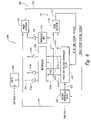
- FIG. 1is a logic diagram of a conventional phase detector circuit and charge pump.
- FIG. 2is a block diagram illustrating a phase detector including two phase detector circuits connected to a charge pump.
- FIG. 3is a logic diagram of the phase detector circuits of FIG. 2 in accordance with an embodiment of the present invention.
- FIG. 4is a timing diagram showing several of the waveforms present in the phase detector circuits.
- FIG. 5is a logic diagram of the charge pump of FIG. 2 in accordance with an embodiment of the present invention.
- FIG. 6is a block diagram of a clock generator circuit using an embodiment of the phase detector of FIG. 2 .
- FIG. 7is a block diagram of a computer system using a plurality of DRAMs, each of which includes the phase detector of FIG. 2 .
- the phase detectorincludes two single-to-dual signal converters 102 , 104 that receive input clock signals CLK 1 , CLK 2 , respectively, and produce complementary clock signals CLK 1 *, CLK 2 * and non-complementary clock signals CLK 1 , CLK 2 based on the original input clock signals.
- the single-to-dual signal convertersmay be implemented using a variety of designs known to one skilled in the art. For example, an inverter and transfer gate having the same propagation delay connected in parallel will produce a complementary and a non-complementary signal from an input clock signal.
- the CLK 1 , CLK 1 *, CLK 2 , CLK 2 * signalsare transmitted to two phase detector circuits 100 , 101 that produce select signals OUT 1 , OUT 1 *, OUT 2 , OUT 2 * and transmits them to a phase dependent signal source or a charge pump 200 via signal lines 106 , 107 , 108 , 109 , respectively.
- the charge pump 200in turn generates an output current IOUT according to the OUT 1 , OUT 1 * signals from the phase detector circuit 100 , and the OUT 2 , OUT 2 * signals from the phase detector circuit 101 .
- the IOUT currentmay be converted into a control signal V 0 by capacitor 20 connected to an output 280 , and the control signal V 0 may be used to adjust the delay value of a voltage controlled delay circuit.
- FIG. 3illustrates an embodiment of the phase detector circuits 100 , 101 in greater detail.
- Each detector circuit 100 , 101consists of two signal transition detectors 110 , 120 that generate a trigger pulse upon detecting a low-to-high transition of an input clock signal it receives.
- Each detector circuit 100 , 101also includes a dual output flip-flop 150 that is set and reset by the trigger pulses it receives from the signal transitions detectors 110 , 120 .
- Each flip-flop 150is formed by a pair of cross-coupled NAND gates 152 , 154 .
- the output from the phase detector circuits 100 , 101are applied to NAND gates 165 , 166 through inverters 161 - 164 .
- Each NAND gate 165 , 166also receives a respective input signal from the flip-flop 150 .
- the combination of inverters 161 - 164 and NAND gates 165 , 166creates a buffer circuit that will cause the respective NAND gates 165 , 166 to immediately switch upon receiving a trigger pulse from the respective signal transition detector, as explained below.
- Each phase detector circuit 100 , 101receives a pair of active-low control signals, SETA*, RSTA*, and SETB*, RSTB*, respectively.
- the SETA* and RSTA* signalsare applied to the phase detector circuit 100
- the SETB* and RSTB* signalsare applied to the phase detector circuit 101 .
- the control signalsare generated by a control circuit (not shown), and are used to put each phase detector circuit 100 , 101 into a predetermined state.
- Signal RSTA*is provided directly to the NAND gate 152 of the flip-flop 150 and the NAND gate 113 of the signal transition detector 120
- signal SETA*is provided directly to the NAND gate 154 of the flip-flop 150 and the NAND gate 113 of the signal transition detector 110 .
- the RSTB*, SETB* signalsare similarly provided to the respective NAND gates of the phase detector circuit 101 .
- phase detector circuit 100To illustrate the operation of the control signals, consider the effect the SETA*, RSTA* signals have on phase detector circuit 100 .
- the RSTA* and SETA* signalsare both high.
- the NAND gates 113 of the signal transition detectors 110 , 120behave as inverters, and the NAND gates 152 , 154 behave as simple two input NAND gates.
- the SETA* signalgoes low, the output of the NAND gates 113 a and 154 are forced high. Consequently, the NAND gate 118 a outputs a high to the NAND gate 152 , and the NAND gate 118 b outputs a low that sets the flip-flop 150 .
- Control signals RSTB* and SETB*operate in the same manner for the phase detector circuit 101 by forcing the OUT 2 , OUT 2 * signals to a predetermined state when active. To simplify the explanation of the operation of the signal transition detectors 110 , 120 , it will be assumed that the SETA*, RSTA*, SETB*, and RSTB* signals are inactive (i.e., at a high signal level).
- the CLK 1 , CLK 2 signalsare initially low thereby applying a low signal directly to one input of the NAND gates 118 b , 118 c and causing the inverters 116 a , 116 d to apply low signals to the other input of the NAND gates 118 a , 118 d , respectively.
- the NAND gates 118 a - dinitially output a high signal.
- the respective clock signalgoes high, e.g., the CLK 1 signal
- the NAND gate 118 coutputs a low signal until the high signal has propagated through inverter 112 c , NAND gate 113 c , and through series inverters 114 c , 115 c , 116 c .
- the inverter of 116 cthen applies a low signal to the NAND gate 118 c , thereby causing the output of the NAND gate 118 c to again go high.
- the signal transition detector 110outputs a low-going pulse responsive to the CLK 1 signal.
- the low-going pulsehas a width equal to the total propagation delay through inverter 112 , NAND gate 113 , and series inverters 114 , 115 , 116 .
- the signal transition detectors 110 , 120 in the phase detector circuit 100 , and the signal transition detector 120 in the phase detector circuit 101each operate in the same manner to output a low pulse responsive to the rising edge of the clock signal to which it is connected.
- each flip-flop 150sets or resets the flip-flops 150 . More specifically, each flip-flop 150 is set by each pulse from the respective signal transition detector 110 , thereby causing the NAND gate 152 to output a high signal and the NAND gate 154 to output a low signal. Each flip-flop 150 is reset by each pulse from the respective signal transition detector 120 , thereby causing the NAND gate 152 to output a low signal and NAND gate 154 to output a high signal.
- NAND gates 152 , 154are then inverted by NAND gates 165 , 166 , respectively, of the buffer circuit to provide the OUT 1 , OUT 1 *, OUT 2 , OUT 2 * signals to the charge pump 200 .
- the OUT 1 signalis high during the period between the rising edge of the CLK 2 signal and the falling edge of the CLK 1 signal (i.e., the rising edge of the CLK 1 * signal).
- the OUT 2 signal generated by the detector circuit 101is high during the period between the falling edge of the CLK 2 signal (i.e., the rising edge of the CLK 2 * signal) and the rising edge of the CLK 1 signal.
- phase detector circuits 100 , 101To illustrate the operation of the phase detector circuits 100 , 101 , consider three situations: first, where CLK 1 and CLK 2 are in phase; second, where CLK 1 is leading CLK 2 by ⁇ ; and third, where CLK 1 is lagging CLK 2 by ⁇ .
- FIG. 4 aThe phase relationship when the CLK 1 and CLK 2 signals are in phase is illustrated in FIG. 4 a .
- the OUT 1 signal from the phase detector circuit 100switches from low to high on the rising edge of the CLK 2 signal, and from high to low on the falling edge of the CLK 1 signal.
- the OUT 2 signal from the phase detector circuit 101switches from low to high on the falling edge of the CLK 2 signal, and from high to low on the rising edge of the CLK 1 signal. Since the CLK 1 signal is shown in FIG. 4 a as being in phase with the CLK 2 signal, the duty cycles of the OUT 1 and OUT 2 signals are both 50 percent, and the two signals will never be at the same logic level simultaneously.
- the OUT 1 , OUT 1 *, OUT 2 , OUT 2 * signalsare transmitted from the phase detector circuits 100 , 101 on signal lines 106 , 107 , 108 , 109 , respectively, to the input of a charge pump, such as a charge pump 200 , as shown in FIG. 5 .
- the charge pump 200includes a charging circuit 205 , a current source 270 , and a current sink 272 .
- the function of the charging circuit 205is to direct the current of the current source 270 and current sink 272 into, or out of the capacitor 20 ( FIG. 2 ), respectively, depending upon the relative duty cycles of the OUT 1 and OUT 2 signals.
- the resulting control signalmay have virtually no ripple when the phase detector 10 ( FIG. 2 ) is used in a voltage controlled delay circuit, as explained above.
- a clock signal generated using the voltage controlled delay circuithas significantly less phase jitter compared to a clock signal generated by a voltage controlled delay circuit using the phase detector of FIG. 1 .
- the charge pump 200includes transistors 245 - 248 on the left leg of the charging circuit 205 to form a compensation circuit 206 to compensate for current and voltage changes in a current driving circuit formed by transistors 243 , 244 , 249 , and 250 on the right leg of the charging circuit 205 .
- the compensation circuit 206is provided so that the voltage across the charging circuit 205 is relatively constant during operation, regardless of where the currents of the current source 270 and the current sink 272 are being directed.
- a voltage follower 260is connected between the output 280 of the charging circuit 205 and node 262 of the compensation circuit 206 .
- the voltage follower 260provides a current path from the current source 270 to ground when current from the current sink 272 is being directed out of the capacitor 20 .
- the voltage follower 260also provides a current path from the current sink 272 to the positive supply when current from the current source 270 is directed to the output 280 . As will be explained in greater detail below, both of these situations occur where the CLK 1 and CLK 2 signals are not in phase.
- the current through the charging circuit 205is through two PMOS transistors and two NMOS transistors when current is being directed into or out of the capacitor 20 , namely, the transistors 242 , 244 , 247 , 251 or the transistors 241 , 245 , 250 , 252 .
- the current through the charging circuit 205is also through two PMOS transistors and two NMOS transistors, namely, the transistors 242 , 243 , 248 , 251 or the transistors 241 , 246 , 249 , 252 .
- the operating points of the active transistorswill remain relatively constant, and any capacitive charge pumping on the internal nodes of the charging circuit 205 will be minimized. It will be appreciated by one ordinarily skilled in the art that the transistors of the charging circuit 205 must be scaled accordingly.
- the charging circuit 205directs the current provided by the current source 270 through the PMOS transistors 242 , 244 to charge the capacitor 20 (indicated in FIG. 4 b as “I+”).
- a path for the current from the current sink 272is provided through the voltage follower 260 and the NMOS transistors 247 , 251 .
- the charging circuit 205does not charge or discharge the capacitor 20 so the voltage on the capacitor 20 remains constant, as was previously explained (indicated in FIG. 4 b as 0 (A) or 0 (B)).
- the NMOS transistors 250 , 252provide a conductive path for the current sink 272 to sink current from the capacitor 20 (indicated in FIG. 4 c as “I ⁇ ”).
- a current path for the current of the current source 270is provided through the voltage follower 260 and the PMOS transistors 241 , 245 .
- the charging circuit 205does not charge or discharge the capacitor 20 so the voltage on the capacitor 20 remains constant (indicated in FIG. 4 c as 0 (A) or 0 (B)).
- any change in the control voltage V 0depends upon whether current is flowing into or out of the capacitor 20 , as explained above.
- OUT 1 and OUT 2never have the same logic level so no current flows either into or out of the capacitor 20 .
- OUT 1 and OUT 2are both high or both low for a portion of each cycle.
- FIG. 4 bwhen the CLK 1 signal leads the CLK 2 signal, OUT 1 and OUT 2 are low for more than 50 percent of each cycle so that OUT 1 and OUT 2 are both low for a portion of each cycle.
- phase detector 10may be modified to produce a control signal that adjust the CLK 1 and CLK 2 signals to have a 180 degrees phase relationship.
- the CLK 1 * and CLK 2 signalsare transmitted to nodes 95 , 96 of the phase detector circuit 100
- the CLK 1 and CLK 2 * signalsare transmitted to nodes 97 , 98 of the phase detector circuit 101 , resulting in a phase detector that generates a non-varying control signal when the CLK 1 and CLK 2 signals are in phase.
- the phase detector circuits 100 , 101transmit the OUT 1 , OUT 1 *, OUT 2 , OUT 2 * signals to the charge pump 200 so that the phase detector 10 generates a non-varying control signal when the CLK 1 and CLK 2 signals have a 180 degree phase relationship.
- the current source 270 and the current sink 272 of the charge pump 200may be of any current source circuit known in the art.
- a high-swing cascode current mirroras described in “CMOS Circuit Design, Layout, and Simulation,” published by IEEE Press, is used for both the current source 270 and the current sink 272 .
- the use of this particular current sourceis meant for illustrative purposes only, and is not intended to limit the scope of the present invention.
- the charge pump 200( FIG. 2 ) has been described with respect to the embodiment illustrated in FIG. 5 .
- an integrator circuit using an operational amplifiermay also be used for the charge pump 200 .
- Such an integrator circuitis formed by coupling a capacitor across the output of the operational amplifier and the inverting input.
- the OUT 1 and OUT 2 signals generated by the phase detector circuits 100 and 101are applied through two resistors of equal resistance to the non-inverting input of the operational amplifier, and the OUT 1 * and OUT 2 * signals are applied through two resistors of equal resistance to the inverting input.
- the resulting charge pumpwill generate increasing and decreasing control signals when the CLK 1 and CLK 2 signals are not in phase, and generate a control signal with virtually no ripple when the clock signals are in phase.
- FIG. 6Shown in FIG. 6 is a block diagram of a clock generator circuit that may be used in packetized DRAMs to provide a sequence of clock signals that have predetermined phases relative to a master clock signal.
- the clock generator circuitcontains a first delay-locked loop 301 and a second delay-locked loop 302 , each having a phase detector 10 of FIG. 2 .
- a multiplexer 330 having a plurality of output lines coupled to respective clock drivers 314 a - nmay be coupled to the first delay-lock loop 301 to couple one of the clock signals produced by the multi-tap voltage controlled delay circuit 310 to a clock output terminal 316 for use, for example, with a latch 340 to latch command data CMD DATA in packetized DRAM.
- the multiplexer 330couples the input of each of the clock drivers 314 a - n to any one of the clock signals produced by the multi-tap voltage controlled delay circuit 310 .
- the first delay-locked loopincludes a multi-tap voltage controlled delay circuit 310 and a first phase detector 10 a .
- the multi-tap voltage controlled delay circuit 310generates a sequence of clock signals on output lines 312 a - 312 n that are increasingly delayed from a first clock signal on line 312 a to a last clock signal on line 312 n .
- Two of the clock signals, preferably the first and last clock signals,are locked to each other using the delay-locked loop 301 so that they have a predetermined phase with respect to each other.
- the first clock signal on line 312 a and the last clock signal on line 312 nmay be locked so that they are the inverse of each other, that is, the predetermined phase relationship is 180 degrees from each other.
- the predetermined phase relationshipcould be 360 degrees so the first and last clock signals are in phase.
- the first phase detector 10 acompares the phase of the clock signals on lines 312 a and 312 n and generates the first control signal as a function of the phase difference therebetween.
- the first control signalis provided to the multi-tap voltage-controlled delay circuit 310 on line 311 to adjust the relative delay between the clock signal on line 312 a and line 312 n .
- the phase detector 10 awill continue to provide the first control signal until the first and last clock signals have obtained the predetermined phase relationship.
- the second delay-locked loop 302includes a second voltage controlled delay circuit 320 and a second phase detector 10 b .
- a second delay-locked looplocks a clock signal from the multi-tap voltage controlled circuit 310 to a master clock signal CMD CLK on line 305 so that the increasingly delayed clock signals of the multi-tap voltage controlled delay circuit 310 have phase delays with respect to the CMD CLK signal.
- the clock signal from the multi-tap voltage controlled circuit 310is provided to an input of the second phase detector 10 b through a simulated multiplexer 317 and a clock driver 318 .
- the relative phase delays of the simulated multiplexer 317 and the clock driver 318are nearly identical to that of the multiplexer 330 and the clock drivers 314 a - n . Consequently, the phase detector 10 b will receive a clock signal having the same relative phase delay as a clock signal output by the clock drivers 314 a - n.
- the second delay-lock loop 302may delay lock the first clock signal on line 312 a to the CMD CLK signal so that they have substantially the same phase, that is, the predetermined phase relationship is zero degrees from each other.
- the voltage controlled delay circuit 320receives the CMD CLK signal and generates a reference clock signal on line 322 having a delay relative to the CMD CLK signal that is a function of a second control signal on line 321 .
- the clock signal on line 322is provided to the multi-tap voltage controlled circuit 310 and used to generate the sequence of increasingly delayed clock signals 312 a - 312 n.
- the second phase detector 10 bcompares the phase of the CMD CLK signal to the phase of the first clock signal on line 312 a and generates a second control signal as a function of the difference therebetween.
- the clock signal provided to the phase detector 10 bis delayed through the simulated multiplexer 317 and the clock driver 318 approximately the same amount as the clock signals output by the clock drivers 314 a - n .
- the second control signalis used to adjust the delay value of the voltage controlled delay circuit 320 .
- the second control signalis provided by the second phase detector 10 b until the CMD CLK signal and the first clock signal from the multi-tap voltage controlled circuit 310 have obtained the predetermined phase relationship.
- the clock generator circuit of FIG. 6is described in greater detail in U.S.
- FIG. 7A computer system using the phase detector 10 of FIG. 2 in each of a plurality of packetized DRAMs 401 is shown in FIG. 7 .
- the computer system 400includes a processor 402 having a processor bus 404 coupled to three packetized dynamic random access memory or SLDRAMs 401 a - c .
- the computer system 400also includes one or more input devices 410 , such as a keypad or a mouse, coupled to the processor 402 through a bus bridge 412 and an expansion bus 414 , such as an industry standard architecture (“ISA”) bus or a Peripheral component interconnect (“PCI”) bus.
- ISAindustry standard architecture
- PCIPeripheral component interconnect
- One or more output devices 420are coupled to the processor 402 to display or otherwise output data generated by the processor 402 .
- the output devices 420are coupled to the processor 402 through the expansion bus 414 , bus bridge 412 and processor bus 404 . Examples of output devices 420 include printers and video display units.
- One or more data storage devices 422are coupled to the processor 402 through the processor bus 404 , bus bridge 412 , and expansion bus 414 to store data in or retrieve data from storage media (not shown). Examples of storage devices 422 and storage media include fixed disk drives floppy disk drives, tape cassettes and compact-disk read-only memory drives.
- the processor 402communicates with the memory devices 401 a - c via the processor bus 404 by sending the memory devices 401 a - c command packets that contain both control and address information.
- Datais coupled between the processor 402 and the memory devices 401 a - c , through a data bus portion of the processor bus 404 .
- all the memory devices 401 a - care coupled to the same conductors of the processor bus 404 , only one memory device 401 a - c at a time reads or writes data, thus avoiding bus contention on the processor bus 404 .
- Bus contentionis avoided by each of the memory devices 401 a - c and the bus bridge 412 having a unique identifier, and the command packet contains an identifying code that selects only one of these components.
- the computer system 400also includes a number of other components and signal lines which have been omitted from FIG. 7 in the interests of brevity.
- the memory devices 401 a - calso receive a command or master clock signal to provide internal timing signals, a data clock signal clocking data into and out of the memory device 401 a - c , and a FLAG signal signifying the start of a command packet.
- the signal transition detector circuits 110 , 120have been described as generating a negative trigger pulse upon detecting a transition of an input signal.
- the charge pump 200 shown in FIG. 5is described as generating a current output signal IOUT having a positive polarity when CLK 1 is leading CLK 2 , and having a negative polarity when CLK 1 is lagging CLK 2 .
- connection of the OUT 1 , OUT 1 *, OUT 2 , OUT 2 * signals to the transistors 241 - 252 of the charging circuit 205may be modified so that the IOUT signal will have a negative polarity when CLK 1 is leading CLK 2 , and have a positive polarity when CLK 1 is lagging CLK 2 . Accordingly, the invention is not limited except as by the appended claims.
Landscapes
- Physics & Mathematics (AREA)
- Nonlinear Science (AREA)
- Engineering & Computer Science (AREA)
- Power Engineering (AREA)
- Stabilization Of Oscillater, Synchronisation, Frequency Synthesizers (AREA)
- Dram (AREA)
Abstract
Description
This application is a continuation of U.S. patent application Ser. No. 10/186,471, filed Jun. 28, 2002, now U.S. Pat. No. 7,016,451 which is a continuation of U.S. patent application Ser. No. 09/260,212, filed Mar. 1, 1999, issued Oct. 22, 2002 as U.S. Pat. No. 6,470,060 B1.
This invention relates to generating a control signal and, more particularly, to generating a control signal based on the phase relationship between two input clock signals, and to memory devices and computer systems using such control signal generators.
Conventional computer systems include a processor (not shown) coupled to a variety of memory devices, including read-only memories (“ROMs”) which traditionally store instructions for the processor, and a system memory to which the processor may write data and from which the processor may read data. The processor may also communicate with an external cache memory, which is generally a static random access memory (“SRAM”). The processor also communicates with input devices, output devices, and data storage devices.
Processors generally operate at a relatively high speed. Processors such as the Pentium® and Pentium II® microprocessors are currently available that operate at clock speeds of at least 400 MHz. However, the remaining components of existing computer systems, with the exception of SRAM cache memory, are not capable of operating at the speed of the processor. For this reason, the system memory devices, as well as the input devices, output devices, and data storage devices, are not coupled directly to the processor bus. Instead, the system memory devices are generally coupled to the processor bus through a memory controller, bus bridge or similar device, and the input devices, output devices, and data storage devices are coupled to the processor bus through a bus bridge. The memory controller allows the system memory devices to operate at a clock frequency that is substantially lower than the clock frequency of the processor. Similarly, the bus bridge allows the input devices, output devices, and data storage devices to operate at a frequency that is substantially lower than the clock frequency of the processor. Currently, for example, a processor having a 300 MHz clock frequency may be mounted on a mother board having a 66 MHz clock frequency for controlling the system memory devices and other components.
Access to system memory is a frequent operation for the processor. The time required for the processor, operating, for example, at 300 MHz, to read data from or write data to a system memory device operating at, for example, 66 MHz, greatly slows the rate at which the processor is able to accomplish its operations. Thus, much effort has been devoted to increasing the operating speed of system memory devices.
System memory devices are generally dynamic random access memories (“DRAMs”). Initially, DRAMs were asynchronous and thus did not operate at even the clock speed of the motherboard. In fact, access to asynchronous DRAMs often required that wait states be generated to halt the processor until the DRAM had completed a memory transfer. However, the operating speed of asynchronous DRAMs was successfully increased through such innovations as burst and page mode DRAMs, which did not require that an address be provided to the DRAM for each memory access. More recently, synchronous dynamic random access memories (“SDRAMs”) have been developed to allow the pipelined transfer of data at the clock speed of the motherboard. However, even SDRAMs are typically incapable of operating at the clock speed of currently available processors. Thus, SDRAMs cannot be connected directly to the processor bus, but instead must interface with the processor bus through a memory controller, bus bridge, or similar device. The disparity between the operating speed of the processor and the operating speed of SDRAMs continues to limit the speed at which processors may complete operations requiring access to system memory.
A solution to this operating speed disparity has been proposed in the form of a packetized memory device known as a SLDRAM memory device. In the SLDRAM architecture, the system memory may be coupled to the processor, either directly through the processor bus or through a memory controller. Rather than requiring that separate address and control signals be provided to the system memory, SLDRAM memory devices receive command packets that include both control and address information. The SLDRAM memory device then outputs or receives data on a data bus that may be coupled directly to the data bus portion of the processor bus. A master clock signal transmitted to each memory device is used to synchronize data transfer between the processor and memory device and also serves as a basis from which to generate internal clock signals coordinating internal memory operations.
One of the factors limiting the access speed of SLDRAM memory devices is the speed at which the command buffer of each device can store and process the command packets. The processing speed of the command buffer is dependent on the control of the relative timing between transmission of the command packets from the processor and an internal clock signal ICLK of the memory device used to trigger a latch in the command buffer to capture the command signals. Both the command signals and the ICLK signal are delayed relative to receipt of the command packet on a command bus and a command clock signal CMDCLK. Furthermore, the amount of the delay is highly variable, and it is difficult to control. If the delay of the internal clock signal ICLK cannot be precisely controlled, it may cause the latch in the command buffer to latch invalid command signals. Thus, the speed at which command packets can be applied to the memory device is limited by the delays in the memory device. Similar problems exist for other control signals in the memory device that control the operation of the memory device during each clock cycle, such as latching of data in the memory device and in a memory controller.
Consequently, the operation of a SLDRAM memory architecture necessitates the generation of a sequence of clock signals having predetermined phases relative to a master clock signal. Phase-locked and delay locked loops have been employed to ensure the precise phase relationship between clock signals. In such a closed loop, there is typically a phase detector receiving two clock signals, and a voltage controlled delay circuit through which one clock signal passes. The voltage controlled delay circuit receives control signals from the phase detector that are used adjust the variable delay value in order to establish a predetermined phase relationship between the two clock signals. For example, where the desired phase relationship between two clock signals is zero degrees, the phase detector will detect any phase difference between the two clock signals and generate a control signal that is transmitted to the voltage controlled delay circuit. The delay circuit will adjust the delay value according to the control signal until the clock signal passing through the voltage controlled delay circuit is synchronized with the other clock signal. The clock control circuitry in an SLDRAM is described in greater detail in U.S. patent application Ser. Nos. 08/879,847, 08/890,055, 08/933,324, 08/994,461, 09/146,716, and 09/150,079, which are incorporated herein by reference.
A single phase detector connected to a CMOS inverter has been used as a means of providing a control signal to the above-described voltage controlled delay circuits. As shown inFIG. 1 , clock signals CLK1 and CLK2 are applied to twopulse generating circuits NAND gate 16 receiving a respective clock signal directly and through three series connectedinverters pulse generating circuit flop 26 formed bycross-coupled NAND gates flop 26 is connected to the gates of aninverter 36 formed by aPMOS transistor 38 and anNMOS transistor 40. Acurrent source 44 supplies current to the source of thePMOS transistor 38, and acurrent sink 46 draws current from the source of theNMOS transistor 40. When the output from the flip-flop 26 is low, thePMOS transistor 38 is turned ON and theNMOS transistor 40 is turned OFF. In this condition, a conductive path is created for thecurrent source 44 to couple current to acapacitor 48. A control signal VOUT is generated by thecapacitor 48. When thecurrent source 44 is applying current to thecapacitor 48, the voltage of the control signal VOUT increases linearly. In the alternative case where the output from the flip-flop 26 is high, thePMOS transistor 38 is switched OFF and theNMOS transistor 40 is switched ON. Thecurrent sink 46 is then coupled to thecapacitor 48 to draw current from thecapacitor 48. The voltage of the control signal VOUT then decreases linearly. As a result, the control signal VOUT has a sawtooth waveform component.
The problem with using a single phase detector connected to aninverter 36, as shown inFIG. 1 , is that even after the voltage controlled delay circuit has been adjusted so the clock signals have the predetermined phase relationship, the circuit will nevertheless continue to generate a sawtooth ripple voltage at its output. The sawtooth waveform component of the control signal VOUT is transmitted to the voltage controlled delay circuit (not shown inFIG. 1 ), which is forced to constantly adjust the delay value, and consequently, the phase relationship between the two clock signals CLK1 and CLK2. The closed loop system will oscillate around a center-point and continue to “hunt” for the optimum control voltage value.
The result is a “phase jitter” imparted to clock signals used to latch command and data signals. Although the phase jitter introduced by the sawtooth ripple voltage may be acceptable in some applications, in high speed memory applications where the clock frequencies are high and the need to control the phase relationship between clock signals is critical, the clocks signals may fail to correctly latch command and data signals.
To accommodate the problems associated with the sawtooth ripple, the memory system designer may relax the timing requirements of the memory system by slowing down the clock frequencies and reducing the operating speed of the memory device. However, this approach defeats the primary purpose of developing high speed memory systems. Therefore, there is a need for a phase detector that generates a control signal that does not vary when the input clock signals have been adjusted to a predetermined phase relationship.
In one aspect of the invention, a phase detector having a phase detector circuit and a current source is provided. The phase detector circuit is configured to generate first and second phase dependent signals indicative of the phase relationship of first and second input clock signals. The current source is coupled to the phase detector circuit and is configured to provide an output current having a first polarity, an output current having a second opposite polarity, or provide no output current in accordance with the first and second phase dependent signals from the phase detector circuit.
In another aspect of the invention, a phase detector having a phase detector circuit and an output circuit is provided. The phase detector circuit is configured to generate first and second phase dependent signals indicative of the phase relationship of first and second input clock signals and the an output circuit is configured to provide an output signal having an increasing magnitude, a decreasing magnitude, or a constant magnitude in accordance with the first and second phase dependent signals from the phase detector circuit.
In another aspect of the invention, a phase detector having a phase detector circuit and an output circuit is provided. The phase detector circuit has first and second input nodes to receive first and second clock signals and further has first and second output nodes. The phase detector circuit is configured to produce a first output signal at the first output node and produce a second output signal at the second output node. The first output signal has a duty cycle related to the phase relationship between a rising edge of the first and second clock signals and the second output node has a duty cycle related to the phase relationship between a falling edge of the first and second clock signals. The output circuit has first and second input nodes coupled to a respective output node of the phase detector circuit and further has an output. The output circuit is configured to provide an output signal having an increasing magnitude, an output signal having a decreasing magnitude, or an output signal having a constant magnitude according to the relative duty cycles of the first and second output signals.
An embodiment of aphase detector 10 in accordance with the present invention is illustrated inFIG. 2 . The phase detector includes two single-to-dual signal converters phase detector circuits charge pump 200 viasignal lines charge pump 200 in turn generates an output current IOUT according to the OUT1, OUT1* signals from thephase detector circuit 100, and the OUT2, OUT2* signals from thephase detector circuit 101. The IOUT current may be converted into a control signal V0bycapacitor 20 connected to anoutput 280, and the control signal V0may be used to adjust the delay value of a voltage controlled delay circuit.
Eachphase detector circuit phase detector circuit 100, and the SETB* and RSTB* signals are applied to thephase detector circuit 101. The control signals are generated by a control circuit (not shown), and are used to put eachphase detector circuit NAND gate 152 of the flip-flop 150 and the NAND gate113 of thesignal transition detector 120, and signal SETA* is provided directly to theNAND gate 154 of the flip-flop 150 and the NAND gate113 of thesignal transition detector 110. The RSTB*, SETB* signals are similarly provided to the respective NAND gates of thephase detector circuit 101.
To illustrate the operation of the control signals, consider the effect the SETA*, RSTA* signals have onphase detector circuit 100. During normal operation of thephase detector circuit 100, the RSTA* and SETA* signals are both high. In this situation, the NAND gates113 of thesignal transition detectors NAND gates NAND gates NAND gate 118aoutputs a high to theNAND gate 152, and theNAND gate 118boutputs a low that sets the flip-flop 150. The OUT1 signal is then forced high and the OUT1* signal is forced low. In a similar manner, when the RSTA* signal goes low, the flip-flop 150 is reset so that the OUT1 signal is forced low and the OUT1* signal is forced high. Control signals RSTB* and SETB* operate in the same manner for thephase detector circuit 101 by forcing the OUT2, OUT2* signals to a predetermined state when active. To simplify the explanation of the operation of thesignal transition detectors
In operation, the CLK1, CLK2 signals are initially low thereby applying a low signal directly to one input of theNAND gates inverters NAND gates NAND gate 118coutputs a low signal until the high signal has propagated throughinverter 112c,NAND gate 113c, and throughseries inverters 114c,115c,116c. The inverter of116cthen applies a low signal to theNAND gate 118c, thereby causing the output of theNAND gate 118cto again go high. Thus, thesignal transition detector 110 outputs a low-going pulse responsive to the CLK1 signal. The low-going pulse has a width equal to the total propagation delay through inverter112, NAND gate113, andseries inverters signal transition detectors phase detector circuit 100, and thesignal transition detector 120 in thephase detector circuit 101, each operate in the same manner to output a low pulse responsive to the rising edge of the clock signal to which it is connected.
The low-going pulse from each of thesignal transition detectors flops 150. More specifically, each flip-flop 150 is set by each pulse from the respectivesignal transition detector 110, thereby causing theNAND gate 152 to output a high signal and theNAND gate 154 to output a low signal. Each flip-flop 150 is reset by each pulse from the respectivesignal transition detector 120, thereby causing theNAND gate 152 to output a low signal andNAND gate 154 to output a high signal. The output ofNAND gates NAND gates charge pump 200. As a result, the OUT1 signal is high during the period between the rising edge of the CLK2 signal and the falling edge of the CLK1 signal (i.e., the rising edge of the CLK1* signal). In a similar manner, the OUT2 signal generated by thedetector circuit 101 is high during the period between the falling edge of the CLK2 signal (i.e., the rising edge of the CLK2* signal) and the rising edge of the CLK1 signal.
To illustrate the operation of thephase detector circuits
The phase relationship when the CLK1 and CLK2 signals are in phase is illustrated inFIG. 4 a. As explained above, the OUT1 signal from thephase detector circuit 100 switches from low to high on the rising edge of the CLK2 signal, and from high to low on the falling edge of the CLK1 signal. Also, the OUT2 signal from thephase detector circuit 101 switches from low to high on the falling edge of the CLK2 signal, and from high to low on the rising edge of the CLK1 signal. Since the CLK1 signal is shown inFIG. 4 aas being in phase with the CLK2 signal, the duty cycles of the OUT1 and OUT2 signals are both 50 percent, and the two signals will never be at the same logic level simultaneously.
Now consider the case where CLK1 is leading CLK2 by φ, as shown inFIG. 4 b. When CLK1 is leading CLK2 by φ, the OUT1 signal from thephase detector circuit 100 and the OUT2 signal from phase thedetector circuit 101 have duty cycles less than 50 percent, and may be at a low logic level simultaneously. Finally, consider the case where CLK1 is lagging CLK2 by φ, as shown inFIG. 4 c. When CLK1 is lagging CLK2 by φ, the resulting OUT1 and OUT2 signals fromphase detector circuits
The OUT1, OUT1*, OUT2, OUT2* signals are transmitted from thephase detector circuits signal lines charge pump 200, as shown inFIG. 5 . Thecharge pump 200 includes a chargingcircuit 205, acurrent source 270, and acurrent sink 272. The function of the chargingcircuit 205 is to direct the current of thecurrent source 270 andcurrent sink 272 into, or out of the capacitor20 (FIG. 2 ), respectively, depending upon the relative duty cycles of the OUT1 and OUT2 signals. Significantly, no current flows into or out of thecapacitor 20 when the CLK1 and CLK2 signals are in phase. Thus, the resulting control signal may have virtually no ripple when the phase detector10 (FIG. 2 ) is used in a voltage controlled delay circuit, as explained above. A clock signal generated using the voltage controlled delay circuit has significantly less phase jitter compared to a clock signal generated by a voltage controlled delay circuit using the phase detector ofFIG. 1 .
Thecharge pump 200 includes transistors245-248 on the left leg of the chargingcircuit 205 to form acompensation circuit 206 to compensate for current and voltage changes in a current driving circuit formed bytransistors circuit 205. Thecompensation circuit 206 is provided so that the voltage across the chargingcircuit 205 is relatively constant during operation, regardless of where the currents of thecurrent source 270 and thecurrent sink 272 are being directed.
Avoltage follower 260 is connected between theoutput 280 of the chargingcircuit 205 andnode 262 of thecompensation circuit 206. Thevoltage follower 260 provides a current path from thecurrent source 270 to ground when current from thecurrent sink 272 is being directed out of thecapacitor 20. Thevoltage follower 260 also provides a current path from thecurrent sink 272 to the positive supply when current from thecurrent source 270 is directed to theoutput 280. As will be explained in greater detail below, both of these situations occur where the CLK1 and CLK2 signals are not in phase. As a result, the current through the chargingcircuit 205 is through two PMOS transistors and two NMOS transistors when current is being directed into or out of thecapacitor 20, namely, thetransistors transistors capacitor 20, the current through the chargingcircuit 205 is also through two PMOS transistors and two NMOS transistors, namely, thetransistors transistors circuit 205 will be minimized. It will be appreciated by one ordinarily skilled in the art that the transistors of the chargingcircuit 205 must be scaled accordingly.
To illustrate the operation of thecharge pump 200 in conjunction with thephase detector circuits
As shown inFIG. 4 a, when OUT1 is low and OUT2 is high the current provided by thecurrent source 270 and sunk by thecurrent sink 272 bypasses theoutput 280 of the chargingcircuit 205 and simply flows through thetransistors FIG. 4 aas “0(A)”). Similarly, when OUT1 is high and OUT2 is low current flows from thecurrent source 270 to thecurrent sink 272 through thetransistors FIG. 4 aas “0(B)”). In either case, the chargingcircuit 205 does not charge or discharge thecapacitor 20 so the voltage on thecapacitor 20 remains constant.
As shown inFIG. 4 b, when both the OUT1 and OUT2 signals are low, the chargingcircuit 205 directs the current provided by thecurrent source 270 through thePMOS transistors FIG. 4 bas “I+”). A path for the current from thecurrent sink 272 is provided through thevoltage follower 260 and theNMOS transistors circuit 205 does not charge or discharge thecapacitor 20 so the voltage on thecapacitor 20 remains constant, as was previously explained (indicated inFIG. 4 bas0(A) or0(B)).
As shown inFIG. 4 c, when both the OUT1 and OUT2 signals are high, theNMOS transistors current sink 272 to sink current from the capacitor20 (indicated inFIG. 4 cas “I−”). A current path for the current of thecurrent source 270 is provided through thevoltage follower 260 and thePMOS transistors 241,245. As mentioned before, whenever the OUT1 and OUT2 signals are at different logic levels, the chargingcircuit 205 does not charge or discharge thecapacitor 20 so the voltage on thecapacitor 20 remains constant (indicated inFIG. 4 cas0(A) or0(B)).
Any change in the control voltage V0depends upon whether current is flowing into or out of thecapacitor 20, as explained above. When the CLK1 and CLK2 signals are in phase, as illustrated inFIG. 4 a, OUT1 and OUT2 never have the same logic level so no current flows either into or out of thecapacitor 20. In contrast, when the CLK1 signal and the CLK2 signal have different phases, OUT1 and OUT2 are both high or both low for a portion of each cycle. As illustrated inFIG. 4 b, when the CLK1 signal leads the CLK2 signal, OUT1 and OUT2 are low for more than 50 percent of each cycle so that OUT1 and OUT2 are both low for a portion of each cycle. As a result, as explained above, current flows into thecapacitor 20, thereby increasing the control voltage V0. Similarly, when the CLK1 signal lags the CLK2 signal as illustrated inFIG. 4 c, OUT1 and OUT2 are high for more than 50 percent of each cycle so that OUT1 and OUT2 are both high for a portion of each cycle. As a result, current flows out of thecapacitor 20, thereby decreasing the control voltage V0.
The discussion of thephase detector 10 has so far only considered the case where the CLK1 and CLK2 signals are adjusted so that they are approximately in phase. However, thephase detector 10 may be modified to produce a control signal that adjust the CLK1 and CLK2 signals to have a 180 degrees phase relationship. As shown inFIG. 3 , the CLK1* and CLK2 signals are transmitted tonodes phase detector circuit 100, while the CLK1 and CLK2* signals are transmitted tonodes phase detector circuit 101, resulting in a phase detector that generates a non-varying control signal when the CLK1 and CLK2 signals are in phase. However, when the CLK1 and CLK1* signals are reconnected to thenodes nodes phase detector circuits charge pump 200 so that thephase detector 10 generates a non-varying control signal when the CLK1 and CLK2 signals have a 180 degree phase relationship.
Thecurrent source 270 and thecurrent sink 272 of thecharge pump 200 may be of any current source circuit known in the art. In a preferred embodiment, a high-swing cascode current mirror, as described in “CMOS Circuit Design, Layout, and Simulation,” published by IEEE Press, is used for both thecurrent source 270 and thecurrent sink 272. The use of this particular current source is meant for illustrative purposes only, and is not intended to limit the scope of the present invention.
The charge pump200 (FIG. 2 ) has been described with respect to the embodiment illustrated inFIG. 5 . However, an integrator circuit using an operational amplifier may also be used for thecharge pump 200. Such an integrator circuit is formed by coupling a capacitor across the output of the operational amplifier and the inverting input. The OUT1 and OUT2 signals generated by thephase detector circuits
Shown inFIG. 6 is a block diagram of a clock generator circuit that may be used in packetized DRAMs to provide a sequence of clock signals that have predetermined phases relative to a master clock signal. The clock generator circuit contains a first delay-lockedloop 301 and a second delay-lockedloop 302, each having aphase detector 10 ofFIG. 2 . Amultiplexer 330 having a plurality of output lines coupled to respective clock drivers314a-nmay be coupled to the first delay-lock loop 301 to couple one of the clock signals produced by the multi-tap voltage controlleddelay circuit 310 to aclock output terminal 316 for use, for example, with alatch 340 to latch command data CMD DATA in packetized DRAM. Themultiplexer 330 couples the input of each of the clock drivers314a-nto any one of the clock signals produced by the multi-tap voltage controlleddelay circuit 310.
The first delay-locked loop includes a multi-tap voltage controlleddelay circuit 310 and afirst phase detector 10a. The multi-tap voltage controlleddelay circuit 310 generates a sequence of clock signals on output lines312a-312nthat are increasingly delayed from a first clock signal online 312ato a last clock signal online 312n. Two of the clock signals, preferably the first and last clock signals, are locked to each other using the delay-lockedloop 301 so that they have a predetermined phase with respect to each other. For example, the first clock signal online 312aand the last clock signal online 312nmay be locked so that they are the inverse of each other, that is, the predetermined phase relationship is 180 degrees from each other. Alternatively, the predetermined phase relationship could be 360 degrees so the first and last clock signals are in phase. Thefirst phase detector 10acompares the phase of the clock signals onlines delay circuit 310 online 311 to adjust the relative delay between the clock signal online 312aandline 312n. Thephase detector 10awill continue to provide the first control signal until the first and last clock signals have obtained the predetermined phase relationship.
Likewise, the second delay-lockedloop 302 includes a second voltage controlleddelay circuit 320 and asecond phase detector 10b. A second delay-locked loop locks a clock signal from the multi-tap voltage controlledcircuit 310 to a master clock signal CMD CLK online 305 so that the increasingly delayed clock signals of the multi-tap voltage controlleddelay circuit 310 have phase delays with respect to the CMD CLK signal. The clock signal from the multi-tap voltage controlledcircuit 310 is provided to an input of thesecond phase detector 10bthrough asimulated multiplexer 317 and aclock driver 318. The relative phase delays of thesimulated multiplexer 317 and theclock driver 318 are nearly identical to that of themultiplexer 330 and the clock drivers314a-n. Consequently, thephase detector 10bwill receive a clock signal having the same relative phase delay as a clock signal output by the clock drivers314a-n.
For example, the second delay-lock loop 302 may delay lock the first clock signal online 312ato the CMD CLK signal so that they have substantially the same phase, that is, the predetermined phase relationship is zero degrees from each other. The voltage controlleddelay circuit 320 receives the CMD CLK signal and generates a reference clock signal online 322 having a delay relative to the CMD CLK signal that is a function of a second control signal online 321. The clock signal online 322 is provided to the multi-tap voltage controlledcircuit 310 and used to generate the sequence of increasingly delayed clock signals312a-312n.
Thesecond phase detector 10bcompares the phase of the CMD CLK signal to the phase of the first clock signal online 312aand generates a second control signal as a function of the difference therebetween. The clock signal provided to thephase detector 10bis delayed through thesimulated multiplexer 317 and theclock driver 318 approximately the same amount as the clock signals output by the clock drivers314a-n. The second control signal is used to adjust the delay value of the voltage controlleddelay circuit 320. The second control signal is provided by thesecond phase detector 10buntil the CMD CLK signal and the first clock signal from the multi-tap voltage controlledcircuit 310 have obtained the predetermined phase relationship. The clock generator circuit ofFIG. 6 is described in greater detail in U.S. patent application Ser. No. 08/879,847, which, as mentioned above, has been incorporated herein by reference.
A computer system using thephase detector 10 ofFIG. 2 in each of a plurality of packetized DRAMs401 is shown inFIG. 7 . With reference toFIG. 7 thecomputer system 400 includes aprocessor 402 having aprocessor bus 404 coupled to three packetized dynamic random access memory or SLDRAMs401a-c. Thecomputer system 400 also includes one ormore input devices 410, such as a keypad or a mouse, coupled to theprocessor 402 through abus bridge 412 and anexpansion bus 414, such as an industry standard architecture (“ISA”) bus or a Peripheral component interconnect (“PCI”) bus. Theinput devices 410 allow an operator or an electronic device to input data to thecomputer system 400. One ormore output devices 420 are coupled to theprocessor 402 to display or otherwise output data generated by theprocessor 402. Theoutput devices 420 are coupled to theprocessor 402 through theexpansion bus 414,bus bridge 412 andprocessor bus 404. Examples ofoutput devices 420 include printers and video display units. One or moredata storage devices 422 are coupled to theprocessor 402 through theprocessor bus 404,bus bridge 412, andexpansion bus 414 to store data in or retrieve data from storage media (not shown). Examples ofstorage devices 422 and storage media include fixed disk drives floppy disk drives, tape cassettes and compact-disk read-only memory drives.
In operation, theprocessor 402 communicates with the memory devices401a-cvia theprocessor bus 404 by sending the memory devices401a-ccommand packets that contain both control and address information. Data is coupled between theprocessor 402 and the memory devices401a-c, through a data bus portion of theprocessor bus 404. Although all the memory devices401a-care coupled to the same conductors of theprocessor bus 404, only one memory device401a-cat a time reads or writes data, thus avoiding bus contention on theprocessor bus 404. Bus contention is avoided by each of the memory devices401a-cand thebus bridge 412 having a unique identifier, and the command packet contains an identifying code that selects only one of these components.
Thecomputer system 400 also includes a number of other components and signal lines which have been omitted fromFIG. 7 in the interests of brevity. For example, as explained above, the memory devices401a-calso receive a command or master clock signal to provide internal timing signals, a data clock signal clocking data into and out of the memory device401a-c, and a FLAG signal signifying the start of a command packet.
From the foregoing it will be appreciated that, although specific embodiments of the invention have been described herein for purposes of illustration, various modifications may be made without deviating from the spirit and scope of the invention. For example, the signaltransition detector circuits flop 150 allows the use of a signal transition detector that generates a positive trigger pulse. Also, thecharge pump 200 shown inFIG. 5 is described as generating a current output signal IOUT having a positive polarity when CLK1 is leading CLK2, and having a negative polarity when CLK1 is lagging CLK2. However, the connection of the OUT1, OUT1*, OUT2, OUT2* signals to the transistors241-252 of the chargingcircuit 205 may be modified so that the IOUT signal will have a negative polarity when CLK1 is leading CLK2, and have a positive polarity when CLK1 is lagging CLK2. Accordingly, the invention is not limited except as by the appended claims.
Claims (18)
1. A phase detector, comprising:
a first phase detector circuit having first and second clock signal transition detectors and a flip-flop, each clock signal transition detector having an input to receive a respective one of first and second input clock signals, the flip-flop having first and second inputs coupled to the output of a respective one of the clock signal transition detectors and further having an output corresponding to an output of the first phase detector;
a second phase detector circuit having first and second inputs to receive the first and second clock signals, respectively, and further having an output; and
an output circuit having first and second inputs coupled to the outputs of the first and second phase detector circuits and further having an output, the output circuit configured to provide an output current having a first polarity, an output current having a second opposite polarity, or no output current in response to output signals from the first and second phase detector circuits.
2. The phase detector ofclaim 1 wherein the second phase detector circuit comprises first and second clock signal transition detectors coupled to a respective input of the second phase detector circuit, and a flip flop coupled to the first and second clock signal transition detectors, the first phase detector circuit configured to generate an output signal having a duty cycle according to the phase relationship between a first clock edge of the first and second clock signals, and the second phase detector circuit configured to generate an output signal having a duty cycle according to the phase relationship between a second clock edge of the first and second clock signals.
3. The phase detector ofclaim 2 wherein the output circuit comprises:
a first current circuit;
a second current circuit; and
a switching circuit configured to selectively couple and decouple the output of the output circuit from the first and second current circuits responsive to the relative duty cycles of the output signals from the first and second phase detector circuits.
4. The phase detector ofclaim 3 wherein the output circuit provides a positive current in response to the output signal of the first phase detector circuit having a greater duty cycle than the output signal of the second phase detector circuit and a negative current in response to the output signal of the second phase detector circuit having a greater duty cycle than the output signal of the first phase detector circuit.
5. The phase detector ofclaim 1 , further comprising a capacitor coupled to the output of the output circuit.
6. A phase detector, comprising:
a phase detector circuit having first and second input nodes to receive first and second clock signals and further having first and second output nodes, the phase detector circuit configured to produce a first output signal at the first output node having a duty cycle related to the phase relationship between a rising edge of the first and second clock signals and produce a second output signal at the second output node having a duty cycle related to the phase relationship between a falling edge of the first and second clock signals, wherein the phase detector circuit comprises first and second circuits, each circuit including first and second transition detectors and a flip-flop coupled to the first and second transition detectors, each of the transition detectors having an input to receive a respective one of the first and second clock signals and configured to produce a respective trigger pulse provided to the flip-flop in response to a transition in the respective clock signal; and
an output circuit having first and second input nodes coupled to a respective output node of the phase detector circuit and further having an output, the output circuit configured to provide an output signal having an increasing magnitude, an output signal having a decreasing magnitude, or an output signal having a constant magnitude according to the relative duty cycles of the first and second output signals.
7. The phase detector ofclaim 6 wherein the output circuit comprises:
a first current circuit;
a second current circuit;
a switching circuit configured to selectively couple and decouple the output of the output circuit from the first and second current circuits responsive to the relative duty cycles of the first and second output signals; and
a capacitor coupled to the output of the output circuit.
8. The phase detector ofclaim 7 wherein the output circuit is configured to provide a positive current in response to the first output signal having a greater duty cycle than the second output signal and a negative current in response to the second output signal having a greater duty cycle than the first output signal.
9. A phase detector, comprising:
a phase detector circuit configured to generate first and second phase dependent signals indicative of the phase relationship of first and second input clock signals, the phase detector circuit comprising: first phase detector circuitry having first and second inputs to receive the first and second clock signals, respectively, and further having an output to provide a first phase dependent output signal; and second phase detector circuitry having first and second inputs to receive the first and second clock signals, respectively, and further having an output to provide a second phase dependent output signal; and
a current source coupled to the phase detector circuit and configured to provide an output current having a first polarity, an output current having a second opposite polarity, or provide no output current in accordance with the first and second phase dependent signals from the phase detector circuit.
10. The phase detector ofclaim 9 wherein the first phase detector circuitry comprises:
first and second clock signal transition detectors, each clock signal transition detector having an input to receive a respective one of first and second input clock signals and configured to produce a trigger pulse at an output in response to a transition in the respective clock signal; and
a flip-flop having first and second inputs coupled to the output of a respective one of the clock signal transition detectors and further having an output corresponding to an output of the first phase detector circuitry.
11. The phase detector ofclaim 9 wherein the first phase detector circuitry is configured to generate the first phase dependent output signal having a duty cycle related to the phase relationship between a rising edge of the first and second input clock signals and the second phase detector circuitry is configured to generate the second phase dependent output signal having a duty cycle related to the phase relationship between a falling edge of the first and second clock signals.
12. The phase detector ofclaim 11 wherein the current source comprises:
a first current circuit;
a second current circuit; and
a switching circuit configured to selectively couple and decouple an output of the current source from the first and second current circuits responsive to first and second phase dependent output signals.
13. The phase detector ofclaim 12 wherein the current source is configured to provide a positive current in response to the first phase dependent output signal having a greater duty cycle than the second phase dependent output signal and a negative current in response to the second phase dependent output signal having a greater duty cycle than the first phase dependent output signal.
14. The phase detector ofclaim 13 , further comprising a capacitor coupled to the output of the current source.
15. A phase detector, comprising:
a phase detector circuit configured to generate first and second phase dependent signals indicative of the phase relationship of first and second input clock signals; the phase detector circuit comprising: first phase detector circuitry having first and second inputs to receive the first and second clock signals, respectively, and further having an output to provide a first phase dependent output signal; and second phase detector circuitry having first and second inputs to receive the first and second clock signals, respectively, and further having an output to provide a second phase dependent output signal; and
an output circuit coupled to the phase detector circuit and configured to provide an output signal having an increasing magnitude, a decreasing magnitude, or a constant magnitude in accordance with the first and second phase dependent signals from the phase detector circuit.
16. The phase detector ofclaim 15 wherein the first phase detector circuitry is configured to generate the first phase dependent output signal having a duty cycle related to the phase relationship between a rising edge of the first and second input clock signals and the second phase detector circuitry is configured to generate the second phase dependent output signal having a duty cycle related to the phase relationship between a falling edge of the first and second clock signals.
17. The phase detector ofclaim 15 wherein the output circuit comprises:
a first current circuit;
a second current circuit;
a switching circuit configured to selectively couple and decouple the output of the output circuit from the first and second current circuits responsive to the relative duty cycles of the first and second output signals; and
a capacitor coupled to the output of the output circuit.
18. The phase detector ofclaim 17 wherein the output circuit is configured to provide a positive current in response to the first output signal having a greater duty cycle than the second output signal and a negative current in response to the second output signal having a greater duty cycle than the first output signal.
Priority Applications (4)
| Application Number | Priority Date | Filing Date | Title |
|---|---|---|---|
| US11/203,511US7418071B2 (en) | 1999-03-01 | 2005-08-12 | Method and apparatus for generating a phase dependent control signal |
| US12/178,442US7602876B2 (en) | 1999-03-01 | 2008-07-23 | Method and apparatus for generating a phase dependent control signal |
| US12/562,709US8107580B2 (en) | 1999-03-01 | 2009-09-18 | Method and apparatus for generating a phase dependent control signal |
| US13/354,702US8433023B2 (en) | 1999-03-01 | 2012-01-20 | Method and apparatus for generating a phase dependent control signal |
Applications Claiming Priority (3)
| Application Number | Priority Date | Filing Date | Title |
|---|---|---|---|
| US09/260,212US6470060B1 (en) | 1999-03-01 | 1999-03-01 | Method and apparatus for generating a phase dependent control signal |
| US10/186,471US7016451B2 (en) | 1999-03-01 | 2002-06-28 | Method and apparatus for generating a phase dependent control signal |
| US11/203,511US7418071B2 (en) | 1999-03-01 | 2005-08-12 | Method and apparatus for generating a phase dependent control signal |
Related Parent Applications (1)
| Application Number | Title | Priority Date | Filing Date |
|---|---|---|---|
| US10/186,471ContinuationUS7016451B2 (en) | 1999-03-01 | 2002-06-28 | Method and apparatus for generating a phase dependent control signal |
Related Child Applications (1)
| Application Number | Title | Priority Date | Filing Date |
|---|---|---|---|
| US12/178,442ContinuationUS7602876B2 (en) | 1999-03-01 | 2008-07-23 | Method and apparatus for generating a phase dependent control signal |
Publications (2)
| Publication Number | Publication Date |
|---|---|
| US20050286505A1 US20050286505A1 (en) | 2005-12-29 |
| US7418071B2true US7418071B2 (en) | 2008-08-26 |
Family
ID=22988239
Family Applications (8)
| Application Number | Title | Priority Date | Filing Date |
|---|---|---|---|
| US09/260,212Expired - LifetimeUS6470060B1 (en) | 1999-03-01 | 1999-03-01 | Method and apparatus for generating a phase dependent control signal |
| US09/991,198Expired - Fee RelatedUS6952462B2 (en) | 1999-03-01 | 2001-11-20 | Method and apparatus for generating a phase dependent control signal |
| US10/176,852Expired - Fee RelatedUS6931086B2 (en) | 1999-03-01 | 2002-06-20 | Method and apparatus for generating a phase dependent control signal |
| US10/186,471Expired - Fee RelatedUS7016451B2 (en) | 1999-03-01 | 2002-06-28 | Method and apparatus for generating a phase dependent control signal |
| US11/203,511Expired - Fee RelatedUS7418071B2 (en) | 1999-03-01 | 2005-08-12 | Method and apparatus for generating a phase dependent control signal |
| US12/178,442Expired - Fee RelatedUS7602876B2 (en) | 1999-03-01 | 2008-07-23 | Method and apparatus for generating a phase dependent control signal |
| US12/562,709Expired - Fee RelatedUS8107580B2 (en) | 1999-03-01 | 2009-09-18 | Method and apparatus for generating a phase dependent control signal |
| US13/354,702Expired - Fee RelatedUS8433023B2 (en) | 1999-03-01 | 2012-01-20 | Method and apparatus for generating a phase dependent control signal |
Family Applications Before (4)
| Application Number | Title | Priority Date | Filing Date |
|---|---|---|---|
| US09/260,212Expired - LifetimeUS6470060B1 (en) | 1999-03-01 | 1999-03-01 | Method and apparatus for generating a phase dependent control signal |
| US09/991,198Expired - Fee RelatedUS6952462B2 (en) | 1999-03-01 | 2001-11-20 | Method and apparatus for generating a phase dependent control signal |
| US10/176,852Expired - Fee RelatedUS6931086B2 (en) | 1999-03-01 | 2002-06-20 | Method and apparatus for generating a phase dependent control signal |
| US10/186,471Expired - Fee RelatedUS7016451B2 (en) | 1999-03-01 | 2002-06-28 | Method and apparatus for generating a phase dependent control signal |
Family Applications After (3)
| Application Number | Title | Priority Date | Filing Date |
|---|---|---|---|
| US12/178,442Expired - Fee RelatedUS7602876B2 (en) | 1999-03-01 | 2008-07-23 | Method and apparatus for generating a phase dependent control signal |
| US12/562,709Expired - Fee RelatedUS8107580B2 (en) | 1999-03-01 | 2009-09-18 | Method and apparatus for generating a phase dependent control signal |
| US13/354,702Expired - Fee RelatedUS8433023B2 (en) | 1999-03-01 | 2012-01-20 | Method and apparatus for generating a phase dependent control signal |
Country Status (1)
| Country | Link |
|---|---|
| US (8) | US6470060B1 (en) |
Cited By (7)
| Publication number | Priority date | Publication date | Assignee | Title |
|---|---|---|---|---|
| US20070241824A1 (en)* | 2006-03-30 | 2007-10-18 | Chien-Chung Tseng | Method and apparatus for generating output signal |
| US7554607B2 (en)* | 2005-09-20 | 2009-06-30 | National Semiconductor Corporation | Video signal detection circuit |
| US7629816B1 (en)* | 2005-12-21 | 2009-12-08 | Integrated Device Technology, Inc. | Method and apparatus for pre-clocking |
| US20100007383A1 (en)* | 1999-03-01 | 2010-01-14 | Harrison Ronnie M | Method and apparatus for generating a phase dependent control signal |
| US7954031B2 (en) | 1998-09-03 | 2011-05-31 | Round Rock Research, Llc | Method and apparatus for generating expect data from a captured bit pattern, and memory device using same |
| US20110199152A1 (en)* | 2010-02-17 | 2011-08-18 | Taiwan Semiconductor Manufacturing Company, Ltd. | Integrated circuits including a charge pump circuit and operating methods thereof |
| US9082506B2 (en) | 2013-03-13 | 2015-07-14 | Samsung Electronics Co., Ltd. | Synchronous semiconductor memory device having delay locked loop circuit and method of controlling the delay locked loop circuit |
Families Citing this family (68)
| Publication number | Priority date | Publication date | Assignee | Title |
|---|---|---|---|---|
| US5796673A (en)* | 1994-10-06 | 1998-08-18 | Mosaid Technologies Incorporated | Delay locked loop implementation in a synchronous dynamic random access memory |
| US6173432B1 (en)* | 1997-06-20 | 2001-01-09 | Micron Technology, Inc. | Method and apparatus for generating a sequence of clock signals |
| US6643787B1 (en)* | 1999-10-19 | 2003-11-04 | Rambus Inc. | Bus system optimization |
| US6725390B1 (en)* | 2000-06-29 | 2004-04-20 | Intel Corporation | Method and an apparatus for adjusting clock signal to sample data |
| EP1211811A1 (en)* | 2000-11-28 | 2002-06-05 | Koninklijke Philips Electronics N.V. | Fast frequency comparing circuit |
| US8385476B2 (en)* | 2001-04-25 | 2013-02-26 | Texas Instruments Incorporated | Digital phase locked loop |
| JP3502618B2 (en)* | 2001-07-19 | 2004-03-02 | 松下電器産業株式会社 | Phase-locked loop circuit and data reproducing apparatus |
| US6850107B2 (en) | 2001-08-29 | 2005-02-01 | Micron Technology, Inc. | Variable delay circuit and method, and delay locked loop, memory device and computer system using same |
| US6985025B1 (en)* | 2002-01-19 | 2006-01-10 | National Semiconductor Corporation | System for adjusting a power supply level of a digital processing component and method of operating the same |
| US6759881B2 (en) | 2002-03-22 | 2004-07-06 | Rambus Inc. | System with phase jumping locked loop circuit |
| US6911853B2 (en)* | 2002-03-22 | 2005-06-28 | Rambus Inc. | Locked loop with dual rail regulation |
| US6952123B2 (en)* | 2002-03-22 | 2005-10-04 | Rambus Inc. | System with dual rail regulated locked loop |
| US7135903B2 (en)* | 2002-09-03 | 2006-11-14 | Rambus Inc. | Phase jumping locked loop circuit |
| US6922091B2 (en)* | 2002-09-03 | 2005-07-26 | Rambus Inc. | Locked loop circuit with clock hold function |
| DE10214304B4 (en)* | 2002-03-28 | 2004-10-21 | Infineon Technologies Ag | Method and device for generating two signals with a predetermined distance between corresponding signal edges |
| EP1361655A1 (en)* | 2002-05-07 | 2003-11-12 | Semiconductor Ideas to The Market (ItoM) BV | Mirror suppression circuit in a quadrature demodulator |
| KR100486261B1 (en)* | 2002-09-16 | 2005-05-03 | 삼성전자주식회사 | Skew Free Dual Rail Bus Driver |
| US7020793B1 (en)* | 2003-01-31 | 2006-03-28 | Lsi Logic Corporation | Circuit for aligning signal with reference signal |
| US6829548B2 (en)* | 2003-04-03 | 2004-12-07 | Sun Microsystems, Inc. | DLL static phase error measurement technique |
| US7489757B2 (en)* | 2003-05-01 | 2009-02-10 | Mitsubishi Denki Kabushiki Kaisha | Clock data recovery circuit |
| US7168027B2 (en)* | 2003-06-12 | 2007-01-23 | Micron Technology, Inc. | Dynamic synchronization of data capture on an optical or other high speed communications link |
| KR100542696B1 (en)* | 2003-11-13 | 2006-01-11 | 주식회사 하이닉스반도체 | Repair fuse box of semiconductor device |
| KR100514414B1 (en)* | 2003-11-20 | 2005-09-09 | 주식회사 하이닉스반도체 | Delay locked loop |
| KR100567532B1 (en)* | 2003-12-10 | 2006-04-03 | 주식회사 하이닉스반도체 | Pulse width control circuit and its method |
| US8457152B2 (en)* | 2004-07-16 | 2013-06-04 | Qualcomm Incorporated | Multiple modulation schemes in single rate layering wireless communication systems |
| US7180370B2 (en)* | 2004-09-01 | 2007-02-20 | Micron Technology, Inc. | CMOS amplifiers with frequency compensating capacitors |
| WO2006083324A1 (en) | 2005-02-02 | 2006-08-10 | Lin Wen T | A system and method of detecting a phase, a frequency and an arrival-time difference between signals |
| US7549092B2 (en)* | 2005-09-29 | 2009-06-16 | Hynix Semiconductor, Inc. | Output controller with test unit |
| KR100738960B1 (en)* | 2006-02-22 | 2007-07-12 | 주식회사 하이닉스반도체 | Phase locked loop and control method of the same |
| US7671644B2 (en) | 2006-05-24 | 2010-03-02 | Micron Technology Inc. | Process insensitive delay line |
| TW200816644A (en)* | 2006-09-27 | 2008-04-01 | Nat Univ Chung Cheng | A phase detector |
| KR100834393B1 (en)* | 2006-10-31 | 2008-06-04 | 주식회사 하이닉스반도체 | Clock data recovery device. |
| US7459949B2 (en)* | 2007-01-30 | 2008-12-02 | Mosaid Technologies Incorporated | Phase detector circuit and method therefor |
| US7551012B2 (en)* | 2007-03-27 | 2009-06-23 | Mosaid Technologies Incorporated | Phase shifting in DLL/PLL |
| JP5153789B2 (en)* | 2007-01-30 | 2013-02-27 | モサイド・テクノロジーズ・インコーポレーテッド | Phase shift processing in delay locked loop / phase locked loop |
| US7746134B1 (en) | 2007-04-18 | 2010-06-29 | Altera Corporation | Digitally controlled delay-locked loops |
| US8363772B2 (en)* | 2007-05-29 | 2013-01-29 | Taiwan Semiconductor Manufacturing Company, Ltd. | Methods for eliminating phase distortion in signals |
| JP4619415B2 (en)* | 2008-01-09 | 2011-01-26 | 株式会社リコー | Oscillation frequency control circuit, DC-DC converter having the oscillation frequency control circuit, and semiconductor device |
| FR2940555B1 (en)* | 2008-12-19 | 2012-09-07 | Thales Sa | SELF-CALIBRATION FILTRATION DEVICE |
| JP2011050004A (en)* | 2009-08-28 | 2011-03-10 | Elpida Memory Inc | Semiconductor device and phase detection circuit |
| JP5433432B2 (en)* | 2010-01-18 | 2014-03-05 | 株式会社日立製作所 | Phase frequency comparator and serial transmission device |
| KR101103070B1 (en) | 2010-04-30 | 2012-01-06 | 주식회사 하이닉스반도체 | Clock Signal Duty Correction Circuit |
| US9143140B2 (en) | 2011-02-15 | 2015-09-22 | Cavium, Inc. | Multi-function delay locked loop |
| KR101933645B1 (en) | 2011-08-31 | 2018-12-31 | 삼성전자주식회사 | Phase change memory device, method of generating operation voltage of the same and memory system having the same |
| US8718216B2 (en)* | 2011-09-23 | 2014-05-06 | International Business Machines Corporation | Digital phase detector with zero phase offset |
| US8933679B2 (en)* | 2011-12-07 | 2015-01-13 | Maxim Integrated Products, Inc. | Adaptive dead-time control |
| JP2013258895A (en)* | 2012-05-18 | 2013-12-26 | Semiconductor Energy Lab Co Ltd | Semiconductor device and method for driving the same |
| US8825978B2 (en)* | 2012-06-04 | 2014-09-02 | Macronix International Co., Ltd. | Memory apparatus |
| ITTO20130347A1 (en)* | 2013-04-29 | 2014-10-30 | St Microelectronics Srl | CIRCUIT AND CALIBRATION METHOD FOR A DIGITALLY CONTROLLED OSCILLATOR |
| US9281034B2 (en) | 2013-10-03 | 2016-03-08 | Cavium, Inc. | Data strobe generation |
| JP6478562B2 (en) | 2013-11-07 | 2019-03-06 | 株式会社半導体エネルギー研究所 | Semiconductor device |
| US8929467B1 (en)* | 2014-01-13 | 2015-01-06 | Liming Xiu | Circuits and methods for one-wire communication bus of using pulse-edge for clock and pulse-duty-cycle for data |
| KR102253204B1 (en)* | 2014-02-07 | 2021-05-20 | 가부시키가이샤 한도오따이 에네루기 켄큐쇼 | Device |
| US9577525B2 (en) | 2014-03-04 | 2017-02-21 | Maxim Integrated Products, Inc. | Adaptive dead time control |
| US9590499B2 (en)* | 2014-07-18 | 2017-03-07 | Semiconductor Components Industries, Llc | Drive circuit and method |
| US9601181B2 (en)* | 2014-11-14 | 2017-03-21 | Cavium, Inc. | Controlled multi-step de-alignment of clocks |
| US9613679B2 (en)* | 2014-11-14 | 2017-04-04 | Cavium, Inc. | Controlled dynamic de-alignment of clocks |
| US9571263B2 (en)* | 2015-06-02 | 2017-02-14 | Avago Technologies General Ip (Singapore) Pte. Ltd. | Integrated circuit incorporating a low power data retiming circuit |
| US9865317B2 (en)* | 2016-04-26 | 2018-01-09 | Micron Technology, Inc. | Methods and apparatuses including command delay adjustment circuit |
| US9997220B2 (en) | 2016-08-22 | 2018-06-12 | Micron Technology, Inc. | Apparatuses and methods for adjusting delay of command signal path |
| US10177949B2 (en)* | 2016-08-30 | 2019-01-08 | The United States Of America As Represented By The Secretary Of The Air Force | Coherent phase-synchronizing circuit |
| KR102355437B1 (en) | 2017-05-11 | 2022-01-26 | 에스케이하이닉스 주식회사 | Semiconductor apparatus including clock generation circuit and semiconductor system |
| US10224938B2 (en) | 2017-07-26 | 2019-03-05 | Micron Technology, Inc. | Apparatuses and methods for indirectly detecting phase variations |
| US10340897B2 (en)* | 2017-07-28 | 2019-07-02 | Taiwan Semiconductor Manufacturing Company, Ltd. | Clock generating circuit and method of operating the same |
| JP2019039673A (en)* | 2017-08-22 | 2019-03-14 | セイコーエプソン株式会社 | Time digital conversion circuit, circuit device, physical quantity measuring device, electronic device, and moving object |
| US11206026B2 (en) | 2019-09-06 | 2021-12-21 | SK Hynix Inc. | Delay line, a delay locked loop circuit and a semiconductor apparatus using the delay line and the delay locked loop circuit |
| US11750201B2 (en)* | 2019-09-06 | 2023-09-05 | SK Hynix Inc. | Delay line, a delay locked loop circuit and a semiconductor apparatus using the delay line and the delay locked loop circuit |
| KR102832205B1 (en)* | 2020-04-10 | 2025-07-10 | 삼성전자주식회사 | Semiconductor device |
Citations (282)
| Publication number | Priority date | Publication date | Assignee | Title |
|---|---|---|---|---|
| US3633174A (en) | 1970-04-14 | 1972-01-04 | Us Navy | Memory system having self-adjusting strobe timing |
| US4004100A (en) | 1974-08-14 | 1977-01-18 | Nippon Electric Company, Ltd. | Group frame synchronization system |
| US4077016A (en) | 1977-02-22 | 1978-02-28 | Ncr Corporation | Apparatus and method for inhibiting false locking of a phase-locked loop |
| US4096402A (en) | 1975-12-29 | 1978-06-20 | Mostek Corporation | MOSFET buffer for TTL logic input and method of operation |
| US4404474A (en) | 1981-02-06 | 1983-09-13 | Rca Corporation | Active load pulse generating circuit |
| US4481625A (en) | 1981-10-21 | 1984-11-06 | Elxsi | High speed data bus system |
| US4508983A (en) | 1983-02-10 | 1985-04-02 | Motorola, Inc. | MOS Analog switch driven by complementary, minimally skewed clock signals |
| US4511846A (en) | 1982-05-24 | 1985-04-16 | Fairchild Camera And Instrument Corporation | Deskewing time-critical signals in automatic test equipment |
| US4514647A (en) | 1983-08-01 | 1985-04-30 | At&T Bell Laboratories | Chipset synchronization arrangement |
| US4524448A (en) | 1979-11-09 | 1985-06-18 | Nixdorf Computer Ag | Variable delay unit for data synchronizer using phase-sensitive counter to vary the delay |
| EP0171720A2 (en) | 1984-08-07 | 1986-02-19 | Kabushiki Kaisha Toshiba | Data delay/memory circuit |
| US4573017A (en) | 1984-01-03 | 1986-02-25 | Motorola, Inc. | Unitary phase and frequency adjust network for a multiple frequency digital phase locked loop |
| US4600895A (en) | 1985-04-26 | 1986-07-15 | Minnesota Mining And Manufacturing Company | Precision phase synchronization of free-running oscillator output signal to reference signal |
| US4603320A (en) | 1983-04-13 | 1986-07-29 | Anico Research, Ltd. Inc. | Connector interface |
| US4638187A (en) | 1985-10-01 | 1987-01-20 | Vtc Incorporated | CMOS output buffer providing high drive current with minimum output signal distortion |
| US4638451A (en) | 1983-05-03 | 1987-01-20 | Texas Instruments Incorporated | Microprocessor system with programmable interface |
| US4687951A (en) | 1984-10-29 | 1987-08-18 | Texas Instruments Incorporated | Fuse link for varying chip operating parameters |
| US4697167A (en) | 1983-09-19 | 1987-09-29 | Storage Technology Corporation | Sync pattern encoding system for data sectors written on a storage medium |
| US4727541A (en) | 1984-12-06 | 1988-02-23 | Fujitsu Limited | Hierarchical data transmission system |
| US4740962A (en) | 1985-12-23 | 1988-04-26 | Motorola, Inc. | Synchronizer for time division multiplexed data |
| US4746996A (en) | 1984-06-26 | 1988-05-24 | Hitachi, Ltd. | Skew error correction circuit for video signal reproducing apparatus |
| US4773085A (en) | 1987-06-12 | 1988-09-20 | Bell Communications Research, Inc. | Phase and frequency detector circuits |
| US4789796A (en) | 1985-12-23 | 1988-12-06 | U.S. Philips Corporation | Output buffer having sequentially-switched output |
| US4791622A (en) | 1983-09-19 | 1988-12-13 | Storage Technology Partners 11 | Optical data format employing resynchronizable data sectors |
| EP0295515A1 (en) | 1987-06-05 | 1988-12-21 | Anritsu Corporation | Signal generating apparatus |
| US4818995A (en) | 1986-05-19 | 1989-04-04 | Hitachi Ltd. | Parallel transmission system |
| US4893087A (en) | 1988-01-07 | 1990-01-09 | Motorola, Inc. | Low voltage and low power frequency synthesizer |
| US4902986A (en) | 1989-01-30 | 1990-02-20 | Asix Systems Corporation | Phased locked loop to provide precise frequency and phase tracking of two signals |
| US4924516A (en) | 1989-05-23 | 1990-05-08 | At&T Paradyne | Method and system for a synchronized pseudo-random privacy modem |
| US4953128A (en) | 1986-12-16 | 1990-08-28 | Mitsubishi Denki Kabushiki Kaisha | Variable delay circuit for delaying input data |
| JPH02112317U (en) | 1989-02-27 | 1990-09-07 | ||
| US4958088A (en) | 1989-06-19 | 1990-09-18 | Micron Technology, Inc. | Low power three-stage CMOS input buffer with controlled switching |
| US4972470A (en) | 1987-08-06 | 1990-11-20 | Steven Farago | Programmable connector |
| US4979185A (en) | 1989-10-30 | 1990-12-18 | Texas Instruments Incorporated | High speed serial data link |
| US4984204A (en) | 1988-01-28 | 1991-01-08 | Hitachi, Ltd. | High speed sensor system using a level shift circuit |
| US4984255A (en) | 1989-11-15 | 1991-01-08 | National Semiconductor Corporation | Edge transition insensitive delay line system and method |
| EP0406786A1 (en) | 1989-07-04 | 1991-01-09 | ALCATEL ITALIA S.p.A. | Device for transforming a type "D" flip-flop into a flip-flop called type "B" able to sample data both on leading and trailing edges of the clock signal |
| US5020023A (en) | 1989-02-23 | 1991-05-28 | International Business Machines Corporation | Automatic vernier synchronization of skewed data streams |
| US5038115A (en) | 1990-05-29 | 1991-08-06 | Myers Glen A | Method and apparatus for frequency independent phase tracking of input signals in receiving systems and the like |
| EP0450871A2 (en) | 1990-03-30 | 1991-10-09 | Xerox Corporation | Interfaces for transmission lines |
| US5062082A (en) | 1990-09-04 | 1991-10-29 | Samsung Electronics Co., Ltd. | Semiconductor memory device with delay in address predecoder circuit independent from ATD |
| US5075569A (en) | 1989-03-17 | 1991-12-24 | Tektronix, Inc. | Output device circuit and method to minimize impedance fluctuations during crossover |
| US5086500A (en) | 1987-08-07 | 1992-02-04 | Tektronix, Inc. | Synchronized system by adjusting independently clock signals arriving at a plurality of integrated circuits |
| US5087828A (en) | 1990-02-14 | 1992-02-11 | Daiichi Denshi Kogyo Kabushiki Kaisha | Timing circuit for single line serial data |
| JPH04135311A (en) | 1990-09-27 | 1992-05-08 | Nec Corp | Semiconductor integrated circuit |
| US5113519A (en) | 1989-05-15 | 1992-05-12 | International Business Machines Corporation | Maintenance of file attributes in a distributed data processing system |
| US5120990A (en) | 1990-06-29 | 1992-06-09 | Analog Devices, Inc. | Apparatus for generating multiple phase clock signals and phase detector therefor |
| US5122690A (en) | 1990-10-16 | 1992-06-16 | General Electric Company | Interface circuits including driver circuits with switching noise reduction |
| US5128560A (en) | 1991-03-22 | 1992-07-07 | Micron Technology, Inc. | Boosted supply output driver circuit for driving an all N-channel output stage |
| US5128563A (en) | 1990-11-28 | 1992-07-07 | Micron Technology, Inc. | CMOS bootstrapped output driver method and circuit |
| US5130565A (en) | 1991-09-06 | 1992-07-14 | Xerox Corporation | Self calibrating PWM utilizing feedback loop for adjusting duty cycles of output signal |
| US5134311A (en) | 1990-06-07 | 1992-07-28 | International Business Machines Corporation | Self-adjusting impedance matching driver |
| EP0476585A3 (en) | 1990-09-18 | 1992-08-19 | Fujitsu Limited | Reference delay generator and electronic device using the same |
| US5150186A (en) | 1991-03-06 | 1992-09-22 | Micron Technology, Inc. | CMOS output pull-up driver |
| US5165046A (en) | 1989-11-06 | 1992-11-17 | Micron Technology, Inc. | High speed CMOS driver circuit |
| US5168199A (en) | 1991-08-14 | 1992-12-01 | Loral Corporation | Horizontal linearity correction circuitry for cathode ray tube display |
| US5179298A (en) | 1990-01-17 | 1993-01-12 | Matsushita Electric Industrial Co., Ltd. | CMOS buffer circuit which is not influenced by bounce noise |
| US5182524A (en) | 1992-03-10 | 1993-01-26 | The Regents Of The University Of Calif. | Method and apparatus for stabilizing pulsed microwave amplifiers |
| US5194765A (en) | 1991-06-28 | 1993-03-16 | At&T Bell Laboratories | Digitally controlled element sizing |
| US5212601A (en) | 1991-05-03 | 1993-05-18 | Western Digital Corporation | Disk drive data synchronizer with window shift synthesis |
| JPH05136664A (en) | 1991-08-14 | 1993-06-01 | Advantest Corp | Variable delay circuit |
| US5220208A (en) | 1991-04-29 | 1993-06-15 | Texas Instruments Incorporated | Circuitry and method for controlling current in an electronic circuit |
| US5223755A (en) | 1990-12-26 | 1993-06-29 | Xerox Corporation | Extended frequency range variable delay locked loop for clock synchronization |
| US5229929A (en) | 1990-11-30 | 1993-07-20 | Honda Giken Kogyo Kabushiki Kaisha | Output peak current correction for PWM invertors |
| US5233314A (en) | 1992-03-27 | 1993-08-03 | Cyrix Corporation | Integrated charge-pump phase-locked loop circuit |
| US5233564A (en) | 1990-06-08 | 1993-08-03 | Kabushiki Kaisha Toshiba | Multiport memory with test signal generating circuit controlling data transfer from ram port to sam port |
| US5239206A (en) | 1990-03-06 | 1993-08-24 | Advanced Micro Devices, Inc. | Synchronous circuit with clock skew compensating function and circuits utilizing same |
| US5243703A (en) | 1990-04-18 | 1993-09-07 | Rambus, Inc. | Apparatus for synchronously generating clock signals in a data processing system |
| US5254883A (en) | 1992-04-22 | 1993-10-19 | Rambus, Inc. | Electrical current source circuitry for a bus |
| US5256989A (en) | 1991-05-03 | 1993-10-26 | Motorola, Inc. | Lock detection for a phase lock loop |
| US5257294A (en) | 1990-11-13 | 1993-10-26 | National Semiconductor Corporation | Phase-locked loop circuit and method |
| JPH05282868A (en) | 1992-04-02 | 1993-10-29 | Fujitsu Ltd | Semiconductor memory device |
| US5268639A (en) | 1992-06-05 | 1993-12-07 | Rambus, Inc. | Testing timing parameters of high speed integrated circuit devices |
| US5272729A (en) | 1991-09-20 | 1993-12-21 | International Business Machines Corporation | Clock signal latency elimination network |
| US5274276A (en) | 1992-06-26 | 1993-12-28 | Micron Technology, Inc. | Output driver circuit comprising a programmable circuit for determining the potential at the output node and the method of implementing the circuit |
| US5276642A (en) | 1991-07-15 | 1994-01-04 | Micron Technology, Inc. | Method for performing a split read/write operation in a dynamic random access memory |
| US5278460A (en) | 1992-04-07 | 1994-01-11 | Micron Technology, Inc. | Voltage compensating CMOS input buffer |
| US5281865A (en) | 1990-11-28 | 1994-01-25 | Hitachi, Ltd. | Flip-flop circuit |
| US5283631A (en) | 1991-11-01 | 1994-02-01 | Hewlett-Packard Co. | Programmable capacitance delay element having inverters controlled by adjustable voltage to offset temperature and voltage supply variations |
| US5289580A (en) | 1991-05-10 | 1994-02-22 | Unisys Corporation | Programmable multiple I/O interface controller |
| US5295164A (en) | 1991-12-23 | 1994-03-15 | Apple Computer, Inc. | Apparatus for providing a system clock locked to an external clock over a wide range of frequencies |
| US5304952A (en) | 1993-05-10 | 1994-04-19 | National Semiconductor Corporation | Lock sensor circuit and method for phase lock loop circuits |
| US5311481A (en) | 1992-12-17 | 1994-05-10 | Micron Technology, Inc. | Wordline driver circuit having a directly gated pull-down device |
| US5311483A (en) | 1990-11-20 | 1994-05-10 | Oki Electric Industry Co., Ltd. | Synchronous type semiconductor memory |
| US5313431A (en) | 1992-02-13 | 1994-05-17 | Mitsubishi Denki Kabushiki Kaisha | Multiport semiconductor memory device |
| US5315269A (en) | 1991-07-31 | 1994-05-24 | Nec Corporation | Phase-locked loop |
| US5315388A (en) | 1991-11-19 | 1994-05-24 | General Instrument Corporation | Multiple serial access memory for use in feedback systems such as motion compensated television |
| US5321368A (en) | 1992-02-27 | 1994-06-14 | Siemens Aktiengesellschaft | Synchronized, digital sequential circuit |
| US5337285A (en) | 1993-05-21 | 1994-08-09 | Rambus, Inc. | Method and apparatus for power control in devices |
| US5341405A (en) | 1991-06-11 | 1994-08-23 | Digital Equipment Corporation | Data recovery apparatus and methods |
| US5347179A (en) | 1993-04-15 | 1994-09-13 | Micron Semiconductor, Inc. | Inverting output driver circuit for reducing electron injection into the substrate |
| US5347177A (en) | 1993-01-14 | 1994-09-13 | Lipp Robert J | System for interconnecting VLSI circuits with transmission line characteristics |
| US5355391A (en) | 1992-03-06 | 1994-10-11 | Rambus, Inc. | High speed bus system |
| US5367649A (en) | 1988-05-20 | 1994-11-22 | Waferscale Integration, Inc. | Programmable controller |
| WO1994029871A1 (en) | 1993-06-14 | 1994-12-22 | Rambus, Inc. | Method and apparatus for writing to memory components |
| US5379299A (en) | 1992-04-16 | 1995-01-03 | The Johns Hopkins University | High speed propagation delay compensation network |
| US5390308A (en) | 1992-04-15 | 1995-02-14 | Rambus, Inc. | Method and apparatus for address mapping of dynamic random access memory |
| US5400283A (en) | 1993-12-13 | 1995-03-21 | Micron Semiconductor, Inc. | RAM row decode circuitry that utilizes a precharge circuit that is deactivated by a feedback from an activated word line driver |
| US5402389A (en) | 1994-03-08 | 1995-03-28 | Motorola, Inc. | Synchronous memory having parallel output data paths |
| US5408640A (en) | 1990-02-21 | 1995-04-18 | Digital Equipment Corporation | Phase delay compensator using gating signal generated by a synchronizer for loading and shifting of bit pattern to produce clock phases corresponding to frequency changes |
| US5410263A (en) | 1992-05-28 | 1995-04-25 | Intel Corporation | Delay line loop for on-chip clock synthesis with zero skew and 50% duty cycle |
| US5416909A (en) | 1990-09-14 | 1995-05-16 | Vlsi Technology, Inc. | Input/output controller circuit using a single transceiver to serve multiple input/output ports and method therefor |
| US5416436A (en) | 1992-09-22 | 1995-05-16 | Francen Telecom | Method for time delaying a signal and corresponding delay circuit |
| US5420544A (en) | 1992-12-28 | 1995-05-30 | Mitsubishi Denki Kabushiki Kaisha | Semiconductor integrated circuit, method of designing the same and method of manufacturing the same |
| EP0655834A1 (en) | 1993-11-25 | 1995-05-31 | Nec Corporation | Delay circuit using capacitor and transistor |
| EP0655741A2 (en) | 1993-11-29 | 1995-05-31 | Kabushiki Kaisha Toshiba | Memory device and serial-parallel data transform circuit |
| US5424687A (en) | 1993-08-23 | 1995-06-13 | Nec Corporation | PLL frequency synthesizer and PLL frequency synthesizing method capable of obtaining high-speed lock-up and highly-reliable oscillation |
| US5428317A (en) | 1994-09-06 | 1995-06-27 | Motorola, Inc. | Phase locked loop with low power feedback path and method of operation |
| US5428311A (en) | 1993-06-30 | 1995-06-27 | Sgs-Thomson Microelectronics, Inc. | Fuse circuitry to control the propagation delay of an IC |
| US5430408A (en) | 1993-03-08 | 1995-07-04 | Texas Instruments Incorporated | Transmission gate circuit |
| US5430676A (en) | 1993-06-02 | 1995-07-04 | Rambus, Inc. | Dynamic random access memory system |
| US5432823A (en) | 1992-03-06 | 1995-07-11 | Rambus, Inc. | Method and circuitry for minimizing clock-data skew in a bus system |
| US5438545A (en) | 1993-12-21 | 1995-08-01 | Goldstar Electron Co., Ltd. | Data output buffer of semiconductor memory device for preventing noises |
| US5440514A (en) | 1994-03-08 | 1995-08-08 | Motorola Inc. | Write control for a memory using a delay locked loop |
| US5440260A (en) | 1991-08-14 | 1995-08-08 | Advantest Corporation | Variable delay circuit |
| WO1995022206A1 (en) | 1994-02-15 | 1995-08-17 | Rambus, Inc. | Delay-locked loop |
| WO1995022200A1 (en) | 1994-02-15 | 1995-08-17 | Rambus, Inc. | Voltage controlled phase shifter with unlimited range |
| US5444667A (en) | 1993-04-02 | 1995-08-22 | Nec Corporation | Semiconductor synchronous memory device having input circuit for producing constant main control signal operative to allow timing generator to latch command signals |
| US5446696A (en) | 1993-05-28 | 1995-08-29 | Rambus, Inc. | Method and apparatus for implementing refresh in a synchronous DRAM system |
| US5448193A (en) | 1992-11-05 | 1995-09-05 | At&T Corp. | Normalization of apparent propagation delay |
| US5451898A (en) | 1993-11-12 | 1995-09-19 | Rambus, Inc. | Bias circuit and differential amplifier having stabilized output swing |
| US5457407A (en) | 1994-07-06 | 1995-10-10 | Sony Electronics Inc. | Binary weighted reference circuit for a variable impedance output buffer |
| US5463337A (en) | 1993-11-30 | 1995-10-31 | At&T Corp. | Delay locked loop based clock synthesizer using a dynamically adjustable number of delay elements therein |
| EP0680049A2 (en) | 1994-04-29 | 1995-11-02 | Mosaid Technologies Incorporated | Synchronizer |
| US5465076A (en) | 1991-10-04 | 1995-11-07 | Nippondenso Co., Ltd. | Programmable delay line programmable delay circuit and digital controlled oscillator |
| US5473274A (en) | 1992-09-14 | 1995-12-05 | Nec America, Inc. | Local clock generator |
| US5473639A (en) | 1993-07-26 | 1995-12-05 | Hewlett-Packard Company | Clock recovery apparatus with means for sensing an out of lock condition |
| US5473575A (en) | 1990-04-18 | 1995-12-05 | Rambus, Inc. | Integrated circuit I/O using a high performance bus interface |
| US5485490A (en) | 1992-05-28 | 1996-01-16 | Rambus, Inc. | Method and circuitry for clock synchronization |
| US5488321A (en) | 1993-04-07 | 1996-01-30 | Rambus, Inc. | Static high speed comparator |
| US5489864A (en) | 1995-02-24 | 1996-02-06 | Intel Corporation | Delay interpolation circuitry |
| US5497355A (en) | 1994-06-03 | 1996-03-05 | Intel Corporation | Synchronous address latching for memory arrays |
| US5497127A (en) | 1994-12-14 | 1996-03-05 | David Sarnoff Research Center, Inc. | Wide frequency range CMOS relaxation oscillator with variable hysteresis |
| US5498990A (en) | 1991-11-05 | 1996-03-12 | Monolithic System Technology, Inc. | Reduced CMOS-swing clamping circuit for bus lines |
| US5500808A (en) | 1991-01-24 | 1996-03-19 | Synopsys, Inc. | Apparatus and method for estimating time delays using unmapped combinational logic networks |
| US5502672A (en) | 1994-02-03 | 1996-03-26 | Hyundai Electronics Industries Co., Ltd. | Data output buffer control circuit |
| EP0703663A1 (en) | 1994-09-21 | 1996-03-27 | STMicroelectronics S.r.l. | Programmable digital delay unit |
| EP0704975A1 (en) | 1994-09-29 | 1996-04-03 | Nec Corporation | Digital phase locked loop having coarse and fine stepsize variable delay lines |
| US5506814A (en) | 1993-05-28 | 1996-04-09 | Micron Technology, Inc. | Video random access memory device and method implementing independent two WE nibble control |
| WO1996010866A1 (en) | 1994-09-30 | 1996-04-11 | Rambus, Inc. | Cmos dynamic latching input buffer circuit |
| US5508638A (en) | 1994-02-24 | 1996-04-16 | Micron Technology, Inc. | Low current redundancy fuse assembly |
| US5515403A (en) | 1994-06-21 | 1996-05-07 | Dsc Communications Corporation | Apparatus and method for clock alignment and switching |
| US5532714A (en) | 1992-07-22 | 1996-07-02 | Spx Corporation | Method and apparatus for combining video images on a pixel basis |
| US5539345A (en)* | 1992-12-30 | 1996-07-23 | Digital Equipment Corporation | Phase detector apparatus |
| US5544124A (en) | 1995-03-13 | 1996-08-06 | Micron Technology, Inc. | Optimization circuitry and control for a synchronous memory device with programmable latency period |
| US5544203A (en) | 1993-02-17 | 1996-08-06 | Texas Instruments Incorporated | Fine resolution digital delay line with coarse and fine adjustment stages |
| US5550783A (en) | 1995-04-19 | 1996-08-27 | Alliance Semiconductor Corporation | Phase shift correction circuit for monolithic random access memory |
| US5550549A (en)* | 1995-02-28 | 1996-08-27 | Harris Corporation | Transponder system and method |
| US5550515A (en) | 1995-01-27 | 1996-08-27 | Opti, Inc. | Multiphase clock synthesizer having a plurality of phase shifted inputs to a plurality of phase comparators in a phase locked loop |
| US5552727A (en) | 1993-10-06 | 1996-09-03 | Mitsubishi Denki Kabushiki Kaisha | Digital phase locked loop circuit |
| US5555429A (en) | 1989-03-09 | 1996-09-10 | Micron Technology, Inc. | Multiport RAM based multiprocessor |
| US5557224A (en) | 1994-04-15 | 1996-09-17 | International Business Machines Corporation | Apparatus and method for generating a phase-controlled clock signal |
| US5557781A (en) | 1993-07-15 | 1996-09-17 | Vlsi Technology Inc. | Combination asynchronous cache system and automatic clock tuning device and method therefor |
| US5563546A (en) | 1993-08-13 | 1996-10-08 | Nec Corporation | Selector circuit selecting and outputting voltage applied to one of first and second terminal in response to voltage level applied to first terminal |
| US5568075A (en) | 1994-04-08 | 1996-10-22 | International Business Machines Corporation | Timing signal generator |
| US5568077A (en) | 1994-11-07 | 1996-10-22 | Mitsubishi Denki Kabushiki Kaisha | Latch circuit |
| US5572557A (en) | 1993-06-02 | 1996-11-05 | Nec Corporation | Semiconductor integrated circuit device including PLL circuit |
| US5572722A (en) | 1992-05-28 | 1996-11-05 | Texas Instruments Incorporated | Time skewing arrangement for operating random access memory in synchronism with a data processor |
| US5577236A (en) | 1994-12-30 | 1996-11-19 | International Business Machines Corporation | Memory controller for reading data from synchronous RAM |
| US5576645A (en) | 1995-06-05 | 1996-11-19 | Hughes Aircraft Company | Sample and hold flip-flop for CMOS logic |
| US5577079A (en) | 1994-07-28 | 1996-11-19 | Victor Company Of Japan, Ltd. | Phase comparing circuit and PLL circuit |
| US5579326A (en) | 1994-01-31 | 1996-11-26 | Sgs-Thomson Microelectronics, Inc. | Method and apparatus for programming signal timing |
| US5578940A (en) | 1995-04-04 | 1996-11-26 | Rambus, Inc. | Modular bus with single or double parallel termination |
| US5578941A (en) | 1995-08-23 | 1996-11-26 | Micron Technology, Inc. | Voltage compensating CMOS input buffer circuit |
| US5581197A (en) | 1995-05-31 | 1996-12-03 | Hewlett-Packard Co. | Method of programming a desired source resistance for a driver stage |
| US5589788A (en) | 1994-05-12 | 1996-12-31 | Hewlett-Packard Company | Timing adjustment circuit |
| US5590073A (en) | 1993-11-30 | 1996-12-31 | Sony Corporation | Random access memory having flash memory |
| US5594690A (en) | 1995-12-15 | 1997-01-14 | Unisys Corporation | Integrated circuit memory having high speed and low power by selectively coupling compensation components to a pulse generator |
| US5610558A (en)* | 1995-11-03 | 1997-03-11 | Motorola, Inc. | Controlled tracking of oscillators in a circuit with multiple frequency sensitive elements |
| US5619473A (en) | 1994-08-23 | 1997-04-08 | Sharp Kabushiki Kaisha | Semiconductor memory device with dual address memory read amplifiers |
| EP0767538A1 (en) | 1995-10-05 | 1997-04-09 | Telefonaktiebolaget Lm Ericsson | Method and device for generating a signal |
| US5621739A (en) | 1996-05-07 | 1997-04-15 | Intel Corporation | Method and apparatus for buffer self-test and characterization |
| US5621340A (en) | 1995-08-02 | 1997-04-15 | Rambus Inc. | Differential comparator for amplifying small swing signals to a full swing output |
| US5621690A (en) | 1995-04-28 | 1997-04-15 | Intel Corporation | Nonvolatile memory blocking architecture and redundancy |
| US5623523A (en)* | 1994-11-07 | 1997-04-22 | Motorola, Inc. | Method and apparatus for increasing voltage in a charge pump used in a phase locked loop |
| US5627780A (en) | 1994-08-26 | 1997-05-06 | Sgs-Thomson Microelectronics Limited | Testing a non-volatile memory |
| US5627791A (en) | 1996-02-16 | 1997-05-06 | Micron Technology, Inc. | Multiple bank memory with auto refresh to specified bank |
| US5631872A (en) | 1995-08-14 | 1997-05-20 | Nec Corporation | Low power consumption semiconductor dynamic random access memory device by reusing residual electric charge on bit line pairs |
| US5636173A (en) | 1995-06-07 | 1997-06-03 | Micron Technology, Inc. | Auto-precharge during bank selection |
| US5636163A (en) | 1986-07-30 | 1997-06-03 | Mitsubishi Denki Kabushiki Kaisha | Random access memory with a plurality amplifier groups for reading and writing in normal and test modes |
| US5636174A (en) | 1996-01-11 | 1997-06-03 | Cirrus Logic, Inc. | Fast cycle time-low latency dynamic random access memories and systems and methods using the same |
| US5638335A (en) | 1995-05-22 | 1997-06-10 | Hitachi, Ltd. | Semiconductor device |
| US5644743A (en)* | 1995-12-04 | 1997-07-01 | Motorola, Inc. | Hybrid analog-digital phase error detector |
| US5646904A (en) | 1994-10-25 | 1997-07-08 | Oki Electric Industry Co., Ltd. | Semicoductor memory with a timing controlled for receiving data at a semiconductor memory module to be accessed |
| US5652530A (en) | 1995-09-29 | 1997-07-29 | Intel Corporation | Method and apparatus for reducing clock-data skew by clock shifting |
| US5657289A (en) | 1995-08-30 | 1997-08-12 | Micron Technology, Inc. | Expandable data width SAM for a multiport RAM |
| EP0704848A3 (en) | 1994-09-28 | 1997-08-27 | Nec Corp | Semiconductor pipeline memory device eliminating time loss due to difference between pipeline stages from data access |
| US5663921A (en) | 1994-02-18 | 1997-09-02 | Sgs-Thomson Microelectronics S.R.L. | Internal timing method and circuit for programmable memories |
| US5666322A (en) | 1995-09-21 | 1997-09-09 | Nec Electronics, Inc. | Phase-locked loop timing controller in an integrated circuit memory |
| US5666313A (en) | 1991-11-29 | 1997-09-09 | Mitsubishi Denki Kabushiki Kaisha | Semiconductor memory device with complete inhibition of boosting of word line drive signal and method thereof |
| US5668774A (en) | 1995-05-22 | 1997-09-16 | Mitsubishi Denki Kabushiki Kaisha | Dynamic semiconductor memory device having fast operation mode and operating with low current consumption |
| US5668763A (en) | 1996-02-26 | 1997-09-16 | Fujitsu Limited | Semiconductor memory for increasing the number of half good memories by selecting and using good memory blocks |
| US5673005A (en) | 1995-08-18 | 1997-09-30 | International Business Machine Corporation | Time standard circuit with delay line oscillator |
| US5675588A (en) | 1993-09-20 | 1997-10-07 | Fujitsu Limited | Testing apparatus for transmission system |
| US5675274A (en) | 1994-12-13 | 1997-10-07 | Kabushiki Kaisha Toshiba | Semiconductor clock signal generation circuit |
| WO1997042557A2 (en) | 1996-05-07 | 1997-11-13 | Rambus, Inc. | Asynchronous request/synchronous data dynamic random access memory |
| US5692165A (en) | 1995-09-12 | 1997-11-25 | Micron Electronics Inc. | Memory controller with low skew control signal |
| US5694065A (en) | 1994-08-16 | 1997-12-02 | Burr-Brown Corporation | Switching control circuitry for low noise CMOS inverter |
| US5708611A (en) | 1994-11-22 | 1998-01-13 | Mitsubishi Denki Kabushiki Kaisha | Synchronous semiconductor memory device |
| US5712580A (en) | 1996-02-14 | 1998-01-27 | International Business Machines Corporation | Linear phase detector for half-speed quadrature clocking architecture |
| US5712883A (en) | 1996-01-03 | 1998-01-27 | Credence Systems Corporation | Clock signal distribution system |
| US5719508A (en) | 1996-02-01 | 1998-02-17 | Northern Telecom, Ltd. | Loss of lock detector for master timing generator |
| WO1997014289A3 (en) | 1995-10-19 | 1998-04-02 | Rambus Inc | Protocol for communication with dynamic memory |
| US5737342A (en) | 1996-05-31 | 1998-04-07 | Quantum Corporation | Method for in-chip testing of digital circuits of a synchronously sampled data detection channel |
| US5740123A (en) | 1996-08-29 | 1998-04-14 | Fujitsu Limited | Semiconductor integrated circuit for changing pulse width according to frequency of external signal |
| US5751665A (en) | 1995-07-14 | 1998-05-12 | Oki Electric Industry Co., Ltd. | Clock distributing circuit |
| US5764092A (en) | 1995-05-26 | 1998-06-09 | Nec | Delay clock generator for generating a plurality of delay clocks delaying the basic clock |
| US5767715A (en) | 1995-09-29 | 1998-06-16 | Siemens Medical Systems, Inc. | Method and apparatus for generating timing pulses accurately skewed relative to clock |
| US5768177A (en) | 1996-05-13 | 1998-06-16 | Nec Corporation | Controlled delay circuit for use in synchronized semiconductor memory |
| US5774699A (en) | 1995-07-04 | 1998-06-30 | Kabushiki Kaisha Toshiba | System controller for controlling switching operations of various operation clocks for CPU, DRAM, and the like |
| US5778214A (en) | 1994-12-09 | 1998-07-07 | Oki Electric Industry Co., Ltd. | Bit-phase aligning circuit |
| US5781499A (en) | 1995-11-10 | 1998-07-14 | Nec Corporation | Semiconductor memory device |
| US5784422A (en) | 1996-08-05 | 1998-07-21 | Transcrypt International, Inc. | Apparatus and method for accurate synchronization with inbound data packets at relatively low sampling rates |
| US5789947A (en) | 1995-09-21 | 1998-08-04 | Nippon Precision Circuits Inc. | Phase comparator |
| US5790612A (en) | 1996-02-29 | 1998-08-04 | Silicon Graphics, Inc. | System and method to reduce jitter in digital delay-locked loops |
| US5794020A (en) | 1995-06-16 | 1998-08-11 | Hitachi, Ltd. | Data transfer apparatus fetching reception data at maximum margin of timing |
| US5805931A (en) | 1996-02-09 | 1998-09-08 | Micron Technology, Inc. | Programmable bandwidth I/O port and a communication interface using the same port having a plurality of serial access memories capable of being configured for a variety of protocols |
| US5812619A (en) | 1996-02-28 | 1998-09-22 | Advanced Micro Devices, Inc. | Digital phase lock loop and system for digital clock recovery |
| US5822314A (en) | 1995-05-31 | 1998-10-13 | Motorola, Inc. | Communications system and method of operation |
| US5831929A (en) | 1997-04-04 | 1998-11-03 | Micron Technology, Inc. | Memory device with staggered data paths |
| US5831545A (en) | 1995-08-25 | 1998-11-03 | Motorola, Inc. | Method and apparatus for adjusting a communication strategy in a radio communication system using location |
| US5841707A (en) | 1995-11-29 | 1998-11-24 | Texas Instruments Incorporated | Apparatus and method for a programmable interval timing generator in a semiconductor memory |
| US5852378A (en) | 1997-02-11 | 1998-12-22 | Micron Technology, Inc. | Low-skew differential signal converter |
| US5872959A (en) | 1996-09-10 | 1999-02-16 | Lsi Logic Corporation | Method and apparatus for parallel high speed data transfer |
| US5889829A (en) | 1997-01-07 | 1999-03-30 | Microchip Technology Incorporated | Phase locked loop with improved lock time and stability |
| US5889828A (en)* | 1994-03-11 | 1999-03-30 | Fujitsu Limited | Clock reproduction circuit and elements used in the same |
| US5898242A (en) | 1990-04-04 | 1999-04-27 | Unisys Corporation | Self-calibrating clock circuit employing a continuously variable delay module in a feedback loop |
| US5898674A (en) | 1995-11-14 | 1999-04-27 | Paradyne Corporation | System and method for performing non-disruptive diagnostics through a frame relay circuit |
| US5909130A (en)* | 1996-04-30 | 1999-06-01 | Lucent Technologies Inc. | Digital lock detector for phase-locked loop |
| US5917760A (en) | 1996-09-20 | 1999-06-29 | Sldram, Inc. | De-skewing data signals in a memory system |
| US5920518A (en) | 1997-02-11 | 1999-07-06 | Micron Technology, Inc. | Synchronous clock generator including delay-locked loop |
| US5926436A (en) | 1990-10-15 | 1999-07-20 | Kabushiki Kaisha Toshiba | Semiconductor memory device |
| US5926047A (en) | 1997-08-29 | 1999-07-20 | Micron Technology, Inc. | Synchronous clock generator including a delay-locked loop signal loss detector |
| US5940608A (en) | 1997-02-11 | 1999-08-17 | Micron Technology, Inc. | Method and apparatus for generating an internal clock signal that is synchronized to an external clock signal |
| US5940609A (en) | 1997-08-29 | 1999-08-17 | Micorn Technology, Inc. | Synchronous clock generator including a false lock detector |
| US5946244A (en) | 1997-03-05 | 1999-08-31 | Micron Technology, Inc. | Delay-locked loop with binary-coupled capacitor |
| US5945855A (en) | 1997-08-29 | 1999-08-31 | Adaptec, Inc. | High speed phase lock loop having high precision charge pump with error cancellation |
| US5953284A (en) | 1997-07-09 | 1999-09-14 | Micron Technology, Inc. | Method and apparatus for adaptively adjusting the timing of a clock signal used to latch digital signals, and memory device using same |
| US5953386A (en) | 1996-06-20 | 1999-09-14 | Lsi Logic Corporation | High speed clock recovery circuit using complimentary dividers |
| US5964884A (en) | 1996-09-30 | 1999-10-12 | Advanced Micro Devices, Inc. | Self-timed pulse control circuit |
| US5990719A (en) | 1997-10-07 | 1999-11-23 | Intel Corporation | Adaptive filtering scheme for sampling phase relations of clock networks |
| US6005823A (en) | 1997-06-20 | 1999-12-21 | Micron Technology, Inc. | Memory device with pipelined column address path |
| US6005694A (en) | 1995-12-28 | 1999-12-21 | Mci Worldcom, Inc. | Method and system for detecting optical faults within the optical domain of a fiber communication network |
| US6011822A (en)* | 1994-06-03 | 2000-01-04 | Lsi Logic Corporation | Differential charge pump based phase locked loop or delay locked loop |
| US6011732A (en) | 1997-08-20 | 2000-01-04 | Micron Technology, Inc. | Synchronous clock generator including a compound delay-locked loop |
| US6014042A (en) | 1998-02-19 | 2000-01-11 | Rambus Incorporated | Phase detector using switched capacitors |
| US6016282A (en) | 1998-05-28 | 2000-01-18 | Micron Technology, Inc. | Clock vernier adjustment |
| US6021268A (en) | 1997-08-21 | 2000-02-01 | Analytical Graphics, Inc. | Method and apparatus for modeling receiver bandwidth for telecommunications analysis |
| US6023489A (en) | 1995-05-24 | 2000-02-08 | Leica Geosystems Inc. | Method and apparatus for code synchronization in a global positioning system receiver |
| US6026134A (en) | 1997-06-19 | 2000-02-15 | Cypress Semiconductor Corp. | Phase locked loop (PLL) with linear parallel sampling phase detector |
| US6029250A (en) | 1998-09-09 | 2000-02-22 | Micron Technology, Inc. | Method and apparatus for adaptively adjusting the timing offset between a clock signal and digital signals transmitted coincident with that clock signal, and memory device and system using same |
| US6038219A (en) | 1996-12-31 | 2000-03-14 | Paradyne Corporation | User-configurable frame relay network |
| US6072802A (en) | 1997-07-01 | 2000-06-06 | Dacom Corporation | Initial synchronization method in code division multiple access reception system |
| US6087857A (en) | 1997-04-26 | 2000-07-11 | Lg Semicon Co., Ltd. | Clock signal phase comparator |
| US6101197A (en) | 1997-09-18 | 2000-08-08 | Micron Technology, Inc. | Method and apparatus for adjusting the timing of signals over fine and coarse ranges |
| US6105157A (en) | 1998-01-30 | 2000-08-15 | Credence Systems Corporation | Salphasic timing calibration system for an integrated circuit tester |
| US6115318A (en) | 1996-12-03 | 2000-09-05 | Micron Technology, Inc. | Clock vernier adjustment |
| US6125157A (en) | 1997-02-06 | 2000-09-26 | Rambus, Inc. | Delay-locked loop circuitry for clock delay adjustment |
| US6147905A (en) | 1998-07-30 | 2000-11-14 | Fujitsu Limited | Non-volatile semiconductor memory device |
| US6147916A (en) | 1998-11-04 | 2000-11-14 | Fujitsu Limited | Semiconductor memory device with precharge voltage correction circuit |
| US6150889A (en)* | 1998-08-03 | 2000-11-21 | Motorola, Inc. | Circuit and method for minimizing recovery time |
| US6160423A (en) | 1998-03-16 | 2000-12-12 | Jazio, Inc. | High speed source synchronous signaling for interfacing VLSI CMOS circuits to transmission lines |
| US6173432B1 (en) | 1997-06-20 | 2001-01-09 | Micron Technology, Inc. | Method and apparatus for generating a sequence of clock signals |
| US6194917B1 (en)* | 1999-01-21 | 2001-02-27 | National Semiconductor Corporation | XOR differential phase detector with transconductance circuit as output charge pump |
| US6253360B1 (en) | 1997-08-06 | 2001-06-26 | Advantest Corporation | Timing generator |
| US6269451B1 (en) | 1998-02-27 | 2001-07-31 | Micron Technology, Inc. | Method and apparatus for adjusting data timing by delaying clock signal |
| US6285726B1 (en) | 1998-05-18 | 2001-09-04 | National Semiconductor Corporation | 10/100 mb clock recovery architecture for switches, repeaters and multi-physical layer ports |
| US6295328B1 (en) | 1997-02-20 | 2001-09-25 | Hyundai Electronics Industries Co., Ltd. | Frequency multiplier using delayed lock loop (DLL) |
| US6298450B1 (en) | 1997-12-31 | 2001-10-02 | Intel Corporation | Detecting states of signals |
| US6327318B1 (en) | 1998-06-30 | 2001-12-04 | Mosaid Technologies Incorporated | Process, voltage, temperature independent switched delay compensation scheme |
| US6338127B1 (en) | 1998-08-28 | 2002-01-08 | Micron Technology, Inc. | Method and apparatus for resynchronizing a plurality of clock signals used to latch respective digital signals, and memory device using same |
| US6377646B1 (en) | 1997-07-21 | 2002-04-23 | Cypress Semiconductor Corp. | Spread spectrum at phase lock loop (PLL) feedback path |
| US6430696B1 (en) | 1998-11-30 | 2002-08-06 | Micron Technology, Inc. | Method and apparatus for high speed data capture utilizing bit-to-bit timing correction, and memory device using same |
| US6438043B2 (en) | 1998-09-02 | 2002-08-20 | Micron Technology, Inc. | Adjustable I/O timing from externally applied voltage |
| US6442644B1 (en) | 1997-08-11 | 2002-08-27 | Advanced Memory International, Inc. | Memory system having synchronous-link DRAM (SLDRAM) devices and controller |
| US6484244B1 (en) | 1997-06-17 | 2002-11-19 | Micron Technology, Inc. | Method and system for storing and processing multiple memory commands |
| US6493320B1 (en) | 1999-02-12 | 2002-12-10 | Fujitsu Limited | Automatic initialization and tuning across a high speed, plesiochronous, parallel link |
| US6526111B1 (en) | 1998-11-23 | 2003-02-25 | Sigmatel, Inc. | Method and apparatus for phase locked loop having reduced jitter and/or frequency biasing |
| US6580531B1 (en) | 1999-12-30 | 2003-06-17 | Sycamore Networks, Inc. | Method and apparatus for in circuit biasing and testing of a modulated laser and optical receiver in a wavelength division multiplexing optical transceiver board |
| US6665222B2 (en) | 1997-04-25 | 2003-12-16 | Micron Technology, Inc. | Synchronous dynamic random access memory device |
| US6694496B2 (en) | 2000-08-03 | 2004-02-17 | Morphics Technology, Inc. | Flexible preamble processing for detecting a code sequence |
| US6809555B1 (en)* | 2003-05-02 | 2004-10-26 | Xilinx, Inc. | Glitch-free digital phase detector circuits and methods with optional offset and lock window extension |
Family Cites Families (38)
| Publication number | Priority date | Publication date | Assignee | Title |
|---|---|---|---|---|
| US3886462A (en)* | 1972-12-27 | 1975-05-27 | Mitsubishi Electric Corp | Circuit for reproducing reference carrier wave |
| US4253360A (en)* | 1979-05-14 | 1981-03-03 | Zontelli Gary R | Method of trimming printed circuit boards |
| US4791594A (en) | 1986-03-28 | 1988-12-13 | Technology Inc. 64 | Random-access psuedo random number generator |
| US5133064A (en)* | 1987-04-27 | 1992-07-21 | Hitachi, Ltd. | Data processing system generating clock signal from an input clock, phase locked to the input clock and used for clocking logic devices |
| US4970609A (en)* | 1988-10-17 | 1990-11-13 | International Business Machines Corporation | Clocking method and apparatus for use with partial response coded binary data |
| JPH02112317A (en) | 1988-10-20 | 1990-04-25 | Nec Corp | Output circuit |
| US5253360A (en) | 1988-12-16 | 1993-10-12 | Kabushiki Kaisha Toshiba | Facsimile device having continuous operating capabilities immediately after recovery from trouble and related method |
| US5209220A (en)* | 1989-10-05 | 1993-05-11 | Olympus Optical Co., Ltd. | Endoscope image data compressing apparatus |
| US5644605A (en)* | 1990-11-13 | 1997-07-01 | Dallas Semiconductor Corp. | Jitter attenuator |
| JP2512862Y2 (en) | 1990-12-28 | 1996-10-02 | 本田技研工業株式会社 | Mold equipment for slush molding |
| US5279607A (en)* | 1991-05-30 | 1994-01-18 | The State University Of New York | Telemetry capsule and process |
| US5327365A (en) | 1991-08-23 | 1994-07-05 | Fujitsu Limited | Generating system of random-number sequences for a parallel computer system |
| US5355037A (en)* | 1992-06-15 | 1994-10-11 | Texas Instruments Incorporated | High performance digital phase locked loop |
| US5258936A (en) | 1992-08-05 | 1993-11-02 | Motorola, Inc. | Method and apparatus for generating pseudo-random numbers |
| IL108352A (en)* | 1994-01-17 | 2000-02-29 | Given Imaging Ltd | In vivo video camera system |
| US5383143A (en)* | 1994-03-30 | 1995-01-17 | Motorola, Inc. | Self re-seeding linear feedback shift register (LFSR) data processing system for generating a pseudo-random test bit stream and method of operation |
| US5499274A (en)* | 1994-10-14 | 1996-03-12 | Alcatel Network Systems, Inc. | Fractional bit-leaking clock signal resynchronizer for a high-speed digital communications system |
| JPH09172370A (en)* | 1995-12-19 | 1997-06-30 | Toshiba Corp | PLL circuit |
| US5717730A (en)* | 1995-12-22 | 1998-02-10 | Microtune, Inc. | Multiple monolithic phase locked loops |
| US5642082A (en)* | 1996-06-20 | 1997-06-24 | Altera Corporation | Loop filter level detection circuit and method |
| JP2993559B2 (en)* | 1997-03-31 | 1999-12-20 | 日本電気株式会社 | Phase locked loop |
| US6184922B1 (en)* | 1997-07-31 | 2001-02-06 | Olympus Optical Co., Ltd. | Endoscopic imaging system in which still image-specific or motion picture-specific expansion unit can be coupled to digital video output terminal in freely uncoupled manner |
| JPH1174878A (en)* | 1997-08-28 | 1999-03-16 | Mitsubishi Electric Corp | Digital data transmission system |
| US6107849A (en)* | 1998-08-25 | 2000-08-22 | Cadence Design Systems, Inc. | Automatically compensated charge pump |
| US6349399B1 (en) | 1998-09-03 | 2002-02-19 | Micron Technology, Inc. | Method and apparatus for generating expect data from a captured bit pattern, and memory device using same |
| US6002273A (en)* | 1998-10-05 | 1999-12-14 | Motorola, Inc. | Linear low noise phase-frequency detector |
| US6359945B1 (en)* | 1999-01-25 | 2002-03-19 | Sun Microsystems, Inc. | Phase locked loop and method that provide fail-over redundant clocking |
| US6470060B1 (en)* | 1999-03-01 | 2002-10-22 | Micron Technology, Inc. | Method and apparatus for generating a phase dependent control signal |
| EP1226742B1 (en)* | 1999-11-03 | 2006-12-27 | Nexicor, LLC | Hand held induction tool |
| JP4135311B2 (en) | 2000-10-26 | 2008-08-20 | 松下電工株式会社 | Production planning method and system |
| JP4380069B2 (en)* | 2001-02-08 | 2009-12-09 | コニカミノルタホールディングス株式会社 | Thermal transfer recording material, thermal transfer recording method, ink, toner and color filter |
| US20030043263A1 (en)* | 2001-07-26 | 2003-03-06 | Arkady Glukhovsky | Diagnostic device using data compression |
| US6951536B2 (en)* | 2001-07-30 | 2005-10-04 | Olympus Corporation | Capsule-type medical device and medical system |
| JP4744026B2 (en)* | 2001-07-30 | 2011-08-10 | オリンパス株式会社 | Capsule endoscope and capsule endoscope system |
| JP4643089B2 (en)* | 2001-09-27 | 2011-03-02 | オリンパス株式会社 | Capsule medical device |
| US7168027B2 (en) | 2003-06-12 | 2007-01-23 | Micron Technology, Inc. | Dynamic synchronization of data capture on an optical or other high speed communications link |
| US7428284B2 (en)* | 2005-03-14 | 2008-09-23 | Micron Technology, Inc. | Phase detector and method providing rapid locking of delay-lock loops |
| KR100810070B1 (en)* | 2005-09-29 | 2008-03-06 | 주식회사 하이닉스반도체 | Delay locked loop |
- 1999
- 1999-03-01USUS09/260,212patent/US6470060B1/ennot_activeExpired - Lifetime
- 2001
- 2001-11-20USUS09/991,198patent/US6952462B2/ennot_activeExpired - Fee Related
- 2002
- 2002-06-20USUS10/176,852patent/US6931086B2/ennot_activeExpired - Fee Related
- 2002-06-28USUS10/186,471patent/US7016451B2/ennot_activeExpired - Fee Related
- 2005
- 2005-08-12USUS11/203,511patent/US7418071B2/ennot_activeExpired - Fee Related
- 2008
- 2008-07-23USUS12/178,442patent/US7602876B2/ennot_activeExpired - Fee Related
- 2009
- 2009-09-18USUS12/562,709patent/US8107580B2/ennot_activeExpired - Fee Related
- 2012
- 2012-01-20USUS13/354,702patent/US8433023B2/ennot_activeExpired - Fee Related
Patent Citations (297)
| Publication number | Priority date | Publication date | Assignee | Title |
|---|---|---|---|---|
| US3633174A (en) | 1970-04-14 | 1972-01-04 | Us Navy | Memory system having self-adjusting strobe timing |
| US4004100A (en) | 1974-08-14 | 1977-01-18 | Nippon Electric Company, Ltd. | Group frame synchronization system |
| US4096402A (en) | 1975-12-29 | 1978-06-20 | Mostek Corporation | MOSFET buffer for TTL logic input and method of operation |
| US4077016A (en) | 1977-02-22 | 1978-02-28 | Ncr Corporation | Apparatus and method for inhibiting false locking of a phase-locked loop |
| US4524448A (en) | 1979-11-09 | 1985-06-18 | Nixdorf Computer Ag | Variable delay unit for data synchronizer using phase-sensitive counter to vary the delay |
| US4404474A (en) | 1981-02-06 | 1983-09-13 | Rca Corporation | Active load pulse generating circuit |
| US4481625A (en) | 1981-10-21 | 1984-11-06 | Elxsi | High speed data bus system |
| US4511846A (en) | 1982-05-24 | 1985-04-16 | Fairchild Camera And Instrument Corporation | Deskewing time-critical signals in automatic test equipment |
| US4508983A (en) | 1983-02-10 | 1985-04-02 | Motorola, Inc. | MOS Analog switch driven by complementary, minimally skewed clock signals |
| US4603320A (en) | 1983-04-13 | 1986-07-29 | Anico Research, Ltd. Inc. | Connector interface |
| US4638451A (en) | 1983-05-03 | 1987-01-20 | Texas Instruments Incorporated | Microprocessor system with programmable interface |
| US4514647A (en) | 1983-08-01 | 1985-04-30 | At&T Bell Laboratories | Chipset synchronization arrangement |
| US4791622A (en) | 1983-09-19 | 1988-12-13 | Storage Technology Partners 11 | Optical data format employing resynchronizable data sectors |
| US4697167A (en) | 1983-09-19 | 1987-09-29 | Storage Technology Corporation | Sync pattern encoding system for data sectors written on a storage medium |
| US4573017A (en) | 1984-01-03 | 1986-02-25 | Motorola, Inc. | Unitary phase and frequency adjust network for a multiple frequency digital phase locked loop |
| US4746996A (en) | 1984-06-26 | 1988-05-24 | Hitachi, Ltd. | Skew error correction circuit for video signal reproducing apparatus |
| EP0171720A2 (en) | 1984-08-07 | 1986-02-19 | Kabushiki Kaisha Toshiba | Data delay/memory circuit |
| US4687951A (en) | 1984-10-29 | 1987-08-18 | Texas Instruments Incorporated | Fuse link for varying chip operating parameters |
| US4727541A (en) | 1984-12-06 | 1988-02-23 | Fujitsu Limited | Hierarchical data transmission system |
| US4600895A (en) | 1985-04-26 | 1986-07-15 | Minnesota Mining And Manufacturing Company | Precision phase synchronization of free-running oscillator output signal to reference signal |
| US4638187A (en) | 1985-10-01 | 1987-01-20 | Vtc Incorporated | CMOS output buffer providing high drive current with minimum output signal distortion |
| US4638187B1 (en) | 1985-10-01 | 1993-03-02 | Cypress Semiconductor Minnesot | |
| US4740962A (en) | 1985-12-23 | 1988-04-26 | Motorola, Inc. | Synchronizer for time division multiplexed data |
| US4789796A (en) | 1985-12-23 | 1988-12-06 | U.S. Philips Corporation | Output buffer having sequentially-switched output |
| US4818995A (en) | 1986-05-19 | 1989-04-04 | Hitachi Ltd. | Parallel transmission system |
| US5636163A (en) | 1986-07-30 | 1997-06-03 | Mitsubishi Denki Kabushiki Kaisha | Random access memory with a plurality amplifier groups for reading and writing in normal and test modes |
| US4953128A (en) | 1986-12-16 | 1990-08-28 | Mitsubishi Denki Kabushiki Kaisha | Variable delay circuit for delaying input data |
| EP0295515A1 (en) | 1987-06-05 | 1988-12-21 | Anritsu Corporation | Signal generating apparatus |
| US4773085A (en) | 1987-06-12 | 1988-09-20 | Bell Communications Research, Inc. | Phase and frequency detector circuits |
| US4972470A (en) | 1987-08-06 | 1990-11-20 | Steven Farago | Programmable connector |
| US5086500A (en) | 1987-08-07 | 1992-02-04 | Tektronix, Inc. | Synchronized system by adjusting independently clock signals arriving at a plurality of integrated circuits |
| US4893087A (en) | 1988-01-07 | 1990-01-09 | Motorola, Inc. | Low voltage and low power frequency synthesizer |
| US4984204A (en) | 1988-01-28 | 1991-01-08 | Hitachi, Ltd. | High speed sensor system using a level shift circuit |
| US5367649A (en) | 1988-05-20 | 1994-11-22 | Waferscale Integration, Inc. | Programmable controller |
| US4902986A (en) | 1989-01-30 | 1990-02-20 | Asix Systems Corporation | Phased locked loop to provide precise frequency and phase tracking of two signals |
| US4902986B1 (en) | 1989-01-30 | 1998-09-01 | Credence Systems Corp | Phased locked loop to provide precise frequency and phase tracking of two signals |
| US5020023A (en) | 1989-02-23 | 1991-05-28 | International Business Machines Corporation | Automatic vernier synchronization of skewed data streams |
| JPH02112317U (en) | 1989-02-27 | 1990-09-07 | ||
| US5555429A (en) | 1989-03-09 | 1996-09-10 | Micron Technology, Inc. | Multiport RAM based multiprocessor |
| US5075569A (en) | 1989-03-17 | 1991-12-24 | Tektronix, Inc. | Output device circuit and method to minimize impedance fluctuations during crossover |
| US5113519A (en) | 1989-05-15 | 1992-05-12 | International Business Machines Corporation | Maintenance of file attributes in a distributed data processing system |
| US4924516A (en) | 1989-05-23 | 1990-05-08 | At&T Paradyne | Method and system for a synchronized pseudo-random privacy modem |
| US4958088A (en) | 1989-06-19 | 1990-09-18 | Micron Technology, Inc. | Low power three-stage CMOS input buffer with controlled switching |
| EP0406786A1 (en) | 1989-07-04 | 1991-01-09 | ALCATEL ITALIA S.p.A. | Device for transforming a type "D" flip-flop into a flip-flop called type "B" able to sample data both on leading and trailing edges of the clock signal |
| US4979185A (en) | 1989-10-30 | 1990-12-18 | Texas Instruments Incorporated | High speed serial data link |
| US5165046A (en) | 1989-11-06 | 1992-11-17 | Micron Technology, Inc. | High speed CMOS driver circuit |
| US4984255A (en) | 1989-11-15 | 1991-01-08 | National Semiconductor Corporation | Edge transition insensitive delay line system and method |
| US5179298A (en) | 1990-01-17 | 1993-01-12 | Matsushita Electric Industrial Co., Ltd. | CMOS buffer circuit which is not influenced by bounce noise |
| US5087828A (en) | 1990-02-14 | 1992-02-11 | Daiichi Denshi Kogyo Kabushiki Kaisha | Timing circuit for single line serial data |
| US5408640A (en) | 1990-02-21 | 1995-04-18 | Digital Equipment Corporation | Phase delay compensator using gating signal generated by a synchronizer for loading and shifting of bit pattern to produce clock phases corresponding to frequency changes |
| US5239206A (en) | 1990-03-06 | 1993-08-24 | Advanced Micro Devices, Inc. | Synchronous circuit with clock skew compensating function and circuits utilizing same |
| EP0450871A2 (en) | 1990-03-30 | 1991-10-09 | Xerox Corporation | Interfaces for transmission lines |
| US5898242A (en) | 1990-04-04 | 1999-04-27 | Unisys Corporation | Self-calibrating clock circuit employing a continuously variable delay module in a feedback loop |
| US6101152A (en) | 1990-04-18 | 2000-08-08 | Rambus Inc. | Method of operating a synchronous memory device |
| US5657481A (en) | 1990-04-18 | 1997-08-12 | Rambus, Inc. | Memory device with a phase locked loop circuitry |
| US5473575A (en) | 1990-04-18 | 1995-12-05 | Rambus, Inc. | Integrated circuit I/O using a high performance bus interface |
| US5513327A (en) | 1990-04-18 | 1996-04-30 | Rambus, Inc. | Integrated circuit I/O using a high performance bus interface |
| US6067592A (en) | 1990-04-18 | 2000-05-23 | Rambus Inc. | System having a synchronous memory device |
| US5243703A (en) | 1990-04-18 | 1993-09-07 | Rambus, Inc. | Apparatus for synchronously generating clock signals in a data processing system |
| US5038115A (en) | 1990-05-29 | 1991-08-06 | Myers Glen A | Method and apparatus for frequency independent phase tracking of input signals in receiving systems and the like |
| US5134311A (en) | 1990-06-07 | 1992-07-28 | International Business Machines Corporation | Self-adjusting impedance matching driver |
| US5233564A (en) | 1990-06-08 | 1993-08-03 | Kabushiki Kaisha Toshiba | Multiport memory with test signal generating circuit controlling data transfer from ram port to sam port |
| US5120990A (en) | 1990-06-29 | 1992-06-09 | Analog Devices, Inc. | Apparatus for generating multiple phase clock signals and phase detector therefor |
| US5062082A (en) | 1990-09-04 | 1991-10-29 | Samsung Electronics Co., Ltd. | Semiconductor memory device with delay in address predecoder circuit independent from ATD |
| US5416909A (en) | 1990-09-14 | 1995-05-16 | Vlsi Technology, Inc. | Input/output controller circuit using a single transceiver to serve multiple input/output ports and method therefor |
| EP0476585A3 (en) | 1990-09-18 | 1992-08-19 | Fujitsu Limited | Reference delay generator and electronic device using the same |
| JPH04135311A (en) | 1990-09-27 | 1992-05-08 | Nec Corp | Semiconductor integrated circuit |
| US5926436A (en) | 1990-10-15 | 1999-07-20 | Kabushiki Kaisha Toshiba | Semiconductor memory device |
| US5122690A (en) | 1990-10-16 | 1992-06-16 | General Electric Company | Interface circuits including driver circuits with switching noise reduction |
| US5257294A (en) | 1990-11-13 | 1993-10-26 | National Semiconductor Corporation | Phase-locked loop circuit and method |
| US5311483A (en) | 1990-11-20 | 1994-05-10 | Oki Electric Industry Co., Ltd. | Synchronous type semiconductor memory |
| US5281865A (en) | 1990-11-28 | 1994-01-25 | Hitachi, Ltd. | Flip-flop circuit |
| US5128563A (en) | 1990-11-28 | 1992-07-07 | Micron Technology, Inc. | CMOS bootstrapped output driver method and circuit |
| US5229929A (en) | 1990-11-30 | 1993-07-20 | Honda Giken Kogyo Kabushiki Kaisha | Output peak current correction for PWM invertors |
| US5223755A (en) | 1990-12-26 | 1993-06-29 | Xerox Corporation | Extended frequency range variable delay locked loop for clock synchronization |
| US5500808A (en) | 1991-01-24 | 1996-03-19 | Synopsys, Inc. | Apparatus and method for estimating time delays using unmapped combinational logic networks |
| US5150186A (en) | 1991-03-06 | 1992-09-22 | Micron Technology, Inc. | CMOS output pull-up driver |
| US5128560A (en) | 1991-03-22 | 1992-07-07 | Micron Technology, Inc. | Boosted supply output driver circuit for driving an all N-channel output stage |
| US5220208A (en) | 1991-04-29 | 1993-06-15 | Texas Instruments Incorporated | Circuitry and method for controlling current in an electronic circuit |
| US5256989A (en) | 1991-05-03 | 1993-10-26 | Motorola, Inc. | Lock detection for a phase lock loop |
| US5212601A (en) | 1991-05-03 | 1993-05-18 | Western Digital Corporation | Disk drive data synchronizer with window shift synthesis |
| US5289580A (en) | 1991-05-10 | 1994-02-22 | Unisys Corporation | Programmable multiple I/O interface controller |
| US5341405A (en) | 1991-06-11 | 1994-08-23 | Digital Equipment Corporation | Data recovery apparatus and methods |
| US5194765A (en) | 1991-06-28 | 1993-03-16 | At&T Bell Laboratories | Digitally controlled element sizing |
| US5276642A (en) | 1991-07-15 | 1994-01-04 | Micron Technology, Inc. | Method for performing a split read/write operation in a dynamic random access memory |
| US5315269A (en) | 1991-07-31 | 1994-05-24 | Nec Corporation | Phase-locked loop |
| US5440260A (en) | 1991-08-14 | 1995-08-08 | Advantest Corporation | Variable delay circuit |
| US5168199A (en) | 1991-08-14 | 1992-12-01 | Loral Corporation | Horizontal linearity correction circuitry for cathode ray tube display |
| JPH05136664A (en) | 1991-08-14 | 1993-06-01 | Advantest Corp | Variable delay circuit |
| US5130565A (en) | 1991-09-06 | 1992-07-14 | Xerox Corporation | Self calibrating PWM utilizing feedback loop for adjusting duty cycles of output signal |
| US5272729A (en) | 1991-09-20 | 1993-12-21 | International Business Machines Corporation | Clock signal latency elimination network |
| US5465076A (en) | 1991-10-04 | 1995-11-07 | Nippondenso Co., Ltd. | Programmable delay line programmable delay circuit and digital controlled oscillator |
| US5283631A (en) | 1991-11-01 | 1994-02-01 | Hewlett-Packard Co. | Programmable capacitance delay element having inverters controlled by adjustable voltage to offset temperature and voltage supply variations |
| US5498990A (en) | 1991-11-05 | 1996-03-12 | Monolithic System Technology, Inc. | Reduced CMOS-swing clamping circuit for bus lines |
| US5315388A (en) | 1991-11-19 | 1994-05-24 | General Instrument Corporation | Multiple serial access memory for use in feedback systems such as motion compensated television |
| US5666313A (en) | 1991-11-29 | 1997-09-09 | Mitsubishi Denki Kabushiki Kaisha | Semiconductor memory device with complete inhibition of boosting of word line drive signal and method thereof |
| US5295164A (en) | 1991-12-23 | 1994-03-15 | Apple Computer, Inc. | Apparatus for providing a system clock locked to an external clock over a wide range of frequencies |
| US5313431A (en) | 1992-02-13 | 1994-05-17 | Mitsubishi Denki Kabushiki Kaisha | Multiport semiconductor memory device |
| US5321368A (en) | 1992-02-27 | 1994-06-14 | Siemens Aktiengesellschaft | Synchronized, digital sequential circuit |
| US5355391A (en) | 1992-03-06 | 1994-10-11 | Rambus, Inc. | High speed bus system |
| US5432823A (en) | 1992-03-06 | 1995-07-11 | Rambus, Inc. | Method and circuitry for minimizing clock-data skew in a bus system |
| US5182524A (en) | 1992-03-10 | 1993-01-26 | The Regents Of The University Of Calif. | Method and apparatus for stabilizing pulsed microwave amplifiers |
| US5233314A (en) | 1992-03-27 | 1993-08-03 | Cyrix Corporation | Integrated charge-pump phase-locked loop circuit |
| JPH05282868A (en) | 1992-04-02 | 1993-10-29 | Fujitsu Ltd | Semiconductor memory device |
| US5278460A (en) | 1992-04-07 | 1994-01-11 | Micron Technology, Inc. | Voltage compensating CMOS input buffer |
| US5361002A (en) | 1992-04-07 | 1994-11-01 | Micron Technology, Inc. | Voltage compensating CMOS input buffer |
| US5390308A (en) | 1992-04-15 | 1995-02-14 | Rambus, Inc. | Method and apparatus for address mapping of dynamic random access memory |
| US5379299A (en) | 1992-04-16 | 1995-01-03 | The Johns Hopkins University | High speed propagation delay compensation network |
| US5254883A (en) | 1992-04-22 | 1993-10-19 | Rambus, Inc. | Electrical current source circuitry for a bus |
| US5410263A (en) | 1992-05-28 | 1995-04-25 | Intel Corporation | Delay line loop for on-chip clock synthesis with zero skew and 50% duty cycle |
| US5572722A (en) | 1992-05-28 | 1996-11-05 | Texas Instruments Incorporated | Time skewing arrangement for operating random access memory in synchronism with a data processor |
| US5485490A (en) | 1992-05-28 | 1996-01-16 | Rambus, Inc. | Method and circuitry for clock synchronization |
| US5268639A (en) | 1992-06-05 | 1993-12-07 | Rambus, Inc. | Testing timing parameters of high speed integrated circuit devices |
| US5274276A (en) | 1992-06-26 | 1993-12-28 | Micron Technology, Inc. | Output driver circuit comprising a programmable circuit for determining the potential at the output node and the method of implementing the circuit |
| US5532714A (en) | 1992-07-22 | 1996-07-02 | Spx Corporation | Method and apparatus for combining video images on a pixel basis |
| US5473274A (en) | 1992-09-14 | 1995-12-05 | Nec America, Inc. | Local clock generator |
| US5416436A (en) | 1992-09-22 | 1995-05-16 | Francen Telecom | Method for time delaying a signal and corresponding delay circuit |
| US5448193A (en) | 1992-11-05 | 1995-09-05 | At&T Corp. | Normalization of apparent propagation delay |
| US5311481A (en) | 1992-12-17 | 1994-05-10 | Micron Technology, Inc. | Wordline driver circuit having a directly gated pull-down device |
| US5420544A (en) | 1992-12-28 | 1995-05-30 | Mitsubishi Denki Kabushiki Kaisha | Semiconductor integrated circuit, method of designing the same and method of manufacturing the same |
| US5539345A (en)* | 1992-12-30 | 1996-07-23 | Digital Equipment Corporation | Phase detector apparatus |
| US5347177A (en) | 1993-01-14 | 1994-09-13 | Lipp Robert J | System for interconnecting VLSI circuits with transmission line characteristics |
| US5544203A (en) | 1993-02-17 | 1996-08-06 | Texas Instruments Incorporated | Fine resolution digital delay line with coarse and fine adjustment stages |
| US5430408A (en) | 1993-03-08 | 1995-07-04 | Texas Instruments Incorporated | Transmission gate circuit |
| US5444667A (en) | 1993-04-02 | 1995-08-22 | Nec Corporation | Semiconductor synchronous memory device having input circuit for producing constant main control signal operative to allow timing generator to latch command signals |
| US5488321A (en) | 1993-04-07 | 1996-01-30 | Rambus, Inc. | Static high speed comparator |
| US5347179A (en) | 1993-04-15 | 1994-09-13 | Micron Semiconductor, Inc. | Inverting output driver circuit for reducing electron injection into the substrate |
| US5304952A (en) | 1993-05-10 | 1994-04-19 | National Semiconductor Corporation | Lock sensor circuit and method for phase lock loop circuits |
| US5337285A (en) | 1993-05-21 | 1994-08-09 | Rambus, Inc. | Method and apparatus for power control in devices |
| US5506814A (en) | 1993-05-28 | 1996-04-09 | Micron Technology, Inc. | Video random access memory device and method implementing independent two WE nibble control |
| US5446696A (en) | 1993-05-28 | 1995-08-29 | Rambus, Inc. | Method and apparatus for implementing refresh in a synchronous DRAM system |
| US5572557A (en) | 1993-06-02 | 1996-11-05 | Nec Corporation | Semiconductor integrated circuit device including PLL circuit |
| US5430676A (en) | 1993-06-02 | 1995-07-04 | Rambus, Inc. | Dynamic random access memory system |
| WO1994029871A1 (en) | 1993-06-14 | 1994-12-22 | Rambus, Inc. | Method and apparatus for writing to memory components |
| US5428311A (en) | 1993-06-30 | 1995-06-27 | Sgs-Thomson Microelectronics, Inc. | Fuse circuitry to control the propagation delay of an IC |
| US5557781A (en) | 1993-07-15 | 1996-09-17 | Vlsi Technology Inc. | Combination asynchronous cache system and automatic clock tuning device and method therefor |
| US5473639A (en) | 1993-07-26 | 1995-12-05 | Hewlett-Packard Company | Clock recovery apparatus with means for sensing an out of lock condition |
| US5563546A (en) | 1993-08-13 | 1996-10-08 | Nec Corporation | Selector circuit selecting and outputting voltage applied to one of first and second terminal in response to voltage level applied to first terminal |
| US5424687A (en) | 1993-08-23 | 1995-06-13 | Nec Corporation | PLL frequency synthesizer and PLL frequency synthesizing method capable of obtaining high-speed lock-up and highly-reliable oscillation |
| US5675588A (en) | 1993-09-20 | 1997-10-07 | Fujitsu Limited | Testing apparatus for transmission system |
| US5552727A (en) | 1993-10-06 | 1996-09-03 | Mitsubishi Denki Kabushiki Kaisha | Digital phase locked loop circuit |
| US5451898A (en) | 1993-11-12 | 1995-09-19 | Rambus, Inc. | Bias circuit and differential amplifier having stabilized output swing |
| EP0655834A1 (en) | 1993-11-25 | 1995-05-31 | Nec Corporation | Delay circuit using capacitor and transistor |
| EP0655741A2 (en) | 1993-11-29 | 1995-05-31 | Kabushiki Kaisha Toshiba | Memory device and serial-parallel data transform circuit |
| US5590073A (en) | 1993-11-30 | 1996-12-31 | Sony Corporation | Random access memory having flash memory |
| US5463337A (en) | 1993-11-30 | 1995-10-31 | At&T Corp. | Delay locked loop based clock synthesizer using a dynamically adjustable number of delay elements therein |
| US5574698A (en) | 1993-12-13 | 1996-11-12 | Micron Technology, Inc. | Ram row decode circuitry that utilizes a precharge circuit that is deactivated by a feedback from an activated word line driver |
| US5400283A (en) | 1993-12-13 | 1995-03-21 | Micron Semiconductor, Inc. | RAM row decode circuitry that utilizes a precharge circuit that is deactivated by a feedback from an activated word line driver |
| US5438545A (en) | 1993-12-21 | 1995-08-01 | Goldstar Electron Co., Ltd. | Data output buffer of semiconductor memory device for preventing noises |
| US5579326A (en) | 1994-01-31 | 1996-11-26 | Sgs-Thomson Microelectronics, Inc. | Method and apparatus for programming signal timing |
| US5502672A (en) | 1994-02-03 | 1996-03-26 | Hyundai Electronics Industries Co., Ltd. | Data output buffer control circuit |
| US5614855A (en) | 1994-02-15 | 1997-03-25 | Rambus, Inc. | Delay-locked loop |
| WO1995022206A1 (en) | 1994-02-15 | 1995-08-17 | Rambus, Inc. | Delay-locked loop |
| WO1995022200A1 (en) | 1994-02-15 | 1995-08-17 | Rambus, Inc. | Voltage controlled phase shifter with unlimited range |
| US5663921A (en) | 1994-02-18 | 1997-09-02 | Sgs-Thomson Microelectronics S.R.L. | Internal timing method and circuit for programmable memories |
| US5508638A (en) | 1994-02-24 | 1996-04-16 | Micron Technology, Inc. | Low current redundancy fuse assembly |
| US5402389A (en) | 1994-03-08 | 1995-03-28 | Motorola, Inc. | Synchronous memory having parallel output data paths |
| US5440514A (en) | 1994-03-08 | 1995-08-08 | Motorola Inc. | Write control for a memory using a delay locked loop |
| US5889828A (en)* | 1994-03-11 | 1999-03-30 | Fujitsu Limited | Clock reproduction circuit and elements used in the same |
| US5568075A (en) | 1994-04-08 | 1996-10-22 | International Business Machines Corporation | Timing signal generator |
| US5557224A (en) | 1994-04-15 | 1996-09-17 | International Business Machines Corporation | Apparatus and method for generating a phase-controlled clock signal |
| EP0680049A2 (en) | 1994-04-29 | 1995-11-02 | Mosaid Technologies Incorporated | Synchronizer |
| US5589788A (en) | 1994-05-12 | 1996-12-31 | Hewlett-Packard Company | Timing adjustment circuit |
| US5497355A (en) | 1994-06-03 | 1996-03-05 | Intel Corporation | Synchronous address latching for memory arrays |
| US6011822A (en)* | 1994-06-03 | 2000-01-04 | Lsi Logic Corporation | Differential charge pump based phase locked loop or delay locked loop |
| US5515403A (en) | 1994-06-21 | 1996-05-07 | Dsc Communications Corporation | Apparatus and method for clock alignment and switching |
| US5457407A (en) | 1994-07-06 | 1995-10-10 | Sony Electronics Inc. | Binary weighted reference circuit for a variable impedance output buffer |
| US5577079A (en) | 1994-07-28 | 1996-11-19 | Victor Company Of Japan, Ltd. | Phase comparing circuit and PLL circuit |
| US5694065A (en) | 1994-08-16 | 1997-12-02 | Burr-Brown Corporation | Switching control circuitry for low noise CMOS inverter |
| US5619473A (en) | 1994-08-23 | 1997-04-08 | Sharp Kabushiki Kaisha | Semiconductor memory device with dual address memory read amplifiers |
| US5627780A (en) | 1994-08-26 | 1997-05-06 | Sgs-Thomson Microelectronics Limited | Testing a non-volatile memory |
| US5428317A (en) | 1994-09-06 | 1995-06-27 | Motorola, Inc. | Phase locked loop with low power feedback path and method of operation |
| EP0703663A1 (en) | 1994-09-21 | 1996-03-27 | STMicroelectronics S.r.l. | Programmable digital delay unit |
| EP0704848A3 (en) | 1994-09-28 | 1997-08-27 | Nec Corp | Semiconductor pipeline memory device eliminating time loss due to difference between pipeline stages from data access |
| EP0704975A1 (en) | 1994-09-29 | 1996-04-03 | Nec Corporation | Digital phase locked loop having coarse and fine stepsize variable delay lines |
| WO1996010866A1 (en) | 1994-09-30 | 1996-04-11 | Rambus, Inc. | Cmos dynamic latching input buffer circuit |
| US5646904A (en) | 1994-10-25 | 1997-07-08 | Oki Electric Industry Co., Ltd. | Semicoductor memory with a timing controlled for receiving data at a semiconductor memory module to be accessed |
| US5568077A (en) | 1994-11-07 | 1996-10-22 | Mitsubishi Denki Kabushiki Kaisha | Latch circuit |
| US5623523A (en)* | 1994-11-07 | 1997-04-22 | Motorola, Inc. | Method and apparatus for increasing voltage in a charge pump used in a phase locked loop |
| US5708611A (en) | 1994-11-22 | 1998-01-13 | Mitsubishi Denki Kabushiki Kaisha | Synchronous semiconductor memory device |
| US5778214A (en) | 1994-12-09 | 1998-07-07 | Oki Electric Industry Co., Ltd. | Bit-phase aligning circuit |
| US5675274A (en) | 1994-12-13 | 1997-10-07 | Kabushiki Kaisha Toshiba | Semiconductor clock signal generation circuit |
| US5497127A (en) | 1994-12-14 | 1996-03-05 | David Sarnoff Research Center, Inc. | Wide frequency range CMOS relaxation oscillator with variable hysteresis |
| US5577236A (en) | 1994-12-30 | 1996-11-19 | International Business Machines Corporation | Memory controller for reading data from synchronous RAM |
| US5550515A (en) | 1995-01-27 | 1996-08-27 | Opti, Inc. | Multiphase clock synthesizer having a plurality of phase shifted inputs to a plurality of phase comparators in a phase locked loop |
| US5489864A (en) | 1995-02-24 | 1996-02-06 | Intel Corporation | Delay interpolation circuitry |
| US5550549A (en)* | 1995-02-28 | 1996-08-27 | Harris Corporation | Transponder system and method |
| US5544124A (en) | 1995-03-13 | 1996-08-06 | Micron Technology, Inc. | Optimization circuitry and control for a synchronous memory device with programmable latency period |
| US5578940A (en) | 1995-04-04 | 1996-11-26 | Rambus, Inc. | Modular bus with single or double parallel termination |
| US5550783A (en) | 1995-04-19 | 1996-08-27 | Alliance Semiconductor Corporation | Phase shift correction circuit for monolithic random access memory |
| US5621690A (en) | 1995-04-28 | 1997-04-15 | Intel Corporation | Nonvolatile memory blocking architecture and redundancy |
| US5668774A (en) | 1995-05-22 | 1997-09-16 | Mitsubishi Denki Kabushiki Kaisha | Dynamic semiconductor memory device having fast operation mode and operating with low current consumption |
| US5638335A (en) | 1995-05-22 | 1997-06-10 | Hitachi, Ltd. | Semiconductor device |
| US6023489A (en) | 1995-05-24 | 2000-02-08 | Leica Geosystems Inc. | Method and apparatus for code synchronization in a global positioning system receiver |
| US5764092A (en) | 1995-05-26 | 1998-06-09 | Nec | Delay clock generator for generating a plurality of delay clocks delaying the basic clock |
| US5581197A (en) | 1995-05-31 | 1996-12-03 | Hewlett-Packard Co. | Method of programming a desired source resistance for a driver stage |
| US5822314A (en) | 1995-05-31 | 1998-10-13 | Motorola, Inc. | Communications system and method of operation |
| US5576645A (en) | 1995-06-05 | 1996-11-19 | Hughes Aircraft Company | Sample and hold flip-flop for CMOS logic |
| US5636173A (en) | 1995-06-07 | 1997-06-03 | Micron Technology, Inc. | Auto-precharge during bank selection |
| US5794020A (en) | 1995-06-16 | 1998-08-11 | Hitachi, Ltd. | Data transfer apparatus fetching reception data at maximum margin of timing |
| US5774699A (en) | 1995-07-04 | 1998-06-30 | Kabushiki Kaisha Toshiba | System controller for controlling switching operations of various operation clocks for CPU, DRAM, and the like |
| US5751665A (en) | 1995-07-14 | 1998-05-12 | Oki Electric Industry Co., Ltd. | Clock distributing circuit |
| US5621340A (en) | 1995-08-02 | 1997-04-15 | Rambus Inc. | Differential comparator for amplifying small swing signals to a full swing output |
| US5631872A (en) | 1995-08-14 | 1997-05-20 | Nec Corporation | Low power consumption semiconductor dynamic random access memory device by reusing residual electric charge on bit line pairs |
| US5673005A (en) | 1995-08-18 | 1997-09-30 | International Business Machine Corporation | Time standard circuit with delay line oscillator |
| US5578941A (en) | 1995-08-23 | 1996-11-26 | Micron Technology, Inc. | Voltage compensating CMOS input buffer circuit |
| US5831545A (en) | 1995-08-25 | 1998-11-03 | Motorola, Inc. | Method and apparatus for adjusting a communication strategy in a radio communication system using location |
| US5657289A (en) | 1995-08-30 | 1997-08-12 | Micron Technology, Inc. | Expandable data width SAM for a multiport RAM |
| US5692165A (en) | 1995-09-12 | 1997-11-25 | Micron Electronics Inc. | Memory controller with low skew control signal |
| US5789947A (en) | 1995-09-21 | 1998-08-04 | Nippon Precision Circuits Inc. | Phase comparator |
| US5666322A (en) | 1995-09-21 | 1997-09-09 | Nec Electronics, Inc. | Phase-locked loop timing controller in an integrated circuit memory |
| US5767715A (en) | 1995-09-29 | 1998-06-16 | Siemens Medical Systems, Inc. | Method and apparatus for generating timing pulses accurately skewed relative to clock |
| US5652530A (en) | 1995-09-29 | 1997-07-29 | Intel Corporation | Method and apparatus for reducing clock-data skew by clock shifting |
| EP0767538A1 (en) | 1995-10-05 | 1997-04-09 | Telefonaktiebolaget Lm Ericsson | Method and device for generating a signal |
| WO1997014289A3 (en) | 1995-10-19 | 1998-04-02 | Rambus Inc | Protocol for communication with dynamic memory |
| US5610558A (en)* | 1995-11-03 | 1997-03-11 | Motorola, Inc. | Controlled tracking of oscillators in a circuit with multiple frequency sensitive elements |
| US5781499A (en) | 1995-11-10 | 1998-07-14 | Nec Corporation | Semiconductor memory device |
| US5898674A (en) | 1995-11-14 | 1999-04-27 | Paradyne Corporation | System and method for performing non-disruptive diagnostics through a frame relay circuit |
| US5841707A (en) | 1995-11-29 | 1998-11-24 | Texas Instruments Incorporated | Apparatus and method for a programmable interval timing generator in a semiconductor memory |
| US5644743A (en)* | 1995-12-04 | 1997-07-01 | Motorola, Inc. | Hybrid analog-digital phase error detector |
| US5594690A (en) | 1995-12-15 | 1997-01-14 | Unisys Corporation | Integrated circuit memory having high speed and low power by selectively coupling compensation components to a pulse generator |
| US6005694A (en) | 1995-12-28 | 1999-12-21 | Mci Worldcom, Inc. | Method and system for detecting optical faults within the optical domain of a fiber communication network |
| US5712883A (en) | 1996-01-03 | 1998-01-27 | Credence Systems Corporation | Clock signal distribution system |
| US5636174A (en) | 1996-01-11 | 1997-06-03 | Cirrus Logic, Inc. | Fast cycle time-low latency dynamic random access memories and systems and methods using the same |
| US5719508A (en) | 1996-02-01 | 1998-02-17 | Northern Telecom, Ltd. | Loss of lock detector for master timing generator |
| US5805931A (en) | 1996-02-09 | 1998-09-08 | Micron Technology, Inc. | Programmable bandwidth I/O port and a communication interface using the same port having a plurality of serial access memories capable of being configured for a variety of protocols |
| US5712580A (en) | 1996-02-14 | 1998-01-27 | International Business Machines Corporation | Linear phase detector for half-speed quadrature clocking architecture |
| US5627791A (en) | 1996-02-16 | 1997-05-06 | Micron Technology, Inc. | Multiple bank memory with auto refresh to specified bank |
| US5668763A (en) | 1996-02-26 | 1997-09-16 | Fujitsu Limited | Semiconductor memory for increasing the number of half good memories by selecting and using good memory blocks |
| US5812619A (en) | 1996-02-28 | 1998-09-22 | Advanced Micro Devices, Inc. | Digital phase lock loop and system for digital clock recovery |
| US5790612A (en) | 1996-02-29 | 1998-08-04 | Silicon Graphics, Inc. | System and method to reduce jitter in digital delay-locked loops |
| US5909130A (en)* | 1996-04-30 | 1999-06-01 | Lucent Technologies Inc. | Digital lock detector for phase-locked loop |
| WO1997042557A2 (en) | 1996-05-07 | 1997-11-13 | Rambus, Inc. | Asynchronous request/synchronous data dynamic random access memory |
| US5621739A (en) | 1996-05-07 | 1997-04-15 | Intel Corporation | Method and apparatus for buffer self-test and characterization |
| US5768177A (en) | 1996-05-13 | 1998-06-16 | Nec Corporation | Controlled delay circuit for use in synchronized semiconductor memory |
| US5737342A (en) | 1996-05-31 | 1998-04-07 | Quantum Corporation | Method for in-chip testing of digital circuits of a synchronously sampled data detection channel |
| US5953386A (en) | 1996-06-20 | 1999-09-14 | Lsi Logic Corporation | High speed clock recovery circuit using complimentary dividers |
| US5784422A (en) | 1996-08-05 | 1998-07-21 | Transcrypt International, Inc. | Apparatus and method for accurate synchronization with inbound data packets at relatively low sampling rates |
| US5740123A (en) | 1996-08-29 | 1998-04-14 | Fujitsu Limited | Semiconductor integrated circuit for changing pulse width according to frequency of external signal |
| US5872959A (en) | 1996-09-10 | 1999-02-16 | Lsi Logic Corporation | Method and apparatus for parallel high speed data transfer |
| US5917760A (en) | 1996-09-20 | 1999-06-29 | Sldram, Inc. | De-skewing data signals in a memory system |
| US5964884A (en) | 1996-09-30 | 1999-10-12 | Advanced Micro Devices, Inc. | Self-timed pulse control circuit |
| US6115318A (en) | 1996-12-03 | 2000-09-05 | Micron Technology, Inc. | Clock vernier adjustment |
| US6038219A (en) | 1996-12-31 | 2000-03-14 | Paradyne Corporation | User-configurable frame relay network |
| US5889829A (en) | 1997-01-07 | 1999-03-30 | Microchip Technology Incorporated | Phase locked loop with improved lock time and stability |
| US6125157A (en) | 1997-02-06 | 2000-09-26 | Rambus, Inc. | Delay-locked loop circuitry for clock delay adjustment |
| US5940608A (en) | 1997-02-11 | 1999-08-17 | Micron Technology, Inc. | Method and apparatus for generating an internal clock signal that is synchronized to an external clock signal |
| US5920518A (en) | 1997-02-11 | 1999-07-06 | Micron Technology, Inc. | Synchronous clock generator including delay-locked loop |
| US5852378A (en) | 1997-02-11 | 1998-12-22 | Micron Technology, Inc. | Low-skew differential signal converter |
| US6295328B1 (en) | 1997-02-20 | 2001-09-25 | Hyundai Electronics Industries Co., Ltd. | Frequency multiplier using delayed lock loop (DLL) |
| US5946244A (en) | 1997-03-05 | 1999-08-31 | Micron Technology, Inc. | Delay-locked loop with binary-coupled capacitor |
| US6262921B1 (en)* | 1997-03-05 | 2001-07-17 | Micron Technology, Inc. | Delay-locked loop with binary-coupled capacitor |
| US5831929A (en) | 1997-04-04 | 1998-11-03 | Micron Technology, Inc. | Memory device with staggered data paths |
| US6665222B2 (en) | 1997-04-25 | 2003-12-16 | Micron Technology, Inc. | Synchronous dynamic random access memory device |
| US6087857A (en) | 1997-04-26 | 2000-07-11 | Lg Semicon Co., Ltd. | Clock signal phase comparator |
| US6484244B1 (en) | 1997-06-17 | 2002-11-19 | Micron Technology, Inc. | Method and system for storing and processing multiple memory commands |
| US6026134A (en) | 1997-06-19 | 2000-02-15 | Cypress Semiconductor Corp. | Phase locked loop (PLL) with linear parallel sampling phase detector |
| US6173432B1 (en) | 1997-06-20 | 2001-01-09 | Micron Technology, Inc. | Method and apparatus for generating a sequence of clock signals |
| US6005823A (en) | 1997-06-20 | 1999-12-21 | Micron Technology, Inc. | Memory device with pipelined column address path |
| US6072802A (en) | 1997-07-01 | 2000-06-06 | Dacom Corporation | Initial synchronization method in code division multiple access reception system |
| US5953284A (en) | 1997-07-09 | 1999-09-14 | Micron Technology, Inc. | Method and apparatus for adaptively adjusting the timing of a clock signal used to latch digital signals, and memory device using same |
| US6026050A (en) | 1997-07-09 | 2000-02-15 | Micron Technology, Inc. | Method and apparatus for adaptively adjusting the timing of a clock signal used to latch digital signals, and memory device using same |
| US6377646B1 (en) | 1997-07-21 | 2002-04-23 | Cypress Semiconductor Corp. | Spread spectrum at phase lock loop (PLL) feedback path |
| US6253360B1 (en) | 1997-08-06 | 2001-06-26 | Advantest Corporation | Timing generator |
| US6442644B1 (en) | 1997-08-11 | 2002-08-27 | Advanced Memory International, Inc. | Memory system having synchronous-link DRAM (SLDRAM) devices and controller |
| US6011732A (en) | 1997-08-20 | 2000-01-04 | Micron Technology, Inc. | Synchronous clock generator including a compound delay-locked loop |
| US6021268A (en) | 1997-08-21 | 2000-02-01 | Analytical Graphics, Inc. | Method and apparatus for modeling receiver bandwidth for telecommunications analysis |
| US5940609A (en) | 1997-08-29 | 1999-08-17 | Micorn Technology, Inc. | Synchronous clock generator including a false lock detector |
| US6119242A (en) | 1997-08-29 | 2000-09-12 | Micron Technology, Inc. | Synchronous clock generator including a false lock detector |
| US5926047A (en) | 1997-08-29 | 1999-07-20 | Micron Technology, Inc. | Synchronous clock generator including a delay-locked loop signal loss detector |
| US5945855A (en) | 1997-08-29 | 1999-08-31 | Adaptec, Inc. | High speed phase lock loop having high precision charge pump with error cancellation |
| US6101197A (en) | 1997-09-18 | 2000-08-08 | Micron Technology, Inc. | Method and apparatus for adjusting the timing of signals over fine and coarse ranges |
| US5990719A (en) | 1997-10-07 | 1999-11-23 | Intel Corporation | Adaptive filtering scheme for sampling phase relations of clock networks |
| US6298450B1 (en) | 1997-12-31 | 2001-10-02 | Intel Corporation | Detecting states of signals |
| US6105157A (en) | 1998-01-30 | 2000-08-15 | Credence Systems Corporation | Salphasic timing calibration system for an integrated circuit tester |
| US6014042A (en) | 1998-02-19 | 2000-01-11 | Rambus Incorporated | Phase detector using switched capacitors |
| US6327196B1 (en) | 1998-02-27 | 2001-12-04 | Micron Technology, Inc. | Synchronous memory device having an adjustable data clocking circuit |
| US6499111B2 (en) | 1998-02-27 | 2002-12-24 | Micron Technology, Inc. | Apparatus for adjusting delay of a clock signal relative to a data signal |
| US6378079B1 (en) | 1998-02-27 | 2002-04-23 | Micron Technology, Inc. | Computer system having memory device with adjustable data clocking |
| US6269451B1 (en) | 1998-02-27 | 2001-07-31 | Micron Technology, Inc. | Method and apparatus for adjusting data timing by delaying clock signal |
| US6160423A (en) | 1998-03-16 | 2000-12-12 | Jazio, Inc. | High speed source synchronous signaling for interfacing VLSI CMOS circuits to transmission lines |
| US6285726B1 (en) | 1998-05-18 | 2001-09-04 | National Semiconductor Corporation | 10/100 mb clock recovery architecture for switches, repeaters and multi-physical layer ports |
| US6016282A (en) | 1998-05-28 | 2000-01-18 | Micron Technology, Inc. | Clock vernier adjustment |
| US6327318B1 (en) | 1998-06-30 | 2001-12-04 | Mosaid Technologies Incorporated | Process, voltage, temperature independent switched delay compensation scheme |
| US6147905A (en) | 1998-07-30 | 2000-11-14 | Fujitsu Limited | Non-volatile semiconductor memory device |
| US6150889A (en)* | 1998-08-03 | 2000-11-21 | Motorola, Inc. | Circuit and method for minimizing recovery time |
| US6338127B1 (en) | 1998-08-28 | 2002-01-08 | Micron Technology, Inc. | Method and apparatus for resynchronizing a plurality of clock signals used to latch respective digital signals, and memory device using same |
| US6438043B2 (en) | 1998-09-02 | 2002-08-20 | Micron Technology, Inc. | Adjustable I/O timing from externally applied voltage |
| US6029250A (en) | 1998-09-09 | 2000-02-22 | Micron Technology, Inc. | Method and apparatus for adaptively adjusting the timing offset between a clock signal and digital signals transmitted coincident with that clock signal, and memory device and system using same |
| US6147916A (en) | 1998-11-04 | 2000-11-14 | Fujitsu Limited | Semiconductor memory device with precharge voltage correction circuit |
| US6526111B1 (en) | 1998-11-23 | 2003-02-25 | Sigmatel, Inc. | Method and apparatus for phase locked loop having reduced jitter and/or frequency biasing |
| US6430696B1 (en) | 1998-11-30 | 2002-08-06 | Micron Technology, Inc. | Method and apparatus for high speed data capture utilizing bit-to-bit timing correction, and memory device using same |
| US6194917B1 (en)* | 1999-01-21 | 2001-02-27 | National Semiconductor Corporation | XOR differential phase detector with transconductance circuit as output charge pump |
| US6493320B1 (en) | 1999-02-12 | 2002-12-10 | Fujitsu Limited | Automatic initialization and tuning across a high speed, plesiochronous, parallel link |
| US6580531B1 (en) | 1999-12-30 | 2003-06-17 | Sycamore Networks, Inc. | Method and apparatus for in circuit biasing and testing of a modulated laser and optical receiver in a wavelength division multiplexing optical transceiver board |
| US6694496B2 (en) | 2000-08-03 | 2004-02-17 | Morphics Technology, Inc. | Flexible preamble processing for detecting a code sequence |
| US6809555B1 (en)* | 2003-05-02 | 2004-10-26 | Xilinx, Inc. | Glitch-free digital phase detector circuits and methods with optional offset and lock window extension |
Non-Patent Citations (51)
| Title |
|---|
| Alvarez, J. et al. "A Wide-Bandwidth Low Voltage PLL for PowerPC(TM) Microprocessors" IEEE IEICE Trans. Electron., vol. E-78. No. 6, Jun. 1995, pp. 631-639. |
| Alvarez, J. et al. "A Wide-Bandwidth Low Voltage PLL for PowerPC™ Microprocessors" IEEE IEICE Trans. Electron., vol. E-78. No. 6, Jun. 1995, pp. 631-639. |
| Anonymous, "400MHz SLDRAM, 4Mx16 SLDRAM Pipelined, Eight Bank, 2.5 V Operation," SLDRAM Consortium Advance Sheet, published throughout the United States, pp. 1-22. |
| Anonymous, "Draft Standard for a High-Speed Memory Interface (SyncLink)", Microprocessor and Microcomputer Standards Subcommittee of the IEEE Computer Society, Copyright 1996 by the Institute of Electrical and Electronics Engineers, Inc., New York, NY, pp. 1-56. |
| Anonymous, "Programmable Pulse Generator", IBM Technical Disclosure Bulletin, vol. 17, No. 12, May 1975, pp. 3553-3554. |
| Anonymous, "Pulse Combining Network", IBM Technical Disclosure Bulletin, vol. 32, No. 12, May 1990, pp. 149-151. |
| Anonymous, "Variable Delay Digital Circuit", IBM Technical Disclosure Bulletin, vol. 35, No. 4A, Sep. 1992, pp. 365-366. |
| Anonymous, "400MHz SLDRAM, 4M×16 SLDRAM Pipelined, Eight Bank, 2.5 V Operation," SLDRAM Consortium Advance Sheet, published throughout the United States, pp. 1-22. |
| Arai, Y. et al., "A Time Digitizer CMOS Gate-Array with a 250 ps Time Resolution", XP 000597207, IEEE Journal of Solid-State Circuits, vol. 31, No. 2, Feb. 1996, pp. 212-220. |
| Arai, Y. et. al., "A CMOS Four Channel x 1K Time Memory LSI with 1-ns/b Resolution", IEEE Journal of Solid-State Circuits, vol. 27, No. 3, M, 8107 Mar. 1992, No. 3, New York, US, pp. 59-364 and pp. 528-531. |
| Aviram, A. et al., "Obtaining High Speed Printing on Thermal Sensitive Special Paper With A Resistive Ribbon Print Head", IBM Technical Disclosure Bulletin, vol. 27, No. 5, Oct. 1984, pp. 3059-3060. |
| Bazes, M., "Two Novel Fully Complementary Self-Biased CMOS Differential Amplifiers", IEEE Journal of Solid-State Circuits, vol. 26, No. 2, Feb. 1991, pp. 165-168. |
| Chapman, J. et al., "A Low-Cost High-Performance CMOS Timing Vernier for ATE", IEEE International Test Conference, Paper 21.2, 1995, pp. 459-468. |
| Cho, J. "Digitally-Controlled PLL with Pulse Width Detection Mechanism for Error Correction", ISSCC 1997, Paper No. SA 20.3, pp. 334-335. |
| Christiansen, J., "An Integrated High Resolution CMOS Timing Generator Based on an Array of Delay Locked Loops", IEEE Journal of Solid-State Circuits, vol. 31, No. 7, Jul. 1996, pp. 952-957. |
| Combes, M. et al., "A Portable Clock Multiplier Generator Using Digital CMOS Standard Cells", IEEE Journal of Solid-State Circuits, vol. 31, No. 7, Jul. 1996, pp. 958-965. |
| Donnelly, K. et al., "A 660 MB/s Interface Megacell Portable Circuit in 0.3 mum-0.7 mum CMOS ASIC", IEEE Journal of Solid-State Circuits, vol. 31, No. 12, Dec. 1996, pp. 1995-2001. |
| Donnelly, K. et al., "A 660 MB/s Interface Megacell Portable Circuit in 0.3 μm-0.7 μm CMOS ASIC", IEEE Journal of Solid-State Circuits, vol. 31, No. 12, Dec. 1996, pp. 1995-2001. |
| Goto, J. et al., "A PLL-Based Programmable Clock Generator with 50- to 350-MHz Oscillating Range for Video Signal Processors", IEICE Trans. Electron., vol. E77-C, No. 12, Dec. 1994, pp. 1951-1956. |
| Gustavsion, David B., et al., "IEEE Standard for Scalable Coherent Interface (SCI)," IEEE Computer Society, IEEE Std. 1596-1992, Aug. 2, 1993. |
| Hamamoto, T., "400-MHz Random Column Operating SDRAM Techniques with Self-Skew Compensation", IEEE Journal of Solid-State Circuits, vol. 33, No. 5, May 1998, pp. 770-778. |
| Ishibashi, A. et al., "High-Speed Clock Distribution Architecture Employing PLL for 0.6 mum CMOS SOG", IEEE Custom Integrated Circuits Conference, 1992, pp. 27.6.1-27.6.4. |
| Ishibashi, A. et al., "High-Speed Clock Distribution Architecture Employing PLL for 0.6 μm CMOS SOG", IEEE Custom Integrated Circuits Conference, 1992, pp. 27.6.1-27.6.4. |
| Kikuchi, S. et al., "A Gate-Array-Based 666MHz VLSI Test System", IEEE International Test Conference, Paper 21.1, 1995, pp. 451-458. |
| Kim, B. et al., "A 30MHz High-Speed Analog/Digital PLL in 2 mum CMOS", ISSCC, Feb. 1990. |
| Kim, B. et al., "A 30MHz High-Speed Analog/Digital PLL in 2 μm CMOS", ISSCC, Feb. 1990. |
| Ko, U. et al., "A 30-ps Jitter, 3.6-mus Locking, 3.3-Volt Digital PLL for CMOS Gate Arrays", IEEE Custom Integrated Circuits Conference, 1993, pp. 23.3.1-23.3.4. |
| Ko, U. et al., "A 30-ps Jitter, 3.6-μs Locking, 3.3-Volt Digital PLL for CMOS Gate Arrays", IEEE Custom Integrated Circuits Conference, 1993, pp. 23.3.1-23.3.4. |
| Lee, T. et al., "A 2.5V Delay-Locked Loop for an 18Mb 500MB/s DRAM", IEEE International Solid-State Circuits Conference Digest of Technical Papers, Paper No. FA 18.6, 1994, pp. 300-301. |
| Lesmeister, G., "A Densely Integrated High Performance CMOS Tester", International Test Conference, Paper 16.2, 1991, pp. 426-429. |
| Ljuslin, C. et al., "An Integrated 16-channel CMOS Time to Digital Converter", IEEE Nuclear Science Symposium & Medical Imaging Conference Record, vol. 1, 1993, pp. 625-629. |
| Maneatis, J., "Low-Jitter Process-Independent DLL and PLL Based on Self-Biased Techniques", IEEE Journal of Solid-State Circuits, vol. 31, No. 11, Nov. 1996, pp. 1723-1732. |
| Nakamura, M. et al., "A 156 Mbps CMOS Clock Recovery Circuit for Burst-mode Transmission", Symposium on VLSI Circuits Digest of Technical Papers, 1996, pp. 122-123. |
| Nielson, E., "Inverting latches make simple VCO", EDN, Jun. 19, 1997. |
| Novof, I. et al., "Fully Integrated CMOS Phase-Locked Loop with 15 to 240 MHz Locking Range and ±50ps Jitter", IEEE Journal of Solid-State Circuits, vol. 30, No. 11, Nov. 1995, pp. 1259-1266. |
| Park, D. et al., "Fast Acquisition Frequency Synthesizer with the Multiple Phase Detectors", IEEE Pacific Rim Conference on Communications, Computers and Signal Processing, vol. 2, May 1991. pp. 665-668. |
| Saeki, T. et al., "A 2.5-ns Clock Access, 250-MHz, 256-Mb SDRAM with Synchronous Mirror Delay", IEEE Journal of Solid-State Circuits, vol. 31, No. 11, Nov. 1996, pp. 1656-1665. |
| Santos, D. et al., "A CMOS Delay Locked Loop And Sub-Nanosecond Time-to-Digital Converter Chip", IEEE Nuclear Science Symposium and Medical Imaging Conference Record, vol. 1, Oct. 1995, pp. 289-291. |
| Shirotori, T. et al., "PLL-based, Impedance Controlled Output Buffer", 1991 Symposium on VLSI Circuits Digest of Technical Papers, pp. 49-50. |
| Sidiropoulos, S. et al., "A 700-Mb/s/pin CMOS Signaling Interface Using Current Integrating Receivers", IEEE Journal of Solid-State Circuits, vol. 32, No. 5, May 1997, pp. 681-690. |
| Sidiropoulos, S. et al., "A CMOS 500 Mbps/pin synchronous point to point link interface", IEEE Symposium on VLSI Circuits Digest of Technical Papers, 1994, pp. 43-44. |
| Sidiropoulos, S. et al., "A Semi-Digital DLL with Unlimited Phase Shift Capability and 0.08-400MHz Operating Range," IEEE International Solid State Circuits Conference, Feb. 8, 1997, pp. 332-333. |
| Sidiropoulos, S. et al., "A Semidigital Dual Delay-Locked Loop", IEEE Journal of Solid-State Circuits, vol. 32, No. 11, Nov. 1997. pp. 1683-1692. |
| Soyuer, M. et al., "A Fully Monolithic 1.25GHz CMOS Frequency Synthesizer", IEEE Symposium on VLSI Circuits Digest of Technical Papers, 1994, pp. 127-128. |
| Taguchi, M. et al., "A 40-ns 64-Mb DRAM with 64-b Parallel Data Bus Architecture", IEEE Journal of Solid-State Circuits, vol. 26, No. 11, Nov. 1991, pp. 1493-1497. |
| Tanoi, S. et al., "A 250-622 MHz Deskew and Jitter Suppressed Clock Buffer Using Two-Loop Architecture", IEEE IEICE Trans. Electron., vol. E-79-C. No. 7, Jul. 1996, pp. 898-904. |
| Tanoi, S. et al., "A 250-622 MHz Deskew and Jitter-Suppressed Clock Buffer Using a Frequency- and Delay-Locked Two-Loop Architecture", 1995 Symposium on VLSI Circuits Digest of Technical Papers, vol. 11, No. 2, pp. 85-86. |
| Tanoi, S. et al., "A 250-622 MHz Deskew and Jitter-Suppressed Clock Buffer Using a Frequency- and Delay-Locked Two-Loop Architecture", 1995 Symposium on VLSI Circuits Digest of Technical Papers, vol. 11, No. 2, pp. 85-86. |
| von Kaenel, V. et al., "A 320 MHz, 1.5 mW @ 1.35 V CMOS PLL for Microprocessor Clock Generation", IEEE Journal of Solid-State Circuits, vol. 31, No. 11, Nov. 1996, pp. 1715-1722. |
| Watson, R. et al., "Clock Buffer Chip with Absolute Delay Regulation Over Process and Environmental Variations", IEEE Custom Integrated Circuits Conference, 1992, pp. 25.2.1-25.2.5. |
| Yoshimura, T. et al. "A 622-Mb/s Bit/Frame Synchronizer for High-Speed Backplane Data Communication", IEEE Journal of Solid-State Circuits, vol. 31, No. 7, Jul. 1996, pp. 1063-1066. |
Cited By (12)
| Publication number | Priority date | Publication date | Assignee | Title |
|---|---|---|---|---|
| US7954031B2 (en) | 1998-09-03 | 2011-05-31 | Round Rock Research, Llc | Method and apparatus for generating expect data from a captured bit pattern, and memory device using same |
| US20100007383A1 (en)* | 1999-03-01 | 2010-01-14 | Harrison Ronnie M | Method and apparatus for generating a phase dependent control signal |
| US8107580B2 (en)* | 1999-03-01 | 2012-01-31 | Round Rock Research, Llc | Method and apparatus for generating a phase dependent control signal |
| US8433023B2 (en) | 1999-03-01 | 2013-04-30 | Round Rock Research, Llc | Method and apparatus for generating a phase dependent control signal |
| US7554607B2 (en)* | 2005-09-20 | 2009-06-30 | National Semiconductor Corporation | Video signal detection circuit |
| US7629816B1 (en)* | 2005-12-21 | 2009-12-08 | Integrated Device Technology, Inc. | Method and apparatus for pre-clocking |
| US20070241824A1 (en)* | 2006-03-30 | 2007-10-18 | Chien-Chung Tseng | Method and apparatus for generating output signal |
| US7692496B2 (en)* | 2006-03-30 | 2010-04-06 | Realtek Semiconductor Corp. | Method and apparatus for generating output signal |
| US20110199152A1 (en)* | 2010-02-17 | 2011-08-18 | Taiwan Semiconductor Manufacturing Company, Ltd. | Integrated circuits including a charge pump circuit and operating methods thereof |
| US8183913B2 (en)* | 2010-02-17 | 2012-05-22 | Taiwan Semiconductor Manufacturing Company, Ltd. | Integrated circuits including a charge pump circuit and operating methods thereof |
| USRE46107E1 (en)* | 2010-02-17 | 2016-08-16 | Taiwan Semiconductor Manufacturing Company, Ltd. | Integrated circuits including a charge pump circuit and operating methods thereof |
| US9082506B2 (en) | 2013-03-13 | 2015-07-14 | Samsung Electronics Co., Ltd. | Synchronous semiconductor memory device having delay locked loop circuit and method of controlling the delay locked loop circuit |
Also Published As
| Publication number | Publication date |
|---|---|
| US6931086B2 (en) | 2005-08-16 |
| US20020154721A1 (en) | 2002-10-24 |
| US7602876B2 (en) | 2009-10-13 |
| US6952462B2 (en) | 2005-10-04 |
| US20080279323A1 (en) | 2008-11-13 |
| US7016451B2 (en) | 2006-03-21 |
| US8107580B2 (en) | 2012-01-31 |
| US20050286505A1 (en) | 2005-12-29 |
| US20020163986A1 (en) | 2002-11-07 |
| US6470060B1 (en) | 2002-10-22 |
| US20020031193A1 (en) | 2002-03-14 |
| US8433023B2 (en) | 2013-04-30 |
| US20120137161A1 (en) | 2012-05-31 |
| US20100007383A1 (en) | 2010-01-14 |
Similar Documents
| Publication | Publication Date | Title |
|---|---|---|
| US7418071B2 (en) | Method and apparatus for generating a phase dependent control signal | |
| US6011732A (en) | Synchronous clock generator including a compound delay-locked loop | |
| JP3644827B2 (en) | DLL circuit considering external load | |
| JP4817348B2 (en) | Delay locked loop used in semiconductor memory device | |
| US6366991B1 (en) | Method and apparatus for coupling signals between two circuits operating in different clock domains | |
| US5623223A (en) | Glitchless clock switching circuit | |
| US5926047A (en) | Synchronous clock generator including a delay-locked loop signal loss detector | |
| US7741891B2 (en) | Delay locked loop circuit | |
| US6194932B1 (en) | Integrated circuit device | |
| US5631591A (en) | Method and apparatus for synchronizing timing signals of two integrated circuit chips | |
| KR20000006028A (en) | Clock latency compensation circuit for ddr timing | |
| JP3481148B2 (en) | Integrated circuit device having DLL circuit | |
| JP3233893B2 (en) | Delay locked circuit | |
| KR100514414B1 (en) | Delay locked loop | |
| CN100440371C (en) | Delay locked loop and method of using it to latch clock delay | |
| US6104251A (en) | Method and apparatus for providing transient suppression in a central processor unit (CPU) phase locked loop clock (PLL) clock signal synthesis circuit | |
| JP3420018B2 (en) | Data receiver | |
| US6049241A (en) | Clock skew circuit | |
| KR20030043600A (en) | Phase comparator accurately comparing phases of two clock signals and clock generation circuit employing the same | |
| JP3717290B2 (en) | Integrated circuit device | |
| KR20010080912A (en) | Phase difference magnifier | |
| JPH0746121A (en) | Circuit and method for synchronizing clock signal | |
| US6092129A (en) | Method and apparatus for communicating signals between circuits operating at different frequencies | |
| KR20020037525A (en) | Semiconductor memory device with a delay locked loop circuit | |
| JP2891176B2 (en) | Signal transmission timing adjustment device |
Legal Events
| Date | Code | Title | Description |
|---|---|---|---|
| FEPP | Fee payment procedure | Free format text:PAYOR NUMBER ASSIGNED (ORIGINAL EVENT CODE: ASPN); ENTITY STATUS OF PATENT OWNER: LARGE ENTITY | |
| AS | Assignment | Owner name:ROUND ROCK RESEARCH, LLC,NEW YORK Free format text:ASSIGNMENT OF ASSIGNORS INTEREST;ASSIGNOR:MICRON TECHNOLOGY, INC.;REEL/FRAME:023786/0416 Effective date:20091223 Owner name:ROUND ROCK RESEARCH, LLC, NEW YORK Free format text:ASSIGNMENT OF ASSIGNORS INTEREST;ASSIGNOR:MICRON TECHNOLOGY, INC.;REEL/FRAME:023786/0416 Effective date:20091223 | |
| FPAY | Fee payment | Year of fee payment:4 | |
| REMI | Maintenance fee reminder mailed | ||
| LAPS | Lapse for failure to pay maintenance fees | ||
| STCH | Information on status: patent discontinuation | Free format text:PATENT EXPIRED DUE TO NONPAYMENT OF MAINTENANCE FEES UNDER 37 CFR 1.362 | |
| FP | Lapsed due to failure to pay maintenance fee | Effective date:20160826 |