US7418016B2 - Method and apparatus for modifying the spread of a laser beam - Google Patents
Method and apparatus for modifying the spread of a laser beamDownload PDFInfo
- Publication number
- US7418016B2 US7418016B2US10/366,755US36675503AUS7418016B2US 7418016 B2US7418016 B2US 7418016B2US 36675503 AUS36675503 AUS 36675503AUS 7418016 B2US7418016 B2US 7418016B2
- Authority
- US
- United States
- Prior art keywords
- laser
- predetermined value
- flux
- laser beam
- aperture
- Prior art date
- Legal status (The legal status is an assumption and is not a legal conclusion. Google has not performed a legal analysis and makes no representation as to the accuracy of the status listed.)
- Expired - Fee Related, expires
Links
Images


Classifications
- H—ELECTRICITY
- H01—ELECTRIC ELEMENTS
- H01S—DEVICES USING THE PROCESS OF LIGHT AMPLIFICATION BY STIMULATED EMISSION OF RADIATION [LASER] TO AMPLIFY OR GENERATE LIGHT; DEVICES USING STIMULATED EMISSION OF ELECTROMAGNETIC RADIATION IN WAVE RANGES OTHER THAN OPTICAL
- H01S3/00—Lasers, i.e. devices using stimulated emission of electromagnetic radiation in the infrared, visible or ultraviolet wave range
- H01S3/10—Controlling the intensity, frequency, phase, polarisation or direction of the emitted radiation, e.g. switching, gating, modulating or demodulating
- G—PHYSICS
- G06—COMPUTING OR CALCULATING; COUNTING
- G06F—ELECTRIC DIGITAL DATA PROCESSING
- G06F3/00—Input arrangements for transferring data to be processed into a form capable of being handled by the computer; Output arrangements for transferring data from processing unit to output unit, e.g. interface arrangements
- G06F3/01—Input arrangements or combined input and output arrangements for interaction between user and computer
- G06F3/03—Arrangements for converting the position or the displacement of a member into a coded form
- G06F3/0304—Detection arrangements using opto-electronic means
- G06F3/0317—Detection arrangements using opto-electronic means in co-operation with a patterned surface, e.g. absolute position or relative movement detection for an optical mouse or pen positioned with respect to a coded surface
- E—FIXED CONSTRUCTIONS
- E02—HYDRAULIC ENGINEERING; FOUNDATIONS; SOIL SHIFTING
- E02D—FOUNDATIONS; EXCAVATIONS; EMBANKMENTS; UNDERGROUND OR UNDERWATER STRUCTURES
- E02D29/00—Independent underground or underwater structures; Retaining walls
- E02D29/02—Retaining or protecting walls
- E02D29/0258—Retaining or protecting walls characterised by constructional features
- E02D29/0266—Retaining or protecting walls characterised by constructional features made up of preformed elements
- E—FIXED CONSTRUCTIONS
- E02—HYDRAULIC ENGINEERING; FOUNDATIONS; SOIL SHIFTING
- E02B—HYDRAULIC ENGINEERING
- E02B3/00—Engineering works in connection with control or use of streams, rivers, coasts, or other marine sites; Sealings or joints for engineering works in general
- E02B3/04—Structures or apparatus for, or methods of, protecting banks, coasts, or harbours
- E02B3/12—Revetment of banks, dams, watercourses, or the like, e.g. the sea-floor
- E02B3/14—Preformed blocks or slabs for forming essentially continuous surfaces; Arrangements thereof
- H—ELECTRICITY
- H01—ELECTRIC ELEMENTS
- H01S—DEVICES USING THE PROCESS OF LIGHT AMPLIFICATION BY STIMULATED EMISSION OF RADIATION [LASER] TO AMPLIFY OR GENERATE LIGHT; DEVICES USING STIMULATED EMISSION OF ELECTROMAGNETIC RADIATION IN WAVE RANGES OTHER THAN OPTICAL
- H01S5/00—Semiconductor lasers
- H01S5/06—Arrangements for controlling the laser output parameters, e.g. by operating on the active medium
- E—FIXED CONSTRUCTIONS
- E02—HYDRAULIC ENGINEERING; FOUNDATIONS; SOIL SHIFTING
- E02D—FOUNDATIONS; EXCAVATIONS; EMBANKMENTS; UNDERGROUND OR UNDERWATER STRUCTURES
- E02D2600/00—Miscellaneous
- E02D2600/20—Miscellaneous comprising details of connection between elements
- H—ELECTRICITY
- H01—ELECTRIC ELEMENTS
- H01S—DEVICES USING THE PROCESS OF LIGHT AMPLIFICATION BY STIMULATED EMISSION OF RADIATION [LASER] TO AMPLIFY OR GENERATE LIGHT; DEVICES USING STIMULATED EMISSION OF ELECTROMAGNETIC RADIATION IN WAVE RANGES OTHER THAN OPTICAL
- H01S5/00—Semiconductor lasers
- H01S5/005—Optical components external to the laser cavity, specially adapted therefor, e.g. for homogenisation or merging of the beams or for manipulating laser pulses, e.g. pulse shaping
- H—ELECTRICITY
- H01—ELECTRIC ELEMENTS
- H01S—DEVICES USING THE PROCESS OF LIGHT AMPLIFICATION BY STIMULATED EMISSION OF RADIATION [LASER] TO AMPLIFY OR GENERATE LIGHT; DEVICES USING STIMULATED EMISSION OF ELECTROMAGNETIC RADIATION IN WAVE RANGES OTHER THAN OPTICAL
- H01S5/00—Semiconductor lasers
- H01S5/10—Construction or shape of the optical resonator, e.g. extended or external cavity, coupled cavities, bent-guide, varying width, thickness or composition of the active region
- H01S5/18—Surface-emitting [SE] lasers, e.g. having both horizontal and vertical cavities
- H01S5/183—Surface-emitting [SE] lasers, e.g. having both horizontal and vertical cavities having only vertical cavities, e.g. vertical cavity surface-emitting lasers [VCSEL]
Definitions
- a laser-optic pointing devicetypically includes a beam-modifying apparatus in optical alignment with the laser designed to focus or collimate the laser beam for its intended use. Therefore, if a person looks into the laser beam, it may cause damage to the unaided eye. And even if the laser beam is not powerful enough to cause eye damage, one may further focus the laser beam with a magnifying lens or other optical instrument such that the further focused beam is capable of causing damage to the eye.
- ISSLPInternational Standards for The Safety of Laser Products
- Class 1 laser devicesLaser devices in this category are defined as being safe under reasonably foreseeable—although perhaps not recommended—conditions of use, such as the use of optical instruments such as a magnifying lens for intra-beam viewing.
- Class 1MThe classification for the next-least-hazardous category of laser devices. This classification covers laser devices that are safe under reasonably foreseeable conditions of operation, but may be hazardous if the user employs an optical instrument such as a magnifying lens for intra-beam viewing.
- An embodiment of the inventioncomprises a laser source operable to generate a laser beam having a flux that exceeds a predetermined value and an optical train operable to modify the beam such that the flux of the beam through a predetermined aperture does not exceed the predetermined value.
- the optical trainmay include a focusing lens, a diffractive focusing vortex lens, a beam splitting device, or a diffraction grating.
- a more powerful laserBy diverging or diffracting some of the flux in the laser beam, a more powerful laser may be used, and yet the device incorporating the laser can still receive a Class 1 rating.
- Such an apparatus and methodmay be used in devices that require a more powerful laser but still need a Class 1 rating, such as an optical mouse using speckle motion detection.
- FIG. 1is a diagram of a laser-beam modifying apparatus that uses a focusing lens according to an embodiment of the invention
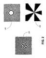
- FIG. 2is a top view of a diffractive focusing vortex lens for use in the apparatus of FIG. 1 according to an embodiment of the invention
- FIG. 3is an orthogonal view of a ring-shaped irradiance distribution pattern that results from modifying a laser beam with the diffractive focusing vortex lens of FIG. 2 according to an embodiment of the invention
- FIG. 4is a graph of the percent of flux with respect to the displacement of the aperture that passes though the aperture when using the diffractive focusing vortex lens of FIG. 2 according to a embodiment of the invention
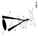
- FIG. 5is a diagram of a laser-beam modifying apparatus that uses a beam splitting device according to an embodiment of the invention
- FIG. 6Ais a top view of a two-dimensional diffractive grating for use in the apparatus of FIG. 1 according to an embodiment of the invention
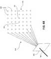
- FIG. 6Bis a plot of an array of divergent laser beams that result from a laser beam that passes through the two-dimensional diffractive grating of FIG. 6B according to an embodiment of the invention.
- FIG. 7is a block diagram of an electronic system that incorporates the apparatus of FIG. 1 according to an embodiment of the invention.
- FIG. 1is a diagram of an apparatus for modifying a laser beam for use in an optical mouse according an embodiment of the invention.
- a Vertical Cavity Surface Emitting Laser (VCSEL) 101emits an 850 nm wavelength laser beam along an optical axis 102 .
- a typical VCSEL 101will have an associated divergence angle 125 which is a measure of the widest angle at which individual rays of the laser beam emanate from the VCSEL 101 .
- the divergence angle 125is defined as the angle at which the optical intensity (power per unit area) of the laser beam falls to one-half of the peak, on-axis value.
- a typical laser beammay have a divergence angle 125 of up to about 20.
- the optical axis 102 of the VCSEL 101is aligned with a collimating lens 105 located at a distance 120 of approximately 1.5 mm from the VCSEL 101 .
- the collimating lens 105refracts the diverging laser beam 103 to produce a collimated laser beam 106 that is aligned with the optical axis 102 .
- the diameter of the collimated laser beam 106is approximately 0.62 mm.
- the collimated laser beam 106is passed through another beam modifying medium 107 , such as a lens, prism, or grating according to various embodiments of the invention as discussed below.
- another beam modifying medium 107such as a lens, prism, or grating according to various embodiments of the invention as discussed below.
- the beam-modifying medium 107is a refractive focusing lens 107 .
- the collimated laser beam 106is passed through the focusing lens 107 , which is at a distance 121 of approximately 1 mm away from the collimating lens 105 along the optical axis 102 .
- This distance 121is typically equal to thickness of an optical substrate (not shown) used to hold the lenses 105 and 107 in position.
- the focusing lens 107focuses the collimated laser beam 106 to converge at a point 108 , which is at a distance 122 of approximately 1 mm away from the focusing lens 107 along the optical axis 102 .
- the converging laser beam 109were to strike an object, such as the target 110 , the reflection would produce a speckle pattern, and a detector 111 can detect motion of the beam 109 relative to the target 110 by detecting changes in the speckle pattern. Since an optical mouse (not shown in FIG. 1 ) is typically placed on a mouse pad or other flat surface, the mouse pad or surface functions as a suitable target 110 and changes in the reflected speckle pattern, and thus movement of the mouse, may be detected by the detector 111 within the mouse.
- the convergent laser beam 109will propagate past the focal point 108 and then proceed to diverge. If one were to measure the flux of the now diverging laser beam 113 through any 7 mm aperture at a radial distance 123 of 14 mm from the focusing lens 107 (which in one embodiment is the closest point of human access as defined by the ISSPL for determining the AEL level for the laser eye-safety standard), one would find that only a portion of the diverging laser beam 113 would pass through the aperture 115 .
- the maximum fluxpasses through the aperture 115 , which has its center aligned with the axis 102 , and this maximum flux is low enough to meet the requirements for a Class 1 rating.
- the ISSPLrequires that the radial distance 123 be measured from the point where the beam 109 exits the device that generates the beam; thus, the distance 123 may be measured from other than the lens 107 in other embodiments.
- the modifying mediummay be different.
- the modifying medium 107may be a diffractive focusing vortex lens (not shown in FIG. 1 ).
- FIG. 2shows a top view of a diffractive focusing vortex lens 200 according to an embodiment of the invention.
- the diffractive focusing vortex lens 200is created by superimposing a concentric-edge microstructure lens 201 with a radial-edge microstructure lens 202 .
- the resulting effect to light, i.e., the collimated laser beam 106passed through the superimposed lenses 201 and 202 causes light to “twist” away from diffractive focusing vortex lens 200 along the optical axis 102 .
- the twisting nature of light passed through the diffractive focusing vortex lens 200results in the formation of a donut- or ring-shaped irradiance distribution pattern 300 in the plane 315 orthogonal to the optical axis 102 . That is, this phenomenon causes the pattern 300 to appear as a hollow “cone” when looking into the axis 102 toward the modifying medium 107 (which here is the lens 200 ). If designed properly, i.e., designed with the Class 1 rating in mind, the diameter of the “cone” of the ring-shaped irradiance distribution pattern 300 at the 14 mm point that corresponds to the aperture 115 position will be slightly larger than the aperture 115 diameter of 7 mm. Thus, if the aperture 115 is centered on the optical axis 102 , little or no laser light passes through it.
- a personmay not always choose to look directly into the optical axis 102 . As such, portions of the ring-shaped irradiance distribution pattern 300 may enter the eye. Depending on the angle (measured as displacement from the optical axis 102 ) one is looking, the amount of flux will also vary.
- FIG. 4is a graph that plots the percent 401 of flux passing through the aperture 115 as a function of the displacement 402 in millimeters radial from the optical axis 102 .
- a worst case scenario point 410occurs when the aperture 115 is displaced 5 mm in a direction perpendicular to the optical axis 102 .
- the maximum flux passing through the aperture at any given pointis 20%.
- a VCSEL 101may have an AEL level of up to 4 mW.
- the modifying mediumis a beam-splitting element 500 .
- the beam-splitting element 500which may include one or more prisms, is employed to reduce the amount of flux that passes through the 7 mm aperture 115 for any given viewing angle by refracting portions of the laser beam in different directions.
- the collimated laser beam 106enters the beam splitting element 500 , the collimated laser beam 106 is split into a first beam 501 and a second beam 502 .
- the two beam 501 and 502diverge at an angle 510 large enough so that at most only one beam 501 or 502 passes through the 7 mm aperture 14 mm away at any given viewing angle.
- the minimum angle 510 between any two beams 501 and 502is approximately 24.2 degrees. This effectively doubles the AEL level allowed for the VCSEL 101 beam 106 to still be within the Class 1 rating.
- Other possible beam splitting devices 500include conventional diffractive and holographic elements or multiple refractive lenses.
- the modifying medium 107may be a diffraction grating 600 as shown in FIG. 6A .
- the diffraction grating 600is a two-dimensional diffraction element that includes a double exposure of its photo-resist layer coating on a glass substrate, an x-direction exposure 601 and a y-direction exposure 602 .
- a well-known holographic exposure methodin which two collimated UV laser beams impinge on the photo-resist surface at a known angle is used to create the two-dimensional diffraction grating 600 . In this method, the interference of the two equal-power collimated ultraviolet (UV) laser beams creates a sinusoidal intensity pattern whose period depends on the angle between the beams.
- UVequal-power collimated ultraviolet
- the first exposure 601creates a latent image of a sinusoidal phase grating along the x-direction, wherein the sine wave is with respect to the depth of the cut.
- a second exposure 602creates a grating along the y-direction (also sinusoidal with respect to the depth of the cut).
- the final resultis the two-dimensional diffraction grating 600 wherein the photo-resist layer pattern is a surface relief grating with a nearly sinusoidal groove shape in both x and y directions.
- the collimated laser beam 106passes through such a two-dimensional diffraction grating 600 , the collimated laser beam 106 is diffracted into an array of divergent laser beams 615 which emanate from the two-dimensional diffraction grating 600 at various angles. If the divergent laser beams 615 were to be displayed on a distant wall for viewing, an array of light spots 616 would be seen.
- the spots 616are labeled in a simple x-y axis beginning with the center spot 620 at (0, 0).
- the spot from the first divergent laser beam 621 to the rightis (1, 0), and so on. As the distance between the display wall and the laser source becomes larger, the distance between spots also becomes larger.
- the angles between the divergent laser beams 615are determined by the period of the two-dimensional diffraction grating 600 .
- the angular separationis approximately ⁇ / ⁇ x for the x-direction, where ⁇ x is the period of the x-grating 601 and ⁇ is the laser wavelength.
- ⁇ xis the period of the x-grating 601
- ⁇is the laser wavelength.
- diffraction anglefor the y-grating 602 .
- FIG. 6Bshows a diffraction pattern for equal x-grating 601 and y-grating 602 periods ( FIG. 6A ).
- the flux in the higher orders 650decreases gradually with grating order and the higher orders 650 extend to nearly 90 degrees from the normal of the two-dimensional diffraction grating 600 .
- the fractional power diffracted into the (p,q) ordercan be shown ( Introduction to Fourier Optics, J. W. Goodman, McGraw Hill, 1968) to be:
- An advantage of using a two-dimensional diffraction grating 600 as the modifying medium 107 in the system of FIG. 1is that by designing the spatial frequency, wherein the angle between diverging laser beams 615 is high enough, typically only one of the diffraction orders can pass through the 7 mm aperture 115 . Therefore, for a 7 mm aperture 115 which is 14 mm away from two-dimensional diffraction grating 600 , the angle between divergent laser beams 615 is typically greater than about 24.2 degrees. Even if the angle between the divergent laser beams 615 is less than 24.2 degrees, so that multiple divergent laser beams 615 may enter the 7 mm aperture 115 , the divergent laser beams 615 will still not cause damage to the human eye.
- the divergent laser beams 615will not focus to a single spot on the retina, but rather an array of spots 616 . Since eye damage is typically caused by localized heating of the retina, spreading the light into an array of spots 616 reduces the possibility of damage to the eye, thus increases the maximum allowable AEL level for a VCSEL 101 .
- Firmware 726 containing the basic routines that help to transfer information between elements within the computer system 720is also contained within the system memory 722 .
- the computer system 720may further include a hard disk-drive system 727 that is also connected to the system bus 723 . Additionally, optical drives (not shown), CD-ROM drives (not shown), floppy drives (not shown) may be connected to the system bus 723 through respective drive controllers (not shown) as well.
- a usermay enter commands and information into the computer system 720 through input devices such as a keyboard 740 and an optical mouse 742 . These input devices as well as others not shown are typically connected to the system bus 723 through a serial port interface 746 . Other interfaces (not shown) include Universal Serial Bus (USB) and parallel ports 740 .
- a monitor 747 or other type of display devicemay also be connected to the system bus 723 via an interface such as the graphics card 789 .
Landscapes
- Engineering & Computer Science (AREA)
- Physics & Mathematics (AREA)
- General Engineering & Computer Science (AREA)
- Electromagnetism (AREA)
- General Physics & Mathematics (AREA)
- Theoretical Computer Science (AREA)
- Optics & Photonics (AREA)
- Condensed Matter Physics & Semiconductors (AREA)
- Civil Engineering (AREA)
- Structural Engineering (AREA)
- Human Computer Interaction (AREA)
- Environmental & Geological Engineering (AREA)
- Plasma & Fusion (AREA)
- General Life Sciences & Earth Sciences (AREA)
- Life Sciences & Earth Sciences (AREA)
- Mechanical Engineering (AREA)
- Ocean & Marine Engineering (AREA)
- Mining & Mineral Resources (AREA)
- Paleontology (AREA)
- Diffracting Gratings Or Hologram Optical Elements (AREA)
- Semiconductor Lasers (AREA)
- Position Input By Displaying (AREA)
- Lenses (AREA)
Abstract
Description
where J is the Bessel function of the first kind, the order is p or q, and m is the peak-to-peak phase delay of the two-
Claims (11)
Priority Applications (9)
| Application Number | Priority Date | Filing Date | Title |
|---|---|---|---|
| US10/366,755US7418016B2 (en) | 2003-02-13 | 2003-02-13 | Method and apparatus for modifying the spread of a laser beam |
| TW092126701ATWI312600B (en) | 2003-02-13 | 2003-09-26 | Method and apparatus for modifying the spread of a laser beam |
| DE10353381ADE10353381B8 (en) | 2003-02-13 | 2003-11-14 | Granulation-based motion detector, optical mouse, computer system and method |
| DE20321831UDE20321831U1 (en) | 2003-02-13 | 2003-11-14 | Device for modifying the spread of a laser beam |
| DE10362097ADE10362097B4 (en) | 2003-02-13 | 2003-11-14 | Method and apparatus for modifying the spread of a laser beam |
| GB0402798AGB2399675B (en) | 2003-02-13 | 2004-02-09 | Laser apparatus |
| JP2004033253AJP4448708B2 (en) | 2003-02-13 | 2004-02-10 | Method and apparatus for correcting the spread of a laser beam |
| KR1020040009212AKR101086549B1 (en) | 2003-02-13 | 2004-02-12 | Devices including laser sources and optical trains, speckle-based motion detectors, optical mice, computer systems and methods of generating and modifying laser beams |
| US11/686,228US7474680B2 (en) | 2003-02-13 | 2007-03-14 | Method and apparatus for modifying the spread of a laser beam |
Applications Claiming Priority (1)
| Application Number | Priority Date | Filing Date | Title |
|---|---|---|---|
| US10/366,755US7418016B2 (en) | 2003-02-13 | 2003-02-13 | Method and apparatus for modifying the spread of a laser beam |
Related Child Applications (1)
| Application Number | Title | Priority Date | Filing Date |
|---|---|---|---|
| US11/686,228DivisionUS7474680B2 (en) | 2003-02-13 | 2007-03-14 | Method and apparatus for modifying the spread of a laser beam |
Publications (2)
| Publication Number | Publication Date |
|---|---|
| US20040160998A1 US20040160998A1 (en) | 2004-08-19 |
| US7418016B2true US7418016B2 (en) | 2008-08-26 |
Family
ID=31993818
Family Applications (2)
| Application Number | Title | Priority Date | Filing Date |
|---|---|---|---|
| US10/366,755Expired - Fee RelatedUS7418016B2 (en) | 2003-02-13 | 2003-02-13 | Method and apparatus for modifying the spread of a laser beam |
| US11/686,228Expired - Fee RelatedUS7474680B2 (en) | 2003-02-13 | 2007-03-14 | Method and apparatus for modifying the spread of a laser beam |
Family Applications After (1)
| Application Number | Title | Priority Date | Filing Date |
|---|---|---|---|
| US11/686,228Expired - Fee RelatedUS7474680B2 (en) | 2003-02-13 | 2007-03-14 | Method and apparatus for modifying the spread of a laser beam |
Country Status (6)
| Country | Link |
|---|---|
| US (2) | US7418016B2 (en) |
| JP (1) | JP4448708B2 (en) |
| KR (1) | KR101086549B1 (en) |
| DE (3) | DE20321831U1 (en) |
| GB (1) | GB2399675B (en) |
| TW (1) | TWI312600B (en) |
Cited By (13)
| Publication number | Priority date | Publication date | Assignee | Title |
|---|---|---|---|---|
| US20060284830A1 (en)* | 2005-06-21 | 2006-12-21 | Microsoft Corporation | Input device for a computer system |
| US20100182601A1 (en)* | 2009-01-22 | 2010-07-22 | Avago Technologies Ecbu Ip (Singapore) Pte. Ltd. | Offset illumination aperture for optical navigation input device |
| US20100214224A1 (en)* | 2009-02-24 | 2010-08-26 | Avago Technologies Ecbu Ip (Singapore) Pte. Ltd. | Light beam shaping element for an optical navigation input device |
| US20100220482A1 (en)* | 2010-03-26 | 2010-09-02 | Abbatiello Robert J | Low-divergence light pointer apparatus for use through and against transparent surfaces |
| CN101554877B (en)* | 2009-05-21 | 2012-05-30 | 方岫頔 | Overlimit laser monitoring and alarming system of suspension train |
| US9869459B2 (en) | 2014-07-16 | 2018-01-16 | Telebrands Corp. | Landscape light |
| US9879847B2 (en) | 2015-12-03 | 2018-01-30 | Telebrands Corp. | Decorative lighting apparatus having two laser light sources |
| USD816890S1 (en) | 2015-05-11 | 2018-05-01 | Telebrands Corp. | Light projector |
| USD820507S1 (en) | 2015-05-11 | 2018-06-12 | Telebrands Corp. | Light projector |
| USD824066S1 (en) | 2015-05-11 | 2018-07-24 | Telebrands Corp. | Light projector |
| USD828618S1 (en) | 2015-05-11 | 2018-09-11 | Telebrands Corp. | Light projector |
| US10837609B2 (en)* | 2017-06-30 | 2020-11-17 | Streamlight, Inc. | Portable light providing plural beams of laser light |
| US20230160660A1 (en)* | 2021-11-24 | 2023-05-25 | Wrap Technologies, Inc. | Systems and Methods for Generating Optical Beam Arrays |
Families Citing this family (58)
| Publication number | Priority date | Publication date | Assignee | Title |
|---|---|---|---|---|
| JP4285955B2 (en)* | 2001-09-07 | 2009-06-24 | 三洋電機株式会社 | Hologram optical element, misregistration detection device, and optical recording medium driving device |
| US7602822B2 (en)* | 2004-09-28 | 2009-10-13 | Hitachi Via Mechanics, Ltd | Fiber laser based production of laser drilled microvias for multi-layer drilling, dicing, trimming of milling applications |
| KR100682903B1 (en)* | 2004-11-19 | 2007-02-15 | 삼성전자주식회사 | Illumination system with laser spots removed and projection TV using the same |
| KR100682902B1 (en)* | 2004-11-19 | 2007-02-15 | 삼성전자주식회사 | Illumination system with laser spots removed and projection TV using the same |
| US8212775B2 (en) | 2005-02-22 | 2012-07-03 | Pixart Imaging Incorporation | Computer input apparatus having a calibration circuit for regulating current to the light source |
| US7295733B2 (en)* | 2005-06-21 | 2007-11-13 | Finisar Corporation | Power and encircled flux alignment |
| CN101213844A (en)* | 2005-06-29 | 2008-07-02 | 皇家飞利浦电子股份有限公司 | System for scanning laser beam image projection with divergent beam and corresponding method |
| US7466886B2 (en)* | 2005-07-08 | 2008-12-16 | Finisar Corporation | Coupling region for optical systems |
| TWI361286B (en)* | 2008-02-01 | 2012-04-01 | Pixart Imaging Inc | Optical pointing device |
| US8908995B2 (en) | 2009-01-12 | 2014-12-09 | Intermec Ip Corp. | Semi-automatic dimensioning with imager on a portable device |
| US8330721B2 (en)* | 2009-02-19 | 2012-12-11 | Avago Technologies Ecbu Ip (Singapore) Pte. Ltd. | Optical navigation device with phase grating for beam steering |
| JP2012102903A (en)* | 2010-11-08 | 2012-05-31 | Nippon Koki Co Ltd | Laser emitting device |
| CN102148067B (en)* | 2011-01-27 | 2013-10-09 | 西北工业大学 | A device for generating a rotating compound vortex beam |
| US8837883B2 (en)* | 2011-09-23 | 2014-09-16 | Alcon Research, Ltd. | Shaping laser beam launches into optical fibers to yield specific output effects |
| US9779546B2 (en) | 2012-05-04 | 2017-10-03 | Intermec Ip Corp. | Volume dimensioning systems and methods |
| US10007858B2 (en) | 2012-05-15 | 2018-06-26 | Honeywell International Inc. | Terminals and methods for dimensioning objects |
| US10321127B2 (en) | 2012-08-20 | 2019-06-11 | Intermec Ip Corp. | Volume dimensioning system calibration systems and methods |
| US9939259B2 (en) | 2012-10-04 | 2018-04-10 | Hand Held Products, Inc. | Measuring object dimensions using mobile computer |
| US20140104413A1 (en) | 2012-10-16 | 2014-04-17 | Hand Held Products, Inc. | Integrated dimensioning and weighing system |
| US9080856B2 (en) | 2013-03-13 | 2015-07-14 | Intermec Ip Corp. | Systems and methods for enhancing dimensioning, for example volume dimensioning |
| US10228452B2 (en) | 2013-06-07 | 2019-03-12 | Hand Held Products, Inc. | Method of error correction for 3D imaging device |
| WO2014204468A1 (en) | 2013-06-20 | 2014-12-24 | Hewlett-Packard Development Company, Lp | Mode-controlled laser system |
| US20150070489A1 (en)* | 2013-09-11 | 2015-03-12 | Microsoft Corporation | Optical modules for use with depth cameras |
| KR102381930B1 (en)* | 2014-03-13 | 2022-04-04 | 내셔널 유니버시티 오브 싱가포르 | An optical interference device |
| US9823059B2 (en) | 2014-08-06 | 2017-11-21 | Hand Held Products, Inc. | Dimensioning system with guided alignment |
| US10810715B2 (en) | 2014-10-10 | 2020-10-20 | Hand Held Products, Inc | System and method for picking validation |
| US9779276B2 (en) | 2014-10-10 | 2017-10-03 | Hand Held Products, Inc. | Depth sensor based auto-focus system for an indicia scanner |
| US10775165B2 (en) | 2014-10-10 | 2020-09-15 | Hand Held Products, Inc. | Methods for improving the accuracy of dimensioning-system measurements |
| US9752864B2 (en) | 2014-10-21 | 2017-09-05 | Hand Held Products, Inc. | Handheld dimensioning system with feedback |
| US9897434B2 (en) | 2014-10-21 | 2018-02-20 | Hand Held Products, Inc. | Handheld dimensioning system with measurement-conformance feedback |
| US9762793B2 (en) | 2014-10-21 | 2017-09-12 | Hand Held Products, Inc. | System and method for dimensioning |
| US9557166B2 (en) | 2014-10-21 | 2017-01-31 | Hand Held Products, Inc. | Dimensioning system with multipath interference mitigation |
| US10060729B2 (en) | 2014-10-21 | 2018-08-28 | Hand Held Products, Inc. | Handheld dimensioner with data-quality indication |
| US9786101B2 (en) | 2015-05-19 | 2017-10-10 | Hand Held Products, Inc. | Evaluating image values |
| US10066982B2 (en) | 2015-06-16 | 2018-09-04 | Hand Held Products, Inc. | Calibrating a volume dimensioner |
| US9857167B2 (en) | 2015-06-23 | 2018-01-02 | Hand Held Products, Inc. | Dual-projector three-dimensional scanner |
| US20160377414A1 (en)* | 2015-06-23 | 2016-12-29 | Hand Held Products, Inc. | Optical pattern projector |
| US9835486B2 (en) | 2015-07-07 | 2017-12-05 | Hand Held Products, Inc. | Mobile dimensioner apparatus for use in commerce |
| EP3118576B1 (en) | 2015-07-15 | 2018-09-12 | Hand Held Products, Inc. | Mobile dimensioning device with dynamic accuracy compatible with nist standard |
| US10094650B2 (en) | 2015-07-16 | 2018-10-09 | Hand Held Products, Inc. | Dimensioning and imaging items |
| US20170017301A1 (en) | 2015-07-16 | 2017-01-19 | Hand Held Products, Inc. | Adjusting dimensioning results using augmented reality |
| US10249030B2 (en) | 2015-10-30 | 2019-04-02 | Hand Held Products, Inc. | Image transformation for indicia reading |
| US10225544B2 (en) | 2015-11-19 | 2019-03-05 | Hand Held Products, Inc. | High resolution dot pattern |
| US10025314B2 (en) | 2016-01-27 | 2018-07-17 | Hand Held Products, Inc. | Vehicle positioning and object avoidance |
| US10339352B2 (en) | 2016-06-03 | 2019-07-02 | Hand Held Products, Inc. | Wearable metrological apparatus |
| US9940721B2 (en) | 2016-06-10 | 2018-04-10 | Hand Held Products, Inc. | Scene change detection in a dimensioner |
| US10163216B2 (en) | 2016-06-15 | 2018-12-25 | Hand Held Products, Inc. | Automatic mode switching in a volume dimensioner |
| US10909708B2 (en) | 2016-12-09 | 2021-02-02 | Hand Held Products, Inc. | Calibrating a dimensioner using ratios of measurable parameters of optic ally-perceptible geometric elements |
| US11047672B2 (en) | 2017-03-28 | 2021-06-29 | Hand Held Products, Inc. | System for optically dimensioning |
| US10733748B2 (en) | 2017-07-24 | 2020-08-04 | Hand Held Products, Inc. | Dual-pattern optical 3D dimensioning |
| CN107621701B (en)* | 2017-09-07 | 2023-08-25 | 苏州大学 | Method and system for generating double-index Bessel Gaussian beam |
| EP3711123A4 (en)* | 2017-11-16 | 2021-08-25 | Princeton Optronics, Inc. | Structured light illuminators including a chief ray corrector optical element |
| US10705001B2 (en)* | 2018-04-23 | 2020-07-07 | Artium Technologies, Inc. | Particle field imaging and characterization using VCSEL lasers for convergent multi-beam illumination |
| US10584962B2 (en) | 2018-05-01 | 2020-03-10 | Hand Held Products, Inc | System and method for validating physical-item security |
| US11318048B2 (en) | 2018-08-31 | 2022-05-03 | Iridex Corporation | Methods and systems for large spot retinal laser treatment |
| US11175010B2 (en) | 2018-09-20 | 2021-11-16 | Samsung Electronics Co., Ltd. | Illumination device and electronic apparatus including the same |
| US11639846B2 (en) | 2019-09-27 | 2023-05-02 | Honeywell International Inc. | Dual-pattern optical 3D dimensioning |
| CN113223744B (en)* | 2021-04-21 | 2022-10-25 | 太原理工大学 | An optical micromanipulation device and method for ultrafast manipulation of vector vortex optical fields |
Citations (31)
| Publication number | Priority date | Publication date | Assignee | Title |
|---|---|---|---|---|
| US4402574A (en)* | 1981-04-20 | 1983-09-06 | Weyerhaeuser Company | Method and apparatus for refracting a laser beam |
| US4521772A (en) | 1981-08-28 | 1985-06-04 | Xerox Corporation | Cursor control device |
| US4645302A (en) | 1982-12-21 | 1987-02-24 | Crosfield Electronics Limited | Light beam-splitter |
| US4794384A (en) | 1984-09-27 | 1988-12-27 | Xerox Corporation | Optical translator device |
| US5016149A (en) | 1988-11-24 | 1991-05-14 | Hitachi, Ltd. | Illuminating method and illuminating apparatus for carrying out the same, and projection exposure method and projection exposure apparatus for carrying out the same |
| DE4335244A1 (en) | 1993-10-15 | 1995-06-22 | Daimler Benz Ag | Device for improving driver visibility in automobiles |
| US5719702A (en) | 1993-08-03 | 1998-02-17 | The United States Of America As Represented By The United States Department Of Energy | Polarization-balanced beamsplitter |
| US5799119A (en) | 1996-07-03 | 1998-08-25 | Northern Telecom Limited | Coupling of strongly and weakly guiding waveguides for compact integrated mach zehnder modulators |
| US5835514A (en)* | 1996-01-25 | 1998-11-10 | Hewlett-Packard Company | Laser-based controlled-intensity light source using reflection from a convex surface and method of making same |
| US6007218A (en)* | 1995-08-23 | 1999-12-28 | Science & Engineering Associates, Inc. | Self-contained laser illuminator module |
| WO2000013051A1 (en) | 1998-08-31 | 2000-03-09 | Digital Optics Corporation | Diffractive vertical cavity surface emitting laser power monitor and system |
| US6064786A (en) | 1996-03-08 | 2000-05-16 | Hewlett-Packard Company | Multimode communications systems and method using same |
| US6154319A (en) | 1997-07-03 | 2000-11-28 | Levelite Technology Inc. | Multiple laser beam generation |
| US6222174B1 (en) | 1999-03-05 | 2001-04-24 | Hewlett-Packard Company | Method of correlating immediately acquired and previously stored feature information for motion sensing |
| US6236520B1 (en) | 1997-03-07 | 2001-05-22 | Daimlerchrysler Ag | Lighting device for picture recording |
| US6256016B1 (en) | 1997-06-05 | 2001-07-03 | Logitech, Inc. | Optical detection system, device, and method utilizing optical matching |
| US6264377B1 (en) | 1998-03-06 | 2001-07-24 | Matsushita Electric Industrial Co., Ltd. | Bidirectional optical semiconductor apparatus |
| EP1170707A2 (en) | 2000-07-03 | 2002-01-09 | BUNDESDRUCKEREI GmbH | Portable sensor for validating marks on documents |
| US6496621B1 (en) | 1998-09-22 | 2002-12-17 | Digital Optics Corp. | Fiber coupler system and associated methods for reducing back reflections |
| EP1279988A2 (en) | 2001-07-23 | 2003-01-29 | Giesecke & Devrient GmbH | Laser illumination device for illuminating a line or a strip-like area |
| US6530697B1 (en)* | 1998-09-22 | 2003-03-11 | Digital Optics Corp. | Multi-mode fiber coupler, system and associated methods |
| US20030123508A1 (en) | 2001-12-28 | 2003-07-03 | Werner Thomas R. | Integral vertical cavity surface emitting laser and power monitor |
| US20030141465A1 (en)* | 2001-12-17 | 2003-07-31 | Schuda Felix J. | Semiconductor wafer carrier mapping sensor |
| US6617577B2 (en)* | 2001-04-16 | 2003-09-09 | The Rockefeller University | Method and system for mass spectroscopy |
| US20040008414A1 (en) | 2000-12-15 | 2004-01-15 | Coleman Christopher L. | Diffractive optical element for providing favorable multi-mode fiber launch and reflection management |
| WO2004006793A1 (en) | 2002-07-11 | 2004-01-22 | Asah Medico A/S | An apparatus for tissue treatment |
| US6741335B2 (en)* | 1998-03-09 | 2004-05-25 | Otm Technologies Ltd. | Optical translation measurement |
| US20040120717A1 (en)* | 2002-12-18 | 2004-06-24 | Lightpointe Communications, Inc. | Extended source free-space optical communication system |
| US20040169929A1 (en) | 2001-09-13 | 2004-09-02 | Asahi Glass Company Limited | Diffraction element |
| US6801354B1 (en)* | 2002-08-20 | 2004-10-05 | Silicon Light Machines, Inc. | 2-D diffraction grating for substantially eliminating polarization dependent losses |
| US20040201894A1 (en) | 2000-06-16 | 2004-10-14 | Brown David Renick | Off-axis diffractive beam shapers and splitters for reducing sensitivity to manufacturing tolerances |
Family Cites Families (2)
| Publication number | Priority date | Publication date | Assignee | Title |
|---|---|---|---|---|
| CA2097360A1 (en)* | 1992-06-03 | 1993-12-04 | Paul Dvorkis | Optical readers |
| US5771254A (en)* | 1996-01-25 | 1998-06-23 | Hewlett-Packard Company | Integrated controlled intensity laser-based light source |
- 2003
- 2003-02-13USUS10/366,755patent/US7418016B2/ennot_activeExpired - Fee Related
- 2003-09-26TWTW092126701Apatent/TWI312600B/ennot_activeIP Right Cessation
- 2003-11-14DEDE20321831Upatent/DE20321831U1/ennot_activeExpired - Lifetime
- 2003-11-14DEDE10353381Apatent/DE10353381B8/ennot_activeExpired - Fee Related
- 2003-11-14DEDE10362097Apatent/DE10362097B4/ennot_activeExpired - Fee Related
- 2004
- 2004-02-09GBGB0402798Apatent/GB2399675B/ennot_activeExpired - Fee Related
- 2004-02-10JPJP2004033253Apatent/JP4448708B2/ennot_activeExpired - Fee Related
- 2004-02-12KRKR1020040009212Apatent/KR101086549B1/ennot_activeExpired - Fee Related
- 2007
- 2007-03-14USUS11/686,228patent/US7474680B2/ennot_activeExpired - Fee Related
Patent Citations (37)
| Publication number | Priority date | Publication date | Assignee | Title |
|---|---|---|---|---|
| US4402574A (en)* | 1981-04-20 | 1983-09-06 | Weyerhaeuser Company | Method and apparatus for refracting a laser beam |
| US4521772A (en) | 1981-08-28 | 1985-06-04 | Xerox Corporation | Cursor control device |
| US4645302A (en) | 1982-12-21 | 1987-02-24 | Crosfield Electronics Limited | Light beam-splitter |
| US4794384A (en) | 1984-09-27 | 1988-12-27 | Xerox Corporation | Optical translator device |
| US5016149A (en) | 1988-11-24 | 1991-05-14 | Hitachi, Ltd. | Illuminating method and illuminating apparatus for carrying out the same, and projection exposure method and projection exposure apparatus for carrying out the same |
| US5719702A (en) | 1993-08-03 | 1998-02-17 | The United States Of America As Represented By The United States Department Of Energy | Polarization-balanced beamsplitter |
| DE4335244A1 (en) | 1993-10-15 | 1995-06-22 | Daimler Benz Ag | Device for improving driver visibility in automobiles |
| US6007218A (en)* | 1995-08-23 | 1999-12-28 | Science & Engineering Associates, Inc. | Self-contained laser illuminator module |
| US5835514A (en)* | 1996-01-25 | 1998-11-10 | Hewlett-Packard Company | Laser-based controlled-intensity light source using reflection from a convex surface and method of making same |
| US6064786A (en) | 1996-03-08 | 2000-05-16 | Hewlett-Packard Company | Multimode communications systems and method using same |
| US5799119A (en) | 1996-07-03 | 1998-08-25 | Northern Telecom Limited | Coupling of strongly and weakly guiding waveguides for compact integrated mach zehnder modulators |
| EP0964782B1 (en) | 1997-03-07 | 2002-08-07 | Astrium GmbH | Lighting device for picture recording |
| US6236520B1 (en) | 1997-03-07 | 2001-05-22 | Daimlerchrysler Ag | Lighting device for picture recording |
| US6256016B1 (en) | 1997-06-05 | 2001-07-03 | Logitech, Inc. | Optical detection system, device, and method utilizing optical matching |
| US6154319A (en) | 1997-07-03 | 2000-11-28 | Levelite Technology Inc. | Multiple laser beam generation |
| US6264377B1 (en) | 1998-03-06 | 2001-07-24 | Matsushita Electric Industrial Co., Ltd. | Bidirectional optical semiconductor apparatus |
| US6741335B2 (en)* | 1998-03-09 | 2004-05-25 | Otm Technologies Ltd. | Optical translation measurement |
| WO2000013051A1 (en) | 1998-08-31 | 2000-03-09 | Digital Optics Corporation | Diffractive vertical cavity surface emitting laser power monitor and system |
| US20030142903A1 (en)* | 1998-09-22 | 2003-07-31 | Johnson Eric G. | Multi-mode fiber coupler, system and associated methods |
| US6496621B1 (en) | 1998-09-22 | 2002-12-17 | Digital Optics Corp. | Fiber coupler system and associated methods for reducing back reflections |
| US6530697B1 (en)* | 1998-09-22 | 2003-03-11 | Digital Optics Corp. | Multi-mode fiber coupler, system and associated methods |
| US6222174B1 (en) | 1999-03-05 | 2001-04-24 | Hewlett-Packard Company | Method of correlating immediately acquired and previously stored feature information for motion sensing |
| US20040201894A1 (en) | 2000-06-16 | 2004-10-14 | Brown David Renick | Off-axis diffractive beam shapers and splitters for reducing sensitivity to manufacturing tolerances |
| US6784441B2 (en) | 2000-07-03 | 2004-08-31 | Bundesdruckerei Gmbh | Handsensor for authenticity identification of signets on documents |
| EP1170707A2 (en) | 2000-07-03 | 2002-01-09 | BUNDESDRUCKEREI GmbH | Portable sensor for validating marks on documents |
| US20040008414A1 (en) | 2000-12-15 | 2004-01-15 | Coleman Christopher L. | Diffractive optical element for providing favorable multi-mode fiber launch and reflection management |
| US6856460B2 (en)* | 2000-12-15 | 2005-02-15 | Agilent Technologies, Inc. | Diffractive optical element for providing favorable multi-mode fiber launch and reflection management |
| US20040201893A1 (en)* | 2000-12-15 | 2004-10-14 | Coleman Christopher L. | Diffractive optical element for providing favorable multi-mode fiber launch and reflection management |
| US6617577B2 (en)* | 2001-04-16 | 2003-09-09 | The Rockefeller University | Method and system for mass spectroscopy |
| EP1279988A2 (en) | 2001-07-23 | 2003-01-29 | Giesecke & Devrient GmbH | Laser illumination device for illuminating a line or a strip-like area |
| US6845119B2 (en) | 2001-07-23 | 2005-01-18 | Giesecke & Devrient Gmbh | Laser illuminating apparatus for illuminating a strip-shaped or linear area |
| US20040169929A1 (en) | 2001-09-13 | 2004-09-02 | Asahi Glass Company Limited | Diffraction element |
| US20030141465A1 (en)* | 2001-12-17 | 2003-07-31 | Schuda Felix J. | Semiconductor wafer carrier mapping sensor |
| US20030123508A1 (en) | 2001-12-28 | 2003-07-03 | Werner Thomas R. | Integral vertical cavity surface emitting laser and power monitor |
| WO2004006793A1 (en) | 2002-07-11 | 2004-01-22 | Asah Medico A/S | An apparatus for tissue treatment |
| US6801354B1 (en)* | 2002-08-20 | 2004-10-05 | Silicon Light Machines, Inc. | 2-D diffraction grating for substantially eliminating polarization dependent losses |
| US20040120717A1 (en)* | 2002-12-18 | 2004-06-24 | Lightpointe Communications, Inc. | Extended source free-space optical communication system |
Non-Patent Citations (3)
| Title |
|---|
| English translation of German Office Action dated Feb. 22, 2005; German Patent Application No. 103 53 381.8-51. |
| International Search Report 2003 |
| International Search Reposrt. |
Cited By (25)
| Publication number | Priority date | Publication date | Assignee | Title |
|---|---|---|---|---|
| US20060284830A1 (en)* | 2005-06-21 | 2006-12-21 | Microsoft Corporation | Input device for a computer system |
| US7719517B2 (en)* | 2005-06-21 | 2010-05-18 | Microsoft Corporation | Input device for a computer system |
| US20100182601A1 (en)* | 2009-01-22 | 2010-07-22 | Avago Technologies Ecbu Ip (Singapore) Pte. Ltd. | Offset illumination aperture for optical navigation input device |
| US8164569B2 (en) | 2009-01-22 | 2012-04-24 | Avago Technologies Ecbu Ip (Singapore) Pte. Ltd. | Offset illumination aperture for optical navigation input device |
| US20100214224A1 (en)* | 2009-02-24 | 2010-08-26 | Avago Technologies Ecbu Ip (Singapore) Pte. Ltd. | Light beam shaping element for an optical navigation input device |
| US8259068B2 (en) | 2009-02-24 | 2012-09-04 | Avago Technologies Ecbu Ip (Singapore) Pte. Ltd. | Light beam shaping element for an optical navigation input device |
| CN101554877B (en)* | 2009-05-21 | 2012-05-30 | 方岫頔 | Overlimit laser monitoring and alarming system of suspension train |
| US20100220482A1 (en)* | 2010-03-26 | 2010-09-02 | Abbatiello Robert J | Low-divergence light pointer apparatus for use through and against transparent surfaces |
| US8376586B2 (en) | 2010-03-26 | 2013-02-19 | Robert J. Abbatiello | Low-divergence light pointer apparatus for use through and against transparent surfaces |
| US10197234B2 (en) | 2014-07-16 | 2019-02-05 | Telebrands Corp. | Landscape light |
| US9874327B2 (en) | 2014-07-16 | 2018-01-23 | Telebrands Corp. | Landscape light |
| US10228113B2 (en) | 2014-07-16 | 2019-03-12 | Telebrands Corp. | Landscape light |
| US9869459B2 (en) | 2014-07-16 | 2018-01-16 | Telebrands Corp. | Landscape light |
| USD820507S1 (en) | 2015-05-11 | 2018-06-12 | Telebrands Corp. | Light projector |
| USD821023S1 (en) | 2015-05-11 | 2018-06-19 | Telebrands Corp. | Light projector |
| USD824066S1 (en) | 2015-05-11 | 2018-07-24 | Telebrands Corp. | Light projector |
| USD828618S1 (en) | 2015-05-11 | 2018-09-11 | Telebrands Corp. | Light projector |
| USD828619S1 (en) | 2015-05-11 | 2018-09-11 | Telebrands Corp. | Light projector |
| USD816890S1 (en) | 2015-05-11 | 2018-05-01 | Telebrands Corp. | Light projector |
| US9879847B2 (en) | 2015-12-03 | 2018-01-30 | Telebrands Corp. | Decorative lighting apparatus having two laser light sources |
| US10837609B2 (en)* | 2017-06-30 | 2020-11-17 | Streamlight, Inc. | Portable light providing plural beams of laser light |
| US20230160660A1 (en)* | 2021-11-24 | 2023-05-25 | Wrap Technologies, Inc. | Systems and Methods for Generating Optical Beam Arrays |
| US11852439B2 (en)* | 2021-11-24 | 2023-12-26 | Wrap Technologies, Inc. | Systems and methods for generating optical beam arrays |
| US20240288247A1 (en)* | 2021-11-24 | 2024-08-29 | Wrap Technologies, Inc. | Systems and Methods for Generating Optical Beam Arrays |
| US12228371B2 (en)* | 2021-11-24 | 2025-02-18 | Wrap Technologies, Inc. | Systems and methods for generating optical beam arrays |
Also Published As
| Publication number | Publication date |
|---|---|
| US20040160998A1 (en) | 2004-08-19 |
| US7474680B2 (en) | 2009-01-06 |
| JP4448708B2 (en) | 2010-04-14 |
| DE20321831U1 (en) | 2011-01-05 |
| DE10362097B4 (en) | 2011-06-22 |
| DE10353381B4 (en) | 2010-11-25 |
| DE10353381B8 (en) | 2011-04-07 |
| DE10353381A1 (en) | 2004-09-02 |
| GB0402798D0 (en) | 2004-03-10 |
| JP2004246360A (en) | 2004-09-02 |
| KR101086549B1 (en) | 2011-11-23 |
| GB2399675A (en) | 2004-09-22 |
| TW200415830A (en) | 2004-08-16 |
| GB2399675B (en) | 2007-08-29 |
| US20070153293A1 (en) | 2007-07-05 |
| TWI312600B (en) | 2009-07-21 |
| KR20040073373A (en) | 2004-08-19 |
Similar Documents
| Publication | Publication Date | Title |
|---|---|---|
| US7418016B2 (en) | Method and apparatus for modifying the spread of a laser beam | |
| US7633633B2 (en) | Position determination that is responsive to a retro-reflective object | |
| US9069124B2 (en) | Device, a system and a method of encoding a position of an object | |
| EP1716476B1 (en) | Optical input device based on doppler shift and laser self-mixing | |
| JP2009109513A (en) | Optical displacement sensor | |
| EP3596446B1 (en) | Laser sensor module for particle detection with offset beam | |
| WO2006021911A1 (en) | Position and orientation detection for an optical identifier | |
| JP2009525493A (en) | Laser light beam focusing apparatus and method | |
| US8821035B2 (en) | Optical element and system using the same | |
| US10310281B1 (en) | Optical projector with off-axis diffractive element | |
| CN211374004U (en) | Waveguide sheet detection device | |
| EP1429235B1 (en) | An input device for screen navigation, such as cursor control on a computer screen | |
| EP0458274B1 (en) | Apparatus and method for detecting an information of the displacement of an object. | |
| US6276800B1 (en) | System for modeling a wavefront using sheared phase shifts | |
| US11269191B2 (en) | Data acquisition apparatus | |
| US20240009761A1 (en) | Device and Method for Determining a Focal Point | |
| US20070052975A1 (en) | Arrangement for the optical distance determination of a reflecting surface | |
| JPH09305692A (en) | Laser beam generating optical element and bar code reader using the laser beam generating optical element | |
| WO2025083444A1 (en) | Eye tracking system, eye glasses and method for operating an eye tracking system | |
| Hasman et al. | Multifunctional holographic elements for surface measurements | |
| HK1073500B (en) | Optical displacement sensor | |
| Seppala | Lens Design And The Ghost Focus Problem In Fusion Lasers | |
| Slangen et al. | Speckles, From Grains fo Flowers |
Legal Events
| Date | Code | Title | Description |
|---|---|---|---|
| AS | Assignment | Owner name:AGILENT TECHNOLOGIES, INC., COLORADO Free format text:ASSIGNMENT OF ASSIGNORS INTEREST;ASSIGNORS:GRUHLKE, RUSSELL W.;TRUTNA, WILLIAM RICHARD, JR.;REEL/FRAME:013708/0330;SIGNING DATES FROM 20030228 TO 20030303 | |
| AS | Assignment | Owner name:AVAGO TECHNOLOGIES GENERAL IP PTE. LTD.,SINGAPORE Free format text:ASSIGNMENT OF ASSIGNORS INTEREST;ASSIGNOR:AGILENT TECHNOLOGIES, INC.;REEL/FRAME:017206/0666 Effective date:20051201 Owner name:AVAGO TECHNOLOGIES GENERAL IP PTE. LTD., SINGAPORE Free format text:ASSIGNMENT OF ASSIGNORS INTEREST;ASSIGNOR:AGILENT TECHNOLOGIES, INC.;REEL/FRAME:017206/0666 Effective date:20051201 | |
| AS | Assignment | Owner name:CITICORP NORTH AMERICA, INC.,DELAWARE Free format text:SECURITY AGREEMENT;ASSIGNOR:AVAGO TECHNOLOGIES GENERAL IP (SINGAPORE) PTE. LTD.;REEL/FRAME:017207/0882 Effective date:20051201 Owner name:CITICORP NORTH AMERICA, INC., DELAWARE Free format text:SECURITY AGREEMENT;ASSIGNOR:AVAGO TECHNOLOGIES GENERAL IP (SINGAPORE) PTE. LTD.;REEL/FRAME:017207/0882 Effective date:20051201 | |
| AS | Assignment | Owner name:AVAGO TECHNOLOGIES ECBU IP (SINGAPORE) PTE. LTD., SINGAPORE Free format text:ASSIGNMENT OF ASSIGNORS INTEREST;ASSIGNOR:AVAGO TECHNOLOGIES GENERAL IP (SINGAPORE) PTE. LTD.;REEL/FRAME:017675/0518 Effective date:20060127 Owner name:AVAGO TECHNOLOGIES ECBU IP (SINGAPORE) PTE. LTD.,S Free format text:ASSIGNMENT OF ASSIGNORS INTEREST;ASSIGNOR:AVAGO TECHNOLOGIES GENERAL IP (SINGAPORE) PTE. LTD.;REEL/FRAME:017675/0518 Effective date:20060127 Owner name:AVAGO TECHNOLOGIES ECBU IP (SINGAPORE) PTE. LTD., Free format text:ASSIGNMENT OF ASSIGNORS INTEREST;ASSIGNOR:AVAGO TECHNOLOGIES GENERAL IP (SINGAPORE) PTE. LTD.;REEL/FRAME:017675/0518 Effective date:20060127 | |
| FPAY | Fee payment | Year of fee payment:4 | |
| AS | Assignment | Owner name:AVAGO TECHNOLOGIES ECBU IP (SINGAPORE) PTE. LTD., Free format text:RELEASE BY SECURED PARTY;ASSIGNOR:CITICORP NORTH AMERICA, INC.;REEL/FRAME:028954/0001 Effective date:20110331 | |
| AS | Assignment | Owner name:AVAGO TECHNOLOGIES GENERAL IP (SINGAPORE) PTE. LTD Free format text:MERGER;ASSIGNOR:AVAGO TECHNOLOGIES ECBU IP (SINGAPORE) PTE. LTD.;REEL/FRAME:030369/0528 Effective date:20121030 | |
| REMI | Maintenance fee reminder mailed | ||
| AS | Assignment | Owner name:AVAGO TECHNOLOGIES GENERAL IP (SINGAPORE) PTE. LTD Free format text:CORRECTIVE ASSIGNMENT TO CORRECT THE ASSIGNEE NAME PREVIOUSLY RECORDED AT REEL: 017206 FRAME: 0666. ASSIGNOR(S) HEREBY CONFIRMS THE ASSIGNMENT;ASSIGNOR:AGILENT TECHNOLOGIES, INC.;REEL/FRAME:038632/0662 Effective date:20051201 | |
| LAPS | Lapse for failure to pay maintenance fees | ||
| STCH | Information on status: patent discontinuation | Free format text:PATENT EXPIRED DUE TO NONPAYMENT OF MAINTENANCE FEES UNDER 37 CFR 1.362 | |
| FP | Lapsed due to failure to pay maintenance fee | Effective date:20160826 |