US7417266B1 - MOSFET having a JFET embedded as a body diode - Google Patents
MOSFET having a JFET embedded as a body diodeDownload PDFInfo
- Publication number
- US7417266B1 US7417266B1US11/149,718US14971805AUS7417266B1US 7417266 B1US7417266 B1US 7417266B1US 14971805 AUS14971805 AUS 14971805AUS 7417266 B1US7417266 B1US 7417266B1
- Authority
- US
- United States
- Prior art keywords
- region
- doped
- regions
- source
- lightly
- Prior art date
- Legal status (The legal status is an assumption and is not a legal conclusion. Google has not performed a legal analysis and makes no representation as to the accuracy of the status listed.)
- Expired - Fee Related, expires
Links
- 239000004065semiconductorSubstances0.000claimsabstractdescription122
- 230000005669field effectEffects0.000claimsabstractdescription49
- 210000000746body regionAnatomy0.000claimsdescription151
- 239000012212insulatorSubstances0.000claimsdescription50
- 229910052751metalInorganic materials0.000claimsdescription36
- 239000002184metalSubstances0.000claimsdescription36
- 239000000758substrateSubstances0.000claimsdescription31
- 238000000034methodMethods0.000description58
- 229910052698phosphorusInorganic materials0.000description50
- XUIMIQQOPSSXEZ-UHFFFAOYSA-NSiliconChemical compound[Si]XUIMIQQOPSSXEZ-UHFFFAOYSA-N0.000description46
- 229910052710siliconInorganic materials0.000description46
- 239000010703siliconSubstances0.000description46
- OAICVXFJPJFONN-UHFFFAOYSA-NPhosphorusChemical compound[P]OAICVXFJPJFONN-UHFFFAOYSA-N0.000description38
- 239000011574phosphorusSubstances0.000description38
- ZOXJGFHDIHLPTG-UHFFFAOYSA-NBoronChemical compound[B]ZOXJGFHDIHLPTG-UHFFFAOYSA-N0.000description32
- 229910052796boronInorganic materials0.000description32
- 229910052785arsenicInorganic materials0.000description30
- RQNWIZPPADIBDY-UHFFFAOYSA-Narsenic atomChemical compound[As]RQNWIZPPADIBDY-UHFFFAOYSA-N0.000description30
- VYPSYNLAJGMNEJ-UHFFFAOYSA-NSilicium dioxideChemical compoundO=[Si]=OVYPSYNLAJGMNEJ-UHFFFAOYSA-N0.000description24
- 239000002019doping agentSubstances0.000description24
- 229910021420polycrystalline siliconInorganic materials0.000description22
- 229920005591polysiliconPolymers0.000description22
- 235000012239silicon dioxideNutrition0.000description12
- 239000000377silicon dioxideSubstances0.000description12
- 238000005530etchingMethods0.000description11
- 238000004380ashingMethods0.000description9
- 238000000151depositionMethods0.000description9
- 238000001459lithographyMethods0.000description9
- JBRZTFJDHDCESZ-UHFFFAOYSA-NAsGaChemical compound[As]#[Ga]JBRZTFJDHDCESZ-UHFFFAOYSA-N0.000description8
- 229910001218Gallium arsenideInorganic materials0.000description8
- GPXJNWSHGFTCBW-UHFFFAOYSA-NIndium phosphideChemical compound[In]#PGPXJNWSHGFTCBW-UHFFFAOYSA-N0.000description8
- 239000012535impuritySubstances0.000description7
- 238000004519manufacturing processMethods0.000description7
- 230000015572biosynthetic processEffects0.000description6
- 230000008021depositionEffects0.000description6
- 238000005137deposition processMethods0.000description5
- 229910021332silicideInorganic materials0.000description5
- BLRPTPMANUNPDV-UHFFFAOYSA-NSilaneChemical group[SiH4]BLRPTPMANUNPDV-UHFFFAOYSA-N0.000description4
- 230000015556catabolic processEffects0.000description4
- 238000004140cleaningMethods0.000description4
- 238000010586diagramMethods0.000description4
- 230000000694effectsEffects0.000description4
- 239000007943implantSubstances0.000description4
- 230000003647oxidationEffects0.000description4
- 238000007254oxidation reactionMethods0.000description4
- 238000011084recoveryMethods0.000description4
- FVBUAEGBCNSCDD-UHFFFAOYSA-Nsilicide(4-)Chemical compound[Si-4]FVBUAEGBCNSCDD-UHFFFAOYSA-N0.000description4
- 238000012986modificationMethods0.000description3
- 230000004048modificationEffects0.000description3
- 238000000137annealingMethods0.000description2
- 230000004888barrier functionEffects0.000description2
- 238000000354decomposition reactionMethods0.000description2
- 238000002347injectionMethods0.000description2
- 239000007924injectionSubstances0.000description2
- 230000001590oxidative effectEffects0.000description2
- 238000002161passivationMethods0.000description2
- BASFCYQUMIYNBI-UHFFFAOYSA-NplatinumChemical compound[Pt]BASFCYQUMIYNBI-UHFFFAOYSA-N0.000description2
- 229910000077silaneInorganic materials0.000description2
- 238000004544sputter depositionMethods0.000description2
- RTAQQCXQSZGOHL-UHFFFAOYSA-NTitaniumChemical compound[Ti]RTAQQCXQSZGOHL-UHFFFAOYSA-N0.000description1
- 229910017052cobaltInorganic materials0.000description1
- 239000010941cobaltSubstances0.000description1
- GUTLYIVDDKVIGB-UHFFFAOYSA-Ncobalt atomChemical compound[Co]GUTLYIVDDKVIGB-UHFFFAOYSA-N0.000description1
- 229910052697platinumInorganic materials0.000description1
- 238000005498polishingMethods0.000description1
- 229910052719titaniumInorganic materials0.000description1
- 239000010936titaniumSubstances0.000description1
Images


Classifications
- H—ELECTRICITY
- H10—SEMICONDUCTOR DEVICES; ELECTRIC SOLID-STATE DEVICES NOT OTHERWISE PROVIDED FOR
- H10D—INORGANIC ELECTRIC SEMICONDUCTOR DEVICES
- H10D30/00—Field-effect transistors [FET]
- H10D30/01—Manufacture or treatment
- H10D30/021—Manufacture or treatment of FETs having insulated gates [IGFET]
- H10D30/028—Manufacture or treatment of FETs having insulated gates [IGFET] of double-diffused metal oxide semiconductor [DMOS] FETs
- H10D30/0291—Manufacture or treatment of FETs having insulated gates [IGFET] of double-diffused metal oxide semiconductor [DMOS] FETs of vertical DMOS [VDMOS] FETs
- H10D30/0297—Manufacture or treatment of FETs having insulated gates [IGFET] of double-diffused metal oxide semiconductor [DMOS] FETs of vertical DMOS [VDMOS] FETs using recessing of the gate electrodes, e.g. to form trench gate electrodes
- H—ELECTRICITY
- H10—SEMICONDUCTOR DEVICES; ELECTRIC SOLID-STATE DEVICES NOT OTHERWISE PROVIDED FOR
- H10D—INORGANIC ELECTRIC SEMICONDUCTOR DEVICES
- H10D30/00—Field-effect transistors [FET]
- H10D30/60—Insulated-gate field-effect transistors [IGFET]
- H10D30/64—Double-diffused metal-oxide semiconductor [DMOS] FETs
- H10D30/66—Vertical DMOS [VDMOS] FETs
- H10D30/668—Vertical DMOS [VDMOS] FETs having trench gate electrodes, e.g. UMOS transistors
- H—ELECTRICITY
- H10—SEMICONDUCTOR DEVICES; ELECTRIC SOLID-STATE DEVICES NOT OTHERWISE PROVIDED FOR
- H10D—INORGANIC ELECTRIC SEMICONDUCTOR DEVICES
- H10D62/00—Semiconductor bodies, or regions thereof, of devices having potential barriers
- H10D62/10—Shapes, relative sizes or dispositions of the regions of the semiconductor bodies; Shapes of the semiconductor bodies
- H10D62/17—Semiconductor regions connected to electrodes not carrying current to be rectified, amplified or switched, e.g. channel regions
- H10D62/393—Body regions of DMOS transistors or IGBTs
- H—ELECTRICITY
- H10—SEMICONDUCTOR DEVICES; ELECTRIC SOLID-STATE DEVICES NOT OTHERWISE PROVIDED FOR
- H10D—INORGANIC ELECTRIC SEMICONDUCTOR DEVICES
- H10D84/00—Integrated devices formed in or on semiconductor substrates that comprise only semiconducting layers, e.g. on Si wafers or on GaAs-on-Si wafers
- H10D84/101—Integrated devices comprising main components and built-in components, e.g. IGBT having built-in freewheel diode
- H10D84/141—VDMOS having built-in components
- H10D84/146—VDMOS having built-in components the built-in components being Schottky barrier diodes
- H—ELECTRICITY
- H10—SEMICONDUCTOR DEVICES; ELECTRIC SOLID-STATE DEVICES NOT OTHERWISE PROVIDED FOR
- H10D—INORGANIC ELECTRIC SEMICONDUCTOR DEVICES
- H10D84/00—Integrated devices formed in or on semiconductor substrates that comprise only semiconducting layers, e.g. on Si wafers or on GaAs-on-Si wafers
- H10D84/80—Integrated devices formed in or on semiconductor substrates that comprise only semiconducting layers, e.g. on Si wafers or on GaAs-on-Si wafers characterised by the integration of at least one component covered by groups H10D12/00 or H10D30/00, e.g. integration of IGFETs
- H10D84/811—Combinations of field-effect devices and one or more diodes, capacitors or resistors
Definitions
- the TMOSFET 100includes a source contact 110 , a plurality of source regions 115 , a plurality of gate regions 120 , a plurality of gate insulator regions 125 , a plurality of body regions 130 , 135 a drain region 140 , 145 and drain contact 150 .
- the drain region 140 , 145may optionally include a first drain region 140 and a second drain region 145 .
- the body regionsmay optionally include first body regions 130 and second body regions 135 .
- the body regions 130 , 135are disposed above the drain region 140 , 145 .
- the source regions 115 , gate regions 120 and the gate insulator regions 125are disposed within the body regions 130 .
- the gate regions 120 and the gate insulator regions 125may extend into a portion of the drain region 140 , 145 .
- the gate regions 120 and the gate insulator regions 125are formed as parallel-elongated structures.
- the gate insulator regions 125surround the gate regions 120 .
- the gate regions 120are electrically isolated from the surrounding regions by the gate insulator regions 125 .
- the gate regions 120are coupled to form a common gate of the device 100 .
- the source regions 115are coupled to form a common source of the device 100 , by the source contacts 110 .
- the source contact 110also couples the source regions 115 to the body regions 130 , 135 .
- the source regions 115 and the drain regions 140 , 145may be n-doped (N) semiconductor such as silicon doped with Phosphorus or Arsenic.
- the body regions 130 , 135may be p-doped (P) semiconductor, such as silicon doped with Boron.
- the gate region 120may be n-doped (N) semiconductor, such as polysilicon doped with Phosphorus.
- the gate insulator regions 125may be an insulator, such as silicon dioxide.
- the device 100When the potential of the gate regions 120 , with respect to the source regions 115 , is increased above the threshold voltage of the device 100 , a conducting channel is induced in the body regions 130 , 135 along the periphery of the gate insulator regions 125 . The TMSOFET 100 will then conduct current between the drain region 140 , 145 and the source regions 115 . Accordingly, the device is in its on state.
- the device 100When the potential of the gate regions 120 is reduced below the threshold voltage, the channel is no longer induced. As a result, a voltage potential applied between the drain region 140 , 145 and the source regions 115 will not cause current to flow there between. Accordingly, the device 100 is in its off state and the junction formed by the body regions 130 , 135 and the drain region 140 , 145 supports the voltage applied across the source and drain.
- the drain region 135 , 140includes a first drain region 140 disposed above a second drain region 145
- the first drain region 140is lightly n-doped (N ⁇ ) semiconductor, such as silicon doped with Phosphorus or Arsenic
- the second drain region 145is heavily n-doped (N+) semiconductor, such as silicon doped with Phosphorus or Arsenic.
- the body regions 130 , 135include first body regions 130 disposed between the source regions 115 and the first drain region 140 proximate the gate regions 120 , the first body regions 130 are moderately to lightly p-doped (P or P ⁇ ) semiconductor, such as silicon doped with Boron, and the second body regions 235 are heavily p-doped (P+) semiconductor, such as silicon doped with Boron.
- P or P ⁇lightly p-doped
- P+heavily p-doped
- the MOSFET 200includes a source contact 210 , a plurality of source regions 215 , a plurality of gate regions 220 , a plurality of gate insulator regions 225 , a plurality of body regions 230 , 235 a drain region 240 , 245 and a drain contact region 250 .
- the drain region 240 , 245may optionally include a first drain region 240 and a second drain region 245 .
- the body regions 230 , 235may optionally include first body regions 230 and second body regions 235 .
- the source regions 215are formed as parallel elongated structures disposed above the drain region 240 , 245 .
- the body regions 230 , 235are disposed between the source regions 215 and the drain region 240 , 245 .
- the gate regions 220are disposed above the drain regions 240 , 245 and the body regions 230 , 235 .
- the gate regions 220are disposed between the source regions 215 above the drain regions 240 , 245 . Accordingly, a portion of the drain region 240 , 245 is disposed between the body regions 230 , 235 proximate the gate regions 220 .
- the gate insulator regions 225surround the gate region 220 .
- the gate regions 220are electrically isolated from the surrounding regions by the gate insulator regions 225 .
- the gate regions 220may be coupled to form a common gate of the device 200 .
- the source contact 210may be disposed on the source regions 215 and the body regions 230 , 235 .
- the source regions 215may be coupled to form a common source of the device 200 , by the source contact 210 .
- the source contact 210also couples the source regions 215 to the body regions 230 , 235 .
- the source regions 215 and the drain region 240 , 245may be n-doped semiconductor, such as silicon doped with Phosphorus or Arsenic.
- the body regions 230 , 235may be p-doped semiconductor, such as silicon doped with Boron.
- the gate regions 220may be n-doped semiconductor, such as polysilicon doped with Phosphorus.
- the gate insulator region 225may be an insulator, such as silicon dioxide.
- the MOSFET 200When the potential of the gate regions 220 , with respect to the source regions 215 , is increased above the threshold voltage of the device 200 , a conducting channel is induced in the body regions 230 , 235 between the source regions 215 and the drain region 240 , 245 proximate the gate regions 220 . The MOSFET 200 will then conduct current between the drain region 240 , 245 and the source regions 215 . Accordingly, the device 200 is in its one state.
- the device 200When the potential of the gate regions 220 is reduced below the threshold voltage, the channel is no longer induced. As a result, a voltage potential applied between the drain region 240 , 245 and the source regions 215 will not cause current to flow there between. Accordingly, the device 200 is in its off state and the junction formed by the body regions 230 , 235 and the drain region 240 , 245 supports the voltage applied across the source and drain.
- the drain region 240 , 245includes a first drain region 240 disposed above a second drain region 245 proximate the body regions 230 , 235 and the gate regions 220 , the first drain region 240 is moderately to lightly n-doped (N or N ⁇ ) semiconductor and the second drain region 245 is heavily n-doped (N+) semiconductor.
- the body regions 230 , 235includes first body regions 230 disposed between the source regions 215 and the first drain region 240 proximate the gate regions 220 , the first body regions 230 are moderately to lightly p-doped (P or P ⁇ ) semiconductor and the second body regions 235 are heavily p-doped (P+) semiconductor.
- the first drain region 240 and the first body regions 230reduce the punch through effect. Accordingly, the first drain region 240 and the first body regions 235 act to increase the breakdown voltage of the MOSFET 200 .
- the intrinsic P-N body diode in such conventional MOSFET devicesexhibit a long reverse recovery time due to the nature of the P-N depletion region, leading to excessive power loss during switching.
- the conventional MOSFET devicesexhibit relatively high forward voltage drops across the body diode. Accordingly, the reverse recovery is relatively long for current applications, such as high frequency switching mode DC-DC converters.
- Embodiments of the present inventionprovide a field effect transistor comprising a metal-oxide-semiconductor field effect transistor (MOSFET) having a junction field effect transistor (JFET) embedded as a body diode.
- the field effect transistorincludes first and second gate regions, first and second source regions, first and second body regions, a drain region, a source contact, and first and second gate insulator regions.
- the first and second source regionsmay be disposed proximate respective first and second gate regions.
- the first and second body regionsmay be disposed adjacent the respective source regions proximate the corresponding gate regions.
- the drain regionmay be disposed between the first and second body regions proximate the first and second gate regions.
- the first and second body regionsare disposed between the drain region and the respective source regions.
- the source contactelectrically couples the first and second source regions, the first and second body regions and corresponding portions of the drain region disposed between the first and second body regions.
- the first and second gate insulator regionsare disposed between the respective gate regions, source regions, body regions, drain regions and the source contact.
- Embodiments of the present inventionalso provide methods of manufacturing a field effect transistor comprising a metal-oxide-semiconductor field effect transistor (MOSFET) having a junction field effect transistor (JFET) embedded as a body diode.
- the methodincludes depositing a first semiconductor layer upon a substrate.
- the first semiconductor layer and substratemay be doped with a first type of impurity.
- a first portion of the first semiconductor layermay be doped with a second type of impurity to form a first plurality of well regions.
- a second portion of the first semiconductor layermay be doped with the second type of impurity to form a second plurality of well regions substantially centered within the first plurality of well regions.
- a third portion of the first semiconductor layermay be doped with the first type of impurity to form a third plurality of well regions substantially centered within the second plurality of well regions.
- a plurality of trenchesmay be etched in the first semiconductor layer substantially centered within the first, second and third plurality of well regions.
- a dielectric layermay be formed proximate the plurality of trenches and a second semiconductor layer may deposited in the plurality of trenches lined by the dielectric layer. The second dielectric layer may be doped with the first type of impurity.
- a metal layermay be deposited such that the first, second and third plurality of well regions and a fourth portion of the first semiconductor layer disposed between the second plurality of well regions are electrically coupled to each other.
- Embodiments of the present inventionprovide FET devices having low leakage current and/or faster switching, as compared to conventional power MOSFET devices. Accordingly, the JFET devices may advantageously be utilized in many applications such as high-frequency DC-DC converters and the like.
- FIG. 1shows a cross sectional view of a trench metal-oxide-semiconductor field effect transistor (TMOSFET) according to the conventional art.
- TMOSFETtrench metal-oxide-semiconductor field effect transistor
- FIG. 2shows a cross sectional view of a non-trench based metal-oxide-semiconductor field effect transistor (MOSFET) according to the conventional art.
- MOSFETmetal-oxide-semiconductor field effect transistor
- FIG. 3Ashows a cross sectional view of a field effect transistor (FET), in accordance with one embodiment of the present invention.
- FETfield effect transistor
- FIG. 3Bshows a cross sectional view of a field effect transistor (FET), in accordance with another embodiment of the present invention.
- FETfield effect transistor
- FIGS. 4A , 4 B, 4 C and 4 Dshow a flow diagram of a method of fabricating a field effect transistor (FET) device, in accordance with one embodiment of the present invention.
- FETfield effect transistor
- FIG. 5shows a cross sectional view of a field effect transistor (FET), in accordance with another embodiment of the present invention.
- FETfield effect transistor
- FIGS. 6A , 6 B, 6 C and 6 Dshow a flow diagram of a method of fabricating a field effect transistor (FET) device, in accordance with another embodiment of the present invention.
- FETfield effect transistor
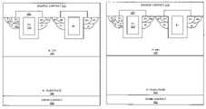
- the FET device 300includes a metal-oxide-semiconductor field effect transistor (MOSFET) having a junction field effect transistor (JFET) embedded as a body diode. More specifically, the FET 300 includes a source contact 310 , a plurality of source regions 315 , a plurality of gate regions 320 , a plurality of gate insulator regions 325 , a plurality of body regions 330 , 335 , a drain region 340 , 345 and a drain contact 350 .
- the drain region 340 , 345may optionally include a first drain region 340 and a second drain region 345 .
- the body regions 330 , 335may optionally include first body regions 330 and second body regions 335 .
- the source regions 315may be formed as parallel elongated structures disposed above the drain region 340 , 345 and proximate the gate regions 320 .
- the body regions 330 , 335may be disposed adjacent the source regions 315 and proximate the gate regions 320 .
- the drain region 340 , 345may be disposed the body regions 330 , 335 and proximate the gate regions 320 . Accordingly, the body regions 330 , 335 are disposed between the source regions 315 and the drain region 340 , 345 .
- the gate regions 320may be formed as parallel elongated structures disposed within the source regions 315 , the body regions 330 , 335 and the drain region 340 , 345 .
- the gate insulator regions 325surround the gate regions 320 .
- the gate regions 320are electrically isolated from the surrounding regions by the gate insulator regions 325 .
- the source contact 310may be disposed on the source regions 315 , the body regions 330 , 335 and the drain regions 340 , 345 . Accordingly, the source contact 310 couples the source regions 315 to the body regions 330 , 335 and corresponding portion of the drain region 340 , 345 disposed between the body regions 330 , 335 .
- the source regions 315 , the drain region 340 and the gate regions 320may be a semiconductor having a first doping type.
- the body regionsmay be a semiconductor having a second doping type.
- the source regions 315 and the drain region 340 , 345may be n-doped semiconductor such as silicon doped with Phosphorus or Arsenic.
- the body regions 330 , 335may be p-doped semiconductor, such as silicon doped with Boron.
- the gate regions 320may be n-doped semiconductor, such as polysilicon doped with Phosphorus.
- the gate insulator regions 325may be an insulator, such as silicon dioxide.
- the source regions 315 and the drain region 340 , 350may be p-doped semiconductor such as silicon doped with Boron.
- the body regions 330 , 335may be n-doped semiconductor, such as silicon doped with Phosphorus or Arsenic.
- the gate regions 320may be p-doped semiconductor, such as polysilicon doped with Phosphorus.
- the gate insulator region 325may be an insulator, such as silicon dioxide.
- the source regions 315may be heavily n-doped (N+) semiconductor, such as silicon doped with Phosphorus or Arsenic.
- the second drain region 345 proximate the drain contact 350may be heavily n-doped (N+) semiconductor, such as silicon doped with Phosphorus or Arsenic.
- the first drain region 340 proximate the body region 330 , 335may be moderately to lightly n-doped (N or N ⁇ ) semiconductor, such as silicon doped with Phosphorus or Arsenic.
- the first body regions 330 disposed between the source regions 315 and the first drain region 340 proximate the gate regions 320may be moderately to lightly p-doped (P or P ⁇ ) semiconductor, such as silicon doped with Boron.
- the second body regions 335 proximate the source contact 310may be heavily p-doped (P+) semiconductor, such as silicon doped with Boron.
- the gate region 320may heavily n-doped (N+) semiconductor, such as polysilicon doped with Phosphorus.
- the gate insulator regions 325may be an insulator, such as silicon dioxide.
- the source contact 310may be a metal or a silicide.
- the source regions 315may be heavily p-doped (P+) semiconductor, such as silicon doped with Boron.
- the second drain region 345 proximate the drain contact 350may be heavily p-doped (P+) semiconductor, such as silicon doped with Boron.
- the first drain region 340 proximate the body region 330 , 335may be moderately to lightly p-doped (P or P ⁇ ) semiconductor, such a silicon doped with Boron.
- the first body regions 330 disposed between the source regions 315 and the first drain region 340 proximate the gate regions 320may be moderately to lightly n-doped (N or N ⁇ ) semiconductor, such as silicon doped with Phosphorus or Arsenic.
- the second body regions 335 proximate the source contact 310may be heavily n-doped (N+) semiconductor, such as silicon doped with Phosphorus or Arsenic.
- the gate region 320may heavily p-doped (P+) semiconductor, such as polysilicon doped with Boron.
- the gate insulator regions 325may be an insulator, such as silicon dioxide.
- the source contact 310may be a metal or a silicide.
- the gate regions 320may be coupled to form a common gate of a trench metal-oxide-semiconductor field effect transistor (TMOSFET).
- the source regions 315may be coupled to form a common source of the TMOSFET.
- the body regions 330 , 335may be coupled to form a common body of the TMOSFET, while the portions of the body region disposed proximate the gate regions 320 form a conducting channel of the TMOSFET.
- the drain region 340 , 345forms the drain of the TMOSFET.
- the portions of the drain region 340 , 345 disposed between the body regions 330 , 335forms a conducting channel of a junction field effect transistor (JFET).
- the body regions 330 , 335form a gate of the JFET.
- the source contact 310 and the drain region 340 , 345form the source and drain of the JFET.
- a Schottky junctionis formed at the interface between the source contact 310 and the drain region 340 , 345 .
- the Schottky junction in combination with the JFETform a gated Schottky diode.
- the gatespinch off the conduction channel during reverse bias, thereby increasing the breakdown voltage of the Schottky junction and reducing the leakage current.
- the Schottky diodeincreases minority carrier injection into the depletion region.
- the resulting body diodeis in effect a merged PiN diode.
- the device 300When the potential of the gate regions 320 , with respect to the source regions 315 , is increased above the threshold voltage of the device 300 , a conducting channel is induced in the body region 330 , 335 along the periphery of the gate insulator regions 325 . The TMOSFET will then conduct current between the drain region 340 , 345 and the source regions 315 . Accordingly, the device is in its on state.
- the TMOSFETWhen the potential of the gate regions 320 is reduced below the threshold voltage, the channel is no longer induced. As a result, a voltage potential applied between the drain region 340 , 345 and the source regions 315 will not cause current to flow there between. Accordingly, the TMOSFET is in its off state and the depletion region formed in the portion of the first drain region 340 , proximate the body regions 330 , 335 supports the voltage applied across the source and drain.
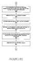
- FIGS. 4A , 4 B, 4 C and 4 Da flow diagram of a method of fabricating a field effect transistor (FET) device, in accordance with one embodiment of the present invention, is shown.
- the methodbegins, at 405 , with various initial processes upon a semiconductor substrate.
- the various initial processesmay include cleaning, depositing, doping, etching and/or the like.
- the semiconductor substratemay contain a first type of dopant at a first concentration.
- the substratemay be silicon, gallium arsenide, indium phosphide or the like, heavily doped with Phosphorus or Arsenic (N+) at a concentration of approximately 1.0E17 cm ⁇ 3 to 1.0E20 cm ⁇ 3 .
- the substratemay be silicon, gallium arsenide, indium phosphide or the like, heavily doped with Boron (P+).
- a semiconductor layermay be epitaxial deposited upon the substrate.
- an epitaxial deposited layerof approximately 30 nano-meters (nm) to 400 nm is formed upon the substrate.
- the epitaxial deposited semiconductor layermay contain the first type of dopant at a second concentration.
- the semiconductor layermay be doped by introducing the dopant into the epitaxial chamber during deposition.
- the epitaxial deposited semiconductor layermay also be doped by an optional high-energy implant and thermal anneal process after deposition.
- the epitaxial deposited semiconductor layermay be silicon, gallium arsenide, indium phosphide or the like, moderately to lightly doped with Phosphorus or Arsenic (N or N ⁇ ) at a concentration of approximately 5.0E14 cm ⁇ 3 to 5.0E16 cm ⁇ 3 .
- the epitaxial deposited semiconductor layermay be silicon, gallium arsenide, indium phosphide or the like, moderately to lightly doped with Boron (P or P ⁇ ).
- a first photo-resistmay be deposited and patterned by any well-known lithography process to define a plurality of body regions.
- a second type of dopantmay be selectively implanted in the portions of the epitaxial deposited semiconductor layer exposed by the patterned first photo-resist to form a first plurality of well regions.
- the dopantmay be implanted utilizing any well-known ion-implant process at a first energy level.
- the first doping processresults in the formation of first well regions having a second dopant at a third concentration.
- the first well regionsmay be moderately to lightly doped with Boron (P or P ⁇ )) at a concentration of approximately 5.0E14 cm ⁇ 3 to 5.0E16 cm ⁇ 3 .
- the first well regionsmay be moderately to lightly doped with Phosphorus or Arsenic (N or N ⁇ ).
- the first wellsform a plurality of lightly to moderately doped body regions of the TMOSFET.
- the second type of dopantmay be selectively implanted in the portions of the epitaxial deposited semiconductor layer exposed by the patterned first photo-resist to form a second plurality of well regions disposed above the first well region.
- the second type of dopantmay be implanted at a second energy level that is less than the first energy level.
- the second doping processresults in the formation of second well regions having the second dopant at fourth concentration.
- the second well regionsmay be heavily doped with Boron (P or P ⁇ ) at a concentration of approximately 5.0E16 cm ⁇ 3 to 1.0E20 cm ⁇ 3 .
- the second well regionsmay be heavily doped with Phosphorus or Arsenic (N or N ⁇ ).
- the second wellsform a plurality of heavily doped body regions of the TMOSFET.
- the first and second well regionsalso form a plurality of gate regions of a JFET.
- the channel of the JFETis formed by a portion of the epitaxial layer disposed between the well regions.
- the first patterned photo-resistis removed utilizing an appropriate resist stripper or resist ashing process.
- a second photo-resistmay be deposited and patterned by any well-known lithography process to define a plurality of source regions disposed within the body regions. The openings in the second pattern photo-resist are smaller than the first and second well regions. The openings in the second patterned photo-resist are aligned to be substantially centered within the first and second well regions. Referring now to FIG.
- the first type of dopantmay be selectively implanted in the portions of the epitaxial deposited semiconductor layer exposed by the patterned second photo-resist to form the third plurality of well regions disposed above the first well regions and within the second well regions, at 440 .
- the dopantmay be implanted at a third energy level.
- the third doping processresults in the formation of third plurality of well regions having the first dopant at a fifth concentration.
- the third well regionsmay be heavily doped with Phosphorus or Arsenic (N+) at a concentration of approximately 1.0E17 cm ⁇ 3 to 1.0E20 cm ⁇ 3 .
- the third well regionsmay be heavily doped with Boron (P+).
- the third wellsform a plurality of source regions of the TMOSFET.
- the second patterned photo-resistis removed utilizing an appropriate resist stripper or resist ashing process.
- a third photo-resistmay be deposited and patterned by any well-known lithography process to define a plurality of gate regions disposed within the source and body regions. The openings in the third patterned photo-resist are smaller than the third plurality of well regions. The openings in the third pattern photo-resist are aligned to be substantially centered within the first, second and third plurality of well regions.
- the portions of the third, second and first well regions exposed by the third patterned photo-resistmay be removed by any well-known etching process. In one implementation, the resulting trenches may extend into the epitaxial deposited layer just below the first well region.
- the third patterned photo-resist layermay be removed utilizing an appropriate resist stripper or resist ashing process.
- a first dielectric layermay be formed in the epitaxial deposited layer proximate the trenches.
- the first dielectric layermay be formed by any well-known oxidation or deposition processes. In one implementation, the dielectric is formed by oxidizing the surface of the silicon proximate the trenches to form a silicon dioxide layer. In one implementation the first dielectric layer may be approximately 15 nm to 200 nm thick. The resulting dielectric along the trench walls forms first port-ion of a plurality of gate insulator regions of the TMOSFET.
- a second semiconductor layermay be deposited in the trenches to form a plurality gate regions of the TMOSFET, at 470 .
- the polysiliconis deposited in the trenches by a method such as decomposition of silane (SiH 4 ).
- the polysiliconmay be doped by introducing the impurity during the deposition process or in a separate doping process.
- the polysiliconmay be heavily doped with Phosphorus or Arsenic (N+) at a concentration of approximately 1.0E17 cm ⁇ 3 to 1.0E20 cm ⁇ 3 .
- the polysiliconmay be heavily doped with Boron (P+).
- P+Boron
- an etch-back processis performed to remove excess polysilicon on the surface of the wafer.
- the excess polysiliconmay be removed utilizing an appropriate etching and/or chemical-mechanical polishing (CMP) process.
- a second dielectric layeris formed on the wafer to complete the gate insulator regions disposed about the gate regions.
- the second dielectric layermay be formed by any well-known oxidation or deposition processes.
- a fourth photo-resistmay be deposited and patterned by any well-known lithography process to define a plurality of source-body contact openings between the gate regions.
- the portions of the second dielectric layer exposed by the fourth patterned photo-resistmay be removed by any well-known etching process.
- the fourth patterned photo-resist layermay be removed utilizing an appropriate resist stripper or resist ashing process.
- a metal layeris deposited on the surface of the wafer, at 488 .
- the deposited metalmay be deposited such that the first, second and third plurality of well regions and a fourth portion of the first semiconductor layer disposed between the second plurality of well regions are electrically coupled to each other.
- the source-body metal layeris deposited by any well-known method such as sputtering.
- the source-body metal layerforms a contact with the body and source regions left exposed by the patterned second dielectric layer.
- the source-body metal layeris isolated from the gate region by the patterned first and second dielectric layers.
- the source-body metal layeralso forms a Schottky barrier at the interface of the epitaxial deposited layer disposed between the first, second and third well regions.
- the metal layermay be titanium, cobalt, platinum, their silicides or the like.
- the metal layeris then patterned utilizing a photo-resist mask and selective etching method to form source-body contact, at 490 .
- fabricationcontinues with various other processes.
- the various processestypically include etching, deposition, doping, cleaning, annealing, passivation, cleaving and/or the like.
- the FET device 500includes a metal-oxide-semiconductor field effect transistor (MOSFET) having a junction field effect transistor (JFET) embedded as a body diode. More specifically, the FET 500 includes a source contact 510 , a plurality of source regions 515 , a plurality of gate regions 520 , a plurality of gate insulator regions 525 , a plurality of body regions 530 , 535 , a drain region 540 , 545 and a drain contact 550 .
- the drain region 540 , 545may optionally include a first drain region 540 and a second drain region 545 .
- the body regions 530 , 535may optionally include first body regions 530 and second body regions 535 .
- the source regions 515may be formed as parallel elongated structure disposed above the drain region 540 , 545 and proximate the gate regions.
- the body regions 530 , 535may be disposed adjacent the source regions 515 and proximate the gate regions 530 , 535 .
- the gate regions 520may be formed disposed above the drain region 540 , 545 and a portion of the body regions 530 , 535 .
- the drain regions 540 , 545may be disposed between the body region 530 , 535 and proximate the gate regions. Accordingly, the body regions 530 , 535 are disposed between the source regions 515 and the drain regions 540 , 545 .
- the gate insulator regions 525surround the gate regions 520 .
- the gate regions 520are electrically isolated from the surrounding regions by the gate insulator regions 525 .
- the source contact 510may be disposed upon the source regions 515 , the body regions 530 , 535 and the drain regions 540 , 545 between the gate regions 520 . Accordingly, the source contact 510 couples the source regions 515 to the body regions 530 , 535 and corresponding portions of the drain region 340 , 345 disposed between the body regions 330 , 335 .
- the source regions 515 , the drain region 540 , 545 and the gate regions 520may be a semiconductor having a first doping type.
- the body regions 530 , 535may be a semiconductor having a second doping type.
- the source regions 515 and the drain region 540 , 545may be n-doped semiconductor such as silicon doped with Phosphorus or Arsenic.
- the body regions 530 , 535may be p-doped semiconductor, such as silicon doped with Boron.
- the gate regions 520may be n-doped semiconductor, such as polysilicon doped with Phosphorus.
- the gate insulator regions 525may be an insulator, such as silicon dioxide.
- the source regions 515 and the drain region 540 , 550may be p-doped semiconductor such as silicon doped with Boron.
- the body regions 530 , 535may be n-doped semiconductor, such as silicon doped with Phosphorus or Arsenic.
- the gate regions 520may be p-doped semiconductor, such as polysilicon doped with Phosphorus.
- the gate insulator region 525may be an insulator, such as silicon dioxide.
- the source regions 515may be heavily n-doped (N+) semiconductor, such as silicon doped with Phosphorus or Arsenic.
- the second drain region 545 proximate the drain contact 550may be heavily n-doped (N+) semiconductor, such as silicon doped with Phosphorus or Arsenic.
- the first drain region 540 proximate the body region 530 , 535may be moderately to lightly n-doped (N or N ⁇ ) semiconductor, such a silicon doped with Phosphorus or Arsenic.
- the first body regions 530 disposed between the source regions 515 and the first drain region 540 proximate the gate regions 520may be moderately to lightly p-doped (P or P ⁇ ) semiconductor, such as silicon doped with Boron.
- the second body regions 535 proximate the source contact 510may be heavily p-doped (P+) semiconductor, such as silicon doped with Boron.
- the gate region 520may heavily n-doped (N+) semiconductor, such as polysilicon doped with Phosphorus.
- the gate insulator regions 525may be an insulator, such as silicon dioxide.
- the source contact 510may be a metal or a silicide.
- the source regions 515may be heavily p-doped (P+) semiconductor, such as silicon doped with Boron.
- the second drain region 545 proximate the drain contact 550may be heavily p-doped (P+) semiconductor, such as silicon doped with Boron.
- the first drain region 540 proximate the body region 530 , 535may be moderately to lightly p-doped (P or P ⁇ ) semiconductor, such a silicon doped with Boron.
- the first body regions 330 disposed between the source regions 515 and the first drain region 540 proximate the gate regions 520may be moderately to lightly n-doped (N or N ⁇ ) semiconductor, such a silicon doped with Phosphorus or Arsenic.
- the second body regions 535 proximate the source contact 510may be heavily n-doped (N+) semiconductor, such as silicon doped with Phosphorus or Arsenic.
- the gate region 520may heavily p-doped (P+) semiconductor, such as polysilicon doped with Boron.
- the gate insulator regions 525may be an insulator, such as silicon dioxide.
- the source contact 510may be a metal or a silicide.
- the gate regions 520may be coupled to form a common gate of a non-trench metal-oxide-semiconductor field effect transistor (MOSFET).
- the source regions 515may be coupled to form a common source of the MOSFET.
- the body regions 530 , 535may be coupled to form a common body of the MOSFET, while the portions of the body region disposed proximate the gate regions 520 form a conducting channel of the MOSFET.
- the drain region 340 , 345forms the drain of the MOSFET.
- the portions of the drain region 540 , 545 disposed between the body regions 530 , 535forms a conducting channel of a junction field effect transistor (JFET).
- the body regions 530 , 535form a gate of the JFET.
- the source contact 510 and the drain region 540 , 545form the source and drain of the JFET.
- a Schottky junctionis formed at the interface between the source contact 510 and the drain region 540 , 545 .
- the Schottky junction in combination with the JFETform a gated Schottky diode.
- the gatespinch off the conduction channel during reverse bias, thereby increasing the breakdown voltage of the Schottky junction and reducing the leakage current.
- the Schottky diodeincreases minority carrier injection into the depletion region.
- the resulting body diodeis in effect a merged PiN diode.
- the MOSFETWhen the potential of the gate regions 520 is reduced below the threshold voltage, the channel is no longer induced. As a result, a voltage potential applied between the drain region 540 , 545 and the source regions 515 will not cause current to flow there between. Accordingly, the MOSFET is in its off state and the depletion region formed in the portion of the first drain region 540 , proximate the body regions 530 , 535 supports the voltage applied across the source and drain.
- FIGS. 6A , 6 B, 6 C and 6 Da flow diagram of a method of fabricating a field effect transistor (FET) device, in accordance with another embodiment of the present invention, is shown.
- the methodbegins, at 605 , with various initial processes upon a semiconductor substrate.
- the various initial processesmay include cleaning, depositing, doping, etching and/or the like.
- the semiconductor substratemay contain a first type of dopant at a first concentration.
- the substratemay be silicon, gallium arsenide, indium phosphide or the like, heavily doped with Phosphorus or Arsenic (N+) at a concentration of approximately 1.0E17 cm ⁇ 3 to 1.0E20 cm ⁇ 3 .
- the substratemay be silicon, gallium arsenide, indium phosphide or the like, heavily doped with Boron (P+).
- a semiconductor layermay be epitaxial deposited upon the substrate.
- an epitaxial deposited layerof approximately 30 nano-meters (nm) to 400 nm is formed upon the substrate.
- the epitaxial deposited semiconductor layermay contain the first type of dopant at a second concentration.
- the semiconductor layermay be doped by introducing the dopant into the epitaxial chamber during deposition.
- the epitaxial deposited semiconductor layermay also be doped by an optional high-energy implant and thermal anneal process after deposition.
- the epitaxial deposited semiconductor layermay be silicon, gallium arsenide, indium phosphide or the like, moderately to lightly doped with Phosphorus or Arsenic (N or N ⁇ ) at a concentration of approximately 5.0E14 cm ⁇ 3 to 5.0E16 cm ⁇ 3 .
- the epitaxial deposited semiconductor layermay be silicon, gallium arsenide, indium phosphide or the like, moderately to lightly doped with Boron (P or P ⁇ ).
- a first photo-resistmay be deposited and patterned by any well-known lithography process to define a plurality of body regions.
- a second type of dopantmay be selectively implanted in the portions of the epitaxial deposited semiconductor layer exposed by the patterned first photo-resist to form a first plurality of well regions.
- the dopantmay be implanted utilizing any well-known ion-implant process at a first energy level.
- the first doping processresults in the formation of first well regions having a second dopant at a third concentration.
- the first well regionsmay be moderately to lightly doped with Boron (P or P ⁇ )) at a concentration of approximately 5.0E14 cm ⁇ 3 to 5.0E16 cm ⁇ 3 .
- the first well regionsmay be moderately to lightly doped with Phosphorus or Arsenic (N or N ⁇ ).
- the first wellsform a plurality of lightly to moderately doped body regions of the MOSFET.
- the first patterned photo-resistis removed utilizing an appropriate resist stripper or resist ashing process.
- a second photo-resistmay be deposited and patterned by any well-known lithography process to define a second plurality of wells disposed within the first plurality of wells.
- the second type of dopantmay be selectively implanted in the portions of the epitaxial deposited semiconductor layer exposed by the patterned second photo-resist to form a second plurality of well regions disposed within the first plurality of well regions.
- the second type of dopantmay be implanted at a second energy level that is less than the first energy level.
- the second doping processresults in the formation of second well regions having the second dopant at fourth concentration.
- the second well regionsmay be heavily doped with Boron (P or P ⁇ ) at a concentration of approximately 5.0E16 cm ⁇ 3 to 1.0E20 cm ⁇ 3 .
- the second well regionsmay be heavily doped with Phosphorus or Arsenic (N or N ⁇ ).
- the second wellsform a plurality of heavily doped body regions of the MOSFET.
- the first and second well regionsalso form a plurality of gate regions of a JFET.
- the channel of the JFETis formed by a portion of the epitaxial deposited layer disposed between the second plurality of well regions.
- a third photo-resistmay be deposited and patterned by any well-known lithography process to define a plurality of a third set of wells disposed within the first set of wells.
- the openings in the third pattern photo-resistare smaller than the first and second well regions.
- the openings in the third patterned photo-resistare aligned to be substantially centered within the first plurality of well regions.
- the first type of dopantmay be selectively implanted in the portions of the epitaxial deposited semiconductor layer exposed by the patterned third photo-resist to form a third plurality of well regions disposed within the first and second well regions.
- the dopantmay be implanted at a third energy level.
- the third doping processresults in the formation of third well regions having the first dopant at a fifth concentration.
- the third well regionsmay be heavily doped with Phosphorus or Arsenic (N+) at a concentration of approximately 1.0E17 cm ⁇ 3 to 1.0E20 cm ⁇ 3 cm.
- the third well regionsmay be heavily doped with Boron (P+).
- the third wellsform a plurality of source regions of the MOSFET.
- a first dielectric layermay be formed on the wafer.
- the first dielectric layermay be formed by any well-known oxidation or deposition processes.
- the dielectricis formed by oxidizing the surface of the silicon wafer to form a silicon dioxide layer.
- the first dielectric layermay be approximately 15 nm to 200 nm thick. The resulting dielectric forms a portion of a plurality of gate insulator regions of the MOSFET upon a fourth portion of the first semiconductor layer proximate the first plurality of well regions.
- a polysilicon layeris deposited on the first dielectric layer.
- the polysiliconis deposited by a method such as decomposition of silane (SiH 4 ).
- the polysiliconmay be doped by introducing the impurity during the deposition process or in a separate doping process.
- the polysiliconmay be heavily doped with Phosphorus or Arsenic (N+) at a concentration of approximately 1.0E17 cm ⁇ 3 to 1.0E20 cm ⁇ 3 .
- the polysiliconmay be heavily doped with Boron (P+).
- a fourth photo-resistmay be deposited and patterned by any well-known lithography process to define the gate regions.
- the portions of the first dielectric layer, polysilicon layer and second dielectric layer exposed by the fourth patterned photo-resistmay be removed by any well-known etching process, at 660 .
- the fourth patterned photo-resist layermay be removed utilizing an appropriate resist stripper or resist ashing process.
- a second dielectric layeris on the wafer.
- the second dielectric layercompletes the gate insulator regions disposed about the gate regions.
- the second dielectric layermay be formed by any well-known oxidation processes.
- a fifth photo-resistmay be deposited and patterned by any well-known lithography process to define a plurality of source-body contact openings between the gate regions.
- the portions of the second dielectric layer exposed by the fifth patterned photo-resistmay be removed by any well-known etching process.
- the fifth patterned photo-resist layermay be removed utilizing an appropriate resist stripper or resist ashing process.
- a source-body metal layeris deposited on the surface of the wafer, at 684 .
- the source-body metal layermay be deposited such that the first second and third plurality of well regions and a fourth portion of the first semiconductor layer disposed between the second plurality of well regions are electrically coupled to each other.
- the source-body metal layeris deposited by any well-known method such as sputtering.
- the source-body metal layerforms a contact with the body and source regions left exposed by the patterned second dielectric layer.
- the source-body metal layeris isolated from the gate region by the patterned first second and third dielectric layers.
- the source-body metal layeralso forms a Schottky barrier at the interface of the epitaxial deposited layer disposed between the first, second and third well regions.
- the source-body metal layeris then patterned utilizing a photo-resist mask and selective etching method as needed, at 686 .
- fabricationcontinues with various other processes.
- the various processestypically include etching, deposition, doping, cleaning, annealing, passivation, cleaving and/or the like.
- JFET devicesprovide JFET devices having reduced leakage current and/or faster switching, as compared to conventional power MOSFET devices.
- the JFET devices having reduced leakage current and/or faster switching characteristicsmay advantageously be utilized in many applications such as high-frequency DC-DC converters and the like.
Landscapes
- Insulated Gate Type Field-Effect Transistor (AREA)
Abstract
Description
Claims (18)
Priority Applications (3)
| Application Number | Priority Date | Filing Date | Title |
|---|---|---|---|
| US11/149,718US7417266B1 (en) | 2004-06-10 | 2005-06-10 | MOSFET having a JFET embedded as a body diode |
| US12/182,365US8097512B2 (en) | 2004-06-10 | 2008-07-30 | MOSFET having a JFET embedded as a body diode |
| US13/136,986US8916929B2 (en) | 2004-06-10 | 2011-08-16 | MOSFET having a JFET embedded as a body diode |
Applications Claiming Priority (2)
| Application Number | Priority Date | Filing Date | Title |
|---|---|---|---|
| US57902004P | 2004-06-10 | 2004-06-10 | |
| US11/149,718US7417266B1 (en) | 2004-06-10 | 2005-06-10 | MOSFET having a JFET embedded as a body diode |
Related Child Applications (1)
| Application Number | Title | Priority Date | Filing Date |
|---|---|---|---|
| US12/182,365ContinuationUS8097512B2 (en) | 2004-06-10 | 2008-07-30 | MOSFET having a JFET embedded as a body diode |
Publications (1)
| Publication Number | Publication Date |
|---|---|
| US7417266B1true US7417266B1 (en) | 2008-08-26 |
Family
ID=39711225
Family Applications (3)
| Application Number | Title | Priority Date | Filing Date |
|---|---|---|---|
| US11/149,718Expired - Fee RelatedUS7417266B1 (en) | 2004-06-10 | 2005-06-10 | MOSFET having a JFET embedded as a body diode |
| US12/182,365Expired - Fee RelatedUS8097512B2 (en) | 2004-06-10 | 2008-07-30 | MOSFET having a JFET embedded as a body diode |
| US13/136,986Expired - Fee RelatedUS8916929B2 (en) | 2004-06-10 | 2011-08-16 | MOSFET having a JFET embedded as a body diode |
Family Applications After (2)
| Application Number | Title | Priority Date | Filing Date |
|---|---|---|---|
| US12/182,365Expired - Fee RelatedUS8097512B2 (en) | 2004-06-10 | 2008-07-30 | MOSFET having a JFET embedded as a body diode |
| US13/136,986Expired - Fee RelatedUS8916929B2 (en) | 2004-06-10 | 2011-08-16 | MOSFET having a JFET embedded as a body diode |
Country Status (1)
| Country | Link |
|---|---|
| US (3) | US7417266B1 (en) |
Cited By (27)
| Publication number | Priority date | Publication date | Assignee | Title |
|---|---|---|---|---|
| US20060273400A1 (en)* | 2005-06-01 | 2006-12-07 | Hitachi, Ltd. | High voltage analog switch ICS and ultrasound imaging systems using same |
| US20070187717A1 (en)* | 2005-05-13 | 2007-08-16 | Coldwatt, Inc. | Semiconductor device having reduced on-resistance and method of forming the same |
| US20070298559A1 (en)* | 2006-06-21 | 2007-12-27 | Brar Berinder P S | Vertical Field-Effect Transistor and Method of Forming the Same |
| US20070298564A1 (en)* | 2006-06-21 | 2007-12-27 | Brar Berinder P S | Vertical Field-Effect Transistor and Method of Forming the Same |
| US20080048174A1 (en)* | 2005-08-25 | 2008-02-28 | Sadaka Mariam G | Semiconductor Device Including a Lateral Field-Effect Transistor and Schottky Diode |
| US20080157060A1 (en)* | 2005-05-13 | 2008-07-03 | Brar Berinder P S | Semiconductor Device Having Multiple Lateral Channels and Method of Forming the Same |
| US20080217721A1 (en)* | 2007-03-09 | 2008-09-11 | Hamerski Roman J | High efficiency rectifier |
| US20080265396A1 (en)* | 2006-05-23 | 2008-10-30 | International Business Machines Corporation | Quad flat no-lead chip carrier with standoff |
| US20090236660A1 (en)* | 2006-12-04 | 2009-09-24 | Sanken Electric Co., Ltd. | Insulated-Gate Field-Effect Transistor and Method of Making the Same |
| US20090273023A1 (en)* | 2007-02-16 | 2009-11-05 | Power Integrations, Inc. | Segmented pillar layout for a high-voltage vertical transistor |
| US20090278176A1 (en)* | 2008-05-12 | 2009-11-12 | Vishay-Siliconix | High current density power field effect transistor |
| US20090315105A1 (en)* | 2007-02-16 | 2009-12-24 | Power Integrations, Inc. | High-voltage vertical transistor structure |
| US20100032711A1 (en)* | 2008-08-11 | 2010-02-11 | Mitsubishi Electric Corporation | Semiconductor device and method of manufacturing the same |
| US20110073938A1 (en)* | 2008-06-02 | 2011-03-31 | Sanken Electric Co., Ltd. | Field-effect semiconductor device and method of producing the same |
| US20110079819A1 (en)* | 2009-10-06 | 2011-04-07 | Wei-Chieh Lin | Igbt with fast reverse recovery time rectifier and manufacturing method thereof |
| US20130026568A1 (en)* | 2005-02-11 | 2013-01-31 | Anup Bhalla | Planar srfet using no additional masks and layout method |
| US8410551B2 (en) | 2007-02-16 | 2013-04-02 | Power Integrations, Inc. | Checkerboarded high-voltage vertical transistor layout |
| US8633094B2 (en) | 2011-12-01 | 2014-01-21 | Power Integrations, Inc. | GaN high voltage HFET with passivation plus gate dielectric multilayer structure |
| US8653583B2 (en) | 2007-02-16 | 2014-02-18 | Power Integrations, Inc. | Sensing FET integrated with a high-voltage transistor |
| US8916929B2 (en) | 2004-06-10 | 2014-12-23 | Power Integrations, Inc. | MOSFET having a JFET embedded as a body diode |
| US8928037B2 (en) | 2013-02-28 | 2015-01-06 | Power Integrations, Inc. | Heterostructure power transistor with AlSiN passivation layer |
| US8940620B2 (en) | 2011-12-15 | 2015-01-27 | Power Integrations, Inc. | Composite wafer for fabrication of semiconductor devices |
| US9543396B2 (en) | 2013-12-13 | 2017-01-10 | Power Integrations, Inc. | Vertical transistor device structure with cylindrically-shaped regions |
| US9911840B2 (en)* | 2010-12-14 | 2018-03-06 | Alpha And Omega Semiconductor Incorporated | Self aligned trench MOSFET with integrated diode |
| US10312260B2 (en) | 2013-07-29 | 2019-06-04 | Efficient Power Conversion Corporation | GaN transistors with polysilicon layers used for creating additional components |
| US10325988B2 (en) | 2013-12-13 | 2019-06-18 | Power Integrations, Inc. | Vertical transistor device structure with cylindrically-shaped field plates |
| US20200335496A1 (en)* | 2019-04-18 | 2020-10-22 | Mitsubishi Electric Corporation | Semiconductor device |
Families Citing this family (8)
| Publication number | Priority date | Publication date | Assignee | Title |
|---|---|---|---|---|
| US8115457B2 (en) | 2009-07-31 | 2012-02-14 | Power Integrations, Inc. | Method and apparatus for implementing a power converter input terminal voltage discharge circuit |
| US8207577B2 (en)* | 2009-09-29 | 2012-06-26 | Power Integrations, Inc. | High-voltage transistor structure with reduced gate capacitance |
| JP5310687B2 (en)* | 2010-09-30 | 2013-10-09 | 株式会社デンソー | Semiconductor device provided with junction field effect transistor and manufacturing method thereof |
| EP3005419A4 (en)* | 2013-06-06 | 2017-03-15 | United Silicon Carbide Inc. | Trench shield connected jfet |
| US9583482B2 (en) | 2015-02-11 | 2017-02-28 | Monolith Semiconductor Inc. | High voltage semiconductor devices and methods of making the devices |
| JP6514035B2 (en)* | 2015-05-27 | 2019-05-15 | 株式会社豊田中央研究所 | Semiconductor device |
| US12310048B2 (en)* | 2022-04-08 | 2025-05-20 | Hong Kong Applied Science and Technology Research Institute Company Limited | Silicon-carbide (SiC) metal-oxide-semiconductor field-effect transistor (MOSFET) with short circuit protection |
| KR20240057165A (en) | 2022-10-24 | 2024-05-02 | 현대자동차주식회사 | Power semiconductor device |
Citations (8)
| Publication number | Priority date | Publication date | Assignee | Title |
|---|---|---|---|---|
| US4967243A (en)* | 1988-07-19 | 1990-10-30 | General Electric Company | Power transistor structure with high speed integral antiparallel Schottky diode |
| US5689128A (en)* | 1995-08-21 | 1997-11-18 | Siliconix Incorporated | High density trenched DMOS transistor |
| US20010001494A1 (en)* | 1999-04-01 | 2001-05-24 | Christopher B. Kocon | Power trench mos-gated device and process for forming same |
| US6809375B2 (en)* | 2001-04-02 | 2004-10-26 | Shindengen Electric Manufacturing Co., Ltd. | Semiconductor device having shallow trenches and method for manufacturing the same |
| US20050215012A1 (en)* | 1999-05-25 | 2005-09-29 | Advanced Analogic Technologies, Inc. | Trench semiconductor device having gate oxide layer with multiple thicknesses and processes of fabricating the same |
| US7084456B2 (en)* | 1999-05-25 | 2006-08-01 | Advanced Analogic Technologies, Inc. | Trench MOSFET with recessed clamping diode using graded doping |
| US7109551B2 (en)* | 2003-08-29 | 2006-09-19 | Fuji Electric Holdings Co., Ltd. | Semiconductor device |
| US7118970B2 (en)* | 2004-06-22 | 2006-10-10 | Cree, Inc. | Methods of fabricating silicon carbide devices with hybrid well regions |
Family Cites Families (126)
| Publication number | Priority date | Publication date | Assignee | Title |
|---|---|---|---|---|
| NL167277C (en) | 1970-08-29 | 1981-11-16 | Philips Nv | SEMICONDUCTOR DEVICE WITH SHEET-FORMING SEMICONDUCTOR BODY WITH AT LEAST PART OF THE THICKNESS OF THE SEMICONDUCTOR BODY EQUIPPED WITH A METAL ELECTRODE THROUGH A CORRECTED VERSION IN A CORRECTED VERSION. |
| US4142195A (en) | 1976-03-22 | 1979-02-27 | Rca Corporation | Schottky barrier semiconductor device and method of making same |
| US4408216A (en) | 1978-06-02 | 1983-10-04 | International Rectifier Corporation | Schottky device and method of manufacture using palladium and platinum intermetallic alloys and titanium barrier for low reverse leakage over wide temperature range |
| NL184551C (en)* | 1978-07-24 | 1989-08-16 | Philips Nv | FIELD-EFFECT TRANSISTOR WITH INSULATED HANDLEBAR ELECTRODE. |
| FR2517883A1 (en) | 1981-12-09 | 1983-06-10 | Thomson Csf | SEMICONDUCTOR DEVICE WITH LOW PARASITE CAPACITY PROVIDED WITH EXTERNAL CONNECTIONS TAKEN WITH BEAMS |
| US4543595A (en) | 1982-05-20 | 1985-09-24 | Fairchild Camera And Instrument Corporation | Bipolar memory cell |
| GB2137412B (en) | 1983-03-15 | 1987-03-04 | Standard Telephones Cables Ltd | Semiconductor device |
| US4946547A (en) | 1989-10-13 | 1990-08-07 | Cree Research, Inc. | Method of preparing silicon carbide surfaces for crystal growth |
| US5200022A (en) | 1990-10-03 | 1993-04-06 | Cree Research, Inc. | Method of improving mechanically prepared substrate surfaces of alpha silicon carbide for deposition of beta silicon carbide thereon and resulting product |
| WO1992016966A1 (en) | 1991-03-18 | 1992-10-01 | Boston University | A method for the preparation and doping of highly insulating monocrystalline gallium nitride thin films |
| US5221413A (en) | 1991-04-24 | 1993-06-22 | At&T Bell Laboratories | Method for making low defect density semiconductor heterostructure and devices made thereby |
| WO1994003931A1 (en) | 1992-08-07 | 1994-02-17 | Asahi Kasei Kogyo Kabushiki Kaisha | Nitride based semiconductor device and manufacture thereof |
| EP0622858B2 (en) | 1993-04-28 | 2004-09-29 | Nichia Corporation | Gallium nitride-based III-V group compound semiconductor device and method of producing the same |
| JP3495814B2 (en) | 1994-05-30 | 2004-02-09 | キヤノン株式会社 | Battery electrode and lithium secondary battery having the electrode |
| EP1339116A3 (en) | 1994-05-30 | 2005-03-23 | Canon Kabushiki Kaisha | Rechargeable lithium battery |
| US6078090A (en) | 1997-04-02 | 2000-06-20 | Siliconix Incorporated | Trench-gated Schottky diode with integral clamping diode |
| WO1996041906A1 (en) | 1995-06-13 | 1996-12-27 | Advanced Technology Materials, Inc. | Bulk single crystal gallium nitride and method of making same |
| US5874747A (en) | 1996-02-05 | 1999-02-23 | Advanced Technology Materials, Inc. | High brightness electroluminescent device emitting in the green to ultraviolet spectrum and method of making the same |
| JP3742144B2 (en) | 1996-05-08 | 2006-02-01 | ソニー株式会社 | Nonaqueous electrolyte secondary battery and planar current collector for nonaqueous electrolyte secondary battery |
| US5612567A (en) | 1996-05-13 | 1997-03-18 | North Carolina State University | Schottky barrier rectifiers and methods of forming same |
| US5741724A (en) | 1996-12-27 | 1998-04-21 | Motorola | Method of growing gallium nitride on a spinel substrate |
| JP3491492B2 (en) | 1997-04-09 | 2004-01-26 | 松下電器産業株式会社 | Method for producing gallium nitride crystal |
| US5785606A (en) | 1997-05-02 | 1998-07-28 | Marquez; Ruben L. | Method of playing multiple hand card game |
| US6239033B1 (en) | 1998-05-28 | 2001-05-29 | Sony Corporation | Manufacturing method of semiconductor device |
| DE19723176C1 (en) | 1997-06-03 | 1998-08-27 | Daimler Benz Ag | Semiconductor device with alternate p-n and Schottky junctions |
| JP2002510275A (en) | 1997-07-03 | 2002-04-02 | シービーエル テクノロジーズ | Removal of defects in epitaxial layers |
| JP3505357B2 (en) | 1997-07-16 | 2004-03-08 | 株式会社東芝 | Gallium nitride based semiconductor device and method of manufacturing the same |
| JP4453111B2 (en) | 1997-10-27 | 2010-04-21 | 三菱化学株式会社 | Negative electrode material and method for producing the same, negative electrode active material, and non-aqueous secondary battery |
| JP3500281B2 (en) | 1997-11-05 | 2004-02-23 | 株式会社東芝 | Gallium nitride based semiconductor device and method of manufacturing the same |
| JP3036495B2 (en) | 1997-11-07 | 2000-04-24 | 豊田合成株式会社 | Method for manufacturing gallium nitride-based compound semiconductor |
| US6608327B1 (en) | 1998-02-27 | 2003-08-19 | North Carolina State University | Gallium nitride semiconductor structure including laterally offset patterned layers |
| JP2948205B1 (en) | 1998-05-25 | 1999-09-13 | 花王株式会社 | Method for producing negative electrode for secondary battery |
| JP4352473B2 (en) | 1998-06-26 | 2009-10-28 | ソニー株式会社 | Manufacturing method of semiconductor device |
| JP2000150535A (en) | 1998-11-09 | 2000-05-30 | Fujitsu Quantum Device Kk | Field effect transistor and method of manufacturing the same |
| US6331450B1 (en) | 1998-12-22 | 2001-12-18 | Toyoda Gosei Co., Ltd. | Method of manufacturing semiconductor device using group III nitride compound |
| US6252288B1 (en) | 1999-01-19 | 2001-06-26 | Rockwell Science Center, Llc | High power trench-based rectifier with improved reverse breakdown characteristic |
| US6389051B1 (en) | 1999-04-09 | 2002-05-14 | Xerox Corporation | Structure and method for asymmetric waveguide nitride laser diode |
| US6252258B1 (en) | 1999-08-10 | 2001-06-26 | Rockwell Science Center Llc | High power rectifier |
| US6211018B1 (en)* | 1999-08-14 | 2001-04-03 | Electronics And Telecommunications Research Institute | Method for fabricating high density trench gate type power device |
| JP4412827B2 (en) | 1999-08-20 | 2010-02-10 | シャープ株式会社 | Nitride semiconductor thick film substrate |
| CN1189958C (en) | 1999-10-22 | 2005-02-16 | 三洋电机株式会社 | Method for producing electrode for lithium secondary cell |
| JP2002083594A (en) | 1999-10-22 | 2002-03-22 | Sanyo Electric Co Ltd | Electrode for lithium battery, lithium battery using it and lithium secondary battery |
| KR100536160B1 (en) | 1999-10-22 | 2005-12-14 | 산요덴키가부시키가이샤 | Electrode for lithium cell and lithium secondary cell |
| US6184570B1 (en) | 1999-10-28 | 2001-02-06 | Ericsson Inc. | Integrated circuit dies including thermal stress reducing grooves and microelectronic packages utilizing the same |
| AU2430401A (en) | 1999-12-13 | 2001-06-18 | North Carolina State University | Methods of fabricating gallium nitride layers on textured silicon substrates, and gallium nitride semiconductor structures fabricated thereby |
| US6380108B1 (en) | 1999-12-21 | 2002-04-30 | North Carolina State University | Pendeoepitaxial methods of fabricating gallium nitride semiconductor layers on weak posts, and gallium nitride semiconductor structures fabricated thereby |
| US6573537B1 (en) | 1999-12-22 | 2003-06-03 | Lumileds Lighting, U.S., Llc | Highly reflective ohmic contacts to III-nitride flip-chip LEDs |
| US6586781B2 (en) | 2000-02-04 | 2003-07-01 | Cree Lighting Company | Group III nitride based FETs and HEMTs with reduced trapping and method for producing the same |
| KR100348269B1 (en) | 2000-03-22 | 2002-08-09 | 엘지전자 주식회사 | Schottky Contact Method Using Ruthenium Oxide |
| JP2001357855A (en) | 2000-06-14 | 2001-12-26 | Shin Kobe Electric Mach Co Ltd | Non-aqueous electrolyte secondary battery |
| US6344665B1 (en) | 2000-06-23 | 2002-02-05 | Arima Optoelectronics Corp. | Electrode structure of compound semiconductor device |
| US20020015833A1 (en) | 2000-06-29 | 2002-02-07 | Naotomi Takahashi | Manufacturing method of electrodeposited copper foil and electrodeposited copper foil |
| JP4022708B2 (en) | 2000-06-29 | 2007-12-19 | 日本電気株式会社 | Semiconductor device |
| JP2003101036A (en) | 2001-09-25 | 2003-04-04 | Sanyo Electric Co Ltd | Schottky barrier diode and method of manufacturing the same |
| JP2002064201A (en) | 2000-08-18 | 2002-02-28 | Toshiba Corp | Semiconductor field effect transistor and power amplifier |
| US6518079B2 (en) | 2000-12-20 | 2003-02-11 | Lumileds Lighting, U.S., Llc | Separation method for gallium nitride devices on lattice-mismatched substrates |
| JP2002305309A (en) | 2001-02-01 | 2002-10-18 | Hitachi Ltd | Semiconductor device and manufacturing method thereof |
| US6437374B1 (en) | 2001-05-07 | 2002-08-20 | Xerox Corporation | Semiconductor device and method of forming a semiconductor device |
| US6998678B2 (en)* | 2001-05-17 | 2006-02-14 | Infineon Technologies Ag | Semiconductor arrangement with a MOS-transistor and a parallel Schottky-diode |
| TW492202B (en) | 2001-06-05 | 2002-06-21 | South Epitaxy Corp | Structure of III-V light emitting diode (LED) arranged in flip chip configuration having structure for preventing electrostatic discharge |
| US20030015708A1 (en) | 2001-07-23 | 2003-01-23 | Primit Parikh | Gallium nitride based diodes with low forward voltage and low reverse current operation |
| US7230284B2 (en) | 2001-07-24 | 2007-06-12 | Cree, Inc. | Insulating gate AlGaN/GaN HEMT |
| US6524900B2 (en) | 2001-07-25 | 2003-02-25 | Abb Research, Ltd | Method concerning a junction barrier Schottky diode, such a diode and use thereof |
| US20050179106A1 (en) | 2001-07-27 | 2005-08-18 | Sanyo Electric Company, Ltd. | Schottky barrier diode |
| JP4064085B2 (en) | 2001-10-18 | 2008-03-19 | 三菱電機株式会社 | Semiconductor device and manufacturing method thereof |
| US6768146B2 (en) | 2001-11-27 | 2004-07-27 | The Furukawa Electric Co., Ltd. | III-V nitride semiconductor device, and protection element and power conversion apparatus using the same |
| JP3871607B2 (en) | 2001-12-14 | 2007-01-24 | 松下電器産業株式会社 | Semiconductor device and manufacturing method thereof |
| US6515308B1 (en) | 2001-12-21 | 2003-02-04 | Xerox Corporation | Nitride-based VCSEL or light emitting diode with p-n tunnel junction current injection |
| US6855970B2 (en) | 2002-03-25 | 2005-02-15 | Kabushiki Kaisha Toshiba | High-breakdown-voltage semiconductor device |
| US6624444B1 (en) | 2002-03-28 | 2003-09-23 | Intel Corporation | Electrical-optical package with capacitor DC shunts and associated methods |
| DE10217235A1 (en) | 2002-04-18 | 2003-10-30 | Philips Intellectual Property | Circuit arrangement for generating DC voltages |
| JP4221697B2 (en) | 2002-06-17 | 2009-02-12 | 日本電気株式会社 | Semiconductor device |
| US7323402B2 (en) | 2002-07-11 | 2008-01-29 | International Rectifier Corporation | Trench Schottky barrier diode with differential oxide thickness |
| JP3790500B2 (en) | 2002-07-16 | 2006-06-28 | ユーディナデバイス株式会社 | Field effect transistor and manufacturing method thereof |
| US20040021152A1 (en) | 2002-08-05 | 2004-02-05 | Chanh Nguyen | Ga/A1GaN Heterostructure Field Effect Transistor with dielectric recessed gate |
| JP2004087587A (en) | 2002-08-23 | 2004-03-18 | Mitsubishi Electric Corp | Nitride semiconductor device and method of manufacturing the same |
| FR2844099B1 (en) | 2002-09-03 | 2005-09-02 | Commissariat Energie Atomique | SEMICONDUCTOR DEVICE OF QUASI-VERTICAL POWER ON COMPOSITE SUBSTRATE |
| US7115896B2 (en) | 2002-12-04 | 2006-10-03 | Emcore Corporation | Semiconductor structures for gallium nitride-based devices |
| JP4748498B2 (en) | 2002-12-05 | 2011-08-17 | 古河電気工業株式会社 | GaN-based semiconductor device with current breaker |
| TWI240434B (en) | 2003-06-24 | 2005-09-21 | Osram Opto Semiconductors Gmbh | Method to produce semiconductor-chips |
| FR2857982B1 (en) | 2003-07-24 | 2007-05-18 | Soitec Silicon On Insulator | PROCESS FOR PRODUCING AN EPITAXIC LAYER |
| US7026665B1 (en) | 2003-09-19 | 2006-04-11 | Rf Micro Devices, Inc. | High voltage GaN-based transistor structure |
| US7041579B2 (en) | 2003-10-22 | 2006-05-09 | Northrop Grumman Corporation | Hard substrate wafer sawing process |
| JP2005129696A (en) | 2003-10-23 | 2005-05-19 | Matsushita Electric Ind Co Ltd | Semiconductor device and manufacturing method thereof |
| JP4288592B2 (en) | 2004-01-20 | 2009-07-01 | ソニー株式会社 | battery |
| JP4449467B2 (en) | 2004-01-28 | 2010-04-14 | サンケン電気株式会社 | Semiconductor device |
| US7253015B2 (en) | 2004-02-17 | 2007-08-07 | Velox Semiconductor Corporation | Low doped layer for nitride-based semiconductor device |
| US7084475B2 (en) | 2004-02-17 | 2006-08-01 | Velox Semiconductor Corporation | Lateral conduction Schottky diode with plural mesas |
| JP4610207B2 (en) | 2004-02-24 | 2011-01-12 | 三洋電機株式会社 | Semiconductor device and manufacturing method thereof |
| US7229866B2 (en) | 2004-03-15 | 2007-06-12 | Velox Semiconductor Corporation | Non-activated guard ring for semiconductor devices |
| EP1749308A4 (en) | 2004-04-28 | 2011-12-28 | Verticle Inc | SEMICONDUCTOR DEVICES WITH VERTICAL STRUCTURE |
| JP4398780B2 (en) | 2004-04-30 | 2010-01-13 | 古河電気工業株式会社 | GaN-based semiconductor device |
| US7417266B1 (en) | 2004-06-10 | 2008-08-26 | Qspeed Semiconductor Inc. | MOSFET having a JFET embedded as a body diode |
| US7238976B1 (en) | 2004-06-15 | 2007-07-03 | Qspeed Semiconductor Inc. | Schottky barrier rectifier and method of manufacturing the same |
| US7547928B2 (en) | 2004-06-30 | 2009-06-16 | Interuniversitair Microelektronica Centrum (Imec) | AlGaN/GaN high electron mobility transistor devices |
| EP2273553B1 (en) | 2004-06-30 | 2020-02-12 | IMEC vzw | A method for fabricating AlGaN/GaN HEMT devices |
| JP2006100645A (en) | 2004-09-30 | 2006-04-13 | Furukawa Electric Co Ltd:The | GaN-based semiconductor integrated circuit |
| US7456443B2 (en) | 2004-11-23 | 2008-11-25 | Cree, Inc. | Transistors having buried n-type and p-type regions beneath the source region |
| JP4609048B2 (en) | 2004-11-25 | 2011-01-12 | ソニー株式会社 | Negative electrode for secondary battery and secondary battery |
| US7116567B2 (en) | 2005-01-05 | 2006-10-03 | Velox Semiconductor Corporation | GaN semiconductor based voltage conversion device |
| US7436039B2 (en) | 2005-01-06 | 2008-10-14 | Velox Semiconductor Corporation | Gallium nitride semiconductor device |
| US20060151868A1 (en) | 2005-01-10 | 2006-07-13 | Zhu Tinggang | Package for gallium nitride semiconductor devices |
| US7429534B2 (en) | 2005-02-22 | 2008-09-30 | Sensor Electronic Technology, Inc. | Etching a nitride-based heterostructure |
| JP2006245317A (en) | 2005-03-03 | 2006-09-14 | Fujitsu Ltd | Semiconductor device and manufacturing method thereof |
| DE102005012217B4 (en) | 2005-03-15 | 2007-02-22 | Infineon Technologies Austria Ag | Lateral MISFET and method of making the same |
| US7615774B2 (en) | 2005-04-29 | 2009-11-10 | Cree.Inc. | Aluminum free group III-nitride based high electron mobility transistors |
| EP1938385B1 (en) | 2005-09-07 | 2014-12-03 | Cree, Inc. | Transistors with fluorine treatment |
| US8026568B2 (en) | 2005-11-15 | 2011-09-27 | Velox Semiconductor Corporation | Second Schottky contact metal layer to improve GaN Schottky diode performance |
| US7696598B2 (en) | 2005-12-27 | 2010-04-13 | Qspeed Semiconductor Inc. | Ultrafast recovery diode |
| WO2007075996A2 (en) | 2005-12-27 | 2007-07-05 | Qspeed Semiconductor Inc. | Apparatus and method for a fast recovery rectifier structure |
| JP4705482B2 (en) | 2006-01-27 | 2011-06-22 | パナソニック株式会社 | Transistor |
| JP5231719B2 (en) | 2006-03-30 | 2013-07-10 | 富士通株式会社 | Method for manufacturing field effect transistor |
| JP5032145B2 (en) | 2006-04-14 | 2012-09-26 | 株式会社東芝 | Semiconductor device |
| US8399911B2 (en) | 2006-06-07 | 2013-03-19 | Imec | Enhancement mode field effect device and the method of production thereof |
| US7939853B2 (en) | 2007-03-20 | 2011-05-10 | Power Integrations, Inc. | Termination and contact structures for a high voltage GaN-based heterojunction transistor |
| JP5462161B2 (en) | 2007-07-20 | 2014-04-02 | アイメック | Method for manufacturing damascene contact in III-V group MESFET |
| US20090278233A1 (en) | 2007-07-26 | 2009-11-12 | Pinnington Thomas Henry | Bonded intermediate substrate and method of making same |
| US8309987B2 (en) | 2008-07-15 | 2012-11-13 | Imec | Enhancement mode semiconductor device |
| US7985986B2 (en) | 2008-07-31 | 2011-07-26 | Cree, Inc. | Normally-off semiconductor devices |
| KR101233105B1 (en) | 2008-08-27 | 2013-02-15 | 소이텍 | Methods of fabricating semiconductor structures or devices using layers of semiconductor material having selected or controlled lattice parameters |
| US8168486B2 (en) | 2009-06-24 | 2012-05-01 | Intersil Americas Inc. | Methods for manufacturing enhancement-mode HEMTs with self-aligned field plate |
| US9306050B2 (en) | 2009-06-26 | 2016-04-05 | Cornell University | III-V semiconductor structures including aluminum-silicon nitride passivation |
| US8791034B2 (en) | 2009-06-26 | 2014-07-29 | Cornell University | Chemical vapor deposition process for aluminum silicon nitride |
| EP2317542B1 (en) | 2009-10-30 | 2018-05-23 | IMEC vzw | Semiconductor device and method of manufacturing thereof |
| JP5635803B2 (en) | 2010-05-07 | 2014-12-03 | トランスフォーム・ジャパン株式会社 | Compound semiconductor device manufacturing method and compound semiconductor device |
| US9070758B2 (en) | 2011-06-20 | 2015-06-30 | Imec | CMOS compatible method for manufacturing a HEMT device and the HEMT device thereof |
- 2005
- 2005-06-10USUS11/149,718patent/US7417266B1/ennot_activeExpired - Fee Related
- 2008
- 2008-07-30USUS12/182,365patent/US8097512B2/ennot_activeExpired - Fee Related
- 2011
- 2011-08-16USUS13/136,986patent/US8916929B2/ennot_activeExpired - Fee Related
Patent Citations (8)
| Publication number | Priority date | Publication date | Assignee | Title |
|---|---|---|---|---|
| US4967243A (en)* | 1988-07-19 | 1990-10-30 | General Electric Company | Power transistor structure with high speed integral antiparallel Schottky diode |
| US5689128A (en)* | 1995-08-21 | 1997-11-18 | Siliconix Incorporated | High density trenched DMOS transistor |
| US20010001494A1 (en)* | 1999-04-01 | 2001-05-24 | Christopher B. Kocon | Power trench mos-gated device and process for forming same |
| US20050215012A1 (en)* | 1999-05-25 | 2005-09-29 | Advanced Analogic Technologies, Inc. | Trench semiconductor device having gate oxide layer with multiple thicknesses and processes of fabricating the same |
| US7084456B2 (en)* | 1999-05-25 | 2006-08-01 | Advanced Analogic Technologies, Inc. | Trench MOSFET with recessed clamping diode using graded doping |
| US6809375B2 (en)* | 2001-04-02 | 2004-10-26 | Shindengen Electric Manufacturing Co., Ltd. | Semiconductor device having shallow trenches and method for manufacturing the same |
| US7109551B2 (en)* | 2003-08-29 | 2006-09-19 | Fuji Electric Holdings Co., Ltd. | Semiconductor device |
| US7118970B2 (en)* | 2004-06-22 | 2006-10-10 | Cree, Inc. | Methods of fabricating silicon carbide devices with hybrid well regions |
Cited By (43)
| Publication number | Priority date | Publication date | Assignee | Title |
|---|---|---|---|---|
| US8916929B2 (en) | 2004-06-10 | 2014-12-23 | Power Integrations, Inc. | MOSFET having a JFET embedded as a body diode |
| US20130026568A1 (en)* | 2005-02-11 | 2013-01-31 | Anup Bhalla | Planar srfet using no additional masks and layout method |
| US8836015B2 (en)* | 2005-02-11 | 2014-09-16 | Alpha And Omega Semiconductor Incorporated | Planar SRFET using no additional masks and layout method |
| US20070187717A1 (en)* | 2005-05-13 | 2007-08-16 | Coldwatt, Inc. | Semiconductor device having reduced on-resistance and method of forming the same |
| US7838905B2 (en) | 2005-05-13 | 2010-11-23 | Flextronics International Usa, Inc. | Semiconductor device having multiple lateral channels and method of forming the same |
| US7675090B2 (en) | 2005-05-13 | 2010-03-09 | Flextronics International Usa, Inc. | Semiconductor device having a contact on a buffer layer thereof and method of forming the same |
| US20080157060A1 (en)* | 2005-05-13 | 2008-07-03 | Brar Berinder P S | Semiconductor Device Having Multiple Lateral Channels and Method of Forming the Same |
| US20060273400A1 (en)* | 2005-06-01 | 2006-12-07 | Hitachi, Ltd. | High voltage analog switch ICS and ultrasound imaging systems using same |
| US7642568B2 (en) | 2005-08-25 | 2010-01-05 | Flextronics International Usa, Inc. | Semiconductor device having substrate-driven field-effect transistor and Schottky diode and method of forming the same |
| US20080048174A1 (en)* | 2005-08-25 | 2008-02-28 | Sadaka Mariam G | Semiconductor Device Including a Lateral Field-Effect Transistor and Schottky Diode |
| US20080048219A1 (en)* | 2005-08-25 | 2008-02-28 | Brar Berinder P S | Semiconductor Device Having Substrate-Driven Field-Effect Transistor and Schottky Diode and Method of Forming the Same |
| US7655963B2 (en) | 2005-08-25 | 2010-02-02 | Flextronics International Usa, Inc. | Semiconductor device including a lateral field-effect transistor and Schottky diode |
| US20080265396A1 (en)* | 2006-05-23 | 2008-10-30 | International Business Machines Corporation | Quad flat no-lead chip carrier with standoff |
| US8415737B2 (en)* | 2006-06-21 | 2013-04-09 | Flextronics International Usa, Inc. | Semiconductor device with a pillar region and method of forming the same |
| US7663183B2 (en)* | 2006-06-21 | 2010-02-16 | Flextronics International Usa, Inc. | Vertical field-effect transistor and method of forming the same |
| US20070298564A1 (en)* | 2006-06-21 | 2007-12-27 | Brar Berinder P S | Vertical Field-Effect Transistor and Method of Forming the Same |
| US20070298559A1 (en)* | 2006-06-21 | 2007-12-27 | Brar Berinder P S | Vertical Field-Effect Transistor and Method of Forming the Same |
| US20090236660A1 (en)* | 2006-12-04 | 2009-09-24 | Sanken Electric Co., Ltd. | Insulated-Gate Field-Effect Transistor and Method of Making the Same |
| US7863678B2 (en)* | 2006-12-04 | 2011-01-04 | Sanken Electric Co., Ltd. | Insulated-gate field-effect transistor |
| US20090273023A1 (en)* | 2007-02-16 | 2009-11-05 | Power Integrations, Inc. | Segmented pillar layout for a high-voltage vertical transistor |
| US8410551B2 (en) | 2007-02-16 | 2013-04-02 | Power Integrations, Inc. | Checkerboarded high-voltage vertical transistor layout |
| US8653583B2 (en) | 2007-02-16 | 2014-02-18 | Power Integrations, Inc. | Sensing FET integrated with a high-voltage transistor |
| US8222691B2 (en) | 2007-02-16 | 2012-07-17 | Power Integrations, Inc. | Gate pullback at ends of high-voltage vertical transistor structure |
| US8552493B2 (en) | 2007-02-16 | 2013-10-08 | Power Integrations, Inc. | Segmented pillar layout for a high-voltage vertical transistor |
| US20090315105A1 (en)* | 2007-02-16 | 2009-12-24 | Power Integrations, Inc. | High-voltage vertical transistor structure |
| US20080217721A1 (en)* | 2007-03-09 | 2008-09-11 | Hamerski Roman J | High efficiency rectifier |
| US7847315B2 (en)* | 2007-03-09 | 2010-12-07 | Diodes Fabtech Inc. | High efficiency rectifier |
| US8269263B2 (en)* | 2008-05-12 | 2012-09-18 | Vishay-Siliconix | High current density power field effect transistor |
| US20090278176A1 (en)* | 2008-05-12 | 2009-11-12 | Vishay-Siliconix | High current density power field effect transistor |
| US8334563B2 (en)* | 2008-06-02 | 2012-12-18 | Sanken Electric Co., Ltd. | Field-effect semiconductor device and method of producing the same |
| US20110073938A1 (en)* | 2008-06-02 | 2011-03-31 | Sanken Electric Co., Ltd. | Field-effect semiconductor device and method of producing the same |
| US20100032711A1 (en)* | 2008-08-11 | 2010-02-11 | Mitsubishi Electric Corporation | Semiconductor device and method of manufacturing the same |
| US8242537B2 (en) | 2009-10-06 | 2012-08-14 | Anpec Electronics Corporation | IGBT with fast reverse recovery time rectifier and manufacturing method thereof |
| US20110079819A1 (en)* | 2009-10-06 | 2011-04-07 | Wei-Chieh Lin | Igbt with fast reverse recovery time rectifier and manufacturing method thereof |
| US9911840B2 (en)* | 2010-12-14 | 2018-03-06 | Alpha And Omega Semiconductor Incorporated | Self aligned trench MOSFET with integrated diode |
| US8633094B2 (en) | 2011-12-01 | 2014-01-21 | Power Integrations, Inc. | GaN high voltage HFET with passivation plus gate dielectric multilayer structure |
| US8940620B2 (en) | 2011-12-15 | 2015-01-27 | Power Integrations, Inc. | Composite wafer for fabrication of semiconductor devices |
| US8928037B2 (en) | 2013-02-28 | 2015-01-06 | Power Integrations, Inc. | Heterostructure power transistor with AlSiN passivation layer |
| US10312260B2 (en) | 2013-07-29 | 2019-06-04 | Efficient Power Conversion Corporation | GaN transistors with polysilicon layers used for creating additional components |
| US9543396B2 (en) | 2013-12-13 | 2017-01-10 | Power Integrations, Inc. | Vertical transistor device structure with cylindrically-shaped regions |
| US10325988B2 (en) | 2013-12-13 | 2019-06-18 | Power Integrations, Inc. | Vertical transistor device structure with cylindrically-shaped field plates |
| US20200335496A1 (en)* | 2019-04-18 | 2020-10-22 | Mitsubishi Electric Corporation | Semiconductor device |
| US11670634B2 (en)* | 2019-04-18 | 2023-06-06 | Mitsubishi Electric Corporation | Semiconductor device |
Also Published As
| Publication number | Publication date |
|---|---|
| US8097512B2 (en) | 2012-01-17 |
| US20080277695A1 (en) | 2008-11-13 |
| US8916929B2 (en) | 2014-12-23 |
| US20110298016A1 (en) | 2011-12-08 |
Similar Documents
| Publication | Publication Date | Title |
|---|---|---|
| US7417266B1 (en) | MOSFET having a JFET embedded as a body diode | |
| US9761696B2 (en) | Self-aligned trench MOSFET and method of manufacture | |
| US9385202B2 (en) | Semiconductor device having a patterned gate dielectric | |
| US7279743B2 (en) | Closed cell trench metal-oxide-semiconductor field effect transistor | |
| JP3954493B2 (en) | A method of manufacturing a power MOSFET using a power MOSFET and a self-aligned body injection process. | |
| US9842903B2 (en) | Integrated circuits with laterally diffused metal oxide semiconductor structures and methods for fabricating the same | |
| US9082846B2 (en) | Integrated circuits with laterally diffused metal oxide semiconductor structures | |
| US7964933B2 (en) | Integrated circuit including power diode | |
| CN101740515B (en) | Semiconductor component and method of manufacture | |
| US7344945B1 (en) | Method of manufacturing a drain side gate trench metal-oxide-semiconductor field effect transistor | |
| US20050191815A1 (en) | Metal-oxide-semiconductor device including a buried lightly-doped drain region | |
| US9660020B2 (en) | Integrated circuits with laterally diffused metal oxide semiconductor structures and methods for fabricating the same | |
| US20100065908A1 (en) | Alignment of trench for mos | |
| US10249721B2 (en) | Semiconductor device including a gate trench and a source trench | |
| CN104752492B (en) | The method and semiconductor devices being used for producing the semiconductor devices | |
| US12272739B2 (en) | Fin-based laterally-diffused metal-oxide semiconductor field effect transistor | |
| KR100518506B1 (en) | Trench gate power mos device and fabricating method therefor | |
| US11670693B2 (en) | Trench gate field-effect transistors with drain runner | |
| KR100916892B1 (en) | Semiconductor device and manufacturing method of semiconductor device |
Legal Events
| Date | Code | Title | Description |
|---|---|---|---|
| AS | Assignment | Owner name:LOVOLTECH, INC., CALIFORNIA Free format text:ASSIGNMENT OF ASSIGNORS INTEREST;ASSIGNORS:LI, JIAN;CHANG, DANIEL;YU, HO-YUAN;REEL/FRAME:017088/0111;SIGNING DATES FROM 20050825 TO 20050921 | |
| AS | Assignment | Owner name:QSPEED SEMICONDUCTOR INC., CALIFORNIA Free format text:CHANGE OF NAME;ASSIGNOR:LOVOLTECH INC.;REEL/FRAME:018605/0827 Effective date:20060410 | |
| AS | Assignment | Owner name:QSPEED SEMICONDUCTOR INC., CALIFORNIA Free format text:MERGER;ASSIGNOR:QSPEED SEMICONDUCTOR INC.;REEL/FRAME:018616/0298 Effective date:20060606 Owner name:QSPEED SEMICONDUCTOR INC.,CALIFORNIA Free format text:MERGER;ASSIGNOR:QSPEED SEMICONDUCTOR INC.;REEL/FRAME:018616/0298 Effective date:20060606 | |
| AS | Assignment | Owner name:POWER INTEGRATIONS, INC., CALIFORNIA Free format text:ASSIGNMENT OF ASSIGNORS INTEREST;ASSIGNOR:QSPEED SEMICONDUCTOR, INC;REEL/FRAME:025949/0001 Effective date:20101231 | |
| FPAY | Fee payment | Year of fee payment:4 | |
| REMI | Maintenance fee reminder mailed | ||
| LAPS | Lapse for failure to pay maintenance fees | ||
| STCH | Information on status: patent discontinuation | Free format text:PATENT EXPIRED DUE TO NONPAYMENT OF MAINTENANCE FEES UNDER 37 CFR 1.362 | |
| FP | Lapsed due to failure to pay maintenance fee | Effective date:20160826 |