US7417255B2 - Methods of forming a high conductivity diamond film and structures formed thereby - Google Patents
Methods of forming a high conductivity diamond film and structures formed therebyDownload PDFInfo
- Publication number
- US7417255B2 US7417255B2US10/973,161US97316104AUS7417255B2US 7417255 B2US7417255 B2US 7417255B2US 97316104 AUS97316104 AUS 97316104AUS 7417255 B2US7417255 B2US 7417255B2
- Authority
- US
- United States
- Prior art keywords
- diamond
- layer
- substrate
- diamond film
- grains
- Prior art date
- Legal status (The legal status is an assumption and is not a legal conclusion. Google has not performed a legal analysis and makes no representation as to the accuracy of the status listed.)
- Expired - Lifetime, expires
Links
Images


Classifications
- C—CHEMISTRY; METALLURGY
- C30—CRYSTAL GROWTH
- C30B—SINGLE-CRYSTAL GROWTH; UNIDIRECTIONAL SOLIDIFICATION OF EUTECTIC MATERIAL OR UNIDIRECTIONAL DEMIXING OF EUTECTOID MATERIAL; REFINING BY ZONE-MELTING OF MATERIAL; PRODUCTION OF A HOMOGENEOUS POLYCRYSTALLINE MATERIAL WITH DEFINED STRUCTURE; SINGLE CRYSTALS OR HOMOGENEOUS POLYCRYSTALLINE MATERIAL WITH DEFINED STRUCTURE; AFTER-TREATMENT OF SINGLE CRYSTALS OR A HOMOGENEOUS POLYCRYSTALLINE MATERIAL WITH DEFINED STRUCTURE; APPARATUS THEREFOR
- C30B25/00—Single-crystal growth by chemical reaction of reactive gases, e.g. chemical vapour-deposition growth
- C30B25/02—Epitaxial-layer growth
- C30B25/18—Epitaxial-layer growth characterised by the substrate
- C—CHEMISTRY; METALLURGY
- C30—CRYSTAL GROWTH
- C30B—SINGLE-CRYSTAL GROWTH; UNIDIRECTIONAL SOLIDIFICATION OF EUTECTIC MATERIAL OR UNIDIRECTIONAL DEMIXING OF EUTECTOID MATERIAL; REFINING BY ZONE-MELTING OF MATERIAL; PRODUCTION OF A HOMOGENEOUS POLYCRYSTALLINE MATERIAL WITH DEFINED STRUCTURE; SINGLE CRYSTALS OR HOMOGENEOUS POLYCRYSTALLINE MATERIAL WITH DEFINED STRUCTURE; AFTER-TREATMENT OF SINGLE CRYSTALS OR A HOMOGENEOUS POLYCRYSTALLINE MATERIAL WITH DEFINED STRUCTURE; APPARATUS THEREFOR
- C30B29/00—Single crystals or homogeneous polycrystalline material with defined structure characterised by the material or by their shape
- C30B29/02—Elements
- C30B29/04—Diamond
- H—ELECTRICITY
- H01—ELECTRIC ELEMENTS
- H01L—SEMICONDUCTOR DEVICES NOT COVERED BY CLASS H10
- H01L21/00—Processes or apparatus adapted for the manufacture or treatment of semiconductor or solid state devices or of parts thereof
- H01L21/02—Manufacture or treatment of semiconductor devices or of parts thereof
- H01L21/02104—Forming layers
- H01L21/02365—Forming inorganic semiconducting materials on a substrate
- H01L21/02367—Substrates
- H01L21/0237—Materials
- H—ELECTRICITY
- H01—ELECTRIC ELEMENTS
- H01L—SEMICONDUCTOR DEVICES NOT COVERED BY CLASS H10
- H01L21/00—Processes or apparatus adapted for the manufacture or treatment of semiconductor or solid state devices or of parts thereof
- H01L21/02—Manufacture or treatment of semiconductor devices or of parts thereof
- H01L21/02104—Forming layers
- H01L21/02365—Forming inorganic semiconducting materials on a substrate
- H01L21/02436—Intermediate layers between substrates and deposited layers
- H01L21/02439—Materials
- H01L21/02441—Group 14 semiconducting materials
- H01L21/02447—Silicon carbide
- H—ELECTRICITY
- H01—ELECTRIC ELEMENTS
- H01L—SEMICONDUCTOR DEVICES NOT COVERED BY CLASS H10
- H01L21/00—Processes or apparatus adapted for the manufacture or treatment of semiconductor or solid state devices or of parts thereof
- H01L21/02—Manufacture or treatment of semiconductor devices or of parts thereof
- H01L21/02104—Forming layers
- H01L21/02365—Forming inorganic semiconducting materials on a substrate
- H01L21/02518—Deposited layers
- H01L21/02521—Materials
- H01L21/02524—Group 14 semiconducting materials
- H01L21/02527—Carbon, e.g. diamond-like carbon
- H—ELECTRICITY
- H01—ELECTRIC ELEMENTS
- H01L—SEMICONDUCTOR DEVICES NOT COVERED BY CLASS H10
- H01L21/00—Processes or apparatus adapted for the manufacture or treatment of semiconductor or solid state devices or of parts thereof
- H01L21/02—Manufacture or treatment of semiconductor devices or of parts thereof
- H01L21/02104—Forming layers
- H01L21/02365—Forming inorganic semiconducting materials on a substrate
- H01L21/02518—Deposited layers
- H01L21/02587—Structure
- H01L21/0259—Microstructure
- H01L21/02595—Microstructure polycrystalline
- H—ELECTRICITY
- H01—ELECTRIC ELEMENTS
- H01L—SEMICONDUCTOR DEVICES NOT COVERED BY CLASS H10
- H01L21/00—Processes or apparatus adapted for the manufacture or treatment of semiconductor or solid state devices or of parts thereof
- H01L21/02—Manufacture or treatment of semiconductor devices or of parts thereof
- H01L21/02104—Forming layers
- H01L21/02365—Forming inorganic semiconducting materials on a substrate
- H01L21/02612—Formation types
- H01L21/02617—Deposition types
- H01L21/0262—Reduction or decomposition of gaseous compounds, e.g. CVD
- H—ELECTRICITY
- H01—ELECTRIC ELEMENTS
- H01L—SEMICONDUCTOR DEVICES NOT COVERED BY CLASS H10
- H01L21/00—Processes or apparatus adapted for the manufacture or treatment of semiconductor or solid state devices or of parts thereof
- H01L21/02—Manufacture or treatment of semiconductor devices or of parts thereof
- H01L21/02104—Forming layers
- H01L21/02365—Forming inorganic semiconducting materials on a substrate
- H01L21/02612—Formation types
- H01L21/02617—Deposition types
- H01L21/02636—Selective deposition, e.g. simultaneous growth of mono- and non-monocrystalline semiconductor materials
- H01L21/02639—Preparation of substrate for selective deposition
- H01L21/02645—Seed materials
- H—ELECTRICITY
- H01—ELECTRIC ELEMENTS
- H01L—SEMICONDUCTOR DEVICES NOT COVERED BY CLASS H10
- H01L21/00—Processes or apparatus adapted for the manufacture or treatment of semiconductor or solid state devices or of parts thereof
- H01L21/02—Manufacture or treatment of semiconductor devices or of parts thereof
- H01L21/02104—Forming layers
- H01L21/02365—Forming inorganic semiconducting materials on a substrate
- H01L21/02612—Formation types
- H01L21/02617—Deposition types
- H01L21/02636—Selective deposition, e.g. simultaneous growth of mono- and non-monocrystalline semiconductor materials
- H01L21/02647—Lateral overgrowth
- H01L21/0265—Pendeoepitaxy
- H—ELECTRICITY
- H01—ELECTRIC ELEMENTS
- H01L—SEMICONDUCTOR DEVICES NOT COVERED BY CLASS H10
- H01L21/00—Processes or apparatus adapted for the manufacture or treatment of semiconductor or solid state devices or of parts thereof
- H01L21/02—Manufacture or treatment of semiconductor devices or of parts thereof
- H01L21/04—Manufacture or treatment of semiconductor devices or of parts thereof the devices having potential barriers, e.g. a PN junction, depletion layer or carrier concentration layer
- H01L21/0405—Manufacture or treatment of semiconductor devices or of parts thereof the devices having potential barriers, e.g. a PN junction, depletion layer or carrier concentration layer the devices having semiconductor bodies comprising semiconducting carbon, e.g. diamond, diamond-like carbon
- Y—GENERAL TAGGING OF NEW TECHNOLOGICAL DEVELOPMENTS; GENERAL TAGGING OF CROSS-SECTIONAL TECHNOLOGIES SPANNING OVER SEVERAL SECTIONS OF THE IPC; TECHNICAL SUBJECTS COVERED BY FORMER USPC CROSS-REFERENCE ART COLLECTIONS [XRACs] AND DIGESTS
- Y10—TECHNICAL SUBJECTS COVERED BY FORMER USPC
- Y10T—TECHNICAL SUBJECTS COVERED BY FORMER US CLASSIFICATION
- Y10T428/00—Stock material or miscellaneous articles
- Y10T428/30—Self-sustaining carbon mass or layer with impregnant or other layer
Definitions
- the present inventionrelates to the field of semiconductor processing, and more particularly to methods of processing diamond layers for use in thermal management and structures formed thereby.
- microelectronic manufacturingis to increase the number of transistors on a device and thereby increase its operation speed.
- power consumptionis also increased dramatically.
- the heat generated from the increased power consumptioncan raise the microelectronic device temperature dramatically and degrade circuit performance and reliability. Therefore, reducing the overall device operation temperature is of great importance for optimum device performance.
- operation of the transistors in a microelectronic devicemay cause non-uniform heating of the circuit. Certain points on the device may generate more heat than others, thus creating “hot spots”. Without such hot spots, it may be possible to increase the average power dissipation of the device while maintaining a desired temperature of the integrated circuit, thus allowing it to operate at a higher frequency.
- One way to reduce hot spotsis to form a layer of diamond on a device substrate, since the high thermal conductivity of diamond enables a diamond layer to spread thermal energy laterally and thus greatly minimize the localized hot spots on the device.
- Previously proposed diamond filmstypically exhibit numerous small grains 304 (i.e. the initial nucleation structure of the diamond film on the substrate 302 ), due to profuse nucleation during the initial stages of diamond growth (See FIG. 3 ). Large grains 306 eventually form with continued diamond growth, but the thermal conductivity of the diamond film is dictated by the more numerous, inhomogeneous small grains 304 , which have a lower thermal conductivity than the large grains 306 .
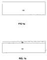
- FIGS. 1 a - 1 frepresent cross-sections of structures that may be formed when carrying out an embodiment of the method of the present invention.
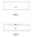
- FIG. 2 a - hrepresent cross-sections of a structure that may be formed when carrying out another embodiment of the method of the present invention.
- FIG. 3is a cross-sectional illustration of a diamond film structure, as is known in the art.
- FIG. 4represents a cross-section of a structure that may be formed when carrying out another embodiment of the present invention.
- Methods of forming a high conductivity diamond film and its associated structurescomprise selectively nucleating diamond on a region of a substrate and then forming a diamond film on the substrate such that the diamond film has large grains, which are about 20 microns in size. Because the thermal conductivity of a diamond film is a function of its grain size, a larger grained diamond film has greatly improved thermal management capabilities, and thus can serve to improve the efficiency and speed of a microelectronic device.
- an abraded (roughened) layer 104is formed on a substrate 102 ( FIG. 1 a - 1 b ).
- the substrate 102may comprise materials such as silicon, silicon-on insulator, germanium, indium antimonide, lead telluride, indium arsenide, indium phosphide, gallium arsenide, or gallium antimonide. Although several examples of materials from which the substrate 102 may be formed are described here, any material that may serve as a foundation upon which a microelectronic device may be built falls within the spirit and scope of the present invention.
- suitable abrasive materials which can be used to abrade the substrate 102 and thus form the abrased layer 104may include silicon carbide particulates as well as diamond particulates. Although a few examples of materials that may be used to abrade the substrate 102 and thus form the abrased layer 104 are described here, the substrate 102 may be abraded with other materials that serve to prepare the substrate 102 for the nucleation (initial stage of diamond film growth wherein individual grains are formed) of a diamond film.
- the abraded layer 104may be formed on the substrate 102 using a variety of methods known in the art, e.g. performing a mechanically abrasive step such as sanding the substrate 102 , or immersing the substrate 102 in an ultrasonic bath which contains a suspension of an abrasive material.
- a dielectric layer 106is deposited onto the abraded layer 104 ( FIG. 1 c ).
- the dielectric layer 106may be formed using a variety of materials, such as silicon nitride or silicon dioxide. Although a few examples of materials that may be used to form the dielectric layer 106 are described here, that layer may be made from other materials that serve to prevent the formation of a diamond film on the substrate 102 .
- the dielectric layer 106may be deposited using conventional techniques such as physical vapor deposition (“PVD”), atomic layer deposition (“ALD”), conventional chemical vapor deposition (“CVD”), low pressure CVD, plasma enhanced CVD or other such methods known to those skilled in the art.
- PVDphysical vapor deposition
- ALDatomic layer deposition
- CVDchemical vapor deposition
- low pressure CVDlow pressure CVD
- plasma enhanced CVDplasma enhanced CVD or other such methods known to those skilled in the art.
- the dielectric layer 106is preferably less than 1 micron thick, but must be thick enough to avoid pinholes in the dielectric layer 106 , which could contribute undesired nucleation sites by exposing the underlying abraded layer 104 through the pinholes in the dielectric layer 106 .
- the dielectric layer 106must also be sufficiently thin so that it does not impede the subsequent growth of the diamond grains following the nucleation phase of a diamond film, since a thinner diamond film is more desired in terms of cost and efficiency.
- a plurality of openings 108are then formed in the dielectric layer 106 ( FIG. 1 d ).
- the openings 108define a plurality of nucleation sites 107 , which are the exposed portions of the underlying abraded layer 104 .
- the openings 108may be formed using conventional lithographic techniques, which are well known to those skilled in the art and consequently will not be fully described herein.
- the openings 108which can be of any geometric shape (such as circular, square, triangular, or any appropriately shaped geometry), are preferably about 1 micron or less in size, (preferably 1 micron) and are spaced less than about 50 percent of the final desired thickness of the diamond film, most preferably about 10 to 20 microns apart.
- the spacing of the openings 108depends on such factors as the desired final thickness and thermal conductivity of the diamond film.
- the spacing between the openings 108determines the ultimate size and uniformity of the individual diamond grains that form after the initial nucleation stage of the diamond film, as the diamond film continues to grow and the individual grains coalesce.
- a plurality of diamond grains 110are formed on the nucleation sites 107 , but do not form on the dielectric layer 106 ( FIG. 1 e ).
- the diamond grains 110may be formed on the nucleation sites 107 utilizing conventional methods suitable for the deposition of diamond films known in the art, such as plasma enhanced chemical vapor deposition (“PECVD”)(preferred).
- PECVDplasma enhanced chemical vapor deposition
- the preferred process pressureis in a range from about 10 to 100 Torr, with 40 to 50 Torr most preferred, a temperature of about 600 to 900 degrees, with 800 to 900 most preferred, and a power between about 10 kW to about 200 kW.
- Methods of plasma generationmay include microwave, RF, DC glow and DC arc-jet.
- Gases such as CH 4 , C 2 H 2 , fullerenes or solid carbon gas precursors mixed with a super saturation of hydrogen at 10 to 200 sccm flow ratemay be used, while the preferred gas mix is CH 4 and H 2 in a ratio of 0.5 to 6% CH 4 and 99.4 to 94% H 2 .
- the diamond grains 110are selectively nucleated, i.e. the nucleation sites 107 are confined to the areas created by the openings 108 in the dielectric layer 106 . Thus, continued growth of the diamond grains 110 results in diamond grains 110 that are much larger and more uniform (see FIG.
- the diamond grains 110 of the present inventioncan range from 10-20 microns, and are preferably larger than 20 microns, which approaches the grain size of a single crystal diamond. Consequently, the thermal conductivity of the larger diamond grains 110 approaches that of single crystal diamond (about 2000 W/m-K), and can range from about 600 to above 2000 W/m-K, with greater than 1000 W/m-k preferred.
- the diamond grains 110continue to grow and coalesce until the desired thickness of the diamond layer 112 is achieved.
- the diamond layer 112may be between about 25 and 200 microns thick, most preferably 100 microns thick. A thinner diamond layer 112 is preferred, since they are less expensive to fabricate and easier to integrate into a microelectronic device.
- the diamond layer 112has a thermal conductivity of about 600 to above 2000 W/m-K, with greater than 1000 W/m-k preferred.
- the present inventionprovides methods and structures formed thereby of forming a thin diamond layer 112 with uniformly large grains that also exhibits high thermal conductivity.
- an abraded layer 204is formed on a substrate 202 ( FIGS. 2 a - 2 b ), as has been previously described herein (see FIGS. 1 a - 1 b ).
- a masking layer 206is deposited onto the abraded layer 204 ( FIG. 2 c ).
- the masking layer 206may be formed from a variety of materials, such as photoresist. Although an example of materials that may be used to form the masking layer 206 are described here, that layer may be made from other materials that serve to prevent the polishing of the substrate 102 .
- the masking layer 206may be deposited using conventional techniques which are well known in the art, and will not be described herein.
- a plurality of masked areas 208are then formed from the masking layer 206 using conventional photolithographic techniques known in the art that will not be described herein ( FIG. 2 d ).
- the masked areas 208which can be of any geometric shape, are preferably about 1 micron or less in size, (preferably 1 micron) and are spaced less than about 50 percent of the final desired thickness of the diamond film, most preferably about 5 to 20 microns apart. It is to be understood that the spacing of the masked areas 208 depends on such factors as the desired final thickness and thermal conductivity of the diamond film.
- the spacing between the masked areas 208determines the ultimate size and uniformity of the individual diamond grains that form after the initial nucleation stage of the diamond film, as the diamond film continues to grow and the individual grains coalesce.
- the abraded layer 204is then etched using conventional techniques known in the art (not described herein) to remove the surface damage (caused from the abrasion of the substrate 202 ) in all areas except those areas protected by the masking areas 208 ( FIG. 2 e ).
- the etching of the abraded layer 204defines a plurality of nucleation sites 207 underneath the masking areas 208 .
- the nucleation sites 207are then exposed after the masking areas 208 are subsequently removed using conventional photolithographic techniques ( FIG. 2 f ).
- a plurality of diamond grains 210are formed on the nucleation sites 207 , but do not form on the substrate 202 ( FIG. 2 g ).
- the diamond grains 210may be deposited using the same methods as the earlier described embodiment of the present invention.
- the diamond grains 210are selectively nucleated, ie. the diamond grains grow only on the nucleation sites 207 .
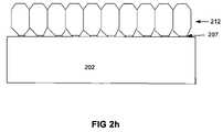
- continued growth of the diamond grains 210results in diamond layer 212 having diamond grains 210 that are much larger and more uniform (see FIG.
- the diamond grains 210 of the present inventioncan range from 10-20 microns, and are preferably larger than 20 microns, which approaches the grain size of a single crystal diamond. Consequently, the thermal conductivity of the larger diamond grains 110 approaches that of single crystal diamond (about 2000 W/m-K).
- the diamond grains 210continue to grow and coalesce until the desired thickness of the diamond layer 212 is achieved ( FIG. 2 h ).
- the diamond layer 212may be between about 25 and 200 microns thick, and is most preferably 100 microns thick.
- the diamond layer 212has a thermal conductivity of about 600 to above 2000 W/m-K, with greater than 1000 W/m-k preferred.
- a diamond layer 312which is formed according to the methods of the present invention, may be attached to a substrate 302 (as previously described herein), wherein the substrate contains a plurality of integrated circuits 304 , which may comprise various circuit elements such as, by way of illustration and not limitation, a plurality of transistors 306 .
- the substrate 302may further be ground or polished to a thickness of about 1 to 3 microns thick.
- the diamond layer 312may be attached by various methods as are known in the art, such as by depositing the diamond layer 312 by PECVD onto the substrate 302 , or by bonding the substrate 302 to the diamond layer 312 .
- the diamond layer 312may serve to provide a mechanism by which thermal hot spots on the integrated circuit 304 are greatly reduced, which in turn increases the speed and reliability of the integrated circuit 304 .
- the present inventionprovides methods and structures formed thereby of selectively nucleating a substrate in order to promote the growth of large grained diamond films which have a high thermal conductivity.
- This increase in the thermal conductivitygreatly improves the ability of a diamond film to thermally manage a microelectronic device, such as in the thermal management of hot spots across a device.
- the reliability and speed of a microelectronic deviceare greatly enhanced.
Landscapes
- Engineering & Computer Science (AREA)
- Computer Hardware Design (AREA)
- Power Engineering (AREA)
- Manufacturing & Machinery (AREA)
- Microelectronics & Electronic Packaging (AREA)
- Condensed Matter Physics & Semiconductors (AREA)
- General Physics & Mathematics (AREA)
- Physics & Mathematics (AREA)
- Chemical & Material Sciences (AREA)
- Materials Engineering (AREA)
- Crystallography & Structural Chemistry (AREA)
- Organic Chemistry (AREA)
- Metallurgy (AREA)
- General Chemical & Material Sciences (AREA)
- Chemical Kinetics & Catalysis (AREA)
- Crystals, And After-Treatments Of Crystals (AREA)
- Recrystallisation Techniques (AREA)
- Cooling Or The Like Of Semiconductors Or Solid State Devices (AREA)
Abstract
Description
Claims (9)
Priority Applications (1)
| Application Number | Priority Date | Filing Date | Title |
|---|---|---|---|
| US10/973,161US7417255B2 (en) | 2002-12-05 | 2004-10-25 | Methods of forming a high conductivity diamond film and structures formed thereby |
Applications Claiming Priority (2)
| Application Number | Priority Date | Filing Date | Title |
|---|---|---|---|
| US10/313,686US7501330B2 (en) | 2002-12-05 | 2002-12-05 | Methods of forming a high conductivity diamond film and structures formed thereby |
| US10/973,161US7417255B2 (en) | 2002-12-05 | 2004-10-25 | Methods of forming a high conductivity diamond film and structures formed thereby |
Related Parent Applications (1)
| Application Number | Title | Priority Date | Filing Date |
|---|---|---|---|
| US10/313,686DivisionUS7501330B2 (en) | 2002-12-05 | 2002-12-05 | Methods of forming a high conductivity diamond film and structures formed thereby |
Publications (2)
| Publication Number | Publication Date |
|---|---|
| US20050112793A1 US20050112793A1 (en) | 2005-05-26 |
| US7417255B2true US7417255B2 (en) | 2008-08-26 |
Family
ID=32468316
Family Applications (3)
| Application Number | Title | Priority Date | Filing Date |
|---|---|---|---|
| US10/313,686Expired - Fee RelatedUS7501330B2 (en) | 2002-12-05 | 2002-12-05 | Methods of forming a high conductivity diamond film and structures formed thereby |
| US10/973,161Expired - LifetimeUS7417255B2 (en) | 2002-12-05 | 2004-10-25 | Methods of forming a high conductivity diamond film and structures formed thereby |
| US11/100,885Expired - Fee RelatedUS7553694B2 (en) | 2002-12-05 | 2005-04-04 | Methods of forming a high conductivity diamond film and structures formed thereby |
Family Applications Before (1)
| Application Number | Title | Priority Date | Filing Date |
|---|---|---|---|
| US10/313,686Expired - Fee RelatedUS7501330B2 (en) | 2002-12-05 | 2002-12-05 | Methods of forming a high conductivity diamond film and structures formed thereby |
Family Applications After (1)
| Application Number | Title | Priority Date | Filing Date |
|---|---|---|---|
| US11/100,885Expired - Fee RelatedUS7553694B2 (en) | 2002-12-05 | 2005-04-04 | Methods of forming a high conductivity diamond film and structures formed thereby |
Country Status (1)
| Country | Link |
|---|---|
| US (3) | US7501330B2 (en) |
Families Citing this family (12)
| Publication number | Priority date | Publication date | Assignee | Title |
|---|---|---|---|---|
| US7132309B2 (en)* | 2003-04-22 | 2006-11-07 | Chien-Min Sung | Semiconductor-on-diamond devices and methods of forming |
| US7501330B2 (en)* | 2002-12-05 | 2009-03-10 | Intel Corporation | Methods of forming a high conductivity diamond film and structures formed thereby |
| US20070232074A1 (en)* | 2006-03-31 | 2007-10-04 | Kramadhati Ravi | Techniques for the synthesis of dense, high-quality diamond films using a dual seeding approach |
| WO2010010176A1 (en)* | 2008-07-25 | 2010-01-28 | Commissariat A L'energie Atomique | Process for microstructuring a diamond film |
| US8889076B2 (en)* | 2008-12-29 | 2014-11-18 | Uop Llc | Fluid catalytic cracking system and process |
| JP5777962B2 (en)* | 2011-07-14 | 2015-09-16 | 日本バイリーン株式会社 | Method for producing diamond film |
| FR3001466B1 (en)* | 2013-01-29 | 2016-05-27 | Commissariat Energie Atomique | METHOD FOR MANUFACTURING MONOCRYSTALLINE DIAMOND ELEMENTS OR WITH LOW DENSITY OF MICRO, SUBMICRO OR NANOMETER-SIZED GRAIN JOINTS |
| US9835778B1 (en) | 2013-09-13 | 2017-12-05 | Lockheed Martin Corporation | Apparatus and method for a diamond substrate for a multi-layered dielectric diffraction grating |
| US9366872B2 (en) | 2014-02-18 | 2016-06-14 | Lockheed Martin Corporation | Apparatus and method for fiber-laser output-beam shaping for spectral beam combination |
| JP6407475B2 (en)* | 2016-03-18 | 2018-10-17 | 三菱電機株式会社 | Semiconductor device and method for producing semiconductor device |
| CN113571409B (en)* | 2021-07-02 | 2022-04-15 | 北京科技大学 | A kind of preparation method of high thermal conductivity diamond reinforced silicon carbide substrate |
| NL2032889B1 (en)* | 2022-08-29 | 2024-03-12 | Univ Delft Tech | Heteroepitaxial growth of single crystalline diamond on a substrate |
Citations (41)
| Publication number | Priority date | Publication date | Assignee | Title |
|---|---|---|---|---|
| US4259090A (en)* | 1979-11-19 | 1981-03-31 | General Electric Company | Method of making diamond compacts for rock drilling |
| US5082522A (en) | 1990-08-14 | 1992-01-21 | Texas Instruments Incorporated | Method for forming patterned diamond thin films |
| US5242711A (en) | 1991-08-16 | 1993-09-07 | Rockwell International Corp. | Nucleation control of diamond films by microlithographic patterning |
| US5298286A (en) | 1992-11-09 | 1994-03-29 | North Carolina State University | Method for fabricating diamond films on nondiamond substrates and related structures |
| US5432003A (en) | 1988-10-03 | 1995-07-11 | Crystallume | Continuous thin diamond film and method for making same |
| US5443032A (en) | 1992-06-08 | 1995-08-22 | Air Products And Chemicals, Inc. | Method for the manufacture of large single crystals |
| US5449531A (en) | 1992-11-09 | 1995-09-12 | North Carolina State University | Method of fabricating oriented diamond films on nondiamond substrates and related structures |
| US5474808A (en) | 1994-01-07 | 1995-12-12 | Michigan State University | Method of seeding diamond |
| US5478513A (en)* | 1991-12-13 | 1995-12-26 | General Electric Company | CVD diamond growth on hydride-forming metal substrates |
| US5488350A (en) | 1994-01-07 | 1996-01-30 | Michigan State University | Diamond film structures and methods related to same |
| US5488232A (en) | 1993-09-28 | 1996-01-30 | North Carolina State University | Oriented diamond film structures on non-diamond substrates |
| US5501877A (en) | 1994-09-19 | 1996-03-26 | University Of Florida | Patterned deposition of thin films |
| US5541423A (en)* | 1991-11-21 | 1996-07-30 | Canon Kabushiki Kaisha | Monocrystalline diamond semiconductor device and several electronic components employing same |
| US5559367A (en) | 1994-07-12 | 1996-09-24 | International Business Machines Corporation | Diamond-like carbon for use in VLSI and ULSI interconnect systems |
| US5607723A (en) | 1988-10-21 | 1997-03-04 | Crystallume | Method for making continuous thin diamond film |
| US5614272A (en)* | 1992-11-19 | 1997-03-25 | E. I. Du Pont De Nemours And Company | Method for making small dimensional diamond-coated graphite articles |
| US5614019A (en)* | 1992-06-08 | 1997-03-25 | Air Products And Chemicals, Inc. | Method for the growth of industrial crystals |
| US5654044A (en)* | 1995-08-29 | 1997-08-05 | The United States Of America As Represented By The Secretary Of The Navy | Diamond film deposition on graphite |
| US5656828A (en) | 1994-05-04 | 1997-08-12 | Daimler-Benz Ag | Electronic component with a semiconductor composite structure |
| US5683939A (en) | 1993-04-02 | 1997-11-04 | Harris Corporation | Diamond insulator devices and method of fabrication |
| US5686152A (en) | 1995-08-03 | 1997-11-11 | Johnson; Linda F. | Metal initiated nucleation of diamond |
| US5733369A (en)* | 1986-03-28 | 1998-03-31 | Canon Kabushiki Kaisha | Method for forming crystal |
| US5750243A (en) | 1994-06-20 | 1998-05-12 | Sumitomo Electric Industries, Ltd. | Surface acoustic wave device and diamond base material for the same |
| US5795653A (en) | 1993-01-19 | 1998-08-18 | International Business Machines Corporation | Method for polishing a diamond or carbon nitride film by reaction with oxygen transported to the film through a superionic conductor in contact with the film |
| US5812362A (en) | 1996-06-14 | 1998-09-22 | Applied Materials, Inc. | Method and apparatus for the use of diamond films as dielectric coatings on electrostatic chucks |
| US5843224A (en) | 1994-08-05 | 1998-12-01 | Daimler-Benz Aktiengesellschaft | Composite structure comprising a semiconductor layer arranged on a diamond or diamond-like layer and process for its production |
| US5855954A (en) | 1995-11-11 | 1999-01-05 | Daimler-Benz Ag | Composite structure for manufacturing a microelectronic component and a process for manufacturing the composite structure |
| US5891575A (en) | 1994-06-28 | 1999-04-06 | United States As Represented By The Secretary Of The Navy | Growing and releasing diamonds |
| US5939140A (en) | 1994-06-13 | 1999-08-17 | Sumitomo Electric Industries, Ltd. | Hot filament CVD of diamond films |
| US6082200A (en) | 1997-09-19 | 2000-07-04 | Board Of Trustees Operating Michigan State University | Electronic device and method of use thereof |
| US6110759A (en) | 1997-05-02 | 2000-08-29 | Daimlerchrysler Ag | Composite structure with a growth substrate having a diamond layer and a plurality of microelectronic components, and process for producing such a composite structure |
| US6126855A (en) | 1987-07-27 | 2000-10-03 | Elliott; Stanley B. | Reaction products of lyotropic liquid crystal salt complexes |
| US6537668B1 (en) | 1996-05-31 | 2003-03-25 | United Module Corporation, Inc. | Recording media having protective overcoats of highly tetrahedral amorphous carbon and methods for their production |
| US20040108506A1 (en)* | 2002-12-05 | 2004-06-10 | Ravi Kramadhati V. | Methods of forming a high conductivity diamond film and structures formed thereby |
| US6770966B2 (en) | 2001-07-31 | 2004-08-03 | Intel Corporation | Electronic assembly including a die having an integrated circuit and a layer of diamond to transfer heat |
| US6783589B2 (en)* | 2001-01-19 | 2004-08-31 | Chevron U.S.A. Inc. | Diamondoid-containing materials in microelectronics |
| US20040191534A1 (en) | 2003-03-27 | 2004-09-30 | Intel Corporation | Stress-reducing structure for electronic devices |
| US20040188262A1 (en) | 2002-02-05 | 2004-09-30 | Heimann Robert L. | Method for treating metallic surfaces and products formed thereby |
| US20050017351A1 (en) | 2003-06-30 | 2005-01-27 | Ravi Kramadhati V. | Silicon on diamond wafers and devices |
| US6936497B2 (en) | 2002-12-24 | 2005-08-30 | Intel Corporation | Method of forming electronic dies wherein each die has a layer of solid diamond |
| US6987028B2 (en) | 2003-07-24 | 2006-01-17 | Intel Corporation | Method of fabricating a microelectronic die |
Family Cites Families (2)
| Publication number | Priority date | Publication date | Assignee | Title |
|---|---|---|---|---|
| JP2743514B2 (en)* | 1989-09-29 | 1998-04-22 | 株式会社島津製作所 | Method for producing polycrystalline diamond thin film |
| US6674098B1 (en)* | 1999-07-26 | 2004-01-06 | National Institute Of Advanced Industrial Science And Technology | ZnO compound semiconductor light emitting element |
- 2002
- 2002-12-05USUS10/313,686patent/US7501330B2/ennot_activeExpired - Fee Related
- 2004
- 2004-10-25USUS10/973,161patent/US7417255B2/ennot_activeExpired - Lifetime
- 2005
- 2005-04-04USUS11/100,885patent/US7553694B2/ennot_activeExpired - Fee Related
Patent Citations (55)
| Publication number | Priority date | Publication date | Assignee | Title |
|---|---|---|---|---|
| US4259090A (en)* | 1979-11-19 | 1981-03-31 | General Electric Company | Method of making diamond compacts for rock drilling |
| US5733369A (en)* | 1986-03-28 | 1998-03-31 | Canon Kabushiki Kaisha | Method for forming crystal |
| US5853478A (en)* | 1986-03-28 | 1998-12-29 | Canon Kabushiki Kaisha | Method for forming crystal and crystal article obtained by said method |
| US6126855A (en) | 1987-07-27 | 2000-10-03 | Elliott; Stanley B. | Reaction products of lyotropic liquid crystal salt complexes |
| US5432003A (en) | 1988-10-03 | 1995-07-11 | Crystallume | Continuous thin diamond film and method for making same |
| US5607723A (en) | 1988-10-21 | 1997-03-04 | Crystallume | Method for making continuous thin diamond film |
| US5082522A (en) | 1990-08-14 | 1992-01-21 | Texas Instruments Incorporated | Method for forming patterned diamond thin films |
| US5242711A (en) | 1991-08-16 | 1993-09-07 | Rockwell International Corp. | Nucleation control of diamond films by microlithographic patterning |
| US5541423A (en)* | 1991-11-21 | 1996-07-30 | Canon Kabushiki Kaisha | Monocrystalline diamond semiconductor device and several electronic components employing same |
| US5478513A (en)* | 1991-12-13 | 1995-12-26 | General Electric Company | CVD diamond growth on hydride-forming metal substrates |
| US5443032A (en) | 1992-06-08 | 1995-08-22 | Air Products And Chemicals, Inc. | Method for the manufacture of large single crystals |
| US5614019A (en)* | 1992-06-08 | 1997-03-25 | Air Products And Chemicals, Inc. | Method for the growth of industrial crystals |
| US5449531A (en) | 1992-11-09 | 1995-09-12 | North Carolina State University | Method of fabricating oriented diamond films on nondiamond substrates and related structures |
| US5487945A (en) | 1992-11-09 | 1996-01-30 | North Carolina State University | Diamond films on nondiamond substrates |
| US5298286A (en) | 1992-11-09 | 1994-03-29 | North Carolina State University | Method for fabricating diamond films on nondiamond substrates and related structures |
| US5849413A (en) | 1992-11-09 | 1998-12-15 | North Carolina State University | Oriented diamond film structures on nondiamond substrates |
| US5614272A (en)* | 1992-11-19 | 1997-03-25 | E. I. Du Pont De Nemours And Company | Method for making small dimensional diamond-coated graphite articles |
| US5795653A (en) | 1993-01-19 | 1998-08-18 | International Business Machines Corporation | Method for polishing a diamond or carbon nitride film by reaction with oxygen transported to the film through a superionic conductor in contact with the film |
| US5683939A (en) | 1993-04-02 | 1997-11-04 | Harris Corporation | Diamond insulator devices and method of fabrication |
| US5488232A (en) | 1993-09-28 | 1996-01-30 | North Carolina State University | Oriented diamond film structures on non-diamond substrates |
| US5474808A (en) | 1994-01-07 | 1995-12-12 | Michigan State University | Method of seeding diamond |
| US5488350A (en) | 1994-01-07 | 1996-01-30 | Michigan State University | Diamond film structures and methods related to same |
| US5656828A (en) | 1994-05-04 | 1997-08-12 | Daimler-Benz Ag | Electronic component with a semiconductor composite structure |
| US5939140A (en) | 1994-06-13 | 1999-08-17 | Sumitomo Electric Industries, Ltd. | Hot filament CVD of diamond films |
| US5750243A (en) | 1994-06-20 | 1998-05-12 | Sumitomo Electric Industries, Ltd. | Surface acoustic wave device and diamond base material for the same |
| US5891575A (en) | 1994-06-28 | 1999-04-06 | United States As Represented By The Secretary Of The Navy | Growing and releasing diamonds |
| US5559367A (en) | 1994-07-12 | 1996-09-24 | International Business Machines Corporation | Diamond-like carbon for use in VLSI and ULSI interconnect systems |
| US5679269A (en) | 1994-07-12 | 1997-10-21 | International Business Machines, Corp. | Diamond-like carbon for use in VLSI and ULSI interconnect systems |
| US5674355A (en) | 1994-07-12 | 1997-10-07 | International Business Machines Corp. | Diamond-like carbon for use in VLSI and ULSI interconnect systems |
| US5843224A (en) | 1994-08-05 | 1998-12-01 | Daimler-Benz Aktiengesellschaft | Composite structure comprising a semiconductor layer arranged on a diamond or diamond-like layer and process for its production |
| US5501877A (en) | 1994-09-19 | 1996-03-26 | University Of Florida | Patterned deposition of thin films |
| US5686152A (en) | 1995-08-03 | 1997-11-11 | Johnson; Linda F. | Metal initiated nucleation of diamond |
| US5654044A (en)* | 1995-08-29 | 1997-08-05 | The United States Of America As Represented By The Secretary Of The Navy | Diamond film deposition on graphite |
| US5855954A (en) | 1995-11-11 | 1999-01-05 | Daimler-Benz Ag | Composite structure for manufacturing a microelectronic component and a process for manufacturing the composite structure |
| US6544627B1 (en) | 1996-05-31 | 2003-04-08 | United Modular Corporation | Method of producing recording media having protective overcoats of highly tetrahedral amorphous carbon |
| US6805891B2 (en) | 1996-05-31 | 2004-10-19 | United Mobile Corporation | Recording media having protective overcoats of highly tetrahedral amorphous carbon and methods for their production |
| US6740384B2 (en) | 1996-05-31 | 2004-05-25 | Vijayen Veerasamy | Recording media having protective overcoats of highly tetrahedral amorphous carbon and methods for their production |
| US6537668B1 (en) | 1996-05-31 | 2003-03-25 | United Module Corporation, Inc. | Recording media having protective overcoats of highly tetrahedral amorphous carbon and methods for their production |
| US5812362A (en) | 1996-06-14 | 1998-09-22 | Applied Materials, Inc. | Method and apparatus for the use of diamond films as dielectric coatings on electrostatic chucks |
| US6329674B1 (en) | 1997-05-02 | 2001-12-11 | Daimlerchrysler Ag | Composite structure with a growth substrate having a diamond layer and a plurality of microelectronic components, and process for producing such a composite structure |
| US6110759A (en) | 1997-05-02 | 2000-08-29 | Daimlerchrysler Ag | Composite structure with a growth substrate having a diamond layer and a plurality of microelectronic components, and process for producing such a composite structure |
| US6082200A (en) | 1997-09-19 | 2000-07-04 | Board Of Trustees Operating Michigan State University | Electronic device and method of use thereof |
| US6783589B2 (en)* | 2001-01-19 | 2004-08-31 | Chevron U.S.A. Inc. | Diamondoid-containing materials in microelectronics |
| US6921706B2 (en) | 2001-07-31 | 2005-07-26 | Intel Corporation | Electronic assembly including a die having an integrated circuit and a layer of diamond to transfer heat |
| US6770966B2 (en) | 2001-07-31 | 2004-08-03 | Intel Corporation | Electronic assembly including a die having an integrated circuit and a layer of diamond to transfer heat |
| US7170098B2 (en) | 2001-07-31 | 2007-01-30 | Intel Corporation | Electronic assembly including a die having an integrated circuit and a layer of diamond to transfer heat |
| US20040188262A1 (en) | 2002-02-05 | 2004-09-30 | Heimann Robert L. | Method for treating metallic surfaces and products formed thereby |
| US20040108506A1 (en)* | 2002-12-05 | 2004-06-10 | Ravi Kramadhati V. | Methods of forming a high conductivity diamond film and structures formed thereby |
| US20050112793A1 (en)* | 2002-12-05 | 2005-05-26 | Ravi Kramadhati V. | Methods of forming a high conductivity diamond film and structures formed thereby |
| US20050189544A1 (en)* | 2002-12-05 | 2005-09-01 | Ravi Kramadhati V. | Methods of forming a high conductivity diamond film and structures formed thereby |
| US6936497B2 (en) | 2002-12-24 | 2005-08-30 | Intel Corporation | Method of forming electronic dies wherein each die has a layer of solid diamond |
| US6830813B2 (en)* | 2003-03-27 | 2004-12-14 | Intel Corporation | Stress-reducing structure for electronic devices |
| US20040191534A1 (en) | 2003-03-27 | 2004-09-30 | Intel Corporation | Stress-reducing structure for electronic devices |
| US20050017351A1 (en) | 2003-06-30 | 2005-01-27 | Ravi Kramadhati V. | Silicon on diamond wafers and devices |
| US6987028B2 (en) | 2003-07-24 | 2006-01-17 | Intel Corporation | Method of fabricating a microelectronic die |
Non-Patent Citations (10)
| Title |
|---|
| Office Action from U.S. Appl. No. 10/313,686, mailed Dec. 27. 2004 7 pgs. |
| Office Action from U.S. Appl. No. 10/313,686, mailed Jan. 29, 2007, 11 pgs. |
| Office Action from U.S. Appl. No. 10/313,686, mailed Jun. 14, 2005, 7 pgs. |
| Office Action from U.S. Appl. No. 10/313,686, mailed Jun. 14, 2006, 4 pgs. |
| Office Action from U.S. Appl. No. 10/313,686, mailed Nov. 29, 2005, 7 pgs. |
| Office Action from U.S. Appl. No. 10/313,686, mailed Nov. 29, 2007, 5 pgs. |
| Office Action from U.S. Appl. No. 10/313,686, mailed Oct. 5. 2006, 8 pgs. |
| Office Action from U.S. Appl. No. 10/313,686, mailed Sep. 19, 2007, 8 pgs. |
| Office Action from U.S. Appl. No. 10/313,686, mailed Sep. 24, 2004, 6 pgs. |
| Office Action from U.S. Appl. No. 11/100,885, mailed Apr. 4, 20088, 8 pgs. |
Also Published As
| Publication number | Publication date |
|---|---|
| US7553694B2 (en) | 2009-06-30 |
| US20040108506A1 (en) | 2004-06-10 |
| US20050189544A1 (en) | 2005-09-01 |
| US7501330B2 (en) | 2009-03-10 |
| US20050112793A1 (en) | 2005-05-26 |
Similar Documents
| Publication | Publication Date | Title |
|---|---|---|
| US7417255B2 (en) | Methods of forming a high conductivity diamond film and structures formed thereby | |
| TWI656575B (en) | Nanocrystalline diamond carbon film for 3D NAND hard mask applications | |
| US20070232074A1 (en) | Techniques for the synthesis of dense, high-quality diamond films using a dual seeding approach | |
| JP3221025B2 (en) | Plasma process equipment | |
| JPH05218000A (en) | Method for flattening of semiconductor device | |
| JPH09509288A (en) | Method for depositing tungsten nitride using silicon-containing source gas | |
| JPH06267846A (en) | Diamond electronic device and its manufacturing method | |
| US6652762B2 (en) | Method for fabricating nano-sized diamond whisker, and nano-sized diamond whisker fabricated thereby | |
| US6605520B2 (en) | Method of forming silicon-germanium film | |
| US11894230B2 (en) | Tribological properties of diamond films | |
| JPH0620958A (en) | Formation of rough silicon surface and its application | |
| US20220319841A1 (en) | Deposition of low-stress carbon-containing layers | |
| JP3744554B2 (en) | Thin film formation method | |
| US6812154B2 (en) | Plasma etching methods | |
| US11495454B2 (en) | Deposition of low-stress boron-containing layers | |
| US7056763B2 (en) | Composite structure for electronic microsystems and method for production of said composite structure | |
| JP3082683B2 (en) | Tungsten CVD film forming method | |
| JP3214060B2 (en) | Liquid phase CVD method and liquid phase CVD apparatus | |
| JPH05267220A (en) | Method of forming sealing layer and metal plug in semiconductor device | |
| US11791155B2 (en) | Diffusion barriers for germanium | |
| JPH06151661A (en) | Diamond heatsink and its manufacture and semiconductor device | |
| JP2024543225A (en) | Gas phase precursor seeding for diamond film deposition. | |
| JP2630288B2 (en) | Method for manufacturing semiconductor device | |
| JP2009059798A (en) | Method for manufacturing diamond electronic device | |
| JPH06187902A (en) | Semiconductor electron emitting element |
Legal Events
| Date | Code | Title | Description |
|---|---|---|---|
| AS | Assignment | Owner name:INTEL CORPORATION, CALIFORNIA Free format text:ASSIGNMENT OF ASSIGNORS INTEREST;ASSIGNORS:RAVI, KRAMADHATI V.;GARNER, MICHAEL C.;REEL/FRAME:015932/0565;SIGNING DATES FROM 20021203 TO 20030123 | |
| STCF | Information on status: patent grant | Free format text:PATENTED CASE | |
| FPAY | Fee payment | Year of fee payment:4 | |
| FPAY | Fee payment | Year of fee payment:8 | |
| AS | Assignment | Owner name:U.S. BANK NATIONAL ASSOCIATION, AS COLLATERAL AGENT, CALIFORNIA Free format text:SECURITY INTEREST;ASSIGNOR:MICRON TECHNOLOGY, INC.;REEL/FRAME:038669/0001 Effective date:20160426 Owner name:U.S. BANK NATIONAL ASSOCIATION, AS COLLATERAL AGEN Free format text:SECURITY INTEREST;ASSIGNOR:MICRON TECHNOLOGY, INC.;REEL/FRAME:038669/0001 Effective date:20160426 | |
| AS | Assignment | Owner name:MORGAN STANLEY SENIOR FUNDING, INC., AS COLLATERAL AGENT, MARYLAND Free format text:PATENT SECURITY AGREEMENT;ASSIGNOR:MICRON TECHNOLOGY, INC.;REEL/FRAME:038954/0001 Effective date:20160426 Owner name:MORGAN STANLEY SENIOR FUNDING, INC., AS COLLATERAL Free format text:PATENT SECURITY AGREEMENT;ASSIGNOR:MICRON TECHNOLOGY, INC.;REEL/FRAME:038954/0001 Effective date:20160426 | |
| AS | Assignment | Owner name:U.S. BANK NATIONAL ASSOCIATION, AS COLLATERAL AGENT, CALIFORNIA Free format text:CORRECTIVE ASSIGNMENT TO CORRECT THE REPLACE ERRONEOUSLY FILED PATENT #7358718 WITH THE CORRECT PATENT #7358178 PREVIOUSLY RECORDED ON REEL 038669 FRAME 0001. ASSIGNOR(S) HEREBY CONFIRMS THE SECURITY INTEREST;ASSIGNOR:MICRON TECHNOLOGY, INC.;REEL/FRAME:043079/0001 Effective date:20160426 Owner name:U.S. BANK NATIONAL ASSOCIATION, AS COLLATERAL AGEN Free format text:CORRECTIVE ASSIGNMENT TO CORRECT THE REPLACE ERRONEOUSLY FILED PATENT #7358718 WITH THE CORRECT PATENT #7358178 PREVIOUSLY RECORDED ON REEL 038669 FRAME 0001. ASSIGNOR(S) HEREBY CONFIRMS THE SECURITY INTEREST;ASSIGNOR:MICRON TECHNOLOGY, INC.;REEL/FRAME:043079/0001 Effective date:20160426 | |
| AS | Assignment | Owner name:JPMORGAN CHASE BANK, N.A., AS COLLATERAL AGENT, ILLINOIS Free format text:SECURITY INTEREST;ASSIGNORS:MICRON TECHNOLOGY, INC.;MICRON SEMICONDUCTOR PRODUCTS, INC.;REEL/FRAME:047540/0001 Effective date:20180703 Owner name:JPMORGAN CHASE BANK, N.A., AS COLLATERAL AGENT, IL Free format text:SECURITY INTEREST;ASSIGNORS:MICRON TECHNOLOGY, INC.;MICRON SEMICONDUCTOR PRODUCTS, INC.;REEL/FRAME:047540/0001 Effective date:20180703 | |
| AS | Assignment | Owner name:MICRON TECHNOLOGY, INC., IDAHO Free format text:RELEASE BY SECURED PARTY;ASSIGNOR:U.S. BANK NATIONAL ASSOCIATION, AS COLLATERAL AGENT;REEL/FRAME:047243/0001 Effective date:20180629 | |
| AS | Assignment | Owner name:MICRON TECHNOLOGY, INC., IDAHO Free format text:RELEASE BY SECURED PARTY;ASSIGNOR:MORGAN STANLEY SENIOR FUNDING, INC., AS COLLATERAL AGENT;REEL/FRAME:050937/0001 Effective date:20190731 | |
| AS | Assignment | Owner name:MICRON TECHNOLOGY, INC., IDAHO Free format text:RELEASE BY SECURED PARTY;ASSIGNOR:JPMORGAN CHASE BANK, N.A., AS COLLATERAL AGENT;REEL/FRAME:051028/0001 Effective date:20190731 Owner name:MICRON SEMICONDUCTOR PRODUCTS, INC., IDAHO Free format text:RELEASE BY SECURED PARTY;ASSIGNOR:JPMORGAN CHASE BANK, N.A., AS COLLATERAL AGENT;REEL/FRAME:051028/0001 Effective date:20190731 | |
| MAFP | Maintenance fee payment | Free format text:PAYMENT OF MAINTENANCE FEE, 12TH YEAR, LARGE ENTITY (ORIGINAL EVENT CODE: M1553); ENTITY STATUS OF PATENT OWNER: LARGE ENTITY Year of fee payment:12 |