US7415369B1 - Calibration of voltage-controlled oscillators - Google Patents
Calibration of voltage-controlled oscillatorsDownload PDFInfo
- Publication number
- US7415369B1 US7415369B1US11/801,185US80118507AUS7415369B1US 7415369 B1US7415369 B1US 7415369B1US 80118507 AUS80118507 AUS 80118507AUS 7415369 B1US7415369 B1US 7415369B1
- Authority
- US
- United States
- Prior art keywords
- voltage
- vco
- bias current
- value
- bias
- Prior art date
- Legal status (The legal status is an assumption and is not a legal conclusion. Google has not performed a legal analysis and makes no representation as to the accuracy of the status listed.)
- Active
Links
- 238000000034methodMethods0.000claimsabstractdescription17
- 238000005070samplingMethods0.000claimsdescription7
- 238000001514detection methodMethods0.000description3
- 238000005516engineering processMethods0.000description3
- 230000010365information processingEffects0.000description3
- 238000012986modificationMethods0.000description3
- 230000004048modificationEffects0.000description3
- 230000003139buffering effectEffects0.000description2
- 239000003990capacitorSubstances0.000description2
- 238000006243chemical reactionMethods0.000description2
- 238000012544monitoring processMethods0.000description2
- 230000003071parasitic effectEffects0.000description2
- 101100113692Caenorhabditis elegans clk-2 geneProteins0.000description1
- 101100003180Colletotrichum lindemuthianum ATG1 geneProteins0.000description1
- 230000004075alterationEffects0.000description1
- 238000013459approachMethods0.000description1
- 230000007423decreaseEffects0.000description1
- 238000002955isolationMethods0.000description1
- 229910044991metal oxideInorganic materials0.000description1
- 150000004706metal oxidesChemical class0.000description1
- 238000012545processingMethods0.000description1
- 239000004065semiconductorSubstances0.000description1
Images


Classifications
- H—ELECTRICITY
- H03—ELECTRONIC CIRCUITRY
- H03L—AUTOMATIC CONTROL, STARTING, SYNCHRONISATION OR STABILISATION OF GENERATORS OF ELECTRONIC OSCILLATIONS OR PULSES
- H03L7/00—Automatic control of frequency or phase; Synchronisation
- H03L7/06—Automatic control of frequency or phase; Synchronisation using a reference signal applied to a frequency- or phase-locked loop
- H03L7/08—Details of the phase-locked loop
- H03L7/099—Details of the phase-locked loop concerning mainly the controlled oscillator of the loop
Definitions
- the inventionrelates generally to the calibration of voltage-controlled oscillators (VCOs), and more specifically to the calibration of VCOs to minimize phase noise.
- VCOsvoltage-controlled oscillators
- VCOsare important circuit elements for a wide range of applications, including function generators, phase-locked loops and frequency synthesizers. VCOs produce an oscillating output with a frequency that is controlled by an applied DC voltage.
- phase noiseOne of the challenges associated with VCOs is phase noise. It is well known that bias transistors are a significant contributor of 1/f 3 phase noise for complimentary metal-oxide semiconductor (CMOS) VCOs. It is also known that an optimum bias current exists for each VCO to minimize the 1/f 3 phase noise. However, due to variations in the operating frequency, voltage, temperature and processing of a VCO, it is quite difficult to identify this optimum bias current.
- CMOScomplimentary metal-oxide semiconductor
- a voltage-controlled oscillatorincludes (a) means for altering a bias current of the voltage-controlled oscillator and for monitoring an average voltage at a common-mode node of the voltage-controlled oscillator; (b) means for identifying an optimum bias current corresponding to an extreme value of the average voltage; and (c) means for calibrating the voltage-controlled oscillator using the optimum bias current to minimize 1/f 3 phase noise.
- an information-processing systemin another aspect of the invention, includes a voltage-controlled oscillator.
- the voltage-controlled oscillatorincludes a calibration circuit for altering a bias current of the voltage-controlled oscillator and for monitoring an average voltage at a common-mode node of the voltage-controlled oscillator.
- the calibration circuitidentifies an optimum bias current corresponding to an extreme value of the average voltage and calibrates the voltage-controlled oscillator using the optimum bias current to minimize 1/f 3 phase noise.
- a methodfor calibrating a bias current of a voltage-controlled oscillator to minimize 1/f 3 phase noise.
- the methodcomprises the steps of (a) setting the bias current to a first predetermined value; (b) sampling an average value, corresponding to the bias current, of a common-mode voltage of the voltage-controlled oscillator; (c) varying the bias current by a predetermined amount towards a second predetermined value; (d) repeating the sampling and varying until an optimum bias current corresponding to an extreme value of said average value of the common-mode voltage is identified; and (e) calibrating the voltage-controlled oscillator using the optimum bias current.
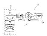
- FIG. 1illustrates a prior art CMOS LC VCO that is suitable for use with the present invention.
- FIG. 2illustrates an exemplary embodiment of a calibration circuit for calibrating the VCO of FIG. 1 to minimize phase noise.
- FIG. 3is a graph that illustrates an exemplary relationship between the bias current and the average voltage at the common-mode node of a VCO.
- FIG. 4illustrates a second example of a prior art CMOS LC VCO that is suitable for use with the present invention.
- FIG. 5illustrates a second exemplary embodiment of a calibration circuit for calibrating the VCO of FIG. 1 to minimize 1/f 3 phase noise.
- FIG. 6is a flowchart that illustrates exemplary steps for a method that is consistent with the present invention.
- FIG. 1illustrates an example of a prior art VCO 10 that is suitable for use with methods and systems of the present invention.
- the VCO 10 illustrated in FIG. 1is a differential CMOS inductor-capacitor (LC) VCO.
- the VCO 10generates differential outputs (V osc0 and V osc1 ), which are 180 degrees out of phase.
- the frequency of V osc0 and V osc1is determined by an applied voltage (V tune ) and by the values of an inductor (L) and two varacters (C 1 and C 2 ), along with parasitic capacitance.
- the VCO 10is biased by a biasing transistor (M bias ).
- the amount of bias current (I bias ) that passes through the biasing transistoris determined by the size of the transistor and a biasing voltage (V bias ).
- the VCO 10also includes two sets of cross-coupled switching transistors (MP 1 , MP 2 and MN 1 , MN 2 ).
- FIG. 2illustrates the VCO 10 of FIG. 1 in combination with an exemplary embodiment of a calibration circuit 20 that is consistent with the present invention.
- the calibration circuit 20includes hardware and/or software for altering the I bias of the VCO 10 and for sampling the associated average voltages at the common-mode node of the VCO.
- the calibration circuitalso includes hardware and/or software for determining the minimum or maximum of the average voltages in order to identify the optimum bias current.
- the input of the calibration circuit 20is connected to the common-mode node of the VCO 10 .
- the output of the calibration circuit 20is connected to modify I bias of the VCO 10 .
- the calibration circuit 20steps the VCO 10 through a range of bias currents by supplying the VCO 10 with a range of I bias values. For each bias current, the calibration circuit 20 determines the corresponding DC value (V cmave ) of the voltage at the common-mode node (V cm ) of the VCO.
- the calibration circuit 20may include a filter 21 to generate V cmave from the common-mode voltage.
- the output of the filter 21may also be connected to a buffer circuit 22 for temporarily buffering the value of V cmave and providing isolation between the VCO and the calibration circuits.
- the buffer circuit 22may be enabled, for example, by an enabling signal (EN).
- ENenabling signal
- the output of the buffer circuit 22is connected to two or more sample-and-hold circuits 24 for sampling and holding a series of V cmave values.
- the output of the sample-and-hold circuits 24are connected to a comparator 26 , which compares the levels of sample values of V cmave .
- the output of the comparator 26is connected to a calibration-logic circuit 28 .
- the calibration-logic circuit 28generates clock signals (clk 0 , clk 1 and clk 2 ) to control the sample-and-hold circuits 24 and the comparator 26 .
- the calibration-logic circuit 28causes the calibration circuit 20 to step the VCO 10 through a range of bias currents while determining the V cmave corresponding to each bias current. The calibration-logic circuit 28 then determines the optimum bias current for the VCO 10 by identifying the bias current that corresponds to the minimum value of V cmave . As an alternative to stepping through an entire range of bias currents, the calibration-logic circuit 28 may identify the minimum value of V cmave by identifying the value at which the slope of V cmave as a function of I bias reverses (see FIG. 3 ).
- FIG. 3illustrates an exemplary relationship between I bias and V cmave for a VCO that is consistent with the present invention.
- the curve in FIG. 3represents V cmave as a function of I bias .
- the point V 1 on the curvecorresponds to a value of V cmave at an I bias value of I1.
- I bias valueAs illustrated by the points V 1 , V 2 and V 3 , there exists a particular value of I bias that corresponds to a minimum value of V cmave . So, for example, when I bias is increased from I1 to I2, V cmave decreases from V 1 to V 2 . When I bias is further increased from I2 to I3, V cmave increases from V 2 to V 3 .
- I biasis further increased from I2 to I3
- V cmaveincreases from V 2 to V 3 .
- the inventor of the present inventionhas determined that the minimum up-conversion of the 1/f device noise from the bias transistor occurs when the switching transistors MN 1 , MN 2 , MP 1 and MP 2 of the VCO are operating at the boundary of their saturation and triode regions. At this boundary, the amplitude of the VCO output is sufficiently large to be symmetrical. Any further increase of amplitude pushes the switching transistors into the triode regions where the up-conversion of the 1/f device noise increases, which leads to a large 1/f 3 phase noise.
- the boundary of the saturation and triode regionscorresponds to the minimum of the average voltage at the common-mode node of the VCO. In other words, a correlation exists between the minimum or maximum value of V cmave and the optimum bias current for minimizing 1/f 3 phase noise.
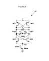
- FIG. 4illustrates a second example of a VCO 40 that is suitable for use with the present invention.
- This VCO 40is a CMOS LC VCO with an NMOS biasing transistor.
- this VCO 40generates differential outputs (V osc0 and V osc1 ), which are 180 degrees out of phase.
- the oscillating frequency of the outputsis determined by the applied voltage (V tune ) and by the values of the inductor (L) and the varacters (C 1 and C 2 ), along with parasitic capacitance.
- the VCO 40is biased by a biasing transistor (M bias ).
- the amount of bias current that passes through the biasing transistoris determined by the size of the transistor and bias voltage (V bias ).
- the VCO 40includes two sets of cross-coupled transistors (MP 1 , MP 2 and MN 1 , MN 2 ). For this VCO 40 , the optimum bias current corresponds to the maximum value of the average voltage at the common-mode node (V cmave ). Identifying the maximum value of V cmave enables the VCO to be calibrated to minimize phase noise.
- VCOs described above with reference to FIGS. 1 and 4are only two examples of VCO configurations that are suitable for use with the present invention.
- VCOs with different arrangements of inductors, capacitors and varactors and VCOs with different types of transistors, such as NMOS and PMOS transistorsare only two examples of VCO configurations that are suitable for use with the present invention.
- VCOs with different arrangements of inductors, capacitors and varactorsare suitable for use with methods and systems of the present invention, including VCOs with different arrangements of inductors, capacitors and varactors and VCOs with different types of transistors, such as NMOS and PMOS transistors.
- FIG. 5illustrates a second embodiment of a calibration circuit 50 that is consistent with the present invention.
- the calibration circuit 50is connected to a VCO 10 , which was previously illustrated in FIG. 1 .
- the input of the calibration circuit 50is connected to the common-mode node of the VCO 10 .
- the output of the calibration circuit 50is connected to the V bias node of the VCO 10 .
- the calibration circuit 50steps the VCO 10 through a range of bias currents by supplying the VCO 10 with a range of V bias values. For each amplitude of the bias current, the calibration circuit 50 determines the corresponding value of V cmave .
- the calibration circuit 50may include a filter 51 for generating V cmave from the common-mode voltage (V cm ).
- the output of the filter 51may be connected to a buffer circuit 52 for temporarily buffering the value of V cmave .
- the buffer circuit 52may be enabled, for example, by an enabling signal (EN).
- ENenabling signal
- the output of the buffer circuit 52is connected to a sample-and-hold circuit 54 for sampling and holding values of V cmave .
- the output of the sample-and-hold circuit 54is connected to an analog-to-digital converter 56 , which converts the analog samples of V cmave into digital signals.
- the output of the analog-to-digital converter 56is connected to a calibration-logic circuit 58 .
- the calibration-logic circuit 58generates a clock signal (clk 0 ) for controlling the sample-and-hold circuit 54 .
- the calibration-logic circuit 58causes the calibration circuit 50 to vary the VCO 10 through a range of bias currents and determines the corresponding V cmave .
- the calibration-logic circuit 58identifies the bias current that corresponds to the minimum V cmave so that it may be used to calibrate the VCO 10 .
- FIG. 6is a flowchart illustrating steps associated with an exemplary method 60 that is consistent with the present invention.
- I biasis set to a first predetermined level. This predetermined level may be, for example, the maximum or minimum bias current associated with the VCO being calibrated.
- V na first voltage level at the common-node of the VCO and its corresponding DC value (V cmave ) are sampled for the first I bias .
- I biasis varied by a predetermined amount, for example by increasing I bias stepwise, toward a second predetermined level. The amount by which I bias is varied and the range over which I bias is varied may be changed depending on the desired speed and accuracy of the calibration.
- the first predetermined levelmay be, for example, the minimum I bias for the VCO and the second predetermined level may be, for example, the maximum I bias for the VCO. In this way, the full range of I bias amplitudes associated with the VCO may be evaluated by the calibration circuit.
- step 64a second voltage level (V n+1 ) at the common-node of the VCO and its corresponding DC value (V cmave ) are sampled for the new I bias .
- step 65the value of V cmave for the first and second voltage levels (V n and V n+1 ) are compared.
- step 66if V cmave for V n+1 is greater than V cmave for V n , the process proceeds to step 69 in which the I bias for the VCO is calibrated using the value corresponding to V n . If V cmave for V n+1 is not greater than V cmave for V n , the process proceeds to step 68 .
- step 68value of n is increased by one and the process returns to step 63 .
Landscapes
- Inductance-Capacitance Distribution Constants And Capacitance-Resistance Oscillators (AREA)
Abstract
Description
Claims (5)
Priority Applications (3)
| Application Number | Priority Date | Filing Date | Title |
|---|---|---|---|
| US11/801,185US7415369B1 (en) | 2007-05-08 | 2007-05-08 | Calibration of voltage-controlled oscillators |
| US12/171,281US7603244B2 (en) | 2007-05-08 | 2008-07-10 | Calibration of voltage controlled oscillators |
| US12/171,277US7728679B2 (en) | 2007-05-08 | 2008-07-10 | Calibration of voltage controlled oscillators |
Applications Claiming Priority (1)
| Application Number | Priority Date | Filing Date | Title |
|---|---|---|---|
| US11/801,185US7415369B1 (en) | 2007-05-08 | 2007-05-08 | Calibration of voltage-controlled oscillators |
Related Child Applications (2)
| Application Number | Title | Priority Date | Filing Date |
|---|---|---|---|
| US12/171,277DivisionUS7728679B2 (en) | 2007-05-08 | 2008-07-10 | Calibration of voltage controlled oscillators |
| US12/171,281DivisionUS7603244B2 (en) | 2007-05-08 | 2008-07-10 | Calibration of voltage controlled oscillators |
Publications (1)
| Publication Number | Publication Date |
|---|---|
| US7415369B1true US7415369B1 (en) | 2008-08-19 |
Family
ID=39687329
Family Applications (3)
| Application Number | Title | Priority Date | Filing Date |
|---|---|---|---|
| US11/801,185ActiveUS7415369B1 (en) | 2007-05-08 | 2007-05-08 | Calibration of voltage-controlled oscillators |
| US12/171,277Active2027-09-17US7728679B2 (en) | 2007-05-08 | 2008-07-10 | Calibration of voltage controlled oscillators |
| US12/171,281ActiveUS7603244B2 (en) | 2007-05-08 | 2008-07-10 | Calibration of voltage controlled oscillators |
Family Applications After (2)
| Application Number | Title | Priority Date | Filing Date |
|---|---|---|---|
| US12/171,277Active2027-09-17US7728679B2 (en) | 2007-05-08 | 2008-07-10 | Calibration of voltage controlled oscillators |
| US12/171,281ActiveUS7603244B2 (en) | 2007-05-08 | 2008-07-10 | Calibration of voltage controlled oscillators |
Country Status (1)
| Country | Link |
|---|---|
| US (3) | US7415369B1 (en) |
Cited By (3)
| Publication number | Priority date | Publication date | Assignee | Title |
|---|---|---|---|---|
| US20080238559A1 (en)* | 2007-03-28 | 2008-10-02 | Nec Electronics Corporation | Voltage controlled oscillator |
| CN102636216A (en)* | 2012-04-28 | 2012-08-15 | 无锡永阳电子科技有限公司 | Sensor signal calibration device |
| US11152890B2 (en)* | 2020-02-25 | 2021-10-19 | International Business Machines Corporation | Low power oscillator with digital amplitude control |
Families Citing this family (9)
| Publication number | Priority date | Publication date | Assignee | Title |
|---|---|---|---|---|
| US20110053537A1 (en)* | 2009-08-31 | 2011-03-03 | Krishnasawamy Nagaraj | Frequency modulation receiver with a low power frequency synthesizer |
| US8299777B2 (en)* | 2009-12-30 | 2012-10-30 | Echostar Technologies L.L.C. | Calculating a parasitic capacitance of an oscillator circuit |
| US8134417B2 (en) | 2010-06-10 | 2012-03-13 | Advanced Micro Devices, Inc. | Automatic amplitude control for voltage controlled oscillator |
| US9099956B2 (en) | 2011-04-26 | 2015-08-04 | King Abdulaziz City For Science And Technology | Injection locking based power amplifier |
| US9255963B2 (en) | 2011-05-09 | 2016-02-09 | Taiwan Semiconductor Manufacturing Company, Ltd. | Built-in self-test circuit for voltage controlled oscillator |
| US8729968B2 (en)* | 2011-05-09 | 2014-05-20 | Taiwan Semiconductor Manufacturing Company, Ltd. | Built-in self-test circuit for voltage controlled oscillators |
| TWI492519B (en)* | 2012-04-26 | 2015-07-11 | Novatek Microelectronics Corp | Circuit of inductance/capacitance (lc) voltage-controlled oscillator |
| CN104820151B (en)* | 2015-05-08 | 2017-11-14 | 天津百利机械装备集团有限公司中央研究院 | A kind of signal calibrating method of 100A total digitalizations Active Power Filter-APF |
| WO2025154390A1 (en)* | 2024-01-19 | 2025-07-24 | ソニーセミコンダクタソリューションズ株式会社 | Oscillation device |
Citations (3)
| Publication number | Priority date | Publication date | Assignee | Title |
|---|---|---|---|---|
| US5175884A (en) | 1990-06-01 | 1992-12-29 | Motorola, Inc. | Voltage controlled oscillator with current control |
| US5907263A (en) | 1997-11-14 | 1999-05-25 | Cirrus Logic, Inc. | Bias current calibration of voltage controlled oscillator |
| US20050030108A1 (en)* | 1998-11-12 | 2005-02-10 | Broadcom Corporation | Integrated VCO having an improved tuning range over process and temperature variations |
Family Cites Families (3)
| Publication number | Priority date | Publication date | Assignee | Title |
|---|---|---|---|---|
| US7525392B2 (en)* | 2006-08-05 | 2009-04-28 | Tang System | XtalClkChip: trimming-free crystal-free precision reference clock oscillator IC chip |
| JP2005064658A (en)* | 2003-08-08 | 2005-03-10 | Mitsubishi Electric Corp | Over output voltage protection circuit for power amplifier |
| US8093958B2 (en)* | 2007-12-05 | 2012-01-10 | Integrated Device Technology, Inc. | Clock, frequency reference, and other reference signal generator with a controlled quality factor |
- 2007
- 2007-05-08USUS11/801,185patent/US7415369B1/enactiveActive
- 2008
- 2008-07-10USUS12/171,277patent/US7728679B2/enactiveActive
- 2008-07-10USUS12/171,281patent/US7603244B2/enactiveActive
Patent Citations (3)
| Publication number | Priority date | Publication date | Assignee | Title |
|---|---|---|---|---|
| US5175884A (en) | 1990-06-01 | 1992-12-29 | Motorola, Inc. | Voltage controlled oscillator with current control |
| US5907263A (en) | 1997-11-14 | 1999-05-25 | Cirrus Logic, Inc. | Bias current calibration of voltage controlled oscillator |
| US20050030108A1 (en)* | 1998-11-12 | 2005-02-10 | Broadcom Corporation | Integrated VCO having an improved tuning range over process and temperature variations |
Non-Patent Citations (6)
| Title |
|---|
| "A 1.8-GHz LC VCO With 1.3-GHz Tuning Range and Digital Amplitude Calibration," Axel D. Berny, Student Member, IEEE, Ali M. Niknejad, Member, IEEE, and Robert G. Meyer, Fellow, IEEE, IEEE Journal of Solid-State Curcuits, vol. 40, No. 4, Apr. 2005, pp. 909-917. |
| "A 2-V 2.5-GHz-104-dBc/Hz at 100kHz Fully Integrated VCO With Wide-Bade Low-Noise Automatic Amplitude Control Loop,", Alfio Zanchi, Student Member, IEEE, Carlo Samori, Member, IEEE, Salvatore Levantino, Student Member, IEEE, and Andrea L. Lacaita, Senior Member, IEEE, IEEE Journal of Solid-State Circuits, Vole 36, No. 4, Apr. 2001, pp. 611-619. |
| "A Low-Noise, Low-Power VCO With Automatic Amplitude Control for Wireless Applications," Mihai A. Margarit, Joo Leong (Julian) Tham, Member, IEEE Robert G. Meyer, Fellow, IEEE, and M. Jamal Deen, Senior Member, IEEE, IEEE Journal of Solid-State Circuits, Vole 34, No. 6, Jun. 1999, pp. 761-771. |
| "A Study of Digital and Analog Automatic-Amplitude Control Circuitry for Voltage-Controlled Oscillators," John W. M. Rogers, Member, IEEE, David Rahn, and Calvin Plett, Member, IEEE, IEEE Journal of Solid-State Circuits, vol. 38, No. 2, Feb. 2003, pp. 352-356. |
| ISSCC 2002 Session 17/ Advanced RF Techniques / 17.4, "Adaptive Biasing of a 5.8Ghz CMOS Oscillator," Donald A. Hitko, Charles G. Sodini, MIT Microsystems Technology Laboratories, Cambridge, MA, pp. 230-231, ISSCC 2002 Visuals Supplement / (C) IEEE. |
| ISSCC 2002 Session 17/ Advanced RF Techniques / 17.4, "Adaptive Biasing of a 5.8Ghz CMOS Oscillator," Donald A. Hitko, Charles G. Sodini, MIT Microsystems Technology Laboratories, Cambridge, MA, pp. 3 pages total, ISSCC 2002 Visuals Supplement / (C) IEEE. |
Cited By (4)
| Publication number | Priority date | Publication date | Assignee | Title |
|---|---|---|---|---|
| US20080238559A1 (en)* | 2007-03-28 | 2008-10-02 | Nec Electronics Corporation | Voltage controlled oscillator |
| US7911284B2 (en)* | 2007-03-28 | 2011-03-22 | Renesas Electronics Corporation | Voltage controlled oscillator |
| CN102636216A (en)* | 2012-04-28 | 2012-08-15 | 无锡永阳电子科技有限公司 | Sensor signal calibration device |
| US11152890B2 (en)* | 2020-02-25 | 2021-10-19 | International Business Machines Corporation | Low power oscillator with digital amplitude control |
Also Published As
| Publication number | Publication date |
|---|---|
| US20080278247A1 (en) | 2008-11-13 |
| US20080278252A1 (en) | 2008-11-13 |
| US7728679B2 (en) | 2010-06-01 |
| US7603244B2 (en) | 2009-10-13 |
Similar Documents
| Publication | Publication Date | Title |
|---|---|---|
| US7415369B1 (en) | Calibration of voltage-controlled oscillators | |
| US7884655B2 (en) | Control circuitry | |
| US8515374B2 (en) | PLL circuit, and radio communication apparatus equipped with same | |
| EP3269040B1 (en) | Phase locked loop (pll) architecture | |
| JP4089938B2 (en) | Voltage controlled oscillator | |
| JP7521885B2 (en) | Digitally Controlled Oscillators Including Current Mirrors | |
| US9660578B2 (en) | Electronic device with capacitor bank linearization and a linearization method | |
| JP2004320721A (en) | Oscillation circuit and method for controlling the oscillation circuit | |
| CN106656122B (en) | Device and method for adjusting the duty ratio in clock signal | |
| US8710930B2 (en) | Differential ring oscillator and method for calibrating the differential ring oscillator | |
| US7965118B2 (en) | Method and apparatus for achieving 50% duty cycle on the output VCO of a phased locked loop | |
| US9509319B1 (en) | Clock and data recovery circuit | |
| US20080238505A1 (en) | System and method for an automatic coarse tuning of a voltage controlled oscillator in a phase-locked loop (PLL) | |
| CN103580685A (en) | Control circuit and apparatus for digitally controlled oscillator | |
| US20070146082A1 (en) | Frequency synthesizer, wireless communications device, and control method | |
| KR101208565B1 (en) | Voltage controlled oscillator capable of reducing phase noise and jitter with high startup gain and method thereof | |
| US9281826B2 (en) | Circuit, voltage control oscillator, and oscillation frequency control system | |
| US10630301B1 (en) | Temperature-dependent phase-locked loop (PLL) reset for clock synthesizers | |
| JP5053413B2 (en) | Synchronous circuit | |
| US20140191810A1 (en) | Systems and methods for synthesizer locking using iterative numerical techniques | |
| US8248123B2 (en) | Loop filter | |
| US20160254816A1 (en) | Voltage controlled oscillator | |
| KR101419834B1 (en) | Frequency synthesizer using voltage controlled oscillator | |
| US10523154B2 (en) | Oscillator including varactor circuit and method of operation thereof | |
| US7969219B2 (en) | Wide range delay cell |
Legal Events
| Date | Code | Title | Description |
|---|---|---|---|
| AS | Assignment | Owner name:ZEROG WIRELESS, INC., CALIFORNIA Free format text:ASSIGNMENT OF ASSIGNORS INTEREST;ASSIGNORS:WANG, STANLEY;KLEVELAND, BENDIK;LEE, THOMAS H.;REEL/FRAME:019330/0878 Effective date:20070508 | |
| AS | Assignment | Owner name:SILICON VALLEY BANK, CALIFORNIA Free format text:SECURITY AGREEMENT;ASSIGNOR:ZEROG WIRELESS, INC.;REEL/FRAME:020656/0110 Effective date:20080314 | |
| STCF | Information on status: patent grant | Free format text:PATENTED CASE | |
| AS | Assignment | Owner name:AZ1 ACQUISITION CORPORATION,ARIZONA Free format text:MERGER;ASSIGNOR:ZEROG WIRELESS, INC.;REEL/FRAME:024432/0648 Effective date:20100108 Owner name:MICROCHIP TECHNOLOGY INCORPORATED,ARIZONA Free format text:ASSIGNMENT OF ASSIGNORS INTEREST;ASSIGNOR:AZ1 ACQUISITION CORPORATION;REEL/FRAME:024432/0659 Effective date:20100512 Owner name:AZ1 ACQUISITION CORPORATION, ARIZONA Free format text:MERGER;ASSIGNOR:ZEROG WIRELESS, INC.;REEL/FRAME:024432/0648 Effective date:20100108 Owner name:MICROCHIP TECHNOLOGY INCORPORATED, ARIZONA Free format text:ASSIGNMENT OF ASSIGNORS INTEREST;ASSIGNOR:AZ1 ACQUISITION CORPORATION;REEL/FRAME:024432/0659 Effective date:20100512 | |
| FPAY | Fee payment | Year of fee payment:4 | |
| FPAY | Fee payment | Year of fee payment:8 | |
| AS | Assignment | Owner name:JPMORGAN CHASE BANK, N.A., AS ADMINISTRATIVE AGENT, ILLINOIS Free format text:SECURITY INTEREST;ASSIGNOR:MICROCHIP TECHNOLOGY INCORPORATED;REEL/FRAME:041675/0617 Effective date:20170208 Owner name:JPMORGAN CHASE BANK, N.A., AS ADMINISTRATIVE AGENT Free format text:SECURITY INTEREST;ASSIGNOR:MICROCHIP TECHNOLOGY INCORPORATED;REEL/FRAME:041675/0617 Effective date:20170208 | |
| AS | Assignment | Owner name:JPMORGAN CHASE BANK, N.A., AS ADMINISTRATIVE AGENT, ILLINOIS Free format text:SECURITY INTEREST;ASSIGNORS:MICROCHIP TECHNOLOGY INCORPORATED;SILICON STORAGE TECHNOLOGY, INC.;ATMEL CORPORATION;AND OTHERS;REEL/FRAME:046426/0001 Effective date:20180529 Owner name:JPMORGAN CHASE BANK, N.A., AS ADMINISTRATIVE AGENT Free format text:SECURITY INTEREST;ASSIGNORS:MICROCHIP TECHNOLOGY INCORPORATED;SILICON STORAGE TECHNOLOGY, INC.;ATMEL CORPORATION;AND OTHERS;REEL/FRAME:046426/0001 Effective date:20180529 | |
| AS | Assignment | Owner name:WELLS FARGO BANK, NATIONAL ASSOCIATION, AS NOTES COLLATERAL AGENT, CALIFORNIA Free format text:SECURITY INTEREST;ASSIGNORS:MICROCHIP TECHNOLOGY INCORPORATED;SILICON STORAGE TECHNOLOGY, INC.;ATMEL CORPORATION;AND OTHERS;REEL/FRAME:047103/0206 Effective date:20180914 Owner name:WELLS FARGO BANK, NATIONAL ASSOCIATION, AS NOTES C Free format text:SECURITY INTEREST;ASSIGNORS:MICROCHIP TECHNOLOGY INCORPORATED;SILICON STORAGE TECHNOLOGY, INC.;ATMEL CORPORATION;AND OTHERS;REEL/FRAME:047103/0206 Effective date:20180914 | |
| MAFP | Maintenance fee payment | Free format text:PAYMENT OF MAINTENANCE FEE, 12TH YR, SMALL ENTITY (ORIGINAL EVENT CODE: M2553); ENTITY STATUS OF PATENT OWNER: SMALL ENTITY Year of fee payment:12 | |
| AS | Assignment | Owner name:JPMORGAN CHASE BANK, N.A., AS ADMINISTRATIVE AGENT, DELAWARE Free format text:SECURITY INTEREST;ASSIGNORS:MICROCHIP TECHNOLOGY INC.;SILICON STORAGE TECHNOLOGY, INC.;ATMEL CORPORATION;AND OTHERS;REEL/FRAME:053311/0305 Effective date:20200327 | |
| AS | Assignment | Owner name:ATMEL CORPORATION, ARIZONA Free format text:RELEASE BY SECURED PARTY;ASSIGNOR:JPMORGAN CHASE BANK, N.A, AS ADMINISTRATIVE AGENT;REEL/FRAME:053466/0011 Effective date:20200529 Owner name:MICROSEMI STORAGE SOLUTIONS, INC., ARIZONA Free format text:RELEASE BY SECURED PARTY;ASSIGNOR:JPMORGAN CHASE BANK, N.A, AS ADMINISTRATIVE AGENT;REEL/FRAME:053466/0011 Effective date:20200529 Owner name:MICROCHIP TECHNOLOGY INC., ARIZONA Free format text:RELEASE BY SECURED PARTY;ASSIGNOR:JPMORGAN CHASE BANK, N.A, AS ADMINISTRATIVE AGENT;REEL/FRAME:053466/0011 Effective date:20200529 Owner name:MICROSEMI CORPORATION, CALIFORNIA Free format text:RELEASE BY SECURED PARTY;ASSIGNOR:JPMORGAN CHASE BANK, N.A, AS ADMINISTRATIVE AGENT;REEL/FRAME:053466/0011 Effective date:20200529 Owner name:SILICON STORAGE TECHNOLOGY, INC., ARIZONA Free format text:RELEASE BY SECURED PARTY;ASSIGNOR:JPMORGAN CHASE BANK, N.A, AS ADMINISTRATIVE AGENT;REEL/FRAME:053466/0011 Effective date:20200529 | |
| AS | Assignment | Owner name:WELLS FARGO BANK, NATIONAL ASSOCIATION, MINNESOTA Free format text:SECURITY INTEREST;ASSIGNORS:MICROCHIP TECHNOLOGY INC.;SILICON STORAGE TECHNOLOGY, INC.;ATMEL CORPORATION;AND OTHERS;REEL/FRAME:053468/0705 Effective date:20200529 | |
| AS | Assignment | Owner name:WELLS FARGO BANK, NATIONAL ASSOCIATION, AS COLLATERAL AGENT, MINNESOTA Free format text:SECURITY INTEREST;ASSIGNORS:MICROCHIP TECHNOLOGY INCORPORATED;SILICON STORAGE TECHNOLOGY, INC.;ATMEL CORPORATION;AND OTHERS;REEL/FRAME:055671/0612 Effective date:20201217 | |
| AS | Assignment | Owner name:WELLS FARGO BANK, NATIONAL ASSOCIATION, AS NOTES COLLATERAL AGENT, MINNESOTA Free format text:SECURITY INTEREST;ASSIGNORS:MICROCHIP TECHNOLOGY INCORPORATED;SILICON STORAGE TECHNOLOGY, INC.;ATMEL CORPORATION;AND OTHERS;REEL/FRAME:057935/0474 Effective date:20210528 | |
| AS | Assignment | Owner name:MICROSEMI STORAGE SOLUTIONS, INC., ARIZONA Free format text:RELEASE BY SECURED PARTY;ASSIGNOR:JPMORGAN CHASE BANK, N.A., AS ADMINISTRATIVE AGENT;REEL/FRAME:059333/0222 Effective date:20220218 Owner name:MICROSEMI CORPORATION, ARIZONA Free format text:RELEASE BY SECURED PARTY;ASSIGNOR:JPMORGAN CHASE BANK, N.A., AS ADMINISTRATIVE AGENT;REEL/FRAME:059333/0222 Effective date:20220218 Owner name:ATMEL CORPORATION, ARIZONA Free format text:RELEASE BY SECURED PARTY;ASSIGNOR:JPMORGAN CHASE BANK, N.A., AS ADMINISTRATIVE AGENT;REEL/FRAME:059333/0222 Effective date:20220218 Owner name:SILICON STORAGE TECHNOLOGY, INC., ARIZONA Free format text:RELEASE BY SECURED PARTY;ASSIGNOR:JPMORGAN CHASE BANK, N.A., AS ADMINISTRATIVE AGENT;REEL/FRAME:059333/0222 Effective date:20220218 Owner name:MICROCHIP TECHNOLOGY INCORPORATED, ARIZONA Free format text:RELEASE BY SECURED PARTY;ASSIGNOR:JPMORGAN CHASE BANK, N.A., AS ADMINISTRATIVE AGENT;REEL/FRAME:059333/0222 Effective date:20220218 | |
| AS | Assignment | Owner name:MICROCHIP TECHNOLOGY INCORPORATED, ARIZONA Free format text:RELEASE BY SECURED PARTY;ASSIGNOR:JPMORGAN CHASE BANK, N.A., AS ADMINISTRATIVE AGENT;REEL/FRAME:059666/0545 Effective date:20220218 | |
| AS | Assignment | Owner name:MICROSEMI STORAGE SOLUTIONS, INC., ARIZONA Free format text:RELEASE BY SECURED PARTY;ASSIGNOR:WELLS FARGO BANK, NATIONAL ASSOCIATION, AS NOTES COLLATERAL AGENT;REEL/FRAME:059358/0001 Effective date:20220228 Owner name:MICROSEMI CORPORATION, ARIZONA Free format text:RELEASE BY SECURED PARTY;ASSIGNOR:WELLS FARGO BANK, NATIONAL ASSOCIATION, AS NOTES COLLATERAL AGENT;REEL/FRAME:059358/0001 Effective date:20220228 Owner name:ATMEL CORPORATION, ARIZONA Free format text:RELEASE BY SECURED PARTY;ASSIGNOR:WELLS FARGO BANK, NATIONAL ASSOCIATION, AS NOTES COLLATERAL AGENT;REEL/FRAME:059358/0001 Effective date:20220228 Owner name:SILICON STORAGE TECHNOLOGY, INC., ARIZONA Free format text:RELEASE BY SECURED PARTY;ASSIGNOR:WELLS FARGO BANK, NATIONAL ASSOCIATION, AS NOTES COLLATERAL AGENT;REEL/FRAME:059358/0001 Effective date:20220228 Owner name:MICROCHIP TECHNOLOGY INCORPORATED, ARIZONA Free format text:RELEASE BY SECURED PARTY;ASSIGNOR:WELLS FARGO BANK, NATIONAL ASSOCIATION, AS NOTES COLLATERAL AGENT;REEL/FRAME:059358/0001 Effective date:20220228 | |
| AS | Assignment | Owner name:MICROSEMI STORAGE SOLUTIONS, INC., ARIZONA Free format text:RELEASE BY SECURED PARTY;ASSIGNOR:WELLS FARGO BANK, NATIONAL ASSOCIATION, AS NOTES COLLATERAL AGENT;REEL/FRAME:059863/0400 Effective date:20220228 Owner name:MICROSEMI CORPORATION, ARIZONA Free format text:RELEASE BY SECURED PARTY;ASSIGNOR:WELLS FARGO BANK, NATIONAL ASSOCIATION, AS NOTES COLLATERAL AGENT;REEL/FRAME:059863/0400 Effective date:20220228 Owner name:ATMEL CORPORATION, ARIZONA Free format text:RELEASE BY SECURED PARTY;ASSIGNOR:WELLS FARGO BANK, NATIONAL ASSOCIATION, AS NOTES COLLATERAL AGENT;REEL/FRAME:059863/0400 Effective date:20220228 Owner name:SILICON STORAGE TECHNOLOGY, INC., ARIZONA Free format text:RELEASE BY SECURED PARTY;ASSIGNOR:WELLS FARGO BANK, NATIONAL ASSOCIATION, AS NOTES COLLATERAL AGENT;REEL/FRAME:059863/0400 Effective date:20220228 Owner name:MICROCHIP TECHNOLOGY INCORPORATED, ARIZONA Free format text:RELEASE BY SECURED PARTY;ASSIGNOR:WELLS FARGO BANK, NATIONAL ASSOCIATION, AS NOTES COLLATERAL AGENT;REEL/FRAME:059863/0400 Effective date:20220228 | |
| AS | Assignment | Owner name:MICROSEMI STORAGE SOLUTIONS, INC., ARIZONA Free format text:RELEASE BY SECURED PARTY;ASSIGNOR:WELLS FARGO BANK, NATIONAL ASSOCIATION, AS NOTES COLLATERAL AGENT;REEL/FRAME:059363/0001 Effective date:20220228 Owner name:MICROSEMI CORPORATION, ARIZONA Free format text:RELEASE BY SECURED PARTY;ASSIGNOR:WELLS FARGO BANK, NATIONAL ASSOCIATION, AS NOTES COLLATERAL AGENT;REEL/FRAME:059363/0001 Effective date:20220228 Owner name:ATMEL CORPORATION, ARIZONA Free format text:RELEASE BY SECURED PARTY;ASSIGNOR:WELLS FARGO BANK, NATIONAL ASSOCIATION, AS NOTES COLLATERAL AGENT;REEL/FRAME:059363/0001 Effective date:20220228 Owner name:SILICON STORAGE TECHNOLOGY, INC., ARIZONA Free format text:RELEASE BY SECURED PARTY;ASSIGNOR:WELLS FARGO BANK, NATIONAL ASSOCIATION, AS NOTES COLLATERAL AGENT;REEL/FRAME:059363/0001 Effective date:20220228 Owner name:MICROCHIP TECHNOLOGY INCORPORATED, ARIZONA Free format text:RELEASE BY SECURED PARTY;ASSIGNOR:WELLS FARGO BANK, NATIONAL ASSOCIATION, AS NOTES COLLATERAL AGENT;REEL/FRAME:059363/0001 Effective date:20220228 | |
| AS | Assignment | Owner name:MICROSEMI STORAGE SOLUTIONS, INC., ARIZONA Free format text:RELEASE BY SECURED PARTY;ASSIGNOR:WELLS FARGO BANK, NATIONAL ASSOCIATION, AS NOTES COLLATERAL AGENT;REEL/FRAME:060894/0437 Effective date:20220228 Owner name:MICROSEMI CORPORATION, ARIZONA Free format text:RELEASE BY SECURED PARTY;ASSIGNOR:WELLS FARGO BANK, NATIONAL ASSOCIATION, AS NOTES COLLATERAL AGENT;REEL/FRAME:060894/0437 Effective date:20220228 Owner name:ATMEL CORPORATION, ARIZONA Free format text:RELEASE BY SECURED PARTY;ASSIGNOR:WELLS FARGO BANK, NATIONAL ASSOCIATION, AS NOTES COLLATERAL AGENT;REEL/FRAME:060894/0437 Effective date:20220228 Owner name:SILICON STORAGE TECHNOLOGY, INC., ARIZONA Free format text:RELEASE BY SECURED PARTY;ASSIGNOR:WELLS FARGO BANK, NATIONAL ASSOCIATION, AS NOTES COLLATERAL AGENT;REEL/FRAME:060894/0437 Effective date:20220228 Owner name:MICROCHIP TECHNOLOGY INCORPORATED, ARIZONA Free format text:RELEASE BY SECURED PARTY;ASSIGNOR:WELLS FARGO BANK, NATIONAL ASSOCIATION, AS NOTES COLLATERAL AGENT;REEL/FRAME:060894/0437 Effective date:20220228 |