US7414784B2 - Low fill factor wire grid polarizer and method of use - Google Patents
Low fill factor wire grid polarizer and method of useDownload PDFInfo
- Publication number
- US7414784B2 US7414784B2US10/948,345US94834504AUS7414784B2US 7414784 B2US7414784 B2US 7414784B2US 94834504 AUS94834504 AUS 94834504AUS 7414784 B2US7414784 B2US 7414784B2
- Authority
- US
- United States
- Prior art keywords
- wire grid
- light
- grid polarizer
- polarizer
- approximately
- Prior art date
- Legal status (The legal status is an assumption and is not a legal conclusion. Google has not performed a legal analysis and makes no representation as to the accuracy of the status listed.)
- Expired - Lifetime, expires
Links
Images


Classifications
- G—PHYSICS
- G02—OPTICS
- G02B—OPTICAL ELEMENTS, SYSTEMS OR APPARATUS
- G02B5/00—Optical elements other than lenses
- G02B5/30—Polarising elements
- G—PHYSICS
- G02—OPTICS
- G02B—OPTICAL ELEMENTS, SYSTEMS OR APPARATUS
- G02B5/00—Optical elements other than lenses
- G02B5/30—Polarising elements
- G02B5/3025—Polarisers, i.e. arrangements capable of producing a definite output polarisation state from an unpolarised input state
- G02B5/3058—Polarisers, i.e. arrangements capable of producing a definite output polarisation state from an unpolarised input state comprising electrically conductive elements, e.g. wire grids, conductive particles
- G—PHYSICS
- G02—OPTICS
- G02F—OPTICAL DEVICES OR ARRANGEMENTS FOR THE CONTROL OF LIGHT BY MODIFICATION OF THE OPTICAL PROPERTIES OF THE MEDIA OF THE ELEMENTS INVOLVED THEREIN; NON-LINEAR OPTICS; FREQUENCY-CHANGING OF LIGHT; OPTICAL LOGIC ELEMENTS; OPTICAL ANALOGUE/DIGITAL CONVERTERS
- G02F1/00—Devices or arrangements for the control of the intensity, colour, phase, polarisation or direction of light arriving from an independent light source, e.g. switching, gating or modulating; Non-linear optics
- G02F1/01—Devices or arrangements for the control of the intensity, colour, phase, polarisation or direction of light arriving from an independent light source, e.g. switching, gating or modulating; Non-linear optics for the control of the intensity, phase, polarisation or colour
- G02F1/13—Devices or arrangements for the control of the intensity, colour, phase, polarisation or direction of light arriving from an independent light source, e.g. switching, gating or modulating; Non-linear optics for the control of the intensity, phase, polarisation or colour based on liquid crystals, e.g. single liquid crystal display cells
- G02F1/133—Constructional arrangements; Operation of liquid crystal cells; Circuit arrangements
- G02F1/1333—Constructional arrangements; Manufacturing methods
- G02F1/1335—Structural association of cells with optical devices, e.g. polarisers or reflectors
- G02F1/133528—Polarisers
Definitions
- a polarizeris described for use in enhancing light efficiency.
- Light-valvesare implemented in a wide variety of display technologies.
- display and microdisplay panelsare gaining in popularity in many applications such as televisions, computer monitors, point of sale displays, personal digital assistants and electronic cinema to mention a few applications.
- LCliquid crystal
- an external field or voltageis used to selectively rotate the axes of the molecules of the LC material.
- this voltageacross the LC panel, the direction of the LC molecules can be controlled and the state of polarization of the reflected light is selectively changed.
- the LC mediumcan be used to modulate the light with image information.
- This loss of light in display systemsmay be from a variety of sources within the display system.
- the light from a sourceis selectively polarized in a particular orientation prior to being incident on the LC panel.
- This selective polarizationmay be effected by an absorptive polarizer.
- the LC panelmay have a voltage selectively applied to orient the molecules of the material in a certain manner.
- the polarization of the light that is incident on the LC panelis selectively altered upon traversing through the LC layer.
- Light in one linear polarization stateis transmitted by a polarizer (often referred to as an analyzer) as the bright state light; while light of an orthogonal polarization state is absorbed by the analyzer as the dark-state light.
- a polarizeroften referred to as an analyzer
- approximately one-half of the light energyis lost in such a system, due to absorption by the first linear polarizer.
- a reflective polarizermay be used for polarization selectivity.
- the reflective polarizeris placed between a light source and the LC panel in order to provide light (polarization) recycling, wherein one polarization state is desirably transmitted by the reflective polarizer and one polarization state is reflected back toward the light source.
- polarizationlight
- wire-grid polarizersmay be used as the reflective polarizer.
- Known wire-grid polarizershave a relatively high extinction ratio. Such known wire-grid polarizers are not desirable in light recycling because the total light throughput is unacceptably low. This can result in unacceptable contrast and brightness in the viewed image.
- plastic reflective polarizerscomprising multilayer films or immiscible layered materials may be used in displays.
- Known plastic polarizershave a relatively low extinction ration and relatively high transmission.
- Such known plastic polarizersare not desirable in light recycling when used with very strong backlights as the plastics can ‘yellow’ due to light absorption. This can result in unacceptable coloration of the viewed image.
- the need for improved light throughput and stability of colorationhas not been met via known devices and structures. What is needed therefore is an apparatus that overcomes at least the drawbacks of known devices described above.
- a wire grid polarizerincludes a plurality of parallel conductors having a pitch (P), a width (W), and a height (H).
- a fill-factor (W/P)is greater than approximately 0.18 and less than approximately 0.25.
- a display systemin accordance with another example embodiment, includes a light source and a light-valve.
- the display systemalso includes a wire grid polarizer that includes a plurality of parallel conductors having a pitch (P), a width (W), and a height (H).
- a fill-factor (W/P)is greater than approximately 0.18 and less than approximately 0.25.
- FIG. 1Bis a cross-sectional view of a liquid crystal display device in accordance with an example embodiment.
- FIG. 2Ais a cross-sectional view of a wire grid polarizer in accordance with an example embodiment.
- FIG. 2Bis a top view of a wire grid polarizer in accordance with an example embodiment.
- FIG. 2Cis a top view of a wire grid polarizer showing parallel wires which are not straight according to another embodiment.
- FIG. 2Dis a top view of a wire grid polarizer showing parallel wires of finite length L arranged randomly according to another embodiment of the wire grid polarizer.
- FIGS. 3A and 3Bare graphical representations showing the transmitted intensity of light of a first polarization state and the reflected polarization state of light of a second polarization state versus the duty cycle of wire grid polarizers in accordance with an example embodiment.
- FIGS. 4A and 4Bare graphical representations showing the transmitted intensity versus duty cycle of wire grid polarizers in accordance with an example embodiment.
- FIG. 5Ais a graphical representation showing the transmittance of polarized light versus wavelength of a wire grid polarizer in accordance with an example embodiment.
- FIG. 5Bis a graphical representation showing the reflectance of polarized light versus wavelength of a wire grid polarizer in accordance with an example embodiment.
- FIG. 6Ais a graphical representation showing the transmittance of polarized light versus angle of incidence (from the normal to the plane of the polarizer) of a wire grid polarizer in accordance with an example embodiment.
- FIG. 6Bis a graphical representation showing the reflectance of polarized light versus angle of incidence (from the normal to the plane of the polarizer) of a wire grid polarizer in accordance with an example embodiment.
- FIG. 7Ais a graphical representation showing a function of merit of a display system including a quarter-wave retarder and a reflector versus the duty cycle of a wire grid polarizer in accordance with an example embodiment.
- FIG. 7Bis an exploded view of FIG. 7A .
- FIG. 7Cis a graphical representation showing the function of merit of a system including a diffusive reflector versus the duty cycle of a wire grid polarizer in accordance with an example embodiment.
- FIG. 7Dis an exploded view of FIG. 7C .
- FIG. 8is a cross-sectional view of a wire grid polarizer in accordance with an example embodiment.
- FIG. 9is a cross sectional view of a wire-grid polarizer in accordance with an example embodiment.
- FIG. 10is a cross sectional view of a wire-grid polarizer in accordance with an example embodiment.
- FIG. 11is a cross sectional view of a wire-grid polarizer integrated with one or more additional functional layers in accordance with an example embodiment.
- FIG. 12is a cross sectional view of a wire-grid polarizer interior to a liquid crystal panel in accordance with an example embodiment.
- FIG. 13is a cross sectional view of two wire-grid polarizers used in a display application in accordance with an example embodiment.
- a wire grid polarizer and a display system including a wire grid polarizerare disclosed.
- the wire grid polarizerincludes a plurality of conductors having a width, a height and a pitch.
- the wire grid polarizerhas a duty cycle chosen to substantially optimize the total light throughput, which is a function of the transmittance of light of a first polarization state through and the reflectance of light of a second polarization state from the wire grid polarizer.
- the ratio of the height to the pitch of the wire grid polarizeris chosen to substantially optimize total light throughput. In this manner, a greater percentage of the light may be reflected and then transmitted through the wire grid polarizer and the absorptive polarizer, and thereby improve the brightness and contrast of an image provided through the display system.
- the reflected lightmay be depolarized using a diffusive reflector and reflected back to the polarizer.
- the reflected lightmay traverse a quarter wave retarder, be reflected by a reflector, and traverse the quarter wave retarder a second time before being incident on the wire grid polarizer.
- FIG. 1Ais a cross-sectional view of a light-valve imaging device 100 of an example embodiment.
- the imaging device 100includes a transmissive light-valve 101 , which is illustratively an LC panel.
- the imaging device 100also includes a reflective polarizer 110 , and a pair of absorptive polarizers 102 and 103 .
- the polarizer 102 that is closer to the light guide 105may be referred to as a rear polarizer.
- the imaging devicemay also include a one or more light management films including, but not limited to, brightness enhancement films and diffusers (not shown).
- unpolarized light from a light source(s) 104is provided through a light guide 105 , which may have a diffusive reflector 106 disposed over one or more outer surfaces.
- the light guide 105 , the diffusive reflector 106 and the light management film(s)are useful in providing a uniform light distribution to the light valve 101 , with an angular distribution of light that is designed to meet the angular field of view required by an end-user.
- a laptop computer with a brightness enhancement layerhas a viewing angle that is typically on the order of approximately ⁇ 20 degrees off-center axis. Further details of backlight assemblies and the components thereof are described in detail in U.S.
- Light 107 from the light guide 105is incident on the reflective polarizer 110 , which transmits light 108 of a first polarization state (perpendicular to the plane of the page) and reflects light 109 of a second polarization state (parallel to the plane of the page).
- this lightis incident on the light guide 105 , and via the diffusive reflection layer 106 is converted to unpolarized light and reintroduced with light 107 to the device 100 .
- the light 109may be reintroduced, or recycled, thereby providing an improved optical efficiency and improved optical performance through improved contrast and brightness.
- an improvement in the transmission of the light 108is effected by increasing the transmittance of the reflective polarizer 110 and thus reducing the amount of light that is lost. As will become clearer as the present description continues, this is realized via an improved reflective polarizer of example embodiments.
- FIG. 1Bis a cross-sectional view of a light-valve imaging device 111 of another example embodiment.
- the device 111 of the present example embodimentincludes many of the same features and elements of the example embodiment of FIG. 1A , and provides light recycling through polarization transformation of at least a portion of the light reflected from the reflective polarizer 110 .
- the polarization transformationis carried out using a quarter wave retarder 112 and a reflective layer 113 .
- Light 109 of the second polarization stateis converted to light 114 of the first polarization state by the quarter wave retarder 112 and the reflective layer 113 .
- the required polarization conversion needed for light recyclingis effected, and the light 114 is incident on the reflective polarizer in the desired polarization state.
- the reflective polarizer 110is a wire grid polarizer that has an improved transmittance and a reduced loss when compared to known reflective polarizers, such as other wire grid polarizers.
- An illustrative wire grid polarizer 200is shown in FIG. 2A and FIG. 2B .
- FIG. 2Ais a cross sectional view and FIG. 2B is a top view of the polarizer 200 .
- the wire grid polarizer 200 of the example embodiment of FIG. 2A and FIG. 2Bmay be used as the reflective polarizer 110 in order to improve the optical efficiency through light recycling in LCD structures such as those of FIGS. 1A and 1B .
- the polarizer 200includes a substrate 201 over which a plurality of conductors (e.g. wires) 202 are disposed. Each of the conductors 202 has a height (H) 203 , a width (W) 204 , a length (L) 211 and a spacing, or pitch (P) 205 , as shown.
- Hheight
- Wwidth
- Llength
- Ppitch
- FIG. 2Cshows a top view of yet another wire grid polarizer 220 where the wires 222 are parallel to each other but not straight.
- the wires(referred to as conductors as well) maintain a general direction 224 but at any point along the wires the tangent direction 225 is within an angle, ⁇ , of less then approximately 10 degrees or less relative to the general direction 224 . In fact the angle, ⁇ , may be 5 degrees or less.
- This relatively small deviation of the wires from being substantially ‘straight’ in the wire grid polarizercan increase tolerance of alignment of the wire grids relative to the rear polarizer transmission axis, and yet this angle, ⁇ , will not significantly affect the performance of the wire grid polarizer 220 in terms of transmittance and reflectance.
- FIG. 2Dshows yet another illustrative embodiment.
- the polarizer 230has wires 232 that are substantially parallel to each other with average pitch P av and they have an average finite length L av which is greater than approximately 10 times an average width W av of the wires (aspect ratio).
- L avaverage finite length L av which is greater than approximately 10 times an average width W av of the wires (aspect ratio).
- the substrate 201may be glass, polymer, or crystalline material that is transparent to the light at the chosen wavelength or wavelength range and provides good adhesion to the conductors 202 .
- the conductors 202are usefully aluminum or other suitable conductors such as copper, gold, and silver.
- the more conductive the material chosen for the conductor 202 is in the targeted wavelength rangethe better the wire grid polarizer's performance.
- a good choice for the conductive materialis aluminum, as it provides for a broadband reflective polarizer substantially covering the full visible spectrum.
- the polarizer 200may be fabricated using known fabrication techniques. These fabrication techniques include lithography and etching and electron beam etching techniques, to name only a few. It is noted that the fabrication technique chosen must afford the feature sizes, pitch and uniformity discussed below.
- a variety of well-known techniquescan be used to fabricate the reflective polarizer device, and the choice of fabrication techniques is not critical to the invention as long as the appropriate specifications for the surface texture are met.
- One methodinvolves depositing and patterning a film of aluminum or silver directly onto a textured substrate.
- a variety of deposition and patterning techniques common to the semiconductor industrycould be used to form a well-defined pattern over the textured surface so long as the method provides a sufficient depth of field.
- Holographic lithographyas described by Garvin in U.S. Pat. No. 4,049,944, or by Ferranti in U.S. Pat. No. 4,514,479 is a method that offers sufficient resolution and depth of field.
- the desired surface texture of the underlying substrate 201may be effected by mechanical abrasion of the substrate, such as grinding or sand-blasting or by chemical abrasion of the substrate, such as the well known use of dilute hydrofluoric acid to etch glass.
- a deformable materialcould be deposited on the substrate and then textured by embossing or by radiation assisted casting, as described by Shvartsman in U.S. Pat. No. 5,279,689.
- the textured surfacecould be embossed or cast onto a continuous plastic film (for example, using the method described by Blenkhom in U.S. Pat. No. 4,840,757) that may then be laminated to a rigid substrate.
- Still another method for fabricating the diffuse reflective polarizeris to deposit and pattern the grid of parallel conductors on a smooth surface comprised of a polymer film over a rigid substrate, and then emboss the surface texture using the method described by Sager in U.S. Pat. No. 5,466,319.
- Other combinations of fabrication techniquesare surely possible within the scope of the example embodiments. It is noted that the U.S. Patents referenced in connection with the illustrative fabrication techniques are hereby incorporated herein by reference.
- the wire grid polarizer 200provides separation of orthogonally polarized states of light incident thereon.
- light 206 having orthogonal polarization components in first and second polarization states 207 and 208 , respectively,is incident at an angle of incidence ( ⁇ ) (often referred to as the polar angle) with respect to the normal 209 to the plane of the polarizer 200 .
- ⁇angle of incidence
- the first polarization state 207is S-polarized light, which is perpendicular to the plane of the page; and the second polarization state is P-polarized light, which is parallel to the plane of the page.
- the viewing anglemay be also measured from a normal to the display surface and thus the wire grid polarizer. It is noted that in some consumer applications, the viewing angle is on the order of approximately +20 degrees to approximately +60 degrees. As such, it is useful to optimize the light output within this angular range.
- thisis effected in example embodiments by increasing the amount of light 206 that is transmitted and by minimizing the loss of light energy that occurs during the polarization separation process of the polarizer 200 .
- thismay be effected by providing a duty cycle or fill factor that lies within a certain range.
- thisis effected by determining a value of the pitch 205 , P, and varying the width 204 , W, to realize the desired duty cycle, W/P. This term (W/P) is often referred to as the fill-factor.
- the width, W, of the conductors 202directly impacts the reflection and absorption of light energy of the incident light 206 .
- the greater the width 204the greater the amount of S-polarized light that is reflected and the greater the amount of light energy that is absorbed by the conductive material of the polarizer 200 .
- the greater the width 204the less the amount of P-polarized light that is transmitted.
- a comparatively improved total light throughputis realized by providing a ratio of the height 203 , H, to the pitch 205 , P, within a certain range.
- the greater the height 203the greater the amount of S-polarized light that is reflected.
- the greater the height 203the less the amount of P-polarized light that is transmitted.
- the wire grid polarizerBy providing a certain fill factor, or by providing a certain ratio of the height 203 to the pitch 205 (H/P), or both, the wire grid polarizer provides an improved total light throughput and a reduced loss of light energy. It is noted that the improved light throughput of the example embodiments is effected with an extinction ratio (e.g., T p /T s where T p and T s are the transmittance of S-polarized and P-polarized light, respectively) that is significantly less than known wire grid polarizers. To this end, in known wire grid polarizers it is desired to provide an extinction ratio of 100 or 500 or even 1000. Extinction ratios of this magnitude are desired in many applications in order to improve the contrast ratio of the system.
- an extinction ratioe.g., T p /T s where T p and T s are the transmittance of S-polarized and P-polarized light, respectively
- wire grid polarizerIn order to achieve these relatively high extinction ratios, it is necessary to provide a wire grid polarizer that has conductors with dimensional widths and heights that can result in unacceptable reflection and absorption. As such, known wire grid polarizers are not efficient in applications where light recycling is desired.
- the extinction ratiois on the order of approximately 5:1 to approximately 20:1. These relatively low values notwithstanding, the contrast ratios realized using the wire grid polarizer of example embodiments in systems such as those of the example embodiments of FIGS. 1A and 1B are well within acceptable performance values. In fact, applicants have found that in systems such as those of FIGS. 1A and 1B , extinction ratios of greater than approximately 10:1 provide no appreciable gain relative to the use of reflective polarizers with much higher extinction ratios.
- the reflective polarizer 110 , 200utilized as a polarization recycling device, and the polarizers 102 , 103 of high extinction ratio, determine the display contrast of the light valve imaging devices 100 and 111 .
- the wire grid polarizer 110 , 200is used as a polarization recycling device, and via a rather straight-forward analysis, the total light throughput, T 1 , that is transmitted through the wire grid polarizer and in the transmission axis of the rear polarizer 102 is given by:
- T ⁇ ⁇ 10.5 ⁇ T p 1 - 0.5 ⁇ ( R s + R p ) ⁇ R ⁇ ⁇ ⁇ or Eqn . ⁇ 1
- T ⁇ ⁇ 10.5 ⁇ T p 1 - 0.5 ⁇ R s ⁇ R ⁇ ( when ⁇ ⁇ R p ⁇ ⁇ R s ) Eqn . ⁇ 2
- Eqns. 1 and 2apply to systems of the example embodiments where the recycling is effected using a diffusive reflector such as reflective layer 106 .
- Raccounts for the reflectivity of the recycling reflective film, or the efficiency associated with each light recycling. In an ideal case, R is equal to 1, which means that there is no light loss in the light recycling. When R is less than 1, there is some light loss in the light recycling path.
- T 1is also referred to as the figure of merit for such diffusive reflector-based recycling systems.
- T 2the total light
- T 2the total light
- Ris the efficiency associated with each light recycling.
- Equations 1 through 3indicate that the two parameters T p and R s are particularly important for polarization recycling. Both T p and R s can be controlled by the duty cycle (W/P).
- a high duty cycle wire grid polarizerproduces a high reflectance R s and a low transmittance T p
- a low duty cycle wire grid polarizerproduces a low reflectance R s and a high transmittance T p
- known wire grid polarizersare likely to have a duty cycle (ratio of elements width to pitch) in a range of 0.40 to 0.60.
- the figure of merit for the polarization recyclingis given by either equation 1, equation 2, or equation 3 and not by the sum of R s and T p .
- the figure of merit function of the example embodimentactually provides a duty cycle of the wire grid polarizer for polarization recycle that is quite different from the duty cycle of known wire grid polarizers having a duty cycle in the range of 0.40 to 0.60.
- the duty cycle of wire grid polarizers of the example embodimentsis in the range of approximately 0.18 to approximately 0.25.
- the improved total light throughput (T 1 or T 2 ) due to the improved transmittance T p , at the expense of the reflectance R s ,is realized by providing a comparatively reduced width 204 , or height 203 , or both.
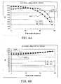
- FIG. 3Ais a graph of the intensity versus the duty cycle for a wire grid polarizer of an example embodiment.
- the wire grid polarizermay be of the type described in connection with FIG. 2 , for example, and having aluminum conductors 202 disposed over a fused silica substrate 201 .
- the data of the graph of FIGS. 3A and 3Bare from such a structure having a pitch of 140 nm, a height of 140 nm, normal incident light having a wavelength of 550 nm.
- the duty cycleis varied.
- the curve 301shows the transmittance of P-polarization state light
- the curve 302shows the reflectance of S-polarization state light.
- the transmittance T pdecreases with the duty cycle, and the reflectance R s increases with the duty cycle.
- the duty cycleis low, for example approaching approximately 0.0, the transmittance T p is approximately 97%; however, the reflectance R s is too low, only about 3%.
- the duty cycleis high, for example approaching approximately 1.00, the reflectance R s is high, close to 92%, but the transmittance T p is nearly 0%.
- the wire grid polarizeris not efficient in polarization recycling.
- a tradeoffmust be made between the transmittance T p and the reflectance R s to maximize the total light throughput, such as described by equation 1 or equation 3, by varying the ratio of the width to pitch, and the ratio of the height to pitch.
- FIG. 3Bis a graph of the merit functions versus the duty cycle in accordance with example embodiments.
- the data depicted in the graph of 3 Bare from the wire grid polarizer described in connection with the example embodiments of FIG. 3A .
- Curve 303shows the merit function (T 2 ) versus duty cycle for the wire grid polarizer disposed in a display system that effects polarization recycling via a quarter wave retarder and a reflecting elements, such as the system of the example embodiment of FIG. 1B .
- Curve 304shows the merit function (T 1 ) versus duty cycle for a wire grid polarizer implemented in a display system that provides light recycling using a diffusive reflector, such as the system of the example embodiment of FIG. 1A .
- the function of meritis substantially optimal at a duty cycle of approximately 0.18 to approximately 0.25, with a peak value at approximately 0.22 for each system.
- the total light output of a display including a wire grid polarizer and a light recycling by diffusion reflection of light of one polarization state or by polarization transformation and reflectionis optimal if the wire grid polarizer has a duty cycle of approximately 0.18 to approximately 0.25.
- the figures of merit for known devices having duty cycles of range of 0.40 to 0.60are significantly lower than the figures of merit (T 1 , T 2 ) of the wire grid polarizer of the example embodiments,.
- FIGS. 4A and 4Bshow graphically T 1 and T 2 vs. duty cycle with R varying from approximately 0.5 (50%) to approximately 1.0 (100%).
- the dataare computed from a wire grid structure as described in connection with an example embodiment having a pitch of approximately 140.0 nm, a height of approximately140.0 nm, and normally incident light having a wavelength of approximately 550 nm. It can be seen that the greater the value of R, the better are T 1 and T 2 . However, regardless of the value of R, the best values of T 1 and T 2 occur when the duty cycle is in approximately the range of approximately 0.18 to approximately 0.25. In other words, R does not significantly impact the dependence of T 1 and T 2 on the duty cycle. For simplicity, R is chosen to be 1 in the following discussion.
- Rhas been assumed to be 1 for simplified discussion.
- R scan be rescaled smaller to account for the impact of R.
- T 1 and T 2are beneficially improved, which clearly requires the improvement of the combination of the transmittance of the P-polarization (T p ) and the reflectance of the S-polarization (R s ).
- T pthe transmittance of the P-polarization
- R sthe reflectance of the S-polarization
- the data shown in FIGS. 3A , 3 B and 4 A through 4 B,are for normally incident light. In practice light comes from all directions in a given viewing cone. In this case, the total light throughput T 1 and T 2 are average values over the usable viewing cone. Nonetheless, applicants have discovered that although the absolute values of T 1 and T 2 may vary, the maximum total light throughput still is achieved with wire grid polarizer of example embodiments having a duty cycle of approximately 0.18 to approximately 0.25.
- FIGS. 5A and 5Bare graphical representations of the transmittance T p (%) and reflectance R s , respectively, as a function of incident wavelength for a wire grid polarizer according to example embodiments.
- the wire grid polarizerhas a pitch of approximately 140 nm and a duty cycle of approximately 0.20.
- the curve 501shows that the transmittance of the light of the transmitted P-polarization state is substantially maintained across the entire wavelength range.
- the reflectance of the light of the reflected polarization stateis shown by curve 502 and is substantially independent of the wavelength. Such performance is required in color display applications.
- FIGS. 6A and 6Bshow the transmittance T p (%) of the light of the transmitted polarization state and the reflectance R s (%) of the reflected polarization state, respectively, versus the angle of incidence ( ⁇ ) of wire grid polarizers.
- Curve 601is the transmittance versus ⁇ for a wire grid polarizer having a duty cycle of 0.45, whereas the curve 602 is the transmittance for a wire grid polarizer of an example embodiment having a duty cycle of 0.20.
- the transmittanceis substantially the same for the wire grid polarizer of an example embodiment having a duty cycle of approximately 0.20.
- the wire grid polarizer having a duty cycle of 0.20 in keeping with an illustrative embodimentprovided a nearly constant reflectance. This is compared to the reflectance shown by curve 604 , which is of a wire grid polarizer having a duty cycle of 0.45.
- FIGS. 6A and 6Balso show the tradeoff between the transmittance T p and reflectance R s needed to meet the desired performance in light recycling applications.
- the wire grid polarizer having a duty cycle of approximately 0.20has a much higher transmittance T p (approximately 97% at normal incidence or approximately 0 degree polar angle) than the one with a duty cycle of 0.45 (approximately 85% at normal incidence), though the wire grid polarizer having a duty cycle of 0.2 has a lower reflectance R s (about 84%) than the one with a duty cycle of 0.45 (about 88% at normal incidence).
- Overall the total light throughput based upon Eqns. 1, 2 or 3is higher for the wire grid polarizer with a duty cycle of 0.2 than the one with a duty cycle of 0.45, as discussed referring to FIG. 4 .
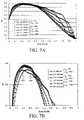
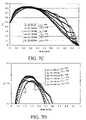
- FIGS. 7A and 7Care graphical representations of the merit function versus the duty cycle for a display device incorporating a quarter wave retarder (i.e., T 2 ) and a reflector for recycling and a display device incorporating a diffusive reflector for recycling (i.e., T 1 ), respectively.
- the duty cycle of the wire grid polarizersare in the range of approximately 0.0 to approximately 1.0.
- the incident lighthas a wavelength of approximately 550 nm
- the pitchis approximately 140 nm
- a number of wire grid polarizers having conductors of a variety of heightsare used.
- the curves 701 through 712represent the total light throughput of each of a variety of wire grid polarizers having the same pitch but varying duty cycle and having conductor heights (H) ranging from approximately 80 nm to approximately 200 nm.
- FIGS. 7A and 7Cprovide data of the effect of conductor height on the total transmittance over a range of duty cycles for each type of recycling system.
- FIGS. 7B and 7Dare exploded views of FIGS. 7A and 7C , respectively, for better view of the maximum total light throughput.
- the total light throughputis at a maximum level achieved according to the parameters of the present example embodiment.
- the heightis greater than approximately 200 nm, or less than approximately 80 nm, the total transmittance is reduced. This is indicated by the total light throughput T 1 or T 2 at approximately 200 nm as shown by curve 706 in FIG. 7B and curve 712 in FIG. 7D ; and approximately 80 nm as shown by curve 701 in FIG. 7B and curve 707 in FIG. 7D , which are lower than T 1 , or T 2 when the height is approximately 100 nm, approximately 120 nm, approximately 140 nm, or approximately 160 nm.
- FIG. 8shows a wire grid polarizer 800 in accordance with an example embodiment.
- the wire grid polarizer 800shows the conductors 202 that are substantially rectangular in cross-section, as well as conductors 801 that have imperfections due to manufacturing. As can be appreciated, these imperfections can create variances in the height, width and pitch of the wire grid polarizer 800 . Given these imperfections, the fill factor at each height z may be expressed as:
- the average fill factor over the entire height His given by:
- W av ⁇ S Hor W av ⁇ F.P. These are useful in determining the parameters for a wire grid polarizer having an average duty cycle in the range of approximately 0.18 to approximately 0.25.
- the display devices of the example embodiments of FIGS. 1A and 1Brealize an overall improvement in the light efficiency of approximately 10%.
- an additional improvement in light efficiency of approximately 4% to approximately 5%can be achieved by incorporating antireflection layer 901 .
- FIG. 9One example embodiment is shown in FIG. 9 , where antireflection layers 901 , 902 are disposed on either side of the substrate 201 of the wire grid polarizer 900 which further increases the transmittance T p of the light of P-polarization from 97% to up to 100% with little loss in reflectance R s . This example embodiment is shown in FIG. 9 .
- FIG. 10shows a low fill factor wire grid polarizer structure 1000 according to an example embodiment.
- the wire grid polarizeris integrated with the rear absorptive polarizer 1001 and shares a common substrate 201 .
- FIG. 11shows a further example embodiment 1100 wherein other optical components such as compensation films or retardation films can also be incorporated with the wire grid polarizer.
- FIG. 11depicts the wire grid elements 202 formed onto a substrate 201 .
- An absorptive polarizer layer 1001is shown with an additional functional layer 1101 .
- Layer 1101may comprise a compensation film, for example, although other functional layers could also be envisioned. While FIG. 11 does not indicate the presence of adhesive, barrier, or alignment layers, it can be appreciated that such additional layers would be found in the embodiment of FIG. 11 .
- the wire grid polarizeris disposed between the top and bottom substrates 1203 , 201 , respectively, of a liquid crystal display panel.
- a similar structure as shown in FIG. 11is depicted by wire grid assembly 1200 , with the wire grid elements 202 located directly on one surface of a substrate 201 of the liquid crystal cell.
- the liquid crystal material, electrodes, color filter and other panel elements and layersare not show, but are understood to be located on the same side of substrate 201 as the wire grid elements.
- a second wire grid polarizermay be used.
- the second wire grid polarizermay be substantially the same as one of the wire grid polarizers of the example embodiments.
- the second wire grid polarizer of assembly 1300is depicted by substrate 1301 and wire grid elements 1302 .
- This wire grid structureis shown adjacent to the example wire grid assembly of FIG. 12 .
- An air gap 1303is depicted between the wire grid structure on substrate 1301 and the liquid crystal panel substrate 1003 .
- This air gapis optional, and may be replaced by an adhesive, an index matching layer, or other material selected to produce optimal performance.
- the added wire grid comprising elements 1302 and substrate 1301are preferentially located on the backlight side of the liquid crystal panel.
- wire grids polarizersmay be used in a display provide an improved optical efficiency (illuminance) compared to known structures that include specular reflectors over certain surfaces of the light guide.
- optical efficiencyluminance
- known structuresthat include specular reflectors over certain surfaces of the light guide.
- the various methods, materials, components and parametersare included by way of example only and not in any limiting sense. Therefore, the embodiments described are illustrative and are useful in providing beneficial backlight assemblies. In view of this disclosure, those skilled in the art can implement the various example devices and methods to effect improved backlight efficiency, while remaining within the scope of the appended claims.
Landscapes
- Physics & Mathematics (AREA)
- General Physics & Mathematics (AREA)
- Optics & Photonics (AREA)
- Polarising Elements (AREA)
- Liquid Crystal (AREA)
- Projection Apparatus (AREA)
Abstract
Description
T2=0.5Tp(1+RRs) Eqn. 3
where w0(z) is the width of the wires at height z.
where
which is the area under the surface profile of the wire. From these expressions, the average width
or Wav≡F.P. These are useful in determining the parameters for a wire grid polarizer having an average duty cycle in the range of approximately 0.18 to approximately 0.25.
Claims (8)
Priority Applications (7)
| Application Number | Priority Date | Filing Date | Title |
|---|---|---|---|
| US10/948,345US7414784B2 (en) | 2004-09-23 | 2004-09-23 | Low fill factor wire grid polarizer and method of use |
| TW094128311ATWI380061B (en) | 2004-09-23 | 2005-08-19 | Low fill factor wire grid polarizer |
| CNB2005800322269ACN100495088C (en) | 2004-09-23 | 2005-09-13 | Low Duty Cycle Wire Grid Polarizers |
| KR1020077006583AKR20070065337A (en) | 2004-09-23 | 2005-09-13 | Low Fill Factor Wire Grid Polarizer |
| JP2007533535AJP4838804B2 (en) | 2004-09-23 | 2005-09-13 | Wire grid polarizer with low fill factor |
| PCT/US2005/032656WO2006036546A1 (en) | 2004-09-23 | 2005-09-13 | Low fill factor wire grid polarizer |
| US11/442,861US7466484B2 (en) | 2004-09-23 | 2006-05-30 | Wire grid polarizers and optical elements containing them |
Applications Claiming Priority (1)
| Application Number | Priority Date | Filing Date | Title |
|---|---|---|---|
| US10/948,345US7414784B2 (en) | 2004-09-23 | 2004-09-23 | Low fill factor wire grid polarizer and method of use |
Related Child Applications (1)
| Application Number | Title | Priority Date | Filing Date |
|---|---|---|---|
| US11/442,861Continuation-In-PartUS7466484B2 (en) | 2004-09-23 | 2006-05-30 | Wire grid polarizers and optical elements containing them |
Publications (2)
| Publication Number | Publication Date |
|---|---|
| US20060061862A1 US20060061862A1 (en) | 2006-03-23 |
| US7414784B2true US7414784B2 (en) | 2008-08-19 |
Family
ID=35457794
Family Applications (1)
| Application Number | Title | Priority Date | Filing Date |
|---|---|---|---|
| US10/948,345Expired - LifetimeUS7414784B2 (en) | 2004-09-23 | 2004-09-23 | Low fill factor wire grid polarizer and method of use |
Country Status (6)
| Country | Link |
|---|---|
| US (1) | US7414784B2 (en) |
| JP (1) | JP4838804B2 (en) |
| KR (1) | KR20070065337A (en) |
| CN (1) | CN100495088C (en) |
| TW (1) | TWI380061B (en) |
| WO (1) | WO2006036546A1 (en) |
Cited By (23)
| Publication number | Priority date | Publication date | Assignee | Title |
|---|---|---|---|---|
| US20080117510A1 (en)* | 2006-11-21 | 2008-05-22 | Samsung Electronics Co., Ltd. | Wire grid polarizer and method of manufacturing the same |
| US20080303986A1 (en)* | 2005-10-17 | 2008-12-11 | Hiroshi Yamaki | Wire grid polarizer and liquid crystal display device using the same |
| US20090052029A1 (en)* | 2006-10-12 | 2009-02-26 | Cambrios Technologies Corporation | Functional films formed by highly oriented deposition of nanowires |
| US20100302481A1 (en)* | 2009-06-01 | 2010-12-02 | Baum Alexandra | Absorbing wire grid polarizer |
| US7961393B2 (en) | 2004-12-06 | 2011-06-14 | Moxtek, Inc. | Selectively absorptive wire-grid polarizer |
| US20110273771A1 (en)* | 2009-01-13 | 2011-11-10 | Canon Kabushiki Kaisha | Optical element |
| US8248696B2 (en) | 2009-06-25 | 2012-08-21 | Moxtek, Inc. | Nano fractal diffuser |
| US20130258254A1 (en)* | 2012-03-30 | 2013-10-03 | Samsung Display Co., Ltd. | Liquid crystal display |
| US8587751B2 (en) | 2011-02-14 | 2013-11-19 | Samsung Electronics Co., Ltd. | Display panel and display apparatus having the same |
| US8611007B2 (en) | 2010-09-21 | 2013-12-17 | Moxtek, Inc. | Fine pitch wire grid polarizer |
| US8848141B2 (en) | 2011-02-14 | 2014-09-30 | Samsung Electronics Co., Ltd. | Display panel and display apparatus having the same |
| US8873144B2 (en) | 2011-05-17 | 2014-10-28 | Moxtek, Inc. | Wire grid polarizer with multiple functionality sections |
| US8913320B2 (en) | 2011-05-17 | 2014-12-16 | Moxtek, Inc. | Wire grid polarizer with bordered sections |
| US8913321B2 (en) | 2010-09-21 | 2014-12-16 | Moxtek, Inc. | Fine pitch grid polarizer |
| US8922890B2 (en) | 2012-03-21 | 2014-12-30 | Moxtek, Inc. | Polarizer edge rib modification |
| US8947772B2 (en) | 2006-08-31 | 2015-02-03 | Moxtek, Inc. | Durable, inorganic, absorptive, ultra-violet, grid polarizer |
| US8964012B2 (en) | 2011-02-14 | 2015-02-24 | Samsung Electronics Co., Ltd. | Display panel having a polarizing layer and display apparatus having the same |
| US9348076B2 (en) | 2013-10-24 | 2016-05-24 | Moxtek, Inc. | Polarizer with variable inter-wire distance |
| US9632224B2 (en) | 2014-06-25 | 2017-04-25 | Moxtek, Inc. | Broadband, selectively-absorptive wire grid polarizer |
| US9684203B2 (en) | 2014-06-25 | 2017-06-20 | Moxtek, Inc. | Wire grid polarizer with dual absorptive regions |
| US9696589B2 (en) | 2014-01-13 | 2017-07-04 | Samsung Electronics Co., Ltd. | In-cell polarizer, liquid crystal display including the same, and method of manufacturing liquid crystal display |
| US10175401B2 (en) | 2015-11-12 | 2019-01-08 | Moxtek, Inc. | Dual-purpose, absorptive, reflective wire grid polarizer |
| US20220381963A1 (en)* | 2021-06-01 | 2022-12-01 | Moxtek, Inc. | Optical Device with a Flexible, Opaque-Region |
Families Citing this family (58)
| Publication number | Priority date | Publication date | Assignee | Title |
|---|---|---|---|---|
| JP3972919B2 (en)* | 2004-04-19 | 2007-09-05 | コニカミノルタホールディングス株式会社 | Method for manufacturing birefringent optical element |
| JP2006003384A (en)* | 2004-06-15 | 2006-01-05 | Sony Corp | Polarizing beam splitter and liquid crystal projector device |
| US7466484B2 (en)* | 2004-09-23 | 2008-12-16 | Rohm And Haas Denmark Finance A/S | Wire grid polarizers and optical elements containing them |
| US7457037B2 (en)* | 2004-09-27 | 2008-11-25 | Corning Incorporated | Transparent polarizing optical products and fabrication thereof |
| JP4506412B2 (en)* | 2004-10-28 | 2010-07-21 | ウシオ電機株式会社 | Polarizing element unit and polarized light irradiation device |
| KR20060042481A (en)* | 2004-11-09 | 2006-05-15 | 엘지전자 주식회사 | Liquid Crystal Display Including Reflective Polarizer |
| US20080055719A1 (en)* | 2006-08-31 | 2008-03-06 | Perkins Raymond T | Inorganic, Dielectric Grid Polarizer |
| US20080055720A1 (en)* | 2006-08-31 | 2008-03-06 | Perkins Raymond T | Optical Data Storage System with an Inorganic, Dielectric Grid Polarizer |
| US7800823B2 (en)* | 2004-12-06 | 2010-09-21 | Moxtek, Inc. | Polarization device to polarize and further control light |
| US20080055549A1 (en)* | 2006-08-31 | 2008-03-06 | Perkins Raymond T | Projection Display with an Inorganic, Dielectric Grid Polarizer |
| US20080055721A1 (en)* | 2006-08-31 | 2008-03-06 | Perkins Raymond T | Light Recycling System with an Inorganic, Dielectric Grid Polarizer |
| US7570424B2 (en)* | 2004-12-06 | 2009-08-04 | Moxtek, Inc. | Multilayer wire-grid polarizer |
| US7630133B2 (en)* | 2004-12-06 | 2009-12-08 | Moxtek, Inc. | Inorganic, dielectric, grid polarizer and non-zero order diffraction grating |
| US20080055722A1 (en)* | 2006-08-31 | 2008-03-06 | Perkins Raymond T | Optical Polarization Beam Combiner/Splitter with an Inorganic, Dielectric Grid Polarizer |
| JP4889239B2 (en)* | 2005-05-18 | 2012-03-07 | チェイル インダストリーズ インコーポレイテッド | Backlight unit and liquid crystal display device |
| KR20070010472A (en)* | 2005-07-19 | 2007-01-24 | 삼성전자주식회사 | Hybrid polarizer, manufacturing method thereof and display device having same |
| TWI273287B (en)* | 2005-07-29 | 2007-02-11 | Taiwan Tft Lcd Ass | Integrated type optical film with wire grid polarizer structure and manufacturing method thereof |
| US7458687B2 (en) | 2006-05-26 | 2008-12-02 | Eastman Kodak Company | High efficiency digital cinema projection system with increased etendue |
| US20070273797A1 (en)* | 2006-05-26 | 2007-11-29 | Silverstein Barry D | High efficiency digital cinema projection system with increased etendue |
| US20070273798A1 (en)* | 2006-05-26 | 2007-11-29 | Silverstein Barry D | High efficiency digital cinema projection system with increased etendue |
| US20080038467A1 (en)* | 2006-08-11 | 2008-02-14 | Eastman Kodak Company | Nanostructured pattern method of manufacture |
| KR101294004B1 (en)* | 2006-11-02 | 2013-08-07 | 삼성디스플레이 주식회사 | Polarizing substrate, display panel and display device having the same |
| JP5096735B2 (en)* | 2006-12-05 | 2012-12-12 | Jx日鉱日石エネルギー株式会社 | Wire grid polarizer and method for manufacturing the same, and retardation film and liquid crystal display device using the same |
| JP4488033B2 (en)* | 2007-02-06 | 2010-06-23 | ソニー株式会社 | Polarizing element and liquid crystal projector |
| JP5010527B2 (en)* | 2007-06-04 | 2012-08-29 | 住友化学株式会社 | Light guide plate unit, surface light source device, and liquid crystal display device |
| JP2009003106A (en)* | 2007-06-20 | 2009-01-08 | Sony Corp | Liquid crystal display |
| KR101372848B1 (en)* | 2007-07-19 | 2014-03-10 | 성균관대학교산학협력단 | Method for manufacturing metal line grid device |
| WO2009018107A1 (en)* | 2007-08-02 | 2009-02-05 | Agoura Technologies, Inc. | Nanoembossed shapes and fabrication methods of wire grid polarizers |
| US20090059367A1 (en)* | 2007-08-30 | 2009-03-05 | O'malley Shawn Michael | Light-polarizing article and process for making same |
| JP4507126B2 (en)* | 2007-10-29 | 2010-07-21 | ソニー株式会社 | Manufacturing method of polarizing plate |
| US8169685B2 (en) | 2007-12-20 | 2012-05-01 | Ravenbrick, Llc | Thermally switched absorptive window shutter |
| CA2754619C (en)* | 2008-04-23 | 2014-04-01 | Ravenbrick, Llc | Glare management of reflective and thermoreflective surfaces |
| US9116302B2 (en) | 2008-06-19 | 2015-08-25 | Ravenbrick Llc | Optical metapolarizer device |
| JP5497364B2 (en)* | 2008-08-05 | 2014-05-21 | 旭化成イーマテリアルズ株式会社 | Manufacturing method of wire grid polarizing plate |
| EP2324386A4 (en) | 2008-08-20 | 2013-03-27 | Ravenbrick Llc | Methods for fabricating thermochromic filters |
| US8310757B2 (en)* | 2008-08-28 | 2012-11-13 | Smartershade, Inc. | Wire grid polarizers in window shading applications and varying thickness wave retarders |
| US20100103517A1 (en)* | 2008-10-29 | 2010-04-29 | Mark Alan Davis | Segmented film deposition |
| US8013954B2 (en)* | 2009-02-17 | 2011-09-06 | Sharp Kabushiki Kaisha | Liquid crystal display |
| JP5527074B2 (en)* | 2009-11-16 | 2014-06-18 | セイコーエプソン株式会社 | Polarizing element and projector |
| WO2011062708A2 (en) | 2009-11-17 | 2011-05-26 | Ravenbrick Llc | Thermally switched optical filter incorporating a refractive optical structure |
| JP5526851B2 (en)* | 2010-02-19 | 2014-06-18 | セイコーエプソン株式会社 | Polarizing element and projector |
| JP5463947B2 (en)* | 2010-02-19 | 2014-04-09 | セイコーエプソン株式会社 | Polarizing element and projector |
| US20120161344A1 (en) | 2010-12-27 | 2012-06-28 | Skc Haas Display Films Co., Ltd. | Method of manufacturing a diffusely-reflecting polarizer having a nearly isotropic continuous phase |
| KR20130137668A (en) | 2010-12-30 | 2013-12-17 | 스마터쉐이드, 인코포레이티드 | Variable transmittance window |
| CN102540306B (en) | 2010-12-31 | 2015-03-25 | 北京京东方光电科技有限公司 | Grating, liquid crystal display device and manufacture methods of grating and liquid crystal display device |
| JP2012238632A (en)* | 2011-05-10 | 2012-12-06 | Sony Corp | Solid-state imaging device, method of manufacturing the same, and electronic apparatus |
| JP5938241B2 (en)* | 2012-03-15 | 2016-06-22 | 日立マクセル株式会社 | Optical element and manufacturing method thereof |
| WO2013190680A1 (en)* | 2012-06-21 | 2013-12-27 | 日立コンシューマエレクトロニクス株式会社 | Optical element and optical device |
| JP6047051B2 (en)* | 2013-03-28 | 2016-12-21 | 日立マクセル株式会社 | Optical element and optical device |
| US20150055057A1 (en)* | 2013-08-23 | 2015-02-26 | Austin L. Huang | Touch sensitive display |
| US10082675B2 (en)* | 2014-10-21 | 2018-09-25 | Reald Inc. | High power handling polarization switches |
| US9450203B2 (en)* | 2014-12-22 | 2016-09-20 | Apple Inc. | Organic light-emitting diode display with glass encapsulation and peripheral welded plastic seal |
| JP6610129B2 (en)* | 2015-09-29 | 2019-11-27 | 大日本印刷株式会社 | Liquid crystal display |
| GB2546150A (en) | 2015-11-23 | 2017-07-12 | Vg Smartglass Llc | Variable transmission window including blackout bars |
| US10139537B2 (en) | 2016-11-22 | 2018-11-27 | Moxtek, Inc. | Multiple-stack wire grid polarizer |
| JP6922279B2 (en)* | 2017-03-14 | 2021-08-18 | セイコーエプソン株式会社 | Wire grid polarizing element and projection type display device |
| US20190154904A1 (en)* | 2017-11-21 | 2019-05-23 | Wuhan China Star Optoelectronics Technology Co., Ltd. | Array substrate and fabricating method thereof, flexible display panel, and flexible display device |
| JP2020098259A (en)* | 2018-12-18 | 2020-06-25 | セイコーエプソン株式会社 | Display and reflection type polarization element |
Citations (17)
| Publication number | Priority date | Publication date | Assignee | Title |
|---|---|---|---|---|
| US4688897A (en) | 1985-06-17 | 1987-08-25 | Hughes Aircraft Company | Liquid crystal device |
| WO1994011766A1 (en) | 1992-11-09 | 1994-05-26 | Honeywell Inc. | A reflective polarizer |
| US5748368A (en) | 1994-12-29 | 1998-05-05 | Sony Corporation | Polarization optical element |
| US5986730A (en) | 1998-12-01 | 1999-11-16 | Moxtek | Dual mode reflective/transmissive liquid crystal display apparatus |
| US6108131A (en) | 1998-05-14 | 2000-08-22 | Moxtek | Polarizer apparatus for producing a generally polarized beam of light |
| US6208463B1 (en) | 1998-05-14 | 2001-03-27 | Moxtek | Polarizer apparatus for producing a generally polarized beam of light |
| US6243199B1 (en) | 1999-09-07 | 2001-06-05 | Moxtek | Broad band wire grid polarizing beam splitter for use in the visible wavelength region |
| US6288840B1 (en) | 1999-06-22 | 2001-09-11 | Moxtek | Imbedded wire grid polarizer for the visible spectrum |
| EP1180711A1 (en) | 2000-01-28 | 2002-02-20 | Seiko Epson Corporation | Optical reflection polarizer and projector comprising the same |
| US6486997B1 (en)* | 1997-10-28 | 2002-11-26 | 3M Innovative Properties Company | Reflective LCD projection system using wide-angle Cartesian polarizing beam splitter |
| US6532111B2 (en) | 2001-03-05 | 2003-03-11 | Eastman Kodak Company | Wire grid polarizer |
| US6590695B1 (en)* | 2002-02-26 | 2003-07-08 | Eastman Kodak Company | Micro-mechanical polarization-based modulator |
| US6665119B1 (en)* | 2002-10-15 | 2003-12-16 | Eastman Kodak Company | Wire grid polarizer |
| WO2004019070A2 (en) | 2002-08-21 | 2004-03-04 | Nanoopto Corporation | Method and system for providing beam polarization |
| US20040174596A1 (en) | 2003-03-05 | 2004-09-09 | Ricoh Optical Industries Co., Ltd. | Polarization optical device and manufacturing method therefor |
| US20050018309A1 (en)* | 2003-05-22 | 2005-01-27 | Mcguire James R. | Apparatus and methods for illuminating optical systems |
| US20060127830A1 (en)* | 2004-12-15 | 2006-06-15 | Xuegong Deng | Structures for polarization and beam control |
Family Cites Families (6)
| Publication number | Priority date | Publication date | Assignee | Title |
|---|---|---|---|---|
| WO1993023574A1 (en)* | 1992-05-14 | 1993-11-25 | Kozal Michael J | Polymerase chain reaction assays for monitoring antiviral therapy |
| JPH0990122A (en)* | 1995-09-28 | 1997-04-04 | Kyocera Corp | Method for manufacturing grid-type polarizer |
| US6122103A (en)* | 1999-06-22 | 2000-09-19 | Moxtech | Broadband wire grid polarizer for the visible spectrum |
| JP2003215344A (en)* | 2001-03-29 | 2003-07-30 | Seiko Epson Corp | Polarizer and optical device using the polarizer |
| US6747799B2 (en)* | 2001-11-12 | 2004-06-08 | Pts Corporation | High-efficiency low-polarization-dependent-loss lamellar diffraction-grating profile and production process |
| JP4376507B2 (en)* | 2002-11-01 | 2009-12-02 | リコー光学株式会社 | Polarizing optical element |
- 2004
- 2004-09-23USUS10/948,345patent/US7414784B2/ennot_activeExpired - Lifetime
- 2005
- 2005-08-19TWTW094128311Apatent/TWI380061B/ennot_activeIP Right Cessation
- 2005-09-13KRKR1020077006583Apatent/KR20070065337A/ennot_activeCeased
- 2005-09-13JPJP2007533535Apatent/JP4838804B2/ennot_activeExpired - Fee Related
- 2005-09-13WOPCT/US2005/032656patent/WO2006036546A1/enactiveApplication Filing
- 2005-09-13CNCNB2005800322269Apatent/CN100495088C/ennot_activeExpired - Fee Related
Patent Citations (18)
| Publication number | Priority date | Publication date | Assignee | Title |
|---|---|---|---|---|
| US4688897A (en) | 1985-06-17 | 1987-08-25 | Hughes Aircraft Company | Liquid crystal device |
| WO1994011766A1 (en) | 1992-11-09 | 1994-05-26 | Honeywell Inc. | A reflective polarizer |
| US5748368A (en) | 1994-12-29 | 1998-05-05 | Sony Corporation | Polarization optical element |
| US6486997B1 (en)* | 1997-10-28 | 2002-11-26 | 3M Innovative Properties Company | Reflective LCD projection system using wide-angle Cartesian polarizing beam splitter |
| US6108131A (en) | 1998-05-14 | 2000-08-22 | Moxtek | Polarizer apparatus for producing a generally polarized beam of light |
| US6208463B1 (en) | 1998-05-14 | 2001-03-27 | Moxtek | Polarizer apparatus for producing a generally polarized beam of light |
| US5986730A (en) | 1998-12-01 | 1999-11-16 | Moxtek | Dual mode reflective/transmissive liquid crystal display apparatus |
| US6288840B1 (en) | 1999-06-22 | 2001-09-11 | Moxtek | Imbedded wire grid polarizer for the visible spectrum |
| US6243199B1 (en) | 1999-09-07 | 2001-06-05 | Moxtek | Broad band wire grid polarizing beam splitter for use in the visible wavelength region |
| EP1180711A1 (en) | 2000-01-28 | 2002-02-20 | Seiko Epson Corporation | Optical reflection polarizer and projector comprising the same |
| US6592224B2 (en)* | 2000-01-28 | 2003-07-15 | Seiko Epson Corporation | Optical reflection polarizer and projector comprising the same |
| US6532111B2 (en) | 2001-03-05 | 2003-03-11 | Eastman Kodak Company | Wire grid polarizer |
| US6590695B1 (en)* | 2002-02-26 | 2003-07-08 | Eastman Kodak Company | Micro-mechanical polarization-based modulator |
| WO2004019070A2 (en) | 2002-08-21 | 2004-03-04 | Nanoopto Corporation | Method and system for providing beam polarization |
| US6665119B1 (en)* | 2002-10-15 | 2003-12-16 | Eastman Kodak Company | Wire grid polarizer |
| US20040174596A1 (en) | 2003-03-05 | 2004-09-09 | Ricoh Optical Industries Co., Ltd. | Polarization optical device and manufacturing method therefor |
| US20050018309A1 (en)* | 2003-05-22 | 2005-01-27 | Mcguire James R. | Apparatus and methods for illuminating optical systems |
| US20060127830A1 (en)* | 2004-12-15 | 2006-06-15 | Xuegong Deng | Structures for polarization and beam control |
Non-Patent Citations (4)
| Title |
|---|
| Kazutaka Baba and Mitsunobu Miyagi, "Optial polarizer using anisotrpoic metallic island films with a large aperature and a high extinction ratio", Optics Letters, OSA, vol. 16, No. 12, Jun. 15, 1991, pp. 964-966. |
| Michael A. Jensen and Gregory P. Nordin, "Characterization of two-dimensional finite-aperature wire grid polarizers by a spectral-domain technique", Applied Optics, vol. 40, No. 26, Sep. 10, 2001, pp. 4738-4745. |
| Michael A. Jensen and Gregory P. Nordin, "Finite-aperature wire grid polarizers", Journal of the Optical Society of America, vol. 17, No. 12, Dec. 2000, pp. 2191-2198. |
| W.G. Driscoll et al., "Polarization", Handbook of Optica, 1978, pp. 10-72 to 19-77 (See p. 72, last paragraph). |
Cited By (30)
| Publication number | Priority date | Publication date | Assignee | Title |
|---|---|---|---|---|
| US7961393B2 (en) | 2004-12-06 | 2011-06-14 | Moxtek, Inc. | Selectively absorptive wire-grid polarizer |
| US20080303986A1 (en)* | 2005-10-17 | 2008-12-11 | Hiroshi Yamaki | Wire grid polarizer and liquid crystal display device using the same |
| US7894019B2 (en)* | 2005-10-17 | 2011-02-22 | Asahi Kasei Kabushiki Kaisha | Wire grid polarizer and liquid crystal display device using the same |
| US8947772B2 (en) | 2006-08-31 | 2015-02-03 | Moxtek, Inc. | Durable, inorganic, absorptive, ultra-violet, grid polarizer |
| US20090052029A1 (en)* | 2006-10-12 | 2009-02-26 | Cambrios Technologies Corporation | Functional films formed by highly oriented deposition of nanowires |
| US8014068B2 (en)* | 2006-11-21 | 2011-09-06 | Samsung Electronics Co., Ltd. | Wire grid polarizer and method of manufacturing the same |
| US20080117510A1 (en)* | 2006-11-21 | 2008-05-22 | Samsung Electronics Co., Ltd. | Wire grid polarizer and method of manufacturing the same |
| US9097906B2 (en)* | 2009-01-13 | 2015-08-04 | Canon Kabushiki Kaisha | Optical element |
| US20110273771A1 (en)* | 2009-01-13 | 2011-11-10 | Canon Kabushiki Kaisha | Optical element |
| US20100302481A1 (en)* | 2009-06-01 | 2010-12-02 | Baum Alexandra | Absorbing wire grid polarizer |
| US8248696B2 (en) | 2009-06-25 | 2012-08-21 | Moxtek, Inc. | Nano fractal diffuser |
| US8611007B2 (en) | 2010-09-21 | 2013-12-17 | Moxtek, Inc. | Fine pitch wire grid polarizer |
| US9523805B2 (en) | 2010-09-21 | 2016-12-20 | Moxtek, Inc. | Fine pitch wire grid polarizer |
| US8913321B2 (en) | 2010-09-21 | 2014-12-16 | Moxtek, Inc. | Fine pitch grid polarizer |
| US8848141B2 (en) | 2011-02-14 | 2014-09-30 | Samsung Electronics Co., Ltd. | Display panel and display apparatus having the same |
| US8587751B2 (en) | 2011-02-14 | 2013-11-19 | Samsung Electronics Co., Ltd. | Display panel and display apparatus having the same |
| US8964012B2 (en) | 2011-02-14 | 2015-02-24 | Samsung Electronics Co., Ltd. | Display panel having a polarizing layer and display apparatus having the same |
| US8913320B2 (en) | 2011-05-17 | 2014-12-16 | Moxtek, Inc. | Wire grid polarizer with bordered sections |
| US8873144B2 (en) | 2011-05-17 | 2014-10-28 | Moxtek, Inc. | Wire grid polarizer with multiple functionality sections |
| US8922890B2 (en) | 2012-03-21 | 2014-12-30 | Moxtek, Inc. | Polarizer edge rib modification |
| US20130258254A1 (en)* | 2012-03-30 | 2013-10-03 | Samsung Display Co., Ltd. | Liquid crystal display |
| US9348076B2 (en) | 2013-10-24 | 2016-05-24 | Moxtek, Inc. | Polarizer with variable inter-wire distance |
| US9354374B2 (en) | 2013-10-24 | 2016-05-31 | Moxtek, Inc. | Polarizer with wire pair over rib |
| US9632223B2 (en) | 2013-10-24 | 2017-04-25 | Moxtek, Inc. | Wire grid polarizer with side region |
| US9696589B2 (en) | 2014-01-13 | 2017-07-04 | Samsung Electronics Co., Ltd. | In-cell polarizer, liquid crystal display including the same, and method of manufacturing liquid crystal display |
| US9632224B2 (en) | 2014-06-25 | 2017-04-25 | Moxtek, Inc. | Broadband, selectively-absorptive wire grid polarizer |
| US9684203B2 (en) | 2014-06-25 | 2017-06-20 | Moxtek, Inc. | Wire grid polarizer with dual absorptive regions |
| US9869898B2 (en) | 2014-06-25 | 2018-01-16 | Moxtek, Inc. | Wire grid polarizer with dual absorptive regions |
| US10175401B2 (en) | 2015-11-12 | 2019-01-08 | Moxtek, Inc. | Dual-purpose, absorptive, reflective wire grid polarizer |
| US20220381963A1 (en)* | 2021-06-01 | 2022-12-01 | Moxtek, Inc. | Optical Device with a Flexible, Opaque-Region |
Also Published As
| Publication number | Publication date |
|---|---|
| TWI380061B (en) | 2012-12-21 |
| TW200619697A (en) | 2006-06-16 |
| JP4838804B2 (en) | 2011-12-14 |
| US20060061862A1 (en) | 2006-03-23 |
| KR20070065337A (en) | 2007-06-22 |
| WO2006036546A1 (en) | 2006-04-06 |
| CN101027578A (en) | 2007-08-29 |
| JP2008514996A (en) | 2008-05-08 |
| CN100495088C (en) | 2009-06-03 |
Similar Documents
| Publication | Publication Date | Title |
|---|---|---|
| US7414784B2 (en) | Low fill factor wire grid polarizer and method of use | |
| US7466484B2 (en) | Wire grid polarizers and optical elements containing them | |
| US7233563B2 (en) | Polarizing optical element and display device including the same | |
| TW565733B (en) | Liquid crystal display device | |
| JP3917417B2 (en) | Reflective liquid crystal display | |
| US6888678B2 (en) | Irregular-shape body, reflection sheet and reflection-type liquid crystal display element, and production method and production device therefor | |
| JP4292596B2 (en) | Diffuse reflector, manufacturing method thereof and display device | |
| US20100302481A1 (en) | Absorbing wire grid polarizer | |
| US20090148616A1 (en) | Reflection type liquid crystal display device and manufacturing method thereof | |
| JP4118027B2 (en) | Liquid crystal display | |
| TWI728338B (en) | Display panel | |
| US20020075434A1 (en) | Cholesteric liquid crystal polarizing device | |
| US6433847B1 (en) | Reflection liquid crystal display which includes a pair of substrates | |
| US20060269214A1 (en) | Light management films of differing refractive indices | |
| US9080748B2 (en) | Display panel having improved light-use efficiency, display device including the display panel, and method of manufacturing the display panel | |
| US20050276073A1 (en) | Diffusive reflector films for enhanced liquid crystal display efficiency | |
| JPH09146092A (en) | Lighting device and liquid crystal display device using the same | |
| JPH10319391A (en) | Diffusion reflection plate and its production and reflection type guest-host liquid crystal display device | |
| JP4510797B2 (en) | Reflective liquid crystal display | |
| JP3899880B2 (en) | Liquid crystal display |
Legal Events
| Date | Code | Title | Description |
|---|---|---|---|
| AS | Assignment | Owner name:EASTMAN KODAK COMPANY, NEW YORK Free format text:ASSIGNMENT OF ASSIGNORS INTEREST;ASSIGNORS:MI, XIANG-DONG;KESSLER, DAVID;TUTT, LEE W.;AND OTHERS;REEL/FRAME:015834/0699 Effective date:20040923 | |
| AS | Assignment | Owner name:ROHM AND HAAS DENMARK FINANCE A/S, DENMARK Free format text:ASSIGNMENT OF ASSIGNORS INTEREST;ASSIGNOR:EASTMAN KODAK COMPANY;REEL/FRAME:019830/0780 Effective date:20070628 Owner name:ROHM AND HAAS DENMARK FINANCE A/S,DENMARK Free format text:ASSIGNMENT OF ASSIGNORS INTEREST;ASSIGNOR:EASTMAN KODAK COMPANY;REEL/FRAME:019830/0780 Effective date:20070628 | |
| STCF | Information on status: patent grant | Free format text:PATENTED CASE | |
| AS | Assignment | Owner name:SKC HAAS DISPLAY FILMS CO., LTD., KOREA, REPUBLIC Free format text:ASSIGNMENT OF ASSIGNORS INTEREST;ASSIGNOR:ROHM AND HAAS DENMARK FINANCE A/S;REEL/FRAME:022259/0956 Effective date:20090126 Owner name:SKC HAAS DISPLAY FILMS CO., LTD.,KOREA, REPUBLIC O Free format text:ASSIGNMENT OF ASSIGNORS INTEREST;ASSIGNOR:ROHM AND HAAS DENMARK FINANCE A/S;REEL/FRAME:022259/0956 Effective date:20090126 | |
| FPAY | Fee payment | Year of fee payment:4 | |
| FPAY | Fee payment | Year of fee payment:8 | |
| AS | Assignment | Owner name:NAME: SKC HI-TECH & MARKETING CO., LTD., KOREA, RE Free format text:CHANGE OF NAME;ASSIGNOR:SKC HAAS DISPLAY FILMS CO., LTD.;REEL/FRAME:043479/0570 Effective date:20170707 | |
| AS | Assignment | Owner name:SKC HI-TECH & MARKETING CO., LTD. (COMPANY REGISTR Free format text:ASSIGNMENT OF ASSIGNORS INTEREST;ASSIGNOR:SKC HI-TECH & MARKETING CO., LTD. (COMPANY REGISTRATION NO. 161514-0001344);REEL/FRAME:045616/0157 Effective date:20180227 | |
| MAFP | Maintenance fee payment | Free format text:PAYMENT OF MAINTENANCE FEE, 12TH YEAR, LARGE ENTITY (ORIGINAL EVENT CODE: M1553); ENTITY STATUS OF PATENT OWNER: LARGE ENTITY Year of fee payment:12 | |
| AS | Assignment | Owner name:SK MICROWORKS SOLUTIONS CO., LTD., KOREA, REPUBLIC OF Free format text:CHANGE OF NAME;ASSIGNOR:SKC HI-TECH & MARKETING CO., LTD.;REEL/FRAME:062447/0345 Effective date:20180102 |