US7414600B2 - Pixel current driver for organic light emitting diode displays - Google Patents
Pixel current driver for organic light emitting diode displaysDownload PDFInfo
- Publication number
- US7414600B2 US7414600B2US11/247,455US24745505AUS7414600B2US 7414600 B2US7414600 B2US 7414600B2US 24745505 AUS24745505 AUS 24745505AUS 7414600 B2US7414600 B2US 7414600B2
- Authority
- US
- United States
- Prior art keywords
- thin film
- gate
- transistor
- pixel
- current
- Prior art date
- Legal status (The legal status is an assumption and is not a legal conclusion. Google has not performed a legal analysis and makes no representation as to the accuracy of the status listed.)
- Expired - Lifetime, expires
Links
Images


Classifications
- G—PHYSICS
- G09—EDUCATION; CRYPTOGRAPHY; DISPLAY; ADVERTISING; SEALS
- G09G—ARRANGEMENTS OR CIRCUITS FOR CONTROL OF INDICATING DEVICES USING STATIC MEANS TO PRESENT VARIABLE INFORMATION
- G09G3/00—Control arrangements or circuits, of interest only in connection with visual indicators other than cathode-ray tubes
- G09G3/20—Control arrangements or circuits, of interest only in connection with visual indicators other than cathode-ray tubes for presentation of an assembly of a number of characters, e.g. a page, by composing the assembly by combination of individual elements arranged in a matrix no fixed position being assigned to or needed to be assigned to the individual characters or partial characters
- G09G3/22—Control arrangements or circuits, of interest only in connection with visual indicators other than cathode-ray tubes for presentation of an assembly of a number of characters, e.g. a page, by composing the assembly by combination of individual elements arranged in a matrix no fixed position being assigned to or needed to be assigned to the individual characters or partial characters using controlled light sources
- G09G3/30—Control arrangements or circuits, of interest only in connection with visual indicators other than cathode-ray tubes for presentation of an assembly of a number of characters, e.g. a page, by composing the assembly by combination of individual elements arranged in a matrix no fixed position being assigned to or needed to be assigned to the individual characters or partial characters using controlled light sources using electroluminescent panels
- G09G3/32—Control arrangements or circuits, of interest only in connection with visual indicators other than cathode-ray tubes for presentation of an assembly of a number of characters, e.g. a page, by composing the assembly by combination of individual elements arranged in a matrix no fixed position being assigned to or needed to be assigned to the individual characters or partial characters using controlled light sources using electroluminescent panels semiconductive, e.g. using light-emitting diodes [LED]
- G09G3/3208—Control arrangements or circuits, of interest only in connection with visual indicators other than cathode-ray tubes for presentation of an assembly of a number of characters, e.g. a page, by composing the assembly by combination of individual elements arranged in a matrix no fixed position being assigned to or needed to be assigned to the individual characters or partial characters using controlled light sources using electroluminescent panels semiconductive, e.g. using light-emitting diodes [LED] organic, e.g. using organic light-emitting diodes [OLED]
- G09G3/3225—Control arrangements or circuits, of interest only in connection with visual indicators other than cathode-ray tubes for presentation of an assembly of a number of characters, e.g. a page, by composing the assembly by combination of individual elements arranged in a matrix no fixed position being assigned to or needed to be assigned to the individual characters or partial characters using controlled light sources using electroluminescent panels semiconductive, e.g. using light-emitting diodes [LED] organic, e.g. using organic light-emitting diodes [OLED] using an active matrix
- G09G3/3233—Control arrangements or circuits, of interest only in connection with visual indicators other than cathode-ray tubes for presentation of an assembly of a number of characters, e.g. a page, by composing the assembly by combination of individual elements arranged in a matrix no fixed position being assigned to or needed to be assigned to the individual characters or partial characters using controlled light sources using electroluminescent panels semiconductive, e.g. using light-emitting diodes [LED] organic, e.g. using organic light-emitting diodes [OLED] using an active matrix with pixel circuitry controlling the current through the light-emitting element
- G09G3/3241—Control arrangements or circuits, of interest only in connection with visual indicators other than cathode-ray tubes for presentation of an assembly of a number of characters, e.g. a page, by composing the assembly by combination of individual elements arranged in a matrix no fixed position being assigned to or needed to be assigned to the individual characters or partial characters using controlled light sources using electroluminescent panels semiconductive, e.g. using light-emitting diodes [LED] organic, e.g. using organic light-emitting diodes [OLED] using an active matrix with pixel circuitry controlling the current through the light-emitting element the current through the light-emitting element being set using a data current provided by the data driver, e.g. by using a two-transistor current mirror
- H—ELECTRICITY
- H10—SEMICONDUCTOR DEVICES; ELECTRIC SOLID-STATE DEVICES NOT OTHERWISE PROVIDED FOR
- H10K—ORGANIC ELECTRIC SOLID-STATE DEVICES
- H10K59/00—Integrated devices, or assemblies of multiple devices, comprising at least one organic light-emitting element covered by group H10K50/00
- H10K59/10—OLED displays
- H10K59/12—Active-matrix OLED [AMOLED] displays
- H10K59/131—Interconnections, e.g. wiring lines or terminals
- G—PHYSICS
- G09—EDUCATION; CRYPTOGRAPHY; DISPLAY; ADVERTISING; SEALS
- G09G—ARRANGEMENTS OR CIRCUITS FOR CONTROL OF INDICATING DEVICES USING STATIC MEANS TO PRESENT VARIABLE INFORMATION
- G09G2300/00—Aspects of the constitution of display devices
- G09G2300/08—Active matrix structure, i.e. with use of active elements, inclusive of non-linear two terminal elements, in the pixels together with light emitting or modulating elements
- G09G2300/0804—Sub-multiplexed active matrix panel, i.e. wherein one active driving circuit is used at pixel level for multiple image producing elements
- G—PHYSICS
- G09—EDUCATION; CRYPTOGRAPHY; DISPLAY; ADVERTISING; SEALS
- G09G—ARRANGEMENTS OR CIRCUITS FOR CONTROL OF INDICATING DEVICES USING STATIC MEANS TO PRESENT VARIABLE INFORMATION
- G09G2320/00—Control of display operating conditions
- G09G2320/02—Improving the quality of display appearance
- G09G2320/0223—Compensation for problems related to R-C delay and attenuation in electrodes of matrix panels, e.g. in gate electrodes or on-substrate video signal electrodes
- H—ELECTRICITY
- H10—SEMICONDUCTOR DEVICES; ELECTRIC SOLID-STATE DEVICES NOT OTHERWISE PROVIDED FOR
- H10D—INORGANIC ELECTRIC SEMICONDUCTOR DEVICES
- H10D86/00—Integrated devices formed in or on insulating or conducting substrates, e.g. formed in silicon-on-insulator [SOI] substrates or on stainless steel or glass substrates
- H—ELECTRICITY
- H10—SEMICONDUCTOR DEVICES; ELECTRIC SOLID-STATE DEVICES NOT OTHERWISE PROVIDED FOR
- H10K—ORGANIC ELECTRIC SOLID-STATE DEVICES
- H10K19/00—Integrated devices, or assemblies of multiple devices, comprising at least one organic element specially adapted for rectifying, amplifying, oscillating or switching, covered by group H10K10/00
- H10K19/10—Integrated devices, or assemblies of multiple devices, comprising at least one organic element specially adapted for rectifying, amplifying, oscillating or switching, covered by group H10K10/00 comprising field-effect transistors
Definitions
- the present inventionrelates to a an organic light emitting diode display, and more particularly to an a pixel current driver for an organic light emitting display (OLED), capable of minimizing parasitic couplings between the OLED and the transistor layers.
- OLEDorganic light emitting display
- OLED displayshave gained significant interest recently in display applications in view of their faster response times, larger viewing angles, higher contrast, lighter weight, lower power, amenability to flexible substrates, as compared to liquid crystal displays (LCDs).
- LCDsliquid crystal displays
- OLED's demonstrated superiority over the LCDthere still remain several challenging issues related to encapsulation and lifetime, yield, color efficiency, and drive electronics, all of which are receiving considerable attention.
- passive matrix addressed OLED displaysare already in the marketplace, they do not support the resolution needed in the next generation displays, since high information content (HIC) formats are only possible with the active matrix addressing scheme.
- HIChigh information content
- Active matrix addressinginvolves a layer of backplane electronics, based on thin-film transistors (TFTs) fabricated using amorphous silicon (a-Si:H), polycrystalline silicon (poly-Si), or polymer technologies, to provide the bias voltage and drive current needed in each OLED pixel.
- TFTsthin-film transistors
- a-Si:Hamorphous silicon
- poly-Sipolycrystalline silicon
- the voltage on each pixelis lower and the current throughout the entire frame period is a low constant value, thus avoiding the excessive peak driving and leakage currents associated with passive matrix addressing. This in turn increases the lifetime of the OLED.
- AMOLEDactive matrix OLED
- the aperture ratio or fill factor(defined as the ratio of light emitting display area to the total pixel area) should be high enough to ensure display quality.
- Conventional AMOLED displaysare based on light emission through an aperture on the glass substrate where the backplane electronics is integrated. Increasing the on-pixel density of TFT integration for stable drive current reduces the size of the aperture. The same happens when pixel sizes are scaled down.
- the solution to having an aperture ratio that is invariant on scaling or on-pixel integration densityis to vertically stack the OLED layer on the backplane electronics, along with a transparent top electrode (see FIG. 2 ).
- reference numerals S and Ddenote a source and a drain respectively.
- this continuous back electrodecan give rise to parasitic capacitance, whose effects become significant when the electrode runs over the switching and other thin film transistors (TFTs).
- TFTsthin film transistors
- the presence of the back electrodecan induce a parasitic channel in TFTs giving rise to high leakage current.
- the leakage currentis the current that flows between source and drain of the TFT when the gate of the TFT is in its OFF state.
- a pixel current driver for OLED layer for emitting lightcomprises a plurality of thin film transistors (TFTs) each having dual gates and for driving the OLED layer.
- TFTsthin film transistors
- a top gate of the dual gatesis formed between a source and a drain of each of the thin film transistors, to thereby minimize parasitic capacitance.
- Each of the thin film transistormay be an a-Si:H based thin film transistor or a polysilicon-based thin film transistor.
- the pixel current driveris a current mirror based pixel current driver for automatically compensating for shifts in the Vth of each of the thin film transistor in a pixel and the pixel current driver is for monochrome displays or for full color displays.
- the dual gatesare fabricated in a normal inverted staggered TFT structure.
- a width of each of the TFTsis formed larger than a length of the same to provide enough spacing between the source and drain for the top gate.
- the lengthis 30 ⁇ m and the width is 1600 ⁇ m.
- the length and width of the transistorsmay change depending on the maximum drive current required by the circuit and the fabrication technology used.
- the top gateis grounded or electrically tied to a bottom gate.
- the plurality of thin film transistorsmay be two thin film transistors formed in voltage-programmed manner or five thin film transistors formed in a current-programmed ⁇ V T -compensated manner, or four or
- the OLED layeris vertically stacked on the plurality of thin film transistors.
- the charge induced in the top channel of the TFTis minimized, and the leakage currents in the TFT is minimized so as to enhance circuit performance.
- FIG. 1shows variation of required pixel areas with mobility for 2-T and 5-T pixel drivers
- FIG. 2shows a pixel architecture for surface emissive a-Si:H AMOLED displays
- FIG. 3shows a cross section of a dual-gate TFT structure
- FIG. 4shows forward and reverse transfer characteristics of dual-gate TFT for various top gate biases
- FIG. 5A and FIG. 5Bshow an equivalent circuit for a 2-T pixel driver and its associated input-output timing diagrams
- FIG. 6A and FIG. 6Bshow an equivalent circuit for a 5-T pixel driver and its associated input-output timing diagrams
- FIG. 7shows transient performance of the 5-T driver for three consecutive write cycles
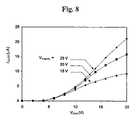
- FIG. 8shows input-output transfer characteristics for the 2-T pixel driver for different supply voltages
- FIG. 9shows input-output transfer characteristics for the 5-T pixel driver for different supply voltages
- FIG. 10shows variation in OLED current as a function of the normalized shift in threshold voltage
- FIG. 11shows a 2-T polysilicon based pixel current driver having p-channel drive TFTs
- FIG. 12shows a 4-T pixel current driver for OLED displays
- FIG. 13shows a 4-T pixel current driver with a lower discharge time
- FIG. 14shows a 4-T pixel current driver without non-linear gain
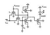
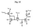
- FIG. 15shows a 4-T pixel current driver that is the building block for the full color circuit
- FIG. 16shows a full color(RGB) pixel current driver for OLED displays
- FIG. 17shows a schematic diagram of the top gate and the bottom gate of a dual gate transistor where the top gate is electrically connected to the bottom gate.
- amorphous Sidoes not enjoy equivalent electronic properties compared to poly-Si, it adequately meets many of the drive requirements for small area displays such as those needed in pagers, cell phones, and other mobile devices.
- Poly-Si TFTshave one key advantage in that they are able to provide better pixel drive capability because of their higher mobility, which can be of the order of ⁇ FE ⁇ 100 cm 2 /Vs. This makes poly-Si highly desirable for large area (e.g. laptop size) VGA and SVGA displays.
- the lower mobility associated with a-Si:H TFTs( ⁇ FE ⁇ 1 cm 2 /Vs) is not a limiting factor since the drive transistor in the pixel can be scaled up in area to provide the needed drive current.
- the OLED drive current densityis typically 10 mA/cm 2 at 10V operation to provide a brightness of 100 cd/m 2 —the required luminance for most displays.
- this drive current requirementtranslates into required pixel area of 300 ⁇ m 2 , which adequately meets the requirements of pixel resolution and speed for some 3 inch monochrome display applications.
- FIG. 1illustrates simulation results for the variation of the required pixel size with device mobility calculated for two types of drivers, which will be elaborated later, the 2-T and the 5-T drivers, wherein ⁇ 0 denotes a reference mobility whose value is in the range 0.1 to 1 cm 2 /Vs.
- the area of the pixel for the 2-T driver(see FIG. 5A ) comprises of the area of the switching transistors, area of the drive transistor, and the area occupied by interconnects, bias lines, etc.
- the drive current and frame rateare kept constant at 10 ⁇ A and 50 Hz, respectively, for a 230 ⁇ 230 array. It is clear that there is no significant savings in area between the 2-T and 5-T drivers but the savings are considerable with increasing mobility. This stems mainly from the reduction in the area of the drive transistor where there is a trade-off between ⁇ FE and TFT aspect ratio, W/L (Wide/Length).
- a-Si:HOne of the main advantages of the a-Si:H technology is that it has become low cost and well-established technology, while poly-Si has yet to reach the stage of manufacturability.
- the technologyalso holds great promise for futuristic applications since good as deposited a-Si:H, a-SiN x :H, and TFT arrays can be achieved at low temperatures ( ⁇ 120° C.) thus making it amenable to plastic substrates, which is a critical requirement for mechanically flexible displays.
- an alternate TFT structure based on a dual-gate structureis employed.
- a top gate electrodeis added to the TFT structure to prevent the OLED electrodes from biasing the a-Si:H channel area (refer to FIG. 2 ).
- the voltage on the top gatecan be chosen such so as to minimize the charge induced in the (parasitic) top channel of the TFT.
- the objective underlying the choice of the voltage on the top gateis to minimize parasitic capacitance in the driver circuits and leakage currents in the TFTs so as to enhance circuit performance.
- the operation of the dual-gate TFTis described, which will be central to surface emissive (100% aperture ratio) AMOLED displays based on a-Si:H backplane electronics.
- FIG. 3illustrates the structure of a dual-gate TFT fabricated for this purpose, wherein reference numerals S and D denote a source and a drain respectively.
- the fabrication stepsare the same as of that of a normal inverted staggered TFT structure except that it requires a sixth mask for patterning the top gate.
- the length of the TFTis around 30 ⁇ m to provide enough spacing between the source and drain for the top gate, and the width is made very large (1600 ⁇ m) with four of these TFTs are interconnected in parallel to create a sizeable leakage current for measurement.
- a delay timeis inserted in the measurement of the current to ensure that the measurement has passed the transient period created by defects in the a-Si:H active layer, which give rise to a time-dependent capacitance.
- FIG. 4shows results of static current measurements for four cases: first when the top gate is tied to ⁇ 10V, second when the top gate is grounded, third when the top gate is floating, and lastly when the top gate is shorted to the bottom gate.
- the leakage currentis relatively high particularly when the top gate is biased with a negative voltage.
- the lowest values of leakage currentare obtained when the top gate is pegged to either 0V or to the voltage of the bottom gate. In particular, with the latter the performance of the TFT in the (forward) sub-threshold regime of operation is significantly improved.
- top gate connectionbecomes extremely critical. For example, if the top gates in the pixel circuit are connected to the bottom gates of the associated TFTs, this gives rise to parasitic capacitances located between the gates and the cathode, which can lead to undesirable display operation (due to the charging up of the parasitic capacitance) when the multiplexer O/P drives the TFT switch. On the other hand, if the top gates are grounded, this results in the parasitic capacitance being grounded to yield reliable and stable circuit operation.
- the OLED drive circuits considered hereare the well-known voltage-programmed 2-T driver and the more sophisticated current-programmed ⁇ V T -compensated 5-T version (see FIGS. 5A and 6A ).
- the latteris a significant variation of the previous designs, leading to reduced pixel area ( ⁇ 300 ⁇ m), reduced leakage, lower supply voltage (20V), higher linearity ( ⁇ 30 db), and larger dynamic range ( ⁇ 40 dB).
- FIG. 5Bshows input-output timing diagrams of the 2-T pixel driver. When the address line is activated, the voltage on the data line starts charging capacitor C S and the gate capacitance of the driver transistor T 2 .
- the capacitorcharges up to turn the driver transistor T 2 on, which then starts conducting to drive the OLED with the appropriate level of current.
- T 1is turned off but the voltage at the gate of T 2 remains since the leakage current of T 1 is trivial in comparison. Hence, the current through the OLED remains unchanged after the turn off process.
- the OLED currentchanges only the next time around when a different voltage is written into the pixel.
- FIG. 6Bshows input-output timing diagrams of a 5-T pixel driver.
- the address line voltage, V address and I dataare activated or deactivated simultaneously.
- V addressWhen V address is activated, it forces T 1 and T 2 to turn on.
- T 1immediately starts conducting but T 2 does not since T 3 and T 4 are off. Therefore, the voltages at the drain and source of T 2 become equal.
- the current flow through T 1starts charging the gate capacitor of transistors T 3 and T 5 , very much like the 2-T driver. The current of these transistors start increasing and consequently T 2 starts to conduct current.
- T 1 's share of I datareduces and T 2 's share of I data increases. This process continues until the gate capacitors of T 3 and T 5 charge (via T 1 ) to a voltage that forces the current of T 3 to be I data . At this time, the current of T 1 is zero and the entire I data goes through T 2 and T 3 . At the same time, T 5 drives a current through the OLED, which is ideally equal to I data *(W 5 /W 3 ), which signifies a current gain.
- I data and V addressare deactivated, T 2 will turn off, but due to the presence of capacitances in T 3 and T 5 , the current of these two devices cannot be changed easily, since the capacitances keep the bias voltages constant. This forces T 4 to conduct the same current as that of T 3 , to enable the driver T 5 to drive the same current into the OLED even when the write period is over. Writing a new value into the pixel then changes the current driven into the OLED.
- the result of transient simulation for the 5-T driver circuitis shown in FIG. 7 .
- the circuithas a write time of ⁇ 70 ⁇ s, which is acceptable for most applications.
- the transfer characteristics for the 2-T and 5-T driver circuitsare illustrated in FIGS. 8 and 9 , respectively, generated using reliable physically-based TFT models for both forward and reverse regimes.
- FIG. 9a good dynamic range ( ⁇ 40 dB) is observed for supply voltage of 20V and drive currents in the range I OLED ⁇ 10 ⁇ A, which is realistic for high brightness.
- FIG. 10illustrates variation in the OLED current with the shift in threshold voltage for the 2-T and 5-T driver circuits.
- the 5-T driver circuitcompensates for the shift in threshold voltage particularly when the shift is smaller than 10% of the supply voltage. This is because the 5-T driver circuit is current-programmed. In contrast, the OLED current in the 2-T circuit changes significantly with a shift in threshold voltage.
- the 5-T driver circuit described hereoperates at much lower supply voltages, has a much larger drive current, and occupies less area.
- the pixel architecturesare compatible to surface (top) emissive AMOLED displays that enables high on-pixel TFT integration density for uniformity in OLED drive current and high aperture ratio.
- a 5-T driver circuithas been described that provides on-pixel gain, high linearity ( ⁇ 30 dB), and high dynamic range ( ⁇ 40 dB) at low supply voltages (15-20V) compared to the similar designs (27V).
- the results described hereillustrate the feasibility of using a-Si:H for 3-inch mobile monochrome display applications on both glass and plastic substrates. With the latter, although the mobility of the TFT is lower, the size of the drive transistor can be scaled up yet meeting the requirements on pixel area as depicted in FIG. 1 .
- Polysiliconhas higher electron and hole mobilities than amorphous silicon.
- the hole mobilitiesare large enough to allow the fabrication of p-channel TFTs.
- the advantage of having p-channel TFTsis that bottom emissive OLEDs can be used along with a p-channel drive TFT to make a very good current source.
- FIG. 11One such circuit is shown in FIG. 11 .
- the source of the p-type drive TFTis connected to Vdd. Therefore, Vgs, gate-to-source voltage, and hence the drive current of the p-type TFT is independent of OLED characteristics.
- the driver shown in FIG. 11performs as a good current source.
- bottom emissive OLEDsare suitable for use with p-channel drive TFTs
- top emissive OLEDsare suitable for use with n-channel TFTs.
- polysilicon TFTsrequire much higher temperatures than that of amorphous silicon. This high temperature processing requirement greatly increases the cost, and is not amenable to plastic substrates.
- polysilicon technologyis not as mature and widely available as amorphous silicon.
- amorphous siliconis a well-established technology currently used in liquid crystal displays (LCDs). It is due to these reasons that amorphous silicon combined with top emissive OLED based circuit designs is most promising for AMOLED displays.
- amorphous silicon TFTsare n-type and thus are more suitable for top emission circuits as shown in FIG. 2 .
- amorphous silicon TFTshave inherent stability problems due to the material structure.
- the biggest hurdleis the increase in threshold voltage V th after prolonged gate bias. This shift is particularly evident in the drive TFT of an OLED display pixel.
- This drive TFTis always in the ‘ON’ state, in which there is a positive voltage at its gate.
- the first current mirror based pixel driver circuitis presented, which automatically compensated for shifts in the V th of the drive TFT in a pixel.
- This circuitis the 5-T circuit shown in FIG. 6A .
- the first circuit shown in FIG. 12is a modification of the 5-T circuit of FIG. 6A .
- Transistor T 4has been removed from the 5-T circuit.
- This circuitoccupies a smaller area than the 5-T circuit, and provides a higher dynamic range.
- the higher dynamic rangeallows for a larger signal swing at the input, which means that the OLED brightness can be adjusted over a larger range.
- FIG. 12shows a 4-T pixel driver circuit for OLED displays.
- the circuit shown in FIG. 13is a 4-T pixel driver circuit based on a current mirror.
- the advantage of this circuitis that the discharge time of the capacitor Cs is substantially reduced. This is because the discharge path has two TFTs (as compared to three TFTs in the circuit of FIG. 12 ). The charging time remains the same.
- the other advantageis that there is an additional gain provided by this circuit because T 3 and T 4 do not have the same source voltages. However, this gain is non-linear and may not be desirable in some cases.
- FIG. 14another 4-T circuit is shown. This circuit does not have the non-linear gain present in the previous circuit ( FIG. 13 ) since the source terminals of T 3 and T 4 are at the same voltage. It still maintains the lower capacitance discharge time, along with the other features of the circuit of FIG. 8 .
- FIG. 15shows another version of the 4-T circuit. This circuit is does not have good current mirror properties. However, this circuit forms the building block for the 3 colour RGB circuit shown in FIG. 16 . It also has a low capacitance discharge time and high dynamic range.
- the full colour circuit shown in FIG. 16minimizes the area required by an RGB pixel on a display, while maintaining the desirable features like threshold voltage shift compensation, in-pixel current gain, low capacitance discharge time, and high dynamic range.
- the dual-gate TFTsare used in the above-mentioned circuits to enable vertical integration of the OLED layers with minimum parasitic effects. But nevertheless the circuit compensates for the Vth shift even if the simple single-gate TFTs. In addition, these circuits use n-type amorphous silicon TFTs. However, the circuits are applicable to polysilicon technology using p-type or n-type TFTs. These circuits when made in polysilicon can compensate for the non-uniformity of the threshold voltage, which is a problem in this technology.
- the p-type circuitsare conjugates of the above-mentioned circuits and are suitable for the bottom emissive pixels.
Landscapes
- Engineering & Computer Science (AREA)
- Physics & Mathematics (AREA)
- Computer Hardware Design (AREA)
- General Physics & Mathematics (AREA)
- Theoretical Computer Science (AREA)
- Microelectronics & Electronic Packaging (AREA)
- Electroluminescent Light Sources (AREA)
- Control Of Indicators Other Than Cathode Ray Tubes (AREA)
- Devices For Indicating Variable Information By Combining Individual Elements (AREA)
- Thin Film Transistor (AREA)
- Control Of El Displays (AREA)
Abstract
Description
Ids=(μCOXW/2L)(Vgs−Vth)2 (in Saturation region)
Claims (7)
Priority Applications (1)
| Application Number | Priority Date | Filing Date | Title |
|---|---|---|---|
| US11/247,455US7414600B2 (en) | 2001-02-16 | 2005-10-11 | Pixel current driver for organic light emitting diode displays |
Applications Claiming Priority (4)
| Application Number | Priority Date | Filing Date | Title |
|---|---|---|---|
| US26890001P | 2001-02-16 | 2001-02-16 | |
| PCT/CA2002/000173WO2002067327A2 (en) | 2001-02-16 | 2002-02-18 | Pixel current driver for organic light emitting diode displays |
| US10/468,319US20040129933A1 (en) | 2001-02-16 | 2002-02-18 | Pixel current driver for organic light emitting diode displays |
| US11/247,455US7414600B2 (en) | 2001-02-16 | 2005-10-11 | Pixel current driver for organic light emitting diode displays |
Related Parent Applications (3)
| Application Number | Title | Priority Date | Filing Date |
|---|---|---|---|
| US10/468,319ContinuationUS20040129933A1 (en) | 2001-02-16 | 2002-02-18 | Pixel current driver for organic light emitting diode displays |
| PCT/CA2002/000173ContinuationWO2002067327A2 (en) | 2001-02-16 | 2002-02-18 | Pixel current driver for organic light emitting diode displays |
| US10468319Continuation | 2002-02-18 |
Publications (2)
| Publication Number | Publication Date |
|---|---|
| US20060027807A1 US20060027807A1 (en) | 2006-02-09 |
| US7414600B2true US7414600B2 (en) | 2008-08-19 |
Family
ID=23024994
Family Applications (2)
| Application Number | Title | Priority Date | Filing Date |
|---|---|---|---|
| US10/468,319AbandonedUS20040129933A1 (en) | 2001-02-16 | 2002-02-18 | Pixel current driver for organic light emitting diode displays |
| US11/247,455Expired - LifetimeUS7414600B2 (en) | 2001-02-16 | 2005-10-11 | Pixel current driver for organic light emitting diode displays |
Family Applications Before (1)
| Application Number | Title | Priority Date | Filing Date |
|---|---|---|---|
| US10/468,319AbandonedUS20040129933A1 (en) | 2001-02-16 | 2002-02-18 | Pixel current driver for organic light emitting diode displays |
Country Status (4)
| Country | Link |
|---|---|
| US (2) | US20040129933A1 (en) |
| EP (2) | EP2180508A3 (en) |
| JP (1) | JP4383743B2 (en) |
| WO (1) | WO2002067327A2 (en) |
Cited By (114)
| Publication number | Priority date | Publication date | Assignee | Title |
|---|---|---|---|---|
| US20060103322A1 (en)* | 2004-11-17 | 2006-05-18 | Lg.Philips Lcd Co., Ltd. | Apparatus and method for driving organic light-emitting diode |
| US20070075638A1 (en)* | 2005-09-30 | 2007-04-05 | Casio Computer Co., Ltd | Display panel |
| US20080165096A1 (en)* | 2007-01-09 | 2008-07-10 | Himax Technologies Limited | Flat Panel Display |
| US20090022624A1 (en)* | 2003-01-14 | 2009-01-22 | Micronics, Inc. | Microfluidic devices for fluid manipulation and analysis |
| US20090244057A1 (en)* | 2008-03-26 | 2009-10-01 | Fujifilm Corporation | Pixel circuit and display apparatus |
| US20090244046A1 (en)* | 2008-03-26 | 2009-10-01 | Fujifilm Corporation | Pixel circuit, display apparatus, and pixel circuit drive control method |
| US20100033469A1 (en)* | 2004-12-15 | 2010-02-11 | Ignis Innovation Inc. | Method and system for programming, calibrating and driving a light emitting device display |
| US20100225657A1 (en)* | 2009-03-06 | 2010-09-09 | Sakariya Kapil V | Systems and methods for operating a display |
| US20100225571A1 (en)* | 2009-03-06 | 2010-09-09 | Sakariya Kapil V | Circuitry for independent gamma adjustment points |
| US20100328299A1 (en)* | 2001-09-21 | 2010-12-30 | Semiconductor Energy Laboratory Co., Ltd. | Light emitting device, driving method of light emitting device and electronic device |
| US20110080442A1 (en)* | 2009-10-05 | 2011-04-07 | Emagin Corporation | system for color shift compensation in an oled display using a look-up table, a method and a computer-readable medium |
| US20110084281A1 (en)* | 2001-02-26 | 2011-04-14 | Semiconductor Energy Laboratory Co., Ltd. | Light emitting device and electronic equipment |
| US20120162275A1 (en)* | 2010-12-28 | 2012-06-28 | Samsung Mobile Display Co., Ltd. | Organic light emitting display device, driving method thereof, and manufacturing method thereof |
| US8553024B2 (en) | 2010-12-30 | 2013-10-08 | Au Optronics Corp. | Pixel driving circuit of an organic light emitting diode |
| US8564513B2 (en) | 2006-01-09 | 2013-10-22 | Ignis Innovation, Inc. | Method and system for driving an active matrix display circuit |
| US8599191B2 (en) | 2011-05-20 | 2013-12-03 | Ignis Innovation Inc. | System and methods for extraction of threshold and mobility parameters in AMOLED displays |
| US8692743B2 (en) | 2010-10-28 | 2014-04-08 | Au Optronics Corp. | Pixel driving circuit of an organic light emitting diode |
| US8743096B2 (en) | 2006-04-19 | 2014-06-03 | Ignis Innovation, Inc. | Stable driving scheme for active matrix displays |
| US8803417B2 (en) | 2009-12-01 | 2014-08-12 | Ignis Innovation Inc. | High resolution pixel architecture |
| US8847942B2 (en) | 2011-03-29 | 2014-09-30 | Intrigue Technologies, Inc. | Method and circuit for compensating pixel drift in active matrix displays |
| US8860636B2 (en) | 2005-06-08 | 2014-10-14 | Ignis Innovation Inc. | Method and system for driving a light emitting device display |
| US8890220B2 (en) | 2001-02-16 | 2014-11-18 | Ignis Innovation, Inc. | Pixel driver circuit and pixel circuit having control circuit coupled to supply voltage |
| US8907991B2 (en) | 2010-12-02 | 2014-12-09 | Ignis Innovation Inc. | System and methods for thermal compensation in AMOLED displays |
| USRE45291E1 (en) | 2004-06-29 | 2014-12-16 | Ignis Innovation Inc. | Voltage-programming scheme for current-driven AMOLED displays |
| US8922544B2 (en) | 2012-05-23 | 2014-12-30 | Ignis Innovation Inc. | Display systems with compensation for line propagation delay |
| US8941697B2 (en) | 2003-09-23 | 2015-01-27 | Ignis Innovation Inc. | Circuit and method for driving an array of light emitting pixels |
| US8994617B2 (en) | 2010-03-17 | 2015-03-31 | Ignis Innovation Inc. | Lifetime uniformity parameter extraction methods |
| US9030506B2 (en) | 2009-11-12 | 2015-05-12 | Ignis Innovation Inc. | Stable fast programming scheme for displays |
| US20150179635A1 (en)* | 2011-09-16 | 2015-06-25 | Semiconductor Energy Laboratory Co., Ltd. | Semiconductor device, light-emitting device, and electronic device |
| US9070775B2 (en) | 2011-08-03 | 2015-06-30 | Ignis Innovations Inc. | Thin film transistor |
| US9093028B2 (en) | 2009-12-06 | 2015-07-28 | Ignis Innovation Inc. | System and methods for power conservation for AMOLED pixel drivers |
| US9093029B2 (en) | 2011-05-20 | 2015-07-28 | Ignis Innovation Inc. | System and methods for extraction of threshold and mobility parameters in AMOLED displays |
| US9111485B2 (en) | 2009-06-16 | 2015-08-18 | Ignis Innovation Inc. | Compensation technique for color shift in displays |
| US9125278B2 (en) | 2006-08-15 | 2015-09-01 | Ignis Innovation Inc. | OLED luminance degradation compensation |
| US9134825B2 (en) | 2011-05-17 | 2015-09-15 | Ignis Innovation Inc. | Systems and methods for display systems with dynamic power control |
| US20150270408A1 (en)* | 2014-03-18 | 2015-09-24 | Samsung Display Co., Ltd. | Thin film transistor array panel and manufacturing method thereof |
| US9153172B2 (en) | 2004-12-07 | 2015-10-06 | Ignis Innovation Inc. | Method and system for programming and driving active matrix light emitting device pixel having a controllable supply voltage |
| US9171504B2 (en) | 2013-01-14 | 2015-10-27 | Ignis Innovation Inc. | Driving scheme for emissive displays providing compensation for driving transistor variations |
| US9171500B2 (en) | 2011-05-20 | 2015-10-27 | Ignis Innovation Inc. | System and methods for extraction of parasitic parameters in AMOLED displays |
| US9224954B2 (en) | 2011-08-03 | 2015-12-29 | Ignis Innovation Inc. | Organic light emitting diode and method of manufacturing |
| US20160035807A1 (en)* | 2013-09-27 | 2016-02-04 | Boe Technology Group Co., Ltd. | Oled pixel structure and oled display device |
| US9269322B2 (en) | 2006-01-09 | 2016-02-23 | Ignis Innovation Inc. | Method and system for driving an active matrix display circuit |
| US9275579B2 (en) | 2004-12-15 | 2016-03-01 | Ignis Innovation Inc. | System and methods for extraction of threshold and mobility parameters in AMOLED displays |
| US9280933B2 (en) | 2004-12-15 | 2016-03-08 | Ignis Innovation Inc. | System and methods for extraction of threshold and mobility parameters in AMOLED displays |
| US9305488B2 (en) | 2013-03-14 | 2016-04-05 | Ignis Innovation Inc. | Re-interpolation with edge detection for extracting an aging pattern for AMOLED displays |
| US9311859B2 (en) | 2009-11-30 | 2016-04-12 | Ignis Innovation Inc. | Resetting cycle for aging compensation in AMOLED displays |
| US9324268B2 (en) | 2013-03-15 | 2016-04-26 | Ignis Innovation Inc. | Amoled displays with multiple readout circuits |
| US9336717B2 (en) | 2012-12-11 | 2016-05-10 | Ignis Innovation Inc. | Pixel circuits for AMOLED displays |
| US9343006B2 (en) | 2012-02-03 | 2016-05-17 | Ignis Innovation Inc. | Driving system for active-matrix displays |
| US9351368B2 (en) | 2013-03-08 | 2016-05-24 | Ignis Innovation Inc. | Pixel circuits for AMOLED displays |
| US9370075B2 (en) | 2008-12-09 | 2016-06-14 | Ignis Innovation Inc. | System and method for fast compensation programming of pixels in a display |
| US9373645B2 (en) | 2005-01-28 | 2016-06-21 | Ignis Innovation Inc. | Voltage programmed pixel circuit, display system and driving method thereof |
| US9385169B2 (en) | 2011-11-29 | 2016-07-05 | Ignis Innovation Inc. | Multi-functional active matrix organic light-emitting diode display |
| US9384698B2 (en) | 2009-11-30 | 2016-07-05 | Ignis Innovation Inc. | System and methods for aging compensation in AMOLED displays |
| US9430958B2 (en) | 2010-02-04 | 2016-08-30 | Ignis Innovation Inc. | System and methods for extracting correlation curves for an organic light emitting device |
| US9437137B2 (en) | 2013-08-12 | 2016-09-06 | Ignis Innovation Inc. | Compensation accuracy |
| US9466240B2 (en) | 2011-05-26 | 2016-10-11 | Ignis Innovation Inc. | Adaptive feedback system for compensating for aging pixel areas with enhanced estimation speed |
| US9489891B2 (en) | 2006-01-09 | 2016-11-08 | Ignis Innovation Inc. | Method and system for driving an active matrix display circuit |
| US9502653B2 (en) | 2013-12-25 | 2016-11-22 | Ignis Innovation Inc. | Electrode contacts |
| US9530349B2 (en) | 2011-05-20 | 2016-12-27 | Ignis Innovations Inc. | Charged-based compensation and parameter extraction in AMOLED displays |
| US9606607B2 (en) | 2011-05-17 | 2017-03-28 | Ignis Innovation Inc. | Systems and methods for display systems with dynamic power control |
| US9697771B2 (en) | 2013-03-08 | 2017-07-04 | Ignis Innovation Inc. | Pixel circuits for AMOLED displays |
| US9721505B2 (en) | 2013-03-08 | 2017-08-01 | Ignis Innovation Inc. | Pixel circuits for AMOLED displays |
| US9741282B2 (en) | 2013-12-06 | 2017-08-22 | Ignis Innovation Inc. | OLED display system and method |
| US9747834B2 (en) | 2012-05-11 | 2017-08-29 | Ignis Innovation Inc. | Pixel circuits including feedback capacitors and reset capacitors, and display systems therefore |
| US9761170B2 (en) | 2013-12-06 | 2017-09-12 | Ignis Innovation Inc. | Correction for localized phenomena in an image array |
| USRE46561E1 (en) | 2008-07-29 | 2017-09-26 | Ignis Innovation Inc. | Method and system for driving light emitting display |
| US9773439B2 (en) | 2011-05-27 | 2017-09-26 | Ignis Innovation Inc. | Systems and methods for aging compensation in AMOLED displays |
| US9786209B2 (en) | 2009-11-30 | 2017-10-10 | Ignis Innovation Inc. | System and methods for aging compensation in AMOLED displays |
| US9786223B2 (en) | 2012-12-11 | 2017-10-10 | Ignis Innovation Inc. | Pixel circuits for AMOLED displays |
| US9799246B2 (en) | 2011-05-20 | 2017-10-24 | Ignis Innovation Inc. | System and methods for extraction of threshold and mobility parameters in AMOLED displays |
| US9806197B1 (en) | 2016-07-13 | 2017-10-31 | Innolux Corporation | Display device having back gate electrodes |
| US9830857B2 (en) | 2013-01-14 | 2017-11-28 | Ignis Innovation Inc. | Cleaning common unwanted signals from pixel measurements in emissive displays |
| US9842889B2 (en) | 2014-11-28 | 2017-12-12 | Ignis Innovation Inc. | High pixel density array architecture |
| US9867257B2 (en) | 2008-04-18 | 2018-01-09 | Ignis Innovation Inc. | System and driving method for light emitting device display |
| US9881532B2 (en) | 2010-02-04 | 2018-01-30 | Ignis Innovation Inc. | System and method for extracting correlation curves for an organic light emitting device |
| US9881587B2 (en) | 2011-05-28 | 2018-01-30 | Ignis Innovation Inc. | Systems and methods for operating pixels in a display to mitigate image flicker |
| US9886899B2 (en) | 2011-05-17 | 2018-02-06 | Ignis Innovation Inc. | Pixel Circuits for AMOLED displays |
| US9947293B2 (en) | 2015-05-27 | 2018-04-17 | Ignis Innovation Inc. | Systems and methods of reduced memory bandwidth compensation |
| US9952698B2 (en) | 2013-03-15 | 2018-04-24 | Ignis Innovation Inc. | Dynamic adjustment of touch resolutions on an AMOLED display |
| US10013907B2 (en) | 2004-12-15 | 2018-07-03 | Ignis Innovation Inc. | Method and system for programming, calibrating and/or compensating, and driving an LED display |
| US10012678B2 (en) | 2004-12-15 | 2018-07-03 | Ignis Innovation Inc. | Method and system for programming, calibrating and/or compensating, and driving an LED display |
| US10019941B2 (en) | 2005-09-13 | 2018-07-10 | Ignis Innovation Inc. | Compensation technique for luminance degradation in electro-luminance devices |
| US10074304B2 (en) | 2015-08-07 | 2018-09-11 | Ignis Innovation Inc. | Systems and methods of pixel calibration based on improved reference values |
| US10078984B2 (en) | 2005-02-10 | 2018-09-18 | Ignis Innovation Inc. | Driving circuit for current programmed organic light-emitting diode displays |
| US10089924B2 (en) | 2011-11-29 | 2018-10-02 | Ignis Innovation Inc. | Structural and low-frequency non-uniformity compensation |
| US10089921B2 (en) | 2010-02-04 | 2018-10-02 | Ignis Innovation Inc. | System and methods for extracting correlation curves for an organic light emitting device |
| US10102808B2 (en) | 2015-10-14 | 2018-10-16 | Ignis Innovation Inc. | Systems and methods of multiple color driving |
| US10134325B2 (en) | 2014-12-08 | 2018-11-20 | Ignis Innovation Inc. | Integrated display system |
| US10152915B2 (en) | 2015-04-01 | 2018-12-11 | Ignis Innovation Inc. | Systems and methods of display brightness adjustment |
| US10163401B2 (en) | 2010-02-04 | 2018-12-25 | Ignis Innovation Inc. | System and methods for extracting correlation curves for an organic light emitting device |
| US10163996B2 (en) | 2003-02-24 | 2018-12-25 | Ignis Innovation Inc. | Pixel having an organic light emitting diode and method of fabricating the pixel |
| US10176752B2 (en) | 2014-03-24 | 2019-01-08 | Ignis Innovation Inc. | Integrated gate driver |
| US10176736B2 (en) | 2010-02-04 | 2019-01-08 | Ignis Innovation Inc. | System and methods for extracting correlation curves for an organic light emitting device |
| US10181282B2 (en) | 2015-01-23 | 2019-01-15 | Ignis Innovation Inc. | Compensation for color variations in emissive devices |
| US10192479B2 (en) | 2014-04-08 | 2019-01-29 | Ignis Innovation Inc. | Display system using system level resources to calculate compensation parameters for a display module in a portable device |
| US10204540B2 (en) | 2015-10-26 | 2019-02-12 | Ignis Innovation Inc. | High density pixel pattern |
| US10235933B2 (en) | 2005-04-12 | 2019-03-19 | Ignis Innovation Inc. | System and method for compensation of non-uniformities in light emitting device displays |
| US10242619B2 (en) | 2013-03-08 | 2019-03-26 | Ignis Innovation Inc. | Pixel circuits for amoled displays |
| US10311780B2 (en) | 2015-05-04 | 2019-06-04 | Ignis Innovation Inc. | Systems and methods of optical feedback |
| US10319307B2 (en) | 2009-06-16 | 2019-06-11 | Ignis Innovation Inc. | Display system with compensation techniques and/or shared level resources |
| US10373554B2 (en) | 2015-07-24 | 2019-08-06 | Ignis Innovation Inc. | Pixels and reference circuits and timing techniques |
| US10410579B2 (en) | 2015-07-24 | 2019-09-10 | Ignis Innovation Inc. | Systems and methods of hybrid calibration of bias current |
| US10573231B2 (en) | 2010-02-04 | 2020-02-25 | Ignis Innovation Inc. | System and methods for extracting correlation curves for an organic light emitting device |
| US10586491B2 (en) | 2016-12-06 | 2020-03-10 | Ignis Innovation Inc. | Pixel circuits for mitigation of hysteresis |
| US10657895B2 (en) | 2015-07-24 | 2020-05-19 | Ignis Innovation Inc. | Pixels and reference circuits and timing techniques |
| TWI697884B (en)* | 2019-08-20 | 2020-07-01 | 友達光電股份有限公司 | Pixel circuit |
| US10714018B2 (en) | 2017-05-17 | 2020-07-14 | Ignis Innovation Inc. | System and method for loading image correction data for displays |
| US10783818B2 (en) | 2018-07-24 | 2020-09-22 | Au Optronics Corporation | Dual gate transistor circuit, pixel circuit and gate drive circuit thereof |
| US10867536B2 (en) | 2013-04-22 | 2020-12-15 | Ignis Innovation Inc. | Inspection system for OLED display panels |
| US10971078B2 (en) | 2018-02-12 | 2021-04-06 | Ignis Innovation Inc. | Pixel measurement through data line |
| US10996258B2 (en) | 2009-11-30 | 2021-05-04 | Ignis Innovation Inc. | Defect detection and correction of pixel circuits for AMOLED displays |
| US10997901B2 (en) | 2014-02-28 | 2021-05-04 | Ignis Innovation Inc. | Display system |
| US11025899B2 (en) | 2017-08-11 | 2021-06-01 | Ignis Innovation Inc. | Optical correction systems and methods for correcting non-uniformity of emissive display devices |
Families Citing this family (45)
| Publication number | Priority date | Publication date | Assignee | Title |
|---|---|---|---|---|
| US6753654B2 (en)* | 2001-02-21 | 2004-06-22 | Semiconductor Energy Laboratory Co., Ltd. | Light emitting device and electronic appliance |
| JP4212815B2 (en)* | 2001-02-21 | 2009-01-21 | 株式会社半導体エネルギー研究所 | Light emitting device |
| US6777249B2 (en)* | 2001-06-01 | 2004-08-17 | Semiconductor Energy Laboratory Co., Ltd. | Method of repairing a light-emitting device, and method of manufacturing a light-emitting device |
| JP2010122700A (en)* | 2001-09-10 | 2010-06-03 | Seiko Epson Corp | Electro-optical device and electronic equipment |
| JP4742726B2 (en)* | 2001-09-10 | 2011-08-10 | セイコーエプソン株式会社 | Electronic device and electronic device |
| JP4581893B2 (en)* | 2001-09-10 | 2010-11-17 | セイコーエプソン株式会社 | Electronic device and electronic device |
| TW588468B (en)* | 2002-09-19 | 2004-05-21 | Ind Tech Res Inst | Pixel structure of active matrix organic light-emitting diode |
| JP4373331B2 (en)* | 2002-11-27 | 2009-11-25 | 株式会社半導体エネルギー研究所 | Display device |
| JP4494214B2 (en)* | 2002-11-29 | 2010-06-30 | 株式会社半導体エネルギー研究所 | Display device, electronic equipment |
| US6975293B2 (en)* | 2003-01-31 | 2005-12-13 | Faraday Technology Corp. | Active matrix LED display driving circuit |
| TWI228696B (en)* | 2003-03-21 | 2005-03-01 | Ind Tech Res Inst | Pixel circuit for active matrix OLED and driving method |
| TW200428688A (en)* | 2003-06-05 | 2004-12-16 | Au Optronics Corp | Organic light-emitting display and its pixel structure |
| TWI220100B (en)* | 2003-06-05 | 2004-08-01 | Au Optronics Corp | OLED display and pixel structure thereof |
| US7532187B2 (en)* | 2004-09-28 | 2009-05-12 | Sharp Laboratories Of America, Inc. | Dual-gate transistor display |
| JP5152448B2 (en)* | 2004-09-21 | 2013-02-27 | カシオ計算機株式会社 | Pixel drive circuit and image display device |
| EP1825455A4 (en)* | 2004-11-16 | 2009-05-06 | Ignis Innovation Inc | System and driving method for active matrix light emitting device display |
| CA2490861A1 (en)* | 2004-12-01 | 2006-06-01 | Ignis Innovation Inc. | Fuzzy control for stable amoled displays |
| US7317434B2 (en)* | 2004-12-03 | 2008-01-08 | Dupont Displays, Inc. | Circuits including switches for electronic devices and methods of using the electronic devices |
| US20060118869A1 (en)* | 2004-12-03 | 2006-06-08 | Je-Hsiung Lan | Thin-film transistors and processes for forming the same |
| US20070090459A1 (en)* | 2005-10-26 | 2007-04-26 | Motorola, Inc. | Multiple gate printed transistor method and apparatus |
| US8232931B2 (en)* | 2006-04-10 | 2012-07-31 | Emagin Corporation | Auto-calibrating gamma correction circuit for AMOLED pixel display driver |
| JP4748456B2 (en)* | 2006-09-26 | 2011-08-17 | カシオ計算機株式会社 | Pixel drive circuit and image display device |
| JP5207885B2 (en) | 2008-09-03 | 2013-06-12 | キヤノン株式会社 | Pixel circuit, light emitting display device and driving method thereof |
| JP5663214B2 (en)* | 2009-07-03 | 2015-02-04 | 株式会社半導体エネルギー研究所 | Method for manufacturing semiconductor device |
| WO2011065258A1 (en)* | 2009-11-27 | 2011-06-03 | Semiconductor Energy Laboratory Co., Ltd. | Semiconductor device |
| KR101117729B1 (en)* | 2009-12-17 | 2012-03-07 | 삼성모바일디스플레이주식회사 | Pixel circuit, and organic light emitting display and method for controlling a brightness thereof |
| CN102917734B (en)* | 2010-06-02 | 2014-12-17 | 三菱电机株式会社 | Device and method for microbe and virus capture and inactivation |
| JP5178861B2 (en)* | 2011-03-01 | 2013-04-10 | 株式会社半導体エネルギー研究所 | Display device |
| CN103117042B (en)* | 2013-02-22 | 2015-03-18 | 合肥京东方光电科技有限公司 | Pixel unit drive circuit, pixel unit drive method, pixel unit and display device |
| US9754971B2 (en) | 2013-05-18 | 2017-09-05 | Semiconductor Energy Laboratory Co., Ltd. | Semiconductor device |
| KR102241704B1 (en)* | 2014-08-07 | 2021-04-20 | 삼성디스플레이 주식회사 | Pixel circuit and organic light emitting display device having the same |
| CN104269429B (en)* | 2014-09-19 | 2017-05-31 | 京东方科技集团股份有限公司 | A kind of organic elctroluminescent device, its driving method and display device |
| KR102295221B1 (en)* | 2014-12-26 | 2021-09-01 | 삼성디스플레이 주식회사 | Gate driving circuit and display device having the same |
| CN105932032A (en) | 2016-06-16 | 2016-09-07 | 深圳市华星光电技术有限公司 | Array substrate and preparation method therefor |
| JP2018036290A (en)* | 2016-08-29 | 2018-03-08 | 株式会社ジャパンディスプレイ | Display device |
| US10839771B2 (en) | 2016-12-22 | 2020-11-17 | Intel Corporation | Display driver |
| US10909933B2 (en) | 2016-12-22 | 2021-02-02 | Intel Corporation | Digital driver for displays |
| US20180182295A1 (en)* | 2016-12-22 | 2018-06-28 | Intel Corporation | Current programmed pixel architecture for displays |
| CN106558287B (en)* | 2017-01-25 | 2019-05-07 | 上海天马有机发光显示技术有限公司 | Organic light-emitting pixel driving circuit, driving method and organic light-emitting display panel |
| EP3367374A1 (en) | 2017-02-28 | 2018-08-29 | IMEC vzw | An active matrix display and a method for threshold voltage compensation in an active matrix display |
| US10565935B2 (en) | 2017-09-04 | 2020-02-18 | Shenzhen China Star Optoelectronics Semiconductor Display Technology Co., Ltd | Scan driving circuit for OLED and display panel |
| JP7116539B2 (en)* | 2017-11-27 | 2022-08-10 | 株式会社ジャパンディスプレイ | Display device |
| TWI685832B (en)* | 2019-01-15 | 2020-02-21 | 友達光電股份有限公司 | Pixel driving circuit and the operating method thereof |
| KR102780541B1 (en)* | 2019-09-24 | 2025-03-12 | 삼성디스플레이 주식회사 | Pixel circuit and display device including the same |
| EP4016517A1 (en)* | 2020-12-18 | 2022-06-22 | Imec VZW | Compensated current mirror circuit |
Citations (34)
| Publication number | Priority date | Publication date | Assignee | Title |
|---|---|---|---|---|
| US4996523A (en) | 1988-10-20 | 1991-02-26 | Eastman Kodak Company | Electroluminescent storage display with improved intensity driver circuits |
| US5266515A (en) | 1992-03-02 | 1993-11-30 | Motorola, Inc. | Fabricating dual gate thin film transistors |
| US5498880A (en) | 1995-01-12 | 1996-03-12 | E. I. Du Pont De Nemours And Company | Image capture panel using a solid state device |
| JPH0990405A (en) | 1995-09-21 | 1997-04-04 | Sharp Corp | Thin film transistor |
| US5619033A (en) | 1995-06-07 | 1997-04-08 | Xerox Corporation | Layered solid state photodiode sensor array |
| US5648276A (en) | 1993-05-27 | 1997-07-15 | Sony Corporation | Method and apparatus for fabricating a thin film semiconductor device |
| US5714968A (en) | 1994-08-09 | 1998-02-03 | Nec Corporation | Current-dependent light-emitting element drive circuit for use in active matrix display device |
| US5874803A (en) | 1997-09-09 | 1999-02-23 | The Trustees Of Princeton University | Light emitting device with stack of OLEDS and phosphor downconverter |
| US5903248A (en) | 1997-04-11 | 1999-05-11 | Spatialight, Inc. | Active matrix display having pixel driving circuits with integrated charge pumps |
| US5917280A (en) | 1997-02-03 | 1999-06-29 | The Trustees Of Princeton University | Stacked organic light emitting devices |
| JPH11231805A (en) | 1998-02-10 | 1999-08-27 | Sanyo Electric Co Ltd | Display device |
| US6023259A (en) | 1997-07-11 | 2000-02-08 | Fed Corporation | OLED active matrix using a single transistor current mode pixel design |
| CA2242720C (en) | 1998-07-09 | 2000-05-16 | Ibm Canada Limited-Ibm Canada Limitee | Programmable led driver |
| US6091203A (en) | 1998-03-31 | 2000-07-18 | Nec Corporation | Image display device with element driving device for matrix drive of multiple active elements |
| EP1028471A2 (en) | 1999-02-09 | 2000-08-16 | SANYO ELECTRIC Co., Ltd. | Electroluminescence display device |
| US6229508B1 (en) | 1997-09-29 | 2001-05-08 | Sarnoff Corporation | Active matrix light emitting diode pixel structure and concomitant method |
| US20010002703A1 (en) | 1999-11-30 | 2001-06-07 | Jun Koyama | Electric device |
| US6246180B1 (en) | 1999-01-29 | 2001-06-12 | Nec Corporation | Organic el display device having an improved image quality |
| US6252248B1 (en) | 1998-06-08 | 2001-06-26 | Sanyo Electric Co., Ltd. | Thin film transistor and display |
| EP1130565A1 (en) | 1999-07-14 | 2001-09-05 | Sony Corporation | Current drive circuit and display comprising the same, pixel circuit, and drive method |
| US20010026257A1 (en) | 2000-03-27 | 2001-10-04 | Hajime Kimura | Electro-optical device |
| US20010030323A1 (en) | 2000-03-29 | 2001-10-18 | Sony Corporation | Thin film semiconductor apparatus and method for driving the same |
| US6307322B1 (en) | 1999-12-28 | 2001-10-23 | Sarnoff Corporation | Thin-film transistor circuitry with reduced sensitivity to variance in transistor threshold voltage |
| US20010043173A1 (en) | 1997-09-04 | 2001-11-22 | Ronald Roy Troutman | Field sequential gray in active matrix led display using complementary transistor pixel circuits |
| US20010045929A1 (en) | 2000-01-21 | 2001-11-29 | Prache Olivier F. | Gray scale pixel driver for electronic display and method of operation therefor |
| US20020000576A1 (en) | 2000-06-22 | 2002-01-03 | Kazutaka Inukai | Display device |
| US20020011796A1 (en) | 2000-05-08 | 2002-01-31 | Semiconductor Energy Laboratory Co., Ltd. | Light-emitting device, and electric device using the same |
| US20020011799A1 (en) | 2000-04-06 | 2002-01-31 | Semiconductor Energy Laboratory Co., Ltd. | Electronic device and driving method |
| US6580408B1 (en) | 1999-06-03 | 2003-06-17 | Lg. Philips Lcd Co., Ltd. | Electro-luminescent display including a current mirror |
| US6693610B2 (en)* | 1999-09-11 | 2004-02-17 | Koninklijke Philips Electronics N.V. | Active matrix electroluminescent display device |
| US20050067971A1 (en)* | 2003-09-29 | 2005-03-31 | Michael Gillis Kane | Pixel circuit for an active matrix organic light-emitting diode display |
| US7129914B2 (en)* | 2001-12-20 | 2006-10-31 | Koninklijke Philips Electronics N. V. | Active matrix electroluminescent display device |
| US20060261841A1 (en)* | 2004-08-20 | 2006-11-23 | Koninklijke Philips Electronics N.V. | Data signal driver for light emitting display |
| US7248236B2 (en)* | 2001-02-16 | 2007-07-24 | Ignis Innovation Inc. | Organic light emitting diode display having shield electrodes |
Family Cites Families (36)
| Publication number | Priority date | Publication date | Assignee | Title |
|---|---|---|---|---|
| US1585976A (en)* | 1922-03-02 | 1926-05-25 | Stemco Engineering Company | Fluid gauge |
| US1544838A (en)* | 1923-08-25 | 1925-07-07 | Electric Water Sterilizer & Oz | Ozone generator |
| US1743202A (en)* | 1926-10-04 | 1930-01-14 | Sun Maid Raisin Growers Of Cal | Ozone apparatus |
| US2113913A (en)* | 1936-02-01 | 1938-04-12 | Wilson H Cragun | Ozonator |
| US3607709A (en)* | 1969-03-13 | 1971-09-21 | Air And Water Purification Inc | Ozone generator |
| US3784838A (en)* | 1971-08-25 | 1974-01-08 | Purification Sciences Inc | Solid state frequency converter for corona generator |
| US3801791A (en)* | 1971-11-15 | 1974-04-02 | R Schaefer | Ozone generator |
| US3883413A (en)* | 1972-09-25 | 1975-05-13 | Avco Corp | Ozone generator using pulsed electron beam and decaying electric field |
| DE2539715C3 (en)* | 1975-09-06 | 1978-06-22 | Pavel Dr. 3257 Springe Imris | Device for the production of ozone |
| US4159971A (en)* | 1976-02-19 | 1979-07-03 | Arthur Gneupel | Ozone generator |
| US4386395A (en)* | 1980-12-19 | 1983-05-31 | Webster Electric Company, Inc. | Power supply for electrostatic apparatus |
| DE3247374A1 (en)* | 1982-12-22 | 1984-07-05 | Bruno Bachhofer | OZONE GENERATOR WITH HIGH-VOLTAGE PLATE-SHAPED ELECTRODES |
| US4970056A (en)* | 1989-01-18 | 1990-11-13 | Fusion Systems Corporation | Ozone generator with improved dielectric and method of manufacture |
| US5047744A (en)* | 1990-01-23 | 1991-09-10 | Plasma Technics, Inc. | High voltage fluid filled transformer |
| US5137697A (en)* | 1991-05-23 | 1992-08-11 | Quantum Electronics Corporation | Ozone generator |
| US5124132A (en)* | 1991-06-20 | 1992-06-23 | Plasma Technics, Inc. | Corona discharge ozone generator |
| US5258165A (en)* | 1991-06-26 | 1993-11-02 | Osmonics, Inc. | Multi-tube ozone generator and method of making same |
| JP2776083B2 (en)* | 1991-08-23 | 1998-07-16 | 日本電気株式会社 | Liquid crystal display device and manufacturing method thereof |
| US5417936A (en)* | 1992-06-08 | 1995-05-23 | Nippon Ozone Co., Ltd. | Plate-type ozone generator |
| CA2075789C (en)* | 1992-08-11 | 1998-12-22 | Amir Salama | Inner electrode for an ozone generator, ozone generator containing said electrode and method of use of said ozone generator |
| US5313145A (en)* | 1992-08-31 | 1994-05-17 | Francis Jr Ralph M | Power supply for a gas discharge device |
| US5554345A (en)* | 1992-10-14 | 1996-09-10 | Novozone (N.V.) Limited | Ozone generation apparatus and method |
| US5503809A (en)* | 1993-04-19 | 1996-04-02 | John T. Towles | Compact ozone generator |
| US5424893A (en)* | 1994-03-11 | 1995-06-13 | Francis, Jr.; Ralph M. | Gas discharge device power supply with ground fault protection |
| US5637279A (en)* | 1994-08-31 | 1997-06-10 | Applied Science & Technology, Inc. | Ozone and other reactive gas generator cell and system |
| GB2309875B (en)* | 1996-02-02 | 2000-12-20 | Ozone Ind Ltd | An ozone generator |
| US5788930A (en)* | 1996-08-21 | 1998-08-04 | Mcmurray; Larry Daniel | Apparatus for purifying an environment using ozone generation |
| US5803982A (en)* | 1996-10-15 | 1998-09-08 | Ez Environmental Solutions Corporation | Pressure washing apparatus with ozone generator |
| US5911957A (en)* | 1997-10-23 | 1999-06-15 | Khatchatrian; Robert G. | Ozone generator |
| JP2953465B1 (en)* | 1998-08-14 | 1999-09-27 | 日本電気株式会社 | Constant current drive circuit |
| JP4337171B2 (en)* | 1999-06-14 | 2009-09-30 | ソニー株式会社 | Display device |
| JP3548063B2 (en)* | 1999-10-20 | 2004-07-28 | 三洋電機株式会社 | Active matrix display |
| JP3594126B2 (en)* | 2000-10-13 | 2004-11-24 | 日本電気株式会社 | Current drive circuit |
| JP4212815B2 (en)* | 2001-02-21 | 2009-01-21 | 株式会社半導体エネルギー研究所 | Light emitting device |
| JP4075505B2 (en)* | 2001-09-10 | 2008-04-16 | セイコーエプソン株式会社 | Electronic circuit, electronic device, and electronic apparatus |
| SG120889A1 (en)* | 2001-09-28 | 2006-04-26 | Semiconductor Energy Lab | A light emitting device and electronic apparatus using the same |
- 2002
- 2002-02-18USUS10/468,319patent/US20040129933A1/ennot_activeAbandoned
- 2002-02-18EPEP10000421Apatent/EP2180508A3/ennot_activeWithdrawn
- 2002-02-18WOPCT/CA2002/000173patent/WO2002067327A2/enactiveApplication Filing
- 2002-02-18EPEP02711721Apatent/EP1488454B1/ennot_activeExpired - Lifetime
- 2002-02-18JPJP2002566552Apatent/JP4383743B2/ennot_activeExpired - Lifetime
- 2005
- 2005-10-11USUS11/247,455patent/US7414600B2/ennot_activeExpired - Lifetime
Patent Citations (34)
| Publication number | Priority date | Publication date | Assignee | Title |
|---|---|---|---|---|
| US4996523A (en) | 1988-10-20 | 1991-02-26 | Eastman Kodak Company | Electroluminescent storage display with improved intensity driver circuits |
| US5266515A (en) | 1992-03-02 | 1993-11-30 | Motorola, Inc. | Fabricating dual gate thin film transistors |
| US5648276A (en) | 1993-05-27 | 1997-07-15 | Sony Corporation | Method and apparatus for fabricating a thin film semiconductor device |
| US5714968A (en) | 1994-08-09 | 1998-02-03 | Nec Corporation | Current-dependent light-emitting element drive circuit for use in active matrix display device |
| US5498880A (en) | 1995-01-12 | 1996-03-12 | E. I. Du Pont De Nemours And Company | Image capture panel using a solid state device |
| US5619033A (en) | 1995-06-07 | 1997-04-08 | Xerox Corporation | Layered solid state photodiode sensor array |
| JPH0990405A (en) | 1995-09-21 | 1997-04-04 | Sharp Corp | Thin film transistor |
| US5917280A (en) | 1997-02-03 | 1999-06-29 | The Trustees Of Princeton University | Stacked organic light emitting devices |
| US5903248A (en) | 1997-04-11 | 1999-05-11 | Spatialight, Inc. | Active matrix display having pixel driving circuits with integrated charge pumps |
| US6023259A (en) | 1997-07-11 | 2000-02-08 | Fed Corporation | OLED active matrix using a single transistor current mode pixel design |
| US20010043173A1 (en) | 1997-09-04 | 2001-11-22 | Ronald Roy Troutman | Field sequential gray in active matrix led display using complementary transistor pixel circuits |
| US5874803A (en) | 1997-09-09 | 1999-02-23 | The Trustees Of Princeton University | Light emitting device with stack of OLEDS and phosphor downconverter |
| US6229508B1 (en) | 1997-09-29 | 2001-05-08 | Sarnoff Corporation | Active matrix light emitting diode pixel structure and concomitant method |
| JPH11231805A (en) | 1998-02-10 | 1999-08-27 | Sanyo Electric Co Ltd | Display device |
| US6091203A (en) | 1998-03-31 | 2000-07-18 | Nec Corporation | Image display device with element driving device for matrix drive of multiple active elements |
| US6252248B1 (en) | 1998-06-08 | 2001-06-26 | Sanyo Electric Co., Ltd. | Thin film transistor and display |
| CA2242720C (en) | 1998-07-09 | 2000-05-16 | Ibm Canada Limited-Ibm Canada Limitee | Programmable led driver |
| US6246180B1 (en) | 1999-01-29 | 2001-06-12 | Nec Corporation | Organic el display device having an improved image quality |
| EP1028471A2 (en) | 1999-02-09 | 2000-08-16 | SANYO ELECTRIC Co., Ltd. | Electroluminescence display device |
| US6580408B1 (en) | 1999-06-03 | 2003-06-17 | Lg. Philips Lcd Co., Ltd. | Electro-luminescent display including a current mirror |
| EP1130565A1 (en) | 1999-07-14 | 2001-09-05 | Sony Corporation | Current drive circuit and display comprising the same, pixel circuit, and drive method |
| US6693610B2 (en)* | 1999-09-11 | 2004-02-17 | Koninklijke Philips Electronics N.V. | Active matrix electroluminescent display device |
| US20010002703A1 (en) | 1999-11-30 | 2001-06-07 | Jun Koyama | Electric device |
| US6307322B1 (en) | 1999-12-28 | 2001-10-23 | Sarnoff Corporation | Thin-film transistor circuitry with reduced sensitivity to variance in transistor threshold voltage |
| US20010045929A1 (en) | 2000-01-21 | 2001-11-29 | Prache Olivier F. | Gray scale pixel driver for electronic display and method of operation therefor |
| US20010026257A1 (en) | 2000-03-27 | 2001-10-04 | Hajime Kimura | Electro-optical device |
| US20010030323A1 (en) | 2000-03-29 | 2001-10-18 | Sony Corporation | Thin film semiconductor apparatus and method for driving the same |
| US20020011799A1 (en) | 2000-04-06 | 2002-01-31 | Semiconductor Energy Laboratory Co., Ltd. | Electronic device and driving method |
| US20020011796A1 (en) | 2000-05-08 | 2002-01-31 | Semiconductor Energy Laboratory Co., Ltd. | Light-emitting device, and electric device using the same |
| US20020000576A1 (en) | 2000-06-22 | 2002-01-03 | Kazutaka Inukai | Display device |
| US7248236B2 (en)* | 2001-02-16 | 2007-07-24 | Ignis Innovation Inc. | Organic light emitting diode display having shield electrodes |
| US7129914B2 (en)* | 2001-12-20 | 2006-10-31 | Koninklijke Philips Electronics N. V. | Active matrix electroluminescent display device |
| US20050067971A1 (en)* | 2003-09-29 | 2005-03-31 | Michael Gillis Kane | Pixel circuit for an active matrix organic light-emitting diode display |
| US20060261841A1 (en)* | 2004-08-20 | 2006-11-23 | Koninklijke Philips Electronics N.V. | Data signal driver for light emitting display |
Non-Patent Citations (5)
| Title |
|---|
| Ma E Y et al: "Organic Light-Emitting Diode/Thin Film Transistor Integration for Foldable Displays" Conference Record of the 1997 International Display Research Conference and International Workshops on LCD Technology and Emissive Technology. Toronto, Sep. 15-19, 1997, International Display Research Conference (IDRC), Santa Ana, CA, SID, US, vol. CONF. 17, Sep. 15, 1997, pp. 78-81, XP000931235 p. L-78, col. 2, last paragraph-p. L-80, col. 1, paragraph 1. |
| Nathan A et al: "Thin film technology on glass and plastic" ICM 2000. Proceedings of the 12th International Conference on Microelectronics. (IEEE Cat. No. 00EX453), ICM 2000. Proceedings of the 12th International Conference on Microelectronics, Tehran, Iran, Oct. 31-Nov. 2, 2000, pp. 11-14, XP002206242 2000, Tehran, Iran, Univ. Tehran, Iran, ISBN: 964-360-057-2, p. 13, col. 1, line 11-48. |
| Patent Abstracts of Japan vol. 1997, No. 08, Aug. 29, 1997 -& JP 09 090405 A (Sharp Corp), Apr. 4, 1997 abstract. |
| Patent Abstracts of Japan vol. 1999, No. 13, Nov. 30, 1999 -& JP 11 231805 A (Sanyo Electric Co Ltd), Aug. 27, 1999 abstract. |
| Stewart M. et al., "Polysilicon TFT Technology for Active Matrix OLED Displays" IEEE Transactions on Electron Devices, vol. 48, No. 5, pp. 845-851, May 5, 2001. |
Cited By (253)
| Publication number | Priority date | Publication date | Assignee | Title |
|---|---|---|---|---|
| US8890220B2 (en) | 2001-02-16 | 2014-11-18 | Ignis Innovation, Inc. | Pixel driver circuit and pixel circuit having control circuit coupled to supply voltage |
| US8071982B2 (en) | 2001-02-26 | 2011-12-06 | Semiconductor Energy Laboratory Co., Ltd. | Light emitting device and electronic equipment |
| US20110084281A1 (en)* | 2001-02-26 | 2011-04-14 | Semiconductor Energy Laboratory Co., Ltd. | Light emitting device and electronic equipment |
| US8610117B2 (en) | 2001-02-26 | 2013-12-17 | Semiconductor Energy Laboratory Co., Ltd. | Light emitting device and electronic equipment |
| US8314427B2 (en) | 2001-02-26 | 2012-11-20 | Semiconductor Energy Laboratory Co., Ltd. | Light emitting device and electronic equipment |
| US9876063B2 (en) | 2001-09-21 | 2018-01-23 | Semiconductor Energy Laboratory Co., Ltd. | Light emitting device, driving method of light emitting device and electronic device |
| US8895983B2 (en) | 2001-09-21 | 2014-11-25 | Semiconductor Energy Laboratory Co., Ltd. | Light emitting device, driving method of light emitting device and electronic device |
| US9368527B2 (en) | 2001-09-21 | 2016-06-14 | Semiconductor Energy Laboratory Co., Ltd. | Light emitting device, driving method of light emitting device and electronic device |
| US9876062B2 (en) | 2001-09-21 | 2018-01-23 | Semiconductor Energy Laboratory Co., Ltd. | Light emitting device, driving method of light emitting device and electronic device |
| US20100328299A1 (en)* | 2001-09-21 | 2010-12-30 | Semiconductor Energy Laboratory Co., Ltd. | Light emitting device, driving method of light emitting device and electronic device |
| US10068953B2 (en) | 2001-09-21 | 2018-09-04 | Semiconductor Energy Laboratory Co., Ltd. | Light emitting device, driving method of light emitting device and electronic device |
| US9847381B2 (en) | 2001-09-21 | 2017-12-19 | Semiconductor Energy Laboratory Co., Ltd. | Light emitting device, driving method of light emitting device and electronic device |
| US9165952B2 (en) | 2001-09-21 | 2015-10-20 | Semiconductor Energy Laboratory Co., Ltd. | Light emitting device, driving method of light emitting device and electronic device |
| US8519392B2 (en) | 2001-09-21 | 2013-08-27 | Semiconductor Energy Laboratory Co., Ltd. | Light emitting device, driving method of light emitting device and electronic device |
| US8227807B2 (en) | 2001-09-21 | 2012-07-24 | Semiconductor Energy Laboratory Co., Ltd. | Light emitting device, driving method of light emitting device and electronic device |
| US20090022624A1 (en)* | 2003-01-14 | 2009-01-22 | Micronics, Inc. | Microfluidic devices for fluid manipulation and analysis |
| US10163996B2 (en) | 2003-02-24 | 2018-12-25 | Ignis Innovation Inc. | Pixel having an organic light emitting diode and method of fabricating the pixel |
| US9472139B2 (en) | 2003-09-23 | 2016-10-18 | Ignis Innovation Inc. | Circuit and method for driving an array of light emitting pixels |
| US10089929B2 (en) | 2003-09-23 | 2018-10-02 | Ignis Innovation Inc. | Pixel driver circuit with load-balance in current mirror circuit |
| US8941697B2 (en) | 2003-09-23 | 2015-01-27 | Ignis Innovation Inc. | Circuit and method for driving an array of light emitting pixels |
| US9472138B2 (en) | 2003-09-23 | 2016-10-18 | Ignis Innovation Inc. | Pixel driver circuit with load-balance in current mirror circuit |
| US9852689B2 (en) | 2003-09-23 | 2017-12-26 | Ignis Innovation Inc. | Circuit and method for driving an array of light emitting pixels |
| USRE45291E1 (en) | 2004-06-29 | 2014-12-16 | Ignis Innovation Inc. | Voltage-programming scheme for current-driven AMOLED displays |
| USRE47257E1 (en) | 2004-06-29 | 2019-02-26 | Ignis Innovation Inc. | Voltage-programming scheme for current-driven AMOLED displays |
| US20060103322A1 (en)* | 2004-11-17 | 2006-05-18 | Lg.Philips Lcd Co., Ltd. | Apparatus and method for driving organic light-emitting diode |
| US7656369B2 (en)* | 2004-11-17 | 2010-02-02 | Lg Display Co., Ltd. | Apparatus and method for driving organic light-emitting diode |
| US9741292B2 (en) | 2004-12-07 | 2017-08-22 | Ignis Innovation Inc. | Method and system for programming and driving active matrix light emitting device pixel having a controllable supply voltage |
| US9153172B2 (en) | 2004-12-07 | 2015-10-06 | Ignis Innovation Inc. | Method and system for programming and driving active matrix light emitting device pixel having a controllable supply voltage |
| US8736524B2 (en) | 2004-12-15 | 2014-05-27 | Ignis Innovation, Inc. | Method and system for programming, calibrating and driving a light emitting device display |
| US10013907B2 (en) | 2004-12-15 | 2018-07-03 | Ignis Innovation Inc. | Method and system for programming, calibrating and/or compensating, and driving an LED display |
| US9280933B2 (en) | 2004-12-15 | 2016-03-08 | Ignis Innovation Inc. | System and methods for extraction of threshold and mobility parameters in AMOLED displays |
| US20100033469A1 (en)* | 2004-12-15 | 2010-02-11 | Ignis Innovation Inc. | Method and system for programming, calibrating and driving a light emitting device display |
| US9970964B2 (en) | 2004-12-15 | 2018-05-15 | Ignis Innovation Inc. | Method and system for programming, calibrating and driving a light emitting device display |
| US8816946B2 (en) | 2004-12-15 | 2014-08-26 | Ignis Innovation Inc. | Method and system for programming, calibrating and driving a light emitting device display |
| US10012678B2 (en) | 2004-12-15 | 2018-07-03 | Ignis Innovation Inc. | Method and system for programming, calibrating and/or compensating, and driving an LED display |
| US8994625B2 (en) | 2004-12-15 | 2015-03-31 | Ignis Innovation Inc. | Method and system for programming, calibrating and driving a light emitting device display |
| US8259044B2 (en) | 2004-12-15 | 2012-09-04 | Ignis Innovation Inc. | Method and system for programming, calibrating and driving a light emitting device display |
| US9275579B2 (en) | 2004-12-15 | 2016-03-01 | Ignis Innovation Inc. | System and methods for extraction of threshold and mobility parameters in AMOLED displays |
| US10699624B2 (en) | 2004-12-15 | 2020-06-30 | Ignis Innovation Inc. | Method and system for programming, calibrating and/or compensating, and driving an LED display |
| US9728135B2 (en) | 2005-01-28 | 2017-08-08 | Ignis Innovation Inc. | Voltage programmed pixel circuit, display system and driving method thereof |
| US9373645B2 (en) | 2005-01-28 | 2016-06-21 | Ignis Innovation Inc. | Voltage programmed pixel circuit, display system and driving method thereof |
| US10078984B2 (en) | 2005-02-10 | 2018-09-18 | Ignis Innovation Inc. | Driving circuit for current programmed organic light-emitting diode displays |
| US10235933B2 (en) | 2005-04-12 | 2019-03-19 | Ignis Innovation Inc. | System and method for compensation of non-uniformities in light emitting device displays |
| US8860636B2 (en) | 2005-06-08 | 2014-10-14 | Ignis Innovation Inc. | Method and system for driving a light emitting device display |
| US10388221B2 (en) | 2005-06-08 | 2019-08-20 | Ignis Innovation Inc. | Method and system for driving a light emitting device display |
| US9805653B2 (en) | 2005-06-08 | 2017-10-31 | Ignis Innovation Inc. | Method and system for driving a light emitting device display |
| US9330598B2 (en) | 2005-06-08 | 2016-05-03 | Ignis Innovation Inc. | Method and system for driving a light emitting device display |
| US10019941B2 (en) | 2005-09-13 | 2018-07-10 | Ignis Innovation Inc. | Compensation technique for luminance degradation in electro-luminance devices |
| US20070075638A1 (en)* | 2005-09-30 | 2007-04-05 | Casio Computer Co., Ltd | Display panel |
| US7830084B2 (en)* | 2005-09-30 | 2010-11-09 | Casio Computer Co., Ltd. | Display panel |
| US10262587B2 (en) | 2006-01-09 | 2019-04-16 | Ignis Innovation Inc. | Method and system for driving an active matrix display circuit |
| US8624808B2 (en) | 2006-01-09 | 2014-01-07 | Ignis Innovation Inc. | Method and system for driving an active matrix display circuit |
| US10229647B2 (en) | 2006-01-09 | 2019-03-12 | Ignis Innovation Inc. | Method and system for driving an active matrix display circuit |
| US8564513B2 (en) | 2006-01-09 | 2013-10-22 | Ignis Innovation, Inc. | Method and system for driving an active matrix display circuit |
| US9269322B2 (en) | 2006-01-09 | 2016-02-23 | Ignis Innovation Inc. | Method and system for driving an active matrix display circuit |
| US9489891B2 (en) | 2006-01-09 | 2016-11-08 | Ignis Innovation Inc. | Method and system for driving an active matrix display circuit |
| US9058775B2 (en) | 2006-01-09 | 2015-06-16 | Ignis Innovation Inc. | Method and system for driving an active matrix display circuit |
| US8743096B2 (en) | 2006-04-19 | 2014-06-03 | Ignis Innovation, Inc. | Stable driving scheme for active matrix displays |
| US10453397B2 (en) | 2006-04-19 | 2019-10-22 | Ignis Innovation Inc. | Stable driving scheme for active matrix displays |
| US9842544B2 (en) | 2006-04-19 | 2017-12-12 | Ignis Innovation Inc. | Stable driving scheme for active matrix displays |
| US9633597B2 (en) | 2006-04-19 | 2017-04-25 | Ignis Innovation Inc. | Stable driving scheme for active matrix displays |
| US10127860B2 (en) | 2006-04-19 | 2018-11-13 | Ignis Innovation Inc. | Stable driving scheme for active matrix displays |
| US10325554B2 (en) | 2006-08-15 | 2019-06-18 | Ignis Innovation Inc. | OLED luminance degradation compensation |
| US9530352B2 (en) | 2006-08-15 | 2016-12-27 | Ignis Innovations Inc. | OLED luminance degradation compensation |
| US9125278B2 (en) | 2006-08-15 | 2015-09-01 | Ignis Innovation Inc. | OLED luminance degradation compensation |
| US20080165096A1 (en)* | 2007-01-09 | 2008-07-10 | Himax Technologies Limited | Flat Panel Display |
| US8368678B2 (en)* | 2008-03-26 | 2013-02-05 | Fujifilm Corporation | Pixel circuit, display apparatus, and pixel circuit drive control method |
| US8502814B2 (en)* | 2008-03-26 | 2013-08-06 | Fujifilm Corporation | Pixel circuit and display apparatus |
| US20090244046A1 (en)* | 2008-03-26 | 2009-10-01 | Fujifilm Corporation | Pixel circuit, display apparatus, and pixel circuit drive control method |
| US20090244057A1 (en)* | 2008-03-26 | 2009-10-01 | Fujifilm Corporation | Pixel circuit and display apparatus |
| US10555398B2 (en) | 2008-04-18 | 2020-02-04 | Ignis Innovation Inc. | System and driving method for light emitting device display |
| US9877371B2 (en) | 2008-04-18 | 2018-01-23 | Ignis Innovations Inc. | System and driving method for light emitting device display |
| US9867257B2 (en) | 2008-04-18 | 2018-01-09 | Ignis Innovation Inc. | System and driving method for light emitting device display |
| USRE46561E1 (en) | 2008-07-29 | 2017-09-26 | Ignis Innovation Inc. | Method and system for driving light emitting display |
| USRE49389E1 (en) | 2008-07-29 | 2023-01-24 | Ignis Innovation Inc. | Method and system for driving light emitting display |
| US11030949B2 (en) | 2008-12-09 | 2021-06-08 | Ignis Innovation Inc. | Systems and method for fast compensation programming of pixels in a display |
| US9370075B2 (en) | 2008-12-09 | 2016-06-14 | Ignis Innovation Inc. | System and method for fast compensation programming of pixels in a display |
| US9824632B2 (en) | 2008-12-09 | 2017-11-21 | Ignis Innovation Inc. | Systems and method for fast compensation programming of pixels in a display |
| US10134335B2 (en) | 2008-12-09 | 2018-11-20 | Ignis Innovation Inc. | Systems and method for fast compensation programming of pixels in a display |
| US8854294B2 (en) | 2009-03-06 | 2014-10-07 | Apple Inc. | Circuitry for independent gamma adjustment points |
| US20100225657A1 (en)* | 2009-03-06 | 2010-09-09 | Sakariya Kapil V | Systems and methods for operating a display |
| US20100225571A1 (en)* | 2009-03-06 | 2010-09-09 | Sakariya Kapil V | Circuitry for independent gamma adjustment points |
| US8508542B2 (en) | 2009-03-06 | 2013-08-13 | Apple Inc. | Systems and methods for operating a display |
| US10319307B2 (en) | 2009-06-16 | 2019-06-11 | Ignis Innovation Inc. | Display system with compensation techniques and/or shared level resources |
| US9418587B2 (en) | 2009-06-16 | 2016-08-16 | Ignis Innovation Inc. | Compensation technique for color shift in displays |
| US9117400B2 (en) | 2009-06-16 | 2015-08-25 | Ignis Innovation Inc. | Compensation technique for color shift in displays |
| US9111485B2 (en) | 2009-06-16 | 2015-08-18 | Ignis Innovation Inc. | Compensation technique for color shift in displays |
| US10553141B2 (en) | 2009-06-16 | 2020-02-04 | Ignis Innovation Inc. | Compensation technique for color shift in displays |
| US20110080442A1 (en)* | 2009-10-05 | 2011-04-07 | Emagin Corporation | system for color shift compensation in an oled display using a look-up table, a method and a computer-readable medium |
| US9030506B2 (en) | 2009-11-12 | 2015-05-12 | Ignis Innovation Inc. | Stable fast programming scheme for displays |
| US9818376B2 (en) | 2009-11-12 | 2017-11-14 | Ignis Innovation Inc. | Stable fast programming scheme for displays |
| US10685627B2 (en) | 2009-11-12 | 2020-06-16 | Ignis Innovation Inc. | Stable fast programming scheme for displays |
| US10996258B2 (en) | 2009-11-30 | 2021-05-04 | Ignis Innovation Inc. | Defect detection and correction of pixel circuits for AMOLED displays |
| US12033589B2 (en) | 2009-11-30 | 2024-07-09 | Ignis Innovation Inc. | System and methods for aging compensation in AMOLED displays |
| US10679533B2 (en) | 2009-11-30 | 2020-06-09 | Ignis Innovation Inc. | System and methods for aging compensation in AMOLED displays |
| US9384698B2 (en) | 2009-11-30 | 2016-07-05 | Ignis Innovation Inc. | System and methods for aging compensation in AMOLED displays |
| US9786209B2 (en) | 2009-11-30 | 2017-10-10 | Ignis Innovation Inc. | System and methods for aging compensation in AMOLED displays |
| US10699613B2 (en) | 2009-11-30 | 2020-06-30 | Ignis Innovation Inc. | Resetting cycle for aging compensation in AMOLED displays |
| US9311859B2 (en) | 2009-11-30 | 2016-04-12 | Ignis Innovation Inc. | Resetting cycle for aging compensation in AMOLED displays |
| US10304390B2 (en) | 2009-11-30 | 2019-05-28 | Ignis Innovation Inc. | System and methods for aging compensation in AMOLED displays |
| US8803417B2 (en) | 2009-12-01 | 2014-08-12 | Ignis Innovation Inc. | High resolution pixel architecture |
| US9059117B2 (en) | 2009-12-01 | 2015-06-16 | Ignis Innovation Inc. | High resolution pixel architecture |
| US9262965B2 (en) | 2009-12-06 | 2016-02-16 | Ignis Innovation Inc. | System and methods for power conservation for AMOLED pixel drivers |
| US9093028B2 (en) | 2009-12-06 | 2015-07-28 | Ignis Innovation Inc. | System and methods for power conservation for AMOLED pixel drivers |
| US10089921B2 (en) | 2010-02-04 | 2018-10-02 | Ignis Innovation Inc. | System and methods for extracting correlation curves for an organic light emitting device |
| US9881532B2 (en) | 2010-02-04 | 2018-01-30 | Ignis Innovation Inc. | System and method for extracting correlation curves for an organic light emitting device |
| US11200839B2 (en) | 2010-02-04 | 2021-12-14 | Ignis Innovation Inc. | System and methods for extracting correlation curves for an organic light emitting device |
| US10395574B2 (en) | 2010-02-04 | 2019-08-27 | Ignis Innovation Inc. | System and methods for extracting correlation curves for an organic light emitting device |
| US10573231B2 (en) | 2010-02-04 | 2020-02-25 | Ignis Innovation Inc. | System and methods for extracting correlation curves for an organic light emitting device |
| US10163401B2 (en) | 2010-02-04 | 2018-12-25 | Ignis Innovation Inc. | System and methods for extracting correlation curves for an organic light emitting device |
| US10032399B2 (en) | 2010-02-04 | 2018-07-24 | Ignis Innovation Inc. | System and methods for extracting correlation curves for an organic light emitting device |
| US9430958B2 (en) | 2010-02-04 | 2016-08-30 | Ignis Innovation Inc. | System and methods for extracting correlation curves for an organic light emitting device |
| US10971043B2 (en) | 2010-02-04 | 2021-04-06 | Ignis Innovation Inc. | System and method for extracting correlation curves for an organic light emitting device |
| US10176736B2 (en) | 2010-02-04 | 2019-01-08 | Ignis Innovation Inc. | System and methods for extracting correlation curves for an organic light emitting device |
| US9773441B2 (en) | 2010-02-04 | 2017-09-26 | Ignis Innovation Inc. | System and methods for extracting correlation curves for an organic light emitting device |
| US8994617B2 (en) | 2010-03-17 | 2015-03-31 | Ignis Innovation Inc. | Lifetime uniformity parameter extraction methods |
| US8692743B2 (en) | 2010-10-28 | 2014-04-08 | Au Optronics Corp. | Pixel driving circuit of an organic light emitting diode |
| US9489897B2 (en) | 2010-12-02 | 2016-11-08 | Ignis Innovation Inc. | System and methods for thermal compensation in AMOLED displays |
| US9997110B2 (en) | 2010-12-02 | 2018-06-12 | Ignis Innovation Inc. | System and methods for thermal compensation in AMOLED displays |
| US10460669B2 (en) | 2010-12-02 | 2019-10-29 | Ignis Innovation Inc. | System and methods for thermal compensation in AMOLED displays |
| US8907991B2 (en) | 2010-12-02 | 2014-12-09 | Ignis Innovation Inc. | System and methods for thermal compensation in AMOLED displays |
| US8717259B2 (en)* | 2010-12-28 | 2014-05-06 | Samsung Display Co., Ltd. | Organic light emitting display device, driving method thereof, and manufacturing method thereof |
| US9501978B2 (en) | 2010-12-28 | 2016-11-22 | Samsung Display Co., Ltd. | Organic light emitting display device, driving method thereof, and manufacturing method thereof |
| US20120162275A1 (en)* | 2010-12-28 | 2012-06-28 | Samsung Mobile Display Co., Ltd. | Organic light emitting display device, driving method thereof, and manufacturing method thereof |
| US8553024B2 (en) | 2010-12-30 | 2013-10-08 | Au Optronics Corp. | Pixel driving circuit of an organic light emitting diode |
| US8847942B2 (en) | 2011-03-29 | 2014-09-30 | Intrigue Technologies, Inc. | Method and circuit for compensating pixel drift in active matrix displays |
| US10249237B2 (en) | 2011-05-17 | 2019-04-02 | Ignis Innovation Inc. | Systems and methods for display systems with dynamic power control |
| US9886899B2 (en) | 2011-05-17 | 2018-02-06 | Ignis Innovation Inc. | Pixel Circuits for AMOLED displays |
| US9134825B2 (en) | 2011-05-17 | 2015-09-15 | Ignis Innovation Inc. | Systems and methods for display systems with dynamic power control |
| US10515585B2 (en) | 2011-05-17 | 2019-12-24 | Ignis Innovation Inc. | Pixel circuits for AMOLED displays |
| US9606607B2 (en) | 2011-05-17 | 2017-03-28 | Ignis Innovation Inc. | Systems and methods for display systems with dynamic power control |
| US9589490B2 (en) | 2011-05-20 | 2017-03-07 | Ignis Innovation Inc. | System and methods for extraction of threshold and mobility parameters in AMOLED displays |
| US10580337B2 (en) | 2011-05-20 | 2020-03-03 | Ignis Innovation Inc. | System and methods for extraction of threshold and mobility parameters in AMOLED displays |
| US9799248B2 (en) | 2011-05-20 | 2017-10-24 | Ignis Innovation Inc. | System and methods for extraction of threshold and mobility parameters in AMOLED displays |
| US9799246B2 (en) | 2011-05-20 | 2017-10-24 | Ignis Innovation Inc. | System and methods for extraction of threshold and mobility parameters in AMOLED displays |
| US9355584B2 (en) | 2011-05-20 | 2016-05-31 | Ignis Innovation Inc. | System and methods for extraction of threshold and mobility parameters in AMOLED displays |
| US10032400B2 (en) | 2011-05-20 | 2018-07-24 | Ignis Innovation Inc. | System and methods for extraction of threshold and mobility parameters in AMOLED displays |
| US9171500B2 (en) | 2011-05-20 | 2015-10-27 | Ignis Innovation Inc. | System and methods for extraction of parasitic parameters in AMOLED displays |
| US9530349B2 (en) | 2011-05-20 | 2016-12-27 | Ignis Innovations Inc. | Charged-based compensation and parameter extraction in AMOLED displays |
| US10325537B2 (en) | 2011-05-20 | 2019-06-18 | Ignis Innovation Inc. | System and methods for extraction of threshold and mobility parameters in AMOLED displays |
| US8599191B2 (en) | 2011-05-20 | 2013-12-03 | Ignis Innovation Inc. | System and methods for extraction of threshold and mobility parameters in AMOLED displays |
| US9093029B2 (en) | 2011-05-20 | 2015-07-28 | Ignis Innovation Inc. | System and methods for extraction of threshold and mobility parameters in AMOLED displays |
| US10127846B2 (en) | 2011-05-20 | 2018-11-13 | Ignis Innovation Inc. | System and methods for extraction of threshold and mobility parameters in AMOLED displays |
| US10475379B2 (en) | 2011-05-20 | 2019-11-12 | Ignis Innovation Inc. | Charged-based compensation and parameter extraction in AMOLED displays |
| US9640112B2 (en) | 2011-05-26 | 2017-05-02 | Ignis Innovation Inc. | Adaptive feedback system for compensating for aging pixel areas with enhanced estimation speed |
| US9978297B2 (en) | 2011-05-26 | 2018-05-22 | Ignis Innovation Inc. | Adaptive feedback system for compensating for aging pixel areas with enhanced estimation speed |
| US9466240B2 (en) | 2011-05-26 | 2016-10-11 | Ignis Innovation Inc. | Adaptive feedback system for compensating for aging pixel areas with enhanced estimation speed |
| US10706754B2 (en) | 2011-05-26 | 2020-07-07 | Ignis Innovation Inc. | Adaptive feedback system for compensating for aging pixel areas with enhanced estimation speed |
| US9984607B2 (en) | 2011-05-27 | 2018-05-29 | Ignis Innovation Inc. | Systems and methods for aging compensation in AMOLED displays |
| US9773439B2 (en) | 2011-05-27 | 2017-09-26 | Ignis Innovation Inc. | Systems and methods for aging compensation in AMOLED displays |
| US10417945B2 (en) | 2011-05-27 | 2019-09-17 | Ignis Innovation Inc. | Systems and methods for aging compensation in AMOLED displays |
| US10290284B2 (en) | 2011-05-28 | 2019-05-14 | Ignis Innovation Inc. | Systems and methods for operating pixels in a display to mitigate image flicker |
| US9881587B2 (en) | 2011-05-28 | 2018-01-30 | Ignis Innovation Inc. | Systems and methods for operating pixels in a display to mitigate image flicker |
| US9070775B2 (en) | 2011-08-03 | 2015-06-30 | Ignis Innovations Inc. | Thin film transistor |
| US9224954B2 (en) | 2011-08-03 | 2015-12-29 | Ignis Innovation Inc. | Organic light emitting diode and method of manufacturing |
| US11637129B2 (en) | 2011-09-16 | 2023-04-25 | Semiconductor Energy Laboratory Co., Ltd. | Semiconductor device, light-emitting device, and electronic device |
| US10032798B2 (en) | 2011-09-16 | 2018-07-24 | Semiconductor Energy Laboratory Co., Ltd. | Semiconductor device, light-emitting device, and electronic device |
| US9508709B2 (en)* | 2011-09-16 | 2016-11-29 | Semiconductor Energy Laboratory Co., Ltd. | Semiconductor device, light-emitting device, and electronic device |
| US20150179635A1 (en)* | 2011-09-16 | 2015-06-25 | Semiconductor Energy Laboratory Co., Ltd. | Semiconductor device, light-emitting device, and electronic device |
| US12107090B2 (en) | 2011-09-16 | 2024-10-01 | Semiconductor Energy Laboratory Co., Ltd. | Semiconductor device, light-emitting device, and electronic device |
| US10622380B2 (en) | 2011-09-16 | 2020-04-14 | Semiconductor Energy Laboratory Co., Ltd. | Semiconductor device, light-emitting device, and electronic device |
| US10950633B2 (en) | 2011-09-16 | 2021-03-16 | Semiconductor Energy Laboratory Co., Ltd. | Semiconductor device, light-emitting device, and electronic device |
| US9818806B2 (en) | 2011-11-29 | 2017-11-14 | Ignis Innovation Inc. | Multi-functional active matrix organic light-emitting diode display |
| US9385169B2 (en) | 2011-11-29 | 2016-07-05 | Ignis Innovation Inc. | Multi-functional active matrix organic light-emitting diode display |
| US10079269B2 (en) | 2011-11-29 | 2018-09-18 | Ignis Innovation Inc. | Multi-functional active matrix organic light-emitting diode display |
| US10089924B2 (en) | 2011-11-29 | 2018-10-02 | Ignis Innovation Inc. | Structural and low-frequency non-uniformity compensation |
| US10380944B2 (en) | 2011-11-29 | 2019-08-13 | Ignis Innovation Inc. | Structural and low-frequency non-uniformity compensation |
| US10453904B2 (en) | 2011-11-29 | 2019-10-22 | Ignis Innovation Inc. | Multi-functional active matrix organic light-emitting diode display |
| US9792857B2 (en) | 2012-02-03 | 2017-10-17 | Ignis Innovation Inc. | Driving system for active-matrix displays |
| US10453394B2 (en) | 2012-02-03 | 2019-10-22 | Ignis Innovation Inc. | Driving system for active-matrix displays |
| US10043448B2 (en) | 2012-02-03 | 2018-08-07 | Ignis Innovation Inc. | Driving system for active-matrix displays |
| US9343006B2 (en) | 2012-02-03 | 2016-05-17 | Ignis Innovation Inc. | Driving system for active-matrix displays |
| US9747834B2 (en) | 2012-05-11 | 2017-08-29 | Ignis Innovation Inc. | Pixel circuits including feedback capacitors and reset capacitors, and display systems therefore |
| US10424245B2 (en) | 2012-05-11 | 2019-09-24 | Ignis Innovation Inc. | Pixel circuits including feedback capacitors and reset capacitors, and display systems therefore |
| US9368063B2 (en) | 2012-05-23 | 2016-06-14 | Ignis Innovation Inc. | Display systems with compensation for line propagation delay |
| US9940861B2 (en) | 2012-05-23 | 2018-04-10 | Ignis Innovation Inc. | Display systems with compensation for line propagation delay |
| US9741279B2 (en) | 2012-05-23 | 2017-08-22 | Ignis Innovation Inc. | Display systems with compensation for line propagation delay |
| US9536460B2 (en) | 2012-05-23 | 2017-01-03 | Ignis Innovation Inc. | Display systems with compensation for line propagation delay |
| US10176738B2 (en) | 2012-05-23 | 2019-01-08 | Ignis Innovation Inc. | Display systems with compensation for line propagation delay |
| US8922544B2 (en) | 2012-05-23 | 2014-12-30 | Ignis Innovation Inc. | Display systems with compensation for line propagation delay |
| US9997106B2 (en) | 2012-12-11 | 2018-06-12 | Ignis Innovation Inc. | Pixel circuits for AMOLED displays |
| US9786223B2 (en) | 2012-12-11 | 2017-10-10 | Ignis Innovation Inc. | Pixel circuits for AMOLED displays |
| US9685114B2 (en) | 2012-12-11 | 2017-06-20 | Ignis Innovation Inc. | Pixel circuits for AMOLED displays |
| US10140925B2 (en) | 2012-12-11 | 2018-11-27 | Ignis Innovation Inc. | Pixel circuits for AMOLED displays |
| US11030955B2 (en) | 2012-12-11 | 2021-06-08 | Ignis Innovation Inc. | Pixel circuits for AMOLED displays |
| US10311790B2 (en) | 2012-12-11 | 2019-06-04 | Ignis Innovation Inc. | Pixel circuits for amoled displays |
| US9336717B2 (en) | 2012-12-11 | 2016-05-10 | Ignis Innovation Inc. | Pixel circuits for AMOLED displays |
| US9978310B2 (en) | 2012-12-11 | 2018-05-22 | Ignis Innovation Inc. | Pixel circuits for amoled displays |
| US11875744B2 (en) | 2013-01-14 | 2024-01-16 | Ignis Innovation Inc. | Cleaning common unwanted signals from pixel measurements in emissive displays |
| US9830857B2 (en) | 2013-01-14 | 2017-11-28 | Ignis Innovation Inc. | Cleaning common unwanted signals from pixel measurements in emissive displays |
| US9171504B2 (en) | 2013-01-14 | 2015-10-27 | Ignis Innovation Inc. | Driving scheme for emissive displays providing compensation for driving transistor variations |
| US10847087B2 (en) | 2013-01-14 | 2020-11-24 | Ignis Innovation Inc. | Cleaning common unwanted signals from pixel measurements in emissive displays |
| US10242619B2 (en) | 2013-03-08 | 2019-03-26 | Ignis Innovation Inc. | Pixel circuits for amoled displays |
| US9697771B2 (en) | 2013-03-08 | 2017-07-04 | Ignis Innovation Inc. | Pixel circuits for AMOLED displays |
| US9659527B2 (en) | 2013-03-08 | 2017-05-23 | Ignis Innovation Inc. | Pixel circuits for AMOLED displays |
| US9922596B2 (en) | 2013-03-08 | 2018-03-20 | Ignis Innovation Inc. | Pixel circuits for AMOLED displays |
| US9934725B2 (en) | 2013-03-08 | 2018-04-03 | Ignis Innovation Inc. | Pixel circuits for AMOLED displays |
| US10593263B2 (en) | 2013-03-08 | 2020-03-17 | Ignis Innovation Inc. | Pixel circuits for AMOLED displays |
| US9721505B2 (en) | 2013-03-08 | 2017-08-01 | Ignis Innovation Inc. | Pixel circuits for AMOLED displays |
| US10013915B2 (en) | 2013-03-08 | 2018-07-03 | Ignis Innovation Inc. | Pixel circuits for AMOLED displays |
| US9351368B2 (en) | 2013-03-08 | 2016-05-24 | Ignis Innovation Inc. | Pixel circuits for AMOLED displays |
| US10198979B2 (en) | 2013-03-14 | 2019-02-05 | Ignis Innovation Inc. | Re-interpolation with edge detection for extracting an aging pattern for AMOLED displays |
| US9536465B2 (en) | 2013-03-14 | 2017-01-03 | Ignis Innovation Inc. | Re-interpolation with edge detection for extracting an aging pattern for AMOLED displays |
| US9818323B2 (en) | 2013-03-14 | 2017-11-14 | Ignis Innovation Inc. | Re-interpolation with edge detection for extracting an aging pattern for AMOLED displays |
| US9305488B2 (en) | 2013-03-14 | 2016-04-05 | Ignis Innovation Inc. | Re-interpolation with edge detection for extracting an aging pattern for AMOLED displays |
| US9324268B2 (en) | 2013-03-15 | 2016-04-26 | Ignis Innovation Inc. | Amoled displays with multiple readout circuits |
| US9721512B2 (en) | 2013-03-15 | 2017-08-01 | Ignis Innovation Inc. | AMOLED displays with multiple readout circuits |
| US9952698B2 (en) | 2013-03-15 | 2018-04-24 | Ignis Innovation Inc. | Dynamic adjustment of touch resolutions on an AMOLED display |
| US9997107B2 (en) | 2013-03-15 | 2018-06-12 | Ignis Innovation Inc. | AMOLED displays with multiple readout circuits |
| US10460660B2 (en) | 2013-03-15 | 2019-10-29 | Ingis Innovation Inc. | AMOLED displays with multiple readout circuits |
| US10867536B2 (en) | 2013-04-22 | 2020-12-15 | Ignis Innovation Inc. | Inspection system for OLED display panels |
| US10600362B2 (en) | 2013-08-12 | 2020-03-24 | Ignis Innovation Inc. | Compensation accuracy |
| US9990882B2 (en) | 2013-08-12 | 2018-06-05 | Ignis Innovation Inc. | Compensation accuracy |
| US9437137B2 (en) | 2013-08-12 | 2016-09-06 | Ignis Innovation Inc. | Compensation accuracy |
| US9685489B2 (en)* | 2013-09-27 | 2017-06-20 | Boe Technology Group Co., Ltd. | OLED pixel structure and OLED display device |
| US20160035807A1 (en)* | 2013-09-27 | 2016-02-04 | Boe Technology Group Co., Ltd. | Oled pixel structure and oled display device |
| US9761170B2 (en) | 2013-12-06 | 2017-09-12 | Ignis Innovation Inc. | Correction for localized phenomena in an image array |
| US10186190B2 (en) | 2013-12-06 | 2019-01-22 | Ignis Innovation Inc. | Correction for localized phenomena in an image array |
| US9741282B2 (en) | 2013-12-06 | 2017-08-22 | Ignis Innovation Inc. | OLED display system and method |
| US10395585B2 (en) | 2013-12-06 | 2019-08-27 | Ignis Innovation Inc. | OLED display system and method |
| US10439159B2 (en) | 2013-12-25 | 2019-10-08 | Ignis Innovation Inc. | Electrode contacts |
| US9831462B2 (en) | 2013-12-25 | 2017-11-28 | Ignis Innovation Inc. | Electrode contacts |
| US9502653B2 (en) | 2013-12-25 | 2016-11-22 | Ignis Innovation Inc. | Electrode contacts |
| US10997901B2 (en) | 2014-02-28 | 2021-05-04 | Ignis Innovation Inc. | Display system |
| US20150270408A1 (en)* | 2014-03-18 | 2015-09-24 | Samsung Display Co., Ltd. | Thin film transistor array panel and manufacturing method thereof |
| US10176752B2 (en) | 2014-03-24 | 2019-01-08 | Ignis Innovation Inc. | Integrated gate driver |
| US10192479B2 (en) | 2014-04-08 | 2019-01-29 | Ignis Innovation Inc. | Display system using system level resources to calculate compensation parameters for a display module in a portable device |
| US9842889B2 (en) | 2014-11-28 | 2017-12-12 | Ignis Innovation Inc. | High pixel density array architecture |
| US10170522B2 (en) | 2014-11-28 | 2019-01-01 | Ignis Innovations Inc. | High pixel density array architecture |
| US10134325B2 (en) | 2014-12-08 | 2018-11-20 | Ignis Innovation Inc. | Integrated display system |
| US10726761B2 (en) | 2014-12-08 | 2020-07-28 | Ignis Innovation Inc. | Integrated display system |
| US10181282B2 (en) | 2015-01-23 | 2019-01-15 | Ignis Innovation Inc. | Compensation for color variations in emissive devices |
| US10152915B2 (en) | 2015-04-01 | 2018-12-11 | Ignis Innovation Inc. | Systems and methods of display brightness adjustment |
| US10311780B2 (en) | 2015-05-04 | 2019-06-04 | Ignis Innovation Inc. | Systems and methods of optical feedback |
| US9947293B2 (en) | 2015-05-27 | 2018-04-17 | Ignis Innovation Inc. | Systems and methods of reduced memory bandwidth compensation |
| US10403230B2 (en) | 2015-05-27 | 2019-09-03 | Ignis Innovation Inc. | Systems and methods of reduced memory bandwidth compensation |
| US10657895B2 (en) | 2015-07-24 | 2020-05-19 | Ignis Innovation Inc. | Pixels and reference circuits and timing techniques |
| US10373554B2 (en) | 2015-07-24 | 2019-08-06 | Ignis Innovation Inc. | Pixels and reference circuits and timing techniques |
| US10410579B2 (en) | 2015-07-24 | 2019-09-10 | Ignis Innovation Inc. | Systems and methods of hybrid calibration of bias current |
| US10074304B2 (en) | 2015-08-07 | 2018-09-11 | Ignis Innovation Inc. | Systems and methods of pixel calibration based on improved reference values |
| US10339860B2 (en) | 2015-08-07 | 2019-07-02 | Ignis Innovation, Inc. | Systems and methods of pixel calibration based on improved reference values |
| US10102808B2 (en) | 2015-10-14 | 2018-10-16 | Ignis Innovation Inc. | Systems and methods of multiple color driving |
| US10446086B2 (en) | 2015-10-14 | 2019-10-15 | Ignis Innovation Inc. | Systems and methods of multiple color driving |
| US10204540B2 (en) | 2015-10-26 | 2019-02-12 | Ignis Innovation Inc. | High density pixel pattern |
| US9806197B1 (en) | 2016-07-13 | 2017-10-31 | Innolux Corporation | Display device having back gate electrodes |
| US10586491B2 (en) | 2016-12-06 | 2020-03-10 | Ignis Innovation Inc. | Pixel circuits for mitigation of hysteresis |
| US10714018B2 (en) | 2017-05-17 | 2020-07-14 | Ignis Innovation Inc. | System and method for loading image correction data for displays |
| US11025899B2 (en) | 2017-08-11 | 2021-06-01 | Ignis Innovation Inc. | Optical correction systems and methods for correcting non-uniformity of emissive display devices |
| US11792387B2 (en) | 2017-08-11 | 2023-10-17 | Ignis Innovation Inc. | Optical correction systems and methods for correcting non-uniformity of emissive display devices |
| US10971078B2 (en) | 2018-02-12 | 2021-04-06 | Ignis Innovation Inc. | Pixel measurement through data line |
| US11847976B2 (en) | 2018-02-12 | 2023-12-19 | Ignis Innovation Inc. | Pixel measurement through data line |
| US10783818B2 (en) | 2018-07-24 | 2020-09-22 | Au Optronics Corporation | Dual gate transistor circuit, pixel circuit and gate drive circuit thereof |
| TWI697884B (en)* | 2019-08-20 | 2020-07-01 | 友達光電股份有限公司 | Pixel circuit |
Also Published As
| Publication number | Publication date |
|---|---|
| EP1488454A2 (en) | 2004-12-22 |
| JP4383743B2 (en) | 2009-12-16 |
| EP2180508A3 (en) | 2012-04-25 |
| EP2180508A2 (en) | 2010-04-28 |
| WO2002067327A3 (en) | 2004-05-21 |
| WO2002067327A2 (en) | 2002-08-29 |
| EP1488454B1 (en) | 2013-01-16 |
| US20060027807A1 (en) | 2006-02-09 |
| US20040129933A1 (en) | 2004-07-08 |
| JP2004531751A (en) | 2004-10-14 |
Similar Documents
| Publication | Publication Date | Title |
|---|---|---|
| US7414600B2 (en) | Pixel current driver for organic light emitting diode displays | |
| CA2438577C (en) | Pixel current driver for organic light emitting diode displays | |
| US7569849B2 (en) | Pixel driver circuit and pixel circuit having the pixel driver circuit | |
| KR101785925B1 (en) | Display device | |
| KR101080351B1 (en) | Display device and driving method thereof | |
| JP5815091B2 (en) | Semiconductor device | |
| Servati et al. | Amorphous silicon driver circuits for organic light-emitting diode displays | |
| US6693383B2 (en) | Electro-luminescence panel | |
| JPH11272233A (en) | Transistor circuit, display panel and electronic equipment | |
| JP2007041571A (en) | Semiconductor device, display device, and electronic equipment | |
| JP2007179040A (en) | Semiconductor device | |
| KR100655779B1 (en) | Precharge Circuit for AMOLED |
Legal Events
| Date | Code | Title | Description |
|---|---|---|---|
| FEPP | Fee payment procedure | Free format text:PAYOR NUMBER ASSIGNED (ORIGINAL EVENT CODE: ASPN); ENTITY STATUS OF PATENT OWNER: LARGE ENTITY Free format text:PAYER NUMBER DE-ASSIGNED (ORIGINAL EVENT CODE: RMPN); ENTITY STATUS OF PATENT OWNER: LARGE ENTITY | |
| FEPP | Fee payment procedure | Free format text:PAYOR NUMBER ASSIGNED (ORIGINAL EVENT CODE: ASPN); ENTITY STATUS OF PATENT OWNER: LARGE ENTITY | |
| STCF | Information on status: patent grant | Free format text:PATENTED CASE | |
| AS | Assignment | Owner name:IGNIS INNOVATION INC., CANADA Free format text:ASSIGNMENT OF ASSIGNORS INTEREST;ASSIGNORS:NATHAN, AROKIA;SERVATI, PEYMAN;SAKARIYA, KAPIL;AND OTHERS;SIGNING DATES FROM 20010617 TO 20110629;REEL/FRAME:026591/0363 | |
| FPAY | Fee payment | Year of fee payment:4 | |
| FPAY | Fee payment | Year of fee payment:8 | |
| FEPP | Fee payment procedure | Free format text:ENTITY STATUS SET TO UNDISCOUNTED (ORIGINAL EVENT CODE: BIG.) | |
| MAFP | Maintenance fee payment | Free format text:PAYMENT OF MAINTENANCE FEE, 12TH YEAR, LARGE ENTITY (ORIGINAL EVENT CODE: M1553); ENTITY STATUS OF PATENT OWNER: LARGE ENTITY Year of fee payment:12 |