US7414271B2 - Thin film led - Google Patents
Thin film ledDownload PDFInfo
- Publication number
- US7414271B2 US7414271B2US11/544,645US54464506AUS7414271B2US 7414271 B2US7414271 B2US 7414271B2US 54464506 AUS54464506 AUS 54464506AUS 7414271 B2US7414271 B2US 7414271B2
- Authority
- US
- United States
- Prior art keywords
- light
- led
- thin film
- layer
- vapor deposition
- Prior art date
- Legal status (The legal status is an assumption and is not a legal conclusion. Google has not performed a legal analysis and makes no representation as to the accuracy of the status listed.)
- Expired - Lifetime
Links
Images


Classifications
- H—ELECTRICITY
- H10—SEMICONDUCTOR DEVICES; ELECTRIC SOLID-STATE DEVICES NOT OTHERWISE PROVIDED FOR
- H10H—INORGANIC LIGHT-EMITTING SEMICONDUCTOR DEVICES HAVING POTENTIAL BARRIERS
- H10H20/00—Individual inorganic light-emitting semiconductor devices having potential barriers, e.g. light-emitting diodes [LED]
- H10H20/80—Constructional details
- H10H20/85—Packages
- H10H20/851—Wavelength conversion means
- H10H20/8516—Wavelength conversion means having a non-uniform spatial arrangement or non-uniform concentration, e.g. patterned wavelength conversion layer or wavelength conversion layer with a concentration gradient
- H—ELECTRICITY
- H10—SEMICONDUCTOR DEVICES; ELECTRIC SOLID-STATE DEVICES NOT OTHERWISE PROVIDED FOR
- H10H—INORGANIC LIGHT-EMITTING SEMICONDUCTOR DEVICES HAVING POTENTIAL BARRIERS
- H10H20/00—Individual inorganic light-emitting semiconductor devices having potential barriers, e.g. light-emitting diodes [LED]
- H10H20/80—Constructional details
- H10H20/85—Packages
- H10H20/851—Wavelength conversion means
- H10H20/8515—Wavelength conversion means not being in contact with the bodies
- H—ELECTRICITY
- H01—ELECTRIC ELEMENTS
- H01L—SEMICONDUCTOR DEVICES NOT COVERED BY CLASS H10
- H01L2224/00—Indexing scheme for arrangements for connecting or disconnecting semiconductor or solid-state bodies and methods related thereto as covered by H01L24/00
- H01L2224/01—Means for bonding being attached to, or being formed on, the surface to be connected, e.g. chip-to-package, die-attach, "first-level" interconnects; Manufacturing methods related thereto
- H01L2224/42—Wire connectors; Manufacturing methods related thereto
- H01L2224/47—Structure, shape, material or disposition of the wire connectors after the connecting process
- H01L2224/48—Structure, shape, material or disposition of the wire connectors after the connecting process of an individual wire connector
- H01L2224/4805—Shape
- H01L2224/4809—Loop shape
- H01L2224/48091—Arched
- H—ELECTRICITY
- H01—ELECTRIC ELEMENTS
- H01L—SEMICONDUCTOR DEVICES NOT COVERED BY CLASS H10
- H01L2224/00—Indexing scheme for arrangements for connecting or disconnecting semiconductor or solid-state bodies and methods related thereto as covered by H01L24/00
- H01L2224/01—Means for bonding being attached to, or being formed on, the surface to be connected, e.g. chip-to-package, die-attach, "first-level" interconnects; Manufacturing methods related thereto
- H01L2224/42—Wire connectors; Manufacturing methods related thereto
- H01L2224/47—Structure, shape, material or disposition of the wire connectors after the connecting process
- H01L2224/48—Structure, shape, material or disposition of the wire connectors after the connecting process of an individual wire connector
- H01L2224/481—Disposition
- H01L2224/48151—Connecting between a semiconductor or solid-state body and an item not being a semiconductor or solid-state body, e.g. chip-to-substrate, chip-to-passive
- H01L2224/48221—Connecting between a semiconductor or solid-state body and an item not being a semiconductor or solid-state body, e.g. chip-to-substrate, chip-to-passive the body and the item being stacked
- H01L2224/48245—Connecting between a semiconductor or solid-state body and an item not being a semiconductor or solid-state body, e.g. chip-to-substrate, chip-to-passive the body and the item being stacked the item being metallic
- H01L2224/48247—Connecting between a semiconductor or solid-state body and an item not being a semiconductor or solid-state body, e.g. chip-to-substrate, chip-to-passive the body and the item being stacked the item being metallic connecting the wire to a bond pad of the item
- H—ELECTRICITY
- H01—ELECTRIC ELEMENTS
- H01L—SEMICONDUCTOR DEVICES NOT COVERED BY CLASS H10
- H01L2224/00—Indexing scheme for arrangements for connecting or disconnecting semiconductor or solid-state bodies and methods related thereto as covered by H01L24/00
- H01L2224/01—Means for bonding being attached to, or being formed on, the surface to be connected, e.g. chip-to-package, die-attach, "first-level" interconnects; Manufacturing methods related thereto
- H01L2224/42—Wire connectors; Manufacturing methods related thereto
- H01L2224/47—Structure, shape, material or disposition of the wire connectors after the connecting process
- H01L2224/48—Structure, shape, material or disposition of the wire connectors after the connecting process of an individual wire connector
- H01L2224/481—Disposition
- H01L2224/48151—Connecting between a semiconductor or solid-state body and an item not being a semiconductor or solid-state body, e.g. chip-to-substrate, chip-to-passive
- H01L2224/48221—Connecting between a semiconductor or solid-state body and an item not being a semiconductor or solid-state body, e.g. chip-to-substrate, chip-to-passive the body and the item being stacked
- H01L2224/48245—Connecting between a semiconductor or solid-state body and an item not being a semiconductor or solid-state body, e.g. chip-to-substrate, chip-to-passive the body and the item being stacked the item being metallic
- H01L2224/48257—Connecting between a semiconductor or solid-state body and an item not being a semiconductor or solid-state body, e.g. chip-to-substrate, chip-to-passive the body and the item being stacked the item being metallic connecting the wire to a die pad of the item
- H—ELECTRICITY
- H01—ELECTRIC ELEMENTS
- H01L—SEMICONDUCTOR DEVICES NOT COVERED BY CLASS H10
- H01L2224/00—Indexing scheme for arrangements for connecting or disconnecting semiconductor or solid-state bodies and methods related thereto as covered by H01L24/00
- H01L2224/01—Means for bonding being attached to, or being formed on, the surface to be connected, e.g. chip-to-package, die-attach, "first-level" interconnects; Manufacturing methods related thereto
- H01L2224/42—Wire connectors; Manufacturing methods related thereto
- H01L2224/47—Structure, shape, material or disposition of the wire connectors after the connecting process
- H01L2224/48—Structure, shape, material or disposition of the wire connectors after the connecting process of an individual wire connector
- H01L2224/484—Connecting portions
- H01L2224/48463—Connecting portions the connecting portion on the bonding area of the semiconductor or solid-state body being a ball bond
- H01L2224/48465—Connecting portions the connecting portion on the bonding area of the semiconductor or solid-state body being a ball bond the other connecting portion not on the bonding area being a wedge bond, i.e. ball-to-wedge, regular stitch
- H—ELECTRICITY
- H01—ELECTRIC ELEMENTS
- H01L—SEMICONDUCTOR DEVICES NOT COVERED BY CLASS H10
- H01L2224/00—Indexing scheme for arrangements for connecting or disconnecting semiconductor or solid-state bodies and methods related thereto as covered by H01L24/00
- H01L2224/01—Means for bonding being attached to, or being formed on, the surface to be connected, e.g. chip-to-package, die-attach, "first-level" interconnects; Manufacturing methods related thereto
- H01L2224/42—Wire connectors; Manufacturing methods related thereto
- H01L2224/47—Structure, shape, material or disposition of the wire connectors after the connecting process
- H01L2224/49—Structure, shape, material or disposition of the wire connectors after the connecting process of a plurality of wire connectors
- H01L2224/491—Disposition
- H01L2224/49105—Connecting at different heights
- H01L2224/49107—Connecting at different heights on the semiconductor or solid-state body
- H—ELECTRICITY
- H01—ELECTRIC ELEMENTS
- H01L—SEMICONDUCTOR DEVICES NOT COVERED BY CLASS H10
- H01L2224/00—Indexing scheme for arrangements for connecting or disconnecting semiconductor or solid-state bodies and methods related thereto as covered by H01L24/00
- H01L2224/01—Means for bonding being attached to, or being formed on, the surface to be connected, e.g. chip-to-package, die-attach, "first-level" interconnects; Manufacturing methods related thereto
- H01L2224/42—Wire connectors; Manufacturing methods related thereto
- H01L2224/47—Structure, shape, material or disposition of the wire connectors after the connecting process
- H01L2224/49—Structure, shape, material or disposition of the wire connectors after the connecting process of a plurality of wire connectors
- H01L2224/491—Disposition
- H01L2224/4918—Disposition being disposed on at least two different sides of the body, e.g. dual array
- H—ELECTRICITY
- H01—ELECTRIC ELEMENTS
- H01L—SEMICONDUCTOR DEVICES NOT COVERED BY CLASS H10
- H01L2924/00—Indexing scheme for arrangements or methods for connecting or disconnecting semiconductor or solid-state bodies as covered by H01L24/00
- H01L2924/15—Details of package parts other than the semiconductor or other solid state devices to be connected
- H01L2924/181—Encapsulation
- H—ELECTRICITY
- H10—SEMICONDUCTOR DEVICES; ELECTRIC SOLID-STATE DEVICES NOT OTHERWISE PROVIDED FOR
- H10H—INORGANIC LIGHT-EMITTING SEMICONDUCTOR DEVICES HAVING POTENTIAL BARRIERS
- H10H20/00—Individual inorganic light-emitting semiconductor devices having potential barriers, e.g. light-emitting diodes [LED]
- H10H20/80—Constructional details
- H10H20/84—Coatings, e.g. passivation layers or antireflective coatings
Definitions
- the present inventionrelates to light emitting diodes (LEDs). More particularly, this invention relates to light emitting LEDs having active layers that produce light at one wavelength, but that emit light at another wavelength.
- LEDsLight emitting diodes
- An LEDproduces light by exciting electrons across the band gap between a conduction band and a valence band of a semiconductive active (light-emitting) layer. That electron transition generates light at a wavelength (color) that depends on the band gap.
- the color of the light (wavelength) emitted by an LEDdepends on the semiconductor material(s) of the active layer.
- LEDsare widely available in a range of colors, for example, red, green, blue, yellow, and orange.
- conventional LEDsare relatively monochromatic light sources.
- white lightwhich includes all primary colors.
- laptop computersoften require white-light backlights.
- white lightis supplied either by incandescent bulbs or by fluorescent lamps.
- inexpensive, incandescent bulbshave fairly short lifetimes and low luminous efficiency.
- fluorescent lampsalso tend to have limited lifetimes.
- fluorescent lampsrequire relatively large, heavy and expensive support devices, such as voltage stabilizers.
- three-component LEDsWhile successful in producing white light, three-component (green, red and blue) LEDs have problems. For example, three-component LEDs will use significantly more power than a single component LED. Additionally, three-component LEDs require careful balancing of optical outputs to achieve high quality white light, a balance that is difficult to maintained over time and temperature and that requires careful and expensive fabrication. The necessity of optical balancing combined with a relatively complicated drive circuitry means that three-component LEDs are, in practice, difficult and expensive to fabricate.
- FIG. 1illustrates a prior art single-element, white-light LED 12 .
- That LEDincorporates a yttrium-aluminum garnet (YAG) phosphor.
- YAGyttrium-aluminum garnet
- the phosphor layerproduces white light from blue light.
- the single element white-light LED 12is comprised of a blue-light emitting LED chip 14 that is located on a base 15 , which is inside an organic YAG phosphor 16 .
- the YAG phosphor 16is embedded in a dome-shaped package 17 having a hemispherical top 18 .
- the LED chip 14when electric power is applied to the LED chip 14 via the leads 20 and 22 and the bonding wires 24 and 26 , the LED chip 14 emits blue-light into the YAG phosphor 16 . In response, white light is emitted from the package 17 .
- white-light emitting LEDs similar to the one shown in FIG. 1have problems.
- One set of problemsrelates to degradation of the bonding wires 24 and 26 , the LED chip 14 , and the leads 20 and 22 due to direct contact and subsequent chemical reaction with the YAG phosphor 16 . Additionally, the YAG phosphor 16 can be degraded by such chemical reactions.
- U.S. Pat. No. 6,337,536, by inventors Matsubara et al., which issued on Jan. 8, 2002, and which is entitled, “White color light emitting diode and neutral color light emitting diode,”discloses a white-light emitting source that uses an n-type ZnSe single crystal substrate. That substrate is doped with I, Cl, Br, Al, Ga, or In emission centers, and includes an epitaxial film active layer structure of ZnSe, ZnCdSe or ZnSeTe. The active layer emits blue or blue-green light. The emission centers convert the blue or blue-green light to yellow or orange. The blue or blue-green light and the yellow or orange light synthesize white light or a neutral color light between red and blue.
- a new single-element, white-light LEDwould be beneficial.
- Particularly beneficialwould be a single-element, white-light LED that reduces or eliminates bonding wire, LED chip, connector lead, and phosphor degradation.
- Also beneficialwould be a single-element, white-light LED that does not produce a ring pattern and that improves the uniformity of emitted light.
- Such a single-element, white-light LEDwould beneficially be fabricated as an on-chip, single-element, white-light LED that does not require a package for white light emissions.
- a method of fabricating white-light emitting diodes without coating phosphor inside packageswould be useful.
- Also beneficialwould be a single-element, white-light LED with a light output that does not depend on the thickness of a substrate. More generally, a method of fabricating light emitting diodes using tinted thin film coatings would be beneficial.
- the principles of the present inventionprovide for white-light LEDs and for methods of fabricating white-light LEDs.
- Embodiments of white-light LEDs that are in accord with the principles of the present inventionhave reduced or eliminated bonding wire, LED chip, lead, and/or phosphor degradation.
- Such white-light LEDscan be fabricated on-chip, with improved light uniformity, and in such a manner that the light output is not heavily dependent on the thickness of a substrate.
- an LED element that produces light at a first wavelength and having p and n contactsis fabricated on a substrate. Then, a tinted thin film covers the LED element. A passivation layer is located on the LED element, but in such a manner that the p and n contact pads are exposed. Electrical power applied to the p and n contacts causes the LED element to emit light at the first wavelength. The tinted thin film interacts with light at the first wavelength to produce light having at least a second wavelength.
- a white-light LEDincludes a blue-LED element that includes p and n contact pads.
- a tinted thin film of a yellow color materialsuch as ZnSe, CeO2, Al 2 O 3 , Y 2 O 3 :Ce covers the blue-LED element.
- Such thin film materialsare beneficially formed using metal organic chemical vapor deposition (MOCVD), atomic layer chemical vapor deposition (ALD), plasma enhanced MOCVD, plasma enhanced ALD, photo enhanced CVD, or other chemical vapor deposition methods.
- MOCVDmetal organic chemical vapor deposition
- ALDatomic layer chemical vapor deposition
- plasma enhanced MOCVDplasma enhanced ALD
- photo enhanced CVDor other chemical vapor deposition methods.
- a passivation layerbeneficially about a 1000 ⁇ -thick SiO 2 or Si x N y layer, can be located on the blue-LED element, but in such a manner that the p and n contact pads are exposed.
- the thin film yellow color materialcan be formed using metal precursors of metal halide sources and metal organic precursors of Alkoxide, ⁇ -dikeonate, Metalloscene, and Alkys.
- Zncan be from one of the Zn precursors of DMZn, DEZn, ZnCl 2 , etc while a Se source could be one of Se precursors of H 2 Se, DMSe, DESe, SeCl 4 , TbuSe, etc.
- the passivation layercan be formed using PECVD, sputtering, electron beam evaporation, or coating with a material, such as epoxy or flowable SiO 2 .
- PECVDis particularly beneficial in that it provides protected sidewalls.
- Spin-coatingis a useful method of material coating.
- the passivation layercan then be patterned to expose the p and n contact pads using photolithography and a suitable etchant (such a BOE, HF, and/or photo-resist stripping).
- Wire bondsconnect to the p and n contact pads.
- a second passivation layercan be formed over the p and n pads, over ends of the wire bonds, and over the first passivation layer.
- the resultis an on-chip, single-element, white-light LED that is capable of emitting white-light without being encapsulated.
- an on-chip, single-element, white-light LEDcan be formed without a ring-patterned light.
- the resulting on-chip, single-element, white-light LEDcould be encapsulated in a package (such as a lamp or surface mount package) as required.
- an LEDincludes a LED element that includes p and n contact pads and that emits light at a first wavelength.
- a tinted thin film material(such as ZnSe, CeO 2 , Al 2 O 3 , Y 2 O 3 :Ce) covers the LED element.
- Such thin film materialsare beneficially formed using metal organic chemical vapor deposition (MOCVD), atomic layer chemical vapor deposition (ALD), plasma enhanced MOCVD, plasma enhanced ALD, photo enhanced CVD, or other chemical vapor deposition methods.
- a passivation layerbeneficially about a 1000 ⁇ -thick SiO 2 or Si x N y layer, can be located on the LED element, but in such a manner that the p and n contact pads are exposed. The fluorescing material then converts light at the first wavelength that is emitted by the LED element into at least a second wavelength.
- a method of fabricating a light emitting diodeincludes providing an LED chip that emits light having a first wavelength, the LED chip including a first electrical contact and a second electrical contact, and forming a tinted thin film layer over the LED chip, wherein the tinted thin film layer interacts with the first wavelength light to produce a light having a second wavelength.
- FIG. 3illustrates a prior art vertical topology blue-light LED
- FIG. 4illustrates a vertical topology, blue-light LED after coating with a passivation material
- FIG. 5illustrates the LED of FIG. 4 after patterning of the passivation material
- FIG. 6illustrates the LED of FIG. 5 after forming of a yellow thin film layer
- FIG. 7illustrates the LED of FIG. 6 after patterning of the thin film layer and after bonding wires are connected
- FIG. 8illustrates the LED of FIG. 7 a second coating of a passivation material
- FIG. 9illustrates an alternative embodiment LED that is in accord with the principles of the present invention.
- FIGS. 2 and 3illustrate suitable blue-LED chips.
- FIG. 2illustrates a lateral topology blue-LED chip 30 that is fabricated on a sapphire substrate 32 .
- An n-GaN buffer layer 34is formed on the substrate 32 .
- a relatively thick n-GaN epitaxial layer 36is then formed on the buffer layer 34 .
- An active layer 38 having multiple quantum wells of aluminum-indium-gallium-nitride (AlInGaN) or of InGaN/GaNis then formed on the n-type GaN epitaxial layer 36 .
- a p-GaN layer 40is then formed on the active layer 38 .
- a transparent conductive layer 42is then formed on the p-GaN layer 40 .
- the transparent conductive layer 42may be made of any suitable material, such as Ru/Au, Ni/Au or indium-tin-oxide (ITO).
- a p-type electrode 44is then formed on one side of the transparent conductive layer 42 . Suitable p-type electrode materials include Ni/Au, Pd/Au, Pd/Ni and Pt.
- a p contact pad 46is then formed on the p-type electrode 44 .
- the p contact pad 46is Au.
- the transparent conductive layer 42 , the p-GaN layer 40 , the active layer 38 and part of the n-GaN layer 36are then etched to form a step. Because of the difficulty of wet etching GaN, a dry etch is usually used to form the step.
- the LED 30is then completed by forming an n-electrode pad 48 (possible Cr or Au) and an n contact pad 50 (usually Au) on the step.
- FIG. 3illustrates an alternative blue-light emitting LED, specifically a vertical topology GaN-based LED 54 .
- the LED 54is partially fabricated on a sapphire substrate that is subsequently removed. Removal of sapphire substrates is known in the art, for example, by laser lift off (references are provided subsequently).
- the LED 54includes a GaN buffer layer 55 having an n-metal contact 56 on a bottom surface and a relatively thick n-GaN layer 58 on the other.
- the n-metal contact 56is beneficially formed from a high reflectively layer that is overlaid by a high conductivity metal (beneficially Au) to form an n contact pad 57 .
- An active layer 60 having multiple quantum wellsis formed on the n-type GaN layer 58 , and a p-GaN layer 62 is formed on the active layer 60 .
- a transparent conductive layer 64is then formed on the p-GaN layer 62 , and a p-type electrode 66 is formed on the transparent conductive layer 64 .
- a p contact pad 68is then formed on the p-type electrode 66 .
- the vertical GaN-based LED 54as the advantage that step etching is not required.
- the sapphire substrate(not shown) that is used for initial GaN growth has to be removed. Such removal can be difficult, particularly if device yields are of concern.
- sapphire substrate removal using laser lift offis known, reference U.S. Pat. No. 6,071,795 to Cheung et al., entitled, “Separation of Thin Films From Transparent Substrates By Selective Optical Processing,” issued on Jun. 6, 2000, and Kelly et al. “Optical process for liftoff of group III-nitride films”, Physica Status Solidi (a) vol. 159, 1997, pp.
- the vertical GaN-based LED 54is preferred. Reasons for this include the fact that a 2′′ diameter sapphire wafer can produce about 35,000 vertical GaN-based LEDs, but only about 12,000 lateral GaN-based LEDs. Furthermore, the lateral topology is more vulnerable to static electricity, primarily because the two electrodes/pads (44/46 and 48/50) are close together. Additionally, as the lateral topology is fabricated on an insulating substrate, and as the vertical topology can be attached to a heat sink, the lateral topology has relatively poor thermal dissipation.
- a passivation layer 80is formed over the blue-LED chip 30 .
- a suitable passivation layer 80might be a 1000 ⁇ -thick SiO 2 or Si x N y layer formed on exposed surfaces of the LED chip 30 using PECVD.
- the passivation layercould be formed by sputtering, electron beam evaporation, or by coating with a suitable protective material, such as epoxy or flowable SiO 2 . Note that spin-coating is a particularly useful coating technique.
- PECVDis beneficial because it can form the passivation layer 80 on the sidewalls of the blue-LED chip 30 .
- the passivation layer 80is then patterned to expose the p and n contact pads 46 and 50 using a suitable etchant.
- a suitable etchantFor example, BOE, HF, and/or photo-resist stripping can be used to expose the pads.
- a tinted thin-film layer 86 having a yellow tintis formed on the passivation layer 80 so as to cover the blue-LED element.
- Suitable yellow materialsinclude ZnSe, CeO 2 , Al 2 O 3 , and Y 2 O 3 :Ce.
- the thin-film layer 86is beneficially formed using metal organic chemical vapor deposition (MOCVD), atomic layer chemical vapor deposition (ALD), plasma enhanced MOCVD, plasma enhanced ALD, photo enhanced CVD, or other chemical vapor deposition methods.
- the thin-film layer 86can be formed using metal precursors of metal halides and of metal organic precursors such as Alkoxide, ⁇ -dikeonate, Metalloscene, and Alkys.
- metal precursors of metal halidesand of metal organic precursors such as Alkoxide, ⁇ -dikeonate, Metalloscene, and Alkys.
- Zn sourcescan be DMZn or DEZn
- a Se sourcecan be H 2 Se, DMSe, DESe, or TbuSe.
- the thin-film layer 86should be about 10 ⁇ m or so thick. It should be noted that the thin-film layer 86 forms a layer of the chip being fabricated. Thus, the thin-film layer 86 is an integral element of the chip, not part of a package. Regarding the film thickness, in general the thinner the better. The thickness can be reduced by growing dense yellow tinted thin films. Careful attention to detail, as well as innovative thin film deposition materials and methods will be beneficial.
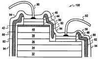
- the thin-film layer 86is then patterned to expose the p and n contact pads 46 and 50 using a suitable solvent (which will depend on the composition of the thin-film layer 86 ). Bonding wires 90 and 92 are then bonded to the p and n contact pads 46 and 50 , respectively.
- a second passivation layer 94is then formed over the structure of FIG. 7 .
- the first and second passivation layers 80 and 94are formed using the same process.
- the resultis a white-LED 100 .
- the white LED 100can then be encapsulated into a package, such as a lamp package or a surface mount package. However, the white LED 100 also can be used unpackaged and/or as part of another assembly.
- a reflectorbetween a contact pad and an adjacent semiconductor layer.
- a vertical LED 54is used as the blue light source, thus forming a white-light LED 101
- a reflective layer 104between the n-metal contact 56 and the n contact pad 57 .
- the second passiviation layer 94is beneficially over the p contact pad 68 .
- the second passivation layer 94is optional.
Landscapes
- Led Devices (AREA)
- Led Device Packages (AREA)
Abstract
Description
Claims (13)
Priority Applications (1)
| Application Number | Priority Date | Filing Date | Title |
|---|---|---|---|
| US11/544,645US7414271B2 (en) | 2002-12-11 | 2006-10-10 | Thin film led |
Applications Claiming Priority (3)
| Application Number | Priority Date | Filing Date | Title |
|---|---|---|---|
| US10/316,004US6744196B1 (en) | 2002-12-11 | 2002-12-11 | Thin film LED |
| US10/795,287US7420217B2 (en) | 2002-12-11 | 2004-03-09 | Thin film LED |
| US11/544,645US7414271B2 (en) | 2002-12-11 | 2006-10-10 | Thin film led |
Related Parent Applications (1)
| Application Number | Title | Priority Date | Filing Date |
|---|---|---|---|
| US10/795,287DivisionUS7420217B2 (en) | 2002-12-11 | 2004-03-09 | Thin film LED |
Publications (2)
| Publication Number | Publication Date |
|---|---|
| US20070048885A1 US20070048885A1 (en) | 2007-03-01 |
| US7414271B2true US7414271B2 (en) | 2008-08-19 |
Family
ID=32325907
Family Applications (3)
| Application Number | Title | Priority Date | Filing Date |
|---|---|---|---|
| US10/316,004Expired - LifetimeUS6744196B1 (en) | 2002-12-11 | 2002-12-11 | Thin film LED |
| US10/795,287Expired - LifetimeUS7420217B2 (en) | 2002-12-11 | 2004-03-09 | Thin film LED |
| US11/544,645Expired - LifetimeUS7414271B2 (en) | 2002-12-11 | 2006-10-10 | Thin film led |
Family Applications Before (2)
| Application Number | Title | Priority Date | Filing Date |
|---|---|---|---|
| US10/316,004Expired - LifetimeUS6744196B1 (en) | 2002-12-11 | 2002-12-11 | Thin film LED |
| US10/795,287Expired - LifetimeUS7420217B2 (en) | 2002-12-11 | 2004-03-09 | Thin film LED |
Country Status (1)
| Country | Link |
|---|---|
| US (3) | US6744196B1 (en) |
Cited By (2)
| Publication number | Priority date | Publication date | Assignee | Title |
|---|---|---|---|---|
| US8858031B2 (en) | 2010-07-22 | 2014-10-14 | Independence Led Lighting, Llc | Light engine device with direct to linear system driver |
| US20160172545A1 (en)* | 2013-07-16 | 2016-06-16 | Osram Opto Semiconductors Gmbh | Optoelectronic Semiconductor Chip |
Families Citing this family (78)
| Publication number | Priority date | Publication date | Assignee | Title |
|---|---|---|---|---|
| US7067849B2 (en) | 2001-07-17 | 2006-06-27 | Lg Electronics Inc. | Diode having high brightness and method thereof |
| US6949395B2 (en) | 2001-10-22 | 2005-09-27 | Oriol, Inc. | Method of making diode having reflective layer |
| US7148520B2 (en) | 2001-10-26 | 2006-12-12 | Lg Electronics Inc. | Diode having vertical structure and method of manufacturing the same |
| US20030189215A1 (en) | 2002-04-09 | 2003-10-09 | Jong-Lam Lee | Method of fabricating vertical structure leds |
| US8294172B2 (en)* | 2002-04-09 | 2012-10-23 | Lg Electronics Inc. | Method of fabricating vertical devices using a metal support film |
| US6841802B2 (en)* | 2002-06-26 | 2005-01-11 | Oriol, Inc. | Thin film light emitting diode |
| JP5142523B2 (en)* | 2003-06-04 | 2013-02-13 | チェオル ユー,ミュング | Vertical structure composite semiconductor device |
| JP2007525016A (en)* | 2003-07-14 | 2007-08-30 | アリージス・テクノロジーズ・インコーポレーテッド | Method for treating gallium nitride |
| KR101034055B1 (en)* | 2003-07-18 | 2011-05-12 | 엘지이노텍 주식회사 | Light emitting diodes and manufacturing method |
| US20050156510A1 (en)* | 2004-01-21 | 2005-07-21 | Chua Janet B.Y. | Device and method for emitting output light using group IIB element selenide-based and group IIA element gallium sulfide-based phosphor materials |
| US20050167684A1 (en)* | 2004-01-21 | 2005-08-04 | Chua Janet B.Y. | Device and method for emitting output light using group IIB element selenide-based phosphor material |
| EP1749308A4 (en)* | 2004-04-28 | 2011-12-28 | Verticle Inc | SEMICONDUCTOR DEVICES WITH VERTICAL STRUCTURE |
| TWI433343B (en)* | 2004-06-22 | 2014-04-01 | Verticle Inc | Vertical structure semiconductor device with improved light output |
| US7329905B2 (en)* | 2004-06-30 | 2008-02-12 | Cree, Inc. | Chip-scale methods for packaging light emitting devices and chip-scale packaged light emitting devices |
| US6993954B1 (en)* | 2004-07-27 | 2006-02-07 | Tekscan, Incorporated | Sensor equilibration and calibration system and method |
| DE102004060358A1 (en)* | 2004-09-30 | 2006-04-13 | Osram Opto Semiconductors Gmbh | Method for producing luminescence diode chips and luminescence diode chip |
| TWI389334B (en)* | 2004-11-15 | 2013-03-11 | Verticle Inc | Method of manufacturing and separating semiconductor devices |
| US7646033B2 (en) | 2005-01-11 | 2010-01-12 | Semileds Corporation | Systems and methods for producing white-light light emitting diodes |
| US7195944B2 (en)* | 2005-01-11 | 2007-03-27 | Semileds Corporation | Systems and methods for producing white-light emitting diodes |
| US8012774B2 (en)* | 2005-01-11 | 2011-09-06 | SemiLEDs Optoelectronics Co., Ltd. | Coating process for a light-emitting diode (LED) |
| US8680534B2 (en) | 2005-01-11 | 2014-03-25 | Semileds Corporation | Vertical light emitting diodes (LED) having metal substrate and spin coated phosphor layer for producing white light |
| TWI422044B (en)* | 2005-06-30 | 2014-01-01 | Cree Inc | Wafer-scale method for packaging light-emitting device and light-emitting device packaged by wafer scale |
| TWI291244B (en)* | 2005-07-07 | 2007-12-11 | Formosa Epitaxy Inc | Light emitting diode and light emitting diode package |
| EP1920285A4 (en)* | 2005-07-28 | 2010-11-03 | Light Prescriptions Innovators | OPEN-FREE LENTICULAR OPTICAL ELEMENTS AND THEIR APPLICATION TO CAPACITORS AND PROJECTORS |
| WO2007014371A2 (en)* | 2005-07-28 | 2007-02-01 | Light Prescriptions Innovators, Llc | Etendue-conserving illumination-optics for backlights and frontlights |
| JP5016808B2 (en)* | 2005-11-08 | 2012-09-05 | ローム株式会社 | Nitride semiconductor light emitting device and method for manufacturing nitride semiconductor light emitting device |
| US7829909B2 (en)* | 2005-11-15 | 2010-11-09 | Verticle, Inc. | Light emitting diodes and fabrication methods thereof |
| TWI291249B (en)* | 2005-12-12 | 2007-12-11 | San-Bau Lin | Light emitting device capable of enhancing reflection efficiency |
| US20070145879A1 (en)* | 2005-12-22 | 2007-06-28 | Abramov Vladimir S | Light emitting halogen-silicate photophosphor compositions and systems |
| US9443903B2 (en) | 2006-06-30 | 2016-09-13 | Cree, Inc. | Low temperature high strength metal stack for die attachment |
| US8698184B2 (en)* | 2011-01-21 | 2014-04-15 | Cree, Inc. | Light emitting diodes with low junction temperature and solid state backlight components including light emitting diodes with low junction temperature |
| WO2008008994A2 (en)* | 2006-07-14 | 2008-01-17 | Light Prescriptions Innovators, Llc | Brightness-enhancing film |
| EP2057409A2 (en)* | 2006-08-10 | 2009-05-13 | Light Prescriptions Innovators, LLC. | Led light recycling for luminance enhancement and angular narrowing |
| WO2008022065A2 (en)* | 2006-08-11 | 2008-02-21 | Light Prescriptions Innovators, Llc | Led luminance-enhancement and color-mixing by rotationally multiplexed beam-combining |
| TW200822788A (en)* | 2006-11-09 | 2008-05-16 | Univ Nat Central | Method of using laser in fabricating GaN device |
| US9196799B2 (en) | 2007-01-22 | 2015-11-24 | Cree, Inc. | LED chips having fluorescent substrates with microholes and methods for fabricating |
| US9159888B2 (en)* | 2007-01-22 | 2015-10-13 | Cree, Inc. | Wafer level phosphor coating method and devices fabricated utilizing method |
| US8232564B2 (en)* | 2007-01-22 | 2012-07-31 | Cree, Inc. | Wafer level phosphor coating technique for warm light emitting diodes |
| US9024349B2 (en)* | 2007-01-22 | 2015-05-05 | Cree, Inc. | Wafer level phosphor coating method and devices fabricated utilizing method |
| CN101271944B (en)* | 2007-03-22 | 2010-07-14 | 沈育浓 | Light emitting diode chip package and packaging method thereof |
| KR20090002835A (en)* | 2007-07-04 | 2009-01-09 | 엘지전자 주식회사 | Nitride-based light emitting device and its manufacturing method |
| US7846751B2 (en)* | 2007-11-19 | 2010-12-07 | Wang Nang Wang | LED chip thermal management and fabrication methods |
| US9041285B2 (en) | 2007-12-14 | 2015-05-26 | Cree, Inc. | Phosphor distribution in LED lamps using centrifugal force |
| US8167674B2 (en)* | 2007-12-14 | 2012-05-01 | Cree, Inc. | Phosphor distribution in LED lamps using centrifugal force |
| KR101491139B1 (en)* | 2007-12-20 | 2015-02-06 | 엘지이노텍 주식회사 | Semiconductor light emitting device and fabrication method thereof |
| US7943942B2 (en)* | 2008-03-25 | 2011-05-17 | Lattice Power (Jiangxi) Corporation | Semiconductor light-emitting device with double-sided passivation |
| CN102067345A (en)* | 2008-08-19 | 2011-05-18 | 晶能光电(江西)有限公司 | Method for fabricating semiconductor light-emitting device with double-sided passivation |
| WO2010020067A1 (en)* | 2008-08-19 | 2010-02-25 | Lattice Power (Jiangxi) Corporation | Semiconductor light-emitting device with passivation layer |
| US8102114B2 (en)* | 2009-02-27 | 2012-01-24 | Global Oled Technology, Llc. | Method of manufacturing an inverted bottom-emitting OLED device |
| CN101859845B (en)* | 2009-04-07 | 2016-07-13 | 江苏璨扬光电有限公司 | Light-emitting device and manufacture method thereof |
| KR101039931B1 (en)* | 2009-10-21 | 2011-06-09 | 엘지이노텍 주식회사 | Light emitting device and manufacturing method |
| KR100999779B1 (en)* | 2010-02-01 | 2010-12-08 | 엘지이노텍 주식회사 | Light emitting device, manufacturing method and light emitting device package |
| EP2933629B1 (en) | 2010-02-19 | 2019-04-10 | Pacific Biosciences Of California, Inc. | System for measuring analytical reactions comprising a socket for an optode array chip |
| JP2011233783A (en)* | 2010-04-28 | 2011-11-17 | Mitsubishi Heavy Ind Ltd | Semiconductor light-emitting device, protection film thereof, and its manufacturing method |
| US10546846B2 (en) | 2010-07-23 | 2020-01-28 | Cree, Inc. | Light transmission control for masking appearance of solid state light sources |
| KR100988194B1 (en) | 2010-07-26 | 2010-10-18 | (주)더리즈 | Semiconductor light emitting device and method of fabricating the same |
| US20120032212A1 (en)* | 2010-08-06 | 2012-02-09 | Taiwan Semiconductor Manufacturing Company, Ltd. | Method of light emitting diode sidewall passivation |
| KR101707118B1 (en)* | 2010-10-19 | 2017-02-15 | 엘지이노텍 주식회사 | Light emitting diode and method for fabricating the light emitting device |
| CN102456812B (en)* | 2010-10-28 | 2015-08-12 | 展晶科技(深圳)有限公司 | Package structure for LED |
| CN103443942A (en)* | 2011-03-31 | 2013-12-11 | 松下电器产业株式会社 | Semiconductor light emitting element and light emitting device |
| DE102011016302A1 (en)* | 2011-04-07 | 2012-10-11 | Osram Opto Semiconductors Gmbh | Optoelectronic semiconductor chip |
| TWI506820B (en)* | 2011-07-07 | 2015-11-01 | Lextar Electronics Corp | Method of coating phosphor and light emitting diode package |
| US8410508B1 (en) | 2011-09-12 | 2013-04-02 | SemiLEDs Optoelectronics Co., Ltd. | Light emitting diode (LED) package having wavelength conversion member and wafer level fabrication method |
| US8841146B2 (en) | 2011-09-12 | 2014-09-23 | SemiLEDs Optoelectronics Co., Ltd. | Method and system for fabricating light emitting diode (LED) dice with wavelength conversion layers having controlled color characteristics |
| US8492746B2 (en) | 2011-09-12 | 2013-07-23 | SemiLEDs Optoelectronics Co., Ltd. | Light emitting diode (LED) dice having wavelength conversion layers |
| US8912021B2 (en) | 2011-09-12 | 2014-12-16 | SemiLEDs Optoelectronics Co., Ltd. | System and method for fabricating light emitting diode (LED) dice with wavelength conversion layers |
| JP5857786B2 (en)* | 2012-02-21 | 2016-02-10 | 日亜化学工業株式会社 | Manufacturing method of semiconductor light emitting device |
| KR101962119B1 (en)* | 2012-08-23 | 2019-03-26 | 엘지이노텍 주식회사 | Light emitting device |
| US9269662B2 (en)* | 2012-10-17 | 2016-02-23 | Cree, Inc. | Using stress reduction barrier sub-layers in a semiconductor die |
| JP5915504B2 (en)* | 2012-11-06 | 2016-05-11 | 日亜化学工業株式会社 | Semiconductor light emitting device |
| US20140151630A1 (en)* | 2012-12-04 | 2014-06-05 | Feng-Hsu Fan | Protection for the epitaxial structure of metal devices |
| CN104377287B (en)* | 2013-08-14 | 2017-04-26 | 展晶科技(深圳)有限公司 | Light-emitting diode and manufacturing method thereof |
| CN104766913A (en)* | 2015-03-30 | 2015-07-08 | 映瑞光电科技(上海)有限公司 | LED structure and manufacturing method thereof |
| US10454239B2 (en) | 2015-08-28 | 2019-10-22 | International Business Machines Corporation | Wafer scale monolithic integration of lasers, modulators, and other optical components using ALD optical coatings |
| CN106252470B (en)* | 2016-08-30 | 2018-08-14 | 厦门市三安光电科技有限公司 | A kind of gallium nitride based light emitting diode and preparation method thereof |
| CN109994592B (en)* | 2016-10-20 | 2021-10-19 | 苏州星烁纳米科技有限公司 | Quantum dot colloid, light conversion element and light-emitting device |
| KR20190137458A (en)* | 2018-06-01 | 2019-12-11 | 삼성전자주식회사 | Method of display module using light emitting diode |
| CN113851563B (en)* | 2021-08-26 | 2023-11-21 | 江苏宜兴德融科技有限公司 | Thin film type semiconductor chip structure and photoelectric device using same |
Citations (8)
| Publication number | Priority date | Publication date | Assignee | Title |
|---|---|---|---|---|
| US3774086A (en) | 1972-09-25 | 1973-11-20 | Gen Electric | Solid state lamp having visible-emitting phosphor at edge of infrated-emitting element |
| US3875456A (en) | 1972-04-04 | 1975-04-01 | Hitachi Ltd | Multi-color semiconductor lamp |
| US5813753A (en) | 1997-05-27 | 1998-09-29 | Philips Electronics North America Corporation | UV/blue led-phosphor device with efficient conversion of UV/blues light to visible light |
| US5847507A (en) | 1997-07-14 | 1998-12-08 | Hewlett-Packard Company | Fluorescent dye added to epoxy of light emitting diode lens |
| US5998925A (en) | 1996-07-29 | 1999-12-07 | Nichia Kagaku Kogyo Kabushiki Kaisha | Light emitting device having a nitride compound semiconductor and a phosphor containing a garnet fluorescent material |
| US6337536B1 (en) | 1998-07-09 | 2002-01-08 | Sumitomo Electric Industries, Ltd. | White color light emitting diode and neutral color light emitting diode |
| US6600175B1 (en) | 1996-03-26 | 2003-07-29 | Advanced Technology Materials, Inc. | Solid state white light emitter and display using same |
| US6841802B2 (en)* | 2002-06-26 | 2005-01-11 | Oriol, Inc. | Thin film light emitting diode |
Family Cites Families (1)
| Publication number | Priority date | Publication date | Assignee | Title |
|---|---|---|---|---|
| EP0652400B1 (en)* | 1993-11-05 | 2000-09-20 | Vari-Lite, Inc. | Light pattern generator (gobo) and laser ablation method and apparatus for making it |
- 2002
- 2002-12-11USUS10/316,004patent/US6744196B1/ennot_activeExpired - Lifetime
- 2004
- 2004-03-09USUS10/795,287patent/US7420217B2/ennot_activeExpired - Lifetime
- 2006
- 2006-10-10USUS11/544,645patent/US7414271B2/ennot_activeExpired - Lifetime
Patent Citations (8)
| Publication number | Priority date | Publication date | Assignee | Title |
|---|---|---|---|---|
| US3875456A (en) | 1972-04-04 | 1975-04-01 | Hitachi Ltd | Multi-color semiconductor lamp |
| US3774086A (en) | 1972-09-25 | 1973-11-20 | Gen Electric | Solid state lamp having visible-emitting phosphor at edge of infrated-emitting element |
| US6600175B1 (en) | 1996-03-26 | 2003-07-29 | Advanced Technology Materials, Inc. | Solid state white light emitter and display using same |
| US5998925A (en) | 1996-07-29 | 1999-12-07 | Nichia Kagaku Kogyo Kabushiki Kaisha | Light emitting device having a nitride compound semiconductor and a phosphor containing a garnet fluorescent material |
| US5813753A (en) | 1997-05-27 | 1998-09-29 | Philips Electronics North America Corporation | UV/blue led-phosphor device with efficient conversion of UV/blues light to visible light |
| US5847507A (en) | 1997-07-14 | 1998-12-08 | Hewlett-Packard Company | Fluorescent dye added to epoxy of light emitting diode lens |
| US6337536B1 (en) | 1998-07-09 | 2002-01-08 | Sumitomo Electric Industries, Ltd. | White color light emitting diode and neutral color light emitting diode |
| US6841802B2 (en)* | 2002-06-26 | 2005-01-11 | Oriol, Inc. | Thin film light emitting diode |
Non-Patent Citations (4)
| Title |
|---|
| Authors: Mensz, P. M.; Kellawon, P.; van Rojen, R.; Kozodoy, P.; Denbaars, S.; Titled: "In<SUB>x</SUB>Ga<SUB>1-x</SUB>N/AI<SUB>y</SUB>Ga<SUB>1-y</SUB>N violet light emitting diodes with reflective p-contacts for high single sided light extraction": Electronics Letters; 20<SUP>th </SUP>Nov. 1997; vol. 33-No. 24. |
| Michael Kneissl, et al., "Continuous-Wave Operation of InGaN Multiple-Quantum-Well Laser Diodes on Copper Substrates Obtained by Laser Liftoff", IEEE Journal on Selected Topics in Quantum Electronics, vol. 7, No. 2, Mar./Apr. 2001; pp. 188-191. |
| William S. Wong, et al., "Continuous-Wave Operation of InGaN Multiple-Quantum-Well Laser Diodes on Copper Substrates", Applied Physics Letters vol. 78, No. 9, Feb. 26, 2001; pp. 1198-1200. |
| William S. Wong, et al., "The integration of IN<SUB>x</SUB>GA<SUB>1-x</SUB>N Multiple-Quantum-Well Laser Diodes with Copper Substrates by Laser Lift-Off", Jpn. J. Appl. Phys. vol. 39 (2000) pp. L 1203-L1205, Part 2, No. 12A, Dec. 1, 2000; pp. L 1203-L 1205. |
Cited By (3)
| Publication number | Priority date | Publication date | Assignee | Title |
|---|---|---|---|---|
| US8858031B2 (en) | 2010-07-22 | 2014-10-14 | Independence Led Lighting, Llc | Light engine device with direct to linear system driver |
| US20160172545A1 (en)* | 2013-07-16 | 2016-06-16 | Osram Opto Semiconductors Gmbh | Optoelectronic Semiconductor Chip |
| US10014444B2 (en)* | 2013-07-16 | 2018-07-03 | Osram Opto Semiconductors Gmbh | Optoelectronic semiconductor chip |
Also Published As
| Publication number | Publication date |
|---|---|
| US20070048885A1 (en) | 2007-03-01 |
| US7420217B2 (en) | 2008-09-02 |
| US20040169189A1 (en) | 2004-09-02 |
| US6744196B1 (en) | 2004-06-01 |
Similar Documents
| Publication | Publication Date | Title |
|---|---|---|
| US10825962B2 (en) | Thin film light emitting diode | |
| US7414271B2 (en) | Thin film led | |
| US10043955B2 (en) | Light emitting diode chip having wavelength converting layer and method of fabricating the same, and package having the light emitting diode chip and method of fabricating the same | |
| US5557115A (en) | Light emitting semiconductor device with sub-mount | |
| KR100491314B1 (en) | Light emitting device | |
| JP3282176B2 (en) | Method of forming light emitting diode | |
| US20120104418A1 (en) | Light-emitting module and alternating current light-emitting device | |
| KR100670929B1 (en) | Light emitting device of flip chip structure and manufacturing method thereof | |
| KR100450514B1 (en) | White light emitting diode | |
| KR100901370B1 (en) | White light emitting diode chip having electrostatic discharge protection function and manufacturing method thereof | |
| JP2001156330A (en) | Light emitting diode |
Legal Events
| Date | Code | Title | Description |
|---|---|---|---|
| AS | Assignment | Owner name:LG ELECTRONICS, KOREA, REPUBLIC OF Free format text:ASSIGNMENT OF ASSIGNORS INTEREST;ASSIGNOR:ORIOL, INC. (CAROL W. WU, TRUSTEE IN BANKRUPTCY OF THE ESTATE OF ORIOL, INC.);REEL/FRAME:018406/0676 Effective date:20050803 | |
| FEPP | Fee payment procedure | Free format text:PAYOR NUMBER ASSIGNED (ORIGINAL EVENT CODE: ASPN); ENTITY STATUS OF PATENT OWNER: LARGE ENTITY | |
| STCF | Information on status: patent grant | Free format text:PATENTED CASE | |
| FEPP | Fee payment procedure | Free format text:PAYER NUMBER DE-ASSIGNED (ORIGINAL EVENT CODE: RMPN); ENTITY STATUS OF PATENT OWNER: LARGE ENTITY Free format text:PAYOR NUMBER ASSIGNED (ORIGINAL EVENT CODE: ASPN); ENTITY STATUS OF PATENT OWNER: LARGE ENTITY | |
| FPAY | Fee payment | Year of fee payment:4 | |
| AS | Assignment | Owner name:LG INNOTEK CO. LTD., KOREA, REPUBLIC OF Free format text:ASSIGNMENT OF ASSIGNORS INTEREST;ASSIGNOR:LG ELECTRONICS, INC.;REEL/FRAME:031410/0169 Effective date:20130916 | |
| FPAY | Fee payment | Year of fee payment:8 | |
| MAFP | Maintenance fee payment | Free format text:PAYMENT OF MAINTENANCE FEE, 12TH YEAR, LARGE ENTITY (ORIGINAL EVENT CODE: M1553); ENTITY STATUS OF PATENT OWNER: LARGE ENTITY Year of fee payment:12 | |
| AS | Assignment | Owner name:SUZHOU LEKIN SEMICONDUCTOR CO., LTD., CHINA Free format text:ASSIGNMENT OF ASSIGNORS INTEREST;ASSIGNOR:LG INNOTEK CO., LTD.;REEL/FRAME:056366/0335 Effective date:20210520 |