US7412566B2 - Memory hub and access method having internal prefetch buffers - Google Patents
Memory hub and access method having internal prefetch buffersDownload PDFInfo
- Publication number
- US7412566B2 US7412566B2US11/510,150US51015006AUS7412566B2US 7412566 B2US7412566 B2US 7412566B2US 51015006 AUS51015006 AUS 51015006AUS 7412566 B2US7412566 B2US 7412566B2
- Authority
- US
- United States
- Prior art keywords
- memory
- data
- prefetch
- requests
- coupled
- Prior art date
- Legal status (The legal status is an assumption and is not a legal conclusion. Google has not performed a legal analysis and makes no representation as to the accuracy of the status listed.)
- Expired - Fee Related, expires
Links
Images


Classifications
- G—PHYSICS
- G06—COMPUTING OR CALCULATING; COUNTING
- G06F—ELECTRIC DIGITAL DATA PROCESSING
- G06F12/00—Accessing, addressing or allocating within memory systems or architectures
- G06F12/02—Addressing or allocation; Relocation
- G06F12/08—Addressing or allocation; Relocation in hierarchically structured memory systems, e.g. virtual memory systems
- G06F12/0802—Addressing of a memory level in which the access to the desired data or data block requires associative addressing means, e.g. caches
- G06F12/0862—Addressing of a memory level in which the access to the desired data or data block requires associative addressing means, e.g. caches with prefetch
- G—PHYSICS
- G06—COMPUTING OR CALCULATING; COUNTING
- G06F—ELECTRIC DIGITAL DATA PROCESSING
- G06F2212/00—Indexing scheme relating to accessing, addressing or allocation within memory systems or architectures
- G06F2212/60—Details of cache memory
- G06F2212/6022—Using a prefetch buffer or dedicated prefetch cache
- G—PHYSICS
- G06—COMPUTING OR CALCULATING; COUNTING
- G06F—ELECTRIC DIGITAL DATA PROCESSING
- G06F2212/00—Indexing scheme relating to accessing, addressing or allocation within memory systems or architectures
- G06F2212/60—Details of cache memory
- G06F2212/6024—History based prefetching
- G—PHYSICS
- G06—COMPUTING OR CALCULATING; COUNTING
- G06F—ELECTRIC DIGITAL DATA PROCESSING
- G06F2212/00—Indexing scheme relating to accessing, addressing or allocation within memory systems or architectures
- G06F2212/60—Details of cache memory
- G06F2212/6026—Prefetching based on access pattern detection, e.g. stride based prefetch
Definitions
- This inventionrelates to computer systems, and, more particularly, to a computer system having a memory hub coupling several memory devices to a processor or other memory access device.
- Computer systemsuse memory devices, such as dynamic random access memory (“DRAM”) devices, to store data that are accessed by a processor. These memory devices are normally used as system memory in a computer system.
- the processorcommunicates with the system memory through a processor bus and a memory controller.
- the processorissues a memory request, which includes a memory command, such as a read command, and an address designating the location from which data or instructions are to be read.
- the memory controlleruses the command and address to generate appropriate command signals as well as row and column addresses, which are applied to the system memory.
- dataare transferred between the system memory and the processor.
- the memory controlleris often part of a system controller, which also includes bus bridge circuitry for coupling the processor bus to an expansion bus, such as a PCI bus.
- One approach to alleviating the memory latency problemis to use multiple memory devices coupled to the processor through a memory hub.
- a system controller or memory controlleris coupled to several memory modules, each of which includes a memory hub coupled to several memory devices.
- the memory hubefficiently routes memory requests and responses between the controller and the memory devices.
- Computer systems employing this architecturecan have a higher bandwidth because a processor can access one memory device while another memory device is responding to a prior memory access. For example, the processor can output write data to one of the memory devices in the system while another memory device in the system is preparing to provide read data to the processor.
- computer systems using memory hubsmay provide superior performance, they nevertheless often fail to operate at optimum speed for several reasons.
- memory hubscan provide computer systems with a greater memory bandwidth, they still suffer from latency problems of the type described above. More specifically, although the processor may communicate with one memory device while another memory device is preparing to transfer data, it is sometimes necessary to receive data from one memory device before the data from another memory device can be used. In the event data must be received from one memory device before data received from another memory device can be used, the latency problem continues to slow the operating speed of such computer systems.
- One technique that has been used to reduce latency in memory devicesis to prefetch data, i.e., read data from system memory before the data are requested by a program being executed.
- data that are to be prefetchedare selected based on a pattern of previously fetched data.
- the patternmay be as simple as a sequence of addresses from which data are fetched so that data can be fetched from subsequent addresses in the sequence before the data are needed by the program being executed.
- the patternwhich is known as a “stride,” may, of course, be more complex.
- prefetchingcan reduce memory access latencies in conventional computer systems
- prefetching of datahas not been effectively used in a manner that provides optimum performance in computer systems using memory hubs.
- the vast amount of data that can be addressed in a computer system having several memory hubsmakes it difficult to accurately predict which data will be subsequently needed.
- the need to couple the data from the memory module to the prefetch buffercan also reduce the memory bandwidth of the system if the data are being prefetched at a time when normal memory accesses are being attempted.
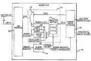
- FIG. 1is a block diagram of a computer system according to one example of the invention in which a memory hub is included in each of a plurality of memory modules.
- Each of the memory modules 130includes a memory hub 140 for controlling access to 8 memory devices 148 , which, in the example illustrated in FIG. 2 , are synchronous dynamic random access memory (“SDRAM”) devices. However, a fewer or greater number of memory devices 148 may be used, and memory devices other than SDRAM devices may, of course, also be used.
- the memory hub 140is coupled to each of the system memory devices 148 through a bus system 150 , which normally includes a control bus, an address bus and a data bus.
- the link interface 152may include a variety of conventional interface circuitry such as, for example, a first-in, first-out buffer (not shown), for receiving and storing memory requests as they are received through the high-speed link 134 .
- the memory requestscan then be stored in the link interface until they can be processed by the memory hub 140 .
- the memory device interface 166may re-order the memory requests so that they are applied to the memory devices 148 in some other order.
- the memory requestsmay be stored in the interface 166 in a manner that causes one type of request, e.g., read requests, to be processed before other types of requests, e.g., write requests.
- datamay be prefetched from any address in the memory devices 148
- the dataare preferably prefetched only from rows in the memory devices 148 that are currently active or “open” so that the prefetching will not require a row of memory cells in the memory devices 148 to be precharged.
- the tag logic 186stores the prefetch addresses to provide a record of the data that have been stored in the prefetch buffers 176 .
- the tag logic 186compares the address in each memory request received from the link interface 152 with the prefetch addresses stored in the tag logic 186 to determine if the data called for by the memory request are stored in the prefetch buffers 176 . If the tag logic 186 determines the data are not stored in the prefetch buffers. 176 , it couples a low HIT/MISS* signal to the memory sequencer 160 .
Landscapes
- Engineering & Computer Science (AREA)
- Theoretical Computer Science (AREA)
- Physics & Mathematics (AREA)
- General Engineering & Computer Science (AREA)
- General Physics & Mathematics (AREA)
- Memory System Of A Hierarchy Structure (AREA)
Abstract
Description
Claims (73)
Priority Applications (2)
| Application Number | Priority Date | Filing Date | Title |
|---|---|---|---|
| US11/510,150US7412566B2 (en) | 2003-06-20 | 2006-08-24 | Memory hub and access method having internal prefetch buffers |
| US12/185,615US8127081B2 (en) | 2003-06-20 | 2008-08-04 | Memory hub and access method having internal prefetch buffers |
Applications Claiming Priority (2)
| Application Number | Priority Date | Filing Date | Title |
|---|---|---|---|
| US10/601,252US7260685B2 (en) | 2003-06-20 | 2003-06-20 | Memory hub and access method having internal prefetch buffers |
| US11/510,150US7412566B2 (en) | 2003-06-20 | 2006-08-24 | Memory hub and access method having internal prefetch buffers |
Related Parent Applications (1)
| Application Number | Title | Priority Date | Filing Date |
|---|---|---|---|
| US10/601,252ContinuationUS7260685B2 (en) | 2003-06-20 | 2003-06-20 | Memory hub and access method having internal prefetch buffers |
Related Child Applications (1)
| Application Number | Title | Priority Date | Filing Date |
|---|---|---|---|
| US12/185,615ContinuationUS8127081B2 (en) | 2003-06-20 | 2008-08-04 | Memory hub and access method having internal prefetch buffers |
Publications (2)
| Publication Number | Publication Date |
|---|---|
| US20060288172A1 US20060288172A1 (en) | 2006-12-21 |
| US7412566B2true US7412566B2 (en) | 2008-08-12 |
Family
ID=33517934
Family Applications (3)
| Application Number | Title | Priority Date | Filing Date |
|---|---|---|---|
| US10/601,252Expired - Fee RelatedUS7260685B2 (en) | 2003-06-20 | 2003-06-20 | Memory hub and access method having internal prefetch buffers |
| US11/510,150Expired - Fee RelatedUS7412566B2 (en) | 2003-06-20 | 2006-08-24 | Memory hub and access method having internal prefetch buffers |
| US12/185,615Expired - Fee RelatedUS8127081B2 (en) | 2003-06-20 | 2008-08-04 | Memory hub and access method having internal prefetch buffers |
Family Applications Before (1)
| Application Number | Title | Priority Date | Filing Date |
|---|---|---|---|
| US10/601,252Expired - Fee RelatedUS7260685B2 (en) | 2003-06-20 | 2003-06-20 | Memory hub and access method having internal prefetch buffers |
Family Applications After (1)
| Application Number | Title | Priority Date | Filing Date |
|---|---|---|---|
| US12/185,615Expired - Fee RelatedUS8127081B2 (en) | 2003-06-20 | 2008-08-04 | Memory hub and access method having internal prefetch buffers |
Country Status (1)
| Country | Link |
|---|---|
| US (3) | US7260685B2 (en) |
Cited By (17)
| Publication number | Priority date | Publication date | Assignee | Title |
|---|---|---|---|---|
| US20080183959A1 (en)* | 2007-01-29 | 2008-07-31 | Pelley Perry H | Memory system having global buffered control for memory modules |
| US7490217B2 (en) | 2006-08-15 | 2009-02-10 | International Business Machines Corporation | Design structure for selecting memory busses according to physical memory organization information stored in virtual address translation tables |
| US7539842B2 (en) | 2006-08-15 | 2009-05-26 | International Business Machines Corporation | Computer memory system for selecting memory buses according to physical memory organization information stored in virtual address translation tables |
| US7610423B2 (en) | 2004-10-29 | 2009-10-27 | International Business Machines Corporation | Service interface to a memory system |
| US20100095070A1 (en)* | 2007-06-19 | 2010-04-15 | Fujitsu Limited | Information processing apparatus and cache memory control method |
| US7934115B2 (en) | 2005-10-31 | 2011-04-26 | International Business Machines Corporation | Deriving clocks in a memory system |
| US7945737B2 (en) | 2002-06-07 | 2011-05-17 | Round Rock Research, Llc | Memory hub with internal cache and/or memory access prediction |
| US20110131380A1 (en)* | 2009-11-30 | 2011-06-02 | Rallens Tyson D | Altering prefetch depth based on ready data |
| US8127081B2 (en) | 2003-06-20 | 2012-02-28 | Round Rock Research, Llc | Memory hub and access method having internal prefetch buffers |
| US8239607B2 (en) | 2004-06-04 | 2012-08-07 | Micron Technology, Inc. | System and method for an asynchronous data buffer having buffer write and read pointers |
| US8296541B2 (en) | 2004-10-29 | 2012-10-23 | International Business Machines Corporation | Memory subsystem with positional read data latency |
| US8327105B2 (en) | 2005-11-28 | 2012-12-04 | International Business Machines Corporation | Providing frame start indication in a memory system having indeterminate read data latency |
| US8381064B2 (en) | 2006-10-23 | 2013-02-19 | International Business Machines Corporation | High density high reliability memory module with power gating and a fault tolerant address and command bus |
| US20130086335A1 (en)* | 2010-05-27 | 2013-04-04 | Fujitsu Limited | Memory system and memory interface device |
| US8589769B2 (en) | 2004-10-29 | 2013-11-19 | International Business Machines Corporation | System, method and storage medium for providing fault detection and correction in a memory subsystem |
| US10838869B1 (en)* | 2018-12-11 | 2020-11-17 | Amazon Technologies, Inc. | Predictive prefetch of a memory page |
| US20230060194A1 (en)* | 2021-08-30 | 2023-03-02 | International Business Machines Corporation | Dynamically allocating memory controller resources for extended prefetching |
Families Citing this family (50)
| Publication number | Priority date | Publication date | Assignee | Title |
|---|---|---|---|---|
| US6791555B1 (en) | 2000-06-23 | 2004-09-14 | Micron Technology, Inc. | Apparatus and method for distributed memory control in a graphics processing system |
| US7117316B2 (en) | 2002-08-05 | 2006-10-03 | Micron Technology, Inc. | Memory hub and access method having internal row caching |
| US6820181B2 (en) | 2002-08-29 | 2004-11-16 | Micron Technology, Inc. | Method and system for controlling memory accesses to memory modules having a memory hub architecture |
| US7120727B2 (en) | 2003-06-19 | 2006-10-10 | Micron Technology, Inc. | Reconfigurable memory module and method |
| US7107415B2 (en)* | 2003-06-20 | 2006-09-12 | Micron Technology, Inc. | Posted write buffers and methods of posting write requests in memory modules |
| US7133991B2 (en)* | 2003-08-20 | 2006-11-07 | Micron Technology, Inc. | Method and system for capturing and bypassing memory transactions in a hub-based memory system |
| US7231495B2 (en)* | 2003-08-29 | 2007-06-12 | Hitachi Global Storage Technologies Netherlands B.V. | Speculative data streaming disk drive and system |
| US7120743B2 (en) | 2003-10-20 | 2006-10-10 | Micron Technology, Inc. | Arbitration system and method for memory responses in a hub-based memory system |
| US7330992B2 (en) | 2003-12-29 | 2008-02-12 | Micron Technology, Inc. | System and method for read synchronization of memory modules |
| US20050147414A1 (en)* | 2003-12-30 | 2005-07-07 | Morrow Warren R. | Low latency optical memory bus |
| US7188219B2 (en) | 2004-01-30 | 2007-03-06 | Micron Technology, Inc. | Buffer control system and method for a memory system having outstanding read and write request buffers |
| US7464250B2 (en)* | 2004-03-11 | 2008-12-09 | International Business Machines Corporation | Method to reduce disk access time during predictable loading sequences |
| US7213082B2 (en) | 2004-03-29 | 2007-05-01 | Micron Technology, Inc. | Memory hub and method for providing memory sequencing hints |
| US7162567B2 (en) | 2004-05-14 | 2007-01-09 | Micron Technology, Inc. | Memory hub and method for memory sequencing |
| US7224595B2 (en) | 2004-07-30 | 2007-05-29 | International Business Machines Corporation | 276-Pin buffered memory module with enhanced fault tolerance |
| US7389375B2 (en) | 2004-07-30 | 2008-06-17 | International Business Machines Corporation | System, method and storage medium for a multi-mode memory buffer device |
| US7539800B2 (en) | 2004-07-30 | 2009-05-26 | International Business Machines Corporation | System, method and storage medium for providing segment level sparing |
| US7296129B2 (en) | 2004-07-30 | 2007-11-13 | International Business Machines Corporation | System, method and storage medium for providing a serialized memory interface with a bus repeater |
| US7356737B2 (en) | 2004-10-29 | 2008-04-08 | International Business Machines Corporation | System, method and storage medium for testing a memory module |
| US7395476B2 (en) | 2004-10-29 | 2008-07-01 | International Business Machines Corporation | System, method and storage medium for providing a high speed test interface to a memory subsystem |
| US7305574B2 (en) | 2004-10-29 | 2007-12-04 | International Business Machines Corporation | System, method and storage medium for bus calibration in a memory subsystem |
| US7277988B2 (en) | 2004-10-29 | 2007-10-02 | International Business Machines Corporation | System, method and storage medium for providing data caching and data compression in a memory subsystem |
| US7299313B2 (en) | 2004-10-29 | 2007-11-20 | International Business Machines Corporation | System, method and storage medium for a memory subsystem command interface |
| US20060112230A1 (en)* | 2004-11-24 | 2006-05-25 | Christian Sichert | Integrated memory device and memory module |
| US7516291B2 (en) | 2005-11-21 | 2009-04-07 | Red Hat, Inc. | Cooperative mechanism for efficient application memory allocation |
| US7636813B2 (en) | 2006-05-22 | 2009-12-22 | International Business Machines Corporation | Systems and methods for providing remote pre-fetch buffers |
| US7640386B2 (en) | 2006-05-24 | 2009-12-29 | International Business Machines Corporation | Systems and methods for providing memory modules with multiple hub devices |
| US7594055B2 (en) | 2006-05-24 | 2009-09-22 | International Business Machines Corporation | Systems and methods for providing distributed technology independent memory controllers |
| US7584336B2 (en) | 2006-06-08 | 2009-09-01 | International Business Machines Corporation | Systems and methods for providing data modification operations in memory subsystems |
| US7493439B2 (en)* | 2006-08-01 | 2009-02-17 | International Business Machines Corporation | Systems and methods for providing performance monitoring in a memory system |
| US7669086B2 (en)* | 2006-08-02 | 2010-02-23 | International Business Machines Corporation | Systems and methods for providing collision detection in a memory system |
| US7581073B2 (en) | 2006-08-09 | 2009-08-25 | International Business Machines Corporation | Systems and methods for providing distributed autonomous power management in a memory system |
| US7587559B2 (en) | 2006-08-10 | 2009-09-08 | International Business Machines Corporation | Systems and methods for memory module power management |
| US7477522B2 (en) | 2006-10-23 | 2009-01-13 | International Business Machines Corporation | High density high reliability memory module with a fault tolerant address and command bus |
| US7721140B2 (en) | 2007-01-02 | 2010-05-18 | International Business Machines Corporation | Systems and methods for improving serviceability of a memory system |
| US7606988B2 (en) | 2007-01-29 | 2009-10-20 | International Business Machines Corporation | Systems and methods for providing a dynamic memory bank page policy |
| US7603526B2 (en) | 2007-01-29 | 2009-10-13 | International Business Machines Corporation | Systems and methods for providing dynamic memory pre-fetch |
| JP2008225915A (en)* | 2007-03-13 | 2008-09-25 | Fujitsu Ltd | Prefetch control device, storage system, and prefetch control method |
| US20100005206A1 (en)* | 2008-07-01 | 2010-01-07 | International Business Machines Corporation | Automatic read data flow control in a cascade interconnect memory system |
| KR101796116B1 (en) | 2010-10-20 | 2017-11-10 | 삼성전자 주식회사 | Semiconductor device, memory module and memory system having the same and operating method thereof |
| US20130262779A1 (en)* | 2012-03-30 | 2013-10-03 | Jayaram Bobba | Profile-based hardware prefetching |
| CN104583976B (en) | 2012-08-18 | 2017-10-17 | 高通科技公司 | With the translation lookaside buffer prefetched |
| US9880842B2 (en) | 2013-03-15 | 2018-01-30 | Intel Corporation | Using control flow data structures to direct and track instruction execution |
| KR102130578B1 (en)* | 2014-12-02 | 2020-07-06 | 에스케이하이닉스 주식회사 | Semiconductor device |
| US10613763B2 (en)* | 2016-04-21 | 2020-04-07 | Adesto Technologies Corporation | Memory device having multiple read buffers for read latency reduction |
| US10679722B2 (en) | 2016-08-26 | 2020-06-09 | Sandisk Technologies Llc | Storage system with several integrated components and method for use therewith |
| US10866897B2 (en)* | 2016-09-26 | 2020-12-15 | Samsung Electronics Co., Ltd. | Byte-addressable flash-based memory module with prefetch mode that is adjusted based on feedback from prefetch accuracy that is calculated by comparing first decoded address and second decoded address, where the first decoded address is sent to memory controller, and the second decoded address is sent to prefetch buffer |
| CN109783399B (en)* | 2018-11-19 | 2021-01-19 | 西安交通大学 | Data cache prefetching method of dynamic reconfigurable processor |
| US11169737B2 (en)* | 2019-08-13 | 2021-11-09 | Micron Technology, Inc. | Speculation in memory |
| CN120407468B (en)* | 2025-07-01 | 2025-09-30 | 北京青耘科技有限公司 | Memory controller and 3D stacked memory |
Citations (276)
| Publication number | Priority date | Publication date | Assignee | Title |
|---|---|---|---|---|
| US751703A (en)* | 1904-02-09 | Robert warriner | ||
| US3742253A (en) | 1971-03-15 | 1973-06-26 | Burroughs Corp | Three state logic device with applications |
| US4045781A (en) | 1976-02-13 | 1977-08-30 | Digital Equipment Corporation | Memory module with selectable byte addressing for digital data processing system |
| US4240143A (en) | 1978-12-22 | 1980-12-16 | Burroughs Corporation | Hierarchical multi-processor network for memory sharing |
| US4245306A (en) | 1978-12-21 | 1981-01-13 | Burroughs Corporation | Selection of addressed processor in a multi-processor network |
| US4253144A (en) | 1978-12-21 | 1981-02-24 | Burroughs Corporation | Multi-processor communication network |
| US4253146A (en) | 1978-12-21 | 1981-02-24 | Burroughs Corporation | Module for coupling computer-processors |
| US4608702A (en) | 1984-12-21 | 1986-08-26 | Advanced Micro Devices, Inc. | Method for digital clock recovery from Manchester-encoded signals |
| US4707823A (en) | 1986-07-21 | 1987-11-17 | Chrysler Motors Corporation | Fiber optic multiplexed data acquisition system |
| US4724520A (en) | 1985-07-01 | 1988-02-09 | United Technologies Corporation | Modular multiport data hub |
| US4831520A (en) | 1987-02-24 | 1989-05-16 | Digital Equipment Corporation | Bus interface circuit for digital data processor |
| US4891808A (en) | 1987-12-24 | 1990-01-02 | Coherent Communication Systems Corp. | Self-synchronizing multiplexer |
| US4930128A (en) | 1987-06-26 | 1990-05-29 | Hitachi, Ltd. | Method for restart of online computer system and apparatus for carrying out the same |
| US4953930A (en) | 1989-03-15 | 1990-09-04 | Ramtech, Inc. | CPU socket supporting socket-to-socket optical communications |
| US5133059A (en) | 1987-07-30 | 1992-07-21 | Alliant Computer Systems Corporation | Computer with multiple processors having varying priorities for access to a multi-element memory |
| US5241506A (en) | 1989-11-15 | 1993-08-31 | Kabushiki Kaisha Toshiba | Semiconductor memory circuit apparatus |
| US5243703A (en) | 1990-04-18 | 1993-09-07 | Rambus, Inc. | Apparatus for synchronously generating clock signals in a data processing system |
| WO1993019422A1 (en) | 1992-03-25 | 1993-09-30 | Encore Computer U.S., Inc. | Fiber optic memory coupling system |
| US5251303A (en) | 1989-01-13 | 1993-10-05 | International Business Machines Corporation | System for DMA block data transfer based on linked control blocks |
| US5269022A (en) | 1990-03-28 | 1993-12-07 | Kabushiki Kaisha Toshiba | Method and apparatus for booting a computer system by restoring the main memory from a backup memory |
| US5313590A (en) | 1990-01-05 | 1994-05-17 | Maspar Computer Corporation | System having fixedly priorized and grouped by positions I/O lines for interconnecting router elements in plurality of stages within parrallel computer |
| US5317752A (en) | 1989-12-22 | 1994-05-31 | Tandem Computers Incorporated | Fault-tolerant computer system with auto-restart after power-fall |
| US5319755A (en) | 1990-04-18 | 1994-06-07 | Rambus, Inc. | Integrated circuit I/O using high performance bus interface |
| US5327553A (en) | 1989-12-22 | 1994-07-05 | Tandem Computers Incorporated | Fault-tolerant computer system with /CONFIG filesystem |
| US5355391A (en) | 1992-03-06 | 1994-10-11 | Rambus, Inc. | High speed bus system |
| US5432823A (en) | 1992-03-06 | 1995-07-11 | Rambus, Inc. | Method and circuitry for minimizing clock-data skew in a bus system |
| US5432907A (en) | 1992-05-12 | 1995-07-11 | Network Resources Corporation | Network hub with integrated bridge |
| US5442770A (en) | 1989-01-24 | 1995-08-15 | Nec Electronics, Inc. | Triple port cache memory |
| US5461627A (en) | 1991-12-24 | 1995-10-24 | Rypinski; Chandos A. | Access protocol for a common channel wireless network |
| US5465229A (en) | 1992-05-19 | 1995-11-07 | Sun Microsystems, Inc. | Single in-line memory module |
| US5479370A (en) | 1992-02-20 | 1995-12-26 | Kabushiki Kaisha Toshiba | Semiconductor memory with bypass circuit |
| US5497476A (en) | 1992-09-21 | 1996-03-05 | International Business Machines Corporation | Scatter-gather in data processing system |
| US5502621A (en) | 1994-03-31 | 1996-03-26 | Hewlett-Packard Company | Mirrored pin assignment for two sided multi-chip layout |
| US5566325A (en) | 1994-06-30 | 1996-10-15 | Digital Equipment Corporation | Method and apparatus for adaptive memory access |
| US5577220A (en) | 1993-07-23 | 1996-11-19 | International Business Machines Corporation | Method for saving and restoring the state of a CPU executing code in protected mode including estimating the value of the page table base register |
| US5581767A (en) | 1993-06-16 | 1996-12-03 | Nippon Sheet Glass Co., Ltd. | Bus structure for multiprocessor system having separated processor section and control/memory section |
| US5638534A (en) | 1995-03-31 | 1997-06-10 | Samsung Electronics Co., Ltd. | Memory controller which executes read and write commands out of order |
| US5659798A (en) | 1996-02-02 | 1997-08-19 | Blumrich; Matthias Augustin | Method and system for initiating and loading DMA controller registers by using user-level programs |
| US5687325A (en) | 1996-04-19 | 1997-11-11 | Chang; Web | Application specific field programmable gate array |
| US5706224A (en) | 1996-10-10 | 1998-01-06 | Quality Semiconductor, Inc. | Content addressable memory and random access memory partition circuit |
| US5710733A (en) | 1996-01-22 | 1998-01-20 | Silicon Graphics, Inc. | Processor-inclusive memory module |
| US5715456A (en) | 1995-02-13 | 1998-02-03 | International Business Machines Corporation | Method and apparatus for booting a computer system without pre-installing an operating system |
| US5729709A (en) | 1993-11-12 | 1998-03-17 | Intel Corporation | Memory controller with burst addressing circuit |
| US5748616A (en) | 1994-09-13 | 1998-05-05 | Square D Company | Data link module for time division multiplexing control systems |
| EP0849685A2 (en) | 1996-12-19 | 1998-06-24 | Texas Instruments Incorporated | Communication bus system between processors and memory modules |
| US5796413A (en) | 1995-12-06 | 1998-08-18 | Compaq Computer Corporation | Graphics controller utilizing video memory to provide macro command capability and enhanched command buffering |
| US5819304A (en) | 1996-01-29 | 1998-10-06 | Iowa State University Research Foundation, Inc. | Random access memory assembly |
| US5818844A (en) | 1996-06-06 | 1998-10-06 | Advanced Micro Devices, Inc. | Address generation and data path arbitration to and from SRAM to accommodate multiple transmitted packets |
| US5822255A (en) | 1996-08-13 | 1998-10-13 | Fujitsu Limited | Semiconductor integrated circuit for supplying a control signal to a plurality of object circuits |
| US5832250A (en) | 1996-01-26 | 1998-11-03 | Unisys Corporation | Multi set cache structure having parity RAMs holding parity bits for tag data and for status data utilizing prediction circuitry that predicts and generates the needed parity bits |
| WO1998057489A2 (en) | 1997-06-09 | 1998-12-17 | Metalithic Systems, Inc. | Modular system for accelerating data searches and data stream operations |
| US5875352A (en) | 1995-11-03 | 1999-02-23 | Sun Microsystems, Inc. | Method and apparatus for multiple channel direct memory access control |
| US5875454A (en) | 1996-07-24 | 1999-02-23 | International Business Machiness Corporation | Compressed data cache storage system |
| US5887159A (en) | 1996-12-11 | 1999-03-23 | Digital Equipment Corporation | Dynamically determining instruction hint fields |
| US5889714A (en) | 1997-11-03 | 1999-03-30 | Digital Equipment Corporation | Adaptive precharge management for synchronous DRAM |
| US5963942A (en) | 1996-01-16 | 1999-10-05 | Fujitsu Limited | Pattern search apparatus and method |
| US5966724A (en) | 1996-01-11 | 1999-10-12 | Micron Technology, Inc. | Synchronous memory device with dual page and burst mode operations |
| US5973935A (en) | 1997-04-07 | 1999-10-26 | Micron Technology, Inc. | Interdigitated leads-over-chip lead frame for supporting an integrated circuit die |
| US5978567A (en) | 1994-07-27 | 1999-11-02 | Instant Video Technologies Inc. | System for distribution of interactive multimedia and linear programs by enabling program webs which include control scripts to define presentation by client transceiver |
| US5987196A (en) | 1997-11-06 | 1999-11-16 | Micron Technology, Inc. | Semiconductor structure having an optical signal path in a substrate and method for forming the same |
| US6011741A (en) | 1991-04-11 | 2000-01-04 | Sandisk Corporation | Computer memory cards using flash EEPROM integrated circuit chips and memory-controller systems |
| US6023726A (en) | 1998-01-20 | 2000-02-08 | Netscape Communications Corporation | User configurable prefetch control system for enabling client to prefetch documents from a network server |
| US6029250A (en) | 1998-09-09 | 2000-02-22 | Micron Technology, Inc. | Method and apparatus for adaptively adjusting the timing offset between a clock signal and digital signals transmitted coincident with that clock signal, and memory device and system using same |
| US6031241A (en) | 1997-03-11 | 2000-02-29 | University Of Central Florida | Capillary discharge extreme ultraviolet lamp source for EUV microlithography and other related applications |
| US6033951A (en) | 1996-08-16 | 2000-03-07 | United Microelectronics Corp. | Process for fabricating a storage capacitor for semiconductor memory devices |
| US6038630A (en) | 1998-03-24 | 2000-03-14 | International Business Machines Corporation | Shared access control device for integrated system with multiple functional units accessing external structures over multiple data buses |
| US6061263A (en) | 1998-12-29 | 2000-05-09 | Intel Corporation | Small outline rambus in-line memory module |
| US6061296A (en) | 1998-08-17 | 2000-05-09 | Vanguard International Semiconductor Corporation | Multiple data clock activation with programmable delay for use in multiple CAS latency memory devices |
| US6067262A (en) | 1998-12-11 | 2000-05-23 | Lsi Logic Corporation | Redundancy analysis for embedded memories with built-in self test and built-in self repair |
| US6067649A (en) | 1998-06-10 | 2000-05-23 | Compaq Computer Corporation | Method and apparatus for a low power self test of a memory subsystem |
| US6073190A (en) | 1997-07-18 | 2000-06-06 | Micron Electronics, Inc. | System for dynamic buffer allocation comprising control logic for controlling a first address buffer and a first data buffer as a matched pair |
| US6076139A (en) | 1996-12-31 | 2000-06-13 | Compaq Computer Corporation | Multimedia computer architecture with multi-channel concurrent memory access |
| US6079008A (en) | 1998-04-03 | 2000-06-20 | Patton Electronics Co. | Multiple thread multiple data predictive coded parallel processing system and method |
| US6092158A (en) | 1997-06-13 | 2000-07-18 | Intel Corporation | Method and apparatus for arbitrating between command streams |
| US6098158A (en) | 1997-12-18 | 2000-08-01 | International Business Machines Corporation | Software-enabled fast boot |
| US6105075A (en) | 1997-08-05 | 2000-08-15 | Adaptec, Inc. | Scatter gather memory system for a hardware accelerated command interpreter engine |
| US6111757A (en) | 1998-01-16 | 2000-08-29 | International Business Machines Corp. | SIMM/DIMM memory module |
| US6125431A (en) | 1996-08-02 | 2000-09-26 | Oki Electric Industry Co., Ltd. | Single-chip microcomputer using adjustable timing to fetch data from an external memory |
| US6128703A (en) | 1997-09-05 | 2000-10-03 | Integrated Device Technology, Inc. | Method and apparatus for memory prefetch operation of volatile non-coherent data |
| US6128706A (en) | 1998-02-03 | 2000-10-03 | Institute For The Development Of Emerging Architectures, L.L.C. | Apparatus and method for a load bias--load with intent to semaphore |
| US6131149A (en) | 1997-06-04 | 2000-10-10 | Oak Technology, Inc. | Apparatus and method for reading data from synchronous memory with skewed clock pulses |
| US6134624A (en) | 1998-06-08 | 2000-10-17 | Storage Technology Corporation | High bandwidth cache system |
| US6145033A (en) | 1998-07-17 | 2000-11-07 | Seiko Epson Corporation | Management of display FIFO requests for DRAM access wherein low priority requests are initiated when FIFO level is below/equal to high threshold value |
| US6144587A (en) | 1998-06-23 | 2000-11-07 | Nec Corporation | Semiconductor memory device |
| US6157743A (en) | 1998-07-31 | 2000-12-05 | Hewlett Packard Company | Method for retrieving compressed texture data from a memory system |
| US6157962A (en) | 1996-02-05 | 2000-12-05 | International Business Machines Corporation | Multipath I/O storage systems with multiipath I/O request mechanisms |
| US6167465A (en) | 1998-05-20 | 2000-12-26 | Aureal Semiconductor, Inc. | System for managing multiple DMA connections between a peripheral device and a memory and performing real-time operations on data carried by a selected DMA connection |
| US6167486A (en) | 1996-11-18 | 2000-12-26 | Nec Electronics, Inc. | Parallel access virtual channel memory system with cacheable channels |
| US6175571B1 (en) | 1994-07-22 | 2001-01-16 | Network Peripherals, Inc. | Distributed memory switching hub |
| US6185676B1 (en) | 1997-09-30 | 2001-02-06 | Intel Corporation | Method and apparatus for performing early branch prediction in a microprocessor |
| US6185352B1 (en) | 2000-02-24 | 2001-02-06 | Siecor Operations, Llc | Optical fiber ribbon fan-out cables |
| US6186400B1 (en) | 1998-03-20 | 2001-02-13 | Symbol Technologies, Inc. | Bar code reader with an integrated scanning component module mountable on printed circuit board |
| US6191663B1 (en) | 1998-12-22 | 2001-02-20 | Intel Corporation | Echo reduction on bit-serial, multi-drop bus |
| US6201724B1 (en) | 1998-11-12 | 2001-03-13 | Nec Corporation | Semiconductor memory having improved register array access speed |
| US6208180B1 (en) | 1995-12-29 | 2001-03-27 | Intel Corporation | Core clock correction in a 2/N mode clocking scheme |
| US6212590B1 (en) | 1997-12-22 | 2001-04-03 | Compaq Computer Corporation | Computer system having integrated bus bridge design with delayed transaction arbitration mechanism employed within laptop computer docked to expansion base |
| US6219725B1 (en) | 1998-08-28 | 2001-04-17 | Hewlett-Packard Company | Method and apparatus for performing direct memory access transfers involving non-sequentially-addressable memory locations |
| US6223301B1 (en) | 1997-09-30 | 2001-04-24 | Compaq Computer Corporation | Fault tolerant memory |
| US6233376B1 (en) | 1999-05-18 | 2001-05-15 | The United States Of America As Represented By The Secretary Of The Navy | Embedded fiber optic circuit boards and integrated circuits |
| US6243769B1 (en) | 1997-07-18 | 2001-06-05 | Micron Technology, Inc. | Dynamic buffer allocation for a computer system |
| US6243831B1 (en) | 1998-10-31 | 2001-06-05 | Compaq Computer Corporation | Computer system with power loss protection mechanism |
| US6246618B1 (en) | 2000-06-30 | 2001-06-12 | Mitsubishi Denki Kabushiki Kaisha | Semiconductor integrated circuit capable of testing and substituting defective memories and method thereof |
| US6247107B1 (en) | 1998-04-06 | 2001-06-12 | Advanced Micro Devices, Inc. | Chipset configured to perform data-directed prefetching |
| US6249802B1 (en) | 1997-09-19 | 2001-06-19 | Silicon Graphics, Inc. | Method, system, and computer program product for allocating physical memory in a distributed shared memory network |
| US6252821B1 (en) | 1999-12-29 | 2001-06-26 | Intel Corporation | Method and apparatus for memory address decode in memory subsystems supporting a large number of memory devices |
| US6256692B1 (en) | 1997-10-13 | 2001-07-03 | Fujitsu Limited | CardBus interface circuit, and a CardBus PC having the same |
| US6266730B1 (en) | 1997-09-26 | 2001-07-24 | Rambus Inc. | High-frequency bus system |
| US6272609B1 (en) | 1998-07-31 | 2001-08-07 | Micron Electronics, Inc. | Pipelined memory controller |
| US6286083B1 (en) | 1998-07-08 | 2001-09-04 | Compaq Computer Corporation | Computer system with adaptive memory arbitration scheme |
| US6285349B1 (en) | 1999-02-26 | 2001-09-04 | Intel Corporation | Correcting non-uniformity in displays |
| US6294937B1 (en) | 1999-05-25 | 2001-09-25 | Lsi Logic Corporation | Method and apparatus for self correcting parallel I/O circuitry |
| JP2001265539A (en) | 2000-03-16 | 2001-09-28 | Fuji Xerox Co Ltd | Array type storage device and information processing system |
| US6301637B1 (en) | 1998-06-08 | 2001-10-09 | Storage Technology Corporation | High performance data paths |
| US20010039612A1 (en) | 1999-12-02 | 2001-11-08 | Lee Sang-Jin | Apparatus and method for fast booting |
| US6330205B2 (en) | 1999-12-22 | 2001-12-11 | Nec Corporation | Virtual channel synchronous dynamic random access memory |
| US6347055B1 (en) | 1999-06-24 | 2002-02-12 | Nec Corporation | Line buffer type semiconductor memory device capable of direct prefetch and restore operations |
| US6349363B2 (en) | 1998-12-08 | 2002-02-19 | Intel Corporation | Multi-section cache with different attributes for each section |
| US6356573B1 (en) | 1998-01-31 | 2002-03-12 | Mitel Semiconductor Ab | Vertical cavity surface emitting laser |
| US6367074B1 (en) | 1998-12-28 | 2002-04-02 | Intel Corporation | Operation of a system |
| WO2002027499A2 (en) | 2000-09-29 | 2002-04-04 | Intel Corporation | Shared translation address caching |
| US6370611B1 (en) | 2000-04-04 | 2002-04-09 | Compaq Computer Corporation | Raid XOR operations to synchronous DRAM using a read buffer and pipelining of synchronous DRAM burst read data |
| US6370068B2 (en) | 2000-01-05 | 2002-04-09 | Samsung Electronics Co., Ltd. | Semiconductor memory devices and methods for sampling data therefrom based on a relative position of a memory cell array section containing the data |
| US6373777B1 (en) | 1998-07-14 | 2002-04-16 | Nec Corporation | Semiconductor memory |
| US6381190B1 (en) | 1999-05-13 | 2002-04-30 | Nec Corporation | Semiconductor memory device in which use of cache can be selected |
| US6389514B1 (en) | 1999-03-25 | 2002-05-14 | Hewlett-Packard Company | Method and computer system for speculatively closing pages in memory |
| US6392653B1 (en) | 1998-06-25 | 2002-05-21 | Inria Institut National De Recherche En Informatique Et En Automatique | Device for processing acquisition data, in particular image data |
| US6401149B1 (en) | 1999-05-05 | 2002-06-04 | Qlogic Corporation | Methods for context switching within a disk controller |
| US6401213B1 (en) | 1999-07-09 | 2002-06-04 | Micron Technology, Inc. | Timing circuit for high speed memory |
| US6405280B1 (en) | 1998-06-05 | 2002-06-11 | Micron Technology, Inc. | Packet-oriented synchronous DRAM interface supporting a plurality of orderings for data block transfers within a burst sequence |
| US6421744B1 (en) | 1999-10-25 | 2002-07-16 | Motorola, Inc. | Direct memory access controller and method therefor |
| US6430696B1 (en) | 1998-11-30 | 2002-08-06 | Micron Technology, Inc. | Method and apparatus for high speed data capture utilizing bit-to-bit timing correction, and memory device using same |
| US6434696B1 (en) | 1998-05-11 | 2002-08-13 | Lg Electronics Inc. | Method for quickly booting a computer system |
| US6434736B1 (en) | 1999-07-08 | 2002-08-13 | Intel Corporation | Location based timing scheme in memory design |
| US6434639B1 (en) | 1998-11-13 | 2002-08-13 | Intel Corporation | System for combining requests associated with one or more memory locations that are collectively associated with a single cache line to furnish a single memory operation |
| US6433785B1 (en) | 1999-04-09 | 2002-08-13 | Intel Corporation | Method and apparatus for improving processor to graphics device throughput |
| US20020112119A1 (en) | 1998-02-13 | 2002-08-15 | Intel Corporation | Dual-port buffer-to-memory interface |
| US6438668B1 (en) | 1999-09-30 | 2002-08-20 | Apple Computer, Inc. | Method and apparatus for reducing power consumption in a digital processing system |
| US6438622B1 (en) | 1998-11-17 | 2002-08-20 | Intel Corporation | Multiprocessor system including a docking system |
| US20020116588A1 (en) | 2000-12-20 | 2002-08-22 | Beckert Richard Dennis | Software management systems and methods for automotive computing devices |
| US20020120709A1 (en) | 2001-02-13 | 2002-08-29 | Matsushita Electric Industrial Co., Ltd. | Shared-memory controller for use in a multimedia processor system |
| US6449308B1 (en) | 1999-05-25 | 2002-09-10 | Intel Corporation | High-speed digital distribution system |
| US6453393B1 (en) | 2000-09-18 | 2002-09-17 | Intel Corporation | Method and apparatus for interfacing to a computer memory |
| US6457116B1 (en) | 1997-10-31 | 2002-09-24 | Broadcom Corporation | Method and apparatus for controlling contexts of multiple context processing elements in a network of multiple context processing elements |
| US6460108B1 (en) | 1999-03-31 | 2002-10-01 | Intel Corporation | Low cost data streaming mechanism |
| US6460114B1 (en) | 1999-07-29 | 2002-10-01 | Micron Technology, Inc. | Storing a flushed cache line in a memory buffer of a controller |
| US20020144064A1 (en) | 2001-03-30 | 2002-10-03 | Fanning Blaise B. | Controlling cache memory in external chipset using processor |
| US6463059B1 (en) | 1998-12-04 | 2002-10-08 | Koninklijke Philips Electronics N.V. | Direct memory access execution engine with indirect addressing of circular queues in addition to direct memory addressing |
| US6462978B2 (en) | 1997-08-21 | 2002-10-08 | Hitachi, Ltd. | Method of designing semiconductor integrated circuit device and semiconductor integrated circuit device |
| US6467013B1 (en) | 1999-09-30 | 2002-10-15 | Intel Corporation | Memory transceiver to couple an additional memory channel to an existing memory channel |
| US6473828B1 (en) | 1998-07-03 | 2002-10-29 | Nec Corporation | Virtual channel synchronous dynamic random access memory |
| US6477592B1 (en) | 1999-08-06 | 2002-11-05 | Integrated Memory Logic, Inc. | System for I/O interfacing for semiconductor chip utilizing addition of reference element to each data element in first data stream and interpret to recover data elements of second data stream |
| US6477614B1 (en) | 1998-09-30 | 2002-11-05 | Intel Corporation | Method for implementing multiple memory buses on a memory module |
| US6479322B2 (en) | 1998-06-01 | 2002-11-12 | Hitachi, Ltd. | Semiconductor device with two stacked chips in one resin body and method of producing |
| US6487628B1 (en) | 1999-03-31 | 2002-11-26 | Compaq Computer Corporation | Peripheral component interface with multiple data channels and reduced latency over a system area network |
| US6487556B1 (en) | 1998-12-18 | 2002-11-26 | International Business Machines Corporation | Method and system for providing an associative datastore within a data processing system |
| US20020178319A1 (en) | 2001-05-24 | 2002-11-28 | Jorge Sanchez-Olea | Optical bus arrangement for computer system |
| US6490188B2 (en) | 1999-09-02 | 2002-12-03 | Micron Technology, Inc. | Semiconductor devices having mirrored terminal arrangements, devices including same, and methods of testing such semiconductor devices |
| US6493803B1 (en) | 1999-08-23 | 2002-12-10 | Advanced Micro Devices, Inc. | Direct memory access controller with channel width configurability support |
| US6496193B1 (en) | 1999-12-30 | 2002-12-17 | Intel Corporation | Method and apparatus for fast loading of texture data into a tiled memory |
| US6496909B1 (en) | 1999-04-06 | 2002-12-17 | Silicon Graphics, Inc. | Method for managing concurrent access to virtual memory data structures |
| US6501471B1 (en) | 1999-12-13 | 2002-12-31 | Intel Corporation | Volume rendering |
| US6502161B1 (en) | 2000-01-05 | 2002-12-31 | Rambus Inc. | Memory system including a point-to-point linked memory subsystem |
| US20030005223A1 (en) | 2001-06-27 | 2003-01-02 | Coulson Richard L. | System boot time reduction method |
| US6505287B2 (en) | 1999-12-20 | 2003-01-07 | Nec Corporation | Virtual channel memory access controlling circuit |
| US20030014578A1 (en) | 2001-07-11 | 2003-01-16 | Pax George E. | Routability for memeory devices |
| US6523093B1 (en) | 2000-09-29 | 2003-02-18 | Intel Corporation | Prefetch buffer allocation and filtering system |
| US6523092B1 (en) | 2000-09-29 | 2003-02-18 | Intel Corporation | Cache line replacement policy enhancement to avoid memory page thrashing |
| US6526483B1 (en) | 2000-09-20 | 2003-02-25 | Broadcom Corporation | Page open hint in transactions |
| US6526498B1 (en) | 1997-10-31 | 2003-02-25 | Broadcom Corporation | Method and apparatus for retiming in a network of multiple context processing elements |
| US20030043158A1 (en) | 2001-05-18 | 2003-03-06 | Wasserman Michael A. | Method and apparatus for reducing inefficiencies in shared memory devices |
| US20030043426A1 (en) | 2001-08-30 | 2003-03-06 | Baker R. J. | Optical interconnect in high-speed memory systems |
| US6539490B1 (en) | 1999-08-30 | 2003-03-25 | Micron Technology, Inc. | Clock distribution without clock delay or skew |
| US20030065836A1 (en) | 2001-09-28 | 2003-04-03 | Pecone Victor Key | Controller data sharing using a modular DMA architecture |
| US6552564B1 (en) | 1999-08-30 | 2003-04-22 | Micron Technology, Inc. | Technique to reduce reflections and ringing on CMOS interconnections |
| US6564329B1 (en) | 1999-03-16 | 2003-05-13 | Linkup Systems Corporation | System and method for dynamic clock generation |
| US20030093630A1 (en) | 2001-11-15 | 2003-05-15 | Richard Elizabeth A. | Techniques for processing out-of -order requests in a processor-based system |
| US20030095559A1 (en) | 2001-11-20 | 2003-05-22 | Broadcom Corp. | Systems including packet interfaces, switches, and packet DMA circuits for splitting and merging packet streams |
| US6590816B2 (en) | 2001-03-05 | 2003-07-08 | Infineon Technologies Ag | Integrated memory and method for testing and repairing the integrated memory |
| US6594713B1 (en) | 1999-09-10 | 2003-07-15 | Texas Instruments Incorporated | Hub interface unit and application unit interfaces for expanded direct memory access processor |
| US6594722B1 (en) | 2000-06-29 | 2003-07-15 | Intel Corporation | Mechanism for managing multiple out-of-order packet streams in a PCI host bridge |
| US6598154B1 (en) | 1998-12-29 | 2003-07-22 | Intel Corporation | Precoding branch instructions to reduce branch-penalty in pipelined processors |
| US20030149809A1 (en) | 2001-08-29 | 2003-08-07 | Jensen Poul R. | Method and apparatus for timing and event processing in wireless systems |
| US20030156639A1 (en) | 2002-02-19 | 2003-08-21 | Jui Liang | Frame rate control system and method |
| US20030163649A1 (en) | 2002-02-25 | 2003-08-28 | Kapur Suvansh K. | Shared bypass bus structure |
| US6615325B2 (en) | 1996-01-11 | 2003-09-02 | Micron Technology, Inc. | Method for switching between modes of operation |
| US6622227B2 (en) | 2000-12-27 | 2003-09-16 | Intel Corporation | Method and apparatus for utilizing write buffers in memory control/interface |
| US6629220B1 (en) | 1999-08-20 | 2003-09-30 | Intel Corporation | Method and apparatus for dynamic arbitration between a first queue and a second queue based on a high priority transaction type |
| US6628294B1 (en) | 1999-12-31 | 2003-09-30 | Intel Corporation | Prefetching of virtual-to-physical address translation for display data |
| US6631440B2 (en) | 2000-11-30 | 2003-10-07 | Hewlett-Packard Development Company | Method and apparatus for scheduling memory calibrations based on transactions |
| US6633959B2 (en) | 2001-06-21 | 2003-10-14 | International Business Machines Corporation | Non-uniform memory access (NUMA) data processing system that provides notification of remote deallocation of shared data |
| US20030193927A1 (en) | 2002-04-10 | 2003-10-16 | Stanley Hronik | Random access memory architecture and serial interface with continuous packet handling capability |
| US6636110B1 (en) | 1998-05-01 | 2003-10-21 | Mitsubishi Denki Kabushiki Kaisha | Internal clock generating circuit for clock synchronous semiconductor memory device |
| US6647470B1 (en) | 2000-08-21 | 2003-11-11 | Micron Technology, Inc. | Memory device having posted write per command |
| US6646929B1 (en) | 2001-12-05 | 2003-11-11 | Lsi Logic Corporation | Methods and structure for read data synchronization with minimal latency |
| US20030217223A1 (en) | 2002-05-14 | 2003-11-20 | Infineon Technologies North America Corp. | Combined command set |
| US6658509B1 (en) | 2000-10-03 | 2003-12-02 | Intel Corporation | Multi-tier point-to-point ring memory interface |
| US20030223295A1 (en) | 2002-01-17 | 2003-12-04 | Ozguz Volkan H. | Field programmable gate array with a variably wide word width memory |
| US6662304B2 (en) | 1998-12-11 | 2003-12-09 | Micron Technology, Inc. | Method and apparatus for bit-to-bit timing correction of a high speed memory bus |
| US20030229770A1 (en) | 2002-06-07 | 2003-12-11 | Jeddeloh Joseph M. | Memory hub with internal cache and/or memory access prediction |
| US20030229762A1 (en) | 2002-06-11 | 2003-12-11 | Subramaniam Maiyuran | Apparatus, method, and system for synchronizing information prefetch between processors and memory controllers |
| US6665202B2 (en) | 2001-09-25 | 2003-12-16 | Integrated Device Technology, Inc. | Content addressable memory (CAM) devices that can identify highest priority matches in non-sectored CAM arrays and methods of operating same |
| US6667895B2 (en) | 2001-12-06 | 2003-12-23 | Samsung Electronics Co., Ltd. | Integrated circuit device and module with integrated circuits |
| US6681292B2 (en)* | 2001-08-27 | 2004-01-20 | Intel Corporation | Distributed read and write caching implementation for optimized input/output applications |
| US20040019728A1 (en) | 2002-07-23 | 2004-01-29 | Sharma Debendra Das | Multiple hardware partitions under one input/output hub |
| US20040024978A1 (en) | 2002-08-05 | 2004-02-05 | Jeddeloh Joseph M. | Memory hub and access method having internal row caching |
| US20040024959A1 (en) | 2002-08-02 | 2004-02-05 | Taylor George R. | System and method for optically interconnecting memory devices |
| US20040034753A1 (en) | 2002-08-16 | 2004-02-19 | Jeddeloh Joseph M. | Memory hub bypass circuit and method |
| US6697926B2 (en) | 2001-06-06 | 2004-02-24 | Micron Technology, Inc. | Method and apparatus for determining actual write latency and accurately aligning the start of data capture with the arrival of data at a memory device |
| US20040044857A1 (en) | 2002-08-29 | 2004-03-04 | Jeddeloh Joseph M. | Method and system for controlling memory accesses to memory modules having a memory hub architecture |
| US20040044833A1 (en) | 2002-08-29 | 2004-03-04 | Ryan Kevin J. | System and method for optimizing interconnections of memory devices in a multichip module |
| US6704817B1 (en) | 2000-08-31 | 2004-03-09 | Hewlett-Packard Development Company, L.P. | Computer architecture and system for efficient management of bi-directional bus |
| US20040049649A1 (en) | 2002-09-06 | 2004-03-11 | Paul Durrant | Computer system and method with memory copy command |
| US6715018B2 (en) | 1998-06-16 | 2004-03-30 | Micron Technology, Inc. | Computer including installable and removable cards, optical interconnection between cards, and method of assembling a computer |
| US20040064602A1 (en) | 2002-09-30 | 2004-04-01 | Varghese George | Claiming cycles on a processor bus in a system having a PCI to PCI bridge north of a memory controller |
| US6718440B2 (en) | 2001-09-28 | 2004-04-06 | Intel Corporation | Memory access latency hiding with hint buffer |
| US6721195B2 (en) | 2001-07-12 | 2004-04-13 | Micron Technology, Inc. | Reversed memory module socket and motherboard incorporating same |
| US6724685B2 (en) | 2001-10-31 | 2004-04-20 | Infineon Technologies Ag | Configuration for data transmission in a semiconductor memory system, and relevant data transmission method |
| US6728800B1 (en) | 2000-06-28 | 2004-04-27 | Intel Corporation | Efficient performance based scheduling mechanism for handling multiple TLB operations |
| US6731548B2 (en) | 2002-06-07 | 2004-05-04 | Micron Technology, Inc. | Reduced power registered memory module and method |
| US6735679B1 (en) | 1998-07-08 | 2004-05-11 | Broadcom Corporation | Apparatus and method for optimizing access to memory |
| US6735682B2 (en) | 2002-03-28 | 2004-05-11 | Intel Corporation | Apparatus and method for address calculation |
| US6745275B2 (en) | 2000-01-25 | 2004-06-01 | Via Technologies, Inc. | Feedback system for accomodating different memory module loading |
| US6751703B2 (en) | 2000-12-27 | 2004-06-15 | Emc Corporation | Data storage systems and methods which utilize an on-board cache |
| US6751113B2 (en) | 2002-03-07 | 2004-06-15 | Netlist, Inc. | Arrangement of integrated circuits in a memory module |
| US6754117B2 (en) | 2002-08-16 | 2004-06-22 | Micron Technology, Inc. | System and method for self-testing and repair of memory modules |
| US6754812B1 (en) | 2000-07-06 | 2004-06-22 | Intel Corporation | Hardware predication for conditional instruction path branching |
| US20040122988A1 (en) | 2002-12-20 | 2004-06-24 | Han Jong Seok | System for controlling data transfer protocol with a host bus interface |
| US6756661B2 (en) | 2000-03-24 | 2004-06-29 | Hitachi, Ltd. | Semiconductor device, a semiconductor module loaded with said semiconductor device and a method of manufacturing said semiconductor device |
| US20040128449A1 (en) | 2002-12-30 | 2004-07-01 | Osborne Randy B. | Method and system to improve prefetching operations |
| US20040126115A1 (en) | 2002-12-31 | 2004-07-01 | Levy Paul S. | System having multiple agents on optical and electrical bus |
| US6760833B1 (en) | 1997-08-01 | 2004-07-06 | Micron Technology, Inc. | Split embedded DRAM processor |
| US20040144994A1 (en) | 2003-01-23 | 2004-07-29 | Lee Terry R. | Apparatus and methods for optically-coupled memory systems |
| US6772295B2 (en) | 1999-01-15 | 2004-08-03 | Hewlett-Packard Development Company, L.P. | System and method for managing data in an I/O cache |
| US6771538B2 (en) | 1999-02-01 | 2004-08-03 | Renesas Technology Corp. | Semiconductor integrated circuit and nonvolatile memory element |
| US6775747B2 (en) | 2002-01-03 | 2004-08-10 | Intel Corporation | System and method for performing page table walks on speculative software prefetch operations |
| US20040158677A1 (en) | 2003-02-10 | 2004-08-12 | Dodd James M. | Buffered writes and memory page control |
| US6782466B1 (en) | 1999-11-24 | 2004-08-24 | Koninklijke Philips Electronics N.V. | Arrangement and method for accessing data in a virtual memory arrangement |
| US6785780B1 (en) | 2000-08-31 | 2004-08-31 | Micron Technology, Inc. | Distributed processor memory module and method |
| US6789173B1 (en) | 1999-06-03 | 2004-09-07 | Hitachi, Ltd. | Node controller for performing cache coherence control and memory-shared multiprocessor system |
| US6788104B2 (en) | 2001-06-29 | 2004-09-07 | Stmicroelectronics Pvt. Ltd. | Field programmable logic device with efficient memory utilization |
| US6792496B2 (en) | 2001-08-02 | 2004-09-14 | Intel Corporation | Prefetching data for peripheral component interconnect devices |
| US6792059B2 (en) | 2000-11-30 | 2004-09-14 | Trw Inc. | Early/on-time/late gate bit synchronizer |
| US6795899B2 (en) | 2002-03-22 | 2004-09-21 | Intel Corporation | Memory system with burst length shorter than prefetch length |
| US6799268B1 (en) | 2000-06-30 | 2004-09-28 | Intel Corporation | Branch ordering buffer |
| US6799246B1 (en) | 1993-06-24 | 2004-09-28 | Discovision Associates | Memory interface for reading/writing data from/to a memory |
| US6804760B2 (en) | 1994-12-23 | 2004-10-12 | Micron Technology, Inc. | Method for determining a type of memory present in a system |
| US6804764B2 (en) | 2002-01-22 | 2004-10-12 | Mircron Technology, Inc. | Write clock and data window tuning based on rank select |
| US6807630B2 (en) | 2000-12-15 | 2004-10-19 | International Business Machines Corporation | Method for fast reinitialization wherein a saved system image of an operating system is transferred into a primary memory from a secondary memory |
| US6811320B1 (en) | 2002-11-13 | 2004-11-02 | Russell Mistretta Abbott | System for connecting a fiber optic cable to an electronic device |
| US6816947B1 (en) | 2000-07-20 | 2004-11-09 | Silicon Graphics, Inc. | System and method for memory arbitration |
| US6823023B1 (en) | 2000-01-31 | 2004-11-23 | Intel Corporation | Serial bus communication system |
| US6821029B1 (en) | 2002-09-10 | 2004-11-23 | Xilinx, Inc. | High speed serial I/O technology using an optical link |
| US20040236885A1 (en) | 2001-06-06 | 2004-11-25 | Lars- Berno Fredriksson | Arrangement and method for system of locally deployed module units, and contact unit for connection of such a module unit |
| US6829705B2 (en) | 2001-02-28 | 2004-12-07 | Mpc Computers, Llc | System information display method and apparatus |
| US20040260864A1 (en) | 2003-06-19 | 2004-12-23 | Lee Terry R. | Reconfigurable memory module and method |
| US20040268061A1 (en) | 2001-03-31 | 2004-12-30 | Manoj Khare | Mechanism for handling explicit writeback in a cache coherent multi-node architecture |
| US6845409B1 (en) | 2000-07-25 | 2005-01-18 | Sun Microsystems, Inc. | Data exchange methods for a switch which selectively forms a communication channel between a processing unit and multiple devices |
| US20050044327A1 (en) | 2003-08-19 | 2005-02-24 | Quicksilver Technology, Inc. | Asynchronous, independent and multiple process shared memory system in an adaptive computing architecture |
| US20050071542A1 (en) | 2003-05-13 | 2005-03-31 | Advanced Micro Devices, Inc. | Prefetch mechanism for use in a system including a host connected to a plurality of memory modules via a serial memory interconnect |
| US20050078506A1 (en) | 2003-10-10 | 2005-04-14 | Ocz Technology | Posted precharge and multiple open-page ram architecture |
| US6889304B2 (en) | 2001-02-28 | 2005-05-03 | Rambus Inc. | Memory device supporting a dynamically configurable core organization |
| US20050105350A1 (en) | 2003-11-13 | 2005-05-19 | David Zimmerman | Memory channel test fixture and method |
| US6904556B2 (en) | 2001-08-09 | 2005-06-07 | Emc Corporation | Systems and methods which utilize parity sets |
| US6910109B2 (en) | 1998-09-30 | 2005-06-21 | Intel Corporation | Tracking memory page state |
| US20050149774A1 (en) | 2003-12-29 | 2005-07-07 | Jeddeloh Joseph M. | System and method for read synchronization of memory modules |
| US20050172084A1 (en) | 2004-01-30 | 2005-08-04 | Jeddeloh Joseph M. | Buffer control system and method for a memory system having memory request buffers |
| US6947672B2 (en) | 2001-07-20 | 2005-09-20 | Jds Uniphase Corporation | High-speed optical data links |
| US20050216678A1 (en) | 2004-03-29 | 2005-09-29 | Jeddeloh Joseph M | Memory hub and method for providing memory sequencing hints |
| US20050246558A1 (en) | 2004-04-29 | 2005-11-03 | Ku Joseph W | Power management using a pre-determined thermal characteristic of a memory module |
| US6980042B2 (en) | 2004-04-05 | 2005-12-27 | Micron Technology, Inc. | Delay line synchronizer apparatus and method |
| US20050286506A1 (en) | 2004-06-04 | 2005-12-29 | Laberge Paul A | System and method for an asynchronous data buffer having buffer write and read pointers |
| US20060085616A1 (en) | 2004-10-20 | 2006-04-20 | Zeighami Roy M | Method and system for dynamically adjusting DRAM refresh rate |
| US20060168407A1 (en) | 2005-01-26 | 2006-07-27 | Micron Technology, Inc. | Memory hub system and method having large virtual page size |
| US7107415B2 (en) | 2003-06-20 | 2006-09-12 | Micron Technology, Inc. | Posted write buffers and methods of posting write requests in memory modules |
| US20070033353A1 (en) | 2004-05-14 | 2007-02-08 | Jeddeloh Joseph M | Memory hub and method for memory sequencing |
| US7318130B2 (en) | 2004-06-29 | 2008-01-08 | Intel Corporation | System and method for thermal throttling of memory modules |
Family Cites Families (35)
| Publication number | Priority date | Publication date | Assignee | Title |
|---|---|---|---|---|
| US647013A (en)* | 1899-05-09 | 1900-04-10 | John G Mecredy | Blackboard-rubber. |
| CA2011518C (en) | 1989-04-25 | 1993-04-20 | Ronald N. Fortino | Distributed cache dram chip and control method |
| GB2244157A (en) | 1990-05-15 | 1991-11-20 | Sun Microsystems Inc | Apparatus for row caching in random access memory |
| US5659713A (en) | 1992-04-24 | 1997-08-19 | Digital Equipment Corporation | Memory stream buffer with variable-size prefetch depending on memory interleaving configuration |
| US5465343A (en) | 1993-04-30 | 1995-11-07 | Quantum Corporation | Shared memory array for data block and control program storage in disk drive |
| JPH0744455A (en) | 1993-07-26 | 1995-02-14 | Nec Corp | Address decoder |
| US5613075A (en) | 1993-11-12 | 1997-03-18 | Intel Corporation | Method and apparatus for providing deterministic read access to main memory in a computer system |
| DE69529999D1 (en) | 1994-12-08 | 2003-04-24 | Intel Corp | METHOD AND DEVICE ENABLING A PROCESSOR TO ACCESS AN EXTERNAL COMPONENT THROUGH A PRIVATE BUS OR A DISTRIBUTED BUS |
| US6216219B1 (en)* | 1996-12-31 | 2001-04-10 | Texas Instruments Incorporated | Microprocessor circuits, systems, and methods implementing a load target buffer with entries relating to prefetch desirability |
| JPH10214223A (en) | 1997-01-29 | 1998-08-11 | Hitachi Ltd | Information processing system |
| US6553476B1 (en) | 1997-02-10 | 2003-04-22 | Matsushita Electric Industrial Co., Ltd. | Storage management based on predicted I/O execution times |
| US5950229A (en) | 1997-03-12 | 1999-09-07 | Micron Electronics, Inc. | System for accelerating memory bandwidth |
| US6006340A (en) | 1998-03-27 | 1999-12-21 | Phoenix Technologies Ltd. | Communication interface between two finite state machines operating at different clock domains |
| US6216178B1 (en) | 1998-11-16 | 2001-04-10 | Infineon Technologies Ag | Methods and apparatus for detecting the collision of data on a data bus in case of out-of-order memory accesses of different times of memory access execution |
| US6684304B2 (en) | 1999-01-29 | 2004-01-27 | Micron Technology, Inc. | Method to access memory based on a programmable page limit |
| US6330639B1 (en) | 1999-06-29 | 2001-12-11 | Intel Corporation | Method and apparatus for dynamically changing the sizes of pools that control the power consumption levels of memory devices |
| US6725388B1 (en) | 2000-06-13 | 2004-04-20 | Intel Corporation | Method and system for performing link synchronization between two clock domains by inserting command signals into a data stream transmitted between the two clock domains |
| TW491970B (en) | 2000-06-29 | 2002-06-21 | Silicon Integrated Sys Corp | Page collector for improving performance of a memory |
| US6901500B1 (en)* | 2000-07-28 | 2005-05-31 | Silicon Graphics, Inc. | Method and apparatus for prefetching information and storing the information in a stream buffer |
| JP2002123479A (en) | 2000-10-17 | 2002-04-26 | Hitachi Ltd | Disk control device and its cache control method |
| IN191028B (en) | 2001-05-17 | 2003-09-13 | Sun Pharmaceutical Ind Ltd | |
| US6832303B2 (en) | 2002-01-03 | 2004-12-14 | Hewlett-Packard Development Company, L.P. | Method and system for managing an allocation of a portion of a memory |
| US20030158995A1 (en) | 2002-02-15 | 2003-08-21 | Ming-Hsien Lee | Method for DRAM control with adjustable page size |
| JP3951778B2 (en) | 2002-04-05 | 2007-08-01 | ソニー株式会社 | Video content editing support system, imaging device, editor terminal device, recording medium, program, video content editing support method |
| JP4100025B2 (en) | 2002-04-09 | 2008-06-11 | ソニー株式会社 | Magnetoresistive element and magnetic memory device |
| US6941433B1 (en) | 2002-05-22 | 2005-09-06 | Juniper Networks, Inc. | Systems and methods for memory read response latency detection |
| KR100829557B1 (en) | 2002-06-22 | 2008-05-14 | 삼성전자주식회사 | Magnetic RAM Using Thermomagnetic Spontaneous Hall Effect and Method of Recording and Playing Data Using Same |
| US6901486B2 (en) | 2002-07-05 | 2005-05-31 | Hewlett-Packard Development Company, L.P. | Method and system for optimizing pre-fetch memory transactions |
| US7082504B2 (en) | 2002-07-19 | 2006-07-25 | Edmundo Rojas | Method and apparatus for asynchronous read control |
| US6981112B2 (en) | 2002-08-26 | 2005-12-27 | International Business Machines Corporation | Dynamic cache disable |
| US6928528B1 (en) | 2002-10-07 | 2005-08-09 | Advanced Micro Devices, Inc. | Guaranteed data synchronization |
| US7260685B2 (en) | 2003-06-20 | 2007-08-21 | Micron Technology, Inc. | Memory hub and access method having internal prefetch buffers |
| US20050060533A1 (en) | 2003-09-17 | 2005-03-17 | Steven Woo | Method, device, software and apparatus for adjusting a system parameter value, such as a page closing time |
| US7254075B2 (en) | 2004-09-30 | 2007-08-07 | Rambus Inc. | Integrated circuit memory system having dynamic memory bank count and page size |
| US8490065B2 (en) | 2005-10-13 | 2013-07-16 | International Business Machines Corporation | Method and apparatus for software-assisted data cache and prefetch control |
- 2003
- 2003-06-20USUS10/601,252patent/US7260685B2/ennot_activeExpired - Fee Related
- 2006
- 2006-08-24USUS11/510,150patent/US7412566B2/ennot_activeExpired - Fee Related
- 2008
- 2008-08-04USUS12/185,615patent/US8127081B2/ennot_activeExpired - Fee Related
Patent Citations (296)
| Publication number | Priority date | Publication date | Assignee | Title |
|---|---|---|---|---|
| US751703A (en)* | 1904-02-09 | Robert warriner | ||
| US3742253A (en) | 1971-03-15 | 1973-06-26 | Burroughs Corp | Three state logic device with applications |
| US4045781A (en) | 1976-02-13 | 1977-08-30 | Digital Equipment Corporation | Memory module with selectable byte addressing for digital data processing system |
| US4245306A (en) | 1978-12-21 | 1981-01-13 | Burroughs Corporation | Selection of addressed processor in a multi-processor network |
| US4253144A (en) | 1978-12-21 | 1981-02-24 | Burroughs Corporation | Multi-processor communication network |
| US4253146A (en) | 1978-12-21 | 1981-02-24 | Burroughs Corporation | Module for coupling computer-processors |
| US4240143A (en) | 1978-12-22 | 1980-12-16 | Burroughs Corporation | Hierarchical multi-processor network for memory sharing |
| US4608702A (en) | 1984-12-21 | 1986-08-26 | Advanced Micro Devices, Inc. | Method for digital clock recovery from Manchester-encoded signals |
| US4724520A (en) | 1985-07-01 | 1988-02-09 | United Technologies Corporation | Modular multiport data hub |
| US4707823A (en) | 1986-07-21 | 1987-11-17 | Chrysler Motors Corporation | Fiber optic multiplexed data acquisition system |
| US4831520A (en) | 1987-02-24 | 1989-05-16 | Digital Equipment Corporation | Bus interface circuit for digital data processor |
| US4930128A (en) | 1987-06-26 | 1990-05-29 | Hitachi, Ltd. | Method for restart of online computer system and apparatus for carrying out the same |
| US5133059A (en) | 1987-07-30 | 1992-07-21 | Alliant Computer Systems Corporation | Computer with multiple processors having varying priorities for access to a multi-element memory |
| US4891808A (en) | 1987-12-24 | 1990-01-02 | Coherent Communication Systems Corp. | Self-synchronizing multiplexer |
| US5251303A (en) | 1989-01-13 | 1993-10-05 | International Business Machines Corporation | System for DMA block data transfer based on linked control blocks |
| US5442770A (en) | 1989-01-24 | 1995-08-15 | Nec Electronics, Inc. | Triple port cache memory |
| US4953930A (en) | 1989-03-15 | 1990-09-04 | Ramtech, Inc. | CPU socket supporting socket-to-socket optical communications |
| US5241506A (en) | 1989-11-15 | 1993-08-31 | Kabushiki Kaisha Toshiba | Semiconductor memory circuit apparatus |
| US5327553A (en) | 1989-12-22 | 1994-07-05 | Tandem Computers Incorporated | Fault-tolerant computer system with /CONFIG filesystem |
| US5317752A (en) | 1989-12-22 | 1994-05-31 | Tandem Computers Incorporated | Fault-tolerant computer system with auto-restart after power-fall |
| US5313590A (en) | 1990-01-05 | 1994-05-17 | Maspar Computer Corporation | System having fixedly priorized and grouped by positions I/O lines for interconnecting router elements in plurality of stages within parrallel computer |
| US5269022A (en) | 1990-03-28 | 1993-12-07 | Kabushiki Kaisha Toshiba | Method and apparatus for booting a computer system by restoring the main memory from a backup memory |
| US5243703A (en) | 1990-04-18 | 1993-09-07 | Rambus, Inc. | Apparatus for synchronously generating clock signals in a data processing system |
| US5319755A (en) | 1990-04-18 | 1994-06-07 | Rambus, Inc. | Integrated circuit I/O using high performance bus interface |
| US5638334A (en) | 1990-04-18 | 1997-06-10 | Rambus Inc. | Integrated circuit I/O using a high performance bus interface |
| US5606717A (en) | 1990-04-18 | 1997-02-25 | Rambus, Inc. | Memory circuitry having bus interface for receiving information in packets and access time registers |
| US5928343A (en) | 1990-04-18 | 1999-07-27 | Rambus Inc. | Memory module having memory devices containing internal device ID registers and method of initializing same |
| US6011741A (en) | 1991-04-11 | 2000-01-04 | Sandisk Corporation | Computer memory cards using flash EEPROM integrated circuit chips and memory-controller systems |
| US5461627A (en) | 1991-12-24 | 1995-10-24 | Rypinski; Chandos A. | Access protocol for a common channel wireless network |
| US5479370A (en) | 1992-02-20 | 1995-12-26 | Kabushiki Kaisha Toshiba | Semiconductor memory with bypass circuit |
| US5432823A (en) | 1992-03-06 | 1995-07-11 | Rambus, Inc. | Method and circuitry for minimizing clock-data skew in a bus system |
| US5355391A (en) | 1992-03-06 | 1994-10-11 | Rambus, Inc. | High speed bus system |
| US5544319A (en) | 1992-03-25 | 1996-08-06 | Encore Computer U.S., Inc. | Fiber optic memory coupling system with converter transmitting and receiving bus data in parallel fashion and diagnostic data in serial fashion |
| WO1993019422A1 (en) | 1992-03-25 | 1993-09-30 | Encore Computer U.S., Inc. | Fiber optic memory coupling system |
| US5432907A (en) | 1992-05-12 | 1995-07-11 | Network Resources Corporation | Network hub with integrated bridge |
| US5973951A (en) | 1992-05-19 | 1999-10-26 | Sun Microsystems, Inc. | Single in-line memory module |
| US5465229A (en) | 1992-05-19 | 1995-11-07 | Sun Microsystems, Inc. | Single in-line memory module |
| US5497476A (en) | 1992-09-21 | 1996-03-05 | International Business Machines Corporation | Scatter-gather in data processing system |
| US5581767A (en) | 1993-06-16 | 1996-12-03 | Nippon Sheet Glass Co., Ltd. | Bus structure for multiprocessor system having separated processor section and control/memory section |
| US6799246B1 (en) | 1993-06-24 | 2004-09-28 | Discovision Associates | Memory interface for reading/writing data from/to a memory |
| US5577220A (en) | 1993-07-23 | 1996-11-19 | International Business Machines Corporation | Method for saving and restoring the state of a CPU executing code in protected mode including estimating the value of the page table base register |
| US5729709A (en) | 1993-11-12 | 1998-03-17 | Intel Corporation | Memory controller with burst addressing circuit |
| US5502621A (en) | 1994-03-31 | 1996-03-26 | Hewlett-Packard Company | Mirrored pin assignment for two sided multi-chip layout |
| US5566325A (en) | 1994-06-30 | 1996-10-15 | Digital Equipment Corporation | Method and apparatus for adaptive memory access |
| US6175571B1 (en) | 1994-07-22 | 2001-01-16 | Network Peripherals, Inc. | Distributed memory switching hub |
| US5978567A (en) | 1994-07-27 | 1999-11-02 | Instant Video Technologies Inc. | System for distribution of interactive multimedia and linear programs by enabling program webs which include control scripts to define presentation by client transceiver |
| US5748616A (en) | 1994-09-13 | 1998-05-05 | Square D Company | Data link module for time division multiplexing control systems |
| US6804760B2 (en) | 1994-12-23 | 2004-10-12 | Micron Technology, Inc. | Method for determining a type of memory present in a system |
| US5715456A (en) | 1995-02-13 | 1998-02-03 | International Business Machines Corporation | Method and apparatus for booting a computer system without pre-installing an operating system |
| US5638534A (en) | 1995-03-31 | 1997-06-10 | Samsung Electronics Co., Ltd. | Memory controller which executes read and write commands out of order |
| US5875352A (en) | 1995-11-03 | 1999-02-23 | Sun Microsystems, Inc. | Method and apparatus for multiple channel direct memory access control |
| US5796413A (en) | 1995-12-06 | 1998-08-18 | Compaq Computer Corporation | Graphics controller utilizing video memory to provide macro command capability and enhanched command buffering |
| US6208180B1 (en) | 1995-12-29 | 2001-03-27 | Intel Corporation | Core clock correction in a 2/N mode clocking scheme |
| US6615325B2 (en) | 1996-01-11 | 2003-09-02 | Micron Technology, Inc. | Method for switching between modes of operation |
| US5966724A (en) | 1996-01-11 | 1999-10-12 | Micron Technology, Inc. | Synchronous memory device with dual page and burst mode operations |
| US5963942A (en) | 1996-01-16 | 1999-10-05 | Fujitsu Limited | Pattern search apparatus and method |
| US5710733A (en) | 1996-01-22 | 1998-01-20 | Silicon Graphics, Inc. | Processor-inclusive memory module |
| US5832250A (en) | 1996-01-26 | 1998-11-03 | Unisys Corporation | Multi set cache structure having parity RAMs holding parity bits for tag data and for status data utilizing prediction circuitry that predicts and generates the needed parity bits |
| US5819304A (en) | 1996-01-29 | 1998-10-06 | Iowa State University Research Foundation, Inc. | Random access memory assembly |
| US5659798A (en) | 1996-02-02 | 1997-08-19 | Blumrich; Matthias Augustin | Method and system for initiating and loading DMA controller registers by using user-level programs |
| US6157962A (en) | 1996-02-05 | 2000-12-05 | International Business Machines Corporation | Multipath I/O storage systems with multiipath I/O request mechanisms |
| US5687325A (en) | 1996-04-19 | 1997-11-11 | Chang; Web | Application specific field programmable gate array |
| US5818844A (en) | 1996-06-06 | 1998-10-06 | Advanced Micro Devices, Inc. | Address generation and data path arbitration to and from SRAM to accommodate multiple transmitted packets |
| US5875454A (en) | 1996-07-24 | 1999-02-23 | International Business Machiness Corporation | Compressed data cache storage system |
| US6125431A (en) | 1996-08-02 | 2000-09-26 | Oki Electric Industry Co., Ltd. | Single-chip microcomputer using adjustable timing to fetch data from an external memory |
| US5822255A (en) | 1996-08-13 | 1998-10-13 | Fujitsu Limited | Semiconductor integrated circuit for supplying a control signal to a plurality of object circuits |
| US6033951A (en) | 1996-08-16 | 2000-03-07 | United Microelectronics Corp. | Process for fabricating a storage capacitor for semiconductor memory devices |
| US5706224A (en) | 1996-10-10 | 1998-01-06 | Quality Semiconductor, Inc. | Content addressable memory and random access memory partition circuit |
| US6167486A (en) | 1996-11-18 | 2000-12-26 | Nec Electronics, Inc. | Parallel access virtual channel memory system with cacheable channels |
| US6477621B1 (en) | 1996-11-18 | 2002-11-05 | Nec Electronics, Inc. | Parallel access virtual channel memory system |
| US6327642B1 (en) | 1996-11-18 | 2001-12-04 | Nec Electronics, Inc. | Parallel access virtual channel memory system |
| US5887159A (en) | 1996-12-11 | 1999-03-23 | Digital Equipment Corporation | Dynamically determining instruction hint fields |
| EP0849685A2 (en) | 1996-12-19 | 1998-06-24 | Texas Instruments Incorporated | Communication bus system between processors and memory modules |
| US6076139A (en) | 1996-12-31 | 2000-06-13 | Compaq Computer Corporation | Multimedia computer architecture with multi-channel concurrent memory access |
| US6031241A (en) | 1997-03-11 | 2000-02-29 | University Of Central Florida | Capillary discharge extreme ultraviolet lamp source for EUV microlithography and other related applications |
| US5973935A (en) | 1997-04-07 | 1999-10-26 | Micron Technology, Inc. | Interdigitated leads-over-chip lead frame for supporting an integrated circuit die |
| US6131149A (en) | 1997-06-04 | 2000-10-10 | Oak Technology, Inc. | Apparatus and method for reading data from synchronous memory with skewed clock pulses |
| WO1998057489A2 (en) | 1997-06-09 | 1998-12-17 | Metalithic Systems, Inc. | Modular system for accelerating data searches and data stream operations |
| US6092158A (en) | 1997-06-13 | 2000-07-18 | Intel Corporation | Method and apparatus for arbitrating between command streams |
| US6243769B1 (en) | 1997-07-18 | 2001-06-05 | Micron Technology, Inc. | Dynamic buffer allocation for a computer system |
| US6073190A (en) | 1997-07-18 | 2000-06-06 | Micron Electronics, Inc. | System for dynamic buffer allocation comprising control logic for controlling a first address buffer and a first data buffer as a matched pair |
| US6760833B1 (en) | 1997-08-01 | 2004-07-06 | Micron Technology, Inc. | Split embedded DRAM processor |
| US6105075A (en) | 1997-08-05 | 2000-08-15 | Adaptec, Inc. | Scatter gather memory system for a hardware accelerated command interpreter engine |
| US6462978B2 (en) | 1997-08-21 | 2002-10-08 | Hitachi, Ltd. | Method of designing semiconductor integrated circuit device and semiconductor integrated circuit device |
| US6128703A (en) | 1997-09-05 | 2000-10-03 | Integrated Device Technology, Inc. | Method and apparatus for memory prefetch operation of volatile non-coherent data |
| US6249802B1 (en) | 1997-09-19 | 2001-06-19 | Silicon Graphics, Inc. | Method, system, and computer program product for allocating physical memory in a distributed shared memory network |
| US6266730B1 (en) | 1997-09-26 | 2001-07-24 | Rambus Inc. | High-frequency bus system |
| US6223301B1 (en) | 1997-09-30 | 2001-04-24 | Compaq Computer Corporation | Fault tolerant memory |
| US6185676B1 (en) | 1997-09-30 | 2001-02-06 | Intel Corporation | Method and apparatus for performing early branch prediction in a microprocessor |
| US6256692B1 (en) | 1997-10-13 | 2001-07-03 | Fujitsu Limited | CardBus interface circuit, and a CardBus PC having the same |
| US6457116B1 (en) | 1997-10-31 | 2002-09-24 | Broadcom Corporation | Method and apparatus for controlling contexts of multiple context processing elements in a network of multiple context processing elements |
| US6526498B1 (en) | 1997-10-31 | 2003-02-25 | Broadcom Corporation | Method and apparatus for retiming in a network of multiple context processing elements |
| US6553479B2 (en) | 1997-10-31 | 2003-04-22 | Broadcom Corporation | Local control of multiple context processing elements with major contexts and minor contexts |
| US6751722B2 (en) | 1997-10-31 | 2004-06-15 | Broadcom Corporation | Local control of multiple context processing elements with configuration contexts |
| US5889714A (en) | 1997-11-03 | 1999-03-30 | Digital Equipment Corporation | Adaptive precharge management for synchronous DRAM |
| US5987196A (en) | 1997-11-06 | 1999-11-16 | Micron Technology, Inc. | Semiconductor structure having an optical signal path in a substrate and method for forming the same |
| US6098158A (en) | 1997-12-18 | 2000-08-01 | International Business Machines Corporation | Software-enabled fast boot |
| US6212590B1 (en) | 1997-12-22 | 2001-04-03 | Compaq Computer Corporation | Computer system having integrated bus bridge design with delayed transaction arbitration mechanism employed within laptop computer docked to expansion base |
| US6111757A (en) | 1998-01-16 | 2000-08-29 | International Business Machines Corp. | SIMM/DIMM memory module |
| US6023726A (en) | 1998-01-20 | 2000-02-08 | Netscape Communications Corporation | User configurable prefetch control system for enabling client to prefetch documents from a network server |
| US6356573B1 (en) | 1998-01-31 | 2002-03-12 | Mitel Semiconductor Ab | Vertical cavity surface emitting laser |
| US6128706A (en) | 1998-02-03 | 2000-10-03 | Institute For The Development Of Emerging Architectures, L.L.C. | Apparatus and method for a load bias--load with intent to semaphore |
| US20020112119A1 (en) | 1998-02-13 | 2002-08-15 | Intel Corporation | Dual-port buffer-to-memory interface |
| US6186400B1 (en) | 1998-03-20 | 2001-02-13 | Symbol Technologies, Inc. | Bar code reader with an integrated scanning component module mountable on printed circuit board |
| US6038630A (en) | 1998-03-24 | 2000-03-14 | International Business Machines Corporation | Shared access control device for integrated system with multiple functional units accessing external structures over multiple data buses |
| US6079008A (en) | 1998-04-03 | 2000-06-20 | Patton Electronics Co. | Multiple thread multiple data predictive coded parallel processing system and method |
| US6247107B1 (en) | 1998-04-06 | 2001-06-12 | Advanced Micro Devices, Inc. | Chipset configured to perform data-directed prefetching |
| US6636110B1 (en) | 1998-05-01 | 2003-10-21 | Mitsubishi Denki Kabushiki Kaisha | Internal clock generating circuit for clock synchronous semiconductor memory device |
| US6434696B1 (en) | 1998-05-11 | 2002-08-13 | Lg Electronics Inc. | Method for quickly booting a computer system |
| US6167465A (en) | 1998-05-20 | 2000-12-26 | Aureal Semiconductor, Inc. | System for managing multiple DMA connections between a peripheral device and a memory and performing real-time operations on data carried by a selected DMA connection |
| US6479322B2 (en) | 1998-06-01 | 2002-11-12 | Hitachi, Ltd. | Semiconductor device with two stacked chips in one resin body and method of producing |
| US6405280B1 (en) | 1998-06-05 | 2002-06-11 | Micron Technology, Inc. | Packet-oriented synchronous DRAM interface supporting a plurality of orderings for data block transfers within a burst sequence |
| US6301637B1 (en) | 1998-06-08 | 2001-10-09 | Storage Technology Corporation | High performance data paths |
| US6134624A (en) | 1998-06-08 | 2000-10-17 | Storage Technology Corporation | High bandwidth cache system |
| US6067649A (en) | 1998-06-10 | 2000-05-23 | Compaq Computer Corporation | Method and apparatus for a low power self test of a memory subsystem |
| US6715018B2 (en) | 1998-06-16 | 2004-03-30 | Micron Technology, Inc. | Computer including installable and removable cards, optical interconnection between cards, and method of assembling a computer |
| US6144587A (en) | 1998-06-23 | 2000-11-07 | Nec Corporation | Semiconductor memory device |
| US6392653B1 (en) | 1998-06-25 | 2002-05-21 | Inria Institut National De Recherche En Informatique Et En Automatique | Device for processing acquisition data, in particular image data |
| US6473828B1 (en) | 1998-07-03 | 2002-10-29 | Nec Corporation | Virtual channel synchronous dynamic random access memory |
| US6286083B1 (en) | 1998-07-08 | 2001-09-04 | Compaq Computer Corporation | Computer system with adaptive memory arbitration scheme |
| US6735679B1 (en) | 1998-07-08 | 2004-05-11 | Broadcom Corporation | Apparatus and method for optimizing access to memory |
| US6373777B1 (en) | 1998-07-14 | 2002-04-16 | Nec Corporation | Semiconductor memory |
| US6145033A (en) | 1998-07-17 | 2000-11-07 | Seiko Epson Corporation | Management of display FIFO requests for DRAM access wherein low priority requests are initiated when FIFO level is below/equal to high threshold value |
| US6157743A (en) | 1998-07-31 | 2000-12-05 | Hewlett Packard Company | Method for retrieving compressed texture data from a memory system |
| US6272609B1 (en) | 1998-07-31 | 2001-08-07 | Micron Electronics, Inc. | Pipelined memory controller |
| US6061296A (en) | 1998-08-17 | 2000-05-09 | Vanguard International Semiconductor Corporation | Multiple data clock activation with programmable delay for use in multiple CAS latency memory devices |
| US6219725B1 (en) | 1998-08-28 | 2001-04-17 | Hewlett-Packard Company | Method and apparatus for performing direct memory access transfers involving non-sequentially-addressable memory locations |
| US6029250A (en) | 1998-09-09 | 2000-02-22 | Micron Technology, Inc. | Method and apparatus for adaptively adjusting the timing offset between a clock signal and digital signals transmitted coincident with that clock signal, and memory device and system using same |
| US6910109B2 (en) | 1998-09-30 | 2005-06-21 | Intel Corporation | Tracking memory page state |
| US6587912B2 (en) | 1998-09-30 | 2003-07-01 | Intel Corporation | Method and apparatus for implementing multiple memory buses on a memory module |
| US6477614B1 (en) | 1998-09-30 | 2002-11-05 | Intel Corporation | Method for implementing multiple memory buses on a memory module |
| US6243831B1 (en) | 1998-10-31 | 2001-06-05 | Compaq Computer Corporation | Computer system with power loss protection mechanism |
| US6201724B1 (en) | 1998-11-12 | 2001-03-13 | Nec Corporation | Semiconductor memory having improved register array access speed |
| US6434639B1 (en) | 1998-11-13 | 2002-08-13 | Intel Corporation | System for combining requests associated with one or more memory locations that are collectively associated with a single cache line to furnish a single memory operation |
| US6438622B1 (en) | 1998-11-17 | 2002-08-20 | Intel Corporation | Multiprocessor system including a docking system |
| US6430696B1 (en) | 1998-11-30 | 2002-08-06 | Micron Technology, Inc. | Method and apparatus for high speed data capture utilizing bit-to-bit timing correction, and memory device using same |
| US6463059B1 (en) | 1998-12-04 | 2002-10-08 | Koninklijke Philips Electronics N.V. | Direct memory access execution engine with indirect addressing of circular queues in addition to direct memory addressing |
| US6349363B2 (en) | 1998-12-08 | 2002-02-19 | Intel Corporation | Multi-section cache with different attributes for each section |
| US6470422B2 (en) | 1998-12-08 | 2002-10-22 | Intel Corporation | Buffer memory management in a system having multiple execution entities |
| US6067262A (en) | 1998-12-11 | 2000-05-23 | Lsi Logic Corporation | Redundancy analysis for embedded memories with built-in self test and built-in self repair |
| US6662304B2 (en) | 1998-12-11 | 2003-12-09 | Micron Technology, Inc. | Method and apparatus for bit-to-bit timing correction of a high speed memory bus |
| US6487556B1 (en) | 1998-12-18 | 2002-11-26 | International Business Machines Corporation | Method and system for providing an associative datastore within a data processing system |
| US6191663B1 (en) | 1998-12-22 | 2001-02-20 | Intel Corporation | Echo reduction on bit-serial, multi-drop bus |
| US6367074B1 (en) | 1998-12-28 | 2002-04-02 | Intel Corporation | Operation of a system |
| US6598154B1 (en) | 1998-12-29 | 2003-07-22 | Intel Corporation | Precoding branch instructions to reduce branch-penalty in pipelined processors |
| US6061263A (en) | 1998-12-29 | 2000-05-09 | Intel Corporation | Small outline rambus in-line memory module |
| US6137709A (en) | 1998-12-29 | 2000-10-24 | Intel Corporation | Small outline memory module |
| US6772295B2 (en) | 1999-01-15 | 2004-08-03 | Hewlett-Packard Development Company, L.P. | System and method for managing data in an I/O cache |
| US6771538B2 (en) | 1999-02-01 | 2004-08-03 | Renesas Technology Corp. | Semiconductor integrated circuit and nonvolatile memory element |
| US6285349B1 (en) | 1999-02-26 | 2001-09-04 | Intel Corporation | Correcting non-uniformity in displays |
| US6564329B1 (en) | 1999-03-16 | 2003-05-13 | Linkup Systems Corporation | System and method for dynamic clock generation |
| US6389514B1 (en) | 1999-03-25 | 2002-05-14 | Hewlett-Packard Company | Method and computer system for speculatively closing pages in memory |
| US6487628B1 (en) | 1999-03-31 | 2002-11-26 | Compaq Computer Corporation | Peripheral component interface with multiple data channels and reduced latency over a system area network |
| US6460108B1 (en) | 1999-03-31 | 2002-10-01 | Intel Corporation | Low cost data streaming mechanism |
| US6496909B1 (en) | 1999-04-06 | 2002-12-17 | Silicon Graphics, Inc. | Method for managing concurrent access to virtual memory data structures |
| US6433785B1 (en) | 1999-04-09 | 2002-08-13 | Intel Corporation | Method and apparatus for improving processor to graphics device throughput |
| US6401149B1 (en) | 1999-05-05 | 2002-06-04 | Qlogic Corporation | Methods for context switching within a disk controller |
| US6381190B1 (en) | 1999-05-13 | 2002-04-30 | Nec Corporation | Semiconductor memory device in which use of cache can be selected |
| US6233376B1 (en) | 1999-05-18 | 2001-05-15 | The United States Of America As Represented By The Secretary Of The Navy | Embedded fiber optic circuit boards and integrated circuits |
| US6449308B1 (en) | 1999-05-25 | 2002-09-10 | Intel Corporation | High-speed digital distribution system |
| US6294937B1 (en) | 1999-05-25 | 2001-09-25 | Lsi Logic Corporation | Method and apparatus for self correcting parallel I/O circuitry |
| US6789173B1 (en) | 1999-06-03 | 2004-09-07 | Hitachi, Ltd. | Node controller for performing cache coherence control and memory-shared multiprocessor system |
| US6347055B1 (en) | 1999-06-24 | 2002-02-12 | Nec Corporation | Line buffer type semiconductor memory device capable of direct prefetch and restore operations |
| US6434736B1 (en) | 1999-07-08 | 2002-08-13 | Intel Corporation | Location based timing scheme in memory design |
| US6401213B1 (en) | 1999-07-09 | 2002-06-04 | Micron Technology, Inc. | Timing circuit for high speed memory |
| US6460114B1 (en) | 1999-07-29 | 2002-10-01 | Micron Technology, Inc. | Storing a flushed cache line in a memory buffer of a controller |
| US6477592B1 (en) | 1999-08-06 | 2002-11-05 | Integrated Memory Logic, Inc. | System for I/O interfacing for semiconductor chip utilizing addition of reference element to each data element in first data stream and interpret to recover data elements of second data stream |
| US6629220B1 (en) | 1999-08-20 | 2003-09-30 | Intel Corporation | Method and apparatus for dynamic arbitration between a first queue and a second queue based on a high priority transaction type |
| US6493803B1 (en) | 1999-08-23 | 2002-12-10 | Advanced Micro Devices, Inc. | Direct memory access controller with channel width configurability support |
| US6552564B1 (en) | 1999-08-30 | 2003-04-22 | Micron Technology, Inc. | Technique to reduce reflections and ringing on CMOS interconnections |
| US6539490B1 (en) | 1999-08-30 | 2003-03-25 | Micron Technology, Inc. | Clock distribution without clock delay or skew |
| US6490188B2 (en) | 1999-09-02 | 2002-12-03 | Micron Technology, Inc. | Semiconductor devices having mirrored terminal arrangements, devices including same, and methods of testing such semiconductor devices |
| US6594713B1 (en) | 1999-09-10 | 2003-07-15 | Texas Instruments Incorporated | Hub interface unit and application unit interfaces for expanded direct memory access processor |
| US6438668B1 (en) | 1999-09-30 | 2002-08-20 | Apple Computer, Inc. | Method and apparatus for reducing power consumption in a digital processing system |
| US6467013B1 (en) | 1999-09-30 | 2002-10-15 | Intel Corporation | Memory transceiver to couple an additional memory channel to an existing memory channel |
| US6421744B1 (en) | 1999-10-25 | 2002-07-16 | Motorola, Inc. | Direct memory access controller and method therefor |
| US6782466B1 (en) | 1999-11-24 | 2004-08-24 | Koninklijke Philips Electronics N.V. | Arrangement and method for accessing data in a virtual memory arrangement |
| US20010039612A1 (en) | 1999-12-02 | 2001-11-08 | Lee Sang-Jin | Apparatus and method for fast booting |
| US6501471B1 (en) | 1999-12-13 | 2002-12-31 | Intel Corporation | Volume rendering |
| US6505287B2 (en) | 1999-12-20 | 2003-01-07 | Nec Corporation | Virtual channel memory access controlling circuit |
| US6330205B2 (en) | 1999-12-22 | 2001-12-11 | Nec Corporation | Virtual channel synchronous dynamic random access memory |
| US6252821B1 (en) | 1999-12-29 | 2001-06-26 | Intel Corporation | Method and apparatus for memory address decode in memory subsystems supporting a large number of memory devices |
| US6496193B1 (en) | 1999-12-30 | 2002-12-17 | Intel Corporation | Method and apparatus for fast loading of texture data into a tiled memory |
| US6628294B1 (en) | 1999-12-31 | 2003-09-30 | Intel Corporation | Prefetching of virtual-to-physical address translation for display data |
| US6502161B1 (en) | 2000-01-05 | 2002-12-31 | Rambus Inc. | Memory system including a point-to-point linked memory subsystem |
| US6370068B2 (en) | 2000-01-05 | 2002-04-09 | Samsung Electronics Co., Ltd. | Semiconductor memory devices and methods for sampling data therefrom based on a relative position of a memory cell array section containing the data |
| US6745275B2 (en) | 2000-01-25 | 2004-06-01 | Via Technologies, Inc. | Feedback system for accomodating different memory module loading |
| US6823023B1 (en) | 2000-01-31 | 2004-11-23 | Intel Corporation | Serial bus communication system |
| US6185352B1 (en) | 2000-02-24 | 2001-02-06 | Siecor Operations, Llc | Optical fiber ribbon fan-out cables |
| JP2001265539A (en) | 2000-03-16 | 2001-09-28 | Fuji Xerox Co Ltd | Array type storage device and information processing system |
| US6756661B2 (en) | 2000-03-24 | 2004-06-29 | Hitachi, Ltd. | Semiconductor device, a semiconductor module loaded with said semiconductor device and a method of manufacturing said semiconductor device |
| US6370611B1 (en) | 2000-04-04 | 2002-04-09 | Compaq Computer Corporation | Raid XOR operations to synchronous DRAM using a read buffer and pipelining of synchronous DRAM burst read data |
| US6728800B1 (en) | 2000-06-28 | 2004-04-27 | Intel Corporation | Efficient performance based scheduling mechanism for handling multiple TLB operations |
| US6594722B1 (en) | 2000-06-29 | 2003-07-15 | Intel Corporation | Mechanism for managing multiple out-of-order packet streams in a PCI host bridge |
| US6246618B1 (en) | 2000-06-30 | 2001-06-12 | Mitsubishi Denki Kabushiki Kaisha | Semiconductor integrated circuit capable of testing and substituting defective memories and method thereof |
| US6799268B1 (en) | 2000-06-30 | 2004-09-28 | Intel Corporation | Branch ordering buffer |
| US6754812B1 (en) | 2000-07-06 | 2004-06-22 | Intel Corporation | Hardware predication for conditional instruction path branching |
| US6816947B1 (en) | 2000-07-20 | 2004-11-09 | Silicon Graphics, Inc. | System and method for memory arbitration |
| US6845409B1 (en) | 2000-07-25 | 2005-01-18 | Sun Microsystems, Inc. | Data exchange methods for a switch which selectively forms a communication channel between a processing unit and multiple devices |
| US6647470B1 (en) | 2000-08-21 | 2003-11-11 | Micron Technology, Inc. | Memory device having posted write per command |
| US6785780B1 (en) | 2000-08-31 | 2004-08-31 | Micron Technology, Inc. | Distributed processor memory module and method |
| US6704817B1 (en) | 2000-08-31 | 2004-03-09 | Hewlett-Packard Development Company, L.P. | Computer architecture and system for efficient management of bi-directional bus |
| US6453393B1 (en) | 2000-09-18 | 2002-09-17 | Intel Corporation | Method and apparatus for interfacing to a computer memory |
| US6526483B1 (en) | 2000-09-20 | 2003-02-25 | Broadcom Corporation | Page open hint in transactions |
| US6681302B2 (en) | 2000-09-20 | 2004-01-20 | Broadcom Corporation | Page open hint in transactions |
| US6523092B1 (en) | 2000-09-29 | 2003-02-18 | Intel Corporation | Cache line replacement policy enhancement to avoid memory page thrashing |
| US6523093B1 (en) | 2000-09-29 | 2003-02-18 | Intel Corporation | Prefetch buffer allocation and filtering system |
| WO2002027499A2 (en) | 2000-09-29 | 2002-04-04 | Intel Corporation | Shared translation address caching |
| US6658509B1 (en) | 2000-10-03 | 2003-12-02 | Intel Corporation | Multi-tier point-to-point ring memory interface |
| US6792059B2 (en) | 2000-11-30 | 2004-09-14 | Trw Inc. | Early/on-time/late gate bit synchronizer |
| US6631440B2 (en) | 2000-11-30 | 2003-10-07 | Hewlett-Packard Development Company | Method and apparatus for scheduling memory calibrations based on transactions |
| US6807630B2 (en) | 2000-12-15 | 2004-10-19 | International Business Machines Corporation | Method for fast reinitialization wherein a saved system image of an operating system is transferred into a primary memory from a secondary memory |
| US20020116588A1 (en) | 2000-12-20 | 2002-08-22 | Beckert Richard Dennis | Software management systems and methods for automotive computing devices |
| US6751703B2 (en) | 2000-12-27 | 2004-06-15 | Emc Corporation | Data storage systems and methods which utilize an on-board cache |
| US6622227B2 (en) | 2000-12-27 | 2003-09-16 | Intel Corporation | Method and apparatus for utilizing write buffers in memory control/interface |
| US20020120709A1 (en) | 2001-02-13 | 2002-08-29 | Matsushita Electric Industrial Co., Ltd. | Shared-memory controller for use in a multimedia processor system |
| US6829705B2 (en) | 2001-02-28 | 2004-12-07 | Mpc Computers, Llc | System information display method and apparatus |
| US6889304B2 (en) | 2001-02-28 | 2005-05-03 | Rambus Inc. | Memory device supporting a dynamically configurable core organization |
| US6590816B2 (en) | 2001-03-05 | 2003-07-08 | Infineon Technologies Ag | Integrated memory and method for testing and repairing the integrated memory |
| US20020144064A1 (en) | 2001-03-30 | 2002-10-03 | Fanning Blaise B. | Controlling cache memory in external chipset using processor |
| US20040268061A1 (en) | 2001-03-31 | 2004-12-30 | Manoj Khare | Mechanism for handling explicit writeback in a cache coherent multi-node architecture |
| US20030043158A1 (en) | 2001-05-18 | 2003-03-06 | Wasserman Michael A. | Method and apparatus for reducing inefficiencies in shared memory devices |
| US20020178319A1 (en) | 2001-05-24 | 2002-11-28 | Jorge Sanchez-Olea | Optical bus arrangement for computer system |
| US6697926B2 (en) | 2001-06-06 | 2004-02-24 | Micron Technology, Inc. | Method and apparatus for determining actual write latency and accurately aligning the start of data capture with the arrival of data at a memory device |
| US20040236885A1 (en) | 2001-06-06 | 2004-11-25 | Lars- Berno Fredriksson | Arrangement and method for system of locally deployed module units, and contact unit for connection of such a module unit |
| US6633959B2 (en) | 2001-06-21 | 2003-10-14 | International Business Machines Corporation | Non-uniform memory access (NUMA) data processing system that provides notification of remote deallocation of shared data |
| US20030005223A1 (en) | 2001-06-27 | 2003-01-02 | Coulson Richard L. | System boot time reduction method |
| US6788104B2 (en) | 2001-06-29 | 2004-09-07 | Stmicroelectronics Pvt. Ltd. | Field programmable logic device with efficient memory utilization |
| US20030014578A1 (en) | 2001-07-11 | 2003-01-16 | Pax George E. | Routability for memeory devices |
| US6721195B2 (en) | 2001-07-12 | 2004-04-13 | Micron Technology, Inc. | Reversed memory module socket and motherboard incorporating same |
| US6947672B2 (en) | 2001-07-20 | 2005-09-20 | Jds Uniphase Corporation | High-speed optical data links |
| US6792496B2 (en) | 2001-08-02 | 2004-09-14 | Intel Corporation | Prefetching data for peripheral component interconnect devices |
| US6904556B2 (en) | 2001-08-09 | 2005-06-07 | Emc Corporation | Systems and methods which utilize parity sets |
| US6681292B2 (en)* | 2001-08-27 | 2004-01-20 | Intel Corporation | Distributed read and write caching implementation for optimized input/output applications |
| US20030149809A1 (en) | 2001-08-29 | 2003-08-07 | Jensen Poul R. | Method and apparatus for timing and event processing in wireless systems |
| US20030043426A1 (en) | 2001-08-30 | 2003-03-06 | Baker R. J. | Optical interconnect in high-speed memory systems |
| US6665202B2 (en) | 2001-09-25 | 2003-12-16 | Integrated Device Technology, Inc. | Content addressable memory (CAM) devices that can identify highest priority matches in non-sectored CAM arrays and methods of operating same |
| US20030065836A1 (en) | 2001-09-28 | 2003-04-03 | Pecone Victor Key | Controller data sharing using a modular DMA architecture |
| US6718440B2 (en) | 2001-09-28 | 2004-04-06 | Intel Corporation | Memory access latency hiding with hint buffer |
| US6724685B2 (en) | 2001-10-31 | 2004-04-20 | Infineon Technologies Ag | Configuration for data transmission in a semiconductor memory system, and relevant data transmission method |
| US20030093630A1 (en) | 2001-11-15 | 2003-05-15 | Richard Elizabeth A. | Techniques for processing out-of -order requests in a processor-based system |
| US20030095559A1 (en) | 2001-11-20 | 2003-05-22 | Broadcom Corp. | Systems including packet interfaces, switches, and packet DMA circuits for splitting and merging packet streams |
| US6646929B1 (en) | 2001-12-05 | 2003-11-11 | Lsi Logic Corporation | Methods and structure for read data synchronization with minimal latency |
| US6667895B2 (en) | 2001-12-06 | 2003-12-23 | Samsung Electronics Co., Ltd. | Integrated circuit device and module with integrated circuits |
| US6775747B2 (en) | 2002-01-03 | 2004-08-10 | Intel Corporation | System and method for performing page table walks on speculative software prefetch operations |
| US20030223295A1 (en) | 2002-01-17 | 2003-12-04 | Ozguz Volkan H. | Field programmable gate array with a variably wide word width memory |
| US6804764B2 (en) | 2002-01-22 | 2004-10-12 | Mircron Technology, Inc. | Write clock and data window tuning based on rank select |
| US20030156639A1 (en) | 2002-02-19 | 2003-08-21 | Jui Liang | Frame rate control system and method |
| US20040022094A1 (en) | 2002-02-25 | 2004-02-05 | Sivakumar Radhakrishnan | Cache usage for concurrent multiple streams |
| US20030163649A1 (en) | 2002-02-25 | 2003-08-28 | Kapur Suvansh K. | Shared bypass bus structure |
| US20030177320A1 (en) | 2002-02-25 | 2003-09-18 | Suneeta Sah | Memory read/write reordering |
| US6751113B2 (en) | 2002-03-07 | 2004-06-15 | Netlist, Inc. | Arrangement of integrated circuits in a memory module |
| US6795899B2 (en) | 2002-03-22 | 2004-09-21 | Intel Corporation | Memory system with burst length shorter than prefetch length |
| US6735682B2 (en) | 2002-03-28 | 2004-05-11 | Intel Corporation | Apparatus and method for address calculation |
| US20030193927A1 (en) | 2002-04-10 | 2003-10-16 | Stanley Hronik | Random access memory architecture and serial interface with continuous packet handling capability |
| US20030217223A1 (en) | 2002-05-14 | 2003-11-20 | Infineon Technologies North America Corp. | Combined command set |
| US6731548B2 (en) | 2002-06-07 | 2004-05-04 | Micron Technology, Inc. | Reduced power registered memory module and method |
| US20030229770A1 (en) | 2002-06-07 | 2003-12-11 | Jeddeloh Joseph M. | Memory hub with internal cache and/or memory access prediction |
| US20030229762A1 (en) | 2002-06-11 | 2003-12-11 | Subramaniam Maiyuran | Apparatus, method, and system for synchronizing information prefetch between processors and memory controllers |
| US20040019728A1 (en) | 2002-07-23 | 2004-01-29 | Sharma Debendra Das | Multiple hardware partitions under one input/output hub |
| US20040024959A1 (en) | 2002-08-02 | 2004-02-05 | Taylor George R. | System and method for optically interconnecting memory devices |
| US20040024978A1 (en) | 2002-08-05 | 2004-02-05 | Jeddeloh Joseph M. | Memory hub and access method having internal row caching |
| US20050223161A1 (en) | 2002-08-05 | 2005-10-06 | Jeddeloh Joseph M | Memory hub and access method having internal row caching |
| US6754117B2 (en) | 2002-08-16 | 2004-06-22 | Micron Technology, Inc. | System and method for self-testing and repair of memory modules |
| US20040034753A1 (en) | 2002-08-16 | 2004-02-19 | Jeddeloh Joseph M. | Memory hub bypass circuit and method |
| US20040044833A1 (en) | 2002-08-29 | 2004-03-04 | Ryan Kevin J. | System and method for optimizing interconnections of memory devices in a multichip module |
| US20040044857A1 (en) | 2002-08-29 | 2004-03-04 | Jeddeloh Joseph M. | Method and system for controlling memory accesses to memory modules having a memory hub architecture |
| US20050066137A1 (en) | 2002-08-29 | 2005-03-24 | Jeddeloh Joseph M. | Method and system for controlling memory accesses to memory modules having a memory hub architecture |
| US6820181B2 (en) | 2002-08-29 | 2004-11-16 | Micron Technology, Inc. | Method and system for controlling memory accesses to memory modules having a memory hub architecture |
| US20040049649A1 (en) | 2002-09-06 | 2004-03-11 | Paul Durrant | Computer system and method with memory copy command |
| US6821029B1 (en) | 2002-09-10 | 2004-11-23 | Xilinx, Inc. | High speed serial I/O technology using an optical link |
| US20040064602A1 (en) | 2002-09-30 | 2004-04-01 | Varghese George | Claiming cycles on a processor bus in a system having a PCI to PCI bridge north of a memory controller |
| US6811320B1 (en) | 2002-11-13 | 2004-11-02 | Russell Mistretta Abbott | System for connecting a fiber optic cable to an electronic device |
| US20040122988A1 (en) | 2002-12-20 | 2004-06-24 | Han Jong Seok | System for controlling data transfer protocol with a host bus interface |
| US20040128449A1 (en) | 2002-12-30 | 2004-07-01 | Osborne Randy B. | Method and system to improve prefetching operations |
| US20040126115A1 (en) | 2002-12-31 | 2004-07-01 | Levy Paul S. | System having multiple agents on optical and electrical bus |
| US20040144994A1 (en) | 2003-01-23 | 2004-07-29 | Lee Terry R. | Apparatus and methods for optically-coupled memory systems |
| US20040158677A1 (en) | 2003-02-10 | 2004-08-12 | Dodd James M. | Buffered writes and memory page control |
| US20050071542A1 (en) | 2003-05-13 | 2005-03-31 | Advanced Micro Devices, Inc. | Prefetch mechanism for use in a system including a host connected to a plurality of memory modules via a serial memory interconnect |
| US20050166006A1 (en) | 2003-05-13 | 2005-07-28 | Advanced Micro Devices, Inc. | System including a host connected serially in a chain to one or more memory modules that include a cache |
| US20040260864A1 (en) | 2003-06-19 | 2004-12-23 | Lee Terry R. | Reconfigurable memory module and method |
| US20070011392A1 (en) | 2003-06-19 | 2007-01-11 | Lee Terry R | Reconfigurable memory module and method |
| US7107415B2 (en) | 2003-06-20 | 2006-09-12 | Micron Technology, Inc. | Posted write buffers and methods of posting write requests in memory modules |
| US20050044327A1 (en) | 2003-08-19 | 2005-02-24 | Quicksilver Technology, Inc. | Asynchronous, independent and multiple process shared memory system in an adaptive computing architecture |
| US20050078506A1 (en) | 2003-10-10 | 2005-04-14 | Ocz Technology | Posted precharge and multiple open-page ram architecture |
| US20050105350A1 (en) | 2003-11-13 | 2005-05-19 | David Zimmerman | Memory channel test fixture and method |
| US20050149774A1 (en) | 2003-12-29 | 2005-07-07 | Jeddeloh Joseph M. | System and method for read synchronization of memory modules |
| US20050172084A1 (en) | 2004-01-30 | 2005-08-04 | Jeddeloh Joseph M. | Buffer control system and method for a memory system having memory request buffers |
| US20050216678A1 (en) | 2004-03-29 | 2005-09-29 | Jeddeloh Joseph M | Memory hub and method for providing memory sequencing hints |
| US6980042B2 (en) | 2004-04-05 | 2005-12-27 | Micron Technology, Inc. | Delay line synchronizer apparatus and method |
| US20050246558A1 (en) | 2004-04-29 | 2005-11-03 | Ku Joseph W | Power management using a pre-determined thermal characteristic of a memory module |
| US20070033353A1 (en) | 2004-05-14 | 2007-02-08 | Jeddeloh Joseph M | Memory hub and method for memory sequencing |
| US20050286506A1 (en) | 2004-06-04 | 2005-12-29 | Laberge Paul A | System and method for an asynchronous data buffer having buffer write and read pointers |
| US7318130B2 (en) | 2004-06-29 | 2008-01-08 | Intel Corporation | System and method for thermal throttling of memory modules |
| US20060085616A1 (en) | 2004-10-20 | 2006-04-20 | Zeighami Roy M | Method and system for dynamically adjusting DRAM refresh rate |
| US20060168407A1 (en) | 2005-01-26 | 2006-07-27 | Micron Technology, Inc. | Memory hub system and method having large virtual page size |
Non-Patent Citations (6)
| Title |
|---|
| "Free On-Line Dictionary of Computing" entry 'Flash Erasable Programmable Read-Only Memory, online May 17, 2004 [http://foldoc.doc.ic.ac.uk/foldoc/foldoc.cgi?flash+memory]. |
| Hellwagner, Hermann et al., "Enabling a PC Cluster for High-Performance Computing", The Speedup Journal, vol. 11, No. 1, Jun. 1997, pp. 1-9. |
| Intel, "Flash Memory PCI Add-In Card for Embedded Systems", Application Note AP-758, Sep. 1997, pp. i-13. |
| Intel, "Intel 840 Chipset: 82840 Memory Controller Hub (MCH)", Datasheet, www.intel.com/design/chipsets/datashts/298020.htm, Oct. 1999, pp. 1-178. |
| Micron Technology, Inc., "Synchronous DRAM Module 512MB/1GB (x72, ECC) 168-PIN Registered FBGA SDRAM DIMM", Micron Technology, Inc., 2002, pp. 1-23. |
| Shanley, T. et al., "PCI System Architecture", Third Edition, Mindshare, Inc., 1995, pp. 24-25. |
Cited By (22)
| Publication number | Priority date | Publication date | Assignee | Title |
|---|---|---|---|---|
| US7945737B2 (en) | 2002-06-07 | 2011-05-17 | Round Rock Research, Llc | Memory hub with internal cache and/or memory access prediction |
| US8127081B2 (en) | 2003-06-20 | 2012-02-28 | Round Rock Research, Llc | Memory hub and access method having internal prefetch buffers |
| US8239607B2 (en) | 2004-06-04 | 2012-08-07 | Micron Technology, Inc. | System and method for an asynchronous data buffer having buffer write and read pointers |
| US7610423B2 (en) | 2004-10-29 | 2009-10-27 | International Business Machines Corporation | Service interface to a memory system |
| US8589769B2 (en) | 2004-10-29 | 2013-11-19 | International Business Machines Corporation | System, method and storage medium for providing fault detection and correction in a memory subsystem |
| US8296541B2 (en) | 2004-10-29 | 2012-10-23 | International Business Machines Corporation | Memory subsystem with positional read data latency |
| US7934115B2 (en) | 2005-10-31 | 2011-04-26 | International Business Machines Corporation | Deriving clocks in a memory system |
| US8327105B2 (en) | 2005-11-28 | 2012-12-04 | International Business Machines Corporation | Providing frame start indication in a memory system having indeterminate read data latency |
| US8495328B2 (en) | 2005-11-28 | 2013-07-23 | International Business Machines Corporation | Providing frame start indication in a memory system having indeterminate read data latency |
| US7636833B2 (en) | 2006-08-15 | 2009-12-22 | International Business Machines Corporation | Method for selecting memory busses according to physical memory organization information associated with virtual address translation tables |
| US7539842B2 (en) | 2006-08-15 | 2009-05-26 | International Business Machines Corporation | Computer memory system for selecting memory buses according to physical memory organization information stored in virtual address translation tables |
| US7490217B2 (en) | 2006-08-15 | 2009-02-10 | International Business Machines Corporation | Design structure for selecting memory busses according to physical memory organization information stored in virtual address translation tables |
| US8381064B2 (en) | 2006-10-23 | 2013-02-19 | International Business Machines Corporation | High density high reliability memory module with power gating and a fault tolerant address and command bus |
| US20080183959A1 (en)* | 2007-01-29 | 2008-07-31 | Pelley Perry H | Memory system having global buffered control for memory modules |
| US20100095070A1 (en)* | 2007-06-19 | 2010-04-15 | Fujitsu Limited | Information processing apparatus and cache memory control method |
| US8225070B2 (en)* | 2007-06-19 | 2012-07-17 | Fujitsu Limited | Information processing apparatus and cache memory control method |
| US8291171B2 (en)* | 2009-11-30 | 2012-10-16 | Hewlett-Packard Development Company, L.P. | Altering prefetch depth based on ready data |
| US20110131380A1 (en)* | 2009-11-30 | 2011-06-02 | Rallens Tyson D | Altering prefetch depth based on ready data |
| US20130086335A1 (en)* | 2010-05-27 | 2013-04-04 | Fujitsu Limited | Memory system and memory interface device |
| US10838869B1 (en)* | 2018-12-11 | 2020-11-17 | Amazon Technologies, Inc. | Predictive prefetch of a memory page |
| US20230060194A1 (en)* | 2021-08-30 | 2023-03-02 | International Business Machines Corporation | Dynamically allocating memory controller resources for extended prefetching |
| US12118236B2 (en)* | 2021-08-30 | 2024-10-15 | International Business Machines Corporation | Dynamically allocating memory controller resources for extended prefetching |
Also Published As
| Publication number | Publication date |
|---|---|
| US8127081B2 (en) | 2012-02-28 |
| US20060288172A1 (en) | 2006-12-21 |
| US20040260909A1 (en) | 2004-12-23 |
| US20090187714A1 (en) | 2009-07-23 |
| US7260685B2 (en) | 2007-08-21 |
Similar Documents
| Publication | Publication Date | Title |
|---|---|---|
| US7412566B2 (en) | Memory hub and access method having internal prefetch buffers | |
| EP1546885B1 (en) | Memory hub and access method having internal row caching | |
| US7133972B2 (en) | Memory hub with internal cache and/or memory access prediction | |
| US7562178B2 (en) | Memory hub and method for memory sequencing | |
| US7213082B2 (en) | Memory hub and method for providing memory sequencing hints | |
| US20050144403A1 (en) | Memory hub and method for memory system performance monitoring | |
| US20060212655A1 (en) | Posted write buffers and method of posting write requests in memory modules | |
| KR20060119908A (en) | Memory module and method with on-board data search functions, and processor based system using such memory modules |
Legal Events
| Date | Code | Title | Description |
|---|---|---|---|
| STCF | Information on status: patent grant | Free format text:PATENTED CASE | |
| CC | Certificate of correction | ||
| AS | Assignment | Owner name:ROUND ROCK RESEARCH, LLC,NEW YORK Free format text:ASSIGNMENT OF ASSIGNORS INTEREST;ASSIGNOR:MICRON TECHNOLOGY, INC.;REEL/FRAME:023786/0416 Effective date:20091223 Owner name:ROUND ROCK RESEARCH, LLC, NEW YORK Free format text:ASSIGNMENT OF ASSIGNORS INTEREST;ASSIGNOR:MICRON TECHNOLOGY, INC.;REEL/FRAME:023786/0416 Effective date:20091223 | |
| FPAY | Fee payment | Year of fee payment:4 | |
| FPAY | Fee payment | Year of fee payment:8 | |
| FEPP | Fee payment procedure | Free format text:MAINTENANCE FEE REMINDER MAILED (ORIGINAL EVENT CODE: REM.); ENTITY STATUS OF PATENT OWNER: LARGE ENTITY | |
| LAPS | Lapse for failure to pay maintenance fees | Free format text:PATENT EXPIRED FOR FAILURE TO PAY MAINTENANCE FEES (ORIGINAL EVENT CODE: EXP.); ENTITY STATUS OF PATENT OWNER: LARGE ENTITY | |
| STCH | Information on status: patent discontinuation | Free format text:PATENT EXPIRED DUE TO NONPAYMENT OF MAINTENANCE FEES UNDER 37 CFR 1.362 | |
| FP | Lapsed due to failure to pay maintenance fee | Effective date:20200812 |