US7412147B2 - Normal through optical panel - Google Patents
Normal through optical panelDownload PDFInfo
- Publication number
- US7412147B2 US7412147B2US11/080,141US8014105AUS7412147B2US 7412147 B2US7412147 B2US 7412147B2US 8014105 AUS8014105 AUS 8014105AUS 7412147 B2US7412147 B2US 7412147B2
- Authority
- US
- United States
- Prior art keywords
- circuit module
- fiber optic
- rear face
- circuit board
- housing
- Prior art date
- Legal status (The legal status is an assumption and is not a legal conclusion. Google has not performed a legal analysis and makes no representation as to the accuracy of the status listed.)
- Expired - Fee Related, expires
Links
Images


Classifications
- G—PHYSICS
- G02—OPTICS
- G02B—OPTICAL ELEMENTS, SYSTEMS OR APPARATUS
- G02B6/00—Light guides; Structural details of arrangements comprising light guides and other optical elements, e.g. couplings
- G02B6/44—Mechanical structures for providing tensile strength and external protection for fibres, e.g. optical transmission cables
- G02B6/4439—Auxiliary devices
- G02B6/444—Systems or boxes with surplus lengths
- G02B6/4452—Distribution frames
- G02B6/44524—Distribution frames with frame parts or auxiliary devices mounted on the frame and collectively not covering a whole width of the frame or rack
- G—PHYSICS
- G02—OPTICS
- G02B—OPTICAL ELEMENTS, SYSTEMS OR APPARATUS
- G02B6/00—Light guides; Structural details of arrangements comprising light guides and other optical elements, e.g. couplings
- G02B6/44—Mechanical structures for providing tensile strength and external protection for fibres, e.g. optical transmission cables
- G02B6/4439—Auxiliary devices
- G02B6/444—Systems or boxes with surplus lengths
- G02B6/44528—Patch-cords; Connector arrangements in the system or in the box
Definitions
- the present applicationrelates to fiber optic connection panels.
- Fiber optic connection panelsare known which connect various pieces of fiber optic equipment.
- the fiber optic connection panelsinclude ports for connecting to fiber optic cables, to link the equipment.
- Various functionsare useful in the fiber optic connection panels. One function is monitoring of the signal pathways. Another useful function is switching between equipment if a need arises without having to reconnect the equipment cables. Improvements are desired.
- Embodiments of the present inventionprovide a fiber optic connection panel with a normal through configuration to link optical equipment.
- the panelhas monitor access.
- the panelcan preferably be reconfigured to change the circuit pathways, when desired.
- Embodiments of the present inventionrelate to a fiber optic connection panel including a plurality of circuits.
- the circuitsare accessed through termination locations or ports.
- IN and OUT (or SOURCE and DESTINATION) termination locationsare located on a first side of the panel during a normal through state.
- a switch included in the circuitrydisconnects the IN and OUT termination locations, and connects each of the IN and OUT termination locations to further IN and OUT termination locations or ports, located on an opposite side of the panel in a patched state.
- at least one of the circuit pathsincludes a monitor circuit and a termination location or port.
- a fiber optic connection panelincludes a chassis, and a circuit module adapted to be mounted to the chassis.
- the circuit moduleincludes a housing defining an interior, a plurality of adapters mounted on a front face and a rear face of the housing, a plurality of fiber optic connectors connected to interior ports defined by the adapters, an optical switch mounted to a printed circuit board positioned in the interior of the housing, a plurality of fiber optic cables connecting the fiber optic connectors to the optical switch, and a separator plate positioned to at least partially cover the printed circuit board.
- At least some of the fiber optic cablesinclude slack to allow the fiber optic connectors coupled thereto to be removed from the circuit module, and the separator plate is positioned to separate the slack of the fiber optic cables from the printed circuit board.
- a normal through circuit modulein another embodiment, includes a housing defining an interior, a plurality of adapters mounted on a front face and a rear face of the housing, a plurality of fiber optic connectors connected to interior ports defined by the adapters, an optical switch mounted to a printed circuit board positioned in the interior of the housing, a plurality of fiber optic cables connecting the fiber optic connectors to the optical switch, and a separator plate positioned to at least partially cover the printed circuit board. At least some of the fiber optic cables include slack to allow the fiber optic connectors coupled thereto to be removed from the circuit module, and the separator plate is positioned to separate the slack of the fiber optic cables from the printed circuit board.
- a normal through circuit moduleincludes a housing defining an interior, a plurality of adapters mounted on a front face and a rear face of the housing, a plurality of fiber optic connectors connected to interior ports defined by the adapters, an optical switch mounted to a printed circuit board positioned in the interior of the housing, a plurality of fiber optic cables connecting the fiber optic connectors to the optical switch, a connector edge defined by a portion of the printed circuit board, wherein the connector edge extends through an aperture defined by the rear face of the housing of the circuit module, and a bracket coupled to the rear face to protect the connector edge.
- a normal through circuit modulein another embodiment, includes a housing defining an interior, an optical switch mounted to a printed circuit board positioned in the interior of the housing, a connector edge defined by a portion of the printed circuit board, wherein the connector edge extends through an aperture defined by a rear of the housing of the circuit module, and a bracket coupled to the rear to protect the connector edge.
- FIG. 1is a front elevational view of a fiber optic connection panel in accordance with the present invention.
- FIG. 2is a front elevational view of the connection panel of FIG. 1 with the front cover removed.
- FIG. 3is a rear elevational view of the connection panel of FIG. 1 .
- FIG. 4is a rear elevational view of the connection panel of FIG. 1 with the rear cover removed.
- FIG. 5is a right side elevational view of the connection panel of FIG. 1 .
- FIG. 6is a front perspective view of the connection panel of FIG. 1 with the front cover in the pivoted open position.
- FIG. 7is a rear perspective view of the connection panel of FIG. 1 with the rear cover in the pivoted open position.
- FIG. 8is an exploded front perspective view of the connection panel of FIG. 1 .
- FIG. 9is an exploded rear perspective view of the connection panel of FIG. 1 .
- FIG. 10is a further exploded front perspective view of the connection panel of FIG. 1 .
- FIG. 11is a front perspective view of a circuit module from the connection panel of FIG. 1 .
- FIG. 12is a rear perspective view of the circuit module of FIG. 11 .
- FIG. 13is a front elevational view of the circuit module of FIG. 11 .
- FIG. 14is a rear elevational view of the circuit module of FIG. 11 .
- FIG. 15is a side elevational view of the circuit module of FIG. 11 with one side panel removed.
- FIG. 16is a circuit schematic for a portion of the circuitry within the circuit module of FIG. 11 .
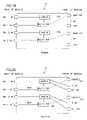
- FIG. 17is a schematic showing the normal through signal pathway through one of the circuits in the circuit module of FIG. 11 .
- FIG. 18is a schematic showing the patched signal pathway through one of the circuits in the circuit module of FIG. 11 .
- FIG. 19is another schematic showing the normal through signal pathways through the circuit module.
- FIG. 20is a schematic like FIG. 19 showing the patched signal pathways through the circuit module.
- FIG. 21is an exploded perspective view of an alternative embodiment of a connection panel including splices.
- FIG. 22is a front perspective view of another embodiment of a fiber optic connection panel with the front cover removed and a power supply module and circuit module shown in exploded form in accordance with the present invention.
- FIG. 23is a rear perspective view of the power supply module of FIG. 22 .
- FIG. 24is a front elevational view of the circuit module of FIG. 22 .
- FIG. 25is a rear elevational view of the circuit module of FIG. 22 .
- FIG. 26is a front perspective view of the circuit module of FIG. 22 .
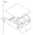
- FIG. 27is a back perspective view of the circuit module of FIG. 22 .
- FIG. 28is a perspective view of the circuit module of FIG. 22 with the cover removed.
- FIG. 29is a top view of the circuit module of FIG. 28 .
- FIG. 30is an exploded perspective view of the circuit module of FIG. 22 .
- FIG. 31is a schematic showing the normal through signal pathway through one of the circuits of the circuit module of FIG. 22 .
- FIG. 32is a schematic showing the patched signal pathway through one of the circuits of the circuit module of FIG. 22 .
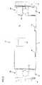
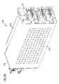
- Panel 10includes a chassis 12 with brackets 14 for mounting panel 10 to a rack, frame, cabinet, or other structure.
- Panel 10includes circuitry that connects fiber optic cables and equipment.
- the circuitryincludes a normal through state, and also a patched state for use in changing the connections between the equipment.
- the preferred circuitryalso includes monitor functions for monitoring signals through panel 10 .
- Panel 10includes a front 16 , and an opposite rear 18 .
- a top 20 , an opposite bottom 22 , a left side 24 , and a right side 26cooperate with front and back 16 , 18 to define an interior 28 for holding the circuitry.
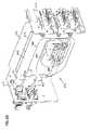
- Disposed within interior 28is a bulkhead 32 that holds a plurality of circuit modules 34 containing the circuitry.
- Panel 10includes a pivoting front cover 36 , and a pivoting rear cover 38 for allowing selective access to interior 28 through front 16 or back 18 , respectively.
- Front and rear covers 36 , 38include hinges 46 , and latches 48 for selectively latching covers 36 , 38 in the closed positions.
- Panel 10includes a front cable management arrangement 42 disposed between bulkhead 32 and front 16 . Behind bulkhead 32 , and modules 34 , panel 10 includes a rear cable management arrangement 44 . Both front and rear cable management arrangements 42 , 44 are configured for managing cables extending to and from modules 34 .
- Front cable management arrangement 42includes a plurality of front cable rings 50 . Cables extending to the fronts of modules 34 are managed by rings 50 and exit chassis 12 at openings 60 defined by the ends of front cover 36 .
- Rear cable management arrangement 44includes a plurality of rear cable rings 54 .
- Cable rings 54are used for slack storage of cables extending into chassis 12 toward modules 34 .
- Rear vertical radius limiters 52define rear openings 58 for cables entering and exiting panel 10 .
- Fan out mounts 56are also provided in rear cable management arrangement 44 for use in fanning out ribbon cables.
- rear cable management arrangement 44includes splice trays for holding cable splices.
- FIG. 21shows an alternative panel 200 including a splice tray 202 .
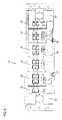
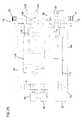
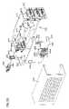
- modules 34including a module housing 62 including a first side 64 , a second side 66 , a third side 68 , and a fourth side 70 .
- a front face 72 , and an opposite rear face 74cooperate with sides 64 , 66 , 68 , 70 to define an interior 75 for holding circuit elements.
- Front face 72includes opposed flanges 76 for mounting to bulkhead 32 with fasteners 78 .
- Rear face 74 of module 34includes a plurality of termination locations or ports 80 for accessing the fiber optic circuitry contained within module housing 62 .
- each termination location 80includes a fiber optic adapter 82 .
- the illustrated adapters 82are SC type adapters.
- Each termination location in panel 10defines a port for connecting to a fiber optic cable.
- a first port 84defines a first IN port or input port.
- a second port 86defines an OUT port or output port.
- Rear face 74further includes a second IN port 88 and a second OUT port 90 .
- Rear face 74also includes a power connector 92 . In normal operation, in the normal through state, port 84 is connected to port 86 and port 88 is connected to port 90 .
- Front face 72 of module housing 62includes a first IN port 94 , and a first OUT port 96 .
- Front face 72further includes a second IN port 98 , and a second OUT port 100 .
- front ports 94 , 96 , 98 , 100are not connected to rear ports 84 , 86 , 88 , 90 .
- front port 94is connected to rear port 86 .
- front port 96is connected to rear port 84
- front port 98is connected to rear port 90
- front port 100is connected to rear port 88 .
- Front face 72further includes two monitor ports 102 , 104 for connecting to rear ports 86 , 90 , respectively.
- Switches 106 , 108 on front face 72control switching between the normal through and the patched configurations.
- First and second visual indicators 110 , 112indicate which state the switch is in.
- Switches 106 , 108are manually operated toggle switches. Other manually operated switches could be used, such as push buttons.
- Visual indicators 110 , 112are electrically powered LED's in the illustrated embodiment. The indicators are optional, since the position of the toggle switches 106 , 108 can also indicate the state of the switching circuit.
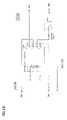
- interior 75 of module 34includes a printed circuit board 114 including fiber to PC connectors 116 and circuitry 118 .
- the fiber to PC connectors 116link ports 82 , 84 , 86 , 88 , 90 , 94 , 96 , 98 , 100 to PCB 114 .
- Circuitry 118controls operation of the circuit conditions between the normal through state and the patched state.
- Circuitry 118includes a power conversion circuit 122 for converting minus 48 VDC to plus 5 volts for operating a 2 ⁇ 2 optical switch 124 .
- Each toggle switch 106 , 108switches the respective optical switch 124 between states.
- LED's 110 , 112indicate to the operator the state of the 2 ⁇ 2 switch 124 .
- the monitor functionis carried out by a splitter 126 , such as a 90/10 splitter.
- each module 34can provide a transmit signal pathway and a receive signal pathway. Two modules 34 can be cross-connected together to cross-connect two pieces of equipment.
- Module 34includes two circuits, each with two input ports and two output ports in the normal through state and in the patched state. Module 34 can also be packaged each with a single circuit, if desired. By packaging two circuits in one module, a single 2 ⁇ 2 optical switch can be used to control the circuit states. In single circuit modules, a 1 ⁇ 2 switch would be needed for each module. With the dual circuit module, fewer switches are needed for the overall system.
- module 34can be provided with pigtails which extend out from the interior of the module through an opening 204 in the module and connect to fiber optic cables, such as through a splice in a splice tray of the panel 200 (see FIG. 21 ).
- Splice trays 202can be used in rear cable management arrangement 44 , instead of the noted cable clips and fan out mounts as shown in FIG. 21 .
- Panel 300includes many components that are similar to those described above for panel 10 .
- panel 300includes a chassis 312 with brackets 314 for mounting panel 300 to a rack, frame, cabinet, or other structure.
- Panel 300also includes an interior 328 for holding a plurality of circuit modules 334 (a single module 334 is shown in FIG. 22 ) containing circuitry, and a power supply module 336 .
- Interior 328includes rail guides 329 sized to accept fins 335 a of modules 334 , 336 to guide modules 334 , 336 into chassis 312 .
- Modules 334 , 336also include similar fins 335 b extending in an opposite direction to engage opposing rail guides (not shown) in interior 328 .
- Interior 328also includes a plurality of cable management structures including fingers 395 radius limiters 391 .
- Interior 328also includes a power bus 350 and an electrical isolation wall 351 .
- Electrical isolation wall 351 and chassis 312define therebetween a space through which electrical wires can be run to carry power from a rear of chassis 312 to connector 346 , described further below.
- Electrical isolation wall 351functions to isolate the electrical wires running therethrough from the remaining components in interior 328 .
- power supply module 336includes a front face 338 with a switch 339 that is used to turn the power supply module 336 on and off.
- a rear face 340 of the power supply module 336includes a power connector 342 and a PCB connector 344 .
- Connector 346is, in turn, connected to a source of power such as, for example, an alternating current (AC) power source.
- ACalternating current
- PCB connector 344 of power supply module 336connects to connector 348 of bus 350 mounted in interior 328 of panel 300 .
- Bus 350also includes a plurality of connectors 352 positioned along the bus 350 to provide power to modules 334 , as described below. In this configuration, power is provided from an AC source through connector 346 to power supply module 336 , and power supply module 336 provides power (e.g., 48 VDC) to connectors 352 of bus 350 through PCB connector 344 and connector 348 .
- power supply module 340is accessible from a front 302 of panel 300 .
- power supply module 340can be inserted into and removed from interior 328 of panel 300 from the front 302 of panel 300 .
- power supply module 340is “hot swappable,” meaning that power supply module 340 can be removed and/or inserted into panel 300 without turning off the AC power source to panel 300 .
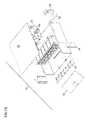
- example module 334is shown including a module housing 362 with a front face 372 and an opposite rear face 374 .
- Module housing 362also includes a sidewall 373 and a cover 376 .
- Front and rear faces 372 , 374 , sidewall 374 , and cover 376together define an interior space interior 375 for circuit elements. More or fewer walls can also be used to form interior 375 .
- Rear face 374 of module 334includes a plurality of termination locations or ports 380 for accessing the fiber optic circuitry contained within module housing 362 .
- Each termination location 380includes a fiber optic adapter 382 coupled to module 334 using a bracket 383 . See FIG. 30 .
- Bracket 383includes a tab 383 a that can be accessed (depressed) from an outside of module 334 to allow bracket 383 , adapter 382 , and an associated fiber optic connector, such as connector 462 (described further below), to be removed from termination location 380 .
- a first port 384defines a first source “S” port or input port.
- a second port 386defines a destination “D” port or output port.
- Rear face 374further includes a second source port 388 and a second destination port 390 . In normal operation, in the normal through state, port 384 is connected to port 386 and port 388 is connected to port 390 . See FIG. 31 .
- Rear face 374also includes a PCB connector 392 extending through an aperture 498 .
- PCB connector 392connects to a respective one of the connectors 352 of bus 350 and power for module 334 is provided therethrough.
- a bracket 393 coupled to rear face 374includes portions 393 a , 393 b , and 393 c that extend from rear face 374 to protect PCB connector 392 . (See also bracket 341 coupled to power supply module 336 .)
- portions 393 a , 393 b , and 393 csurround three sides of PCB connector 392 and extend beyond an end 392 a of PCB connector 392 to protect PCB connector 392 .
- Portions 393 a , 393 b , 393 care also configured so that portions 393 a , 393 b , 393 c do not interfere when PCB connector 392 is connected to connector 352 on bus 350 .
- Front face 372 of module housing 362includes a first source “S” port 394 , and a first destination “D” port 396 .
- Front face 372further includes a second source port 398 , and a second destination port 400 .
- front ports 394 , 396 , 398 , 400are not connected to rear ports 384 , 386 , 388 , 390 . See FIG. 31 .
- front port 394is connected to rear port 386 .
- front port 396is connected to rear port 384
- front port 398is connected to rear port 390
- front port 400is connected to rear port 388 . See FIG. 32 .
- Front face 372further includes two monitor ports 402 , 404 for connecting to rear ports 386 , 390 , respectively.
- Switches 406 , 408 on front face 372control switching between the normal through and the patched configurations.
- First and second visual indicators 410 , 412indicate which state each switch is in (for example, green for normal through, red for patched).
- Switches 406 , 408are manually operated toggle switches. In the example shown, switches 406 , 408 are momentary toggle switches. Other switches can be used, such as push buttons.
- Visual indicators 410 , 412are electrically powered LED's in the illustrated embodiment.
- interior 375 of module 334includes a PCB 414 coupled to sidewall 373 by screws inserted into mounts 494 of sidewall 373 .
- PCB 414includes circuitry including optical switches 424 , 426 . Each switch 406 , 408 on front face 372 switches the respective optical switch 424 , 426 between states. LED's 410 , 412 indicate the state of each switch 424 , 426 .
- PCB 414also includes PCB connector 392 extending through aperture 498 of rear face 374 to provide power to PCB 414 and switches 424 , 426 . In the example shown, PCB connector 392 is part of PCB 414 .
- PCB connector 392includes tracings that extend from PCB 414 to adjacent an end 392 a of PCB connector 392 so that, when PCB connector 392 is connected to one of the connectors 352 of bus 350 , power is provided to PCB 414 .
- a separator plate 440including legs 441 coupled to sidewall 373 by screws.
- a plurality of splitters 426 a , 426 b , 426 c , 426 dis coupled to a bracket 428 on separator plate 440 .
- splitters 426 a , 426 b , 426 c , 426 dare 90/10 splitters and perform the monitor function. In other embodiments, other splitters, such as 90/5 or 99/1 splitters, can be used.
- separator plate 440covers PCB 414 so that optical fibers in interior 375 are separated from PCB 414 , as described further below. See FIG. 30 .
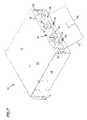
- fiber optic connectorssuch as example connectors 427 , 462
- fiber optic connectorsare connected to interior-facing ports of adapters 382 of module 334 to couple adapters 382 to switches 424 , 426 and splitters 426 a , 426 b , 426 c , 426 d , respectively.
- connector 462is connected to adapter 382 associated with source port 384 on rear face 374 .
- connectors 427 , 462are SC-type connectors, although other types of connectors such as, for example, FC, ST, and LX.5 can also be used. (The other adapters 382 are shown with dust caps connected therein.)
- Connector 462includes an optical cable 464 running from connector 462 to optical switch 424 .
- Optical switch 424is in turn connected to splitter 426 c by cable 466
- splitter 426 cis connected to fiber optic connector 427 by cable 465 to complete the normal through route.
- connectorscan be connected to each of the adapters of module 334 , and cables can be used to connect the connectors to the respective switches and splitters.
- bracket 383 , adapter 382 , and connector 462can be removed from rear face 374 (see, for example, FIG. 30 ) so that connector 462 can be accessed by removing connector 462 from adapter 382 .
- Optical cable 464is looped within interior 375 of module 334 so that slack is provided when connector 462 is removed. (Although only a single loop is shown for purposes of clarity, cable 464 can be looped multiple times to provide greater amounts of slack.) For example, in one embodiment slack in cable 464 is provided so that connector 462 can be pulled approximately six inches out of module 334 so that connector 462 can be cleaned or replaced.
- more or less slackcan be provided such as, for example, three inches, nine inches, or twelve inches.
- Cable 465is similarly provided with slack so that connector 427 can be removed. Cables connected to the other adapters can also be provided with slack.
- Separator plate 440generally functions to cover PCB 414 and manage the slack in the cables (e.g., cables 464 , 465 ) away from PCB 414 . In this manner, the slack in the cables is protected from contacting sharp edges or snagging on PCB 414 or any components mounted thereon.
- cablese.g., cables 464 , 465
- clips 470 , 472can be mounted to separator plate 440 to further manage the slack in the cables as the cables are looped within interior 375 . Further, in additional circular loops, slack in the cables can also be looped in “ Figure 8” configurations as well. These types of looping configurations allow the slack in the cables to be managed by separator plate 440 while maintaining the cables with proper bend radii.
Landscapes
- Physics & Mathematics (AREA)
- General Physics & Mathematics (AREA)
- Optics & Photonics (AREA)
- Light Guides In General And Applications Therefor (AREA)
- Mechanical Coupling Of Light Guides (AREA)
Abstract
Description
Claims (18)
Priority Applications (2)
| Application Number | Priority Date | Filing Date | Title |
|---|---|---|---|
| US11/080,141US7412147B2 (en) | 2005-03-15 | 2005-03-15 | Normal through optical panel |
| US12/171,390US7587116B2 (en) | 2005-03-15 | 2008-07-11 | Normal through optical panel |
Applications Claiming Priority (1)
| Application Number | Priority Date | Filing Date | Title |
|---|---|---|---|
| US11/080,141US7412147B2 (en) | 2005-03-15 | 2005-03-15 | Normal through optical panel |
Related Child Applications (1)
| Application Number | Title | Priority Date | Filing Date |
|---|---|---|---|
| US12/171,390ContinuationUS7587116B2 (en) | 2005-03-15 | 2008-07-11 | Normal through optical panel |
Publications (2)
| Publication Number | Publication Date |
|---|---|
| US20060210229A1 US20060210229A1 (en) | 2006-09-21 |
| US7412147B2true US7412147B2 (en) | 2008-08-12 |
Family
ID=37010435
Family Applications (2)
| Application Number | Title | Priority Date | Filing Date |
|---|---|---|---|
| US11/080,141Expired - Fee RelatedUS7412147B2 (en) | 2005-03-15 | 2005-03-15 | Normal through optical panel |
| US12/171,390Expired - LifetimeUS7587116B2 (en) | 2005-03-15 | 2008-07-11 | Normal through optical panel |
Family Applications After (1)
| Application Number | Title | Priority Date | Filing Date |
|---|---|---|---|
| US12/171,390Expired - LifetimeUS7587116B2 (en) | 2005-03-15 | 2008-07-11 | Normal through optical panel |
Country Status (1)
| Country | Link |
|---|---|
| US (2) | US7412147B2 (en) |
Cited By (16)
| Publication number | Priority date | Publication date | Assignee | Title |
|---|---|---|---|---|
| US20080267574A1 (en)* | 2005-03-15 | 2008-10-30 | Adc Telecommunications, Inc. | Normal Through Optical Panel |
| US8958679B2 (en) | 2010-03-02 | 2015-02-17 | Tyco Electronics Services Gmbh | Fibre-optic telecommunications module |
| US9146374B2 (en) | 2012-09-28 | 2015-09-29 | Adc Telecommunications, Inc. | Rapid deployment packaging for optical fiber |
| US9223094B2 (en) | 2012-10-05 | 2015-12-29 | Tyco Electronics Nederland Bv | Flexible optical circuit, cassettes, and methods |
| US9335484B2 (en) | 2013-03-15 | 2016-05-10 | Commscope Technologies Llc | Passive optical through switches |
| US9435975B2 (en) | 2013-03-15 | 2016-09-06 | Commscope Technologies Llc | Modular high density telecommunications frame and chassis system |
| US9494758B2 (en) | 2014-04-03 | 2016-11-15 | Commscope Technologies Llc | Fiber optic distribution system |
| US9535229B2 (en) | 2011-10-07 | 2017-01-03 | Commscope Technologies Llc | Fiber optic cassette, system, and method |
| US9851524B2 (en) | 2014-01-28 | 2017-12-26 | Commscope Technologies Llc | Slidable fiber optic connection module with cable slack management |
| US10416406B1 (en) | 2018-03-01 | 2019-09-17 | Afl Telecommunications Llc | Communications module housing |
| US10451828B1 (en) | 2018-11-09 | 2019-10-22 | Afl Telecommunications Llc | Communications module housing |
| US11372165B2 (en) | 2011-09-12 | 2022-06-28 | Commscope Technologies Llc | Flexible lensed optical interconnect device for signal distribution |
| US11409068B2 (en) | 2017-10-02 | 2022-08-09 | Commscope Technologies Llc | Fiber optic circuit and preparation method |
| US11592628B2 (en) | 2012-09-28 | 2023-02-28 | Commscope Technologies Llc | Fiber optic cassette |
| US12158613B2 (en) | 2022-02-02 | 2024-12-03 | Sanwa Technologies, Inc. | Optical connector switches, systems, and methods |
| US12339511B2 (en) | 2020-03-31 | 2025-06-24 | Commscope Technologies Llc | Fiber optic cable management systems and methods |
Families Citing this family (26)
| Publication number | Priority date | Publication date | Assignee | Title |
|---|---|---|---|---|
| US7376321B2 (en)* | 2004-08-09 | 2008-05-20 | Adc Telecommunications, Inc. | Modules including multiple rows of adapters for high density optical fiber distribution frame |
| US8798427B2 (en) | 2007-09-05 | 2014-08-05 | Corning Cable Systems Llc | Fiber optic terminal assembly |
| CN101983364B (en)* | 2008-01-31 | 2013-01-16 | 惠普开发有限公司 | Modular data processing components and systems |
| US8249410B2 (en)* | 2008-04-25 | 2012-08-21 | Corning Cable Systems Llc | Connector housing for a communication network |
| CN102209921B (en) | 2008-10-09 | 2015-11-25 | 康宁光缆系统有限公司 | There is the fibre-optic terminus supported from the adapter panel of the input and output optical fiber of optical splitters |
| US8879882B2 (en) | 2008-10-27 | 2014-11-04 | Corning Cable Systems Llc | Variably configurable and modular local convergence point |
| WO2010059623A1 (en) | 2008-11-21 | 2010-05-27 | Adc Telecommunications, Inc. | Fiber optic telecommunications module |
| US20100129030A1 (en)* | 2008-11-24 | 2010-05-27 | Giraud William J | Universal Optical Splitter Modules and Related Mounting Brackets, Assemblies and Methods |
| ATE535833T1 (en) | 2009-05-23 | 2011-12-15 | Ccs Technology Inc | CONNECTOR HOUSING FOR A RADIO OVER FIBER OPTICAL CABLE SYSTEM |
| JP5330140B2 (en)* | 2009-07-29 | 2013-10-30 | 日本オクラロ株式会社 | Optical module |
| WO2011100613A1 (en)* | 2010-02-12 | 2011-08-18 | Adc Telecommunications, Inc. | Communications bladed system |
| US9547144B2 (en) | 2010-03-16 | 2017-01-17 | Corning Optical Communications LLC | Fiber optic distribution network for multiple dwelling units |
| US8792767B2 (en) | 2010-04-16 | 2014-07-29 | Ccs Technology, Inc. | Distribution device |
| WO2012054454A2 (en) | 2010-10-19 | 2012-04-26 | Corning Cable Systems Llc | Transition box for multiple dwelling unit fiber optic distribution network |
| US9219546B2 (en) | 2011-12-12 | 2015-12-22 | Corning Optical Communications LLC | Extremely high frequency (EHF) distributed antenna systems, and related components and methods |
| US8995136B2 (en) | 2011-12-23 | 2015-03-31 | Adc Telecommunications, Inc. | Communications bladed panel systems |
| US10110307B2 (en) | 2012-03-02 | 2018-10-23 | Corning Optical Communications LLC | Optical network units (ONUs) for high bandwidth connectivity, and related components and methods |
| US9004778B2 (en) | 2012-06-29 | 2015-04-14 | Corning Cable Systems Llc | Indexable optical fiber connectors and optical fiber connector arrays |
| US9049500B2 (en) | 2012-08-31 | 2015-06-02 | Corning Cable Systems Llc | Fiber optic terminals, systems, and methods for network service management |
| US8909019B2 (en) | 2012-10-11 | 2014-12-09 | Ccs Technology, Inc. | System comprising a plurality of distribution devices and distribution device |
| CH707427A1 (en)* | 2012-12-31 | 2014-07-15 | Illi Sys | Junction box for optical waveguide. |
| AU2015308577A1 (en)* | 2014-08-29 | 2017-03-30 | Corning Optical Communications LLC | Fiber optic solutions for migration between duplex and parallel multi-fiber solutions |
| US9525483B2 (en)* | 2015-03-17 | 2016-12-20 | Verizon Patent And Licensing Inc. | Actively monitored optical fiber panel |
| US20220196921A1 (en)* | 2020-12-17 | 2022-06-23 | Panduit Corp. | Method and apparatus for blocking the transmission of classified data over optical fiber |
| JP7457206B2 (en)* | 2021-04-23 | 2024-03-27 | 株式会社フジクラ | optical termination box |
| CN116520519B (en)* | 2023-04-07 | 2024-03-19 | 合肥比洋通信科技有限公司 | OXC all-optical backboard |
Citations (21)
| Publication number | Priority date | Publication date | Assignee | Title |
|---|---|---|---|---|
| US3668476A (en) | 1970-09-11 | 1972-06-06 | Seeburg Corp | Self-locking enclosure for electronic circuitry and method of assembling the same |
| US5189410A (en) | 1989-12-28 | 1993-02-23 | Fujitsu Limited | Digital cross connect system |
| US5363465A (en) | 1993-02-19 | 1994-11-08 | Adc Telecommunications, Inc. | Fiber optic connector module |
| US5432875A (en) | 1993-02-19 | 1995-07-11 | Adc Telecommunications, Inc. | Fiber optic monitor module |
| US5627925A (en) | 1995-04-07 | 1997-05-06 | Lucent Technologies Inc. | Non-blocking optical cross-connect structure for telecommunications network |
| EP0828356A2 (en) | 1996-09-09 | 1998-03-11 | Lucent Technologies Inc. | Optical monitoring and test access interconnection module |
| US5943461A (en)* | 1997-05-12 | 1999-08-24 | Lucent Technologies Inc | Connectorized optical module package and method using same with internal fiber connections |
| US6208796B1 (en) | 1998-07-21 | 2001-03-27 | Adc Telecommunications, Inc. | Fiber optic module |
| US6226111B1 (en) | 1996-12-06 | 2001-05-01 | Telcordia Technologies, Inc. | Inter-ring cross-connect for survivable multi-wavelength optical communication networks |
| US6263136B1 (en)* | 1999-10-29 | 2001-07-17 | Lucent Technologies | Intelligent optical transmitter module |
| US6363183B1 (en) | 2000-01-04 | 2002-03-26 | Seungug Koh | Reconfigurable and scalable intergrated optic waveguide add/drop multiplexing element using micro-opto-electro-mechanical systems and methods of fabricating thereof |
| US6370294B1 (en) | 1999-06-25 | 2002-04-09 | Adc Telecommunications, Inc. | Fiber optic circuit and module with switch |
| US6418262B1 (en) | 2000-03-13 | 2002-07-09 | Adc Telecommunications, Inc. | Fiber distribution frame with fiber termination blocks |
| US20020181896A1 (en) | 2001-06-04 | 2002-12-05 | Mcclellan Brian J. | Telecommunications chassis and module |
| US6614953B2 (en) | 2001-03-16 | 2003-09-02 | Photuris, Inc. | Modular all-optical cross-connect |
| US20030210882A1 (en)* | 2002-04-19 | 2003-11-13 | Barthel William F. | Optical fiber management system and method |
| US6668108B1 (en) | 2000-06-02 | 2003-12-23 | Calient Networks, Inc. | Optical cross-connect switch with integrated optical signal tap |
| US20040161207A1 (en)* | 2001-04-14 | 2004-08-19 | Chiu Liew C. | Fiber optic modules with de-latching mechanism |
| US6795632B1 (en)* | 2001-11-02 | 2004-09-21 | Ciena Corporation | System for managing slack in fiber optic cables connected to a circuit board |
| US20050232565A1 (en)* | 2004-04-16 | 2005-10-20 | Ross Heggestad | Normal through optical panel |
| US20060093302A1 (en)* | 2004-11-03 | 2006-05-04 | James Solheid | Optical fiber slack storage tray for distribution cabinet |
Family Cites Families (7)
| Publication number | Priority date | Publication date | Assignee | Title |
|---|---|---|---|---|
| US4820007A (en)* | 1988-02-12 | 1989-04-11 | American Telephone And Telegraph Company At&T Bell Laboratories | Cable closure and methods of assembling |
| US5214444A (en)* | 1991-09-19 | 1993-05-25 | Eastman Kodak Company | Optical fiber mount and support |
| IT1255953B (en)* | 1992-10-30 | 1995-11-17 | Pirelli Cavi Spa | COMPACT OPTICAL AMPLIFIER WITH SEPARATE FUNCTIONS |
| DE4430512C2 (en)* | 1994-08-27 | 2000-06-29 | Bosch Gmbh Robert | Device for connecting a reinforcing fiber |
| US6396990B1 (en)* | 1998-06-12 | 2002-05-28 | Netrix Technologies, Inc. | Multi-purpose communications cabinet |
| US7366416B2 (en)* | 2003-08-11 | 2008-04-29 | General Instrument Corporation | Hub for a passive optical network hub |
| US7412147B2 (en)* | 2005-03-15 | 2008-08-12 | Adc Telecommunications, Inc. | Normal through optical panel |
- 2005
- 2005-03-15USUS11/080,141patent/US7412147B2/ennot_activeExpired - Fee Related
- 2008
- 2008-07-11USUS12/171,390patent/US7587116B2/ennot_activeExpired - Lifetime
Patent Citations (22)
| Publication number | Priority date | Publication date | Assignee | Title |
|---|---|---|---|---|
| US3668476A (en) | 1970-09-11 | 1972-06-06 | Seeburg Corp | Self-locking enclosure for electronic circuitry and method of assembling the same |
| US5189410A (en) | 1989-12-28 | 1993-02-23 | Fujitsu Limited | Digital cross connect system |
| US5363465A (en) | 1993-02-19 | 1994-11-08 | Adc Telecommunications, Inc. | Fiber optic connector module |
| US5432875A (en) | 1993-02-19 | 1995-07-11 | Adc Telecommunications, Inc. | Fiber optic monitor module |
| US5627925A (en) | 1995-04-07 | 1997-05-06 | Lucent Technologies Inc. | Non-blocking optical cross-connect structure for telecommunications network |
| EP0828356A2 (en) | 1996-09-09 | 1998-03-11 | Lucent Technologies Inc. | Optical monitoring and test access interconnection module |
| US6226111B1 (en) | 1996-12-06 | 2001-05-01 | Telcordia Technologies, Inc. | Inter-ring cross-connect for survivable multi-wavelength optical communication networks |
| US5943461A (en)* | 1997-05-12 | 1999-08-24 | Lucent Technologies Inc | Connectorized optical module package and method using same with internal fiber connections |
| US6208796B1 (en) | 1998-07-21 | 2001-03-27 | Adc Telecommunications, Inc. | Fiber optic module |
| US6556738B2 (en)* | 1999-06-25 | 2003-04-29 | Alcon Technologies, Inc. | Fiber optic circuit and module with switch |
| US6370294B1 (en) | 1999-06-25 | 2002-04-09 | Adc Telecommunications, Inc. | Fiber optic circuit and module with switch |
| US6263136B1 (en)* | 1999-10-29 | 2001-07-17 | Lucent Technologies | Intelligent optical transmitter module |
| US6363183B1 (en) | 2000-01-04 | 2002-03-26 | Seungug Koh | Reconfigurable and scalable intergrated optic waveguide add/drop multiplexing element using micro-opto-electro-mechanical systems and methods of fabricating thereof |
| US6418262B1 (en) | 2000-03-13 | 2002-07-09 | Adc Telecommunications, Inc. | Fiber distribution frame with fiber termination blocks |
| US6668108B1 (en) | 2000-06-02 | 2003-12-23 | Calient Networks, Inc. | Optical cross-connect switch with integrated optical signal tap |
| US6614953B2 (en) | 2001-03-16 | 2003-09-02 | Photuris, Inc. | Modular all-optical cross-connect |
| US20040161207A1 (en)* | 2001-04-14 | 2004-08-19 | Chiu Liew C. | Fiber optic modules with de-latching mechanism |
| US20020181896A1 (en) | 2001-06-04 | 2002-12-05 | Mcclellan Brian J. | Telecommunications chassis and module |
| US6795632B1 (en)* | 2001-11-02 | 2004-09-21 | Ciena Corporation | System for managing slack in fiber optic cables connected to a circuit board |
| US20030210882A1 (en)* | 2002-04-19 | 2003-11-13 | Barthel William F. | Optical fiber management system and method |
| US20050232565A1 (en)* | 2004-04-16 | 2005-10-20 | Ross Heggestad | Normal through optical panel |
| US20060093302A1 (en)* | 2004-11-03 | 2006-05-04 | James Solheid | Optical fiber slack storage tray for distribution cabinet |
Non-Patent Citations (1)
| Title |
|---|
| U.S. Appl. No. 10/826,152, filed Apr. 16, 2004, 29 pages. |
Cited By (40)
| Publication number | Priority date | Publication date | Assignee | Title |
|---|---|---|---|---|
| US7587116B2 (en)* | 2005-03-15 | 2009-09-08 | Adc Telecommunications, Inc. | Normal through optical panel |
| US20080267574A1 (en)* | 2005-03-15 | 2008-10-30 | Adc Telecommunications, Inc. | Normal Through Optical Panel |
| US8958679B2 (en) | 2010-03-02 | 2015-02-17 | Tyco Electronics Services Gmbh | Fibre-optic telecommunications module |
| US11372165B2 (en) | 2011-09-12 | 2022-06-28 | Commscope Technologies Llc | Flexible lensed optical interconnect device for signal distribution |
| US9535229B2 (en) | 2011-10-07 | 2017-01-03 | Commscope Technologies Llc | Fiber optic cassette, system, and method |
| US11061197B2 (en) | 2011-10-07 | 2021-07-13 | Commscope Technologies Llc | Fiber optic cassette, system, and method |
| US10578821B2 (en) | 2011-10-07 | 2020-03-03 | Commscope Technologies Llc | Fiber optic cassette, system, and method |
| US9952400B2 (en) | 2011-10-07 | 2018-04-24 | Commscope Technologies Llc | Fiber optic cassette, system, and method |
| US11561356B2 (en) | 2011-10-07 | 2023-01-24 | Commscope Technologies Llc | Fiber optic cassette, system, and method |
| US9146374B2 (en) | 2012-09-28 | 2015-09-29 | Adc Telecommunications, Inc. | Rapid deployment packaging for optical fiber |
| US9470869B2 (en) | 2012-09-28 | 2016-10-18 | Commscope Technologies Llc | Rapid deployment packaging for optical fiber |
| US11592628B2 (en) | 2012-09-28 | 2023-02-28 | Commscope Technologies Llc | Fiber optic cassette |
| US9927591B2 (en) | 2012-09-28 | 2018-03-27 | Commscope Technologies Llc | Rapid deployment packaging for optical fiber |
| US11573389B2 (en) | 2012-10-05 | 2023-02-07 | Commscope Asia Holdings B.V. | Flexible optical circuit, cassettes, and methods |
| US9874711B2 (en) | 2012-10-05 | 2018-01-23 | Commscope Asia Holdings B.V. | Flexible optical circuit, cassettes, and methods |
| US12130487B2 (en) | 2012-10-05 | 2024-10-29 | Commscope Asia Holdings B.V. | Flexible optical circuit, cassettes, and methods |
| US10955633B2 (en) | 2012-10-05 | 2021-03-23 | Commscope Asia Holdings B.V. | Flexible optical circuit, cassettes, and methods |
| US10317638B2 (en) | 2012-10-05 | 2019-06-11 | Commscope Asia Holdings B.V. | Flexible optical circuit, cassettes, and methods |
| US9223094B2 (en) | 2012-10-05 | 2015-12-29 | Tyco Electronics Nederland Bv | Flexible optical circuit, cassettes, and methods |
| US10473875B2 (en) | 2013-03-15 | 2019-11-12 | Commscope Technologies Llc | Modular high density telecommunications frame and chassis system |
| US9772450B2 (en) | 2013-03-15 | 2017-09-26 | Commscope Technologies Llc | Passive optical through switches |
| US9335484B2 (en) | 2013-03-15 | 2016-05-10 | Commscope Technologies Llc | Passive optical through switches |
| US9435975B2 (en) | 2013-03-15 | 2016-09-06 | Commscope Technologies Llc | Modular high density telecommunications frame and chassis system |
| US9952398B2 (en) | 2013-03-15 | 2018-04-24 | Commscope Technologies Llc | Modular high density telecommunications frame and chassis system |
| US10545307B2 (en) | 2014-01-28 | 2020-01-28 | Commscope Technologies Llc | Slidable fiber optic connection module with cable slack management |
| US11733472B2 (en) | 2014-01-28 | 2023-08-22 | Commscope Technologies Llc | Slidable fiber optic connection module with cable slack management |
| US11249270B2 (en) | 2014-01-28 | 2022-02-15 | Commscope Technologies Llc | Slidable fiber optic connection module with cable slack management |
| US9851524B2 (en) | 2014-01-28 | 2017-12-26 | Commscope Technologies Llc | Slidable fiber optic connection module with cable slack management |
| US10481357B2 (en) | 2014-04-03 | 2019-11-19 | Commscope Technologies Llc | Fiber optic distribution system |
| US9977212B2 (en) | 2014-04-03 | 2018-05-22 | Commscope Technologies Llc | Fiber optic distribution system |
| US9494758B2 (en) | 2014-04-03 | 2016-11-15 | Commscope Technologies Llc | Fiber optic distribution system |
| US11409068B2 (en) | 2017-10-02 | 2022-08-09 | Commscope Technologies Llc | Fiber optic circuit and preparation method |
| US11609400B2 (en) | 2017-10-02 | 2023-03-21 | Commscope Technologies Llc | Fiber optic circuit and preparation method |
| US12276858B2 (en) | 2017-10-02 | 2025-04-15 | Commscope Technologies Llc | Fiber optic circuit and preparation method |
| US10823927B2 (en) | 2018-03-01 | 2020-11-03 | Afl Telecommunications Llc | Communications module housing |
| US10416406B1 (en) | 2018-03-01 | 2019-09-17 | Afl Telecommunications Llc | Communications module housing |
| US10451828B1 (en) | 2018-11-09 | 2019-10-22 | Afl Telecommunications Llc | Communications module housing |
| US10802235B2 (en) | 2018-11-09 | 2020-10-13 | Afl Telecommunications Llc | Communications module housing |
| US12339511B2 (en) | 2020-03-31 | 2025-06-24 | Commscope Technologies Llc | Fiber optic cable management systems and methods |
| US12158613B2 (en) | 2022-02-02 | 2024-12-03 | Sanwa Technologies, Inc. | Optical connector switches, systems, and methods |
Also Published As
| Publication number | Publication date |
|---|---|
| US7587116B2 (en) | 2009-09-08 |
| US20060210229A1 (en) | 2006-09-21 |
| US20080267574A1 (en) | 2008-10-30 |
Similar Documents
| Publication | Publication Date | Title |
|---|---|---|
| US7412147B2 (en) | Normal through optical panel | |
| US20050232565A1 (en) | Normal through optical panel | |
| US7577331B2 (en) | Optical fiber coupler module | |
| US20170192191A1 (en) | Fiber optic solutions for migration between duplex and parallel multi-fiber solutions allowing for full fiber utilization | |
| US7809234B2 (en) | Telecommunications cabinet with connector storage | |
| CA2799225C (en) | Fiber optic cable management module and panel | |
| US6359789B1 (en) | Heterogeneous functions-integrated communication device | |
| CA2780576C (en) | Optical backplane rack assembly with external optical connectors | |
| JP4614864B2 (en) | Communication equipment | |
| CN217133439U (en) | Optical fiber junction box and optical fiber case comprising same | |
| CN216561114U (en) | Cap type optical fiber connector box | |
| CN215867246U (en) | Optical cable fiber-dividing box | |
| JP2012008289A (en) | Optical line housing structure | |
| HK1238723A1 (en) | Fiber optic solutions for migration between duplex and parallel multi-fiber solutions |
Legal Events
| Date | Code | Title | Description |
|---|---|---|---|
| AS | Assignment | Owner name:ADC TELECOMMUNICATIONS, INC., MINNESOTA Free format text:ASSIGNMENT OF ASSIGNORS INTEREST;ASSIGNOR:SCADDEN, JARROD CHARLES;REEL/FRAME:016389/0889 Effective date:20050315 | |
| STCF | Information on status: patent grant | Free format text:PATENTED CASE | |
| CC | Certificate of correction | ||
| FPAY | Fee payment | Year of fee payment:4 | |
| AS | Assignment | Owner name:TYCO ELECTRONICS SERVICES GMBH, SWITZERLAND Free format text:ASSIGNMENT OF ASSIGNORS INTEREST;ASSIGNOR:ADC TELECOMMUNICATIONS, INC.;REEL/FRAME:036060/0174 Effective date:20110930 | |
| AS | Assignment | Owner name:COMMSCOPE EMEA LIMITED, IRELAND Free format text:ASSIGNMENT OF ASSIGNORS INTEREST;ASSIGNOR:TYCO ELECTRONICS SERVICES GMBH;REEL/FRAME:036956/0001 Effective date:20150828 | |
| AS | Assignment | Owner name:COMMSCOPE TECHNOLOGIES LLC, NORTH CAROLINA Free format text:ASSIGNMENT OF ASSIGNORS INTEREST;ASSIGNOR:COMMSCOPE EMEA LIMITED;REEL/FRAME:037012/0001 Effective date:20150828 | |
| AS | Assignment | Owner name:JPMORGAN CHASE BANK, N.A., AS COLLATERAL AGENT, ILLINOIS Free format text:PATENT SECURITY AGREEMENT (TERM);ASSIGNOR:COMMSCOPE TECHNOLOGIES LLC;REEL/FRAME:037513/0709 Effective date:20151220 Owner name:JPMORGAN CHASE BANK, N.A., AS COLLATERAL AGENT, ILLINOIS Free format text:PATENT SECURITY AGREEMENT (ABL);ASSIGNOR:COMMSCOPE TECHNOLOGIES LLC;REEL/FRAME:037514/0196 Effective date:20151220 Owner name:JPMORGAN CHASE BANK, N.A., AS COLLATERAL AGENT, IL Free format text:PATENT SECURITY AGREEMENT (ABL);ASSIGNOR:COMMSCOPE TECHNOLOGIES LLC;REEL/FRAME:037514/0196 Effective date:20151220 Owner name:JPMORGAN CHASE BANK, N.A., AS COLLATERAL AGENT, IL Free format text:PATENT SECURITY AGREEMENT (TERM);ASSIGNOR:COMMSCOPE TECHNOLOGIES LLC;REEL/FRAME:037513/0709 Effective date:20151220 | |
| FPAY | Fee payment | Year of fee payment:8 | |
| AS | Assignment | Owner name:ANDREW LLC, NORTH CAROLINA Free format text:RELEASE BY SECURED PARTY;ASSIGNOR:JPMORGAN CHASE BANK, N.A.;REEL/FRAME:048840/0001 Effective date:20190404 Owner name:ALLEN TELECOM LLC, ILLINOIS Free format text:RELEASE BY SECURED PARTY;ASSIGNOR:JPMORGAN CHASE BANK, N.A.;REEL/FRAME:048840/0001 Effective date:20190404 Owner name:REDWOOD SYSTEMS, INC., NORTH CAROLINA Free format text:RELEASE BY SECURED PARTY;ASSIGNOR:JPMORGAN CHASE BANK, N.A.;REEL/FRAME:048840/0001 Effective date:20190404 Owner name:COMMSCOPE TECHNOLOGIES LLC, NORTH CAROLINA Free format text:RELEASE BY SECURED PARTY;ASSIGNOR:JPMORGAN CHASE BANK, N.A.;REEL/FRAME:048840/0001 Effective date:20190404 Owner name:COMMSCOPE, INC. OF NORTH CAROLINA, NORTH CAROLINA Free format text:RELEASE BY SECURED PARTY;ASSIGNOR:JPMORGAN CHASE BANK, N.A.;REEL/FRAME:048840/0001 Effective date:20190404 Owner name:COMMSCOPE, INC. OF NORTH CAROLINA, NORTH CAROLINA Free format text:RELEASE BY SECURED PARTY;ASSIGNOR:JPMORGAN CHASE BANK, N.A.;REEL/FRAME:049260/0001 Effective date:20190404 Owner name:COMMSCOPE TECHNOLOGIES LLC, NORTH CAROLINA Free format text:RELEASE BY SECURED PARTY;ASSIGNOR:JPMORGAN CHASE BANK, N.A.;REEL/FRAME:049260/0001 Effective date:20190404 Owner name:ALLEN TELECOM LLC, ILLINOIS Free format text:RELEASE BY SECURED PARTY;ASSIGNOR:JPMORGAN CHASE BANK, N.A.;REEL/FRAME:049260/0001 Effective date:20190404 Owner name:ANDREW LLC, NORTH CAROLINA Free format text:RELEASE BY SECURED PARTY;ASSIGNOR:JPMORGAN CHASE BANK, N.A.;REEL/FRAME:049260/0001 Effective date:20190404 Owner name:REDWOOD SYSTEMS, INC., NORTH CAROLINA Free format text:RELEASE BY SECURED PARTY;ASSIGNOR:JPMORGAN CHASE BANK, N.A.;REEL/FRAME:049260/0001 Effective date:20190404 | |
| AS | Assignment | Owner name:JPMORGAN CHASE BANK, N.A., NEW YORK Free format text:ABL SECURITY AGREEMENT;ASSIGNORS:COMMSCOPE, INC. OF NORTH CAROLINA;COMMSCOPE TECHNOLOGIES LLC;ARRIS ENTERPRISES LLC;AND OTHERS;REEL/FRAME:049892/0396 Effective date:20190404 Owner name:WILMINGTON TRUST, NATIONAL ASSOCIATION, AS COLLATE Free format text:PATENT SECURITY AGREEMENT;ASSIGNOR:COMMSCOPE TECHNOLOGIES LLC;REEL/FRAME:049892/0051 Effective date:20190404 Owner name:JPMORGAN CHASE BANK, N.A., NEW YORK Free format text:TERM LOAN SECURITY AGREEMENT;ASSIGNORS:COMMSCOPE, INC. OF NORTH CAROLINA;COMMSCOPE TECHNOLOGIES LLC;ARRIS ENTERPRISES LLC;AND OTHERS;REEL/FRAME:049905/0504 Effective date:20190404 Owner name:WILMINGTON TRUST, NATIONAL ASSOCIATION, AS COLLATERAL AGENT, CONNECTICUT Free format text:PATENT SECURITY AGREEMENT;ASSIGNOR:COMMSCOPE TECHNOLOGIES LLC;REEL/FRAME:049892/0051 Effective date:20190404 | |
| FEPP | Fee payment procedure | Free format text:MAINTENANCE FEE REMINDER MAILED (ORIGINAL EVENT CODE: REM.); ENTITY STATUS OF PATENT OWNER: LARGE ENTITY | |
| LAPS | Lapse for failure to pay maintenance fees | Free format text:PATENT EXPIRED FOR FAILURE TO PAY MAINTENANCE FEES (ORIGINAL EVENT CODE: EXP.); ENTITY STATUS OF PATENT OWNER: LARGE ENTITY | |
| STCH | Information on status: patent discontinuation | Free format text:PATENT EXPIRED DUE TO NONPAYMENT OF MAINTENANCE FEES UNDER 37 CFR 1.362 | |
| FP | Lapsed due to failure to pay maintenance fee | Effective date:20200812 | |
| AS | Assignment | Owner name:BISON PATENT LICENSING, LLC, GEORGIA Free format text:ASSIGNMENT OF ASSIGNORS INTEREST;ASSIGNOR:COMMSCOPE TECHNOLOGIES LLC;REEL/FRAME:060641/0312 Effective date:20220628 | |
| AS | Assignment | Owner name:RUCKUS WIRELESS, LLC (F/K/A RUCKUS WIRELESS, INC.), NORTH CAROLINA Free format text:RELEASE OF SECURITY INTEREST AT REEL/FRAME 049905/0504;ASSIGNOR:JPMORGAN CHASE BANK, N.A., AS COLLATERAL AGENT;REEL/FRAME:071477/0255 Effective date:20241217 Owner name:COMMSCOPE TECHNOLOGIES LLC, NORTH CAROLINA Free format text:RELEASE OF SECURITY INTEREST AT REEL/FRAME 049905/0504;ASSIGNOR:JPMORGAN CHASE BANK, N.A., AS COLLATERAL AGENT;REEL/FRAME:071477/0255 Effective date:20241217 Owner name:COMMSCOPE, INC. OF NORTH CAROLINA, NORTH CAROLINA Free format text:RELEASE OF SECURITY INTEREST AT REEL/FRAME 049905/0504;ASSIGNOR:JPMORGAN CHASE BANK, N.A., AS COLLATERAL AGENT;REEL/FRAME:071477/0255 Effective date:20241217 Owner name:ARRIS SOLUTIONS, INC., NORTH CAROLINA Free format text:RELEASE OF SECURITY INTEREST AT REEL/FRAME 049905/0504;ASSIGNOR:JPMORGAN CHASE BANK, N.A., AS COLLATERAL AGENT;REEL/FRAME:071477/0255 Effective date:20241217 Owner name:ARRIS TECHNOLOGY, INC., NORTH CAROLINA Free format text:RELEASE OF SECURITY INTEREST AT REEL/FRAME 049905/0504;ASSIGNOR:JPMORGAN CHASE BANK, N.A., AS COLLATERAL AGENT;REEL/FRAME:071477/0255 Effective date:20241217 Owner name:ARRIS ENTERPRISES LLC (F/K/A ARRIS ENTERPRISES, INC.), NORTH CAROLINA Free format text:RELEASE OF SECURITY INTEREST AT REEL/FRAME 049905/0504;ASSIGNOR:JPMORGAN CHASE BANK, N.A., AS COLLATERAL AGENT;REEL/FRAME:071477/0255 Effective date:20241217 |