US7411281B2 - Integrated circuit device package having both wire bond and flip-chip interconnections and method of making the same - Google Patents
Integrated circuit device package having both wire bond and flip-chip interconnections and method of making the sameDownload PDFInfo
- Publication number
- US7411281B2 US7411281B2US10/870,928US87092804AUS7411281B2US 7411281 B2US7411281 B2US 7411281B2US 87092804 AUS87092804 AUS 87092804AUS 7411281 B2US7411281 B2US 7411281B2
- Authority
- US
- United States
- Prior art keywords
- die
- interposer
- array
- electrically conductive
- device package
- Prior art date
- Legal status (The legal status is an assumption and is not a legal conclusion. Google has not performed a legal analysis and makes no representation as to the accuracy of the status listed.)
- Expired - Fee Related
Links
Images


Classifications
- H—ELECTRICITY
- H01—ELECTRIC ELEMENTS
- H01L—SEMICONDUCTOR DEVICES NOT COVERED BY CLASS H10
- H01L23/00—Details of semiconductor or other solid state devices
- H01L23/34—Arrangements for cooling, heating, ventilating or temperature compensation ; Temperature sensing arrangements
- H01L23/36—Selection of materials, or shaping, to facilitate cooling or heating, e.g. heatsinks
- H—ELECTRICITY
- H01—ELECTRIC ELEMENTS
- H01L—SEMICONDUCTOR DEVICES NOT COVERED BY CLASS H10
- H01L23/00—Details of semiconductor or other solid state devices
- H01L23/28—Encapsulations, e.g. encapsulating layers, coatings, e.g. for protection
- H01L23/31—Encapsulations, e.g. encapsulating layers, coatings, e.g. for protection characterised by the arrangement or shape
- H01L23/3107—Encapsulations, e.g. encapsulating layers, coatings, e.g. for protection characterised by the arrangement or shape the device being completely enclosed
- H01L23/3121—Encapsulations, e.g. encapsulating layers, coatings, e.g. for protection characterised by the arrangement or shape the device being completely enclosed a substrate forming part of the encapsulation
- H01L23/3128—Encapsulations, e.g. encapsulating layers, coatings, e.g. for protection characterised by the arrangement or shape the device being completely enclosed a substrate forming part of the encapsulation the substrate having spherical bumps for external connection
- H—ELECTRICITY
- H01—ELECTRIC ELEMENTS
- H01L—SEMICONDUCTOR DEVICES NOT COVERED BY CLASS H10
- H01L23/00—Details of semiconductor or other solid state devices
- H01L23/48—Arrangements for conducting electric current to or from the solid state body in operation, e.g. leads, terminal arrangements ; Selection of materials therefor
- H01L23/488—Arrangements for conducting electric current to or from the solid state body in operation, e.g. leads, terminal arrangements ; Selection of materials therefor consisting of soldered or bonded constructions
- H01L23/498—Leads, i.e. metallisations or lead-frames on insulating substrates, e.g. chip carriers
- H01L23/49811—Additional leads joined to the metallisation on the insulating substrate, e.g. pins, bumps, wires, flat leads
- H01L23/49816—Spherical bumps on the substrate for external connection, e.g. ball grid arrays [BGA]
- H—ELECTRICITY
- H01—ELECTRIC ELEMENTS
- H01L—SEMICONDUCTOR DEVICES NOT COVERED BY CLASS H10
- H01L23/00—Details of semiconductor or other solid state devices
- H01L23/48—Arrangements for conducting electric current to or from the solid state body in operation, e.g. leads, terminal arrangements ; Selection of materials therefor
- H01L23/488—Arrangements for conducting electric current to or from the solid state body in operation, e.g. leads, terminal arrangements ; Selection of materials therefor consisting of soldered or bonded constructions
- H01L23/498—Leads, i.e. metallisations or lead-frames on insulating substrates, e.g. chip carriers
- H01L23/49833—Leads, i.e. metallisations or lead-frames on insulating substrates, e.g. chip carriers the chip support structure consisting of a plurality of insulating substrates
- H—ELECTRICITY
- H01—ELECTRIC ELEMENTS
- H01L—SEMICONDUCTOR DEVICES NOT COVERED BY CLASS H10
- H01L2224/00—Indexing scheme for arrangements for connecting or disconnecting semiconductor or solid-state bodies and methods related thereto as covered by H01L24/00
- H01L2224/01—Means for bonding being attached to, or being formed on, the surface to be connected, e.g. chip-to-package, die-attach, "first-level" interconnects; Manufacturing methods related thereto
- H01L2224/10—Bump connectors; Manufacturing methods related thereto
- H01L2224/15—Structure, shape, material or disposition of the bump connectors after the connecting process
- H01L2224/16—Structure, shape, material or disposition of the bump connectors after the connecting process of an individual bump connector
- H01L2224/161—Disposition
- H01L2224/16151—Disposition the bump connector connecting between a semiconductor or solid-state body and an item not being a semiconductor or solid-state body, e.g. chip-to-substrate, chip-to-passive
- H01L2224/16221—Disposition the bump connector connecting between a semiconductor or solid-state body and an item not being a semiconductor or solid-state body, e.g. chip-to-substrate, chip-to-passive the body and the item being stacked
- H01L2224/16225—Disposition the bump connector connecting between a semiconductor or solid-state body and an item not being a semiconductor or solid-state body, e.g. chip-to-substrate, chip-to-passive the body and the item being stacked the item being non-metallic, e.g. insulating substrate with or without metallisation
- H—ELECTRICITY
- H01—ELECTRIC ELEMENTS
- H01L—SEMICONDUCTOR DEVICES NOT COVERED BY CLASS H10
- H01L2224/00—Indexing scheme for arrangements for connecting or disconnecting semiconductor or solid-state bodies and methods related thereto as covered by H01L24/00
- H01L2224/01—Means for bonding being attached to, or being formed on, the surface to be connected, e.g. chip-to-package, die-attach, "first-level" interconnects; Manufacturing methods related thereto
- H01L2224/26—Layer connectors, e.g. plate connectors, solder or adhesive layers; Manufacturing methods related thereto
- H01L2224/31—Structure, shape, material or disposition of the layer connectors after the connecting process
- H01L2224/32—Structure, shape, material or disposition of the layer connectors after the connecting process of an individual layer connector
- H01L2224/321—Disposition
- H01L2224/32151—Disposition the layer connector connecting between a semiconductor or solid-state body and an item not being a semiconductor or solid-state body, e.g. chip-to-substrate, chip-to-passive
- H01L2224/32221—Disposition the layer connector connecting between a semiconductor or solid-state body and an item not being a semiconductor or solid-state body, e.g. chip-to-substrate, chip-to-passive the body and the item being stacked
- H01L2224/32225—Disposition the layer connector connecting between a semiconductor or solid-state body and an item not being a semiconductor or solid-state body, e.g. chip-to-substrate, chip-to-passive the body and the item being stacked the item being non-metallic, e.g. insulating substrate with or without metallisation
- H—ELECTRICITY
- H01—ELECTRIC ELEMENTS
- H01L—SEMICONDUCTOR DEVICES NOT COVERED BY CLASS H10
- H01L2224/00—Indexing scheme for arrangements for connecting or disconnecting semiconductor or solid-state bodies and methods related thereto as covered by H01L24/00
- H01L2224/01—Means for bonding being attached to, or being formed on, the surface to be connected, e.g. chip-to-package, die-attach, "first-level" interconnects; Manufacturing methods related thereto
- H01L2224/26—Layer connectors, e.g. plate connectors, solder or adhesive layers; Manufacturing methods related thereto
- H01L2224/31—Structure, shape, material or disposition of the layer connectors after the connecting process
- H01L2224/32—Structure, shape, material or disposition of the layer connectors after the connecting process of an individual layer connector
- H01L2224/321—Disposition
- H01L2224/32151—Disposition the layer connector connecting between a semiconductor or solid-state body and an item not being a semiconductor or solid-state body, e.g. chip-to-substrate, chip-to-passive
- H01L2224/32221—Disposition the layer connector connecting between a semiconductor or solid-state body and an item not being a semiconductor or solid-state body, e.g. chip-to-substrate, chip-to-passive the body and the item being stacked
- H01L2224/32245—Disposition the layer connector connecting between a semiconductor or solid-state body and an item not being a semiconductor or solid-state body, e.g. chip-to-substrate, chip-to-passive the body and the item being stacked the item being metallic
- H—ELECTRICITY
- H01—ELECTRIC ELEMENTS
- H01L—SEMICONDUCTOR DEVICES NOT COVERED BY CLASS H10
- H01L2224/00—Indexing scheme for arrangements for connecting or disconnecting semiconductor or solid-state bodies and methods related thereto as covered by H01L24/00
- H01L2224/01—Means for bonding being attached to, or being formed on, the surface to be connected, e.g. chip-to-package, die-attach, "first-level" interconnects; Manufacturing methods related thereto
- H01L2224/42—Wire connectors; Manufacturing methods related thereto
- H01L2224/47—Structure, shape, material or disposition of the wire connectors after the connecting process
- H01L2224/48—Structure, shape, material or disposition of the wire connectors after the connecting process of an individual wire connector
- H01L2224/4805—Shape
- H01L2224/4809—Loop shape
- H01L2224/48091—Arched
- H—ELECTRICITY
- H01—ELECTRIC ELEMENTS
- H01L—SEMICONDUCTOR DEVICES NOT COVERED BY CLASS H10
- H01L2224/00—Indexing scheme for arrangements for connecting or disconnecting semiconductor or solid-state bodies and methods related thereto as covered by H01L24/00
- H01L2224/01—Means for bonding being attached to, or being formed on, the surface to be connected, e.g. chip-to-package, die-attach, "first-level" interconnects; Manufacturing methods related thereto
- H01L2224/42—Wire connectors; Manufacturing methods related thereto
- H01L2224/47—Structure, shape, material or disposition of the wire connectors after the connecting process
- H01L2224/48—Structure, shape, material or disposition of the wire connectors after the connecting process of an individual wire connector
- H01L2224/481—Disposition
- H01L2224/48151—Connecting between a semiconductor or solid-state body and an item not being a semiconductor or solid-state body, e.g. chip-to-substrate, chip-to-passive
- H01L2224/48221—Connecting between a semiconductor or solid-state body and an item not being a semiconductor or solid-state body, e.g. chip-to-substrate, chip-to-passive the body and the item being stacked
- H01L2224/48225—Connecting between a semiconductor or solid-state body and an item not being a semiconductor or solid-state body, e.g. chip-to-substrate, chip-to-passive the body and the item being stacked the item being non-metallic, e.g. insulating substrate with or without metallisation
- H01L2224/48227—Connecting between a semiconductor or solid-state body and an item not being a semiconductor or solid-state body, e.g. chip-to-substrate, chip-to-passive the body and the item being stacked the item being non-metallic, e.g. insulating substrate with or without metallisation connecting the wire to a bond pad of the item
- H—ELECTRICITY
- H01—ELECTRIC ELEMENTS
- H01L—SEMICONDUCTOR DEVICES NOT COVERED BY CLASS H10
- H01L2224/00—Indexing scheme for arrangements for connecting or disconnecting semiconductor or solid-state bodies and methods related thereto as covered by H01L24/00
- H01L2224/73—Means for bonding being of different types provided for in two or more of groups H01L2224/10, H01L2224/18, H01L2224/26, H01L2224/34, H01L2224/42, H01L2224/50, H01L2224/63, H01L2224/71
- H01L2224/732—Location after the connecting process
- H01L2224/73201—Location after the connecting process on the same surface
- H01L2224/73203—Bump and layer connectors
- H01L2224/73204—Bump and layer connectors the bump connector being embedded into the layer connector
- H—ELECTRICITY
- H01—ELECTRIC ELEMENTS
- H01L—SEMICONDUCTOR DEVICES NOT COVERED BY CLASS H10
- H01L2224/00—Indexing scheme for arrangements for connecting or disconnecting semiconductor or solid-state bodies and methods related thereto as covered by H01L24/00
- H01L2224/73—Means for bonding being of different types provided for in two or more of groups H01L2224/10, H01L2224/18, H01L2224/26, H01L2224/34, H01L2224/42, H01L2224/50, H01L2224/63, H01L2224/71
- H01L2224/732—Location after the connecting process
- H01L2224/73201—Location after the connecting process on the same surface
- H01L2224/73207—Bump and wire connectors
- H—ELECTRICITY
- H01—ELECTRIC ELEMENTS
- H01L—SEMICONDUCTOR DEVICES NOT COVERED BY CLASS H10
- H01L2224/00—Indexing scheme for arrangements for connecting or disconnecting semiconductor or solid-state bodies and methods related thereto as covered by H01L24/00
- H01L2224/73—Means for bonding being of different types provided for in two or more of groups H01L2224/10, H01L2224/18, H01L2224/26, H01L2224/34, H01L2224/42, H01L2224/50, H01L2224/63, H01L2224/71
- H01L2224/732—Location after the connecting process
- H01L2224/73251—Location after the connecting process on different surfaces
- H01L2224/73265—Layer and wire connectors
- H—ELECTRICITY
- H01—ELECTRIC ELEMENTS
- H01L—SEMICONDUCTOR DEVICES NOT COVERED BY CLASS H10
- H01L24/00—Arrangements for connecting or disconnecting semiconductor or solid-state bodies; Methods or apparatus related thereto
- H01L24/01—Means for bonding being attached to, or being formed on, the surface to be connected, e.g. chip-to-package, die-attach, "first-level" interconnects; Manufacturing methods related thereto
- H01L24/42—Wire connectors; Manufacturing methods related thereto
- H01L24/47—Structure, shape, material or disposition of the wire connectors after the connecting process
- H01L24/48—Structure, shape, material or disposition of the wire connectors after the connecting process of an individual wire connector
- H—ELECTRICITY
- H01—ELECTRIC ELEMENTS
- H01L—SEMICONDUCTOR DEVICES NOT COVERED BY CLASS H10
- H01L24/00—Arrangements for connecting or disconnecting semiconductor or solid-state bodies; Methods or apparatus related thereto
- H01L24/73—Means for bonding being of different types provided for in two or more of groups H01L24/10, H01L24/18, H01L24/26, H01L24/34, H01L24/42, H01L24/50, H01L24/63, H01L24/71
- H—ELECTRICITY
- H01—ELECTRIC ELEMENTS
- H01L—SEMICONDUCTOR DEVICES NOT COVERED BY CLASS H10
- H01L2924/00—Indexing scheme for arrangements or methods for connecting or disconnecting semiconductor or solid-state bodies as covered by H01L24/00
- H01L2924/0001—Technical content checked by a classifier
- H01L2924/00014—Technical content checked by a classifier the subject-matter covered by the group, the symbol of which is combined with the symbol of this group, being disclosed without further technical details
- H—ELECTRICITY
- H01—ELECTRIC ELEMENTS
- H01L—SEMICONDUCTOR DEVICES NOT COVERED BY CLASS H10
- H01L2924/00—Indexing scheme for arrangements or methods for connecting or disconnecting semiconductor or solid-state bodies as covered by H01L24/00
- H01L2924/01—Chemical elements
- H01L2924/01078—Platinum [Pt]
- H—ELECTRICITY
- H01—ELECTRIC ELEMENTS
- H01L—SEMICONDUCTOR DEVICES NOT COVERED BY CLASS H10
- H01L2924/00—Indexing scheme for arrangements or methods for connecting or disconnecting semiconductor or solid-state bodies as covered by H01L24/00
- H01L2924/01—Chemical elements
- H01L2924/01079—Gold [Au]
- H—ELECTRICITY
- H01—ELECTRIC ELEMENTS
- H01L—SEMICONDUCTOR DEVICES NOT COVERED BY CLASS H10
- H01L2924/00—Indexing scheme for arrangements or methods for connecting or disconnecting semiconductor or solid-state bodies as covered by H01L24/00
- H01L2924/10—Details of semiconductor or other solid state devices to be connected
- H01L2924/11—Device type
- H01L2924/14—Integrated circuits
- H—ELECTRICITY
- H01—ELECTRIC ELEMENTS
- H01L—SEMICONDUCTOR DEVICES NOT COVERED BY CLASS H10
- H01L2924/00—Indexing scheme for arrangements or methods for connecting or disconnecting semiconductor or solid-state bodies as covered by H01L24/00
- H01L2924/15—Details of package parts other than the semiconductor or other solid state devices to be connected
- H01L2924/151—Die mounting substrate
- H01L2924/1515—Shape
- H01L2924/15153—Shape the die mounting substrate comprising a recess for hosting the device
- H—ELECTRICITY
- H01—ELECTRIC ELEMENTS
- H01L—SEMICONDUCTOR DEVICES NOT COVERED BY CLASS H10
- H01L2924/00—Indexing scheme for arrangements or methods for connecting or disconnecting semiconductor or solid-state bodies as covered by H01L24/00
- H01L2924/15—Details of package parts other than the semiconductor or other solid state devices to be connected
- H01L2924/151—Die mounting substrate
- H01L2924/15165—Monolayer substrate
- H—ELECTRICITY
- H01—ELECTRIC ELEMENTS
- H01L—SEMICONDUCTOR DEVICES NOT COVERED BY CLASS H10
- H01L2924/00—Indexing scheme for arrangements or methods for connecting or disconnecting semiconductor or solid-state bodies as covered by H01L24/00
- H01L2924/15—Details of package parts other than the semiconductor or other solid state devices to be connected
- H01L2924/151—Die mounting substrate
- H01L2924/153—Connection portion
- H01L2924/1531—Connection portion the connection portion being formed only on the surface of the substrate opposite to the die mounting surface
- H01L2924/15311—Connection portion the connection portion being formed only on the surface of the substrate opposite to the die mounting surface being a ball array, e.g. BGA
- H—ELECTRICITY
- H01—ELECTRIC ELEMENTS
- H01L—SEMICONDUCTOR DEVICES NOT COVERED BY CLASS H10
- H01L2924/00—Indexing scheme for arrangements or methods for connecting or disconnecting semiconductor or solid-state bodies as covered by H01L24/00
- H01L2924/15—Details of package parts other than the semiconductor or other solid state devices to be connected
- H01L2924/151—Die mounting substrate
- H01L2924/153—Connection portion
- H01L2924/1532—Connection portion the connection portion being formed on the die mounting surface of the substrate
- H01L2924/15321—Connection portion the connection portion being formed on the die mounting surface of the substrate being a ball array, e.g. BGA
Definitions
- the inventionrelates generally to the field of integrated circuit (IC) device packaging technology and, more particularly to IC device packages with enhanced thermal, electrical, and input/output (I/O) properties.
- ICintegrated circuit
- An array IC device packageincludes a plurality of electrically conductive terminals (e.g., solder balls, pins, pads, etc.) arranged in an array (i.e., columns and rows) on a bottom surface of a package substrate. Signals from an IC die mounted on a surface of the substrate are routed through the substrate to the electrically conductive terminals on the bottom surface. The electrically conductive terminals are configured to be attached to the PCB.
- Example array IC device packagesinclude ball grid array (BGA), pin grid array (PGA), and land grid array (LGA) packages.
- Array IC device packagescan have die-up and die-down configurations.
- the IC dieIn die-up packages, the IC die is mounted on a top surface of the substrate, opposite the surface to which the electrically conductive terminals are attached.
- die-down packagesthe IC die is mounted on the bottom surface of the substrate, on the same surface where the electrically conductive terminals are located.
- the present inventionis directed to integrated circuit (IC) device packages that provide enhanced thermal, electrical, and input/output (I/O) performance, and methods for making the same.
- ICintegrated circuit
- IC device packagesare described herein having an IC die coupled to a substrate with at least one wire bond, and an interposer coupled to the IC die in a flip-chip fashion.
- Example embodiments of the present inventionare described below.
- a die-down array IC device packageincludes a heat spreader having a first surface with a central cavity formed therein.
- the packagefurther includes a substrate having a first surface coupled to the first surface of the heat spreader.
- An array of electrically conductive terminalsis coupled to a second surface of the substrate.
- a central opening through the substrateoverlaps the central cavity.
- the packagefurther includes an IC die, which has a first surface mounted to the first surface of the heat spreader, within the central cavity. At least one wire bond couples at least one bond pad on a second surface of the IC die to at least one bond pad on the second surface of the substrate.
- the packagefurther includes an interposer. A plurality of electrically conductive bumps on the second surface of the IC die is coupled to corresponding bond pads on a first surface of the interposer.
- the die-down array IC device packageincludes an underfill material that fills a space between the IC die and the interposer, and an encapsulating material that encapsulates the IC die and the at least one wire bond.
- the die-down array IC device packageincludes a heat slug coupled to a second surface of the interposer.
- the heat spreaderin another embodiment, includes a substantially planar body having opposing first and second surfaces, and a ring-shaped body having a central opening that is open at first and second surfaces of the ring-shaped body.
- the first surface of the ring-shaped bodyis coupled to the first surface of the substantially planar body.
- the second surfaces of the ring-shaped body and the substantially planar bodyform the first and second surfaces, respectively, of the heat spreader.
- the central opening through the ring-shaped body and a portion of the first surface of the substantially planar body that is exposed through the central openingform the central cavity.
- a method of making a die-down array IC device packageincludes the step of coupling a first surface of a substrate to a first surface of a heat spreader. The method further includes the step of mounting a first surface of an IC die to the first surface of the heat spreader, within a central cavity formed in the first surface of the heat spreader. The method further includes the step of coupling a plurality of bond pads on a second surface of the IC die to corresponding bond pads on a second surface of the substrate with a plurality of wire bonds.
- the methodfurther includes the step of coupling a first surface of an interposer to the second surface of the IC die so that a plurality of electrically conductive bumps on the second surface of the IC die is coupled to corresponding bond pads on the first surface of the interposer.
- the methodfurther includes the steps of filling a space between the IC die and the interposer with an underfill material, and encapsulating the IC die and the plurality of wire bonds with an encapsulating material.
- the methodfurther includes the step of coupling a heat slug to a second surface the interposer.
- the methodincludes the step of coupling a first surface of a ring-shaped body to a first surface of a substantially planar body to form the heat spreader. Second surfaces of the ring-shaped body and the substantially planar body form the first and second surfaces of said heat spreader, respectively.
- the central opening through the substrateoverlaps a central opening through the ring-shaped body that is open at the first and second surfaces of the ring-shaped body.
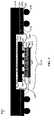
- FIG. 1Aillustrates a cross-sectional view of a conventional die-down BGA package with wire bond interconnections.
- FIG. 1Billustrates a cross-sectional view of a conventional die-up BGA package with flip-chip interconnections.
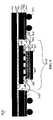
- FIG. 2Aillustrates a cross-sectional view of a die-down BGA package, having an interposer attached to a flip-chip mounted IC die, in accordance with an example embodiment of the present invention.
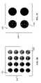
- FIGS. 2B and 2Cillustrate top and bottom views, respectively, of the interposer illustrated in FIG. 2A , in accordance with an example embodiment of the present invention.
- FIG. 2Dillustrates the die-down BGA package shown in FIG. 2A , having an underfill material between the interposer and the IC die, in accordance with an example embodiment of the present invention.
- FIG. 3illustrates a cross-sectional view of a die-down BGA package, having an interposer attached to a flip-chip mounted IC die and a heat slug attached to the interposer, in accordance with an example embodiment of the present invention.
- FIG. 4illustrates a cross-sectional view of a die-down BGA package, having a two-piece heat spreader, and an interposer attached to a flip-chip mounted IC die, in accordance with an example embodiment of the present invention.
- FIG. 5illustrates a cross-sectional view of a die-down BGA package, having a two-piece heat spreader, an interposer attached to a flip-chip mounted IC die, and a heat slug attached to the interposer, in accordance with an example embodiment of the present invention.
- FIGS. 6-9 , 10 A, and 10 Bshow flowcharts providing example steps for assembling die-down array IC device packages with enhanced thermal, electrical, and/or input/output (I/O) performance, in accordance with example embodiments of the present invention.
- Some conventional array integrated circuit (IC) device packageshave wire bond interconnections to couple signals of the IC die from corresponding bond pads on the active surface of the IC die to the package substrate.
- Other conventional array IC device packageshave flip-chip interconnections to couple signals of the IC die from an array of conductive bumps on the active surface of the IC die to the package substrate.
- the package substratehas internal routing that electrically couples the signals of the IC die to an array of electrically conductive terminals on a bottom surface of the substrate, and the package is typically mounted to a printed circuit board (PCB).
- PCBprinted circuit board
- thermal performanceis limited because there is no direct thermal path from the active surface of the IC die to the PCB.
- Electrical performanceis also limited because there is no direct electrical path for routing signals from the center of the IC die to the PCB.
- signals routed from the center of the IC dietraverse a longer electrical path than signals routed from an edge.
- Relatively short electrical pathsare desirable because they introduce less resistance than relatively long electrical paths. Signals traversing relatively long electrical paths can experience significant drops in potential due to the increased resistance.
- an active surface of the IC diehas at least one bond pad for wire bond interconnections to a package substrate, in addition to at least one electrically conductive bump for flip-chip interconnection to an interposer.
- the substrate and the interposerare configured to be coupled to a PCB.
- enhanced thermal propertiesare present due to a direct thermal path from the active surface of the IC die to the PCB, through the interposer.
- enhanced electrical propertiesare present due to a direct electrical path from the active surface of the IC die to the PCB, through the interposer. Additionally, because both wire bond pads and flip-chip bumps are used to interconnect signals, more I/O connections can be achieved compared to conventional IC device packages having either wire bond or flip-chip interconnections alone.
- FIG. 1Aillustrates a cross-sectional view of a conventional die-down ball grid array (BGA) package 100 .
- BGA package 100includes an IC die 105 , a die attach adhesive 125 , a heat spreader 110 , and a package substrate 120 .
- BGA package 100further includes a plurality of wire bonds 115 , a plurality of solder balls 130 , and an encapsulating material 135 .
- IC die 105is mounted to heat spreader 110 in a die-down configuration with die attach adhesive 125 .
- a first surface of substrate 120is attached to heat spreader 110 .
- Wire bonds 115couple signals of IC die 105 to a second surface of substrate 120 .
- Solder balls 130are attached to the second surface of substrate 120 .
- Solder balls 130are reflowed to attach BGA package 100 to a PCB (not shown in FIG. 1A ).
- a thermal pathis present in BGA package 100 from the active surface of IC die 105 to the PCB through encapsulating material 135 .
- typical encapsulating materials 135lack thermal conductivity.
- an indirect thermal pathis present from the active surface of IC die 105 to the PCB through adhesive 125 , heat spreader 110 , substrate 120 , and solder balls 130 .
- BGA package 100provides limited thermal performance because there is no direct thermally conductive path from the active surface of IC die 105 to the PCB.
- BGA package 100also provides limited electrical performance. For example, routing signals from the center of IC die 105 to substrate 120 with wire bonds 115 introduces increased resistance because wire bonds 115 increase in length with distance from the edge of IC die 105 . The increased resistance introduced by the longer electrical paths results in an undesirable drop in signal potential.
- FIG. 1Billustrates a cross-sectional view of a conventional die-up BGA package 150 .
- BGA package 150includes an IC die 155 , a package substrate 160 , a plurality of electrically conductive bumps 170 , a plurality of solder balls 175 , and an underfill material 165 .
- IC die 155is mounted to a first surface of substrate 160 in a die-up configuration. Electrically conductive bumps 170 of an active surface of IC die 155 are coupled to conductive pads on the first surface of substrate 160 . Electrically conductive bumps 170 couple signals in IC die 155 to substrate 160 .
- Underfill material 165is applied between the active surface of IC die 155 and the first surface of substrate 160 .
- Solder balls 175are attached to a second surface of substrate 160 . Solder balls 175 are reflowed to attach BGA package 150 to a PCB (not shown in FIG. 1B ).
- BGA package 150provides limited I/O performance because a high-density substrate 160 with numerous routing layers would be needed to effectively route a large number of signals from the array of conductive pads on the first surface of substrate 160 , to which IC die 155 is mounted. Numerous routing layers are undesirable because the cost of substrate 160 typically increases with the number of routing layers. In some cases (e.g., when the flip-chip bump pitch is extremely dense), it is not be possible with current technology to manufacture a substrate 160 having a high enough density.
- FIG. 2Aillustrates a cross-sectional view of a die-down BGA package 200 , in accordance with an embodiment of the present invention.
- BGA package 200includes an IC die 205 , a die attach material 215 , a heat spreader 210 with a central cavity 255 formed therein, a package substrate 220 , and an interposer 240 .
- BGA package 200further includes an encapsulating material 260 , a plurality of wire bonds 230 , a plurality of corresponding bond pads 225 , a plurality of electrically conductive bumps 235 , a plurality of solder balls 245 , and a plurality of solder balls 250 .
- a first surface 211 of heat spreader 210has central cavity 255 formed therein.
- Substrate 220has a central opening 223 that is open at a first surface 221 and a second surface 222 of substrate 220 .
- First surface 221 of substrate 220is coupled to first surface 211 of heat spreader 210 .
- Central opening 223 through substrate 220overlaps central cavity 255 formed in heat spreader 210 .
- IC die 205is mounted in a die-down configuration with die attach adhesive 215 to first surface 211 in cavity 255 of heat spreader 210 .
- Solder balls 245are coupled to second surface 222 of substrate 220 .
- Bond pads 225are located on a peripheral area of an active surface 202 of IC die 205 .
- Wire bonds 230connect bond pads 225 to second surface 222 of substrate 220 (e.g., to traces, contacts, ground rings, ground planes, voltage planes, etc. of substrate 220 ).
- Bond pads 225can be any type of signal pads of IC die 205 , including I/O pads, voltage pads, ground pads, test pads, etc.
- Electrically conductive bumps 235are located on a central area of active surface 202 of IC die 205 , and are arranged in any configuration, including an array (i.e., in columns and rows). Electrically conductive bumps 235 are flip-chip coupled to corresponding bond pads (not shown in FIG. 2A ) on a first surface 241 of interposer 240 . Solder balls 250 are coupled to a second surface 242 of interposer 240 .
- FIGS. 2B and 2Cillustrate example bond pad 236 and solder ball 250 configurations on first and second surfaces 241 and 242 of interposer 240 , respectively, for BGA package 200 shown in FIG. 2A , according to an example embodiment of the present invention. It is noted that any number of bond pads 236 and solder balls 250 may be present in interposer 240 , as is desired for the particular implementation.
- Solder balls 245 and 250are reflowed to attach BGA package 200 to a PCB.
- Solder balls 245 and 250can be implemented with other types of electrically conductive terminals (e.g., pins, studs, other kinds of balls, etc.).
- An encapsulating material 260encapsulates IC die 205 and wire bonds 230 .
- an underfill material 265fills a space between active surface 202 of IC die 205 and first surface 241 of interposer 240 .
- Underfill material 265is typically applied before encapsulating material 260 , but can also be applied after encapsulating material 260 is applied.
- Example materials for underfill material 265include conventional underfill materials, including silicon oxide, or any other kind of underfill material.
- Underfill material 265is typically different from encapsulating material 260 but, in some cases, underfill material 265 and encapsulating material 260 can be the same material.
- Example materials for heat spreader 210include copper, aluminum, aluminum based alloys, copper based alloys, ferromagnetic materials, laminated copper/iron, other metals and combinations of metals/alloys, other thermally and/or electrically conductive materials (e.g., ceramics, metallized plastics, etc.), and other materials described elsewhere herein. Machining, etching, stamping, and other techniques can be used to form central cavity 255 in first surface 211 of heat spreader 210 .
- Example materials for die attach adhesive 215include epoxy, such as a silver epoxy, solder, and other adhesive materials.
- Example materials for substrate 220include tape, laminate, ceramic, organic (e.g., BT, FR4, etc.), and other materials.
- Substrate 220can have one or more electrical routing layers, which can be constructed through lamination, build-up, or other processes.
- Substrate 220can further include single or multi-layer electrical conductive traces or planes.
- Example materials for electrically conductive bumps 235include lead/tin solder, gold, gold/tin, other metal or metal composites, electrically conductive epoxy, and other electrically conductive materials.
- Example materials for interposer 240include tape, metal, a substrate (e.g., laminate or ceramic), an IC, or any combination of these materials (e.g., tape with metal stiffener, tape with laminate or ceramic substrate, IC with metal slug, etc). Reflow process, thermal compression, thermal sonic bonding, and other methods can be used to attach interposer 240 .
- Interposer 240can be attached either before wafer dice or singulation (i.e., when IC die 205 is in wafer form) or after IC die 205 has been singulated, including when it is attached to heat spreader 210 .
- BGA package 200includes both wire bond 230 and flip-chip 235 interconnections in the same package. Accordingly, BGA package 200 significantly increases the number of I/O signals that can be routed to and from IC die 205 , without reducing the minimum pitch of I/O pads on IC die 205 or requiring substrate 220 be high-density. Additionally, BGA package 200 has enhanced thermal properties due to the more direct thermal path from active surface 202 of IC die 205 to the PCB, through interposer 240 . BGA package 200 also has enhanced electrical properties due to the more direct electrical path from IC die 205 to the PCB, through interposer 240 .
- FIG. 3illustrates a cross-sectional view of a die-down BGA package 300 , in accordance with an embodiment of the present invention.
- BGA package 300is similar to BGA package 200 , shown in FIG. 2A , except a heat slug 305 replaces solder balls 250 for additional thermal enhancement.
- Heat slug 305has a first surface 306 coupled to second surface 242 of interposer 240 .
- Heat slug 305has a second surface 307 , which is configured to be surface mounted to a PCB.
- Example materials for heat slug 305include copper, aluminum, other metals or combinations of metals/alloys, ceramics, and other thermally and/or electrically conductive materials.
- heat slug 305is formed separately and then attached to interposer 240 .
- heat slug 305is formed by depositing a plating layer on second surface 242 of interposer 240 . Heat slug 305 can also be formed in other ways.
- BGA package 300is configured without a separate heat slug 305 .
- interposer 240incorporates the function of heat slug 305 , and second surface 242 of interposer 240 is configured to be mounted to the PCB.
- BGA package 300a single electrical signal can be routed from IC die 205 to the PCB through heat slug 305 . Accordingly, BGA package 300 is advantageous for routing a single power, ground, or other signal of IC die 205 to the PCB, through interposer 240 and heat slug 305 .
- BGA package 200shown in FIG. 2A , is advantageous for routing multiple I/O signals from IC die 205 , through the center of the package, to the PCB. Because BGA package 200 has solder balls 250 instead of heat slug 305 (shown in FIG. 3 ), multiple I/O signals can be routed from IC die 205 to the PCB, through interposer 240 and solder balls 250 . Accordingly, BGA package 200 provides a direct electrical path for routing critical I/O signals with less resistance and therefore little drop in signal potential.
- FIG. 4illustrates a cross-sectional view of a die-down BGA package 400 .
- BGA package 400is similar to BGA package 200 , shown in FIG. 2A , except that package 400 includes a two-piece heat spreader formed from a planar heat spreader 410 and a ring-shaped body 420 .
- BGA package 400includes IC die 205 , planar heat spreader 410 , adhesive material 215 , ring-shaped body 420 , substrate 220 , and interposer 240 .
- BGA package 400further includes plurality of wire bonds 230 , plurality of corresponding bond pads 225 , plurality of electrically conductive bumps 235 , plurality of solder balls 245 , and plurality of solder balls 250 .
- Elements in FIG. 4are generally similar to the corresponding elements shown in FIG. 2 , with differences described below.
- BGA package 400includes a two-piece heat spreader formed by coupling ring-shaped body 420 to planar heat spreader 410 .
- Ring-shaped body 420has a central opening that is open at a first surface 421 and a second surface 422 of ring-shaped body 420 .
- central cavity 255is formed in first surface 211 of heat spreader 210 .
- central cavity 255is formed by coupling first surface 421 of ring-shaped body 420 to a first surface 411 of planar heat spreader 410 with adhesive material 215 .
- First surface 221 of substrate 220is coupled to second surface 422 of ring-shaped body 420 .
- IC die 205is mounted with adhesive material 215 in a die-down configuration to first surface 411 of heat spreader 410 , within central cavity 255 .
- Solder balls 245are coupled to second surface 222 of substrate 220 .
- Example materials for heat spreader 410 and ring-shaped body 420include copper, aluminum, aluminum based alloys, copper based alloys, ferromagnetic materials, laminated copper/iron, other metals and combinations of metals/alloys, other thermally and/or electrically conductive materials (e.g., ceramics, metallized plastics, etc.), and other materials described elsewhere herein.
- Heat spreader 410 and ring-shaped body 420are typically made from the same material (e.g., to match coefficients of thermal expansion (CTE)), but can be made from different materials.
- CTEcoefficients of thermal expansion
- BGA package 400like BGA package 200 , described above, includes both wire bond 230 and flip-chip 235 interconnections in the same package. Therefore, BGA package 400 significantly increases the number of I/O signals that can be routed to and from IC die 205 , without reducing the minimum pitch of I/O pads on IC die 205 or requiring substrate 220 be high-density. Additionally, BGA package 400 has enhanced thermal properties due to the more direct thermal path from active surface 202 of IC die 205 to the PCB, through interposer 240 . BGA package 400 also has enhanced electrical properties due to the more direct electrical path from IC die 205 to the PCB, through interposer 240 .
- FIG. 5illustrates a cross-sectional view of a die-down BGA package 500 .
- BGA package 500is similar to BGA package 400 of FIG. 4 , except heat slug 305 replaces solder balls 250 for additional thermal enhancement, similarly to BGA package 300 shown in FIG. 3 .
- First surface 306 of heat slug 305is coupled to second surface 242 of interposer 240 .
- Second surface 307 of heat slug 305is configured to be mounted to a PCB.
- BGA package 500is configured without a separate heat slug 305 .
- interposer 240incorporates the function of heat slug 305 , and second surface 242 of interposer 240 is configured to be mounted to the PCB.
- FIG. 6shows flowchart 600 , providing steps for assembling an array IC device package with enhanced thermal, electrical, and/or I/O properties, according to one or more embodiments of the present invention.
- FIGS. 7-9 , 10 A, and 10 Bprovide additional optional steps, according to further embodiments of the present invention.
- the steps of FIGS. 6-9 , 10 A, and 10 Bdo not necessarily have to occur in the order shown, as will be apparent to persons skilled in the relevant art(s) based on the teachings herein.
- Other operational and structural embodimentswill be apparent to persons skilled in the relevant art(s) based on the following discussion. These steps are described in detail below.
- Flowchart 600is shown in FIG. 6 , and begins with step 605 .
- a substrateis coupled to a heat spreader.
- the substrateis substrate 220
- the heat spreaderis heat spreader 210 , as shown in FIGS. 2A and 3 .
- an IC dieis mounted to the heat spreader.
- the IC dieis mounted in a central cavity formed in the heat spreader, and the IC die is IC die 205 , the heat spreader is heat spreader 210 , the central cavity is central cavity 255 , and the substrate is substrate 220 .
- a plurality of bond pads on the IC dieare coupled to corresponding bond pads on the substrate with wire bonds.
- the IC dieis IC die 205
- the plurality of bond pads on the IC dieis plurality of bond pads 225
- the substrateis substrate 220
- the wire bondsare wire bonds 230 , as shown in FIGS. 2 A and 3 - 5 .
- an interposeris coupled to the IC die so that a plurality of electrically conductive bumps on the IC die are coupled to corresponding bond pads on the interposer.
- the IC dieis IC die 205
- the plurality of electrically conductive bumps on the IC dieis plurality of electrically conductive bumps 235
- the interposeris interposer 240 , as shown in FIGS. 2 A and 3 - 5 .
- flowchart 600includes the step shown in FIG. 7 for forming a two-piece heat spreader.
- a ring-shaped bodyis coupled to a substantially planar heat spreader to form the heat spreader described in steps 605 and 610 of FIG. 6 .
- the ring-shaped bodyis ring-shaped body 420
- the planar heat spreaderis planar heat spreader 410 , as shown in FIGS. 4 and 5 .
- flowchart 600includes one or more of the steps shown in FIG. 8 .
- step 805an array of electrically conductive terminals is formed on the substrate.
- the array of electrically conductive terminals formed on the substrateis plurality of solder balls 245 , as shown in FIGS. 2A and 4 .
- an array of electrically conductive terminalsis formed on the interposer.
- the array of electrically conductive terminals formed on the interposeris plurality of solder balls 250 , as shown in FIGS. 2A and 4 .
- the arrays of electrically conductive terminals formed on the substrate in step 805 and on the interposer in step 810are configured to mount the package to a PCB.
- flowchart 600includes one or more of the steps shown in FIG. 9 .
- step 905an array of electrically conductive terminals is formed on the substrate.
- the array of electrically conductive terminals on the substrateis plurality of solder balls 245 , as shown in FIGS. 3 and 5 .
- the terminalscan be pins, pads, or other terminal type.
- a heat slugis coupled to the interposer.
- the heat slugis heat slug 305
- the interposeris interposer 240 , as shown in FIGS. 3 and 5 .
- the array of electrically conductive terminals on the substrate and a surface of the heat slugare configured to mount the package to a PCB.
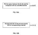
- flowchart 600includes the step shown in FIG. 10A .
- step 1005a space between the active surface of the IC die and the interposer is filled in with an underfill material.
- the IC dieis IC die 205
- the active surface of the IC dieis active surface 202
- the interposeris interposer 240
- the underfill materialis underfill material 265 , as shown in FIG. 2D .
- flowchart 600includes the step shown in FIG. 10B .
- the IC die and the wire bondsare encapsulated with an encapsulating material.
- the IC dieis IC die 205
- the wire bondsare wire bonds 230
- the encapsulating materialis encapsulating material 260 , as shown in FIGS. 2A , 2 D, and 3 - 5 .
Landscapes
- Engineering & Computer Science (AREA)
- Microelectronics & Electronic Packaging (AREA)
- Physics & Mathematics (AREA)
- Condensed Matter Physics & Semiconductors (AREA)
- General Physics & Mathematics (AREA)
- Computer Hardware Design (AREA)
- Power Engineering (AREA)
- Chemical & Material Sciences (AREA)
- Materials Engineering (AREA)
- Cooling Or The Like Of Semiconductors Or Solid State Devices (AREA)
Abstract
Description
Claims (21)
Priority Applications (2)
| Application Number | Priority Date | Filing Date | Title |
|---|---|---|---|
| US10/870,928US7411281B2 (en) | 2004-06-21 | 2004-06-21 | Integrated circuit device package having both wire bond and flip-chip interconnections and method of making the same |
| US12/058,067US7595227B2 (en) | 2004-06-21 | 2008-03-28 | Integrated circuit device package having both wire bond and flip-chip interconnections and method of making the same |
Applications Claiming Priority (1)
| Application Number | Priority Date | Filing Date | Title |
|---|---|---|---|
| US10/870,928US7411281B2 (en) | 2004-06-21 | 2004-06-21 | Integrated circuit device package having both wire bond and flip-chip interconnections and method of making the same |
Related Child Applications (1)
| Application Number | Title | Priority Date | Filing Date |
|---|---|---|---|
| US12/058,067DivisionUS7595227B2 (en) | 2004-06-21 | 2008-03-28 | Integrated circuit device package having both wire bond and flip-chip interconnections and method of making the same |
Publications (2)
| Publication Number | Publication Date |
|---|---|
| US20050280141A1 US20050280141A1 (en) | 2005-12-22 |
| US7411281B2true US7411281B2 (en) | 2008-08-12 |
Family
ID=35479792
Family Applications (2)
| Application Number | Title | Priority Date | Filing Date |
|---|---|---|---|
| US10/870,928Expired - Fee RelatedUS7411281B2 (en) | 2004-06-21 | 2004-06-21 | Integrated circuit device package having both wire bond and flip-chip interconnections and method of making the same |
| US12/058,067Expired - Fee RelatedUS7595227B2 (en) | 2004-06-21 | 2008-03-28 | Integrated circuit device package having both wire bond and flip-chip interconnections and method of making the same |
Family Applications After (1)
| Application Number | Title | Priority Date | Filing Date |
|---|---|---|---|
| US12/058,067Expired - Fee RelatedUS7595227B2 (en) | 2004-06-21 | 2008-03-28 | Integrated circuit device package having both wire bond and flip-chip interconnections and method of making the same |
Country Status (1)
| Country | Link |
|---|---|
| US (2) | US7411281B2 (en) |
Cited By (21)
| Publication number | Priority date | Publication date | Assignee | Title |
|---|---|---|---|---|
| US20070029663A1 (en)* | 2005-08-08 | 2007-02-08 | Moon-Jung Kim | Multilayered circuit substrate and semiconductor package structure using the same |
| US20070040267A1 (en)* | 2005-08-22 | 2007-02-22 | Broadcom Corporation | Method and system for secure heat sink attachment on semiconductor devices with macroscopic uneven surface features |
| US20070273049A1 (en)* | 2006-05-12 | 2007-11-29 | Broadcom Corporation | Interconnect structure and formation for package stacking of molded plastic area array package |
| US20070273023A1 (en)* | 2006-05-26 | 2007-11-29 | Broadcom Corporation | Integrated circuit package having exposed thermally conducting body |
| US20080096312A1 (en)* | 2006-10-20 | 2008-04-24 | Broadcom Corporation | Low profile ball grid array (BGA) package with exposed die and method of making same |
| RU2386190C1 (en)* | 2008-12-05 | 2010-04-10 | Закрытое акционерное общество "Научно-производственное объединение "НИИТАЛ" (ЗАО "НПО "НИИТАЛ") | Body of integrated circuit |
| US7781266B2 (en) | 2005-10-20 | 2010-08-24 | Broadcom Corporation | Methods and apparatus for improved thermal performance and electromagnetic interference (EMI) shielding in leadframe integrated circuit (IC) packages |
| US7786591B2 (en)* | 2004-09-29 | 2010-08-31 | Broadcom Corporation | Die down ball grid array package |
| US20110159640A1 (en)* | 2006-09-26 | 2011-06-30 | Compass Technology Co., Inc. | Multiple integrated circuit die package with thermal performance |
| US20120056178A1 (en)* | 2010-09-06 | 2012-03-08 | Samsung Electronics Co., Ltd. | Multi-chip packages |
| US20130078915A1 (en)* | 2011-09-28 | 2013-03-28 | Broadcom Corporation | Interposer Package Structure for Wireless Communication Element, Thermal Enhancement, and EMI Shielding |
| US8581381B2 (en) | 2006-06-20 | 2013-11-12 | Broadcom Corporation | Integrated circuit (IC) package stacking and IC packages formed by same |
| US9209121B2 (en) | 2013-02-01 | 2015-12-08 | Analog Devices, Inc. | Double-sided package |
| US9533878B2 (en) | 2014-12-11 | 2017-01-03 | Analog Devices, Inc. | Low stress compact device packages |
| US9638596B2 (en) | 2014-04-08 | 2017-05-02 | Freescale Semiconductor, Inc. | Cavity-down pressure sensor device |
| US9731959B2 (en) | 2014-09-25 | 2017-08-15 | Analog Devices, Inc. | Integrated device packages having a MEMS die sealed in a cavity by a processor die and method of manufacturing the same |
| US11209598B2 (en) | 2019-02-28 | 2021-12-28 | International Business Machines Corporation | Photonics package with face-to-face bonding |
| US11296005B2 (en) | 2019-09-24 | 2022-04-05 | Analog Devices, Inc. | Integrated device package including thermally conductive element and method of manufacturing same |
| US20220283387A1 (en)* | 2021-03-03 | 2022-09-08 | Taiwan Semiconductor Manufacturing Co., Ltd. | Heterogeneous packaging integration of photonic and electronic elements |
| US11516912B2 (en) | 2019-12-18 | 2022-11-29 | Samsung Electronics Co., Ltd | Printed circuit board and electronic device having the same |
| US12315776B2 (en) | 2021-11-08 | 2025-05-27 | Analog Devices, Inc. | Integrated device package with an integrated heat sink |
Families Citing this family (30)
| Publication number | Priority date | Publication date | Assignee | Title |
|---|---|---|---|---|
| CN100370580C (en)* | 2004-03-29 | 2008-02-20 | 雅马哈株式会社 | Semiconductor wafer and method for manufacturing the same |
| TWI234860B (en)* | 2004-04-02 | 2005-06-21 | Advanced Semiconductor Eng | Chip package and process thereof |
| US7271479B2 (en)* | 2004-11-03 | 2007-09-18 | Broadcom Corporation | Flip chip package including a non-planar heat spreader and method of making the same |
| KR100618892B1 (en)* | 2005-04-13 | 2006-09-01 | 삼성전자주식회사 | Semiconductor package achieves fan-out structure through wire bonding |
| KR100885419B1 (en)* | 2006-04-26 | 2009-02-24 | 삼성전자주식회사 | Stacked Package Structure |
| US9299634B2 (en)* | 2006-05-16 | 2016-03-29 | Broadcom Corporation | Method and apparatus for cooling semiconductor device hot blocks and large scale integrated circuit (IC) using integrated interposer for IC packages |
| US8183680B2 (en) | 2006-05-16 | 2012-05-22 | Broadcom Corporation | No-lead IC packages having integrated heat spreader for electromagnetic interference (EMI) shielding and thermal enhancement |
| US7808087B2 (en)* | 2006-06-01 | 2010-10-05 | Broadcom Corporation | Leadframe IC packages having top and bottom integrated heat spreaders |
| US9013035B2 (en)* | 2006-06-20 | 2015-04-21 | Broadcom Corporation | Thermal improvement for hotspots on dies in integrated circuit packages |
| US8183687B2 (en) | 2007-02-16 | 2012-05-22 | Broadcom Corporation | Interposer for die stacking in semiconductor packages and the method of making the same |
| US20080298024A1 (en)* | 2007-05-31 | 2008-12-04 | A.L.M.T. Corp. | Heat spreader and method for manufacturing the same, and semiconductor device |
| US7872335B2 (en)* | 2007-06-08 | 2011-01-18 | Broadcom Corporation | Lead frame-BGA package with enhanced thermal performance and I/O counts |
| US20090283889A1 (en)* | 2008-05-16 | 2009-11-19 | Byoung Wook Jang | Integrated circuit package system |
| US8633597B2 (en)* | 2010-03-01 | 2014-01-21 | Qualcomm Incorporated | Thermal vias in an integrated circuit package with an embedded die |
| US8780600B2 (en)* | 2011-12-07 | 2014-07-15 | Apple Inc. | Systems and methods for stacked semiconductor memory devices |
| CN105210185A (en)* | 2013-05-17 | 2015-12-30 | 富士通株式会社 | Semiconductor device, semiconductor device manufacturing method, and electronic apparatus |
| US9318411B2 (en)* | 2013-11-13 | 2016-04-19 | Brodge Semiconductor Corporation | Semiconductor package with package-on-package stacking capability and method of manufacturing the same |
| EP2947692B1 (en)* | 2013-12-20 | 2020-09-23 | Analog Devices, Inc. | Integrated device die and package with stress reduction features |
| KR102228461B1 (en)* | 2014-04-30 | 2021-03-17 | 삼성전자주식회사 | Semiconductor Package Device |
| US20150340308A1 (en)* | 2014-05-21 | 2015-11-26 | Broadcom Corporation | Reconstituted interposer semiconductor package |
| US9401612B2 (en) | 2014-09-16 | 2016-07-26 | Navitas Semiconductor Inc. | Pulsed level shift and inverter circuits for GaN devices |
| KR20170001238A (en)* | 2015-06-26 | 2017-01-04 | 에스케이하이닉스 주식회사 | Semiconductor package including step type substrate |
| US10287161B2 (en) | 2015-07-23 | 2019-05-14 | Analog Devices, Inc. | Stress isolation features for stacked dies |
| US9570372B1 (en)* | 2016-03-24 | 2017-02-14 | Bridge Semiconductor Corporation | Thermally enhanced semiconductor assembly with heat spreader and integrated dual build-up circuitries and method of making the same |
| US11112841B2 (en)* | 2017-04-01 | 2021-09-07 | Intel Corporation | 5G mmWave cooling through PCB |
| CN107369663A (en)* | 2017-08-25 | 2017-11-21 | 广东工业大学 | A kind of chip of fan-out package structure for possessing front salient point and preparation method thereof |
| US11127716B2 (en) | 2018-04-12 | 2021-09-21 | Analog Devices International Unlimited Company | Mounting structures for integrated device packages |
| JP7290201B2 (en) | 2020-06-05 | 2023-06-13 | 日本電気株式会社 | quantum device |
| US11664340B2 (en) | 2020-07-13 | 2023-05-30 | Analog Devices, Inc. | Negative fillet for mounting an integrated device die to a carrier |
| US20230090133A1 (en)* | 2021-09-21 | 2023-03-23 | Bai Nie | Die first fan-out architecture for electric and optical integration |
Citations (160)
| Publication number | Priority date | Publication date | Assignee | Title |
|---|---|---|---|---|
| US3790866A (en) | 1973-05-14 | 1974-02-05 | Gen Motors Corp | Semiconductor device enclosure and method of making same |
| JPS6149446A (en) | 1984-08-17 | 1986-03-11 | Matsushita Electronics Corp | Resin seal type semiconductor device |
| US4611238A (en) | 1982-05-05 | 1986-09-09 | Burroughs Corporation | Integrated circuit package incorporating low-stress omnidirectional heat sink |
| US5045921A (en) | 1989-12-26 | 1991-09-03 | Motorola, Inc. | Pad array carrier IC device using flexible tape |
| US5065281A (en) | 1990-02-12 | 1991-11-12 | Rogers Corporation | Molded integrated circuit package incorporating heat sink |
| US5173766A (en) | 1990-06-25 | 1992-12-22 | Lsi Logic Corporation | Semiconductor device package and method of making such a package |
| US5208504A (en) | 1990-12-28 | 1993-05-04 | Raytheon Company | Saw device and method of manufacture |
| US5216278A (en) | 1990-12-04 | 1993-06-01 | Motorola, Inc. | Semiconductor device having a pad array carrier package |
| EP0573297A2 (en) | 1992-06-04 | 1993-12-08 | Shinko Electric Industries Co. Ltd. | Semiconductor device comprising a TAB tape |
| US5285352A (en) | 1992-07-15 | 1994-02-08 | Motorola, Inc. | Pad array semiconductor device with thermal conductor and process for making the same |
| US5291062A (en) | 1993-03-01 | 1994-03-01 | Motorola, Inc. | Area array semiconductor device having a lid with functional contacts |
| US5294826A (en) | 1993-04-16 | 1994-03-15 | Northern Telecom Limited | Integrated circuit package and assembly thereof for thermal and EMI management |
| US5366589A (en) | 1993-11-16 | 1994-11-22 | Motorola, Inc. | Bonding pad with circular exposed area and method thereof |
| US5394009A (en) | 1993-07-30 | 1995-02-28 | Sun Microsystems, Inc. | Tab semiconductor package with cushioned land grid array outer lead bumps |
| US5397921A (en) | 1993-09-03 | 1995-03-14 | Advanced Semiconductor Assembly Technology | Tab grid array |
| US5397917A (en) | 1993-04-26 | 1995-03-14 | Motorola, Inc. | Semiconductor package capable of spreading heat |
| US5433631A (en) | 1993-01-26 | 1995-07-18 | International Business Machines Corporation | Flex circuit card elastomeric cable connector assembly |
| US5438216A (en) | 1992-08-31 | 1995-08-01 | Motorola, Inc. | Light erasable multichip module |
| JPH07283336A (en) | 1994-04-05 | 1995-10-27 | Toppan Printing Co Ltd | Chip carrier |
| US5474957A (en) | 1994-05-09 | 1995-12-12 | Nec Corporation | Process of mounting tape automated bonded semiconductor chip on printed circuit board through bumps |
| US5490324A (en) | 1993-09-15 | 1996-02-13 | Lsi Logic Corporation | Method of making integrated circuit package having multiple bonding tiers |
| US5534467A (en) | 1993-03-18 | 1996-07-09 | Lsi Logic Corporation | Semiconductor packages for high I/O semiconductor dies |
| US5541450A (en) | 1994-11-02 | 1996-07-30 | Motorola, Inc. | Low-profile ball-grid array semiconductor package |
| US5552635A (en) | 1994-01-11 | 1996-09-03 | Samsung Electronics Co., Ltd. | High thermal emissive semiconductor device package |
| US5572405A (en) | 1995-06-07 | 1996-11-05 | International Business Machines Corporation (Ibm) | Thermally enhanced ball grid array package |
| US5578869A (en) | 1994-03-29 | 1996-11-26 | Olin Corporation | Components for housing an integrated circuit device |
| US5583378A (en) | 1994-05-16 | 1996-12-10 | Amkor Electronics, Inc. | Ball grid array integrated circuit package with thermal conductor |
| US5583377A (en) | 1992-07-15 | 1996-12-10 | Motorola, Inc. | Pad array semiconductor device having a heat sink with die receiving cavity |
| US5642261A (en) | 1993-12-20 | 1997-06-24 | Sgs-Thomson Microelectronics, Inc. | Ball-grid-array integrated circuit package with solder-connected thermal conductor |
| US5648679A (en) | 1994-09-16 | 1997-07-15 | National Semiconductor Corporation | Tape ball lead integrated circuit package |
| US5650659A (en) | 1995-08-04 | 1997-07-22 | National Semiconductor Corporation | Semiconductor component package assembly including an integral RF/EMI shield |
| US5650662A (en) | 1993-08-17 | 1997-07-22 | Edwards; Steven F. | Direct bonded heat spreader |
| US5691567A (en) | 1995-09-19 | 1997-11-25 | National Semiconductor Corporation | Structure for attaching a lead frame to a heat spreader/heat slug structure |
| US5717252A (en) | 1994-07-25 | 1998-02-10 | Mitsui High-Tec, Inc. | Solder-ball connected semiconductor device with a recessed chip mounting area |
| JPH1050877A (en) | 1996-07-30 | 1998-02-20 | Toshiba Corp | Semiconductor package |
| US5736785A (en) | 1996-12-20 | 1998-04-07 | Industrial Technology Research Institute | Semiconductor package for improving the capability of spreading heat |
| US5744863A (en) | 1994-07-11 | 1998-04-28 | International Business Machines Corporation | Chip carrier modules with heat sinks attached by flexible-epoxy |
| EP0504411B1 (en) | 1990-09-19 | 1998-06-17 | Fujitsu Limited | Semiconductor device having many lead pins |
| JPH10189835A (en) | 1996-12-16 | 1998-07-21 | Lg Electron Inc | Semiconductor package and its assembling method |
| US5796170A (en) | 1996-02-15 | 1998-08-18 | Northern Telecom Limited | Ball grid array (BGA) integrated circuit packages |
| US5798909A (en) | 1995-02-15 | 1998-08-25 | International Business Machines Corporation | Single-tiered organic chip carriers for wire bond-type chips |
| US5801432A (en) | 1992-06-04 | 1998-09-01 | Lsi Logic Corporation | Electronic system using multi-layer tab tape semiconductor device having distinct signal, power and ground planes |
| JPH10247703A (en) | 1997-03-05 | 1998-09-14 | Sumitomo Kinzoku Electro Device:Kk | Ball grid array package and printed board |
| JPH10247702A (en) | 1997-03-05 | 1998-09-14 | Sumitomo Kinzoku Electro Device:Kk | Ball grid array package and printed board |
| US5835355A (en) | 1997-09-22 | 1998-11-10 | Lsi Logic Corporation | Tape ball grid array package with perforated metal stiffener |
| US5844168A (en) | 1995-08-01 | 1998-12-01 | Minnesota Mining And Manufacturing Company | Multi-layer interconnect sutructure for ball grid arrays |
| US5843808A (en) | 1996-01-11 | 1998-12-01 | Asat, Limited | Structure and method for automated assembly of a tab grid array package |
| US5856911A (en) | 1996-11-12 | 1999-01-05 | National Semiconductor Corporation | Attachment assembly for integrated circuits |
| JPH1117064A (en) | 1997-06-24 | 1999-01-22 | Toshiba Corp | Semiconductor package |
| US5866949A (en) | 1996-12-02 | 1999-02-02 | Minnesota Mining And Manufacturing Company | Chip scale ball grid array for integrated circuit packaging |
| US5883430A (en) | 1996-06-19 | 1999-03-16 | International Business Machines Corporation | Thermally enhanced flip chip package |
| US5889324A (en) | 1998-03-30 | 1999-03-30 | Nec Corporation | Package for a semiconductor device |
| US5889321A (en) | 1997-06-17 | 1999-03-30 | International Business Machines Corporation | Stiffeners with improved adhesion to flexible substrates |
| JPH11102989A (en) | 1997-09-26 | 1999-04-13 | Hitachi Cable Ltd | BGA type semiconductor device |
| US5894410A (en) | 1996-03-28 | 1999-04-13 | Intel Corporation | Perimeter matrix ball grid array circuit package with a populated center |
| US5895967A (en) | 1997-07-07 | 1999-04-20 | Texas Instruments Incorporated | Ball grid array package having a deformable metal layer and method |
| US5901041A (en) | 1997-12-02 | 1999-05-04 | Northern Telecom Limited | Flexible integrated circuit package |
| US5903052A (en) | 1998-05-12 | 1999-05-11 | Industrial Technology Research Institute | Structure for semiconductor package for improving the efficiency of spreading heat |
| US5905633A (en) | 1996-02-29 | 1999-05-18 | Anam Semiconductor Inc. | Ball grid array semiconductor package using a metal carrier ring as a heat spreader |
| US5907189A (en) | 1997-05-29 | 1999-05-25 | Lsi Logic Corporation | Conformal diamond coating for thermal improvement of electronic packages |
| US5907903A (en) | 1996-05-24 | 1999-06-01 | International Business Machines Corporation | Multi-layer-multi-chip pyramid and circuit board structure and method of forming same |
| US5920117A (en) | 1994-08-02 | 1999-07-06 | Fujitsu Limited | Semiconductor device and method of forming the device |
| US5949137A (en) | 1997-09-26 | 1999-09-07 | Lsi Logic Corporation | Stiffener ring and heat spreader for use with flip chip packaging assemblies |
| US5953589A (en) | 1996-12-30 | 1999-09-14 | Anam Semiconductor Inc. | Ball grid array semiconductor package with solder balls fused on printed circuit board and method for fabricating the same |
| US5972734A (en) | 1997-09-17 | 1999-10-26 | Lsi Logic Corporation | Interposer for ball grid array (BGA) package |
| US5977633A (en) | 1996-08-15 | 1999-11-02 | Nec Corporation | Semiconductor device with metal base substrate having hollows |
| US5977626A (en) | 1998-08-12 | 1999-11-02 | Industrial Technology Research Institute | Thermally and electrically enhanced PBGA package |
| US5976912A (en) | 1994-03-18 | 1999-11-02 | Hitachi Chemical Company, Ltd. | Fabrication process of semiconductor package and semiconductor package |
| US5982621A (en) | 1998-11-23 | 1999-11-09 | Caesar Technology Inc. | Electronic device cooling arrangement |
| US5986340A (en) | 1996-05-02 | 1999-11-16 | National Semiconductor Corporation | Ball grid array package with enhanced thermal and electrical characteristics and electronic device incorporating same |
| US5986885A (en) | 1997-04-08 | 1999-11-16 | Integrated Device Technology, Inc. | Semiconductor package with internal heatsink and assembly method |
| US5999415A (en) | 1998-11-18 | 1999-12-07 | Vlsi Technology, Inc. | BGA package using PCB and tape in a die-down configuration |
| US5998241A (en) | 1997-12-08 | 1999-12-07 | Nec Corporation | Semiconductor device and method of manufacturing the same |
| US6002147A (en) | 1996-09-26 | 1999-12-14 | Samsung Electronics Company | Hybrid microwave-frequency integrated circuit |
| US6002169A (en) | 1998-06-15 | 1999-12-14 | Lsi Logic Corporation | Thermally enhanced tape ball grid array package |
| US6011304A (en) | 1997-05-05 | 2000-01-04 | Lsi Logic Corporation | Stiffener ring attachment with holes and removable snap-in heat sink or heat spreader/lid |
| US6011694A (en) | 1996-08-01 | 2000-01-04 | Fuji Machinery Mfg. & Electronics Co., Ltd. | Ball grid array semiconductor package with solder ball openings in an insulative base |
| US6020637A (en) | 1997-05-07 | 2000-02-01 | Signetics Kp Co., Ltd. | Ball grid array semiconductor package |
| US6028358A (en) | 1996-05-30 | 2000-02-22 | Nec Corporation | Package for a semiconductor device and a semiconductor device |
| TW383908U (en) | 1998-09-22 | 2000-03-01 | Caesar Technology Inc | Structure used for increasing heat-dissipation of micro-electronic apparatus |
| US6034427A (en) | 1998-01-28 | 2000-03-07 | Prolinx Labs Corporation | Ball grid array structure and method for packaging an integrated circuit chip |
| US6040984A (en) | 1996-02-27 | 2000-03-21 | Fuji Machinery Mfg. & Electronics Co., Ltd. | Printed circuit board with opposed bonding shelves for semiconductor chip wire bonding at different levels |
| US6057601A (en) | 1998-11-27 | 2000-05-02 | Express Packaging Systems, Inc. | Heat spreader with a placement recess and bottom saw-teeth for connection to ground planes on a thin two-sided single-core BGA substrate |
| US6060777A (en) | 1998-07-21 | 2000-05-09 | Intel Corporation | Underside heat slug for ball grid array packages |
| US6064111A (en) | 1996-07-31 | 2000-05-16 | Hitachi Company, Ltd. | Substrate for holding a chip of semi-conductor package, semi-conductor package, and fabrication process of semi-conductor package |
| US6069407A (en) | 1998-11-18 | 2000-05-30 | Vlsi Technology, Inc. | BGA package using PCB and tape in a die-up configuration |
| US6077724A (en) | 1998-09-05 | 2000-06-20 | First International Computer Inc. | Multi-chips semiconductor package and fabrication method |
| US6084297A (en) | 1998-09-03 | 2000-07-04 | Micron Technology, Inc. | Cavity ball grid array apparatus |
| US6084777A (en) | 1997-04-23 | 2000-07-04 | Texas Instruments Incorporated | Ball grid array package |
| US6114761A (en) | 1998-01-20 | 2000-09-05 | Lsi Logic Corporation | Thermally-enhanced flip chip IC package with extruded heatspreader |
| US6117797A (en) | 1998-09-03 | 2000-09-12 | Micron Technology, Inc. | Attachment method for heat sinks and devices involving removal of misplaced encapsulant |
| US6122171A (en) | 1999-07-30 | 2000-09-19 | Micron Technology, Inc. | Heat sink chip package and method of making |
| JP2000286294A (en) | 1999-03-30 | 2000-10-13 | Hitachi Ltd | Semiconductor device and manufacturing method thereof |
| US6133064A (en) | 1999-05-27 | 2000-10-17 | Lsi Logic Corporation | Flip chip ball grid array package with laminated substrate |
| US6140707A (en) | 1998-05-07 | 2000-10-31 | 3M Innovative Properties Co. | Laminated integrated circuit package |
| US6160705A (en) | 1997-05-09 | 2000-12-12 | Texas Instruments Incorporated | Ball grid array package and method using enhanced power and ground distribution circuitry |
| US6163458A (en) | 1999-12-03 | 2000-12-19 | Caesar Technology, Inc. | Heat spreader for ball grid array package |
| US6162659A (en) | 1999-03-05 | 2000-12-19 | International Business Machines Corporation | Method for manufacturing a package structure having a heat spreader for integrated circuit chips |
| US6166434A (en) | 1997-09-23 | 2000-12-26 | Lsi Logic Corporation | Die clip assembly for semiconductor package |
| TW417219B (en) | 1999-07-22 | 2001-01-01 | Siliconware Precision Industries Co Ltd | Ball grid array package having leads |
| US6184580B1 (en) | 1999-09-10 | 2001-02-06 | Siliconware Precision Industries Co., Ltd. | Ball grid array package with conductive leads |
| US6201300B1 (en) | 1998-04-22 | 2001-03-13 | World Wiser Electronics Inc. | Printed circuit board with thermal conductive structure |
| JP2001068512A (en) | 1999-08-27 | 2001-03-16 | Hitachi Cable Ltd | TAB tape and BGA package with stiffener |
| US6207467B1 (en) | 1999-08-17 | 2001-03-27 | Micron Technology, Inc. | Multi-chip module with stacked dice |
| US6212070B1 (en) | 1996-07-22 | 2001-04-03 | International Business Machines Corporation | Zero force heat sink |
| US20010001505A1 (en) | 1998-10-14 | 2001-05-24 | 3M Innovative Properties Company | Tape ball grid array with interconnected ground plane |
| US6242279B1 (en) | 1999-06-14 | 2001-06-05 | Thin Film Module, Inc. | High density wire bond BGA |
| US6246111B1 (en) | 2000-01-25 | 2001-06-12 | Siliconware Precision Industries Co., Ltd. | Universal lead frame type of quad flat non-lead package of semiconductor |
| FR2803098A3 (en) | 1999-12-22 | 2001-06-29 | Orient Semiconductor Elect Ltd | Heat sink for plastic ball grid array on IC chip surface has antioxidant coating on protruding body mounted on chip surface to form an elastic connecting structure using material adhesion |
| US6278613B1 (en) | 2000-09-27 | 2001-08-21 | St Assembly Test Services Pte Ltd | Copper pads for heat spreader attach |
| US6288444B1 (en) | 1998-11-17 | 2001-09-11 | Fujitsu Limited | Semiconductor device and method of producing the same |
| US6313525B1 (en) | 1997-07-10 | 2001-11-06 | Sony Corporation | Hollow package and method for fabricating the same and solid-state image apparatus provided therewith |
| US6313521B1 (en) | 1998-11-04 | 2001-11-06 | Nec Corporation | Semiconductor device and method of manufacturing the same |
| US20010040279A1 (en) | 1999-08-30 | 2001-11-15 | Mess Leonard E. | Apparatus and methods of packaging and testing die |
| US20010045644A1 (en) | 2000-01-13 | 2001-11-29 | Chien-Ping Huang | Semiconductor package having heat sink at the outer surface |
| US6347037B2 (en) | 1994-04-28 | 2002-02-12 | Fujitsu Limited | Semiconductor device and method of forming the same |
| US6362525B1 (en) | 1999-11-09 | 2002-03-26 | Cypress Semiconductor Corp. | Circuit structure including a passive element formed within a grid array substrate and method for making the same |
| US6365980B1 (en) | 1999-02-26 | 2002-04-02 | Texas Instruments Incorporated | Thermally enhanced semiconductor ball grid array device and method of fabrication |
| US6369455B1 (en) | 2000-01-04 | 2002-04-09 | Siliconware Precision Industries Co., Ltd. | Externally-embedded heat-dissipating device for ball grid array integrated circuit package |
| US6380623B1 (en) | 1999-10-15 | 2002-04-30 | Hughes Electronics Corporation | Microcircuit assembly having dual-path grounding and negative self-bias |
| US20020053731A1 (en) | 2000-11-08 | 2002-05-09 | Shin-Hua Chao | Structure and package of a heat spreader substrate |
| US6395582B1 (en)* | 1997-07-14 | 2002-05-28 | Signetics | Methods for forming ground vias in semiconductor packages |
| US20020072214A1 (en) | 1998-10-28 | 2002-06-13 | Seiko Epson Corporation | Semiconductor device and method of fabrication thereof, circuit board, and electronic equipment |
| US20020079572A1 (en) | 2000-12-22 | 2002-06-27 | Khan Reza-Ur Rahman | Enhanced die-up ball grid array and method for making the same |
| US20020079562A1 (en) | 2000-12-22 | 2002-06-27 | Broadcom Corporation | Enhanced die-up ball grid array packages and method for making the same |
| US20020096767A1 (en) | 2001-01-25 | 2002-07-25 | Cote Kevin J. | Cavity down ball grid array package with EMI shielding and reduced thermal resistance |
| US20020098617A1 (en) | 2001-01-20 | 2002-07-25 | Ming-Xun Lee | CD BGA package and a fabrication method thereof |
| US20020109226A1 (en) | 2001-02-15 | 2002-08-15 | Broadcom Corporation | Enhanced die-down ball grid array and method for making the same |
| US20020135065A1 (en) | 2000-12-01 | 2002-09-26 | Zhao Sam Ziqun | Thermally and electrically enhanced ball grid array packaging |
| US6462274B1 (en) | 1998-10-31 | 2002-10-08 | Amkor Technology, Inc. | Chip-scale semiconductor package of the fan-out type and method of manufacturing such packages |
| US6472741B1 (en) | 2001-07-14 | 2002-10-29 | Siliconware Precision Industries Co., Ltd. | Thermally-enhanced stacked-die ball grid array semiconductor package and method of fabricating the same |
| US20020171144A1 (en) | 2001-05-07 | 2002-11-21 | Broadcom Corporation | Die-up ball grid array package with a heat spreader and method for making the same |
| US20020180040A1 (en) | 2001-05-30 | 2002-12-05 | St Assembly Test Services Pte Ltd | Super thin/super thermal ball grid array package |
| US20020185717A1 (en) | 2001-06-11 | 2002-12-12 | Xilinx, Inc. | High performance flipchip package that incorporates heat removal with minimal thermal mismatch |
| US6525942B2 (en) | 2000-09-19 | 2003-02-25 | Siliconware Precision Industries Co., Ltd. | Heat dissipation ball grid array package |
| US6528869B1 (en) | 2001-04-06 | 2003-03-04 | Amkor Technology, Inc. | Semiconductor package with molded substrate and recessed input/output terminals |
| US6528892B2 (en) | 2001-06-05 | 2003-03-04 | International Business Machines Corporation | Land grid array stiffener use with flexible chip carriers |
| US20030057550A1 (en) | 2000-12-22 | 2003-03-27 | Broadcom Corporation | Ball grid array package enhanced with a thermal and electrical connector |
| US6541832B2 (en) | 2000-01-31 | 2003-04-01 | Texas Instruments Incorporated | Plastic package for micromechanical devices |
| US6552428B1 (en) | 1998-10-12 | 2003-04-22 | Siliconware Precision Industries Co., Ltd. | Semiconductor package having an exposed heat spreader |
| US6552430B1 (en) | 2002-01-30 | 2003-04-22 | Texas Instruments Incorporated | Ball grid array substrate with improved traces formed from copper based metal |
| US6552266B2 (en) | 1998-03-11 | 2003-04-22 | International Business Machines Corporation | High performance chip packaging and method |
| US20030111726A1 (en) | 2001-12-18 | 2003-06-19 | Khan Reza-Ur Rahman | Ball grid array package substrates and method of making the same |
| US6583516B2 (en) | 1998-03-23 | 2003-06-24 | Seiko Epson Corporation | Semiconductor device and method of manufacturing the same, circuit board, and electronic instrument |
| US20030137057A1 (en)* | 2002-01-24 | 2003-07-24 | Nec Electronics Corporation | Flip chip type semiconductor device and method of manufacturing the same |
| US20030138613A1 (en) | 2002-01-24 | 2003-07-24 | Steve Thoman | Lightweight thermal heat transfer apparatus |
| US6602732B2 (en) | 2000-01-14 | 2003-08-05 | Computech International Ventures Limited | Method for mounting a semiconductor chip on a substrate and semiconductor device adapted for mounting on a substrate |
| US20030146503A1 (en) | 2002-02-01 | 2003-08-07 | Broadcom Corporation | Ball grid array package with stepped stiffener layer |
| US20030146509A1 (en) | 2002-02-01 | 2003-08-07 | Broadcom Corporation | Ball grid array package with separated stiffener layer |
| US20030146506A1 (en) | 2002-02-01 | 2003-08-07 | Broadcom Corporation | Ball grid array package fabrication with IC die support structures |
| US20030146511A1 (en) | 2002-02-01 | 2003-08-07 | Broadcom Corporation | Ball grid array package with multiple interposers |
| US6614660B1 (en) | 2002-04-30 | 2003-09-02 | Ultratera Corporation | Thermally enhanced IC chip package |
| US6617193B1 (en) | 1997-04-30 | 2003-09-09 | Hitachi Chemical Company, Ltd. | Semiconductor device, semiconductor device substrate, and methods of fabricating the same |
| US20030179549A1 (en) | 2002-03-22 | 2003-09-25 | Zhong Chong Hua | Low voltage drop and high thermal perfor mance ball grid array package |
| US20030179556A1 (en) | 2002-03-21 | 2003-09-25 | Broadcom Corporation | Enhanced die-up ball grid array package with two substrates and method for making the same |
| US6657870B1 (en) | 2001-10-01 | 2003-12-02 | Lsi Logic Corporation | Die power distribution system |
| US6664617B2 (en) | 2000-12-19 | 2003-12-16 | Convergence Technologies, Ltd. | Semiconductor package |
| US20040072456A1 (en) | 1993-11-16 | 2004-04-15 | Formfactor, Inc. | Methods of removably mounting electronic components to a circuit board, and sockets formed by the methods |
| US6724071B2 (en) | 1993-09-03 | 2004-04-20 | Asat, Limited | Molded plastic package with heat sink and enhanced electrical performance |
| US6724080B1 (en) | 2002-12-20 | 2004-04-20 | Altera Corporation | Heat sink with elevated heat spreader lid |
Family Cites Families (5)
| Publication number | Priority date | Publication date | Assignee | Title |
|---|---|---|---|---|
| US599415A (en)* | 1898-02-22 | Cromwell | ||
| JPH06324051A (en)* | 1993-05-11 | 1994-11-25 | Olympus Optical Co Ltd | Plug opener |
| US6084397A (en)* | 1997-12-22 | 2000-07-04 | Emc Corporation | Verification gauge for an electronic package lead inspection apparatus |
| US6011340A (en)* | 1998-04-22 | 2000-01-04 | Axis Usa, Inc. | Dynamo-electric apparatus and methods for manufacturing |
| SG108245A1 (en)* | 2001-03-30 | 2005-01-28 | Micron Technology Inc | Ball grid array interposer, packages and methods |
- 2004
- 2004-06-21USUS10/870,928patent/US7411281B2/ennot_activeExpired - Fee Related
- 2008
- 2008-03-28USUS12/058,067patent/US7595227B2/ennot_activeExpired - Fee Related
Patent Citations (170)
| Publication number | Priority date | Publication date | Assignee | Title |
|---|---|---|---|---|
| US3790866A (en) | 1973-05-14 | 1974-02-05 | Gen Motors Corp | Semiconductor device enclosure and method of making same |
| US4611238A (en) | 1982-05-05 | 1986-09-09 | Burroughs Corporation | Integrated circuit package incorporating low-stress omnidirectional heat sink |
| JPS6149446A (en) | 1984-08-17 | 1986-03-11 | Matsushita Electronics Corp | Resin seal type semiconductor device |
| US5045921A (en) | 1989-12-26 | 1991-09-03 | Motorola, Inc. | Pad array carrier IC device using flexible tape |
| US5065281A (en) | 1990-02-12 | 1991-11-12 | Rogers Corporation | Molded integrated circuit package incorporating heat sink |
| US5173766A (en) | 1990-06-25 | 1992-12-22 | Lsi Logic Corporation | Semiconductor device package and method of making such a package |
| EP0504411B1 (en) | 1990-09-19 | 1998-06-17 | Fujitsu Limited | Semiconductor device having many lead pins |
| US5216278A (en) | 1990-12-04 | 1993-06-01 | Motorola, Inc. | Semiconductor device having a pad array carrier package |
| US5208504A (en) | 1990-12-28 | 1993-05-04 | Raytheon Company | Saw device and method of manufacture |
| US5801432A (en) | 1992-06-04 | 1998-09-01 | Lsi Logic Corporation | Electronic system using multi-layer tab tape semiconductor device having distinct signal, power and ground planes |
| EP0573297A2 (en) | 1992-06-04 | 1993-12-08 | Shinko Electric Industries Co. Ltd. | Semiconductor device comprising a TAB tape |
| US5285352A (en) | 1992-07-15 | 1994-02-08 | Motorola, Inc. | Pad array semiconductor device with thermal conductor and process for making the same |
| US5583377A (en) | 1992-07-15 | 1996-12-10 | Motorola, Inc. | Pad array semiconductor device having a heat sink with die receiving cavity |
| US5438216A (en) | 1992-08-31 | 1995-08-01 | Motorola, Inc. | Light erasable multichip module |
| US5433631A (en) | 1993-01-26 | 1995-07-18 | International Business Machines Corporation | Flex circuit card elastomeric cable connector assembly |
| US5291062A (en) | 1993-03-01 | 1994-03-01 | Motorola, Inc. | Area array semiconductor device having a lid with functional contacts |
| US5534467A (en) | 1993-03-18 | 1996-07-09 | Lsi Logic Corporation | Semiconductor packages for high I/O semiconductor dies |
| US5294826A (en) | 1993-04-16 | 1994-03-15 | Northern Telecom Limited | Integrated circuit package and assembly thereof for thermal and EMI management |
| US5397917A (en) | 1993-04-26 | 1995-03-14 | Motorola, Inc. | Semiconductor package capable of spreading heat |
| US5394009A (en) | 1993-07-30 | 1995-02-28 | Sun Microsystems, Inc. | Tab semiconductor package with cushioned land grid array outer lead bumps |
| US5650662A (en) | 1993-08-17 | 1997-07-22 | Edwards; Steven F. | Direct bonded heat spreader |
| US5397921A (en) | 1993-09-03 | 1995-03-14 | Advanced Semiconductor Assembly Technology | Tab grid array |
| US6724071B2 (en) | 1993-09-03 | 2004-04-20 | Asat, Limited | Molded plastic package with heat sink and enhanced electrical performance |
| US5409865A (en) | 1993-09-03 | 1995-04-25 | Advanced Semiconductor Assembly Technology | Process for assembling a TAB grid array package for an integrated circuit |
| US5490324A (en) | 1993-09-15 | 1996-02-13 | Lsi Logic Corporation | Method of making integrated circuit package having multiple bonding tiers |
| US20040072456A1 (en) | 1993-11-16 | 2004-04-15 | Formfactor, Inc. | Methods of removably mounting electronic components to a circuit board, and sockets formed by the methods |
| US5366589A (en) | 1993-11-16 | 1994-11-22 | Motorola, Inc. | Bonding pad with circular exposed area and method thereof |
| US5642261A (en) | 1993-12-20 | 1997-06-24 | Sgs-Thomson Microelectronics, Inc. | Ball-grid-array integrated circuit package with solder-connected thermal conductor |
| US5552635A (en) | 1994-01-11 | 1996-09-03 | Samsung Electronics Co., Ltd. | High thermal emissive semiconductor device package |
| US5976912A (en) | 1994-03-18 | 1999-11-02 | Hitachi Chemical Company, Ltd. | Fabrication process of semiconductor package and semiconductor package |
| US5578869A (en) | 1994-03-29 | 1996-11-26 | Olin Corporation | Components for housing an integrated circuit device |
| JPH07283336A (en) | 1994-04-05 | 1995-10-27 | Toppan Printing Co Ltd | Chip carrier |
| US6347037B2 (en) | 1994-04-28 | 2002-02-12 | Fujitsu Limited | Semiconductor device and method of forming the same |
| US5474957A (en) | 1994-05-09 | 1995-12-12 | Nec Corporation | Process of mounting tape automated bonded semiconductor chip on printed circuit board through bumps |
| US5583378A (en) | 1994-05-16 | 1996-12-10 | Amkor Electronics, Inc. | Ball grid array integrated circuit package with thermal conductor |
| US5744863A (en) | 1994-07-11 | 1998-04-28 | International Business Machines Corporation | Chip carrier modules with heat sinks attached by flexible-epoxy |
| US5717252A (en) | 1994-07-25 | 1998-02-10 | Mitsui High-Tec, Inc. | Solder-ball connected semiconductor device with a recessed chip mounting area |
| US5920117A (en) | 1994-08-02 | 1999-07-06 | Fujitsu Limited | Semiconductor device and method of forming the device |
| US5648679A (en) | 1994-09-16 | 1997-07-15 | National Semiconductor Corporation | Tape ball lead integrated circuit package |
| US5541450A (en) | 1994-11-02 | 1996-07-30 | Motorola, Inc. | Low-profile ball-grid array semiconductor package |
| US5798909A (en) | 1995-02-15 | 1998-08-25 | International Business Machines Corporation | Single-tiered organic chip carriers for wire bond-type chips |
| US5572405A (en) | 1995-06-07 | 1996-11-05 | International Business Machines Corporation (Ibm) | Thermally enhanced ball grid array package |
| US5844168A (en) | 1995-08-01 | 1998-12-01 | Minnesota Mining And Manufacturing Company | Multi-layer interconnect sutructure for ball grid arrays |
| US5650659A (en) | 1995-08-04 | 1997-07-22 | National Semiconductor Corporation | Semiconductor component package assembly including an integral RF/EMI shield |
| US5691567A (en) | 1995-09-19 | 1997-11-25 | National Semiconductor Corporation | Structure for attaching a lead frame to a heat spreader/heat slug structure |
| US5843808A (en) | 1996-01-11 | 1998-12-01 | Asat, Limited | Structure and method for automated assembly of a tab grid array package |
| US5796170A (en) | 1996-02-15 | 1998-08-18 | Northern Telecom Limited | Ball grid array (BGA) integrated circuit packages |
| US6040984A (en) | 1996-02-27 | 2000-03-21 | Fuji Machinery Mfg. & Electronics Co., Ltd. | Printed circuit board with opposed bonding shelves for semiconductor chip wire bonding at different levels |
| US5905633A (en) | 1996-02-29 | 1999-05-18 | Anam Semiconductor Inc. | Ball grid array semiconductor package using a metal carrier ring as a heat spreader |
| US5894410A (en) | 1996-03-28 | 1999-04-13 | Intel Corporation | Perimeter matrix ball grid array circuit package with a populated center |
| US5986340A (en) | 1996-05-02 | 1999-11-16 | National Semiconductor Corporation | Ball grid array package with enhanced thermal and electrical characteristics and electronic device incorporating same |
| US5907903A (en) | 1996-05-24 | 1999-06-01 | International Business Machines Corporation | Multi-layer-multi-chip pyramid and circuit board structure and method of forming same |
| US6028358A (en) | 1996-05-30 | 2000-02-22 | Nec Corporation | Package for a semiconductor device and a semiconductor device |
| US5883430A (en) | 1996-06-19 | 1999-03-16 | International Business Machines Corporation | Thermally enhanced flip chip package |
| US6212070B1 (en) | 1996-07-22 | 2001-04-03 | International Business Machines Corporation | Zero force heat sink |
| JPH1050877A (en) | 1996-07-30 | 1998-02-20 | Toshiba Corp | Semiconductor package |
| US6064111A (en) | 1996-07-31 | 2000-05-16 | Hitachi Company, Ltd. | Substrate for holding a chip of semi-conductor package, semi-conductor package, and fabrication process of semi-conductor package |
| US6011694A (en) | 1996-08-01 | 2000-01-04 | Fuji Machinery Mfg. & Electronics Co., Ltd. | Ball grid array semiconductor package with solder ball openings in an insulative base |
| US5977633A (en) | 1996-08-15 | 1999-11-02 | Nec Corporation | Semiconductor device with metal base substrate having hollows |
| US6002147A (en) | 1996-09-26 | 1999-12-14 | Samsung Electronics Company | Hybrid microwave-frequency integrated circuit |
| US5856911A (en) | 1996-11-12 | 1999-01-05 | National Semiconductor Corporation | Attachment assembly for integrated circuits |
| US5866949A (en) | 1996-12-02 | 1999-02-02 | Minnesota Mining And Manufacturing Company | Chip scale ball grid array for integrated circuit packaging |
| JPH10189835A (en) | 1996-12-16 | 1998-07-21 | Lg Electron Inc | Semiconductor package and its assembling method |
| US5736785A (en) | 1996-12-20 | 1998-04-07 | Industrial Technology Research Institute | Semiconductor package for improving the capability of spreading heat |
| US5953589A (en) | 1996-12-30 | 1999-09-14 | Anam Semiconductor Inc. | Ball grid array semiconductor package with solder balls fused on printed circuit board and method for fabricating the same |
| JPH10247702A (en) | 1997-03-05 | 1998-09-14 | Sumitomo Kinzoku Electro Device:Kk | Ball grid array package and printed board |
| JPH10247703A (en) | 1997-03-05 | 1998-09-14 | Sumitomo Kinzoku Electro Device:Kk | Ball grid array package and printed board |
| US5986885A (en) | 1997-04-08 | 1999-11-16 | Integrated Device Technology, Inc. | Semiconductor package with internal heatsink and assembly method |
| US6084777A (en) | 1997-04-23 | 2000-07-04 | Texas Instruments Incorporated | Ball grid array package |
| US6617193B1 (en) | 1997-04-30 | 2003-09-09 | Hitachi Chemical Company, Ltd. | Semiconductor device, semiconductor device substrate, and methods of fabricating the same |
| US6011304A (en) | 1997-05-05 | 2000-01-04 | Lsi Logic Corporation | Stiffener ring attachment with holes and removable snap-in heat sink or heat spreader/lid |
| US6020637A (en) | 1997-05-07 | 2000-02-01 | Signetics Kp Co., Ltd. | Ball grid array semiconductor package |
| US6160705A (en) | 1997-05-09 | 2000-12-12 | Texas Instruments Incorporated | Ball grid array package and method using enhanced power and ground distribution circuitry |
| US5907189A (en) | 1997-05-29 | 1999-05-25 | Lsi Logic Corporation | Conformal diamond coating for thermal improvement of electronic packages |
| US5889321A (en) | 1997-06-17 | 1999-03-30 | International Business Machines Corporation | Stiffeners with improved adhesion to flexible substrates |
| JPH1117064A (en) | 1997-06-24 | 1999-01-22 | Toshiba Corp | Semiconductor package |
| US5895967A (en) | 1997-07-07 | 1999-04-20 | Texas Instruments Incorporated | Ball grid array package having a deformable metal layer and method |
| US6313525B1 (en) | 1997-07-10 | 2001-11-06 | Sony Corporation | Hollow package and method for fabricating the same and solid-state image apparatus provided therewith |
| US6395582B1 (en)* | 1997-07-14 | 2002-05-28 | Signetics | Methods for forming ground vias in semiconductor packages |
| US5972734A (en) | 1997-09-17 | 1999-10-26 | Lsi Logic Corporation | Interposer for ball grid array (BGA) package |
| US5835355A (en) | 1997-09-22 | 1998-11-10 | Lsi Logic Corporation | Tape ball grid array package with perforated metal stiffener |
| US6166434A (en) | 1997-09-23 | 2000-12-26 | Lsi Logic Corporation | Die clip assembly for semiconductor package |
| JPH11102989A (en) | 1997-09-26 | 1999-04-13 | Hitachi Cable Ltd | BGA type semiconductor device |
| US5949137A (en) | 1997-09-26 | 1999-09-07 | Lsi Logic Corporation | Stiffener ring and heat spreader for use with flip chip packaging assemblies |
| US5901041A (en) | 1997-12-02 | 1999-05-04 | Northern Telecom Limited | Flexible integrated circuit package |
| US5998241A (en) | 1997-12-08 | 1999-12-07 | Nec Corporation | Semiconductor device and method of manufacturing the same |
| US6114761A (en) | 1998-01-20 | 2000-09-05 | Lsi Logic Corporation | Thermally-enhanced flip chip IC package with extruded heatspreader |
| US6034427A (en) | 1998-01-28 | 2000-03-07 | Prolinx Labs Corporation | Ball grid array structure and method for packaging an integrated circuit chip |
| US6552266B2 (en) | 1998-03-11 | 2003-04-22 | International Business Machines Corporation | High performance chip packaging and method |
| US6583516B2 (en) | 1998-03-23 | 2003-06-24 | Seiko Epson Corporation | Semiconductor device and method of manufacturing the same, circuit board, and electronic instrument |
| US5889324A (en) | 1998-03-30 | 1999-03-30 | Nec Corporation | Package for a semiconductor device |
| US6201300B1 (en) | 1998-04-22 | 2001-03-13 | World Wiser Electronics Inc. | Printed circuit board with thermal conductive structure |
| US6140707A (en) | 1998-05-07 | 2000-10-31 | 3M Innovative Properties Co. | Laminated integrated circuit package |
| US5903052A (en) | 1998-05-12 | 1999-05-11 | Industrial Technology Research Institute | Structure for semiconductor package for improving the efficiency of spreading heat |
| US6002169A (en) | 1998-06-15 | 1999-12-14 | Lsi Logic Corporation | Thermally enhanced tape ball grid array package |
| US6060777A (en) | 1998-07-21 | 2000-05-09 | Intel Corporation | Underside heat slug for ball grid array packages |
| US6545351B1 (en) | 1998-07-21 | 2003-04-08 | Intel Corporation | Underside heat slug for ball grid array packages |
| US5977626A (en) | 1998-08-12 | 1999-11-02 | Industrial Technology Research Institute | Thermally and electrically enhanced PBGA package |
| US6084297A (en) | 1998-09-03 | 2000-07-04 | Micron Technology, Inc. | Cavity ball grid array apparatus |
| US6117797A (en) | 1998-09-03 | 2000-09-12 | Micron Technology, Inc. | Attachment method for heat sinks and devices involving removal of misplaced encapsulant |
| US6077724A (en) | 1998-09-05 | 2000-06-20 | First International Computer Inc. | Multi-chips semiconductor package and fabrication method |
| TW383908U (en) | 1998-09-22 | 2000-03-01 | Caesar Technology Inc | Structure used for increasing heat-dissipation of micro-electronic apparatus |
| US6552428B1 (en) | 1998-10-12 | 2003-04-22 | Siliconware Precision Industries Co., Ltd. | Semiconductor package having an exposed heat spreader |
| US20010001505A1 (en) | 1998-10-14 | 2001-05-24 | 3M Innovative Properties Company | Tape ball grid array with interconnected ground plane |
| US20020072214A1 (en) | 1998-10-28 | 2002-06-13 | Seiko Epson Corporation | Semiconductor device and method of fabrication thereof, circuit board, and electronic equipment |
| US6462274B1 (en) | 1998-10-31 | 2002-10-08 | Amkor Technology, Inc. | Chip-scale semiconductor package of the fan-out type and method of manufacturing such packages |
| US6313521B1 (en) | 1998-11-04 | 2001-11-06 | Nec Corporation | Semiconductor device and method of manufacturing the same |
| US6288444B1 (en) | 1998-11-17 | 2001-09-11 | Fujitsu Limited | Semiconductor device and method of producing the same |
| US5999415A (en) | 1998-11-18 | 1999-12-07 | Vlsi Technology, Inc. | BGA package using PCB and tape in a die-down configuration |
| US6069407A (en) | 1998-11-18 | 2000-05-30 | Vlsi Technology, Inc. | BGA package using PCB and tape in a die-up configuration |
| US5982621A (en) | 1998-11-23 | 1999-11-09 | Caesar Technology Inc. | Electronic device cooling arrangement |
| US6057601A (en) | 1998-11-27 | 2000-05-02 | Express Packaging Systems, Inc. | Heat spreader with a placement recess and bottom saw-teeth for connection to ground planes on a thin two-sided single-core BGA substrate |
| US6365980B1 (en) | 1999-02-26 | 2002-04-02 | Texas Instruments Incorporated | Thermally enhanced semiconductor ball grid array device and method of fabrication |
| US6162659A (en) | 1999-03-05 | 2000-12-19 | International Business Machines Corporation | Method for manufacturing a package structure having a heat spreader for integrated circuit chips |
| JP2000286294A (en) | 1999-03-30 | 2000-10-13 | Hitachi Ltd | Semiconductor device and manufacturing method thereof |
| US6133064A (en) | 1999-05-27 | 2000-10-17 | Lsi Logic Corporation | Flip chip ball grid array package with laminated substrate |
| US6242279B1 (en) | 1999-06-14 | 2001-06-05 | Thin Film Module, Inc. | High density wire bond BGA |
| TW417219B (en) | 1999-07-22 | 2001-01-01 | Siliconware Precision Industries Co Ltd | Ball grid array package having leads |
| US6563712B2 (en) | 1999-07-30 | 2003-05-13 | Micron Technology, Inc. | Heak sink chip package |
| US6122171A (en) | 1999-07-30 | 2000-09-19 | Micron Technology, Inc. | Heat sink chip package and method of making |
| US6207467B1 (en) | 1999-08-17 | 2001-03-27 | Micron Technology, Inc. | Multi-chip module with stacked dice |
| JP2001068512A (en) | 1999-08-27 | 2001-03-16 | Hitachi Cable Ltd | TAB tape and BGA package with stiffener |
| US20010040279A1 (en) | 1999-08-30 | 2001-11-15 | Mess Leonard E. | Apparatus and methods of packaging and testing die |
| US6184580B1 (en) | 1999-09-10 | 2001-02-06 | Siliconware Precision Industries Co., Ltd. | Ball grid array package with conductive leads |
| US6380623B1 (en) | 1999-10-15 | 2002-04-30 | Hughes Electronics Corporation | Microcircuit assembly having dual-path grounding and negative self-bias |
| US6362525B1 (en) | 1999-11-09 | 2002-03-26 | Cypress Semiconductor Corp. | Circuit structure including a passive element formed within a grid array substrate and method for making the same |
| US6163458A (en) | 1999-12-03 | 2000-12-19 | Caesar Technology, Inc. | Heat spreader for ball grid array package |
| FR2803098A3 (en) | 1999-12-22 | 2001-06-29 | Orient Semiconductor Elect Ltd | Heat sink for plastic ball grid array on IC chip surface has antioxidant coating on protruding body mounted on chip surface to form an elastic connecting structure using material adhesion |
| US6369455B1 (en) | 2000-01-04 | 2002-04-09 | Siliconware Precision Industries Co., Ltd. | Externally-embedded heat-dissipating device for ball grid array integrated circuit package |
| US20010045644A1 (en) | 2000-01-13 | 2001-11-29 | Chien-Ping Huang | Semiconductor package having heat sink at the outer surface |
| US6602732B2 (en) | 2000-01-14 | 2003-08-05 | Computech International Ventures Limited | Method for mounting a semiconductor chip on a substrate and semiconductor device adapted for mounting on a substrate |
| US6246111B1 (en) | 2000-01-25 | 2001-06-12 | Siliconware Precision Industries Co., Ltd. | Universal lead frame type of quad flat non-lead package of semiconductor |
| US6541832B2 (en) | 2000-01-31 | 2003-04-01 | Texas Instruments Incorporated | Plastic package for micromechanical devices |
| US6525942B2 (en) | 2000-09-19 | 2003-02-25 | Siliconware Precision Industries Co., Ltd. | Heat dissipation ball grid array package |
| US6278613B1 (en) | 2000-09-27 | 2001-08-21 | St Assembly Test Services Pte Ltd | Copper pads for heat spreader attach |
| US20020053731A1 (en) | 2000-11-08 | 2002-05-09 | Shin-Hua Chao | Structure and package of a heat spreader substrate |
| US20020135065A1 (en) | 2000-12-01 | 2002-09-26 | Zhao Sam Ziqun | Thermally and electrically enhanced ball grid array packaging |
| US6664617B2 (en) | 2000-12-19 | 2003-12-16 | Convergence Technologies, Ltd. | Semiconductor package |
| US20020185720A1 (en) | 2000-12-22 | 2002-12-12 | Khan Reza-Ur R. | Die-up ball grid array package with attached stiffener ring |
| US20020079572A1 (en) | 2000-12-22 | 2002-06-27 | Khan Reza-Ur Rahman | Enhanced die-up ball grid array and method for making the same |
| US20020190361A1 (en) | 2000-12-22 | 2002-12-19 | Zhao Sam Z. | Die-up ball grid array package with die-attached heat spreader |
| US20020185750A1 (en) | 2000-12-22 | 2002-12-12 | Khan Reza-Ur R. | Die-up ball grid array package with printed circuit board attachable heat spreader |
| US20020079562A1 (en) | 2000-12-22 | 2002-06-27 | Broadcom Corporation | Enhanced die-up ball grid array packages and method for making the same |
| US20020190362A1 (en) | 2000-12-22 | 2002-12-19 | Khan Reza-Ur R. | Die-up ball grid array package with patterned stiffener opening |
| US20030057550A1 (en) | 2000-12-22 | 2003-03-27 | Broadcom Corporation | Ball grid array package enhanced with a thermal and electrical connector |
| US20020185722A1 (en) | 2000-12-22 | 2002-12-12 | Zhao Sam Ziqun | Die-up ball grid array package with enhanced stiffener |
| US20020185734A1 (en) | 2000-12-22 | 2002-12-12 | Zhao Sam Ziqun | Die-up ball grid array package with printed circuit board attachable heat spreader |
| US20020098617A1 (en) | 2001-01-20 | 2002-07-25 | Ming-Xun Lee | CD BGA package and a fabrication method thereof |
| US20020096767A1 (en) | 2001-01-25 | 2002-07-25 | Cote Kevin J. | Cavity down ball grid array package with EMI shielding and reduced thermal resistance |
| US20020109226A1 (en) | 2001-02-15 | 2002-08-15 | Broadcom Corporation | Enhanced die-down ball grid array and method for making the same |
| US6528869B1 (en) | 2001-04-06 | 2003-03-04 | Amkor Technology, Inc. | Semiconductor package with molded substrate and recessed input/output terminals |
| US20020171144A1 (en) | 2001-05-07 | 2002-11-21 | Broadcom Corporation | Die-up ball grid array package with a heat spreader and method for making the same |
| US20020180040A1 (en) | 2001-05-30 | 2002-12-05 | St Assembly Test Services Pte Ltd | Super thin/super thermal ball grid array package |
| US6528892B2 (en) | 2001-06-05 | 2003-03-04 | International Business Machines Corporation | Land grid array stiffener use with flexible chip carriers |
| US20020185717A1 (en) | 2001-06-11 | 2002-12-12 | Xilinx, Inc. | High performance flipchip package that incorporates heat removal with minimal thermal mismatch |
| US6472741B1 (en) | 2001-07-14 | 2002-10-29 | Siliconware Precision Industries Co., Ltd. | Thermally-enhanced stacked-die ball grid array semiconductor package and method of fabricating the same |
| US6657870B1 (en) | 2001-10-01 | 2003-12-02 | Lsi Logic Corporation | Die power distribution system |
| US20030111726A1 (en) | 2001-12-18 | 2003-06-19 | Khan Reza-Ur Rahman | Ball grid array package substrates and method of making the same |
| US20030137057A1 (en)* | 2002-01-24 | 2003-07-24 | Nec Electronics Corporation | Flip chip type semiconductor device and method of manufacturing the same |
| US20030138613A1 (en) | 2002-01-24 | 2003-07-24 | Steve Thoman | Lightweight thermal heat transfer apparatus |
| US6552430B1 (en) | 2002-01-30 | 2003-04-22 | Texas Instruments Incorporated | Ball grid array substrate with improved traces formed from copper based metal |
| US20030146511A1 (en) | 2002-02-01 | 2003-08-07 | Broadcom Corporation | Ball grid array package with multiple interposers |
| US20030146506A1 (en) | 2002-02-01 | 2003-08-07 | Broadcom Corporation | Ball grid array package fabrication with IC die support structures |
| US20030146509A1 (en) | 2002-02-01 | 2003-08-07 | Broadcom Corporation | Ball grid array package with separated stiffener layer |
| US20030146503A1 (en) | 2002-02-01 | 2003-08-07 | Broadcom Corporation | Ball grid array package with stepped stiffener layer |
| US20030179556A1 (en) | 2002-03-21 | 2003-09-25 | Broadcom Corporation | Enhanced die-up ball grid array package with two substrates and method for making the same |
| US20040113284A1 (en) | 2002-03-21 | 2004-06-17 | Broadcom Corporation | Method for making an enhanced die-up ball grid array package with two substrates |
| US20030179549A1 (en) | 2002-03-22 | 2003-09-25 | Zhong Chong Hua | Low voltage drop and high thermal perfor mance ball grid array package |
| US6614660B1 (en) | 2002-04-30 | 2003-09-02 | Ultratera Corporation | Thermally enhanced IC chip package |
| US6724080B1 (en) | 2002-12-20 | 2004-04-20 | Altera Corporation | Heat sink with elevated heat spreader lid |
Non-Patent Citations (127)
| Title |
|---|
| "How To Give Your BGAs A Better Bottom Line.", Advanced Packaging, IHS Publishing Group, May/Jun. 1995, page unknown. |
| "Literature Review", Special Supplement to Electronic Packaging & Production, Feb. 1995, Cahners Publication, 10 pages. |
| "LTCC MCMs Lead to Ceramic BGAs," Advanced Packaging, IHS Publishing Group, Sep./Oct. 1994, vol. 3, No. 5, pp. 14-15. |
| "New PBGA Pushes Technology to Outer Limits", Advanced Packaging, HIS Publishing Group, Jan./Feb. 1995, p. 11. |
| "Pad Array Improves Density", Electronic Packaging & Production, Cahners Publishing Company, May 1992, pp. 25-26. |
| "Survival of the Fittest", Advanced Packaging, IHS Publishing Group, Mar./Apr. 1995, page unknown. |
| "Tutorial and Short Courses", 45th Electronic Components & Technology Conference, May 21-24, 1995, Las Vegas, Nevada, IEEE, 4 pages. |
| Ahn, S.H. and Kwon, Y.S., "Popcorn Phenomena in a Ball Grid Array Package", IEEE Transactions on Components, Packaging, and Manufacturing Technology Part B: Advanced Packaging, IEEE, Aug. 1995, vol. 18, No. 3, pp. 491-495. |
| Amkor Electronics, "Amkor BGA Packaging: Taking The World By Storm", Electronic Packaging & Production, Cahners Publishing Company, May 1994, page unknown. |
| Amkor package date sheet, "SuperFC(R)", from http://www.amkor.com/products/all<SUB>-</SUB>datasheets/superfc.pdf, 2 pages (Jan. 2003). |
| Amkor package date sheet, "SuperFC®", from http://www.amkor.com/products/all—datasheets/superfc.pdf, 2 pages (Jan. 2003). |
| Anderson, L. and Trabucco, B., "Solder Attachment Analysis of Plastic BGA Modules", Surface Mount International Conference, Surface Mount International , Aug. 28-Sep. 1, 1994, San Jose, California, pp. 189-194. |
| Andrews, M., "Trends in Ball Grid Array Technology," Ball Grid Array National Symposium, Mar. 29-30, 1995, Dallas, Texas, 10 pages. |
| Andros, F., "Tape Ball Grid Array," from Puttlitz, K.J. and Totta, P.A. (eds.), Area Array Interconnection Handbook, pp. 619-620, ISBN No. 0-7923-7919-5, Kluwer Academic Publishers (2001). |
| Attarwala, A.I. Dr. and Stierman, R., "Failure Mode Analysis of a 540 Pin Plastic Ball Grid Array", Surface Mount International Conference, Surface Mount International, Aug. 28-Sep. 1, 1994, San Jose, California, pp. 252-257. |
| Banerji, K., "Development of the Slightly Larger Than IC Carrier (SLICC)", Journal of Surface Mount Technology, Jul. 1994, pp. 21-26. |
| Bauer, C., Ph.D., "Partitioning and Die Selection Strategies for Cost Effective MCM Designs", Journal of Surface Mount Technology, Oct. 1994, pp. 4-9. |
| Bernier, W.E. et al., "BGA vs QFP: A Summary of Tradeoffs for Selection of High I/O Components", Surface Mount International Conference Proceedings, Surface Mount International, Aug. 28-Sep. 1, 1994, San Jose, California, pp. 181-185. |
| Brofman, P.J. et al.,"Flip-Chip Die Attach Technology," Puttlitz, K.J. and Totta, P.A. (eds.), Area Array Interconnection Handbook, pp. 315-349, ISBN No. 0-7923-7919-5, Kluwer Academic Publishers (2001). |
| Burgos, J. et al., "Achieving Accurate Thermal Characterization Using a CFD Code-A Case Study of Plastic Packages", IEEE Transactions on Components, Packaging, and Manufacturing Technology Part A, IEEE, Dec. 1995, vol. 18, No. 4, pp. 732-738. |
| Chadima, M., "Interconnecting Structure Manufacturing Technology," Ball Grid Array National Symposium, Dallas, Texas, Mar. 29-30, 1995, 12 pages. |
| Chanchani, R. et al., "Mini BGA: Pad and Pitch Ease Die Test and Handling", Advanced Packaging, IHS Publishing Group, May/Jun. 1995, pp. 34 and 36-37. |
| Chung, T.C. et al., "Rework of Plastic, Ceramic, and Tape Ball Grid Array Assemblies", Ball Grid Array National Symposium Proceedings, Dallas, Texas, Mar. 29-30, 1995, pp. 1-15. |
| Cole, M.S. and Caulfield, T. "A Review of Available Ball Grid Array (BGA) Packages", Journal of Surface Mount Technology, Surface Mount Technology Association, Jan. 1996, vol. 9, pp. 4-11. |
| Cole, M.S. and Caulfield, T., "Ball Grid Array Packaging", Surface Mount International Conference Proceedings, Surface Mount International, Aug. 28-Sep. 1, 1994, San Jose, California, pp. 147-153. |
| Dobers, M. and Seyffert, M., "Low Cost MCMs: BGAs Provide a Fine-Pitch Alternative", Advanced Packaging, IHS Publishing Group, Sep./Oct. 1994, vol. 3, No. 5, pp. 28, 30 and 32. |
| Dody, G. and Burnette, T., "BGA Assembly Process and Rework", Journal of Surface Mount Technology, Surface Mount Technology Association, Jan. 1996, vol. 9, pp. 39-45. |
| Edwards, D. et al., "The Effect of Internal Package Delaminations on the Thermal Performance of PQFP, Thermally Enhanced PQFP, LOC and BGA Packages", 45th Electronic Components & Technology Conference, IEEE, May 21-24, 1995, Las Vegas, NV, pp. 285-292. |
| Ejim, T.L. et al., "Designed Experiment to Determine Attachment Reliability Drivers for PBGA Packages", Journal of Surface Mount Technology, Surface Mount Technology Association, Jan. 1996, vol. 9, pp. 30-38. |
| English-language Abstract of FR 2803098, published Jun. 29, 2001, 1 page, printed from http://v3.espacenet.com. |
| English-language Abstract of JP 10-050877, published Feb. 20, 1998, 1 page, printed from http://v3.espacenet.com. |
| English-language Abstract of JP 10-189835, published Jul. 21, 1998, 1 page, printed from http://v3.espacenet.com. |
| English-language Abstract of JP 10-247703, published Sep. 14, 1998, 1 page, printed from http://v3.espacenet.com. |
| English-language Abstract of JP 11-017064, published Jan. 22, 1999, 1 page, printed from http://v3.espacenet.com. |
| English-language Abstract of JP 2000-286294, published Oct. 13, 2000, 1 page, printed from http://v3.espacenet.com. |
| English-language Abstract of JP 2001-068512, published Mar. 16, 2001, 1 page, printed from http://v3.espacenet.com. |
| English-language Abstract of JP 61-049446, published Mar. 11, 1986, 1 page, printed from http://v3.espacenet.com. |
| English-language Abstract of JP 7-283336, published Oct. 27, 1995, 1 page, printed from http://v3.espacenet.com. |
| English-language Summary of Decision of Rejection from Taiwanese Application No. 91108573, 5 pages. |
| English-language Translation of JP 10-247702, published Sep. 14, 1998, 8 pages. |
| English-language Translation of JP 11-102989, published Apr. 14, 1999, 24 pages. |
| Ewanich, J. et al., "Development of a Tab (TCP) Ball Grid Array Package", Proceedings of the 1995 International Electronics Packaging Conference, San Diego, CA, Sep. 24-27, 1995, pp. 588-594. |
| Fauser, S. et al, "High Pin-Count PBGA Assembly", Circuits Assembly, Feb. 1995, vol. 6, No. 2, pp. 36-38 and 40. |
| Fauser, Suzanne et al., "High Pin Count PBGA Assembly: Solder Defect Failure Modes and Root Cause Analysis", Surface Mount International Proceedings of the Technical Program, Surface Mount International, Aug. 28-Sep. 1, 1994, San Jose, California, pp. 169-174. |
| Ferguson, M. "Ensuring High-Yield BGA Assembly", Circuits Assembly, Feb. 1995, vol. 6, No. 2, pp. 54, 56 and 58. |
| Freda, M., "Laminate Technology for IC Packaging", Electronic Packaging & Production, Cahners Publishing Company, Oct. 1995, vol. 35, No. 11, pp. S4-S5. |
| Freedman, M., "Package Size and Pin-Out Standardization", Ball Grid Array National Symposium, Mar. 29-30, 1995, 6 pages. |
| Freyman, B. and Pennisi, R., "Overmolded Plastic Pad Array Carriers (OMPAC): A Low Cost, High Interconnect Density IC Packaging Solution for Consumer and Industrial Electronics", 41st Electronic Components & Technology Conference, IEEE, May 11-16, 1991, pp. 176-182. |
| Freyman, B. and Petrucci, M., "High-Pincount PBGAs: Implementation Into Volume Manufacturing," Advanced Packaging, An IHS Group Publication, May/Jun. 1995, pp. 44-46. |
| Freyman, B. et al., "Surface Mount Process Technology for Ball Grid Array Packaging", Surface Mount International Conference Proceedings, Surface Mount International, Aug. 29-Sep. 2, 1993, San Jose, California, pp. 81-85. |
| Freyman, B. et al., "The Move to Perimeter Plastic BGAs", Surface Mount International Conference Proceedings, San Jose, CA, Aug. 29-31, 1995, pp. 373-382. |
| Freyman, B., "Trends in Plastic BGA Packaging," Ball Grid Array National Symposium, Dallas, Texas, Mar. 29-30, 1995, 44 pages. |
| Ghosal, B. et al., "Ceramic and Plastic Pin Grid Array Technology," Puttlitz, K.J. and Totta, P.A. (eds.), Area Array Interconnection Handbook, pp. 551-576, ISBN No. 0-7923-7919-5, Kluwer Academic Publishers (2001). |
| Gilleo, K., "Electronic Polymers: Die Attach and Oriented Z-Axis Films", Advanced Packaging, IHS Publishing Group, Sep./Oct. 1994, vol. 3, No. 5, pp. 37-38, 40 and 42. |
| Guenin, B. et al., "Analysis of a Thermally Enhanced Ball Grid Array Package", IEEE Transactions on Components, Packaging, and Manufacturing Technology, Part A, IEEE Components, Packaging, and Manufacturing Technology Society, Dec. 1995, vol. 18, No. 4, pp. 749-757. |
| Harper, C.A. (ed.), Electronic Packaging and Interconnection Handbook, Third Edition, pp. 7.58-7.59, ISBN No. 0-07-134745-3, McGraw-Hill Companies (2000). |
| Hart, C. "Vias in Pads", Circuits Assembly, Feb. 1995, vol. 6, No. 2, pp. 42, 44-46 and 50. |
| Hart, C., "Vias in Pads for Coarse and Fine Pitch Ball Grid Arrays", Surface Mount International Conference Proceedings, Surface Mount International, Aug. 28-Sep. 1, 1994, San Jose, California, pp. 203-207. |
| Hattas, D., "BGAs Face Production Testing: New Package Offers Promise but Must Clear Technology Hurdles.", Advanced Packaging, IHS Publishing Group, Summer 1993, vol. 2, No. 3, pp. 44-46. |
| Hayden, T.F. et al., "Thermal & Electrical Performance and Reliability Results for Cavity-Up Enhanced BGAs", Electronic Components and Technology Conference, IEEE, 1999, pp. 638-644. |
| Heitmann, R., "A Direct Attach Evolution: TAB, COB and Flip Chip Assembly Challenges", Advanced Packaging, IHS Publishing Group, Jul./Aug. 1994, vol. 3, No. 4, pp. 95-99. |
| Hodson, T., "Study Examines BGA Use", Electronic Packaging & Production, Mar. 1993, page unknown. |
| Holden, H., "The Many Techniques of Small Via Formation for Thin Boards", The Institute for Interconnecting and Packaging Electronic Circuits Ball Grid Array National Symposium, San Diego, CA, Jan. 18-19, 1996, pp. 1-7. |
| Houghten, J., "New Package Takes On QFPs", Advanced Packaging, IHS Publishing Group, Winter 1993, vol. 2, No. 1, pp. 38-39. |
| Houghten, J.L., "Plastic Ball-Grid Arrays Continue To Evolve", Electronic Design, Feb. 6, 1995, pp. 141-146. |
| Huang, W. and Ricks, J., "Electrical Characterization of PBGA for Communication Applications by Simulation and Measurement", National Electronic Packaging and Production Conference West '95, Feb. 26-Mar. 2, 1995, Anaheim, California, pp. 300-307. |
| Hundt, M. et al., "Thermal Enhancements of Ball Grid Arrays", National Electronic Packaging and Production Conference West '95, Reed Exhibition Companies, Anaheim, CA, Feb. 25-29, 1996, pp. 702-711. |
| Hutchins, C.L., "Understanding Grid Array Packages", Surface Mount Technology Magazine, IHS Publishing Group, Nov. 1994, vol. 8, No. 11, pp. 12-13. |
| Hwang, J.S., "A Hybrid of QFP and BGA Architectures", Surface Mount Technology Magazine, IHS Publishing Group, Feb. 1995, vol. 9, No. 2, p. 18. |
| Hwang, J.S., "Relability of BGA Solder Interconnections", Surface Mount Technology Magazine, IHS Publishing Group, Sep. 1994, vol. 8, No. 9, pp. 14-15. |
| Johnson, R. et al., "A Feasibility Study of of Ball Grid Array Packaging", National Electronic Packaging and Production Conference East '93, Boston, Massachusetts, Jun. 14-17, 1993, pp. 413-422. |
| Johnson, R. et al., "Thermal Characterization of 140 and 225 Pin Ball Grid Array Packages", National Electronic Packaging & Production Conference East '93, Boston, Massachusetts, Jun. 14-17, 1993, pp. 423-430. |
| Johnston, P. "Printed Circuit Board Design Guidelines for Ball Grid Array Packages", Journal of Surface Mount Technology, Surface Mount Technology Association, Jan. 1996, vol. 9, pp. 12-18. |
| Johnston, P., "Land Pattern Interconnectivity Schemes", Ball Grid Array National Symposium, Dallas, Texas, Mar. 29-30, 1995, pp. 2-21. |
| Karnezos, M., "An EPBGA Alternative," Advanced Packaging, Jun. 1998, pp. 90, 92, 94, and 96. |
| Kawahara, T. et al., "Ball Grid Array Type Package By Using of New Encapsulation Method", Proceedings of the 1995 International Electronics Packaging Conference, San Diego, CA, Sep. 24-27, 1995, pp. 577-587. |
| Knickerbocker, J.U. and Cole, M.S., "Ceramic BGA: A Packaging Alternative", Advanced Packaging, IHS Publishing Group, Jan./Feb. 1995, vol. 4, No. 1, pp. 20, 22 and 25. |
| Kromann, G., et al., "A Hi-Density C4/CBGA Interconnect Technology for a CMOS Microprocessor", National Electronic Packaging and Production Conference West '95, Feb. 26-Mar. 2, 1995, Anaheim, California, pp. 1523-1529. |
| Kunkle, R., "Discrete Wiring for Array Packages", Ball Grid Array National Symposium, Dallas, Texas, Mar. 29-30, 1995, 9 pages. |
| Lall, B. et al, "Methodology for Thermal Evaluation of Multichip Modules", IEEE Transactions on Components, Packaging, and Manufacturing Technology Part A, IEEE, Dec. 1995, vol. 18, No. 4, pp. 758-764. |
| Lasance, C. et al., "Thermal Characterization of Electronic Devices with Boundary Condition Independent Compact Models", IEEE Transactions on Components, Packaging, and Manufacturing Technology Part A, IEEE Components, Packaging, and Manufacturing Technology Society, Dec. 1995, vol. 18, No. 4, pp. 723-731. |
| Lau, J. et al., "No Clean Mass Reflow of Large Plastic Ball Grid Array Packages", Circuit World, Wela Publications Ltd., vol. 20, No. 3, Mar. 1994, pp. 15-22. |
| Lau, J., Ball Grid Array Technology, McGraw-Hill Inc., 1995, entire book submitted. |
| Lin, S. and Chang, N., "Challenges in Power-Ground Integrity," Proceedings Of The 2001 International Conference On Computer-Aided Design, pp. 651-654 (Nov. 4-8, 2001). |
| Lloyd, J. and Overhauser, D., "Electromigration wreaks havoc on IC design," EDN, pp. 145-148 (Mar. 26, 1998). |
| LSI Logic Package Selector Guide, Second Edition, LSI Logic Corporation, 1994-1995, entire document submitted. |
| Mak, Dr. W.C. et al., "Increased SOIC Power Dissipation Capability Through Board Design and Finite Element Modeling", Journal of Surface Mount Technology, Surface Mount International, Oct. 1994, pp. 33-41. |
| Marrs, R. et al., "Recent Technology Breakthroughs Achieved with the New SuperBGA(R) Package", 1995 International Electronics Packaging Conference, San Diego, California, Sep. 24-27, 1995, pp. 565-576. |
| Marrs, R. et al., "Recent Technology Breakthroughs Achieved with the New SuperBGA® Package", 1995 International Electronics Packaging Conference, San Diego, California, Sep. 24-27, 1995, pp. 565-576. |
| Marrs, R.C. and Olachea, G., "BGAs for MCMs: Changing Markets and Product Functionality", Advanced Packaging, IHS Publishing Group, Sep./Oct. 1994, vol. 3, No. 5, pp. 48, 50, and 52. |
| Matthew, L.C. et al., "Area Array Packaging: KGD in a Chip-Sized Package", Advanced Packaging, IHS Publishing Group, Jul./Aug. 1994, pp. 91-94. |
| Mawer, A. et al., "Plastic BGA Solder Joint Reliability Considerations", Surface Mount International Conference Proceedings, Surface Mount International, Aug. 28-Sep. 1, 1994, San Jose, California, pp. 239-251. |
| Mazzullo, T. and Schaertl, L., "How IC Packages Affect PCB Design", Surface Mount Technology Magazine, Feb. 1995, vol. 9, No. 2, pp. 114-116. |
| Mearing, J., "An Overview of Manufacturing BGA Technology", National Electronic Packaging and Production Conference West '95, Feb. 26-Mar. 2, 1995, Anaheim, California, pp. 295-299. |
| Mertol, A., "Application of the Taguchi Method on the Robust Design of Molded 225 Plastic Ball Grid Array Packages", IEEE Transactions on Components, Packaging, and Manufacturing Technology Part B: Advanced Packaging, IEEE, Nov. 1995, vol. 18, No. 4, pp. 734-743. |
| Mescher, P, and Phelan, G., "A Practical Comparison of Surface Mount Assembly for Ball Grid Array Components", Surface Mount International Conference Proceedings, Surface Mount International, Aug. 28-Sep. 1, 1994, San Jose, California, pp. 164-168. |
| Mulgaonker, S. et al., "An Assessment of the Thermal Performance of the PBGA Family", Eleventh Annual IEEE Semiconductor Thermal Measurement and Management Symposium, IEEE, San Jose, CA, Feb. 7-9, 1995, pp. 17-27. |
| Olachea, G., "Managing Heat: A Focus on Power IC Packaging", Electronic Packaging & Production (Special Supplement), Cahners Publishing Company, Nov. 1994, pp. 26-28. |
| Partridge, J. and Viswanadham, P., "Organic Carrier Requirements for Flip Chip Assemblies", Journal of Surface Mount Technology, Surface Mount Technology Association, Jul. 1994, pp. 15-20. |
| Ramirez, C. and Fauser, S., "Fatigue Life Comparison of The Perimeter and Full Plastic Ball Grid Array", Surface Mount International Conference Proceedings, Surface Mount International, Aug. 28-Sep. 1, 1994, San Jose, California, pp. 258-266. |
| Rogren, P., "MCM-L Built on Ball Grid Array Formats", National Electronic Packaging and Production Conference West '94, Feb. 27-Mar. 4, 1994, Anaheim, California, pp. 1277-1282. |
| Rooks, S., "X-Ray Inspection of Flip Chip Using Digital Tomosynthesis", Surface Mount International Proceedings of the Technical Program, Aug. 28-Sep. 1, 1994, San Jose, California, pp. 195-202. |
| Rukavina, J., "Attachment Methodologies: Ball Grid Array Technology", Ball Grid Array National Symposium, Dallas, Texas, Mar. 29-30, 1995, 36 pages. |
| Sack, T., "Inspection Technology", Ball Grid Array National Symposium, Dallas, Texas, Mar. 29-30, 1995, pp. 1-41. |
| Sakaguchi, H., "BGA Mounting Technology," pp. 1-4, date and source unknown. |
| Schmolze, C. and Fraser, A., "SPICE Modeling Helps Enhance BGA Performance", Electronic Packaging & Production, Jan. 1995, pp. 50-52. |
| Schueller, R.D. et al., "Performance and Reliability of a Cavity Down Tape BGA Package," IEEE Electronic Packaging Technology Conference, 1997, pp. 151-162. |
| Semiconductor Group Package Outlines Reference Guide, Texas Instruments, 1995, entire document submitted. |
| Shimizu, J., "Plastic Ball Grid Array Coplanrity", Surface Mount International Conference, San Jose, California, Aug. 31-Sep. 2, 1993, pp. 86-91. |
| Sigliano, R., "Using BGA Packages: An Appealing Technology in a QFP and Fine-Pitch Market", Advanced Packaging, IHS Publishing Group, Mar./Apr. 1994, pp. 36-39. |
| Sirois, L., "Dispensing for BGA: Automated Liquid Dispensing in a High-Density Environment", Advanced Packaging, IHS Publishing Group, May/Jun. 1995, pp. 38 and 41. |
| Solberg, V., "Interconnection Structure Preparation: Impact of Material Handling and PCB Surface Finish on SMT Assembly Process Yield", Ball Grid Array National Symposium, Dallas Texas, Mar. 29-30, 1995, 9 pages. |
| Song, W.S. and Glasser, L.A., "Power Distribution Techniques for VLSI Circuits," IEEE Journal Of Solid-State Circuits, vol. SC-21, No. 1, pp. 150-156 (Feb. 1986). |
| Tang, K.T. and Friedman, E.G., "Simultaneous Switching Noise in On-Chip CMOS Power Distribution Networks," IEEE Transactions On Very Large Scale Integration (VLSI) Systems, vol. 10, No. 4, pp. 487-493 (Aug. 2002). |
| Thompson, T., "Reliability Assessment of a Thin (Flex) BGA Using a Polyimide Tape Substrate", International Electronics Manufacturing Technology Symposium, IEEE, 1999, pp. 207-213. |
| Tuck, J., "BGA Technology Branches Out", Circuits Assembly, Feb. 1995, vol. 6, No. 2, pp. 24, 26, and 28. |
| Vardaman, E. J. and Crowley, R.T., "Worldwide Trends In Ball Grid Array Developments", National Electronic Packaging and Production Conference West '96, Reed Exhibition Companies, Anaheim, CA, Feb. 25-29, 1996, pp. 699-701. |
| Walshak, D. and Hashemi, H., "BGA Technology: Current and Future Direction for Plastic, Ceramic and Tape BGAs", Surface Mount International Conference Proceedings, Surface Mount International, Aug. 28-Sep. 1, 1994, San Jose, California, pp. 157-163. |
| Walshak, D. and Hashemi, H., "Thermal Modeling of a Multichip BGA Package", National Electronic Packaging and Production Conference West '94, Reed Exhibition Companies, Anaheim, California, Feb. 27-Mar. 4, 1994, pp. 1266-1276. |
| Xie, H. et al., "Thermal Solutions to Pentium Processors in TCP in Notebooks and Sub-Notebooks", 45th Electronic Components & Technology Conference, IEEE, Las Vegas, NV, May 21-24, 1995, pp. 201-210. |
| Yip, W.Y., "Package Characterization of a 313 Pin BGA", National Electronic Packaging and Production Conference West '95, Reed Exhibition Companies, Feb. 26-Mar. 2, 1995, Anaheim, California, pp. 1530-1541. |
| Zamborsky, E., "BGAs in the Assembly Process", Circuits Assembly, Feb. 1995, vol. 6, No. 2, pp. 60, 62-64. |
| Zhao et al., U.S. Appl. No. 10/284,340, filed Oct. 31, 2002, entitled "Ball Grid Array Package With Patterned Stiffener Layer," 137 pages. |
| Zhao, Z., Ph.D., "IC Package Thermal Issues and Thermal Design," ASAT, Inc., Jan. 14, 2000, 98 pages, presented and 2nd International Icepak User's Group Meeting, Palo Alto, CA, on Feb. 7, 2000. |
| Zhao, Z., Ph.D., "Thermal Design and Modeling of Packages," IEEE Short Courses, Broadcom Corporation, Oct. 25, 2000, 95 pages. |
| Zimerman, M., "High Performance BGA Molded Packages for MCM Application", Surface Mount International Conference Proceedings, Surface Mount International, Aug. 28-Sep. 1, 1994, San Jose, California, pp. 175-180. |
| Zweig, G., "BGAs: Inspect the Process, Not the Product", Electronic Packaging & Production (Special Supplement) , Cahners Publishing Company, Aug. 1994 (Supplement), p. 41. |
Cited By (31)
| Publication number | Priority date | Publication date | Assignee | Title |
|---|---|---|---|---|
| US7786591B2 (en)* | 2004-09-29 | 2010-08-31 | Broadcom Corporation | Die down ball grid array package |
| US8021927B2 (en) | 2004-09-29 | 2011-09-20 | Broadcom Corporation | Die down ball grid array packages and method for making same |
| US20070029663A1 (en)* | 2005-08-08 | 2007-02-08 | Moon-Jung Kim | Multilayered circuit substrate and semiconductor package structure using the same |
| US20070040267A1 (en)* | 2005-08-22 | 2007-02-22 | Broadcom Corporation | Method and system for secure heat sink attachment on semiconductor devices with macroscopic uneven surface features |
| US7566591B2 (en) | 2005-08-22 | 2009-07-28 | Broadcom Corporation | Method and system for secure heat sink attachment on semiconductor devices with macroscopic uneven surface features |
| US7781266B2 (en) | 2005-10-20 | 2010-08-24 | Broadcom Corporation | Methods and apparatus for improved thermal performance and electromagnetic interference (EMI) shielding in leadframe integrated circuit (IC) packages |
| US20070273049A1 (en)* | 2006-05-12 | 2007-11-29 | Broadcom Corporation | Interconnect structure and formation for package stacking of molded plastic area array package |
| US7714453B2 (en) | 2006-05-12 | 2010-05-11 | Broadcom Corporation | Interconnect structure and formation for package stacking of molded plastic area array package |
| US20070273023A1 (en)* | 2006-05-26 | 2007-11-29 | Broadcom Corporation | Integrated circuit package having exposed thermally conducting body |
| US8581381B2 (en) | 2006-06-20 | 2013-11-12 | Broadcom Corporation | Integrated circuit (IC) package stacking and IC packages formed by same |
| US8361837B2 (en) | 2006-09-26 | 2013-01-29 | Compass Technology Co. Ltd. | Multiple integrated circuit die package with thermal performance |
| US20110159640A1 (en)* | 2006-09-26 | 2011-06-30 | Compass Technology Co., Inc. | Multiple integrated circuit die package with thermal performance |
| US8169067B2 (en)* | 2006-10-20 | 2012-05-01 | Broadcom Corporation | Low profile ball grid array (BGA) package with exposed die and method of making same |
| US20080096312A1 (en)* | 2006-10-20 | 2008-04-24 | Broadcom Corporation | Low profile ball grid array (BGA) package with exposed die and method of making same |
| RU2386190C1 (en)* | 2008-12-05 | 2010-04-10 | Закрытое акционерное общество "Научно-производственное объединение "НИИТАЛ" (ЗАО "НПО "НИИТАЛ") | Body of integrated circuit |
| CN102386161B (en)* | 2010-09-06 | 2016-06-22 | 三星电子株式会社 | Multi-chip packages and manufacture method thereof |
| US20120056178A1 (en)* | 2010-09-06 | 2012-03-08 | Samsung Electronics Co., Ltd. | Multi-chip packages |
| CN102386161A (en)* | 2010-09-06 | 2012-03-21 | 三星电子株式会社 | Multi-chip packages and manufacturing method thereof |
| US8718550B2 (en)* | 2011-09-28 | 2014-05-06 | Broadcom Corporation | Interposer package structure for wireless communication element, thermal enhancement, and EMI shielding |
| US9230875B2 (en) | 2011-09-28 | 2016-01-05 | Broadcom Corporation | Interposer package structure for wireless communication element, thermal enhancement, and EMI shielding |
| US20130078915A1 (en)* | 2011-09-28 | 2013-03-28 | Broadcom Corporation | Interposer Package Structure for Wireless Communication Element, Thermal Enhancement, and EMI Shielding |
| US9209121B2 (en) | 2013-02-01 | 2015-12-08 | Analog Devices, Inc. | Double-sided package |
| US9638596B2 (en) | 2014-04-08 | 2017-05-02 | Freescale Semiconductor, Inc. | Cavity-down pressure sensor device |
| US9731959B2 (en) | 2014-09-25 | 2017-08-15 | Analog Devices, Inc. | Integrated device packages having a MEMS die sealed in a cavity by a processor die and method of manufacturing the same |
| US9533878B2 (en) | 2014-12-11 | 2017-01-03 | Analog Devices, Inc. | Low stress compact device packages |
| US11209598B2 (en) | 2019-02-28 | 2021-12-28 | International Business Machines Corporation | Photonics package with face-to-face bonding |
| US11296005B2 (en) | 2019-09-24 | 2022-04-05 | Analog Devices, Inc. | Integrated device package including thermally conductive element and method of manufacturing same |
| US11516912B2 (en) | 2019-12-18 | 2022-11-29 | Samsung Electronics Co., Ltd | Printed circuit board and electronic device having the same |
| US20220283387A1 (en)* | 2021-03-03 | 2022-09-08 | Taiwan Semiconductor Manufacturing Co., Ltd. | Heterogeneous packaging integration of photonic and electronic elements |
| US11966090B2 (en)* | 2021-03-03 | 2024-04-23 | Taiwan Semiconductor Manufacturing Co., Ltd. | Heterogeneous packaging integration of photonic and electronic elements |
| US12315776B2 (en) | 2021-11-08 | 2025-05-27 | Analog Devices, Inc. | Integrated device package with an integrated heat sink |
Also Published As
| Publication number | Publication date |
|---|---|
| US7595227B2 (en) | 2009-09-29 |
| US20080182364A1 (en) | 2008-07-31 |
| US20050280141A1 (en) | 2005-12-22 |
Similar Documents
| Publication | Publication Date | Title |
|---|---|---|
| US7411281B2 (en) | Integrated circuit device package having both wire bond and flip-chip interconnections and method of making the same | |
| US6507098B1 (en) | Multi-chip packaging structure | |
| US6201302B1 (en) | Semiconductor package having multi-dies | |
| US6489676B2 (en) | Semiconductor device having an interconnecting post formed on an interposer within a sealing resin | |
| US7242081B1 (en) | Stacked package structure | |
| US6781242B1 (en) | Thin ball grid array package | |
| US7579690B2 (en) | Semiconductor package structure | |
| US7786591B2 (en) | Die down ball grid array package | |
| US7618849B2 (en) | Integrated circuit package with etched leadframe for package-on-package interconnects | |
| US8169067B2 (en) | Low profile ball grid array (BGA) package with exposed die and method of making same | |
| US6731014B2 (en) | Semiconductor package substrate, semiconductor package | |
| US7071569B2 (en) | Electrical package capable of increasing the density of bonding pads and fine circuit lines inside a interconnection | |
| US20070273023A1 (en) | Integrated circuit package having exposed thermally conducting body | |
| JP2002170918A (en) | Semiconductor device and its manufacturing method | |
| JP2000188369A (en) | Semiconductor device | |
| US7038309B2 (en) | Chip package structure with glass substrate | |
| US11362057B2 (en) | Chip package structure and manufacturing method thereof | |
| US20070052082A1 (en) | Multi-chip package structure | |
| US20080258288A1 (en) | Semiconductor device stack package, electronic apparatus including the same, and method of manufacturing the same | |
| CN100524741C (en) | Stacked package structure | |
| US6819565B2 (en) | Cavity-down ball grid array semiconductor package with heat spreader | |
| US11205602B2 (en) | Semiconductor device and manufacturing method thereof | |
| KR100673379B1 (en) | Laminated package and its manufacturing method | |
| US20090236724A1 (en) | Ic package with wirebond and flipchip interconnects on the same die with through wafer via | |
| JP2006228897A (en) | Semiconductor device |
Legal Events
| Date | Code | Title | Description |
|---|---|---|---|
| AS | Assignment | Owner name:BROADCOM CORPORATION, CALIFORNIA Free format text:ASSIGNMENT OF ASSIGNORS INTEREST;ASSIGNOR:ZHANG, TONGLONG;REEL/FRAME:015524/0442 Effective date:20040618 | |
| CC | Certificate of correction | ||
| FPAY | Fee payment | Year of fee payment:4 | |
| AS | Assignment | Owner name:BANK OF AMERICA, N.A., AS COLLATERAL AGENT, NORTH CAROLINA Free format text:PATENT SECURITY AGREEMENT;ASSIGNOR:BROADCOM CORPORATION;REEL/FRAME:037806/0001 Effective date:20160201 Owner name:BANK OF AMERICA, N.A., AS COLLATERAL AGENT, NORTH Free format text:PATENT SECURITY AGREEMENT;ASSIGNOR:BROADCOM CORPORATION;REEL/FRAME:037806/0001 Effective date:20160201 | |
| REMI | Maintenance fee reminder mailed | ||
| LAPS | Lapse for failure to pay maintenance fees | ||
| STCH | Information on status: patent discontinuation | Free format text:PATENT EXPIRED DUE TO NONPAYMENT OF MAINTENANCE FEES UNDER 37 CFR 1.362 | |
| FP | Lapsed due to failure to pay maintenance fee | Effective date:20160812 | |
| AS | Assignment | Owner name:AVAGO TECHNOLOGIES GENERAL IP (SINGAPORE) PTE. LTD., SINGAPORE Free format text:ASSIGNMENT OF ASSIGNORS INTEREST;ASSIGNOR:BROADCOM CORPORATION;REEL/FRAME:041706/0001 Effective date:20170120 Owner name:AVAGO TECHNOLOGIES GENERAL IP (SINGAPORE) PTE. LTD Free format text:ASSIGNMENT OF ASSIGNORS INTEREST;ASSIGNOR:BROADCOM CORPORATION;REEL/FRAME:041706/0001 Effective date:20170120 | |
| AS | Assignment | Owner name:BROADCOM CORPORATION, CALIFORNIA Free format text:TERMINATION AND RELEASE OF SECURITY INTEREST IN PATENTS;ASSIGNOR:BANK OF AMERICA, N.A., AS COLLATERAL AGENT;REEL/FRAME:041712/0001 Effective date:20170119 |