US7408699B2 - Electrophoretic display and methods of addressing such display - Google Patents
Electrophoretic display and methods of addressing such displayDownload PDFInfo
- Publication number
- US7408699B2 US7408699B2US11/528,714US52871406AUS7408699B2US 7408699 B2US7408699 B2US 7408699B2US 52871406 AUS52871406 AUS 52871406AUS 7408699 B2US7408699 B2US 7408699B2
- Authority
- US
- United States
- Prior art keywords
- conductive
- liquid
- electrophoretic display
- movable element
- display
- Prior art date
- Legal status (The legal status is an assumption and is not a legal conclusion. Google has not performed a legal analysis and makes no representation as to the accuracy of the status listed.)
- Active, expires
Links
- 238000000034methodMethods0.000titleclaimsabstractdescription20
- 239000007788liquidSubstances0.000claimsdescription63
- KFZMGEQAYNKOFK-UHFFFAOYSA-NIsopropanolChemical compoundCC(C)OKFZMGEQAYNKOFK-UHFFFAOYSA-N0.000claimsdescription11
- 239000012530fluidSubstances0.000claimsdescription9
- 230000001476alcoholic effectEffects0.000claimsdescription7
- PEDCQBHIVMGVHV-UHFFFAOYSA-NGlycerineChemical compoundOCC(O)COPEDCQBHIVMGVHV-UHFFFAOYSA-N0.000claimsdescription6
- 239000003550markerSubstances0.000claimsdescription6
- 239000008367deionised waterSubstances0.000claimsdescription3
- 235000011187glycerolNutrition0.000claimsdescription3
- LLHKCFNBLRBOGN-UHFFFAOYSA-Npropylene glycol methyl ether acetateChemical classCOCC(C)OC(C)=OLLHKCFNBLRBOGN-UHFFFAOYSA-N0.000claimsdescription3
- 230000005684electric fieldEffects0.000description23
- 239000002245particleSubstances0.000description15
- 239000000049pigmentSubstances0.000description14
- 230000004888barrier functionEffects0.000description7
- 239000002904solventSubstances0.000description6
- 239000000463materialSubstances0.000description5
- 230000008569processEffects0.000description5
- 230000008901benefitEffects0.000description3
- 238000005516engineering processMethods0.000description3
- 239000011159matrix materialSubstances0.000description3
- RYGMFSIKBFXOCR-UHFFFAOYSA-NCopperChemical compound[Cu]RYGMFSIKBFXOCR-UHFFFAOYSA-N0.000description2
- 239000002250absorbentSubstances0.000description2
- 230000002745absorbentEffects0.000description2
- 230000008859changeEffects0.000description2
- 239000006185dispersionSubstances0.000description2
- 239000006261foam materialSubstances0.000description2
- 239000003094microcapsuleSubstances0.000description2
- 239000000203mixtureSubstances0.000description2
- 238000012986modificationMethods0.000description2
- 230000004048modificationEffects0.000description2
- 238000005192partitionMethods0.000description2
- 238000005096rolling processMethods0.000description2
- 239000011877solvent mixtureSubstances0.000description2
- 239000000758substrateSubstances0.000description2
- XLYOFNOQVPJJNP-UHFFFAOYSA-NwaterSubstancesOXLYOFNOQVPJJNP-UHFFFAOYSA-N0.000description2
- 238000005299abrasionMethods0.000description1
- 239000004020conductorSubstances0.000description1
- 229910052802copperInorganic materials0.000description1
- 239000010949copperSubstances0.000description1
- 239000011889copper foilSubstances0.000description1
- 229910021641deionized waterInorganic materials0.000description1
- 239000003989dielectric materialSubstances0.000description1
- 230000000694effectsEffects0.000description1
- 238000001962electrophoresisMethods0.000description1
- 238000001704evaporationMethods0.000description1
- 230000008020evaporationEffects0.000description1
- 231100001261hazardousToxicity0.000description1
- 238000007641inkjet printingMethods0.000description1
- 238000003475laminationMethods0.000description1
- 238000003698laser cuttingMethods0.000description1
- 238000004519manufacturing processMethods0.000description1
- 230000007246mechanismEffects0.000description1
- 239000002184metalSubstances0.000description1
- 229910052751metalInorganic materials0.000description1
- 230000005012migrationEffects0.000description1
- 238000013508migrationMethods0.000description1
- 230000008447perceptionEffects0.000description1
- 230000010287polarizationEffects0.000description1
- 239000011148porous materialSubstances0.000description1
- 239000002243precursorSubstances0.000description1
- 238000004080punchingMethods0.000description1
- 238000007789sealingMethods0.000description1
- 125000006850spacer groupChemical group0.000description1
- 230000003746surface roughnessEffects0.000description1
- 230000008961swellingEffects0.000description1
- 229920001169thermoplasticPolymers0.000description1
- 229920002725thermoplastic elastomerPolymers0.000description1
- 229920001187thermosetting polymerPolymers0.000description1
- 239000004416thermosoftening plasticSubstances0.000description1
- 239000010409thin filmSubstances0.000description1
Images


Classifications
- G—PHYSICS
- G02—OPTICS
- G02F—OPTICAL DEVICES OR ARRANGEMENTS FOR THE CONTROL OF LIGHT BY MODIFICATION OF THE OPTICAL PROPERTIES OF THE MEDIA OF THE ELEMENTS INVOLVED THEREIN; NON-LINEAR OPTICS; FREQUENCY-CHANGING OF LIGHT; OPTICAL LOGIC ELEMENTS; OPTICAL ANALOGUE/DIGITAL CONVERTERS
- G02F1/00—Devices or arrangements for the control of the intensity, colour, phase, polarisation or direction of light arriving from an independent light source, e.g. switching, gating or modulating; Non-linear optics
- G02F1/01—Devices or arrangements for the control of the intensity, colour, phase, polarisation or direction of light arriving from an independent light source, e.g. switching, gating or modulating; Non-linear optics for the control of the intensity, phase, polarisation or colour
- G02F1/165—Devices or arrangements for the control of the intensity, colour, phase, polarisation or direction of light arriving from an independent light source, e.g. switching, gating or modulating; Non-linear optics for the control of the intensity, phase, polarisation or colour based on translational movement of particles in a fluid under the influence of an applied field
- G02F1/166—Devices or arrangements for the control of the intensity, colour, phase, polarisation or direction of light arriving from an independent light source, e.g. switching, gating or modulating; Non-linear optics for the control of the intensity, phase, polarisation or colour based on translational movement of particles in a fluid under the influence of an applied field characterised by the electro-optical or magneto-optical effect
- G02F1/167—Devices or arrangements for the control of the intensity, colour, phase, polarisation or direction of light arriving from an independent light source, e.g. switching, gating or modulating; Non-linear optics for the control of the intensity, phase, polarisation or colour based on translational movement of particles in a fluid under the influence of an applied field characterised by the electro-optical or magneto-optical effect by electrophoresis
- G—PHYSICS
- G02—OPTICS
- G02F—OPTICAL DEVICES OR ARRANGEMENTS FOR THE CONTROL OF LIGHT BY MODIFICATION OF THE OPTICAL PROPERTIES OF THE MEDIA OF THE ELEMENTS INVOLVED THEREIN; NON-LINEAR OPTICS; FREQUENCY-CHANGING OF LIGHT; OPTICAL LOGIC ELEMENTS; OPTICAL ANALOGUE/DIGITAL CONVERTERS
- G02F1/00—Devices or arrangements for the control of the intensity, colour, phase, polarisation or direction of light arriving from an independent light source, e.g. switching, gating or modulating; Non-linear optics
- G02F1/01—Devices or arrangements for the control of the intensity, colour, phase, polarisation or direction of light arriving from an independent light source, e.g. switching, gating or modulating; Non-linear optics for the control of the intensity, phase, polarisation or colour
- G02F1/165—Devices or arrangements for the control of the intensity, colour, phase, polarisation or direction of light arriving from an independent light source, e.g. switching, gating or modulating; Non-linear optics for the control of the intensity, phase, polarisation or colour based on translational movement of particles in a fluid under the influence of an applied field
- G02F1/1675—Constructional details
- G02F1/1676—Electrodes
Definitions
- the present inventionrelates to electrophoretic displays and methods of addressing such displays.
- the displays and methodsare especially suitable for large size electronic boards or signs.
- the electrophoretic displayis a non-emissive device based on the electrophoresis phenomenon influencing the migration of charged pigment particles in a solvent, preferably a colored dielectric solvent.
- An electrophoretic displaytypically comprises a pair of opposed, spaced-apart plate-like electrodes, with spacers predetermining a certain distance between them. At least one of the electrodes, typically on the viewing side, is transparent.
- row and column electrodes on the top and bottom plates, respectivelyare needed to drive the displays.
- an array of thin film transistors (TFTs) on the bottom substrate and a common, non-patterned transparent conductor plate on the top viewing substratemay be used for the active type electrophoretic displays.
- TFTsthin film transistors
- An electrophoretic dispersion composed of a dielectric solvent and charged pigment particles dispersed thereinis enclosed between the two electrode plates.
- the charged pigment particlesmigrate by attraction to the plate of polarity opposite that of the charged pigment particles.
- the color showing at the transparent platedetermined by selectively charging the electrode plates, may be either the color of the solvent or the color of the charged pigment particles. Reversal of plate polarity will cause the particles to migrate back to the opposite plate, thereby reversing the color.
- Intermediate color density (or shades of gray) due to intermediate pigment density at the transparent platemay be obtained by controlling the plate charge through a range of voltages or pulsing times.
- Electrophoretic displays of different pixels or cell structureshave been reported previously, for example, the partition-type EPD [M.A. Hopper and V. Novotny, IEEE Trans. Electr. Dev., Vol. ED 26, No. 8, pp. 1148-1152 (1979)], the microencapsulated electrophoretic display (U.S. Pat. Nos. 5,961,804 and 5,930,026 and U.S. applications, Ser. No. 60/443,893, filed Jan. 30, 2003 and Ser. No. 10/766,757, filed on Jan. 27, 2004, now U.S. Pat. No. 7,184,197) and the total internal reflection (TIR) type of electrophoretic display using microprisms or microgrooves as disclosed in M.A. Mossman, et al, SID 01 Digest pp. 1054 (2001); SID IDRC proceedings, pp. 311(2001); and SID'02 Digest, pp. 522 (2002).
- TIRtotal internal reflection
- the improved electrophoretic displaycomprises isolated cells formed from microcups and filled with charged pigment particles dispersed in a dielectric solvent or solvent mixture.
- the filled microcupsare top-sealed with a polymeric sealing layer, preferably formed from a composition comprising a material selected from the group consisting of thermoplastics, thermoplastic elastomers, thermosets and precursors thereof.
- a polymeric sealing layerpreferably formed from a composition comprising a material selected from the group consisting of thermoplastics, thermoplastic elastomers, thermosets and precursors thereof.
- Mechanically movable electrodeis considered one of the possible cost effective ways for the large size displays. Addressing an electrophoretic display with the combination of a stationary common electrode and a movable electrode to generate a local electric field was proposed by Chiang et al (see “A Stylus Writable Electrophoretic Display Device”, SID 1979 Digest, page 44). The mechanism worked well in theory, but ran into difficulty in practical applications. The main obstacle is the poor electrical contact between the movable electrode and the surface of the electrophoretic display panel. When the movable electrode is in contact with the surface of the electrophoretic display panel, due to rigidity and surface roughness of both the movable electrode tip and the electrophoretic display panel, the interface is dominated by air pockets and as a result, there is very limited true contact area.
- an electrophoretic display panelcan be driven at a field intensity of less than 1 V/um.
- a movable electrodeis used to replace one of the stationary electrodes, a much higher overall electric field intensity, over 20 V/um, may be needed to achieve any reasonable image change in the same electrophoretic display set-up.
- a printed circuit boardcan be used.
- the printed circuit boardwith dot matrix conductive pattern on both sides that are connected through via holes, is laminated onto the electrophoretic display panel.
- the laminationsecures the contact of one conductive surface of the printed circuit board with the dielectric surface of the electrophoretic display panel.
- the movable electrodein this case, is in contact with the conductive pads on the other conductive surface of the printed circuit board. Since both of the contact surfaces are conductive, the contact resistance is negligible.
- conductive padsmay be directly pre-deposited onto the electrophoretic display panel to form a secured bond between the pads and the display panel.
- the movable electrodeis then in contact with the conductive pads to generate an electric field.
- the resolution of the imageis inevitably limited by the resolution of either the printed circuit board or the pre-deposited conductive pads.
- the objective of the present inventionis to provide low cost display devices and driving methods for addressing such displays.
- the first aspect of the present inventionis directed to an electrophoretic display which comprises (i) an electrophoretic display panel sandwiched between a stationary electrode layer and a dielectric barrier layer and (ii) a movable element having at least a conductive surface or tip as the second electrode on the dielectric layer side.
- a non-conductive liquidis to be applied between the movable element and the dielectric layer during the writing/drawing process.
- the movable element having at least a conductive surface or tipmay be itself an electrode; but this is not required.
- electrophoretic display panelbroadly covers electrophoretic display panels prepared from any of the known technologies, such as the conventional partition type, the microcapsule-based type or the microcup-based type, illustrated in the Background of the Invention section above.
- the electrophoretic display paneltypically comprises display cells (e.g., partition type cells, microcapsule-based cells or microcup-based cells) filled with an electrophoretic fluid which comprises charged pigment particles dispersed in a dielectric solvent or solvent mixture.
- an electrical fieldis created between the conductive surface or tip of the movable element (on the dielectric layer side of the electrophoretic display panel) and the stationary electrode layer (on the opposite side of the electropheretic display panel), with the highest field intensity located at the contact point of the movable element.
- the movable elementmoves across the surface of the dielectric barrier layer, the peak of the electric field moves with it.
- the charged pigment particleswould move, according to the polarity of the applied electric field, to form an image. Therefore as the movable element moves, images are formed due to the movement of the charged pigment particles under the influence of the electric field. Therefore the movement of the movable element provides the perception that images are being written/drawn on the electrophoretic display panel.
- a non-conductive liquidis applied or dispensed between the movable element and the dielectric barrier layer.
- the non-conductive liquidhas the tendency to fill in any pores and surface irregularities on the dielectric surface of the display panel to extrude air pockets from the contact interface between the movable element and the dielectric surface of the display panel. Due to the intimate contact created between the liquid and the dielectric surface and between the liquid and the movable element, sufficient electric field strength can be allocated to the electrophoretic fluid.
- non-conductive liquidsare good dielectric materials with strong polarization ability in an electric field that can minimize the impact of adding an extra liquid layer to the multi-layer display panel between the conductive surface or tip of the movable element and the stationary electrode layer.
- the portion of the electrical field strength allocated to the added liquid layeris negligible compared to the electric field strength experienced by the electrophoretic fluid.
- the total electric field needed to address an electrophoretic display panel with a movable element having at least a conductive surface or tipcan be reduced drastically.
- the selection criterion for the non-conductive liquidis that the non-conductive liquid should not cause swelling or permeation through the dielectric layer.
- the other advantage of the use of a non-conductive liquid between the movable element and the dielectric barrier layer of the electrophoretic display panelis to ease the mechanical strength requirement of the display panel. It eliminates the need of contact pressure between the movable element and the dielectric barrier layer of the display panel. It also reduces the requirement on surface smoothness of the movable element and abrasion resistance of the dielectric barrier layer.
- the second aspect of the present inventionprovides methods of addressing such an electrophoretic display.
- the non-conductive liquidcan be applied by the movable element to create contact between the conductive surface or tip of the movable element and the dielectric surface of a display panel.
- the liquidcan also be dispensed by the movable element (such as an inkjet head) and the liquid would remain at the dispensing site after the movable element has moved to other locations.
- a movable element in the form of a roller or the likemay move to be in contact with the non-conductive liquid droplets to drive the charged pigment particle at the contact point.
- the dispensing speed of the movable elementmay exceed the moving speed of the charged pigment particles, thus providing significant writing speed enhancement.
- FIGS. 1-5illustrate different designs of electrophoretic displays of the present invention.
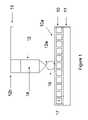
- FIG. 1illustrates an electrophoretic display of the present invention which comprises a stationary electrode layer ( 11 ), an electrophoretic display panel ( 10 ) comprising display cells ( 17 ), a movable element ( 12 ) having a conductive tip and a non-conductive liquid ( 14 ) filled in the body of the movable element.
- One side of the display panelhas a dielectric surface ( 10 a ).
- the liquid released from the movable element in the form of dropletscauses contact between the electrophoretic display panel ( 10 ) and the conductive tip of the movable element ( 12 ) which in turn forms a temporary yet an integrated electrical field between the stationary electrode layer ( 11 ) and the conductive tip of the movable element ( 12 ).
- the movable elementcomprises two parts 12 a and 12 b .
- the part, 12 aas stated, is conductive and is connected to a voltage source (not shown).
- the other part, 12 bmay be linked to a robotic arm ( 15 ) which controls the movement of the movable element
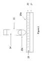
- FIG. 2illustrates an alternative design of the present invention.
- the movable element ( 22 )is configured into the shape of a ball point pen.
- the rolling ball ( 22 a ) at the tip of the pen-shape movable element ( 22 )is conductive and is connected to a voltage source (not shown).
- the internal liquid reservoir of the pen-shaped movable elementis filled with a non-conductive liquid ( 24 ).
- the rotation of the conductive rolling ball ( 22 a )causes the release of the non-conductive liquid onto the dielectric surface ( 20 a ) of the electrophoretic display panel ( 20 ) comprising display cells ( 25 ) to create contact between the conductive surface of the pen-shaped movable element and the electrophoretic display panel.
- An electric fieldis thus generated between the stationary electrode layer ( 21 ) and the conductive surface of the pen-shaped movable element ( 22 ).
- an electric signaltriggers the release of a predetermined amount of the non-conductive liquid ( 14 ) from the conductive tip of ( 12 a ) of the movable element.
- the distance between the conductive end ( 12 a ) of the movable element and the dielectric surface of the electrophoretic display panelmay be controlled to be less than the size of the non-conductive liquid droplet released.
- the droplet ( 16 ) of the non-conductive liquid releasedwill come in contact with both the conductive tip of the movable element ( 12 ) and the dielectric surface of the electrophoretic display panel ( 10 ).
- the voltage difference between the stationary electrode layer ( 11 ) and the conductive tip of the movable element ( 12 )forms an electric field sufficient to drive the charged pigment particles in the electrophoretic display panel.
- the droplet of the non-conductive liquidcan be deposited on the spot where the droplet is released.
- the dropletmay be withdrawn back into the movable element after the contact is no longer necessary.
- Suitable non-conductive liquids for the purpose of the present inventionmay be organic fluids that have a high dielectric constant (preferably higher than 5), are incompatible with the dielectric layer, have a reasonable evaporation time if needed, and are non-hazardous to environment at the application dosage.
- the non-conductive fluidsinclude, but are not limited to, deionized (DI) water and organic liquids, such as isopropanol and other alcoholic liquids, glycerin or liquids from the propylene glycol monomethyl ether acetate family. Among them, the deionized water and isopropyl alcohol are the more preferred.
- the movable elementmay also be configured into the shape of a fountain pen, with the tip of the fountain pen-shaped movable element being conductive and connected to a voltage source.
- a calligraphy brash with thin conductive copper wires that are connected to a voltage sourcemay also be used as a movable element to address such an electrophoretic display.
- the non-conductive fluidcan be placed aside separately in an ink fountain or reservoir.
- FIG. 3illustrates another alternative design.
- the movable element ( 32 )has a tip fixture ( 32 a ).
- the tip fixturecomprises a dry erasable marker head ( 33 ) with conductive wires embodied inside.
- the dry erasable marker head ( 33 )is preferably formed of a felt material or absorbent foam material.
- the non-conductive liquid ( 34 )is filled in the body (i.e., reservoir) of the movable element ( 32 ), which body is also preferably formed of a felt material or absorbent foam material.
- the liquidis applied to the dielectric surface ( 30 a ) of an electrophoretic display panel ( 30 ) comprising display cells ( 36 ) through the conductive head ( 33 ). Because of the capillary effect of the felt material, the liquid may be continuously drawn and replenished from the reservoir of the movable element through the conductive marker head to be applied to the dielectric surface of the electrophoretic display panel ( 30 ). An electric field thus is generated between the stationary electrode layer ( 31 ) and the conductive marker head of the movable element ( 32 ).
- the tip fixture ( 32 a )may be spring loaded ( 35 ) as shown.
- the conductive marker headneeds to be in contact with the dielectric surface of the display panel.
- spring(s) ( 35 )are used to better control the contact pressure.
- FIG. 4illustrates a further alternative design.
- a movable inkjet printeris used to address the electrophoretic display.
- the display panel ( 40 )comprising display cells ( 46 ) has a dielectric surface ( 40 a ) and a stationary electrode layer ( 41 ).
- the piezo inkjet nozzles ( 43 )are filled with the non-conductive liquid ( 44 ).
- the tips ( 43 a ) of the nozzles ( 43 )are conductive and are connected to a voltage source.
- the nozzles ( 43 )are placed at a predetermined distance from the electrophoretic display panel. The distance between the tips of the nozzles and the display panel is shorter than the vertical diameter of the droplet of the non-conductive liquid released.
- the droplet ( 45 )is in contact with the dielectric surface of the electrophoretic display panel ( 40 ), thus forming the necessary electrical field between the stationary electrode layer ( 41 ) and the conductive tip of the nozzles to cause particle movement in the electrophoretic display panel at the area of contact.
- FIG. 5illustrates an alternative method of using inkjet printing to address an electrophoretic display.
- the electrophoretic displayin this case, has a common electrode layer ( 52 ), an electrophoretic display panel ( 50 ) comprising display cells ( 56 ) and a stationary electrode ( 51 ).
- the stationary electrode layer ( 51 )has patterned openings ( 53 ).
- the common electrode layer ( 52 ) and the stationary electrode ( 51 )are connected to different polarities of the same voltage source.
- the stationary electrode ( 51 )comprises a first insulating layer ( 51 a ), a conductive layer ( 51 b ) and a second insulating layer ( 51 c ).
- One of the insulating layers ( 51 a )is in contact with the electrophoretic display panel ( 50 ) as shown in FIG. 5 .
- the insulating layer ( 51 a ) in contact with the electrophoretic display panel and the air inside the openings ( 53 )would keep the electrical circuit open.
- the reservoir (e.g., inkjet nozzle) ( 55 )dispenses the non-conductive liquid ( 54 ) into the openings
- the liquidin contact with the surface of the electrophoretic display panel and the conductive layer ( 51 b ) in the stationary electrode, forms an electric field path between the inkjet nozzle and the common electrode layer ( 52 ).
- the electric field formedcauses movement of the charged pigment particles in the electrophoretic display panel to form an image.
- the conductive layermay be formed of a metal wire mesh or thin copper foil and the openings may be formed by means of punching, laser cutting or the like.
- the writing sidecan be either the viewing side or the non-viewing side. If the stationary electrode ( 51 ) is non-transparent, the writing may be performed on this non-viewing side. However, if the stationary electrode ( 51 ) is transparent, the side of the stationary electrode may be the viewing side and the writing is then performed on the viewing side. This also applies to other designs of the present invention. In other words, the present invention provides the flexibility that the writing can be performed on either the viewing side or the non-viewing side.
Landscapes
- Physics & Mathematics (AREA)
- Nonlinear Science (AREA)
- Health & Medical Sciences (AREA)
- Life Sciences & Earth Sciences (AREA)
- Chemical & Material Sciences (AREA)
- Chemical Kinetics & Catalysis (AREA)
- Electrochemistry (AREA)
- Molecular Biology (AREA)
- General Physics & Mathematics (AREA)
- Optics & Photonics (AREA)
- Electrochromic Elements, Electrophoresis, Or Variable Reflection Or Absorption Elements (AREA)
- Devices For Indicating Variable Information By Combining Individual Elements (AREA)
Abstract
Description
Claims (17)
Priority Applications (1)
| Application Number | Priority Date | Filing Date | Title |
|---|---|---|---|
| US11/528,714US7408699B2 (en) | 2005-09-28 | 2006-09-26 | Electrophoretic display and methods of addressing such display |
Applications Claiming Priority (2)
| Application Number | Priority Date | Filing Date | Title |
|---|---|---|---|
| US72185905P | 2005-09-28 | 2005-09-28 | |
| US11/528,714US7408699B2 (en) | 2005-09-28 | 2006-09-26 | Electrophoretic display and methods of addressing such display |
Publications (2)
| Publication Number | Publication Date |
|---|---|
| US20070076289A1 US20070076289A1 (en) | 2007-04-05 |
| US7408699B2true US7408699B2 (en) | 2008-08-05 |
Family
ID=38029155
Family Applications (1)
| Application Number | Title | Priority Date | Filing Date |
|---|---|---|---|
| US11/528,714Active2026-11-03US7408699B2 (en) | 2005-09-28 | 2006-09-26 | Electrophoretic display and methods of addressing such display |
Country Status (2)
| Country | Link |
|---|---|
| US (1) | US7408699B2 (en) |
| JP (1) | JP2007102214A (en) |
Cited By (86)
| Publication number | Priority date | Publication date | Assignee | Title |
|---|---|---|---|---|
| US20100245981A1 (en)* | 2009-03-26 | 2010-09-30 | Jong-Souk Yeo | Electro-optical display |
| US7957054B1 (en) | 2009-12-21 | 2011-06-07 | Hewlett-Packard Development Company, L.P. | Electro-optical display systems |
| US20110149376A1 (en)* | 2009-12-21 | 2011-06-23 | Mabeck Jeffrey T | Electro-optical display systems |
| US20130003162A1 (en)* | 2011-06-29 | 2013-01-03 | Napoleon Leoni | Electronic paper with porous standoff layer |
| WO2017049020A1 (en) | 2015-09-16 | 2017-03-23 | E Ink Corporation | Apparatus and methods for driving displays |
| US10062337B2 (en) | 2015-10-12 | 2018-08-28 | E Ink California, Llc | Electrophoretic display device |
| WO2018164942A1 (en) | 2017-03-06 | 2018-09-13 | E Ink Corporation | Method for rendering color images |
| US10115354B2 (en) | 2009-09-15 | 2018-10-30 | E Ink California, Llc | Display controller system |
| US10163406B2 (en) | 2015-02-04 | 2018-12-25 | E Ink Corporation | Electro-optic displays displaying in dark mode and light mode, and related apparatus and methods |
| US10270939B2 (en) | 2016-05-24 | 2019-04-23 | E Ink Corporation | Method for rendering color images |
| US10276109B2 (en) | 2016-03-09 | 2019-04-30 | E Ink Corporation | Method for driving electro-optic displays |
| WO2019144097A1 (en) | 2018-01-22 | 2019-07-25 | E Ink Corporation | Electro-optic displays, and methods for driving same |
| US10380931B2 (en) | 2013-10-07 | 2019-08-13 | E Ink California, Llc | Driving methods for color display device |
| US10388233B2 (en) | 2015-08-31 | 2019-08-20 | E Ink Corporation | Devices and techniques for electronically erasing a drawing device |
| US10538111B2 (en) | 2010-06-02 | 2020-01-21 | Hewlett-Packard Development Company, L.P. | Writing electronic paper |
| WO2020018508A1 (en) | 2018-07-17 | 2020-01-23 | E Ink California, Llc | Electro-optic displays and driving methods |
| WO2020033175A1 (en) | 2018-08-10 | 2020-02-13 | E Ink California, Llc | Switchable light-collimating layer including bistable electrophoretic fluid |
| WO2020033787A1 (en) | 2018-08-10 | 2020-02-13 | E Ink California, Llc | Driving waveforms for switchable light-collimating layer including bistable electrophoretic fluid |
| US10573257B2 (en) | 2017-05-30 | 2020-02-25 | E Ink Corporation | Electro-optic displays |
| US10593272B2 (en) | 2016-03-09 | 2020-03-17 | E Ink Corporation | Drivers providing DC-balanced refresh sequences for color electrophoretic displays |
| US10726760B2 (en) | 2013-10-07 | 2020-07-28 | E Ink California, Llc | Driving methods to produce a mixed color state for an electrophoretic display |
| US10795233B2 (en) | 2015-11-18 | 2020-10-06 | E Ink Corporation | Electro-optic displays |
| US10803813B2 (en) | 2015-09-16 | 2020-10-13 | E Ink Corporation | Apparatus and methods for driving displays |
| US10832622B2 (en) | 2017-04-04 | 2020-11-10 | E Ink Corporation | Methods for driving electro-optic displays |
| US10882042B2 (en) | 2017-10-18 | 2021-01-05 | E Ink Corporation | Digital microfluidic devices including dual substrates with thin-film transistors and capacitive sensing |
| US11004409B2 (en) | 2013-10-07 | 2021-05-11 | E Ink California, Llc | Driving methods for color display device |
| US11062663B2 (en) | 2018-11-30 | 2021-07-13 | E Ink California, Llc | Electro-optic displays and driving methods |
| US11087644B2 (en) | 2015-08-19 | 2021-08-10 | E Ink Corporation | Displays intended for use in architectural applications |
| US11181799B2 (en) | 2018-05-17 | 2021-11-23 | E Ink California, Llc | Piezo electrophoretic display |
| US11249367B2 (en) | 2018-11-30 | 2022-02-15 | E Ink Corporation | Pressure-sensitive writing media comprising electrophoretic materials |
| US11257445B2 (en) | 2019-11-18 | 2022-02-22 | E Ink Corporation | Methods for driving electro-optic displays |
| US11289036B2 (en) | 2019-11-14 | 2022-03-29 | E Ink Corporation | Methods for driving electro-optic displays |
| US11314098B2 (en) | 2018-08-10 | 2022-04-26 | E Ink California, Llc | Switchable light-collimating layer with reflector |
| US11353759B2 (en) | 2018-09-17 | 2022-06-07 | Nuclera Nucleics Ltd. | Backplanes with hexagonal and triangular electrodes |
| US11404013B2 (en) | 2017-05-30 | 2022-08-02 | E Ink Corporation | Electro-optic displays with resistors for discharging remnant charges |
| US11422427B2 (en) | 2017-12-19 | 2022-08-23 | E Ink Corporation | Applications of electro-optic displays |
| US11423852B2 (en) | 2017-09-12 | 2022-08-23 | E Ink Corporation | Methods for driving electro-optic displays |
| US11450262B2 (en) | 2020-10-01 | 2022-09-20 | E Ink Corporation | Electro-optic displays, and methods for driving same |
| US11493821B2 (en) | 2018-08-14 | 2022-11-08 | E Ink California, Llc | Piezo electrophoretic display |
| US11511096B2 (en) | 2018-10-15 | 2022-11-29 | E Ink Corporation | Digital microfluidic delivery device |
| US11520202B2 (en) | 2020-06-11 | 2022-12-06 | E Ink Corporation | Electro-optic displays, and methods for driving same |
| US11568786B2 (en) | 2020-05-31 | 2023-01-31 | E Ink Corporation | Electro-optic displays, and methods for driving same |
| WO2023043714A1 (en) | 2021-09-14 | 2023-03-23 | E Ink Corporation | Coordinated top electrode - drive electrode voltages for switching optical state of electrophoretic displays using positive and negative voltages of different magnitudes |
| US11620959B2 (en) | 2020-11-02 | 2023-04-04 | E Ink Corporation | Enhanced push-pull (EPP) waveforms for achieving primary color sets in multi-color electrophoretic displays |
| US11644732B2 (en) | 2014-01-31 | 2023-05-09 | Hewlett-Packard Development Company, L.P. | Display device |
| US11657774B2 (en) | 2015-09-16 | 2023-05-23 | E Ink Corporation | Apparatus and methods for driving displays |
| US11657772B2 (en) | 2020-12-08 | 2023-05-23 | E Ink Corporation | Methods for driving electro-optic displays |
| US11686989B2 (en) | 2020-09-15 | 2023-06-27 | E Ink Corporation | Four particle electrophoretic medium providing fast, high-contrast optical state switching |
| WO2023122142A1 (en) | 2021-12-22 | 2023-06-29 | E Ink Corporation | Methods for driving electro-optic displays |
| WO2023129533A1 (en) | 2021-12-27 | 2023-07-06 | E Ink Corporation | Methods for measuring electrical properties of electro-optic displays |
| WO2023129692A1 (en) | 2021-12-30 | 2023-07-06 | E Ink California, Llc | Methods for driving electro-optic displays |
| WO2023132958A1 (en) | 2022-01-04 | 2023-07-13 | E Ink Corporation | Electrophoretic media comprising electrophoretic particles and a combination of charge control agents |
| US11721295B2 (en) | 2017-09-12 | 2023-08-08 | E Ink Corporation | Electro-optic displays, and methods for driving same |
| US11721296B2 (en) | 2020-11-02 | 2023-08-08 | E Ink Corporation | Method and apparatus for rendering color images |
| US11756494B2 (en) | 2020-11-02 | 2023-09-12 | E Ink Corporation | Driving sequences to remove prior state information from color electrophoretic displays |
| US11776496B2 (en) | 2020-09-15 | 2023-10-03 | E Ink Corporation | Driving voltages for advanced color electrophoretic displays and displays with improved driving voltages |
| WO2023211867A1 (en) | 2022-04-27 | 2023-11-02 | E Ink Corporation | Color displays configured to convert rgb image data for display on advanced color electronic paper |
| US11830448B2 (en) | 2021-11-04 | 2023-11-28 | E Ink Corporation | Methods for driving electro-optic displays |
| US11846863B2 (en) | 2020-09-15 | 2023-12-19 | E Ink Corporation | Coordinated top electrode—drive electrode voltages for switching optical state of electrophoretic displays using positive and negative voltages of different magnitudes |
| US11869451B2 (en) | 2021-11-05 | 2024-01-09 | E Ink Corporation | Multi-primary display mask-based dithering with low blooming sensitivity |
| WO2024044119A1 (en) | 2022-08-25 | 2024-02-29 | E Ink Corporation | Transitional driving modes for impulse balancing when switching between global color mode and direct update mode for electrophoretic displays |
| US11922893B2 (en) | 2021-12-22 | 2024-03-05 | E Ink Corporation | High voltage driving using top plane switching with zero voltage frames between driving frames |
| US11935495B2 (en) | 2021-08-18 | 2024-03-19 | E Ink Corporation | Methods for driving electro-optic displays |
| WO2024091547A1 (en) | 2022-10-25 | 2024-05-02 | E Ink Corporation | Methods for driving electro-optic displays |
| WO2024158855A1 (en) | 2023-01-27 | 2024-08-02 | E Ink Corporation | Multi-element pixel electrode circuits for electro-optic displays and methods for driving the same |
| WO2024182264A1 (en) | 2023-02-28 | 2024-09-06 | E Ink Corporation | Drive scheme for improved color gamut in color electrophoretic displays |
| US12125449B2 (en) | 2021-02-09 | 2024-10-22 | E Ink Corporation | Continuous waveform driving in multi-color electrophoretic displays |
| WO2024253934A1 (en) | 2023-06-05 | 2024-12-12 | E Ink Corporation | Color electrophoretic medium having four pigment particle system addressable by waveforms having four voltage levels |
| US12181767B2 (en) | 2020-09-15 | 2024-12-31 | E Ink Corporation | Five-particle electrophoretic medium with improved black optical state |
| WO2025006476A1 (en) | 2023-06-27 | 2025-01-02 | E Ink Corporation | Multi-particle electrophoretic display having low-flash image updates |
| WO2025006440A1 (en) | 2023-06-27 | 2025-01-02 | E Ink Corporation | Time-shifted waveforms for multi-particle electrophoretic displays providing low-flash image updates |
| WO2025006130A1 (en) | 2023-06-27 | 2025-01-02 | E Ink Corporation | Electrophoretic device with ambient light sensor and adaptive whiteness restoring and color balancing frontlight |
| US12190730B2 (en) | 2022-02-28 | 2025-01-07 | E Ink Corporation | Parking space management system |
| WO2025034396A1 (en) | 2023-08-08 | 2025-02-13 | E Ink Corporation | Backplanes for segmented electro-optic displays and methods of manufacturing same |
| WO2025076061A1 (en) | 2023-10-05 | 2025-04-10 | E Ink Corporation | Staged gate voltage control |
| WO2025096100A1 (en) | 2023-10-31 | 2025-05-08 | E Ink Corporation | Reflective display and projected capacitive touch sensor with shared transparent electrode |
| WO2025122853A1 (en) | 2023-12-06 | 2025-06-12 | E Ink Corporation | Method of driving a color electophoretic display to form images without dithering |
| WO2025128843A1 (en) | 2023-12-15 | 2025-06-19 | E Ink Corporation | Fast response color waveforms for multiparticle electrophoretic displays |
| US12339559B1 (en) | 2021-12-09 | 2025-06-24 | E Ink Corporation | Electro-optic displays and methods for discharging remnant voltage using backlight |
| WO2025136446A1 (en) | 2023-12-22 | 2025-06-26 | E Ink Corporation | Five-particle electrophoretic medium with improved black optical state |
| WO2025147504A1 (en) | 2024-01-05 | 2025-07-10 | E Ink Corporation | An electrophoretic medium comprising particles having a pigment core and a polymeric shell |
| WO2025147410A2 (en) | 2024-01-02 | 2025-07-10 | E Ink Corporation | Electrophoretic media comprising a cationic charge control agent |
| WO2025151355A1 (en) | 2024-01-08 | 2025-07-17 | E Ink Corporation | Electrophoretic device having an adhesive layer comprising conductive filler particles and a polymeric dispersant |
| WO2025155697A1 (en) | 2024-01-20 | 2025-07-24 | E Ink Corporation | Methods for delivering low-ghosting partial updates in color electrophoretic displays |
| WO2025155412A1 (en) | 2024-01-19 | 2025-07-24 | E Ink Corporation | Flexible segmented electro-optic displays and methods of manufacture |
| WO2025160290A1 (en) | 2024-01-24 | 2025-07-31 | E Ink Corporation | Improved methods for producing full-color epaper images with low grain |
Families Citing this family (2)
| Publication number | Priority date | Publication date | Assignee | Title |
|---|---|---|---|---|
| JP4720547B2 (en)* | 2006-03-07 | 2011-07-13 | 株式会社日立製作所 | Image display device |
| JP6510055B2 (en)* | 2015-02-18 | 2019-05-08 | イー インク コーポレイション | Addressable Electro-Optical Display |
Citations (9)
| Publication number | Priority date | Publication date | Assignee | Title |
|---|---|---|---|---|
| US4639720A (en)* | 1981-01-12 | 1987-01-27 | Harris Corporation | Electronic sketch pad |
| US5930026A (en) | 1996-10-25 | 1999-07-27 | Massachusetts Institute Of Technology | Nonemissive displays and piezoelectric power supplies therefor |
| US5961804A (en) | 1997-03-18 | 1999-10-05 | Massachusetts Institute Of Technology | Microencapsulated electrophoretic display |
| US6473072B1 (en)* | 1998-05-12 | 2002-10-29 | E Ink Corporation | Microencapsulated electrophoretic electrostatically-addressed media for drawing device applications |
| US6506438B2 (en)* | 1998-12-15 | 2003-01-14 | E Ink Corporation | Method for printing of transistor arrays on plastic substrates |
| US6672921B1 (en) | 2000-03-03 | 2004-01-06 | Sipix Imaging, Inc. | Manufacturing process for electrophoretic display |
| US20040182711A1 (en) | 2003-01-30 | 2004-09-23 | Rong-Chang Liang | High performance capsules for electrophoretic displays |
| US6930818B1 (en) | 2000-03-03 | 2005-08-16 | Sipix Imaging, Inc. | Electrophoretic display and novel process for its manufacture |
| US6933098B2 (en) | 2000-01-11 | 2005-08-23 | Sipix Imaging Inc. | Process for roll-to-roll manufacture of a display by synchronized photolithographic exposure on a substrate web |
- 2006
- 2006-09-26USUS11/528,714patent/US7408699B2/enactiveActive
- 2006-09-27JPJP2006261894Apatent/JP2007102214A/enactivePending
Patent Citations (10)
| Publication number | Priority date | Publication date | Assignee | Title |
|---|---|---|---|---|
| US4639720A (en)* | 1981-01-12 | 1987-01-27 | Harris Corporation | Electronic sketch pad |
| US5930026A (en) | 1996-10-25 | 1999-07-27 | Massachusetts Institute Of Technology | Nonemissive displays and piezoelectric power supplies therefor |
| US5961804A (en) | 1997-03-18 | 1999-10-05 | Massachusetts Institute Of Technology | Microencapsulated electrophoretic display |
| US6473072B1 (en)* | 1998-05-12 | 2002-10-29 | E Ink Corporation | Microencapsulated electrophoretic electrostatically-addressed media for drawing device applications |
| US6738050B2 (en)* | 1998-05-12 | 2004-05-18 | E Ink Corporation | Microencapsulated electrophoretic electrostatically addressed media for drawing device applications |
| US6506438B2 (en)* | 1998-12-15 | 2003-01-14 | E Ink Corporation | Method for printing of transistor arrays on plastic substrates |
| US6933098B2 (en) | 2000-01-11 | 2005-08-23 | Sipix Imaging Inc. | Process for roll-to-roll manufacture of a display by synchronized photolithographic exposure on a substrate web |
| US6672921B1 (en) | 2000-03-03 | 2004-01-06 | Sipix Imaging, Inc. | Manufacturing process for electrophoretic display |
| US6930818B1 (en) | 2000-03-03 | 2005-08-16 | Sipix Imaging, Inc. | Electrophoretic display and novel process for its manufacture |
| US20040182711A1 (en) | 2003-01-30 | 2004-09-23 | Rong-Chang Liang | High performance capsules for electrophoretic displays |
Non-Patent Citations (36)
| Title |
|---|
| Allen, K. (Oct. 2003). Electrophoretics Fulfilled. Emerging Displays Review: Emerging Display Technologies, Monthly Report-Oct. 2003, 9-14. |
| Bardsley, J.N. & Pinnel, M.R. (Nov. 2004) Microcup(TM) Electrophoretic Displays. USDC Flexible Display Report, 3.1.2. pp. 3-12-3-16. |
| Chaug, Y.S., Haubrich, J.E., Sereda, M. and Liang, R.C. (Apr. 2004). Roll-to-Roll Processes for the Manufacturing of Patterned Conductive Electrodes on Flexible Substrates. Mat. Res. Soc. Symp. Proc., vol. 814, l9.6.1. |
| Chen, S.M. (Jul. 2003) The Applications for the Revolutionary Electronic Paper Technology. OPTO News & Letters, 102, 37-41. (in Chinese, English abstract attached, full translation available upon request). |
| Chen, S.M. (May 2003) The New Applications and the Dynamics of Companies. TRI. 1-10. (In Chinese, English abstract attached, full translation available upon request). |
| Chiang, et al (1979) A Stylus Writable Electrophophoretic Display Device. SID Digest, pp. 44-45. |
| Chung, J., Hou, J., Wang, W., Chu, L.Y., Yao, W., & Liang, R.C. (Dec. 2003). Microcup(R) Electrophoretic Displays, Grayscale and Color Rendition. IDW, AMD2/EP1-2, 243-246. |
| Ho, C.,& Liang, R.C. (Dec. 2003). Microcup (R) Electronic Paper by Roll-to-Roll Manufacturing Processes. Presentation conducted at FEG, Nei-Li, Taiwan. |
| Ho, Candice. (Feb. 1, 2005) Microcupt(R) Electronic Paper Device and Applicaiton. Presentation conducted at USDC 4th Annual Flexible Display Conference 2005. |
| Hopper, M. A. et al, "An Electrophoretic Display, its Properties, Model and Addressing", IEEE Transactions on Electron Devices, 26(8): 1148-1152 (1979). |
| Hou, J., Chen, Y., Li, Y., Weng, X., Li, H. And Pereira, C. (May 2004). Reliability and Performance of Flexible Electrophoretic Display by Roll-to-Roll Manufacturing Processes. SID Digest, 32.3, 1066-1069. |
| Lee, H., & Liang, R.C. (Jun. 2003) SiPix Microcup(R) Electronic Paper-An Introduction. Advanced Display, Issue 37, 4-9 (in Chinese, English abstract attached, full translation available upon request). |
| Liang, R.C. (Apr. 2004). Microcup Electronic Paper by Roll-to-Roll Manufacturing Process. Presentation at the Flexible Displays & Electronics 2004 of Intertech, San Fransisco, California, USA. |
| Liang, R.C. (Feb. 2003) Microcup(R) Electrophoretic and Liquid Crystal Displays by Roll-to-Roll Manufacturing Processes. Presentation conducted at the Flexible Microelectronics & Displays Conference of U.S. Display Consortium, Phoenix, Arizona, USA. |
| Liang, R.C. (Oct. 2004) Flexible and Roll-able Display/Electronic Paper-A Technology Overview. Paper presented at the METS 2004 Conference in Taipie, Taiwan. |
| Liang, R.C., & Tseng, S. (Feb. 2003). Microcup(R) LCD, An New Type of Dispersed LCD by A Roll-to-Roll Manufacturing Process. Paper presented at the IDMC, Taipei, Taiwan. |
| Liang, R.C., (Feb. 2005) Flexible and Roll-able Displays/Electronic Paper-A Brief Technology Overview. Flexible Display Forum, 2005, Taiwan. |
| Liang, R.C., Hou, J., & Zang, H.M. (Dec. 2002) Microcup Electrophoretic Displays by Roll-to-Roll Manufacturing Processes. IDW, EP2-2, 1337-1340. |
| Liang, R.C., Hou, J., & Zang, H.M., & Chung, J. (Feb. 2003). Passive Matrix Microcup(R) Electrophoretic Displays. Paper presented at the IDMC, Taipei, Taiwan. |
| Liang, R.C., Hou, J., Chung, J., Wang, X., Pereira, C., & Chen, Y. (2003). Microcup(R) Active and Passive Matrix Electrophoretic Displays by A Roll-to-Roll Manufacturing Processes. SID Digest, 20.1. |
| Liang, R.C., Hou, J., Zang, H.M., Chung, J., & Tseng, S. (2003). Microcup(R) displays : Electronic Paper by Roll-to-Roll Manufacturing Processes. Journal of the SID, 11(4), 621-628. |
| Liang, R.C., Zang, H.M., Wang, X., Chung, J. & Lee, H., (Jun./Jul. 2004) "Format Flexible Microcup (R) Electronic Paper by Roll-to-Roll Manufacturing Process", Presentation conducted at the 14th FPD Manufacturing Technology EXPO & Conference. |
| Mossman, M.A. et al (2001) New Reflective Display Based on Total Internal Reflection in Prismatic Microstructure. SID IDRC Proceedings, pp. 311. |
| Mossman, M.A., et al (2001) New Reflective Color Display Techniques Based on Total Internal Reflection and Subtractive Color Filtering. SID 01 Digest, pp. 1054, (2001). |
| Mossman, M.A., et al. (2002) Grey Scale Control of TIR Using Electrophoresis of Sub-Optical Pigment Particles, SID 02 Digest, pp. 522. |
| Nikkei Microdevices. (Dec. 2002) Newly-Developed Color Electronic Paper Promises-Unbeatable Production Efficiency. Nikkei Microdevices, 3. (in Japanese, with English translation). |
| Wang, X., Kiluk, S., Chang, C., & Liang, R.C. (Feb. 2004). Mirocup (R) Electronic Paper and the Converting Processes. ASID, 10.1.2-26, 396-399, Nanjing, China. |
| Wang, X., Kiluk, S., Chang, C., & Liang, R.C., (Jun. 2004) Microcup(R) Electronic Paper and the Converting Processes. Advanced Display, Issue 43, 48-51. |
| Wang, X., Li, P., Sodhi, D., Xu, T. and Bruner, S. et al., (Feb. 2006) Inkjet Fabrication of Multi-Color Microcup(R) Electrophorectic Display. the Flexible Microelectronics & Displays Conference of U.S. Display Consortium. |
| Wang, X., Zang, HM., and Li, P. (Jun. 2006) Roll-to-Roll Manufacturing Process for Full Color Electrophoretic film. SID Digest, pp. 1587-1589. |
| Zang, H.M, Hwang, J.J., Gu, H., Hou, J., Weng, X., Chen, Y., et al. (Jan. 2004). Threshold and Grayscale Stability of Microcup (R) Electronic Paper. Proceeding of SPIE-IS&T Electronic Imaging, SPIE vol. 5289, 102-108. |
| Zang, H.M. (Feb. 2004). Microcup Electronic Paper. Presentation conducted at the Displays & Microelectronics Conference of U.S. Display Consortium, Phoenix, Arizona, USA. |
| Zang, H.M. (Oct. 2003). Microcup (R) Electronic Paper by Roll-to-Roll Manufacturing Processes. Presentation conducted at the Advisory Board Meeting, Bowling Green State University, Ohio, USA. |
| Zang, H.M., & Liang, R.C. (2003) Microcup Electronic Paper by Roll-to-Roll Manufacturing Processes. The Spectrum, 16(2), 16-21. |
| Zang, H.M.Hou, Jack, (Feb. 2005) Flexible Microcup(R) EPD by RTR Process. Presentation conducted at 2<SUP>nd </SUP>Annual Paper-Like Displays Conference, Feb. 9-11, 2005, St. Pete Beach, Florida. |
| Zang, HM., Wang, W., Sun, C., Gu, H., and Chen, Y. (May 2006) Monochrome and Area Color Microcup(R) EPDs by Roll-to-Roll Manufacturing Processes. ICIS ' 06 International Congress of Imaging Science Final Program and Proceedings, pp. 362-365. |
Cited By (147)
| Publication number | Priority date | Publication date | Assignee | Title |
|---|---|---|---|---|
| US8018642B2 (en) | 2009-03-26 | 2011-09-13 | Hewlett-Packard Development Company, L.P. | Electro-optical display |
| US20100245981A1 (en)* | 2009-03-26 | 2010-09-30 | Jong-Souk Yeo | Electro-optical display |
| US10115354B2 (en) | 2009-09-15 | 2018-10-30 | E Ink California, Llc | Display controller system |
| US7957054B1 (en) | 2009-12-21 | 2011-06-07 | Hewlett-Packard Development Company, L.P. | Electro-optical display systems |
| US20110149376A1 (en)* | 2009-12-21 | 2011-06-23 | Mabeck Jeffrey T | Electro-optical display systems |
| US8089687B2 (en) | 2009-12-21 | 2012-01-03 | Hewlett-Packard Development Company, L.P. | Electro-optical display systems |
| US10538111B2 (en) | 2010-06-02 | 2020-01-21 | Hewlett-Packard Development Company, L.P. | Writing electronic paper |
| US11390091B2 (en) | 2010-06-02 | 2022-07-19 | Hewlett-Packard Development Company, L.P. | Writing electronic paper |
| US9709870B2 (en) | 2011-06-29 | 2017-07-18 | Hewlett-Packard Development Company, L.P. | Electronic paper with porous standoff layer |
| US9104082B2 (en)* | 2011-06-29 | 2015-08-11 | Hewlett-Packard Development Company, L.P. | Electronic paper with porous standoff layer |
| US20130003162A1 (en)* | 2011-06-29 | 2013-01-03 | Napoleon Leoni | Electronic paper with porous standoff layer |
| US11217145B2 (en) | 2013-10-07 | 2022-01-04 | E Ink California, Llc | Driving methods to produce a mixed color state for an electrophoretic display |
| US11004409B2 (en) | 2013-10-07 | 2021-05-11 | E Ink California, Llc | Driving methods for color display device |
| US10726760B2 (en) | 2013-10-07 | 2020-07-28 | E Ink California, Llc | Driving methods to produce a mixed color state for an electrophoretic display |
| US10380931B2 (en) | 2013-10-07 | 2019-08-13 | E Ink California, Llc | Driving methods for color display device |
| US11644732B2 (en) | 2014-01-31 | 2023-05-09 | Hewlett-Packard Development Company, L.P. | Display device |
| US10163406B2 (en) | 2015-02-04 | 2018-12-25 | E Ink Corporation | Electro-optic displays displaying in dark mode and light mode, and related apparatus and methods |
| US11087644B2 (en) | 2015-08-19 | 2021-08-10 | E Ink Corporation | Displays intended for use in architectural applications |
| US10388233B2 (en) | 2015-08-31 | 2019-08-20 | E Ink Corporation | Devices and techniques for electronically erasing a drawing device |
| US10803813B2 (en) | 2015-09-16 | 2020-10-13 | E Ink Corporation | Apparatus and methods for driving displays |
| WO2017049020A1 (en) | 2015-09-16 | 2017-03-23 | E Ink Corporation | Apparatus and methods for driving displays |
| US11450286B2 (en) | 2015-09-16 | 2022-09-20 | E Ink Corporation | Apparatus and methods for driving displays |
| US11657774B2 (en) | 2015-09-16 | 2023-05-23 | E Ink Corporation | Apparatus and methods for driving displays |
| US10062337B2 (en) | 2015-10-12 | 2018-08-28 | E Ink California, Llc | Electrophoretic display device |
| US10795233B2 (en) | 2015-11-18 | 2020-10-06 | E Ink Corporation | Electro-optic displays |
| US11030965B2 (en) | 2016-03-09 | 2021-06-08 | E Ink Corporation | Drivers providing DC-balanced refresh sequences for color electrophoretic displays |
| US11404012B2 (en) | 2016-03-09 | 2022-08-02 | E Ink Corporation | Drivers providing DC-balanced refresh sequences for color electrophoretic displays |
| US10593272B2 (en) | 2016-03-09 | 2020-03-17 | E Ink Corporation | Drivers providing DC-balanced refresh sequences for color electrophoretic displays |
| US10276109B2 (en) | 2016-03-09 | 2019-04-30 | E Ink Corporation | Method for driving electro-optic displays |
| US11265443B2 (en) | 2016-05-24 | 2022-03-01 | E Ink Corporation | System for rendering color images |
| US10771652B2 (en) | 2016-05-24 | 2020-09-08 | E Ink Corporation | Method for rendering color images |
| US10270939B2 (en) | 2016-05-24 | 2019-04-23 | E Ink Corporation | Method for rendering color images |
| US10554854B2 (en) | 2016-05-24 | 2020-02-04 | E Ink Corporation | Method for rendering color images |
| WO2018164942A1 (en) | 2017-03-06 | 2018-09-13 | E Ink Corporation | Method for rendering color images |
| US11527216B2 (en) | 2017-03-06 | 2022-12-13 | E Ink Corporation | Method for rendering color images |
| US11094288B2 (en) | 2017-03-06 | 2021-08-17 | E Ink Corporation | Method and apparatus for rendering color images |
| US12100369B2 (en) | 2017-03-06 | 2024-09-24 | E Ink Corporation | Method for rendering color images |
| US10467984B2 (en) | 2017-03-06 | 2019-11-05 | E Ink Corporation | Method for rendering color images |
| US10832622B2 (en) | 2017-04-04 | 2020-11-10 | E Ink Corporation | Methods for driving electro-optic displays |
| US11398196B2 (en) | 2017-04-04 | 2022-07-26 | E Ink Corporation | Methods for driving electro-optic displays |
| US10825405B2 (en) | 2017-05-30 | 2020-11-03 | E Ink Corporatior | Electro-optic displays |
| US10573257B2 (en) | 2017-05-30 | 2020-02-25 | E Ink Corporation | Electro-optic displays |
| US11107425B2 (en) | 2017-05-30 | 2021-08-31 | E Ink Corporation | Electro-optic displays with resistors for discharging remnant charges |
| US11404013B2 (en) | 2017-05-30 | 2022-08-02 | E Ink Corporation | Electro-optic displays with resistors for discharging remnant charges |
| US11568827B2 (en) | 2017-09-12 | 2023-01-31 | E Ink Corporation | Methods for driving electro-optic displays to minimize edge ghosting |
| US11423852B2 (en) | 2017-09-12 | 2022-08-23 | E Ink Corporation | Methods for driving electro-optic displays |
| US11721295B2 (en) | 2017-09-12 | 2023-08-08 | E Ink Corporation | Electro-optic displays, and methods for driving same |
| US11935496B2 (en) | 2017-09-12 | 2024-03-19 | E Ink Corporation | Electro-optic displays, and methods for driving same |
| US10882042B2 (en) | 2017-10-18 | 2021-01-05 | E Ink Corporation | Digital microfluidic devices including dual substrates with thin-film transistors and capacitive sensing |
| US11422427B2 (en) | 2017-12-19 | 2022-08-23 | E Ink Corporation | Applications of electro-optic displays |
| US12130530B2 (en) | 2017-12-19 | 2024-10-29 | E Ink Corporation | Applications of electro-optic displays |
| WO2019144097A1 (en) | 2018-01-22 | 2019-07-25 | E Ink Corporation | Electro-optic displays, and methods for driving same |
| US11892740B2 (en) | 2018-05-17 | 2024-02-06 | E Ink Corporation | Piezo electrophoretic display |
| US12298645B2 (en) | 2018-05-17 | 2025-05-13 | E Ink Corporation | Piezo electrophoretic display |
| US11181799B2 (en) | 2018-05-17 | 2021-11-23 | E Ink California, Llc | Piezo electrophoretic display |
| US12253784B2 (en) | 2018-07-17 | 2025-03-18 | E Ink Corporation | Electro-optic displays and driving methods |
| WO2020018508A1 (en) | 2018-07-17 | 2020-01-23 | E Ink California, Llc | Electro-optic displays and driving methods |
| US11789330B2 (en) | 2018-07-17 | 2023-10-17 | E Ink California, Llc | Electro-optic displays and driving methods |
| US11314098B2 (en) | 2018-08-10 | 2022-04-26 | E Ink California, Llc | Switchable light-collimating layer with reflector |
| US11719953B2 (en) | 2018-08-10 | 2023-08-08 | E Ink California, Llc | Switchable light-collimating layer with reflector |
| WO2020033175A1 (en) | 2018-08-10 | 2020-02-13 | E Ink California, Llc | Switchable light-collimating layer including bistable electrophoretic fluid |
| WO2020033787A1 (en) | 2018-08-10 | 2020-02-13 | E Ink California, Llc | Driving waveforms for switchable light-collimating layer including bistable electrophoretic fluid |
| US11435606B2 (en) | 2018-08-10 | 2022-09-06 | E Ink California, Llc | Driving waveforms for switchable light-collimating layer including bistable electrophoretic fluid |
| US11656526B2 (en) | 2018-08-10 | 2023-05-23 | E Ink California, Llc | Switchable light-collimating layer including bistable electrophoretic fluid |
| US11397366B2 (en) | 2018-08-10 | 2022-07-26 | E Ink California, Llc | Switchable light-collimating layer including bistable electrophoretic fluid |
| US11493821B2 (en) | 2018-08-14 | 2022-11-08 | E Ink California, Llc | Piezo electrophoretic display |
| US11353759B2 (en) | 2018-09-17 | 2022-06-07 | Nuclera Nucleics Ltd. | Backplanes with hexagonal and triangular electrodes |
| US11511096B2 (en) | 2018-10-15 | 2022-11-29 | E Ink Corporation | Digital microfluidic delivery device |
| US12186514B2 (en) | 2018-10-15 | 2025-01-07 | E Ink Corporation | Digital microfluidic delivery device |
| US11380274B2 (en) | 2018-11-30 | 2022-07-05 | E Ink California, Llc | Electro-optic displays and driving methods |
| US12298647B2 (en) | 2018-11-30 | 2025-05-13 | E Ink Corporation | Pressure-sensitive writing media comprising electrophoretic materials |
| US11062663B2 (en) | 2018-11-30 | 2021-07-13 | E Ink California, Llc | Electro-optic displays and driving methods |
| US11249367B2 (en) | 2018-11-30 | 2022-02-15 | E Ink Corporation | Pressure-sensitive writing media comprising electrophoretic materials |
| US11735127B2 (en) | 2018-11-30 | 2023-08-22 | E Ink California, Llc | Electro-optic displays and driving methods |
| US11809057B2 (en) | 2018-11-30 | 2023-11-07 | E Ink Corporation | Pressure-sensitive writing media comprising electrophoretic materials |
| US11289036B2 (en) | 2019-11-14 | 2022-03-29 | E Ink Corporation | Methods for driving electro-optic displays |
| US11257445B2 (en) | 2019-11-18 | 2022-02-22 | E Ink Corporation | Methods for driving electro-optic displays |
| US11568786B2 (en) | 2020-05-31 | 2023-01-31 | E Ink Corporation | Electro-optic displays, and methods for driving same |
| US12347356B2 (en) | 2020-05-31 | 2025-07-01 | E Ink Corporation | Electro-optic displays, and methods for driving same |
| US11520202B2 (en) | 2020-06-11 | 2022-12-06 | E Ink Corporation | Electro-optic displays, and methods for driving same |
| US11948523B1 (en) | 2020-09-15 | 2024-04-02 | E Ink Corporation | Driving voltages for advanced color electrophoretic displays and displays with improved driving voltages |
| US12181767B2 (en) | 2020-09-15 | 2024-12-31 | E Ink Corporation | Five-particle electrophoretic medium with improved black optical state |
| US11686989B2 (en) | 2020-09-15 | 2023-06-27 | E Ink Corporation | Four particle electrophoretic medium providing fast, high-contrast optical state switching |
| US12361902B2 (en) | 2020-09-15 | 2025-07-15 | E Ink Corporation | Driving voltages for advanced color electrophoretic displays and displays with improved driving voltages |
| US11776496B2 (en) | 2020-09-15 | 2023-10-03 | E Ink Corporation | Driving voltages for advanced color electrophoretic displays and displays with improved driving voltages |
| US12197099B2 (en) | 2020-09-15 | 2025-01-14 | E Ink Corporation | Coordinated top electrode—drive electrode voltages for switching optical state of electrophoretic displays using positive and negative voltages of different magnitudes |
| US11837184B2 (en) | 2020-09-15 | 2023-12-05 | E Ink Corporation | Driving voltages for advanced color electrophoretic displays and displays with improved driving voltages |
| US11846863B2 (en) | 2020-09-15 | 2023-12-19 | E Ink Corporation | Coordinated top electrode—drive electrode voltages for switching optical state of electrophoretic displays using positive and negative voltages of different magnitudes |
| US12044945B2 (en) | 2020-09-15 | 2024-07-23 | E Ink Corporation | Four particle electrophoretic medium providing fast, high-contrast optical state switching |
| US11450262B2 (en) | 2020-10-01 | 2022-09-20 | E Ink Corporation | Electro-optic displays, and methods for driving same |
| US11721296B2 (en) | 2020-11-02 | 2023-08-08 | E Ink Corporation | Method and apparatus for rendering color images |
| US12347398B2 (en) | 2020-11-02 | 2025-07-01 | E Ink Corporation | Enhanced push-pull (EPP) waveforms for achieving primary color sets in multi-color electrophoretic displays |
| US11620959B2 (en) | 2020-11-02 | 2023-04-04 | E Ink Corporation | Enhanced push-pull (EPP) waveforms for achieving primary color sets in multi-color electrophoretic displays |
| US11756494B2 (en) | 2020-11-02 | 2023-09-12 | E Ink Corporation | Driving sequences to remove prior state information from color electrophoretic displays |
| US12087244B2 (en) | 2020-11-02 | 2024-09-10 | E Ink Corporation | Enhanced push-pull (EPP) waveforms for achieving primary color sets in multi-color electrophoretic displays |
| US11798506B2 (en) | 2020-11-02 | 2023-10-24 | E Ink Corporation | Enhanced push-pull (EPP) waveforms for achieving primary color sets in multi-color electrophoretic displays |
| US12307989B2 (en) | 2020-11-02 | 2025-05-20 | E Ink Corporation | Driving sequences to remove prior state information from color electrophoretic displays |
| US11657772B2 (en) | 2020-12-08 | 2023-05-23 | E Ink Corporation | Methods for driving electro-optic displays |
| US12125449B2 (en) | 2021-02-09 | 2024-10-22 | E Ink Corporation | Continuous waveform driving in multi-color electrophoretic displays |
| US12406632B2 (en) | 2021-02-09 | 2025-09-02 | E Ink Corporation | Continuous waveform driving in multi-color electrophoretic displays |
| US12131713B2 (en) | 2021-02-09 | 2024-10-29 | E Ink Corporation | Continuous waveform driving in multi-color electrophoretic displays |
| US11935495B2 (en) | 2021-08-18 | 2024-03-19 | E Ink Corporation | Methods for driving electro-optic displays |
| WO2023043714A1 (en) | 2021-09-14 | 2023-03-23 | E Ink Corporation | Coordinated top electrode - drive electrode voltages for switching optical state of electrophoretic displays using positive and negative voltages of different magnitudes |
| US11830448B2 (en) | 2021-11-04 | 2023-11-28 | E Ink Corporation | Methods for driving electro-optic displays |
| US11869451B2 (en) | 2021-11-05 | 2024-01-09 | E Ink Corporation | Multi-primary display mask-based dithering with low blooming sensitivity |
| US12249291B2 (en) | 2021-11-05 | 2025-03-11 | E Ink Corporation | Multi-primary display mask-based dithering with low blooming sensitivity |
| US12339559B1 (en) | 2021-12-09 | 2025-06-24 | E Ink Corporation | Electro-optic displays and methods for discharging remnant voltage using backlight |
| WO2023122142A1 (en) | 2021-12-22 | 2023-06-29 | E Ink Corporation | Methods for driving electro-optic displays |
| US11922893B2 (en) | 2021-12-22 | 2024-03-05 | E Ink Corporation | High voltage driving using top plane switching with zero voltage frames between driving frames |
| US12307988B2 (en) | 2021-12-22 | 2025-05-20 | E Ink Corporation | Methods for globally applying voltages to the display pixels of electro-optic displays |
| US12400611B2 (en) | 2021-12-22 | 2025-08-26 | E Ink Corporation | High voltage driving using top plane switching with zero voltage frames between driving frames |
| WO2023129533A1 (en) | 2021-12-27 | 2023-07-06 | E Ink Corporation | Methods for measuring electrical properties of electro-optic displays |
| US11854448B2 (en) | 2021-12-27 | 2023-12-26 | E Ink Corporation | Methods for measuring electrical properties of electro-optic displays |
| US12249262B2 (en) | 2021-12-27 | 2025-03-11 | E Ink Corporation | Methods for measuring electrical properties of electro-optic displays |
| US12085829B2 (en) | 2021-12-30 | 2024-09-10 | E Ink Corporation | Methods for driving electro-optic displays |
| WO2023129692A1 (en) | 2021-12-30 | 2023-07-06 | E Ink California, Llc | Methods for driving electro-optic displays |
| US12399411B2 (en) | 2021-12-30 | 2025-08-26 | E Ink Corporation | Electro-optic displays and driving methods |
| WO2023132958A1 (en) | 2022-01-04 | 2023-07-13 | E Ink Corporation | Electrophoretic media comprising electrophoretic particles and a combination of charge control agents |
| US12190730B2 (en) | 2022-02-28 | 2025-01-07 | E Ink Corporation | Parking space management system |
| WO2023211867A1 (en) | 2022-04-27 | 2023-11-02 | E Ink Corporation | Color displays configured to convert rgb image data for display on advanced color electronic paper |
| US11984088B2 (en) | 2022-04-27 | 2024-05-14 | E Ink Corporation | Color displays configured to convert RGB image data for display on advanced color electronic paper |
| US12334029B2 (en) | 2022-04-27 | 2025-06-17 | E Ink Corporation | Color displays configured to convert RGB image data for display on advanced color electronic paper |
| WO2024044119A1 (en) | 2022-08-25 | 2024-02-29 | E Ink Corporation | Transitional driving modes for impulse balancing when switching between global color mode and direct update mode for electrophoretic displays |
| WO2024091547A1 (en) | 2022-10-25 | 2024-05-02 | E Ink Corporation | Methods for driving electro-optic displays |
| WO2024158855A1 (en) | 2023-01-27 | 2024-08-02 | E Ink Corporation | Multi-element pixel electrode circuits for electro-optic displays and methods for driving the same |
| US12190836B2 (en) | 2023-01-27 | 2025-01-07 | E Ink Corporation | Multi-element pixel electrode circuits for electro-optic displays and methods for driving the same |
| WO2024182264A1 (en) | 2023-02-28 | 2024-09-06 | E Ink Corporation | Drive scheme for improved color gamut in color electrophoretic displays |
| US12272324B2 (en) | 2023-02-28 | 2025-04-08 | E Ink Corporation | Drive scheme for improved color gamut in color electrophoretic displays |
| WO2024253934A1 (en) | 2023-06-05 | 2024-12-12 | E Ink Corporation | Color electrophoretic medium having four pigment particle system addressable by waveforms having four voltage levels |
| US12394388B2 (en) | 2023-06-27 | 2025-08-19 | E Ink Corporation | Time-shifted waveforms for multi-particle electrophoretic displays providing low-flash image updates |
| US12412538B2 (en) | 2023-06-27 | 2025-09-09 | E Ink Corporation | Electrophoretic device with ambient light sensor and adaptive whiteness restoring and color balancing frontlight |
| WO2025006476A1 (en) | 2023-06-27 | 2025-01-02 | E Ink Corporation | Multi-particle electrophoretic display having low-flash image updates |
| WO2025006130A1 (en) | 2023-06-27 | 2025-01-02 | E Ink Corporation | Electrophoretic device with ambient light sensor and adaptive whiteness restoring and color balancing frontlight |
| US12406631B2 (en) | 2023-06-27 | 2025-09-02 | E Ink Corporation | Multi-particle electrophoretic display having low-flash image updates |
| WO2025006440A1 (en) | 2023-06-27 | 2025-01-02 | E Ink Corporation | Time-shifted waveforms for multi-particle electrophoretic displays providing low-flash image updates |
| WO2025034396A1 (en) | 2023-08-08 | 2025-02-13 | E Ink Corporation | Backplanes for segmented electro-optic displays and methods of manufacturing same |
| WO2025076061A1 (en) | 2023-10-05 | 2025-04-10 | E Ink Corporation | Staged gate voltage control |
| WO2025096100A1 (en) | 2023-10-31 | 2025-05-08 | E Ink Corporation | Reflective display and projected capacitive touch sensor with shared transparent electrode |
| WO2025122853A1 (en) | 2023-12-06 | 2025-06-12 | E Ink Corporation | Method of driving a color electophoretic display to form images without dithering |
| WO2025128843A1 (en) | 2023-12-15 | 2025-06-19 | E Ink Corporation | Fast response color waveforms for multiparticle electrophoretic displays |
| WO2025136446A1 (en) | 2023-12-22 | 2025-06-26 | E Ink Corporation | Five-particle electrophoretic medium with improved black optical state |
| WO2025147410A2 (en) | 2024-01-02 | 2025-07-10 | E Ink Corporation | Electrophoretic media comprising a cationic charge control agent |
| WO2025147504A1 (en) | 2024-01-05 | 2025-07-10 | E Ink Corporation | An electrophoretic medium comprising particles having a pigment core and a polymeric shell |
| WO2025151355A1 (en) | 2024-01-08 | 2025-07-17 | E Ink Corporation | Electrophoretic device having an adhesive layer comprising conductive filler particles and a polymeric dispersant |
| WO2025155412A1 (en) | 2024-01-19 | 2025-07-24 | E Ink Corporation | Flexible segmented electro-optic displays and methods of manufacture |
| WO2025155697A1 (en) | 2024-01-20 | 2025-07-24 | E Ink Corporation | Methods for delivering low-ghosting partial updates in color electrophoretic displays |
| WO2025160290A1 (en) | 2024-01-24 | 2025-07-31 | E Ink Corporation | Improved methods for producing full-color epaper images with low grain |
Also Published As
| Publication number | Publication date |
|---|---|
| JP2007102214A (en) | 2007-04-19 |
| US20070076289A1 (en) | 2007-04-05 |
Similar Documents
| Publication | Publication Date | Title |
|---|---|---|
| US7408699B2 (en) | Electrophoretic display and methods of addressing such display | |
| JP2007102214A5 (en) | ||
| US8643939B2 (en) | Electrophoretic display sheet and manufacturing method therefor | |
| US8144388B2 (en) | Display apparatus and display sheet | |
| US6639580B1 (en) | Electrophoretic display device and method for addressing display device | |
| US8031168B2 (en) | Display device having an electrode partially covering a picture element | |
| JP4416380B2 (en) | Electrophoretic display device and driving method thereof | |
| JP5501602B2 (en) | Display device | |
| US7999997B2 (en) | Electrophoretic display device, method of manufacturing electrophoretic display device, and electronic device | |
| JP3625421B2 (en) | Electrophoretic display device | |
| JP5620070B2 (en) | Electrochromic display device | |
| CN101506727A (en) | Electrophoretic display devices | |
| JP3610300B2 (en) | Electrophoretic display device and driving method thereof | |
| JP2001249366A (en) | Electrophoretic display device and driving method thereof | |
| TW201250359A (en) | Display sheet, display device, and electronic apparatus | |
| JP2003202604A (en) | Electrophoretic display device and manufacturing method thereof | |
| JP2012027352A (en) | Electrochromic display device | |
| JP2007140533A (en) | Electrophoretic display device and driving method of electrophoretic display device | |
| US8289615B2 (en) | Method for enclosing dispersion liquid containing electrophoretic particles and electrophoretic display unit | |
| JP3687888B2 (en) | Writing device | |
| US9221277B2 (en) | Printing device and method for electronic paper | |
| US20020089487A1 (en) | Low power high resolution electrochemical display | |
| JP3741887B2 (en) | Display device | |
| JP2005037966A (en) | Electrophoretic display device and driving method thereof | |
| JP5966281B2 (en) | Electronic paper and electronic paper recording system |
Legal Events
| Date | Code | Title | Description |
|---|---|---|---|
| AS | Assignment | Owner name:SIPIX IMAGING, INC., CALIFORNIA Free format text:ASSIGNMENT OF ASSIGNORS INTEREST;ASSIGNORS:WANG, XIAOJIA;MORRIS, DAVID;WANG, FEI;AND OTHERS;REEL/FRAME:018649/0939;SIGNING DATES FROM 20061121 TO 20061128 | |
| STCF | Information on status: patent grant | Free format text:PATENTED CASE | |
| FPAY | Fee payment | Year of fee payment:4 | |
| AS | Assignment | Owner name:E INK CALIFORNIA, LLC, CALIFORNIA Free format text:CHANGE OF NAME;ASSIGNOR:SIPIX IMAGING, INC.;REEL/FRAME:033280/0408 Effective date:20140701 | |
| FEPP | Fee payment procedure | Free format text:PAT HOLDER NO LONGER CLAIMS SMALL ENTITY STATUS, ENTITY STATUS SET TO UNDISCOUNTED (ORIGINAL EVENT CODE: STOL); ENTITY STATUS OF PATENT OWNER: LARGE ENTITY | |
| FPAY | Fee payment | Year of fee payment:8 | |
| MAFP | Maintenance fee payment | Free format text:PAYMENT OF MAINTENANCE FEE, 12TH YEAR, LARGE ENTITY (ORIGINAL EVENT CODE: M1553); ENTITY STATUS OF PATENT OWNER: LARGE ENTITY Year of fee payment:12 | |
| AS | Assignment | Owner name:E INK CORPORATION, MASSACHUSETTS Free format text:ASSIGNMENT OF ASSIGNORS INTEREST;ASSIGNOR:E INK CALIFORNIA, LLC;REEL/FRAME:065154/0965 Effective date:20230925 |