US7405094B2 - Light emitting devices for light conversion and methods and semiconductor chips for fabricating the same - Google Patents
Light emitting devices for light conversion and methods and semiconductor chips for fabricating the sameDownload PDFInfo
- Publication number
- US7405094B2 US7405094B2US11/011,545US1154504AUS7405094B2US 7405094 B2US7405094 B2US 7405094B2US 1154504 AUS1154504 AUS 1154504AUS 7405094 B2US7405094 B2US 7405094B2
- Authority
- US
- United States
- Prior art keywords
- substrate
- trench
- light emitting
- light
- emitting element
- Prior art date
- Legal status (The legal status is an assumption and is not a legal conclusion. Google has not performed a legal analysis and makes no representation as to the accuracy of the status listed.)
- Expired - Lifetime, expires
Links
Images


Classifications
- H—ELECTRICITY
- H10—SEMICONDUCTOR DEVICES; ELECTRIC SOLID-STATE DEVICES NOT OTHERWISE PROVIDED FOR
- H10H—INORGANIC LIGHT-EMITTING SEMICONDUCTOR DEVICES HAVING POTENTIAL BARRIERS
- H10H20/00—Individual inorganic light-emitting semiconductor devices having potential barriers, e.g. light-emitting diodes [LED]
- H10H20/80—Constructional details
- H10H20/85—Packages
- H10H20/851—Wavelength conversion means
- H10H20/8516—Wavelength conversion means having a non-uniform spatial arrangement or non-uniform concentration, e.g. patterned wavelength conversion layer or wavelength conversion layer with a concentration gradient
- H—ELECTRICITY
- H10—SEMICONDUCTOR DEVICES; ELECTRIC SOLID-STATE DEVICES NOT OTHERWISE PROVIDED FOR
- H10H—INORGANIC LIGHT-EMITTING SEMICONDUCTOR DEVICES HAVING POTENTIAL BARRIERS
- H10H20/00—Individual inorganic light-emitting semiconductor devices having potential barriers, e.g. light-emitting diodes [LED]
- H10H20/80—Constructional details
- H10H20/81—Bodies
- H10H20/819—Bodies characterised by their shape, e.g. curved or truncated substrates
Definitions
- the present inventionrelates to semiconductor devices, and more particularly to semiconductor devices for producing light.
- Broad spectrum light emitting semiconductor deviceshave conventionally been fabricated by exciting a luminous substance with a relatively narrow spectrum light source.
- a light emitting diode (LED) or laseremits light in a narrow spectrum that is shifted and/or spread (i.e. converted) to provide a broader spectrum of light or a device with an output spectrum shifted from one range of the spectrum to another (e.g. blue to yellow, blue to green or to blue-green, or the like).
- a narrow spectrum light sourcesuch as an LED or laser.
- Such white light sourcesare described, for example, in U.S. Pat. No. 6,245,259, the disclosure of which is incorporated herein by reference as if set forth fully herein.
- Conventional broad spectrum or converting light emitting devicesare typically fabricated by mounting a narrow spectrum semiconductor light source on a submount and encapsulating the light source and the submount in a luminous material that provides the shift and/or spread to the light to a broader spectrum.
- the submountis typically configured to provide a “cup” that holds the luminous material and may provide a reflective surface. Contacts between the semiconductor light source are typically provided by the submount.
- Such techniquesmay limit the minimum size of a broad spectrum light emitting device and/or utilize several steps in manufacturing broad spectrum light emitting devices. Furthermore, such resulting devices may be less than optimal in certain applications, for example, in chip-on-board applications.
- Embodiments of the present inventionprovide light emitting devices and methods and semiconductor chips for fabricating such devices.
- Such devicesmay include a light emitting element, such as a diode or laser, which emits light in a predefined range of frequencies.
- the light emitting elementincludes a shaped substrate suitable for light extraction through the substrate and a trench adjacent at least a portion of the periphery of the light emitting element.
- the trenchis configured to contain light conversion material such that light extracted from sidewalls of the trench passes through the light conversion material contained in the trench.
- a light emitting devicehaving a substrate and a semiconductor light emitting element on the substrate.
- a trenchis provided in the substrate adjacent at least a portion of the periphery of the light emitting element and has at least two sidewalls configured to contain a light conversion material.
- the light emitting elementis a gallium nitride based light emitting element.
- the substratemay be a silicon carbide substrate.
- the trenchmay have an opening on a surface of the substrate opposite the light emitting element or on the same side of the substrate as the light emitting element.
- the trenchmay also fully or partially surround the light emitting element.
- the trenchincludes a floor and the two sidewalls are tapered sidewalls that extend from the floor of the trench to a surface of the substrate opposite the light emitting element.
- the trenchhas a floor and the two sidewalls include a tapered portion that extends from the floor of the trench and a non-tapered portion that extends from the tapered portion of the sidewalls to a surface of the substrate opposite the light emitting element.
- first and second contacts to the light emitting elementare provided.
- the first contact and the second contactmay each be on the same face of the substrate or the first contact and the second contact may be on opposite faces of the substrate.
- a reflectormay also be provided between the first contact and the substrate and/or between the second contact and the substrate.
- light conversion materialis provided within the trench.
- the light conversion materialmay substantially fill the trench.
- a surface of the light conversion material proximate a surface of the substrate opposite the light emitting elementmay provide a convex or a concave surface with respect to the surface of the substrate.
- the light conversion materialmay also include a light diffusion material.
- the light conversion materialmay be a luminous material, for example, a phosphor such as YAG:Ce, a doped phosphor or may be a semiconductor nanocrystal material.
- the light conversion materialextends from the trench onto the substrate.
- the light conversion materialmay cover a portion of the substrate circumscribed by the trench.
- the light conversion materialmay also provide a convex surface with respect to a surface of the portion of the substrate covered by the light conversion material.
- the trenchis configured to provide an amount of luminous material at a location of the substrate that is proportional to an amount of light output by the location of the substrate.
- the composition of the luminous materialmay be uniform or non-uniform.
- a method of fabricating a light emitting device having a substrate and a semiconductor light emitting element on the substrateincludes forming a trench in the substrate about at least a portion of the periphery of the light emitting element and having at least two sidewalls configured to contain a light conversion material.
- the trenchmay be formed such that a least one of the at least two sidewalls is configured to provide light extraction from the substrate.
- the trenchmay also be formed to have an opening on a surface of the substrate opposite the light emitting element.
- the trenchmay be formed to have a floor and the at least two sidewalls are tapered sidewalls that extend from the floor of the trench to a surface of the substrate opposite the light emitting element.
- the trenchmay also be formed to have a floor and the at least two sidewalls each include a tapered portion that extends from the floor of the trench and a non-tapered portion that extends from the tapered portion of the sidewalls to a surface of the substrate opposite the light emitting element.
- Forming the trenchmay be provided by sawing into the substrate to form the trench, laser ablating, combinations of laser ablating and sawing or by other trench formation techniques.
- Additional embodiments of the present inventionalso include forming first and second contacts to the light emitting element.
- the first and second contactsmay be formed by forming the first contact on a first face of the substrate and forming the second contact on a second face of the substrate, opposite the first face of the substrate.
- the first and second contactsmay also be formed by forming the first contact on a first face of the substrate and forming the second contact on the first face of the substrate.
- Certain embodiments of the present inventionalso include depositing a light conversion material within the trench.
- the light conversion materialmay be deposited to substantially fill the trench.
- Embodiments of the present inventionmay also include depositing the light conversion material to extend from the trench onto the substrate.
- Depositing the light conversion materialmay be provided by depositing a light conversion material utilizing a spin-on process. Such an application may be provided at the wafer level, at the die level and/or both at the wafer level and at the die level.
- Depositing the light conversion materialmay be preceded by patterning a photoresist layer on the substrate between the trenches. Patterning the photoresist may be preceded by forming a contact on the substrate between the trenches and patterning the photoresist on the contact.
- the light emitting deviceis provided as one of a plurality of light emitting devices on a wafer, and the fabrication of the light emitting device includes singulating the light emitting device from the wafer. Singulating the light emitting device may be accomplished by sawing through the substrate to singulate the light emitting device.
- the trenchmay also be provided by sawing trenches in the substrate prior to sawing through the substrate. The trenches may be sawn with each cut forming a single trench or multiple trenches.
- a hub blade assemblycould be used to make multiple trench cuts.
- trenchescould be provided by laser cutting and the dies may be singulated by scribing and breaking the wafer along the scribe lines.
- Additional embodiments of the present inventionprovide light emitting devices and method of fabricating light emitting devices having a substrate and a light emitting element on the substrate. At least one cavity is provided in the substrate proximate the light emitting element. The cavity is configured to contain a light conversion material. Light conversion material may be provided within the cavity.
- the substrateis a silicon carbide substrate.
- the light emitting elementmay also be a gallium nitride based light emitting element.
- the cavitymay be a trench in the substrate.
- the cavitycould also be a frusto-conical opening in the substrate.
- Other configurations of the cavitymay also be utilized.
- a plurality of cavities in the substratecould also be provided.
- embodiments of the present inventionprovide for encapsulating the light emitting device in a protective structure, such as a dome. Additionally, contact leads may be provided to the contacts of the light emitting device Further embodiments of the present invention provide for mounting the light emitting device in a chip-on-board configuration.
- a reflective coating or layeris provided on a sidewall of the trench and/or a sidewall of the light emitting device about the periphery of the device.
- a reflective layermay be provided to improve light conversion by, for example, reflecting light back into the light conversion material.
- the trenchis shaped to improve light conversion by, for example, providing a substantially straight outer sidewall of the trench.
- a sidewallmay improve reflection of light into the conversion material.
- Such a sidewallmay also be provided with a reflective coating and/or layer on the sidewall.
- FIG. 1is a cross-sectional view of a light emitting device according to some embodiments of the present invention.
- FIG. 2is a cross-sectional view of a light emitting device according to further embodiments of the present invention.
- FIG. 3is a cross-sectional view of a light emitting device according to further embodiments of the present invention.
- FIG. 4is a cross-sectional view illustrating fabrication of a light emitting device according to certain embodiments of the present invention.
- FIG. 5is a cross-sectional view illustrating fabrication of a light emitting device according to certain embodiments of the present invention.
- FIG. 6is a plan view of a wafer illustrating operations for fabrication of a light emitting device according to certain embodiments of the present invention.
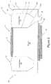
- FIG. 1illustrates certain embodiments of the present invention that provide a light emitting device 10 that is suitable for use as a single chip broad spectrum light emitting device and/or narrow band light conversion light emitting device.
- the light emitting device 10 illustrated in FIG. 1can provide broad spectrum light and/or converted narrow band light that may reduce the need to mount the device 10 on a submount or in a cup for holding light conversion material.
- a substrate 20such as a silicon carbide substrate, has a first contact 24 provided on a first surface 20 a of the substrate 20 and a light emitting element 26 provided on a second surface 20 b of the substrate 20 .
- a second contact 28may also be provided on the light emitting element 26 .
- the light emitting element 26may be any suitable semiconductor light emitting element that provides a narrow spectrum light that is broadened to provide broad spectrum light and/or shifted to provide a converted spectrum light.
- the light emitting element 26is a silicon carbide or gallium nitride based light emitting element.
- the light emitting element 26may be gallium nitride based LEDs or lasers fabricated on a silicon carbide substrate such as those devices manufactured and sold by Cree, Inc. of Durham, N.C.
- the present inventionmay be suitable for use with LEDs and/or lasers as described in U.S. Pat. Nos.
- the LEDs and/or lasersmay be configured to operate in a “flip-chip” configuration such that light emission occurs through the substrate.
- the substratemay be patterned so as to enhance light output of the devices as is described, for example, in U.S. Provisional Patent Application Ser. No. 60/307,235 filed Jul. 23, 2001 entitled “LIGHT EMITTING DIODES INCLUDING SUBSTRATE MODIFICATIONS FOR LIGHT EXTRACTION AND MANUFACTURING METHODS THEREFOR” or as described in U.S. patent application Ser. No. 10/057,821, filed Jan.
- the first and second contacts 24 and 28may be a suitable contact material based on the substrate material and the light emitting element material(s). Such contact materials are known to those of skill in the art and will not be described further herein. Furthermore, the first contact 24 and/or the second contact 28 may include a reflective layer (not separately shown) such as described in U.S. patent application Ser. No. 10/368,063, entitled “REFLECTIVE OHMIC CONTACTS FOR SILICON CARBIDE INCLUDING A LAYER CONSISTING OF NICKEL, METHODS OF FABRICATING SAME, AND LIGHT EMITTING DIODES INCLUDING THE SAME”, filed Feb. 14, 2003, the disclosure of which is incorporated herein by reference as if set forth fully herein.
- a trench 22is provided in the substrate 20 adjacent at least a portion of the periphery of the light emitting element 26 .
- the trench 22circumscribes the light emitting element 26 .
- the trench 22opens on the first surface 20 a of the substrate 20 opposite the light emitting element 26 .
- the trenchmay open on the second surface 20 b of the substrate 20 that is on the same side of the substrate 20 as the light emitting element 26 .
- the trench 22may be non-overlapping, partially overlapping or completely overlapping with the light emitting element 26 .
- the trench 22may be a complete or partial rectangle, square, circle, polygon, ellipses, and/or other such geometric configuration at least partially surrounding the light emitting element 26 .
- the trench 22may have a geometric shape that corresponds to the geometric shape of the light emitting element 26 .
- the trench 22is shaped so as to provide for light extraction from the substrate 20 .
- the sidewalls of the trench 22may be shaped to provide the substrate configurations described in the commonly assigned United States Patent Applications discussed herein.
- the trench 22has two tapered sidewalls 22 a and 22 b and a floor 22 c .
- the tapered sidewalls 22 a and 22 bextend from the floor 22 c to the first surface 20 a of the substrate 20 .
- the sidewall 22 aprovides a continuously tapered sidewall of the substrate 20 through which light from the light emitting element 26 is extracted.
- the sidewall 22 bmay be continuously tapered such that light from the sidewall 22 a that is incident on the sidewall 22 b is reflected back into the trench 22 and/or out the opening of the trench 22 .
- the sidewalls of the trench 22may be configured to provide light containment and/or diffusion.
- the light emitting device 10 illustrated in FIG. 1is defined by outer sidewalls 32 that extend through the substrate 20 so as to provide individual devices.
- Such devicesmay include one or more light emitting elements 26 as described, for example, commonly assigned in U.S. patent application Ser. No. 10/058,369, entitled “CLUSTER PACKAGING OF LIGHT EMITTING DIODES”, filed Jan. 28, 2002, the disclosure of which is incorporated herein by reference as if set forth fully herein.
- Singulation of individual devices from a wafer having a plurality of devicesmay, for example, be provided by sawing through the substrate 20 outside the trench 22 . Singulation could also be provided utilizing a combination of sawing, trench formation and breaking as described in commonly assigned U.S. patent application Ser. No.
- the light conversion material 30may, for example, be a luminous material.
- the luminous materialmay, for example, include phosphors such as YAG:Ce or the like and, in some embodiments, may include other materials for diffusion of light.
- phosphorssuch as YAG:Ce or the like and, in some embodiments, may include other materials for diffusion of light.
- CdSe Nanocrystals or similar materialthat are spherical II-VI, III-V, or IV-VI semiconductor crystals that are small enough such that quantum confinement effects predominate. In this size range, the physical size of the nanocrystals affects the optical and electronic properties they exhibit.
- the onset of absorption and the fluorescence wavelengthmay, thereby, be controlled.
- Currently available nanocrystalsinclude CdSe nanocrystals with or without a ZnS shell that have a tunable emission from 470-670 nm, and PbSe nanocrystals that have a tunable emission from 1000-2000 nm.
- the light conversion materialmay also be incorporated with other materials, for example, to provide a protective coating, to provide a coating that secures the light conversion material to the substrate, to provide a light conversion material with desired thermal properties or to provide a coating with suitable application properties, such as viscosity or drying time.
- the light conversion material 30which may be a luminous material, may be provided by, for example, a spin-on process or other blanket coating techniques, an inkjet application system, an air brush application system, a fluid application system, a dust application system utilizing charged particles which are attracted to light emitting elements having an opposite charge (electrostatic deposition), electrophoretic deposition, screen printing, dipping, roll coating and/or vacuum deposition and/or other suitable techniques known to those of skill in the art.
- the application of luminous materialmay be provided before or after singulation of the devices. Furthermore, application of the luminous material may occur before or after a device or devices are mounted to a submount if such mounting is utilized.
- Application of the light conversion material 30may be provided in a single application or in multiple applications, for example, in a layering process where different composition light conversion materials are provided at different depths in the trench 22 .
- Techniques for the application of luminous materialare described in U.S. Provisional Patent Application Ser. No. 60/335,649, filed Oct. 31, 2001, entitled “BROAD SPECTRUM LIGHT EMITTING DEVICES AND METHODS AND SYSTEMS FOR FABRICATING THE SAME,” and in U.S. patent application Ser. No. 10/267,093 filed Oct. 4, 2002 entitled “BROAD SPECTRUM LIGHT EMITTING DEVICES AND METHODS AND SYSTEMS FOR FABRICATING THE SAME,” the disclosures of which are incorporated herein by reference as if set forth fully herein.
- a reflective layer or coatingsuch as a layer of nickel or other reflective material, may be provided on the outer sidewall 22 b of the trench 22 .
- a reflective layer or coatingcould be provided on the sidewall 20 c of the substrate 20 .
- Such reflective layers or coatingsmay provide improved light conversion by reflecting light back into the light conversion material 30 .
- FIG. 2illustrates further embodiments of the present invention that provide a light emitting device 110 that is suitable for use as a single chip broad spectrum light emitting device.
- a substrate 120such as a silicon carbide substrate, has a first contact 124 provided on a first surface 120 a of the substrate 120 and a light emitting element 126 provided on a second surface 120 b of the substrate 120 .
- a second contact 128may also be provided on the light emitting element 126 .
- the light emitting element 126may be any suitable semiconductor light emitting element as described above with reference to the light emitting element 26 of FIG. 1 .
- the first and second contacts 124 and 128may be a suitable contact material based on the substrate material and the light emitting element material(s) as described above with reference to the contacts 24 and 28 of FIG. 1 .
- a trench 122is provided in the substrate 120 about at least a portion of the periphery of the light emitting element 126 .
- the trench 122circumscribes the light emitting element 126 .
- the trench 122opens on the first surface 120 a of the substrate 120 opposite the light emitting element 126 .
- the trench 122may be non-overlapping, partially overlapping or completely overlapping with the light emitting element 126 and may have a plan view configuration as described above with reference to the trench 22 .
- the trench 122is shaped so as to provide for light extraction from the substrate 120 . In the embodiments illustrated in FIG.
- the trench 122has two tapered sidewalls 122 a and 122 b , two non-tapered sidewalls 122 d and 122 e and a floor 122 c .
- the tapered sidewalls 122 a and 122 bextend from the floor 122 c to respective ones of the non-tapered sidewalls 122 d and 122 e .
- the non-tapered sidewalls 122 d and 122 eextend from the tapered sidewalls 122 a and 122 b to the first surface 120 a of the substrate 120 .
- the sidewall 22 aprovides a continuously tapered sidewall portion and a portion substantially perpendicular to the surface 120 a of the substrate 120 through which light from the light emitting element 126 is extracted.
- the sidewalls 122 b and 122 cmay be shaped such that light from the sidewalls 122 a and 122 d that is incident on the sidewalls 122 b and 122 e is reflected back into the trench 122 .
- the sidewalls of the trench 122may be configured to provide light containment.
- the light emitting device 110 illustrated in FIG. 2is defined by outer sidewalls 132 that extend through the substrate 120 so as to provide individual devices. Such devices may include one or more light emitting elements 26 as described above with reference to FIG. 1 . Furthermore, singulation may also be carried out as described about with reference to FIG. 1 .
- the trench 122contains a light conversion material 130 that may also include a light diffusion material as described above with reference to FIG. 1 .
- the light conversion material 130may completely fill or partially fill the trench 122 .
- the exposed surface 130 a of the light conversion material 130may be convex, concave or substantially parallel with respect to the first surface 120 a of the substrate 120 .
- the particular shape of the surface 130 a of the light conversion material 130may be selected so as to provide dispersion or concentration of light emitted from the light conversion material 130 .
- a reflective layer or coatingsuch as a layer of nickel or other reflective material, may be provided on the outer sidewall 122 b of the trench 122 .
- a reflective layer or coatingcould be provided on the sidewall 120 c of the substrate 120 .
- Such reflective layers or coatingsmay provide improved light conversion by reflecting light back into the light conversion material 130 .
- FIG. 3illustrates further embodiments of a light emitting device 10 ′ according to the present invention where both contacts of the device 10 ′ are on the same side of the substrate 20 .
- a first contact 40is provided on the surface 20 b of the substrate 20 .
- the first contact 40 and the second contact 28are both on the same side of the substrate 20 .
- Such a configurationmay facilitate “flip-chip” mounting of the device 10 ′.
- the light conversion material 30 ′is provided within the trench 22 and on at least a portion of the surface 20 a of the substrate 20 .
- the light conversion material 30 ′may also include a diffuser as discussed above with respect to the light conversion material 30 .
- the light conversion material 30 ′may be provided so that the exposed surface of the light conversion material forms a convex surface as illustrated in FIG. 3 .
- the light conversion material 30 ′may be provided as illustrated in FIG. 1 to completely cover the portion of the surface 20 a defined by the trench 22 or as covering less than all of the portion the surface 20 a .
- the reflective layers/coatingsmay also be provided on the sidewalls of the substrate and/or trench as described above with reference to FIGS. 1 and 2 .
- the trenches 22 and 122 illustrated in FIGS. 1 , 2 and 3may extend into the substrate 20 or 120 a predefined distance.
- the trenches 22 and 122may have a depth of about 120 ⁇ m for a 135 ⁇ m thick device or about 235 ⁇ m for a 250 ⁇ m thick device. Such thickness will, however, be dependent on the substrate thickness.
- the depth of the trenches 22 and 122may be such that at least about 15-25 ⁇ m of the substrate 20 or 120 remains.
- the width of the trenches 22 and 122may be about twice the depth of the trench multiplied by the tangent of 30° at their widest point and from about 20 ⁇ m to about 0 ⁇ m at their narrowest point. Each of these dimensions may vary depending on the amount of light conversion material 30 and 130 desired for a particular device.
- the shape of the trench 22 , 122may be selected so as to provide differing concentrations of the light conversion material based on the output of the light source so as to provide uniformity of conversion.
- more light conversion materialmay be provided closer to the light extraction surface 20 a and 120 a of the substrate 20 and 120 a so that additional light conversion material is provided where the light output of the device is increased.
- the slope or angle of the tapered sidewalls 22 a , 22 b , 122 a and 122 b with respect to the first surface 20 a and 120 amay be from about 60 to about 0 degrees.
- the length of the tapered portions 122 a and/or 122 bmay be from about 0 to about 100 percent of the total depth of the trench 122 .
- trenches described hereinhave been described with tapering sidewalls, straight sidewalls and/or a flat floor, other shapes may also be utilized.
- a curved flooreither convex or concave, and/or no floor could also be provided.
- a retrograde shape or curved shapemay be provided for one or more of the sidewalls.
- embodiments of the present inventionshould not be construed as limited to a particular shape trench but may include any shape of trench that may provide a moat for containing the light conversion material.
- holes or pitssuch as frusto-conical opening having slope sidewalls, a hole having straight sidewalls, holes having combinations of straight and slope sidewalls or the like, within the substrate 20 may be provided in a region proximate the light emitting element 26 and light conversion material provided within the holes or pits.
- An array of such openings with the array having uniformly spaced, non-uniformly spaced, regularly spaced and/or irregularly spaced openings, or a single openingcould be provided in the region of the light emitting element. Accordingly, embodiments of the present invention should not be construed as limited to a single trench or multiple trenches but may include any cavity configuration in the substrate 20 having opposing sidewalls capable of containing light conversion material.
- Embodiments of the present inventionmay be fabricated generally as described above.
- a lift-off techniquemay be utilized as illustrated in FIG. 4 .
- a photoresist layer 300may be provided on at least a portion of the region of substrate 20 between the trenches 22 .
- the photoresist 300may be provided on the contact 24 and/or a bond pad provided on the contact 24 and/or mirror structure if provided.
- the light conversion material 30may then be deposited, for example, by a spin-on process as described above.
- the photoresist 300may be removed before or after singulation of the device 10 .
- the photoresist 300may be utilized to give temporary height to the stricture during application of the light conversion material 30 and may also serve to maintain the integrity of the contact 24 and/or bond pad.
- the photoresist 300could be provided directly on the substrate 20 prior to formation of the contact 24 and removed for formation of the contact 24 .
- FIG. 5illustrates further embodiments of the present invention that provide a light emitting device 210 that is suitable for use as a single chip broad spectrum light emitting device.
- a substrate 220such as a silicon carbide substrate, has a first contact 224 provided on a first surface 220 a of the substrate 220 and a light emitting element 226 provided on a second surface 220 b of the substrate 220 .
- a second contact 228may also be provided on the light emitting element 226 .
- the light emitting element 226may be any suitable semiconductor light emitting element as described above with reference to the light emitting element 26 of FIG. 1 .
- the first and second contacts 224 and 228may be a suitable contact material based on the substrate material and the light emitting element material(s) as described above with reference to the contacts 24 and 28 of FIG. 1 .
- a trench 222is provided in the substrate 220 about at least a portion of the periphery of the light emitting element 226 .
- the trench 222circumscribes the light emitting element 226 .
- the trench 222opens on the first surface 220 a of the substrate 220 opposite the light emitting element 226 .
- the trench 222may be non-overlapping, partially overlapping or completely overlapping with the light emitting element 226 and may have a plan view configuration as described above with reference to the trench 22 .
- the trench 222is shaped so as to provide for light extraction from the substrate 220 . In the embodiments illustrated in FIG.
- the light emitting device 210 illustrated in FIG. 5is defined by outer sidewalls 232 that extend through the substrate 220 so as to provide individual devices. Such devices may include one or more light emitting elements 26 as described above with reference to FIG. 1 . Furthermore, singulation may also be carried out as described about with reference to FIG. 1 .
- the trench 222contains a light conversion material 230 that may also include a light diffusion material as described above with reference to FIG. 1 .
- the light conversion material 230may completely fill or partially fill the trench 222 .
- the exposed surface 230 a of the light conversion material 230may be convex, concave or substantially parallel with respect to the first surface 220 a of the substrate 220 .
- the particular shape of the surface 230 a of the light conversion material 230may be selected so as to provide dispersion or concentration of light emitted from the light conversion material 230 .
- a reflective layer or coating 240such as a layer of nickel or other reflective material, may be provided on the outer sidewall 222 b of the trench 222 .
- the reflective layer or coating 240could be provided on the sidewall 220 c of the substrate 220 .
- Such reflective layers or coatingsmay provide improved light conversion by reflecting light back into the light conversion material 230 .
- FIG. 6illustrates operations for formation of the trenches 22 and 122 and singulation of individual devices utilizing a sawing and/or sawing and breaking technique.
- a wafer 50may be sawn to a partial depth where the profile of the saw blade provides the profile of the trench.
- the width of the trenchmay correspond to the kerf of the saw blade and the depth of the trench may correspond to the cut depth of the saw blade.
- the partial depth saw cuts 52 that form the trench 22 , 122 of FIGS. 1-3are illustrated with broken lines in FIG. 6 .
- Subsequent complete saw cuts 54may then be provided to saw completely through the wafer 50 and singulate individual chips.
- differing depth saw cutsmay be made and the wafer 50 broken along the deeper saw cuts to provide singulation.
- a hub blade assembly that provides multiple cuts in a single passmay be particularly well suited for providing the multiple trenches/cuts illustrated in FIG. 6 .
- Other techniques for forming the trenches and/or singulation as described abovemay also be utilized.
- light emitting devices according to the present inventionmay be utilized with such structures.
- light emitting devices according to certain embodiments of the present inventionmay be encapsulated in a protective structure such as is conventionally done with existing light emitting devices and is described in the patents and/or patent application discussed herein.
- contact leadsmay be provided to the contacts/bond pads of the light emitting devices so as to facilitate use of the devices in an electrical circuit.
- light emitting devicesmay be mounted directly on a circuit board or substrate in a “chip-on-board” configuration with or without further encapsulation of the device.
Landscapes
- Led Device Packages (AREA)
Abstract
Description
Claims (26)
Priority Applications (2)
| Application Number | Priority Date | Filing Date | Title |
|---|---|---|---|
| US11/011,545US7405094B2 (en) | 2003-03-10 | 2004-12-14 | Light emitting devices for light conversion and methods and semiconductor chips for fabricating the same |
| US12/173,393US8941125B2 (en) | 2003-03-10 | 2008-07-15 | Light emitting devices for light conversion and semiconductor chips for fabricating the same |
Applications Claiming Priority (2)
| Application Number | Priority Date | Filing Date | Title |
|---|---|---|---|
| US10/385,034US6885033B2 (en) | 2003-03-10 | 2003-03-10 | Light emitting devices for light conversion and methods and semiconductor chips for fabricating the same |
| US11/011,545US7405094B2 (en) | 2003-03-10 | 2004-12-14 | Light emitting devices for light conversion and methods and semiconductor chips for fabricating the same |
Related Parent Applications (1)
| Application Number | Title | Priority Date | Filing Date |
|---|---|---|---|
| US10/385,034DivisionUS6885033B2 (en) | 2003-03-10 | 2003-03-10 | Light emitting devices for light conversion and methods and semiconductor chips for fabricating the same |
Related Child Applications (1)
| Application Number | Title | Priority Date | Filing Date |
|---|---|---|---|
| US12/173,393ContinuationUS8941125B2 (en) | 2003-03-10 | 2008-07-15 | Light emitting devices for light conversion and semiconductor chips for fabricating the same |
Publications (2)
| Publication Number | Publication Date |
|---|---|
| US20050098787A1 US20050098787A1 (en) | 2005-05-12 |
| US7405094B2true US7405094B2 (en) | 2008-07-29 |
Family
ID=32961420
Family Applications (3)
| Application Number | Title | Priority Date | Filing Date |
|---|---|---|---|
| US10/385,034Expired - LifetimeUS6885033B2 (en) | 2003-03-10 | 2003-03-10 | Light emitting devices for light conversion and methods and semiconductor chips for fabricating the same |
| US11/011,545Expired - LifetimeUS7405094B2 (en) | 2003-03-10 | 2004-12-14 | Light emitting devices for light conversion and methods and semiconductor chips for fabricating the same |
| US12/173,393Expired - LifetimeUS8941125B2 (en) | 2003-03-10 | 2008-07-15 | Light emitting devices for light conversion and semiconductor chips for fabricating the same |
Family Applications Before (1)
| Application Number | Title | Priority Date | Filing Date |
|---|---|---|---|
| US10/385,034Expired - LifetimeUS6885033B2 (en) | 2003-03-10 | 2003-03-10 | Light emitting devices for light conversion and methods and semiconductor chips for fabricating the same |
Family Applications After (1)
| Application Number | Title | Priority Date | Filing Date |
|---|---|---|---|
| US12/173,393Expired - LifetimeUS8941125B2 (en) | 2003-03-10 | 2008-07-15 | Light emitting devices for light conversion and semiconductor chips for fabricating the same |
Country Status (1)
| Country | Link |
|---|---|
| US (3) | US6885033B2 (en) |
Cited By (3)
| Publication number | Priority date | Publication date | Assignee | Title |
|---|---|---|---|---|
| US20070159062A1 (en)* | 2006-01-12 | 2007-07-12 | Luminoso Photoelectric Technology Co. | Light-enhanced element |
| US20090129053A1 (en)* | 2006-01-12 | 2009-05-21 | Luminoso Photoelectric Technology Co. | Light-enhanced element |
| US8033692B2 (en) | 2006-05-23 | 2011-10-11 | Cree, Inc. | Lighting device |
Families Citing this family (48)
| Publication number | Priority date | Publication date | Assignee | Title |
|---|---|---|---|---|
| KR100499129B1 (en)* | 2002-09-02 | 2005-07-04 | 삼성전기주식회사 | Light emitting laser diode and fabricatin method thereof |
| US6885033B2 (en)* | 2003-03-10 | 2005-04-26 | Cree, Inc. | Light emitting devices for light conversion and methods and semiconductor chips for fabricating the same |
| DE10316769A1 (en)* | 2003-04-10 | 2004-10-28 | Patent-Treuhand-Gesellschaft für elektrische Glühlampen mbH | Luminescence conversion LED used in optical semiconductor components has LED chip emitting primary radiation in specified region which is partially or completely converted into longer wavelength radiation |
| US7202181B2 (en)* | 2004-03-26 | 2007-04-10 | Cres, Inc. | Etching of substrates of light emitting devices |
| JP2006086469A (en)* | 2004-09-17 | 2006-03-30 | Matsushita Electric Ind Co Ltd | Semiconductor light emitting device, illumination module, illumination device, and method for manufacturing semiconductor light emitting device |
| US20060097385A1 (en)* | 2004-10-25 | 2006-05-11 | Negley Gerald H | Solid metal block semiconductor light emitting device mounting substrates and packages including cavities and heat sinks, and methods of packaging same |
| JP2006156837A (en)* | 2004-11-30 | 2006-06-15 | Matsushita Electric Ind Co Ltd | Semiconductor light emitting device, light emitting module, and lighting device |
| WO2007103310A2 (en)* | 2006-03-07 | 2007-09-13 | Qd Vision, Inc. | An article including semiconductor nanocrystals |
| US8718437B2 (en) | 2006-03-07 | 2014-05-06 | Qd Vision, Inc. | Compositions, optical component, system including an optical component, devices, and other products |
| US20070012928A1 (en)* | 2005-07-13 | 2007-01-18 | Zouyan Peng | Light emitting diode comprising semiconductor nanocrystal complexes and powdered phosphors |
| EP1908126A4 (en)* | 2005-07-13 | 2010-08-18 | Evident Technologies Inc | SEMICONDUCTOR NANOCRYSTALLINE COMPLEX ELECTROLUMINESCENT DIODE |
| CN101248535B (en)* | 2005-08-24 | 2011-09-07 | 皇家飞利浦电子股份有限公司 | Light emitting diodes and lasers diodes with color converters |
| US7196354B1 (en) | 2005-09-29 | 2007-03-27 | Luminus Devices, Inc. | Wavelength-converting light-emitting devices |
| US7772604B2 (en) | 2006-01-05 | 2010-08-10 | Illumitex | Separate optical device for directing light from an LED |
| US9874674B2 (en) | 2006-03-07 | 2018-01-23 | Samsung Electronics Co., Ltd. | Compositions, optical component, system including an optical component, devices, and other products |
| US9951438B2 (en) | 2006-03-07 | 2018-04-24 | Samsung Electronics Co., Ltd. | Compositions, optical component, system including an optical component, devices, and other products |
| US20090275157A1 (en)* | 2006-10-02 | 2009-11-05 | Illumitex, Inc. | Optical device shaping |
| WO2008042351A2 (en) | 2006-10-02 | 2008-04-10 | Illumitex, Inc. | Led system and method |
| US20080121911A1 (en)* | 2006-11-28 | 2008-05-29 | Cree, Inc. | Optical preforms for solid state light emitting dice, and methods and systems for fabricating and assembling same |
| US8836212B2 (en) | 2007-01-11 | 2014-09-16 | Qd Vision, Inc. | Light emissive printed article printed with quantum dot ink |
| US7918596B2 (en)* | 2007-04-20 | 2011-04-05 | Federal Signal Corporation | Warning light |
| US20080283864A1 (en)* | 2007-05-16 | 2008-11-20 | Letoquin Ronan P | Single Crystal Phosphor Light Conversion Structures for Light Emitting Devices |
| WO2009014590A2 (en) | 2007-06-25 | 2009-01-29 | Qd Vision, Inc. | Compositions and methods including depositing nanomaterial |
| WO2009014707A2 (en) | 2007-07-23 | 2009-01-29 | Qd Vision, Inc. | Quantum dot light enhancement substrate and lighting device including same |
| US8128249B2 (en)* | 2007-08-28 | 2012-03-06 | Qd Vision, Inc. | Apparatus for selectively backlighting a material |
| US7717591B2 (en)* | 2007-12-27 | 2010-05-18 | Lumination Llc | Incorporating reflective layers into LED systems and/or components |
| US20090309114A1 (en)* | 2008-01-16 | 2009-12-17 | Luminus Devices, Inc. | Wavelength converting light-emitting devices and methods of making the same |
| JP2011512037A (en) | 2008-02-08 | 2011-04-14 | イルミテックス, インコーポレイテッド | System and method for emitter layer shaping |
| US8324723B2 (en)* | 2008-03-25 | 2012-12-04 | Bridge Semiconductor Corporation | Semiconductor chip assembly with bump/base heat spreader and dual-angle cavity in bump |
| US8314438B2 (en)* | 2008-03-25 | 2012-11-20 | Bridge Semiconductor Corporation | Semiconductor chip assembly with bump/base heat spreader and cavity in bump |
| US20110163348A1 (en)* | 2008-03-25 | 2011-07-07 | Bridge Semiconductor Corporation | Semiconductor chip assembly with bump/base heat spreader and inverted cavity in bump |
| US8354688B2 (en) | 2008-03-25 | 2013-01-15 | Bridge Semiconductor Corporation | Semiconductor chip assembly with bump/base/ledge heat spreader, dual adhesives and cavity in bump |
| US9207385B2 (en) | 2008-05-06 | 2015-12-08 | Qd Vision, Inc. | Lighting systems and devices including same |
| WO2009137053A1 (en) | 2008-05-06 | 2009-11-12 | Qd Vision, Inc. | Optical components, systems including an optical component, and devices |
| WO2009151515A1 (en) | 2008-05-06 | 2009-12-17 | Qd Vision, Inc. | Solid state lighting devices including quantum confined semiconductor nanoparticles |
| TW201034256A (en) | 2008-12-11 | 2010-09-16 | Illumitex Inc | Systems and methods for packaging light-emitting diode devices |
| US8585253B2 (en) | 2009-08-20 | 2013-11-19 | Illumitex, Inc. | System and method for color mixing lens array |
| US8449128B2 (en) | 2009-08-20 | 2013-05-28 | Illumitex, Inc. | System and method for a lens and phosphor layer |
| US9991427B2 (en)* | 2010-03-08 | 2018-06-05 | Cree, Inc. | Photonic crystal phosphor light conversion structures for light emitting devices |
| CN101916819A (en)* | 2010-07-29 | 2010-12-15 | 张汝京 | Light emitting diode and manufacturing method thereof |
| CN102130251B (en)* | 2010-09-28 | 2014-09-03 | 映瑞光电科技(上海)有限公司 | Light emitting diode (LED) and manufacturing method thereof |
| KR101726807B1 (en) | 2010-11-01 | 2017-04-14 | 삼성전자주식회사 | Light Emitting Device |
| DE102010051286A1 (en)* | 2010-11-12 | 2012-05-16 | Osram Opto Semiconductors Gmbh | Optoelectronic semiconductor chip and method for its production |
| GB201109065D0 (en)* | 2011-05-31 | 2011-07-13 | Nanoco Technologies Ltd | Semiconductor nanoparticle-containing materials and light emitting devices incorporating the same |
| US9929325B2 (en) | 2012-06-05 | 2018-03-27 | Samsung Electronics Co., Ltd. | Lighting device including quantum dots |
| DE102013105533A1 (en)* | 2013-05-29 | 2014-12-04 | Osram Opto Semiconductors Gmbh | Inorganic optical element and method for producing an inorganic optical element |
| US20150153622A1 (en)* | 2013-12-03 | 2015-06-04 | Sage Electrochromics, Inc. | Methods for producing lower electrical isolation in electrochromic films |
| TWI780936B (en)* | 2021-09-30 | 2022-10-11 | 友達光電股份有限公司 | Display device |
Citations (30)
| Publication number | Priority date | Publication date | Assignee | Title |
|---|---|---|---|---|
| US4918497A (en) | 1988-12-14 | 1990-04-17 | Cree Research, Inc. | Blue light emitting diode formed in silicon carbide |
| US4966862A (en) | 1989-08-28 | 1990-10-30 | Cree Research, Inc. | Method of production of light emitting diodes |
| US5027168A (en) | 1988-12-14 | 1991-06-25 | Cree Research, Inc. | Blue light emitting diode formed in silicon carbide |
| US5210051A (en) | 1990-03-27 | 1993-05-11 | Cree Research, Inc. | High efficiency light emitting diodes from bipolar gallium nitride |
| US5338944A (en) | 1993-09-22 | 1994-08-16 | Cree Research, Inc. | Blue light-emitting diode with degenerate junction structure |
| US5393993A (en) | 1993-12-13 | 1995-02-28 | Cree Research, Inc. | Buffer structure between silicon carbide and gallium nitride and resulting semiconductor devices |
| US5416342A (en) | 1993-06-23 | 1995-05-16 | Cree Research, Inc. | Blue light-emitting diode with high external quantum efficiency |
| US5523589A (en) | 1994-09-20 | 1996-06-04 | Cree Research, Inc. | Vertical geometry light emitting diode with group III nitride active layer and extended lifetime |
| US5604135A (en) | 1994-08-12 | 1997-02-18 | Cree Research, Inc. | Method of forming green light emitting diode in silicon carbide |
| US5631190A (en) | 1994-10-07 | 1997-05-20 | Cree Research, Inc. | Method for producing high efficiency light-emitting diodes and resulting diode structures |
| US5739554A (en) | 1995-05-08 | 1998-04-14 | Cree Research, Inc. | Double heterojunction light emitting diode with gallium nitride active layer |
| US5813753A (en)* | 1997-05-27 | 1998-09-29 | Philips Electronics North America Corporation | UV/blue led-phosphor device with efficient conversion of UV/blues light to visible light |
| JP2000347601A (en) | 1999-06-02 | 2000-12-15 | Toshiba Electronic Engineering Corp | Light emitting device |
| US6187606B1 (en) | 1997-10-07 | 2001-02-13 | Cree, Inc. | Group III nitride photonic devices on silicon carbide substrates with conductive buffer interlayer structure |
| US6245259B1 (en) | 1996-09-20 | 2001-06-12 | Osram Opto Semiconductors, Gmbh & Co. Ohg | Wavelength-converting casting composition and light-emitting semiconductor component |
| US20020123164A1 (en)* | 2001-02-01 | 2002-09-05 | Slater David B. | Light emitting diodes including modifications for light extraction and manufacturing methods therefor |
| GB2373368A (en) | 2001-03-12 | 2002-09-18 | Arima Optoelectronics Corp | White light emitting LED devices |
| US20030006418A1 (en) | 2001-05-30 | 2003-01-09 | Emerson David Todd | Group III nitride based light emitting diode structures with a quantum well and superlattice, group III nitride based quantum well structures and group III nitride based superlattice structures |
| US20030030060A1 (en) | 2001-08-07 | 2003-02-13 | Tadahiro Okazaki | White semiconductor light-emitting device |
| US20030038295A1 (en)* | 2001-08-22 | 2003-02-27 | Nichia Corporation | Light emitting device with fluorescent member excited by semiconductor light emitting element |
| US20030038291A1 (en) | 2001-08-24 | 2003-02-27 | Densen Cao | Semiconductor light source |
| US20030080341A1 (en) | 2001-01-24 | 2003-05-01 | Kensho Sakano | Light emitting diode, optical semiconductor element and epoxy resin composition suitable for optical semiconductor element and production methods therefor |
| US20030089918A1 (en) | 2001-10-31 | 2003-05-15 | Norbert Hiller | Broad spectrum light emitting devices and methods and systems for fabricating the same |
| JP2003224307A (en) | 2003-02-06 | 2003-08-08 | Nichia Chem Ind Ltd | Light emitting diode and method of forming the same |
| US20030168663A1 (en) | 2001-02-01 | 2003-09-11 | Slater David B. | Reflective ohmic contacts for silicon carbide including a layer consisting essentially of nickel, methods of fabricating same, and light emitting devices including the same |
| US6635503B2 (en)* | 2002-01-28 | 2003-10-21 | Cree, Inc. | Cluster packaging of light emitting diodes |
| US6638780B2 (en)* | 2001-06-12 | 2003-10-28 | Citizen Electronics Co., Ltd. | Method for manufacturing light emitting diode devices |
| US20040051118A1 (en) | 2002-07-19 | 2004-03-18 | Bruhns Michael T. | Trench cut light emitting diodes and methods of fabricating same |
| US20040056260A1 (en) | 2002-09-19 | 2004-03-25 | Slater David B. | Phosphor-coated light emitting diodes including tapered sidewalls, and fabrication methods therefor |
| US6841933B2 (en)* | 2001-06-15 | 2005-01-11 | Toyoda Gosei Co., Ltd. | Light-emitting device |
Family Cites Families (16)
| Publication number | Priority date | Publication date | Assignee | Title |
|---|---|---|---|---|
| US5923987A (en)* | 1997-06-30 | 1999-07-13 | Sun Microsystems, Inc. | Method for forming MOS devices with retrograde pocket regions and counter dopant regions at the substrate surface |
| US6329676B1 (en)* | 1999-03-01 | 2001-12-11 | Toru Takayama | Flat panel solid state light source |
| DE50113755D1 (en) | 2000-05-29 | 2008-04-30 | Patent Treuhand Ges Fuer Elektrische Gluehlampen Mbh | WHITE-EMITTING LIGHTING UNIT ON LED BASE |
| JP4386693B2 (en) | 2000-05-31 | 2009-12-16 | パナソニック株式会社 | LED lamp and lamp unit |
| US6577073B2 (en) | 2000-05-31 | 2003-06-10 | Matsushita Electric Industrial Co., Ltd. | Led lamp |
| KR100338778B1 (en)* | 2000-08-21 | 2002-05-31 | 윤종용 | Method for fabricating MOS transistor using selective silicide process |
| DE60137972D1 (en) | 2001-04-12 | 2009-04-23 | Matsushita Electric Works Ltd | LIGHT SOURCE ELEMENT WITH LED AND METHOD FOR THE PRODUCTION THEREOF |
| JP4822482B2 (en)* | 2001-05-23 | 2011-11-24 | シチズン電子株式会社 | Light emitting diode and manufacturing method thereof |
| TW482103U (en)* | 2001-06-28 | 2002-04-01 | Chung-Hu Shiau | Multi-layered cloth materiel with compressing elasticity |
| TW567619B (en) | 2001-08-09 | 2003-12-21 | Matsushita Electric Industrial Co Ltd | LED lighting apparatus and card-type LED light source |
| US6885033B2 (en)* | 2003-03-10 | 2005-04-26 | Cree, Inc. | Light emitting devices for light conversion and methods and semiconductor chips for fabricating the same |
| KR20040092512A (en) | 2003-04-24 | 2004-11-04 | (주)그래픽테크노재팬 | A semiconductor light emitting device with reflectors having a cooling function |
| JP4922555B2 (en) | 2004-09-24 | 2012-04-25 | スタンレー電気株式会社 | LED device |
| US7322732B2 (en) | 2004-12-23 | 2008-01-29 | Cree, Inc. | Light emitting diode arrays for direct backlighting of liquid crystal displays |
| US8125137B2 (en) | 2005-01-10 | 2012-02-28 | Cree, Inc. | Multi-chip light emitting device lamps for providing high-CRI warm white light and light fixtures including the same |
| TWI256737B (en) | 2005-05-19 | 2006-06-11 | Pi-Fu Yang | One-block light-emitting device and manufacturing method thereof |
- 2003
- 2003-03-10USUS10/385,034patent/US6885033B2/ennot_activeExpired - Lifetime
- 2004
- 2004-12-14USUS11/011,545patent/US7405094B2/ennot_activeExpired - Lifetime
- 2008
- 2008-07-15USUS12/173,393patent/US8941125B2/ennot_activeExpired - Lifetime
Patent Citations (33)
| Publication number | Priority date | Publication date | Assignee | Title |
|---|---|---|---|---|
| US4918497A (en) | 1988-12-14 | 1990-04-17 | Cree Research, Inc. | Blue light emitting diode formed in silicon carbide |
| US5027168A (en) | 1988-12-14 | 1991-06-25 | Cree Research, Inc. | Blue light emitting diode formed in silicon carbide |
| US4966862A (en) | 1989-08-28 | 1990-10-30 | Cree Research, Inc. | Method of production of light emitting diodes |
| US5210051A (en) | 1990-03-27 | 1993-05-11 | Cree Research, Inc. | High efficiency light emitting diodes from bipolar gallium nitride |
| US5416342A (en) | 1993-06-23 | 1995-05-16 | Cree Research, Inc. | Blue light-emitting diode with high external quantum efficiency |
| US5338944A (en) | 1993-09-22 | 1994-08-16 | Cree Research, Inc. | Blue light-emitting diode with degenerate junction structure |
| US5393993A (en) | 1993-12-13 | 1995-02-28 | Cree Research, Inc. | Buffer structure between silicon carbide and gallium nitride and resulting semiconductor devices |
| US5604135A (en) | 1994-08-12 | 1997-02-18 | Cree Research, Inc. | Method of forming green light emitting diode in silicon carbide |
| US5523589A (en) | 1994-09-20 | 1996-06-04 | Cree Research, Inc. | Vertical geometry light emitting diode with group III nitride active layer and extended lifetime |
| US5631190A (en) | 1994-10-07 | 1997-05-20 | Cree Research, Inc. | Method for producing high efficiency light-emitting diodes and resulting diode structures |
| US5912477A (en) | 1994-10-07 | 1999-06-15 | Cree Research, Inc. | High efficiency light emitting diodes |
| US5739554A (en) | 1995-05-08 | 1998-04-14 | Cree Research, Inc. | Double heterojunction light emitting diode with gallium nitride active layer |
| US6120600A (en) | 1995-05-08 | 2000-09-19 | Cree, Inc. | Double heterojunction light emitting diode with gallium nitride active layer |
| US6245259B1 (en) | 1996-09-20 | 2001-06-12 | Osram Opto Semiconductors, Gmbh & Co. Ohg | Wavelength-converting casting composition and light-emitting semiconductor component |
| US5813753A (en)* | 1997-05-27 | 1998-09-29 | Philips Electronics North America Corporation | UV/blue led-phosphor device with efficient conversion of UV/blues light to visible light |
| US6201262B1 (en) | 1997-10-07 | 2001-03-13 | Cree, Inc. | Group III nitride photonic devices on silicon carbide substrates with conductive buffer interlay structure |
| US6187606B1 (en) | 1997-10-07 | 2001-02-13 | Cree, Inc. | Group III nitride photonic devices on silicon carbide substrates with conductive buffer interlayer structure |
| JP2000347601A (en) | 1999-06-02 | 2000-12-15 | Toshiba Electronic Engineering Corp | Light emitting device |
| US20030080341A1 (en) | 2001-01-24 | 2003-05-01 | Kensho Sakano | Light emitting diode, optical semiconductor element and epoxy resin composition suitable for optical semiconductor element and production methods therefor |
| US20020123164A1 (en)* | 2001-02-01 | 2002-09-05 | Slater David B. | Light emitting diodes including modifications for light extraction and manufacturing methods therefor |
| US20030168663A1 (en) | 2001-02-01 | 2003-09-11 | Slater David B. | Reflective ohmic contacts for silicon carbide including a layer consisting essentially of nickel, methods of fabricating same, and light emitting devices including the same |
| GB2373368A (en) | 2001-03-12 | 2002-09-18 | Arima Optoelectronics Corp | White light emitting LED devices |
| US20030006418A1 (en) | 2001-05-30 | 2003-01-09 | Emerson David Todd | Group III nitride based light emitting diode structures with a quantum well and superlattice, group III nitride based quantum well structures and group III nitride based superlattice structures |
| US6638780B2 (en)* | 2001-06-12 | 2003-10-28 | Citizen Electronics Co., Ltd. | Method for manufacturing light emitting diode devices |
| US6841933B2 (en)* | 2001-06-15 | 2005-01-11 | Toyoda Gosei Co., Ltd. | Light-emitting device |
| US20030030060A1 (en) | 2001-08-07 | 2003-02-13 | Tadahiro Okazaki | White semiconductor light-emitting device |
| US20030038295A1 (en)* | 2001-08-22 | 2003-02-27 | Nichia Corporation | Light emitting device with fluorescent member excited by semiconductor light emitting element |
| US20030038291A1 (en) | 2001-08-24 | 2003-02-27 | Densen Cao | Semiconductor light source |
| US20030089918A1 (en) | 2001-10-31 | 2003-05-15 | Norbert Hiller | Broad spectrum light emitting devices and methods and systems for fabricating the same |
| US6635503B2 (en)* | 2002-01-28 | 2003-10-21 | Cree, Inc. | Cluster packaging of light emitting diodes |
| US20040051118A1 (en) | 2002-07-19 | 2004-03-18 | Bruhns Michael T. | Trench cut light emitting diodes and methods of fabricating same |
| US20040056260A1 (en) | 2002-09-19 | 2004-03-25 | Slater David B. | Phosphor-coated light emitting diodes including tapered sidewalls, and fabrication methods therefor |
| JP2003224307A (en) | 2003-02-06 | 2003-08-08 | Nichia Chem Ind Ltd | Light emitting diode and method of forming the same |
Non-Patent Citations (12)
| Title |
|---|
| Bruhns, Michael, U.S. Appl. No. 60/397,488, filed Jul. 19, 2002. |
| Bruhns, Michael, U.S. Appl. No. 60/415,898, filed Oct. 3, 2002. |
| Emerson, David, U.S. Appl. No. 10/140,796, filed May 7, 2002. |
| Emerson, David, U.S. Appl. No. 60/294,308, filed May 30, 2001. |
| Emerson, David, U.S. Appl. No. 60/294,378, filed May 30, 2001. |
| Emerson, David, U.S. Appl. No. 60/294,445, filed May 30, 2001. |
| Glass, Robert, U.S. Appl. No. 10/057,821, filed Jan. 25, 2002. |
| Glass, Robert, U.S. Appl. No. 60/307,235, filed Jul. 23, 2001. |
| Hiller, Norbert, U.S. Appl. No. 10/267,093, filed Oct. 4, 2002. |
| Hiller, Norbert, U.S. Appl. No. 60/335,649, filed Oct. 31, 2001. |
| Slater, David, U.S. Appl. No. 60/411,980, filed Sep. 19, 2002. |
| Slater, et al., U.S. Appl. No. 10/368,063, filed Feb. 14, 2003. |
Cited By (4)
| Publication number | Priority date | Publication date | Assignee | Title |
|---|---|---|---|---|
| US20070159062A1 (en)* | 2006-01-12 | 2007-07-12 | Luminoso Photoelectric Technology Co. | Light-enhanced element |
| US20090129053A1 (en)* | 2006-01-12 | 2009-05-21 | Luminoso Photoelectric Technology Co. | Light-enhanced element |
| US8033692B2 (en) | 2006-05-23 | 2011-10-11 | Cree, Inc. | Lighting device |
| US8529104B2 (en) | 2006-05-23 | 2013-09-10 | Cree, Inc. | Lighting device |
Also Published As
| Publication number | Publication date |
|---|---|
| US20050098787A1 (en) | 2005-05-12 |
| US8941125B2 (en) | 2015-01-27 |
| US20080272386A1 (en) | 2008-11-06 |
| US6885033B2 (en) | 2005-04-26 |
| US20040178417A1 (en) | 2004-09-16 |
Similar Documents
| Publication | Publication Date | Title |
|---|---|---|
| US7405094B2 (en) | Light emitting devices for light conversion and methods and semiconductor chips for fabricating the same | |
| KR101182041B1 (en) | Phosphor-coated light emitting diodes including tapered sidewalls, and fabrication methods therefor | |
| US7863635B2 (en) | Semiconductor light emitting devices with applied wavelength conversion materials | |
| KR100499129B1 (en) | Light emitting laser diode and fabricatin method thereof | |
| KR20110017467A (en) | Trench cut light emitting diodes and methods of fabricating same | |
| US20230261154A1 (en) | Light-emitting diode packages with selectively placed light-altering materials and related methods | |
| KR20150004246A (en) | Light emitting devices having shielded silicon substrates | |
| TWI854189B (en) | Optical arrangements in cover structures for light emitting diode packages and related methods | |
| US11367810B2 (en) | Light-altering particle arrangements for light-emitting devices | |
| CN108604623A (en) | Conversion element and with this conversion element transmitting radiation semiconductor devices | |
| JP7705054B2 (en) | Light source and light emitting module | |
| TWI875120B (en) | Light emitting device with light-altering material layer, and fabrication method utilizing sealing template | |
| US20230106479A1 (en) | Lumiphoric material arrangements for multiple-junction light-emitting diodes | |
| TW202413843A (en) | Solid state light emitting components with unitary lens structures | |
| HK1075326B (en) | Phosphor-coated light emitting diodes including tapered sidewalls, and fabrication methods therefor |
Legal Events
| Date | Code | Title | Description |
|---|---|---|---|
| STCF | Information on status: patent grant | Free format text:PATENTED CASE | |
| CC | Certificate of correction | ||
| CC | Certificate of correction | ||
| FPAY | Fee payment | Year of fee payment:4 | |
| FPAY | Fee payment | Year of fee payment:8 | |
| MAFP | Maintenance fee payment | Free format text:PAYMENT OF MAINTENANCE FEE, 12TH YEAR, LARGE ENTITY (ORIGINAL EVENT CODE: M1553); ENTITY STATUS OF PATENT OWNER: LARGE ENTITY Year of fee payment:12 | |
| AS | Assignment | Owner name:CREE, INC., NORTH CAROLINA Free format text:ASSIGNMENT OF ASSIGNORS INTEREST;ASSIGNOR:ANDREWS, PETER S.;REEL/FRAME:055774/0586 Effective date:20030305 | |
| AS | Assignment | Owner name:CREE LED, INC., CALIFORNIA Free format text:ASSIGNMENT OF ASSIGNORS INTEREST;ASSIGNOR:CREE, INC.;REEL/FRAME:056012/0200 Effective date:20210301 | |
| AS | Assignment | Owner name:CITIZENS BANK, N.A., MASSACHUSETTS Free format text:SECURITY INTEREST;ASSIGNORS:SMART MODULAR TECHNOLOGIES, INC.;SMART HIGH RELIABILITY SOLUTIONS, LLC;SMART EMBEDDED COMPUTING, INC.;AND OTHERS;REEL/FRAME:058983/0001 Effective date:20220207 | |
| AS | Assignment | Owner name:SMART MODULAR TECHNOLOGIES, INC., CALIFORNIA Free format text:RELEASE OF PATENT SECURITY INTEREST RECORDED AT R/F 058983/0001;ASSIGNOR:CITIZENS BANK, N.A.;REEL/FRAME:071725/0207 Effective date:20250624 Owner name:SMART EMBEDDED COMPUTING, INC., ARIZONA Free format text:RELEASE OF PATENT SECURITY INTEREST RECORDED AT R/F 058983/0001;ASSIGNOR:CITIZENS BANK, N.A.;REEL/FRAME:071725/0207 Effective date:20250624 Owner name:SMART HIGH RELIABILITY SOLUTIONS LLC, CALIFORNIA Free format text:RELEASE OF PATENT SECURITY INTEREST RECORDED AT R/F 058983/0001;ASSIGNOR:CITIZENS BANK, N.A.;REEL/FRAME:071725/0207 Effective date:20250624 Owner name:CREELED, INC., CALIFORNIA Free format text:RELEASE OF PATENT SECURITY INTEREST RECORDED AT R/F 058983/0001;ASSIGNOR:CITIZENS BANK, N.A.;REEL/FRAME:071725/0207 Effective date:20250624 | |
| AS | Assignment | Owner name:CREELED, INC., CALIFORNIA Free format text:CORRECTIVE ASSIGNMENT TO CORRECT THE NAME OF THE ASSIGNEE PREVIOUSLY RECORDED ON REEL 56012 FRAME 200. ASSIGNOR(S) HEREBY CONFIRMS THE ASSIGNMENT;ASSIGNOR:CREE, INC.;REEL/FRAME:071874/0001 Effective date:20210301 |