US7404117B2 - Component testing and recovery - Google Patents
Component testing and recoveryDownload PDFInfo
- Publication number
- US7404117B2 US7404117B2US11/258,484US25848405AUS7404117B2US 7404117 B2US7404117 B2US 7404117B2US 25848405 AUS25848405 AUS 25848405AUS 7404117 B2US7404117 B2US 7404117B2
- Authority
- US
- United States
- Prior art keywords
- device component
- memory
- electronic device
- circuits
- excess
- Prior art date
- Legal status (The legal status is an assumption and is not a legal conclusion. Google has not performed a legal analysis and makes no representation as to the accuracy of the status listed.)
- Expired - Fee Related
Links
Images


Classifications
- G—PHYSICS
- G11—INFORMATION STORAGE
- G11C—STATIC STORES
- G11C29/00—Checking stores for correct operation ; Subsequent repair; Testing stores during standby or offline operation
- G11C29/70—Masking faults in memories by using spares or by reconfiguring
- G11C29/78—Masking faults in memories by using spares or by reconfiguring using programmable devices
- G11C29/84—Masking faults in memories by using spares or by reconfiguring using programmable devices with improved access time or stability
- G11C29/846—Masking faults in memories by using spares or by reconfiguring using programmable devices with improved access time or stability by choosing redundant lines at an output stage
- G—PHYSICS
- G11—INFORMATION STORAGE
- G11C—STATIC STORES
- G11C2229/00—Indexing scheme relating to checking stores for correct operation, subsequent repair or testing stores during standby or offline operation
- G11C2229/70—Indexing scheme relating to G11C29/70, for implementation aspects of redundancy repair
- G11C2229/74—Time at which the repair is done
- G11C2229/743—After packaging
- G—PHYSICS
- G11—INFORMATION STORAGE
- G11C—STATIC STORES
- G11C2229/00—Indexing scheme relating to checking stores for correct operation, subsequent repair or testing stores during standby or offline operation
- G11C2229/70—Indexing scheme relating to G11C29/70, for implementation aspects of redundancy repair
- G11C2229/76—Storage technology used for the repair
- G11C2229/763—E-fuses, e.g. electric fuses or antifuses, floating gate transistors
- G—PHYSICS
- G11—INFORMATION STORAGE
- G11C—STATIC STORES
- G11C29/00—Checking stores for correct operation ; Subsequent repair; Testing stores during standby or offline operation
- G11C29/56—External testing equipment for static stores, e.g. automatic test equipment [ATE]; Interfaces therefor
- G—PHYSICS
- G11—INFORMATION STORAGE
- G11C—STATIC STORES
- G11C29/00—Checking stores for correct operation ; Subsequent repair; Testing stores during standby or offline operation
- G11C29/70—Masking faults in memories by using spares or by reconfiguring
- G11C29/76—Masking faults in memories by using spares or by reconfiguring using address translation or modifications
- G—PHYSICS
- G11—INFORMATION STORAGE
- G11C—STATIC STORES
- G11C29/00—Checking stores for correct operation ; Subsequent repair; Testing stores during standby or offline operation
- G11C29/70—Masking faults in memories by using spares or by reconfiguring
- G11C29/78—Masking faults in memories by using spares or by reconfiguring using programmable devices
- G11C29/80—Masking faults in memories by using spares or by reconfiguring using programmable devices with improved layout
- G11C29/81—Masking faults in memories by using spares or by reconfiguring using programmable devices with improved layout using a hierarchical redundancy scheme
Definitions
- the inventionis in the field of electronics and more specifically in the fields of integrated circuit testing and assembly.
- SoCsystem-on-chip
- SiPsingle system-in-package
- SiMsingle system-in-module
- PoPpackage-in-package
- a disadvantage of generating a single electronic device from a set of discrete componentsis that the failure rate of the entire device is the product of the failure rate of each of the components. Once discrete components are assembled into a single electronic device, any failure can result in the loss of the entire electronic device. Thus, if a memory component has a five percent failure rate, an electronic device having four of these memory components will have at least an 18 percent failure rate. This aggregated failure rate can be very expensive.
- circuitscan be tested at the wafer lever, before the wafer on which they are produced is cut. They may also be repaired using laser fuses or anti-fuse technology. These repairs involve the use of excess circuits within the same individual device component as replacements for defective circuits. However, these systems cannot detect failures related to the assembly process, and the inclusion of excess circuits within the same individual device component can be costly. There is, therefore, a need for improved systems and methods of testing and/or increasing the yield of multi-component devices.
- Various embodiments of the inventioninclude systems and methods for increasing the manufacturing yield of electronic devices including more than one device component.
- These electronic devicesare typically embodied in an electronic device package and may include, for example, system-in-package (SiP), system-on-chip (SoC), system-in-module (SiM) systems, or package-in-package (PoP) systems.
- Manufacturing yieldmay be increased by identifying defects within individual device components and, through various approaches, compensating for the identified defects.
- the locations of circuits including defectsare identified in a memory component, e.g., a component including memory cells, and these locations are stored using fuses included in the memory component. These fuses may later be read in order to configure other device components packaged along with the memory component, such that the defects are avoided or replaced.
- the locations of the identified circuits including defectsare stored elsewhere, such as in a database.
- the stored information regarding the location of defective circuitsis optionally used to substitute excess memory circuits for those memory circuits including defects.
- the excess memory circuitscan be external to the memory component including the circuits being replaced.
- the excess memory circuitsmay be in another device component included within the same electronic device package.
- a memory componentmay be used in an electronic device, even when the memory component itself does not have sufficient excess memory circuits to replace all those that are defective.
- the excess memoryor other types of excess circuitry, configured for use as a substitute, may be disposed within a variety of component device types, within the same electronic device.
- this excess memoryis included in a processor, an application specific integrated circuit (ASIC), another memory circuit, an interface, or the like.
- ASICapplication specific integrated circuit
- Various embodiments of the inventionfurther include an interface included in an electronic device and configured to facilitate testing of other device components within the electronic device and/or configured for communication between various device components within the electronic device package.
- some embodimentsinclude an interface configured to operate in a normal mode in which the interface is used for communication between an ASIC and a memory component, or between an ASIC and an external electrical connector, and a test mode in which the interface is used for testing the memory component.
- Either the ASIC or the interfaceoptionally includes the excess memory configured for replacing memory in the memory component found to be defective through the testing processes.
- the interfaceis included within the memory component.
- the interfaceis configured for testing and repair of an assembled electronic device using anti-fuse technology.
- a shared electrical connector electronically coupled to the interfaceis used to access a memory component.
- the shared electrical connectormay be used to access the memory component in one mode, and to access a different device component in another mode.
- this accessis used for testing and/or repair of the memory component.
- Various embodiments of the inventioninclude a system comprising a first device component including a plurality of circuits, a second device component including excess circuits configurable to replace one or more of the plurality of circuits of the first device component, electronic device packaging incorporating the first device component and the second device component, and an electrical connector configured to receive programming instructions, the programming instructions being responsive to test data generated through testing of the first device component and being configured for replacing the one or more of the plurality of circuits with the excess circuits, the test data including an identity of a defective circuit within the plurality of circuits.
- Various embodiments of the inventioninclude a method comprising using a testing device to generate test results configured to identify one or more circuits including defects, the one or more circuits being disposed within a first device component, storing the test results, incorporating the first device component in an electronic device following the generation of the test results, incorporating a second device component within the electronic device, the second device component including one or more substitute circuits, and configuring the electronic device to replace the one or more circuits identified as including defects with the one or more excess circuits using the test results.
- Various embodiments of the inventioninclude a method comprising using a testing device to generate first test results data configured to identify one or more circuits including defects, the one or more circuits being disposed within a first device component and the testing occurring prior to incorporation of the first device component within an electronic device, and storing the first test results data, the first test results data being configured for replacing some of the one or more circuits including defects with excess circuits, the excess circuits being disposed within a second device component configured for incorporation within the electronic device.
- Various embodiments of the inventioninclude a system comprising means for identifying one or more circuits including defects, the one or more circuits being disposed within a first device component, means for storing information identifying the one or more circuits including defects prior to incorporation of the first device, component into an electronic device, means for reading the information stored, following incorporating the first device component into the electronic device, and means for programming the electronic device in order to compensate for the defects using the information read.
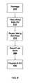
- FIG. 1illustrates an electronic device manufacturing system, according to various embodiments of the invention
- FIG. 2illustrates an electronic device, according to various embodiments of the invention
- FIG. 3illustrates methods of testing and/or repairing a circuit, according to various embodiments of the invention
- FIG. 4illustrates methods of compensating for defective circuits in an electronic device, according to various embodiments of the invention
- FIG. 5illustrates methods of compensating for defective circuits in an electronic device, according to various embodiments of the invention
- FIG. 6illustrates combined methods of compensating for defective circuits, according to various embodiments of the invention
- FIGS. 7A and 7Billustrate mappings of defective circuits to a fuse bank, according to various embodiments of the invention
- FIG. 8Aillustrates a memory tiling
- FIG. 8Billustrates mappings of defective circuits to a fuse bank, according to various alternative embodiments of the invention.
- Various embodiments of the inventioninclude systems for and methods of manufacturing an electronic device having a plurality of device components.
- the systems for manufacturingmay include, for example, device components, assembly systems, data systems, programming equipment and test equipment.
- the assembly systemsare configured for incorporating the device components into electronic device packaging to form the electronic device.
- the assembled electronic deviceincludes an excess of one or more circuit types.
- the device componentsinclude an excess of memory circuits.
- the excess of memory circuitsare used as replacements for any memory circuits determined to be defective using the test equipment.
- the excess memory circuitsare optionally disposed within a different device component than the defective circuits they are configurable to replace.
- the excess circuitsmay include logic circuits, sensors, data processing circuits, timing circuits, signal processing circuits, transducers, or the like.
- the assembled device componentsoptionally further include elements configured for storing data identifying which circuits are found to be defective.
- a memory componentincludes fuses configured for storing data identifying defective memory circuits within that memory component.
- Alternative embodimentsinclude a data system, external to the electronic device, configured for storing the data identifying which circuits are found to be defective.
- the stored informationis optionally used, after the device component has been incorporated in an electronic device, to reconfigure the electronic device such that the excess circuits are used to compensate for the defective circuits.
- the use of excess circuits, as substitutes for those found to be defective,advantageously increases the yield of the manufacturing process.
- Various embodiments of the inventioninclude the manufactured electronic device wherein excess circuitry in one device component has been used to replace circuitry, of another device component, found to be defective.
- the electronic devicecan include, for example, an application specific integrated circuit (ASIC), a microprocessor, a microcontroller, a digital signal processor (DSP), a field programmable gate array (FPGA), a programmable logic device (PLD), complex programmable logic device (CPLD), a sensor, an analog-to-digital converter, an analog signal processor, a digital signal processor and/or other electronic circuits.
- ASICapplication specific integrated circuit
- DSPdigital signal processor
- FPGAfield programmable gate array
- PLDprogrammable logic device
- CPLDcomplex programmable logic device
- the electronic devicecan further include memory, such as static random access memory (SRAM), dynamic random access memory (DRAM), synchronous DRAM (SDRAM), non-volatile random access memory (NVRAM), and read only memory (ROM), erasable programmable ROM (EPROM), electrically erasable programmable ROM (EEPROM), flash memory, or the like.
- SRAMstatic random access memory
- DRAMdynamic random access memory
- SDRAMsynchronous DRAM
- NVRAMnon-volatile random access memory
- ROMread only memory
- EPROMerasable programmable ROM
- EEPROMelectrically erasable programmable ROM
- flash memoryor the like.
- the excess circuitryis configurable for replacement of all or part of any of the above electronic device components.
- the electronic devicecan include various surface mount technologies such as a single in-line package (SIP), dual in-line package (DIP), zig-zag in-line package (ZIP), plastic leaded chip carrier (PLCC), small outline package (SOP), thin SOP (TSOP), flatpack, and quad flatpack (QFP), or the like.
- SIPsingle in-line package
- DIPdual in-line package
- ZIPzig-zag in-line package
- PLCCplastic leaded chip carrier
- SOPsmall outline package
- TSOPthin SOP
- flatpackflatpack
- QFPquad flatpack
- testing of the various electronic device componentsmay occur at a variety of times during the manufacturing (e.g., assembly) process. For example, in various embodiments, testing occurs at the wafer level prior to inclusion of a device component in the electronic device package, and then again after the device component is incorporated in the electronic device and the electronic device packaging is sealed such that internal components are only accessible through a limited set of electrical connectors that pass through the electronic device packaging.
- FIG. 1illustrates an Electronic Device Manufacturing System, generally designated 100 , according to various embodiments of the invention.
- Electronic Device Manufacturing System 100is configured to manufacture an electronic device including at least two device components, to test the manufactured electronic device, and to make use of excess circuits in one of the device components to replace circuits determined to be defective within another of the device components within the electronic device.
- Electronic Device Manufacturing System 100is optionally further configured to perform tests and/or repairs of circuits determined to be defective following assembly.
- some embodiments of Electronic Device Manufacturing System 100include test devices configured to test a device component through a multi-mode interface and to use anti-fuses to compensate for defects found during these tests.
- Electronic Device Manufacturing System 100includes an Assembly System 110 configured for assembling an Electronic Device 120 .
- the assembly of Electronic Device 120typically occurs in a series of assembly stages.
- these assembly stagescan be divided into a first stage (Stage 1 ) wherein a Device Component 130 is tested and optionally repaired, and a second stage (Stage 2 ) wherein the Device Component 130 is incorporated in Electronic Device 120 .
- Stage 1may include manufacture of a Device Component 130 at a first location
- Stage 2may include incorporation of the manufactured Device Component 130 in Electronic Device 120 after the Device Component 130 has been transported to a second location.
- Assembly System 110may be geographically distributed. Further details of the Assembly System 110 are discussed elsewhere herein.
- Electronic Device Manufacturing System 100further includes one or more Automated Testing Equipment/Programmer, referred to herein as ATE 140 , configured to test Device Component 130 at one or more assembly stages.
- Test data generated using ATE 140is optionally stored in a Database 150 for use in programming Electronic Device 120 in later stages of Assembly System 110 .
- the programming of Electronic Device 120can include configuring Electronic Device 120 to make use of excess circuits in order to replace or otherwise compensate for circuits within Device Component 130 that are found to be defective.
- Device Component 130may include, for example, an application specific integrated circuit (ASIC), a microprocessor, a microcontroller, a digital signal processor (DSP), a field programmable gate array (FPGA), programmable logic device (PLD), complex programmable logic device (CPLD), a sensor, an analog to digital converter, an analog signal processor, other circuit types discussed herein, and/or other circuitry.
- ASICapplication specific integrated circuit
- DSPdigital signal processor
- FPGAfield programmable gate array
- PLDprogrammable logic device
- CPLDcomplex programmable logic device
- sensoran analog to digital converter
- analog signal processorother circuit types discussed herein, and/or other circuitry.
- Device Component 130may further or alternatively include memory, such as, for example, static random access memory (SRAM), dynamic random access memory (DRAM), synchronous DRAM (SDRAM), non-volatile random access memory (NVRAM), and read only memory (ROM) such as erasable programmable ROM (EPROM) or electrically erasable programmable ROM (EEPROM), flash memory, or the like.
- SRAMstatic random access memory
- DRAMdynamic random access memory
- SDRAMsynchronous DRAM
- NVRAMnon-volatile random access memory
- ROMread only memory
- EPROMerasable programmable ROM
- EEPROMelectrically erasable programmable ROM
- Electronic Device 120includes one or more instances of Device Component 130 , typically within an electronic device package.
- Electronic Device 120may comprise, for example, system-in-package (SiP), system-on-chip (SoC), system-in-module (SiM) package-in-package (PoP) devices, or the like.
- the electronic device package of Electronic Device 120can include, for example, a single in-line package (SIP), dual in-line package (DIP), zig-zag in-line package (ZIP), plastic leaded chip carrier (PLCC), small outline package (SOP), thin SOP (TSOP), flatpack, and quad flatpack (QFP), or the like.
- SIPsingle in-line package
- DIPdual in-line package
- ZIPzig-zag in-line package
- PLCCplastic leaded chip carrier
- SOPsmall outline package
- TSOPthin SOP
- QFPquad flatpack
- Electronic Device 120is optionally an embodiment of Electronic Devices 10 , 50 or 900 as described in U.S. patent application Ser. No. 11/207,665, filed on Aug. 18, 2005, entitled “Electronic device having an interface supported testing mode,” or Circuit 90 as described in U.S. patent application Ser. No. 11/223,286, filed on Sep. 9, 2005, entitled “Shared Bond Pad for Testing a Memory within a Packaged Semiconductor Device.”
- Stage 1 of Assembly System 110is configured for manufacture, and optional testing of Device Component 130 .
- Stage 1may include a silicon foundry for manufacture of a memory circuit on a semiconductor die.
- An instance of ATE 140is optionally used to test and/or repair the manufactured device component.
- Stage 2 of Assembly System 110includes equipment for mounting one or more instances of Device Component 130 within an electronic device package and finishing the electronic device packaging of Electronic Device 120 .
- the apparatus included in Stage 2is optionally also configured to test and/or repair the one or more instances of Device Component 130 following the mounting process using an instance of ATE 140 .
- an instance of ATE 140 included in Stage 2is optionally configured for programming, (e.g., modifying or configuring), Electronic Device 120 such that any circuits found to be defective within Electronic Device 120 are replaced by excess circuitry within Electronic Device 120 .
- the excess circuitry used for replacement in Stage 2may be disposed within the tested instance of Device Component 130 or within another device component within Electronic Device 120 .
- FIG. 1illustrates instances Electronic Device 120 and Device Component 130 .
- the instance of Device Component 130 shownmay, at a later time be included in the instance of Electronic Device 120 .
- these instancesmay be representative of the same Electronic Device 120 or ATE 140 at different times during manufacturing, and/or representative of different instances of Electronic Device 120 or ATE 140 .
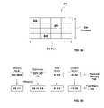
- FIG. 2illustrates further details of Electronic Device 120 , according to various embodiments of the invention.
- the instances of Electronic Device 120 illustrated in FIG. 2includes Memory 210 , an ASIC 220 and an Interface 230 .
- Memory 210 , ASIC 220 and Interface 230are configured to communicate through Communication Paths 233 , 235 and 237 , and are each illustrative embodiments of Device Component 130 .
- Interface 230is optionally included in Memory 210 or ASIC 220 .
- At least an Electrical Connector 240 and an Electrical Connector 250are configured for facilitating communication between Electronic Device 120 and electronics external to Electronic Device 120 .
- Electrical Connector 240 and Electrical Connector 250are typically pins, bond pads, or the like.
- Electrical Connector 240 and Electrical Connector 250typically extend through electronic device packaging of Electronic Device 120 .
- Electrical Connector 250is a shared electrical connector configured for communicating data to ASIC 220 in a normal operation mode and for communicating data to Memory 210 in a test mode or a programming mode.
- Electrical Connector 250is a shared electrical connector as discussed in U.S. patent application Ser. Nos. 11/223,286 and 11/207,665, referenced above.
- Interface 230is configured to convey signals between Memory 210 , ASIC 220 and Electrical Connector 250 , responsive to an operation mode, e.g., a normal operation mode, a test mode, a programming mode, or the like.
- Interface 230is configured for communicating signals between (e.g., to and from) Electrical Connector 250 and ASIC 220 in the normal operation mode and for communicating signals between Electrical Connector 250 and Memory 210 in the test mode.
- Interface 230is configured for communicating signals between ASIC 220 and Memory 210 in the normal operation mode and between Electrical Connector 250 and Memory 210 in the test mode.
- Interface 230is optionally configured to receive data serially in some modes and to receive part of a parallel data communication in other modes.
- Interface 230may include one or more buffers, or one or more multiplexers, configured for controlling how signals are communicated in various modes.
- Memory 210includes Memory Cells 270 , optional Excess Memory 280 and optional Data Storage 290 .
- Memory Cells 270are configured to store digital data received from ASIC 220 or Interface 230 .
- Excess Memory 280is memory configurable to replace defective memory circuits within Memory Cells 270 .
- Data Storage 290is configured to store information identifying the locations of defective memory circuits within Memory Cells 270 .
- Data Storage 290includes a series of fuses configured to encode the identity of locations within Memory Cells 270 .
- ASIC 220optionally includes a Memory Controller 260 configurable for mapping virtual memory addresses to physical memory.
- Memory Controller 260is initially configured to map virtual memory addresses to physical memory within Memory 210 (e.g., Memory Cells 270 ).
- ASIC 220optionally further includes Excess Memory 285 .
- Excess Memory 285includes memory cells configured to store digital data and to serve as substitutes for members of Memory Cells 270 that are found to be defective. Memory substitution using Excess Memory 285 can occur in Stage 2 of Assembly System 110 after Memory 210 is incorporated within Electronic Device 120 .
- Memory substitution using Excess Memory 285may occur at various granularities. For example, in some embodiments memory substitution occurs at the minimum granularity at which memory is addressed, e.g., byte, word, or the like. In various embodiments, memory substitution occurs on a single bit basis, a row basis, a column basis, a segment basis, an array basis, a sub-array basis, a memory bank basis, or the like. In alternative embodiments, Excess Memory 285 is located elsewhere within Electronic Device 120 . For example, Excess Memory 285 may be included in Interface 230 or some other Device Component 130 .
- Memory substitutionis optionally accomplished by altering a memory map within Memory Controller 260 .
- Memory Controller 260may include a memory map configured for converting virtual memory addresses to absolute (physical) memory addresses.
- Memory at a first physical location within Memory 210may be replaced by memory at a second physical location within Excess Memory 280 or Excess Memory 285 by exchanging their respective physical memory addresses within the memory map.
- memory substitutionis accomplished by burning fuses within Data Storage 290 . These fuses may be burned using laser light or electronic signals, or through other methods of fuse burning known in the art.
- Programming of Electronic Device 120 responsive to tests made using ATE 140may be accomplished according to several different approaches.
- programmingis performed using ATE 140 at approximately the same time that tests are performed.
- testing and programmingmay be part of the same operation.
- ATE 140may be placed in physical contact with Electronic Device 120 or Device Component 130 , and before this physical contact is broken both testing and programming are performed.
- programmingmay be performed sometime after testing.
- programming performed at assembly Stage 2may be performed responsive to tests performed in Stage 1 .
- tests resultsare optionally stored in Database 150 , ATE 140 or Data Storage 290 between the testing and programming procedures.
- data from tests performed at more than one assembly stagemay be aggregated and used in the same programming process. For example, tests performed using instances of ATE 140 at Stage 1 and Stage 2 may each generate results that are used for programming Electronic Device 120 in Stage 2 .
- the information regarding defective circuitsincludes data identifying a memory bank, a sub-array within the memory bank, and a column sector within the sub-array. In some embodiments, the information regarding defective circuits includes data identifying a memory bank, a sub-array within the memory bank, a row sector within the sub-array, and a column sector. Alternative representations are anticipated in alternative embodiments. In some embodiments, the granularity of the circuit replacement process is selected based on the probability of failure modes, e.g., single memory cells, single or double memory rows, single or double memory columns, etc. In these embodiments, the granularity of replacement is chosen to benefit assembly yield in view of available excess memory. Examples of how the information regarding defective circuits may be stored in Data Storage 190 are presented elsewhere herein.
- Interface 230is optionally configured to convey signals from Electrical Connector 250 to Memory 210 during programming of Electronic Device 120 .
- Interface 230is configured to convey signals from Electrical Connector 250 to Memory 210 for testing purposes and also programming purposes. Those signals conveyed for testing and programming purposes are optionally conveyed to different inputs of Memory 210 . Testing and programming can occur in ths same mode or in separate test and programming modes.
- Interface 230is configured to operate in three different modes: a normal operation mode, a testing mode, and a programming mode. In the programming mode, Interface 230 is configured to convey programming signals to one or more Device Component 130 within Electronic Device 120 in order to configure the use of excess circuits as replacement circuits.
- Excess Memory 270is included in Memory 210 , ASIC 220 , or another Device Component 130 within Electronic Device 120 .
- Excess Memory 270may be included in an instance of Device Component 130 distinct from Memory 210 and ASIC 220 .
- Memory Controller 260is included in Memory 210 , or some other part of Electronic Device 120 .
- FIG. 3illustrates methods of testing and/or repairing a Device Component 130 in Stage 1 of Assembly System 110 , according to various embodiments of the invention.
- tests of Memory Cells 170performed using ATE 140 . Results from these tests are optionally are used to program (e.g., reconfigure) Memory 210 such that all or part of Excess Memory 280 are used to replace defective members of Memory Cells 270 .
- Memory 210can be tested a second time to confirm that the replacement process was successful and/or to test Memory 210 under different conditions (e.g., at a different temperature). Tests results, generated from either testing, may be used to replace defective circuits within Memory Cells 270 with all or part of Excess Memory 280 .
- Test resultsindicate that the amount of Excess Memory 280 within Memory 210 is insufficient to replace the defective circuits, Electronic Device 120 is optionally discarded.
- the locations of un-replaced defective circuits within Memory Cells 270are stored in Data Storage 290 or Database 150 for later use.
- the steps illustrated in FIG. 3may be performed without moving Electronic Device 120 or disconnecting ATE 140 from Electronic Device 120 .
- a First Wafer Level Test Step 310Device Component 130 is tested using ATE 140 prior to inclusion within Electronic Device 120 (e.g., in Stage 1 of Assembly System 110 ).
- the tested Device Component 130may be rejected for incorporation within Electronic Device 120 if the number and/or types of defects discovered within Memory Cells 270 are above a certain predetermined level and excepted if the number of defects is equal to or below this predetermined level.
- the predetermined levelis optionally greater than the capacity of Excess Memory 280 to replace defective circuits within Memory Cells 270 .
- Memory 210is repaired by replacing defective circuits identified in First Wafer Level Test Step 310 with all or part of Excess Memory 280 .
- these repairsare made using laser based techniques.
- these repairsare made using anti-fuse technology.
- the number of defects within Memory Cells 270 that can be repaired in Repair at Wafer Level Step 320is limited by the number of replacement circuits available within Excess Memory 280 .
- a Store Results Step 330the identities of any members of Memory Cells 270 found to be defective in First Wafer Level Test Step 310 , but not replaced using Excess Memory 280 in Repair at Wafer Level Step 320 , are stored. This storage may occur in Database 150 and/or Data Storage 290 . In some embodiments, fuses are used to store the identities in Data Storage 290 . Methods of encoding the identities of members of Memory Cells 270 using fuses are described elsewhere herein. In some embodiments, the stored information is configured to identify memory, e.g., cells, bytes, words, rows, columns, segments, banks, etc., within Memory 210 that include one or more defective memory cells.
- Database 150When the identities are stored in Database 150 , they are stored in association with the particular instance of Memory 210 tested such that they can be retrieved after that instance of Memory 210 is incorporated in Electronic Device 120 .
- Database 150is optionally configured to store test results for a plurality of Devices Components 130 .
- Second Wafer Level Test Step 340Memory 210 is tested using ATE 140 . These tests are similar to those of First Wafer Level Test Step 310 . However, Second Wafer Level Test Step 340 may be performed under different circumstances, for example at a different temperature. Further, in Second Wafer Level Test Step 340 those circuits within Memory Cells 270 previously identified as being defective need not be tested again. Following Second Wafer Level Test Step 340 , if it is determined that the number of defects within Memory Cells 270 is greater than may be replaced using Excess Memory 280 and Excess Memory 285 , then the tested instance of Memory 210 may be discarded.
- any members of Memory Cells 270 found to be defective in Second Wafer Level Test Step 340are replaced using Excess Memory 280 .
- the replacement processmay be similar to that discussed above with respect to Repair at Wafer Level Step 320 .
- Store Results Step 360the identities of any members of Memory Cells 270 found to be defective in Second Wafer Level Test 340 and not repaired in Repair at Wafer Level Step 350 are stored. Storage may occur in Database 150 and/or Data Storage 290 . The identities stored in Store Results Step 330 and Store Results Step 360 are configured to be used to replace members of Memory Cells 270 using excess memory external to Memory 210 , e.g., Excess Memory 285 .
- FIG. 4illustrates methods of compensating for defective circuits in Electronic Device 120 in Stage 2 of Assembly system 110 .
- the instance of Device Component 130 tested in the methods illustrated by FIG. 3is incorporated within an instance of Electronic Device 120 .
- the identities of defective circuits stored in Store Results Step 230 or 260are read and used to reconfigure the instance of Electronic Device 120 to compensate for these defects.
- Electronic Device 120may be programmed to use Excess Memory 285 as a substitute for defective members of Memory Cells 270 .
- Memory 210is incorporated within Electronic Device 120 .
- incorporationincludes mounting of Device Component 130 within a packaging of Electronic Device 120 and/or establishment of electrical connections between electrical connectors of Device Component 130 and electrical connectors of Electronic Device 120 (e.g., Electrical Connectors 240 or 250 ).
- Electronic Device 120also includes further instances of Device Component 130 , for example, as illustrated in FIG. 2 . These further instances are optionally also incorporated within Electronic Device 120 in Package Step 410 .
- Package Step 410typically includes finishing (e.g., closing) of the packaging of Electronic Device 120 .
- a Read Fuse Bank Step 420the identities of any defective circuits within Memory Cells 270 , that are not already replaced using Excess Memory 280 , are read from Data Storage 290 or Database 150 . In some embodiments, this information is read from Data Storage 290 through Interface 230 and shared Electrical Connector 250 . In these embodiments, Interface 230 is placed in a read/test mode by sending an appropriate signal to Interface 230 . In the read/test mode, Interface 230 is configured to convey signals from Electrical Connector 250 to Memory 210 rather than from Electrical Connector 250 to ASIC 220 . Further details of switching Electronic Device 120 to read/test mode (e.g., test mode), according to some embodiments, are discussed in U.S. patent application Ser. Nos. 11/207,665 and 11/223,286. The identities are optionally read using an instance of ATE 140 .
- a Program ASIC Step 430the identities read in Read Fuse Bank Step 420 are used to program (e.g., configure) Electronic Device 120 such that Excess Memory 285 is used as replacements for circuits within Memory Cells 270 found to be defective.
- Programmingmay include configuration of Memory Controller 260 , burning of fuses, or the like.
- programmingis performed using an instance of ATE 140 . Instances of ATE 140 configured for reading Data Storage 290 and/or programming ASIC 220 are optionally not configured for testing Memory 210 or Electronic Device 120 or vice versa.
- FIG. 5illustrates methods of compensating for defective circuits in an electronic device, such as Electronic Device 120 , in Stage 2 of Assembly System 110 .
- the electronic deviceis tested using ATE 140 via shared Electrical Connector 250 and Interface 230 .
- this testingmay be used to confirm the success of repairs made in Repair at Wafer Level Step 350 and/or to detect defects resulting from packaging of Device Component 130 in Electronic Device 120 .
- Test Step 510typically occurs when Memory 210 is no longer directly accessible to ATE 140 .
- testingis performed via Electrical Connector 240 , Electrical Connector 250 and/or other electrical connectors disposed to convey signals between device components within Electronic Device 120 and systems external to Electronic Device 120 .
- the testing of Memory 210 using shared Electrical Connector 250 and Interface 230is further described in U.S. patent application Ser. No. 11/207,665, filed on Aug. 18, 2005, entitled “Electronic device having an interface supported testing mode,” or Circuit 90 as described in U.S. patent application Ser. No. 11/223,286, filed on Sep. 9, 2005, entitled “Shared Bond Pad for Testing a Memory within a Packaged Semiconductor Device.”
- any defects within Memory 210 identified in Test Step 510are repaired using anti-fuse technology. These repairs are optionally made using ATE 140 .
- Communication between Memory 210 and ATE 140is passed through Interface 230 and shared Electrical Connector 250 .
- Interface 230is first placed in a program mode similar to the test/program mode (e.g., test mode) discussed in U.S. patent application Ser. Nos. 11/207,665 and 11/223,286.
- Repair Using Anti-fuse Step 520includes programming of Memory Controller 260 using commands sent to ASIC 220 rather than the use of anti-fuse technology within Memory 210 . Repair Using Anti-Fuse Step 520 may only be possible when there is available Excess Memory 280 .
- FIG. 6illustrates combined methods of compensating for defective circuits. These methods include combinations of steps illustrated in FIGS. 4 and 5 . These steps may be performed in a variety of orders. For example, in contrast with FIG. 6 , Steps 420 and/or 430 may be performed prior to Steps 510 and 520 .
- FIGS. 7A and 7Billustrate approaches to mapping defective circuits within Memory 210 to Data Storage 290 , in embodiments where Data Storage 290 includes a Fuse Bank 710 .
- FIGS. 7A and 7Bdiffer in the granularity of the circuits identified.
- DRAMdynamic random access memory
- F 4 and F 3are used to identify a specific memory bank within Physical Memory 720 of Memory Cells 270
- three fusesare used to identify a specific Sub-Array within the identified memory bank.
- DRAMdynamic random access memory
- Each sub-array segmentis optionally decoded by row addresses A 11 , A 10 , and A 9 .
- Each of these row addressesaddresses 8 sub-array blocks in a bank or sub bank depending on the memory density.
- a total of 512 rowsmay be included within a sub-array segment. These rows are identified using row addresses A 8 -A 0 .
- Fuse Bank 710includes five fuses F 6 -F 0 . These fuses are optionally based on DRAM laser fuse technology. To identify bank 2 , sub-array 5 as a sector including defects, a laser fuse bit pattern of 10101 may be used, where a blown fuse indicates a logical “0.”
- FIG. 7Billustrates a mapping of Physical Memory 720 to an embodiment of Fuse Bank 710 having greater granularity than the embodiments illustrated in FIG. 7A .
- 7 fusesare used and a partial row may be identified.
- This mappingis configurable, for example, to identify 64 columns (1 ⁇ 4 of 256 columns) on a 512-row sub-array (assuming a 256-column address configuration and a 512 row per sub-array segment architecture).
- FIGS. 8A and 8Billustrate alternative embodiments of identifying members of Memory Cells 270 including defects using Fuse Bank 710 included in Data Storage 290 .
- the illustrated approachesare based on a tile structure within a memory bank.
- FIG. 8Aillustrates a 512-row by 256-column Sub-array Segment, generally designated 810 , divided into 16 Tiles 820 each including 128 rows by 64 columns.
- Alternative, embodiments of Tiles 820may include different numbers of rows and columns. For example, one embodiment includes 4 rows and 256 columns, and one embodiment includes 128 rows and 8 columns.
- FIG. 8Billustrates a mapping of Physical Memory 720 to an instance of Fuse Bank 710 including 9 fuses.
- the number of banks in a DRAM architecturedefines the number of bank sector bits (e.g., fuses required to identify a specific bank).
- bank sector bitse.g., fuses required to identify a specific bank.
- two fusesare used to uniquely identify four banks
- three fusesare used to uniquely identify a sub-array, such as Sub-Array Segment 810
- two fuses eachare used to identify row sectors and column sectors.
- Data Storage 290includes an instance of Fuse Bank 710 for every defect to be replaced within Memory Cells 270 .
- Fuse Bank 710for every defect to be replaced within Memory Cells 270 .
- the total number of fuses in Data Storage 290is greater than or equal to 16, 24, 32, 40, 60 or 120 fuses. While FIGS. 7A , 7 B, 8 A and 8 B illustrate some possible mapping schemes, it is anticipated that other mapping schemes are possible and are within the scope of the invention.
- excess circuitsare used for implementation of expanded functionality of Electronic Device 120 , rather than or in addition to compensation for defective circuits.
- excess circuits in one device componentare configurable for replacing defective circuits in a plurality of other device components within the same electronic device.
- excess memory circuits within an ASICmay be used to replace defective memory circuits in two different memory components at the same time.
- fusesare replaced by static memory or other non-volatile memory.
Landscapes
- Semiconductor Integrated Circuits (AREA)
- Tests Of Electronic Circuits (AREA)
- Design And Manufacture Of Integrated Circuits (AREA)
Abstract
Description
Claims (12)
Priority Applications (18)
| Application Number | Priority Date | Filing Date | Title |
|---|---|---|---|
| US11/258,484US7404117B2 (en) | 2005-10-24 | 2005-10-24 | Component testing and recovery |
| US11/304,445US7265570B2 (en) | 2001-09-28 | 2005-12-14 | Integrated circuit testing module |
| US11/369,878US7370256B2 (en) | 2001-09-28 | 2006-03-06 | Integrated circuit testing module including data compression |
| US11/370,769US7365557B1 (en) | 2001-09-28 | 2006-03-07 | Integrated circuit testing module including data generator |
| US11/370,795US7446551B1 (en) | 2001-09-28 | 2006-03-07 | Integrated circuit testing module including address generator |
| JP2008502143AJP5068739B2 (en) | 2005-03-18 | 2006-03-18 | Integrated circuit test module |
| KR1020077023927AKR20080005925A (en) | 2005-03-18 | 2006-03-18 | Integrated circuit test module |
| PCT/US2006/010054WO2006102241A1 (en) | 2005-03-18 | 2006-03-18 | Integrated circuit testing module |
| US11/443,872US7310000B2 (en) | 2001-09-28 | 2006-05-30 | Integrated circuit testing module including command driver |
| US11/479,061US7307442B2 (en) | 2001-09-28 | 2006-06-30 | Integrated circuit test array including test module |
| US11/538,799US7779311B2 (en) | 2005-10-24 | 2006-10-04 | Testing and recovery in a multilayer device |
| PCT/US2006/041481WO2007050608A2 (en) | 2005-10-24 | 2006-10-23 | Testing and recovery in a multilayer device |
| TW095139129ATW200730843A (en) | 2005-10-24 | 2006-10-24 | Testing and recovery in a multilayer device |
| US11/552,944US8166361B2 (en) | 2001-09-28 | 2006-10-25 | Integrated circuit testing module configured for set-up and hold time testing |
| US11/552,938US8001439B2 (en) | 2001-09-28 | 2006-10-25 | Integrated circuit testing module including signal shaping interface |
| US13/162,112US8286046B2 (en) | 2001-09-28 | 2011-06-16 | Integrated circuit testing module including signal shaping interface |
| US13/609,019US9116210B2 (en) | 2001-09-28 | 2012-09-10 | Integrated circuit testing module including signal shaping interface |
| US14/827,983US10114073B2 (en) | 2001-09-28 | 2015-08-17 | Integrated circuit testing |
Applications Claiming Priority (1)
| Application Number | Priority Date | Filing Date | Title |
|---|---|---|---|
| US11/258,484US7404117B2 (en) | 2005-10-24 | 2005-10-24 | Component testing and recovery |
Related Parent Applications (1)
| Application Number | Title | Priority Date | Filing Date |
|---|---|---|---|
| US11/223,286Continuation-In-PartUS7245141B2 (en) | 2001-09-28 | 2005-09-09 | Shared bond pad for testing a memory within a packaged semiconductor device |
Related Child Applications (4)
| Application Number | Title | Priority Date | Filing Date |
|---|---|---|---|
| US10/679,673Continuation-In-PartUS7006940B1 (en) | 2000-09-21 | 2003-10-03 | Set up for a first integrated circuit chip to allow for testing of a co-packaged second integrated circuit chip |
| US11/304,445Continuation-In-PartUS7265570B2 (en) | 2001-09-28 | 2005-12-14 | Integrated circuit testing module |
| US11/369,878Continuation-In-PartUS7370256B2 (en) | 2001-09-28 | 2006-03-06 | Integrated circuit testing module including data compression |
| US11/538,799Continuation-In-PartUS7779311B2 (en) | 2005-10-24 | 2006-10-04 | Testing and recovery in a multilayer device |
Publications (2)
| Publication Number | Publication Date |
|---|---|
| US20070094555A1 US20070094555A1 (en) | 2007-04-26 |
| US7404117B2true US7404117B2 (en) | 2008-07-22 |
Family
ID=37986670
Family Applications (1)
| Application Number | Title | Priority Date | Filing Date |
|---|---|---|---|
| US11/258,484Expired - Fee RelatedUS7404117B2 (en) | 2001-09-28 | 2005-10-24 | Component testing and recovery |
Country Status (1)
| Country | Link |
|---|---|
| US (1) | US7404117B2 (en) |
Cited By (12)
| Publication number | Priority date | Publication date | Assignee | Title |
|---|---|---|---|---|
| US20050193384A1 (en)* | 2004-02-26 | 2005-09-01 | Broadcom Corporation | Loader module, and method for loading program code into a memory |
| US20070013402A1 (en)* | 2002-11-27 | 2007-01-18 | Inapac Technology, Inc. | Shared memory bus architecture for system with processor and memory units |
| US20070067687A1 (en)* | 2001-09-28 | 2007-03-22 | Ong Adrian E | Integrated Circuit Testing Module Configured for Set-up and Hold Time Testing |
| US20070079204A1 (en)* | 2001-09-28 | 2007-04-05 | Ong Adrian E | Integrated Circuit Testing Module Including Signal Shaping Interface |
| US20070263458A1 (en)* | 2006-05-04 | 2007-11-15 | Ong Adrian E | Memory Device Including Multiplexed Inputs |
| US20080089139A1 (en)* | 2006-10-03 | 2008-04-17 | Inapac Technology, Inc. | Memory accessing circuit system |
| US20100228514A1 (en)* | 2006-06-30 | 2010-09-09 | Rambus Inc. | Delay lock loop delay adjusting method and apparatus |
| US20110113295A1 (en)* | 2009-11-10 | 2011-05-12 | International Business Machines Corporation | Support element office mode array repair code verification |
| US20110202789A1 (en)* | 2005-08-18 | 2011-08-18 | Rambus Inc. | Processor-memory unit for use in system-in-package and system-in-module devices |
| US8063650B2 (en) | 2002-11-27 | 2011-11-22 | Rambus Inc. | Testing fuse configurations in semiconductor devices |
| US8286046B2 (en) | 2001-09-28 | 2012-10-09 | Rambus Inc. | Integrated circuit testing module including signal shaping interface |
| US10037818B2 (en) | 2008-10-30 | 2018-07-31 | Micron Technology, Inc. | Switched interface stacked-die memory architecture |
Families Citing this family (4)
| Publication number | Priority date | Publication date | Assignee | Title |
|---|---|---|---|---|
| US7370256B2 (en)* | 2001-09-28 | 2008-05-06 | Inapac Technology, Inc. | Integrated circuit testing module including data compression |
| US7555690B1 (en) | 2004-12-23 | 2009-06-30 | Xilinx, Inc. | Device for and method of coupling test signals to a device under test |
| US20140361800A1 (en)* | 2013-06-05 | 2014-12-11 | Qualcomm Incorporated | Method and apparatus for high volume system level testing of logic devices with pop memory |
| JP2019168755A (en) | 2018-03-22 | 2019-10-03 | 東芝メモリ株式会社 | Memory system, power supply control circuit and control method |
Citations (37)
| Publication number | Priority date | Publication date | Assignee | Title |
|---|---|---|---|---|
| US5528539A (en) | 1994-09-29 | 1996-06-18 | Micron Semiconductor, Inc. | High speed global row redundancy system |
| US5594694A (en) | 1995-07-28 | 1997-01-14 | Micron Quantum Devices, Inc. | Memory circuit with switch for selectively connecting an input/output pad directly to a nonvolatile memory cell |
| US5677884A (en) | 1995-04-05 | 1997-10-14 | Micron Technology, Inc. | Circuit for cancelling and replacing redundant elements |
| US5761145A (en) | 1994-10-19 | 1998-06-02 | Micron Technology, Inc. | Efficient method for obtaining usable parts from a partially good memory integrated circuit |
| US5825697A (en)* | 1995-12-22 | 1998-10-20 | Micron Technology, Inc. | Circuit and method for enabling a function in a multiple memory device module |
| US5912579A (en) | 1997-02-06 | 1999-06-15 | Zagar; Paul S. | Circuit for cancelling and replacing redundant elements |
| US6191603B1 (en) | 1999-01-08 | 2001-02-20 | Agilent Technologies Inc. | Modular embedded test system for use in integrated circuits |
| US6205082B1 (en) | 1998-05-25 | 2001-03-20 | Fujitsu Limited | LSI device with memory and logics mounted thereon |
| US6216240B1 (en) | 1997-06-26 | 2001-04-10 | Samsung Electronics Co., Ltd. | Merged memory and logic (MML) integrated circuits including memory test controlling circuits and methods |
| US6351681B1 (en) | 1997-05-09 | 2002-02-26 | Ati International Srl | Method and apparatus for a multi-chip module that is testable and reconfigurable based on testing results |
| US6365421B2 (en)* | 1996-06-13 | 2002-04-02 | Micron Technology, Inc. | Method and apparatus for storage of test results within an integrated circuit |
| US6366487B1 (en) | 1998-12-30 | 2002-04-02 | Samsung Electronics Co., Ltd. | Plurality of integrated circuit chips |
| US6445625B1 (en) | 2000-08-25 | 2002-09-03 | Micron Technology, Inc. | Memory device redundancy selection having test inputs |
| US6457141B1 (en) | 1998-10-08 | 2002-09-24 | Samsung Electronics Co., Ltd. | Semiconductor device with embedded memory cells |
| US6492727B2 (en) | 2000-03-03 | 2002-12-10 | Hitachi, Ltd. | Semiconductor device |
| US6519171B2 (en) | 2000-11-17 | 2003-02-11 | Fujitsu Limited | Semiconductor device and multichip module |
| US6531339B2 (en)* | 1998-12-23 | 2003-03-11 | Micron Technology, Inc. | Redundancy mapping in a multichip semiconductor package |
| US6711042B2 (en) | 2001-09-05 | 2004-03-23 | Fujitsu Limited | Semiconductor device whereon memory chip and logic chip are mounted, making testing of memory chip possible |
| US6732304B1 (en)* | 2000-09-21 | 2004-05-04 | Inapac Technology, Inc. | Chip testing within a multi-chip semiconductor package |
| US20040100296A1 (en) | 2002-11-27 | 2004-05-27 | Ong Adrian E. | Bonding pads for testing of a semiconductor device |
| US20040150089A1 (en) | 2000-10-20 | 2004-08-05 | Kazutoshi Inoue | Test circuit and multi-chip package type semiconductor device having the test circuit |
| US6825683B1 (en) | 2002-04-18 | 2004-11-30 | Cypress Semiconductor Corporation | System and method for testing multiple integrated circuits that are in the same package |
| US20050023656A1 (en) | 2002-08-08 | 2005-02-03 | Leedy Glenn J. | Vertical system integration |
| US20050024977A1 (en) | 2000-09-21 | 2005-02-03 | Ong Adrian E. | Multiple power levels for a chip within a multi-chip semiconductor package |
| US20050204230A1 (en) | 2002-07-03 | 2005-09-15 | Telefonaktiebolaget L M Ericsson (Publ) | Method and a unit for programming a memory |
| US20050289428A1 (en) | 2000-09-21 | 2005-12-29 | Sidley Austin Brown & Wood Llp | Architecture and method for testing of an integrated circuit device |
| US6996745B1 (en) | 2001-09-27 | 2006-02-07 | Sun Microsystems, Inc. | Process for shutting down a CPU in a SMP configuration |
| US7006940B1 (en) | 2002-11-27 | 2006-02-28 | Inapac Technology, Inc. | Set up for a first integrated circuit chip to allow for testing of a co-packaged second integrated circuit chip |
| US7053470B1 (en)* | 2005-02-19 | 2006-05-30 | Azul Systems, Inc. | Multi-chip package having repairable embedded memories on a system chip with an EEPROM chip storing repair information |
| US7061263B1 (en) | 2001-11-15 | 2006-06-13 | Inapac Technology, Inc. | Layout and use of bond pads and probe pads for testing of integrated circuits devices |
| US7075175B2 (en)* | 2004-04-22 | 2006-07-11 | Qualcomm Incorporated | Systems and methods for testing packaged dies |
| US20060152241A1 (en) | 2002-11-27 | 2006-07-13 | Inapac Technology, Inc. | Shared bond pad for testing a memory within a packaged semiconductor device |
| US7133798B1 (en) | 2004-10-18 | 2006-11-07 | Inapac Technology, Inc. | Monitoring signals between two integrated circuit devices within a single package |
| US7139204B1 (en) | 2004-06-07 | 2006-11-21 | Virage Logic Corporation | Method and system for testing a dual-port memory at speed in a stressed environment |
| US7149135B2 (en)* | 2003-10-30 | 2006-12-12 | Kabushiki Kaisha Toshiba | Multi chip package type memory system and a replacement method of replacing a defect therein |
| US7269765B1 (en)* | 2000-04-13 | 2007-09-11 | Micron Technology, Inc. | Method and apparatus for storing failing part locations in a module |
| US7305595B2 (en)* | 2003-09-11 | 2007-12-04 | International Business Machines Corporation | Method, system, and product for isolating memory system defects to a particular memory system component |
- 2005
- 2005-10-24USUS11/258,484patent/US7404117B2/ennot_activeExpired - Fee Related
Patent Citations (48)
| Publication number | Priority date | Publication date | Assignee | Title |
|---|---|---|---|---|
| US6104645A (en) | 1994-09-29 | 2000-08-15 | Micron Technology, Inc. | High speed global row redundancy system |
| US5528539A (en) | 1994-09-29 | 1996-06-18 | Micron Semiconductor, Inc. | High speed global row redundancy system |
| US5761145A (en) | 1994-10-19 | 1998-06-02 | Micron Technology, Inc. | Efficient method for obtaining usable parts from a partially good memory integrated circuit |
| US5970008A (en) | 1994-10-19 | 1999-10-19 | Micron Technology, Inc. | Efficient method for obtaining usable parts from a partially good memory integrated circuit |
| US6097647A (en) | 1994-10-19 | 2000-08-01 | Micron Technology, Inc. | Efficient method for obtaining usable parts from a partially good memory integrated circuit |
| US6208568B1 (en) | 1995-04-05 | 2001-03-27 | Micron Technology, Inc. | Circuit for cancelling and replacing redundant elements |
| US5677884A (en) | 1995-04-05 | 1997-10-14 | Micron Technology, Inc. | Circuit for cancelling and replacing redundant elements |
| US5838620A (en) | 1995-04-05 | 1998-11-17 | Micron Technology, Inc. | Circuit for cancelling and replacing redundant elements |
| US5594694A (en) | 1995-07-28 | 1997-01-14 | Micron Quantum Devices, Inc. | Memory circuit with switch for selectively connecting an input/output pad directly to a nonvolatile memory cell |
| US5825697A (en)* | 1995-12-22 | 1998-10-20 | Micron Technology, Inc. | Circuit and method for enabling a function in a multiple memory device module |
| US6365421B2 (en)* | 1996-06-13 | 2002-04-02 | Micron Technology, Inc. | Method and apparatus for storage of test results within an integrated circuit |
| US5912579A (en) | 1997-02-06 | 1999-06-15 | Zagar; Paul S. | Circuit for cancelling and replacing redundant elements |
| US6351681B1 (en) | 1997-05-09 | 2002-02-26 | Ati International Srl | Method and apparatus for a multi-chip module that is testable and reconfigurable based on testing results |
| US6216240B1 (en) | 1997-06-26 | 2001-04-10 | Samsung Electronics Co., Ltd. | Merged memory and logic (MML) integrated circuits including memory test controlling circuits and methods |
| US6205082B1 (en) | 1998-05-25 | 2001-03-20 | Fujitsu Limited | LSI device with memory and logics mounted thereon |
| US6457141B1 (en) | 1998-10-08 | 2002-09-24 | Samsung Electronics Co., Ltd. | Semiconductor device with embedded memory cells |
| US6531339B2 (en)* | 1998-12-23 | 2003-03-11 | Micron Technology, Inc. | Redundancy mapping in a multichip semiconductor package |
| US6366487B1 (en) | 1998-12-30 | 2002-04-02 | Samsung Electronics Co., Ltd. | Plurality of integrated circuit chips |
| US6191603B1 (en) | 1999-01-08 | 2001-02-20 | Agilent Technologies Inc. | Modular embedded test system for use in integrated circuits |
| US6492727B2 (en) | 2000-03-03 | 2002-12-10 | Hitachi, Ltd. | Semiconductor device |
| US7269765B1 (en)* | 2000-04-13 | 2007-09-11 | Micron Technology, Inc. | Method and apparatus for storing failing part locations in a module |
| US6445625B1 (en) | 2000-08-25 | 2002-09-03 | Micron Technology, Inc. | Memory device redundancy selection having test inputs |
| US6732304B1 (en)* | 2000-09-21 | 2004-05-04 | Inapac Technology, Inc. | Chip testing within a multi-chip semiconductor package |
| US20040196709A1 (en) | 2000-09-21 | 2004-10-07 | Ong Adrian E. | Chip testing within a multi-chip semiconductor package |
| US7139945B2 (en) | 2000-09-21 | 2006-11-21 | Inapac Technology, Inc. | Chip testing within a multi-chip semiconductor package |
| US20050289428A1 (en) | 2000-09-21 | 2005-12-29 | Sidley Austin Brown & Wood Llp | Architecture and method for testing of an integrated circuit device |
| US20050024977A1 (en) | 2000-09-21 | 2005-02-03 | Ong Adrian E. | Multiple power levels for a chip within a multi-chip semiconductor package |
| US20040150089A1 (en) | 2000-10-20 | 2004-08-05 | Kazutoshi Inoue | Test circuit and multi-chip package type semiconductor device having the test circuit |
| US6967397B2 (en) | 2000-10-20 | 2005-11-22 | Oki Electric Industry Co., Ltd. | Test circuit and multi-chip package type semiconductor device having the test circuit |
| US6519171B2 (en) | 2000-11-17 | 2003-02-11 | Fujitsu Limited | Semiconductor device and multichip module |
| US6711042B2 (en) | 2001-09-05 | 2004-03-23 | Fujitsu Limited | Semiconductor device whereon memory chip and logic chip are mounted, making testing of memory chip possible |
| US6996745B1 (en) | 2001-09-27 | 2006-02-07 | Sun Microsystems, Inc. | Process for shutting down a CPU in a SMP configuration |
| US7061263B1 (en) | 2001-11-15 | 2006-06-13 | Inapac Technology, Inc. | Layout and use of bond pads and probe pads for testing of integrated circuits devices |
| US6825683B1 (en) | 2002-04-18 | 2004-11-30 | Cypress Semiconductor Corporation | System and method for testing multiple integrated circuits that are in the same package |
| US20050204230A1 (en) | 2002-07-03 | 2005-09-15 | Telefonaktiebolaget L M Ericsson (Publ) | Method and a unit for programming a memory |
| US20050023656A1 (en) | 2002-08-08 | 2005-02-03 | Leedy Glenn J. | Vertical system integration |
| US20050204223A1 (en) | 2002-11-27 | 2005-09-15 | Ong Adrian E. | Bonding pads for testing of a semiconductor device |
| US6882171B2 (en) | 2002-11-27 | 2005-04-19 | Inapac Technology, Inc. | Bonding pads for testing of a semiconductor device |
| US7006940B1 (en) | 2002-11-27 | 2006-02-28 | Inapac Technology, Inc. | Set up for a first integrated circuit chip to allow for testing of a co-packaged second integrated circuit chip |
| US20060152241A1 (en) | 2002-11-27 | 2006-07-13 | Inapac Technology, Inc. | Shared bond pad for testing a memory within a packaged semiconductor device |
| US20040100296A1 (en) | 2002-11-27 | 2004-05-27 | Ong Adrian E. | Bonding pads for testing of a semiconductor device |
| US6812726B1 (en) | 2002-11-27 | 2004-11-02 | Inapac Technology, Inc. | Entering test mode and accessing of a packaged semiconductor device |
| US7305595B2 (en)* | 2003-09-11 | 2007-12-04 | International Business Machines Corporation | Method, system, and product for isolating memory system defects to a particular memory system component |
| US7149135B2 (en)* | 2003-10-30 | 2006-12-12 | Kabushiki Kaisha Toshiba | Multi chip package type memory system and a replacement method of replacing a defect therein |
| US7075175B2 (en)* | 2004-04-22 | 2006-07-11 | Qualcomm Incorporated | Systems and methods for testing packaged dies |
| US7139204B1 (en) | 2004-06-07 | 2006-11-21 | Virage Logic Corporation | Method and system for testing a dual-port memory at speed in a stressed environment |
| US7133798B1 (en) | 2004-10-18 | 2006-11-07 | Inapac Technology, Inc. | Monitoring signals between two integrated circuit devices within a single package |
| US7053470B1 (en)* | 2005-02-19 | 2006-05-30 | Azul Systems, Inc. | Multi-chip package having repairable embedded memories on a system chip with an EEPROM chip storing repair information |
Non-Patent Citations (21)
| Title |
|---|
| U.S. Appl. No. 09/681,053, Kolluru, Mahadev S., Embedded memory architecture for video applications, filed Dec. 12, 2000. |
| U.S. Appl. No. 10/205,883, Adrian Ong, Internally generating patterns for testing in an integrated circuit device, filed Jul. 25, 2002. |
| U.S. Appl. No. 10/877,687, Adrian Ong, Multiple Power Levels for a Chip Within a Multi-Chip Semiconductor Package, filed Jun. 25, 2004. |
| U.S. Appl. No. 11/083,473, Adrian Ong, Internally Generating Patterns for Testing in an Integrated Circuit Device, filed Mar. 18, 2005. |
| U.S. Appl. No. 11/108,385, Adrian Ong, Bonding Pads for Testing of a Semiconductor Device, filed Apr. 18, 2005. |
| U.S. Appl. No. 11/207,518, Adrian Ong, Architecture and method for testing of an integrated circuit device, filed Aug. 19, 2005. |
| U.S. Appl. No. 11/207,665, Adrian Ong, Electronic device having an interface supported testing mode, filed Aug. 18, 2005. |
| U.S. Appl. No. 11/208,099, Adrian Ong, A Processor Memory Unit for Use in System-in-Package and System-in-Module Devices, filed Aug. 18, 2005. |
| U.S. Appl. No. 11/223,286, Adrian Ong, Shared bond pad for testing a memory within a packaged semiconductor device, filed Sep. 9, 2005. |
| U.S. Appl. No. 11/304,445, Adrian Ong, Integrated circuit testing module, filed Dec. 14, 2005. |
| U.S. Appl. No. 11/369,878, Adrian Ong, Integrated Circuit Testing Module Including Data Compression, filed Mar. 6, 2006. |
| U.S. Appl. No. 11/370,769, Adrian Ong, Integrated Circuit Testing Module Including Data Generator, filed Mar. 7, 2006. |
| U.S. Appl. No. 11/370,795, Adrian Ong, Integrated Circuit Testing Module Including Address Generator, filed Mar. 7, 2006. |
| U.S. Appl. No. 11/443,872, Adrian Ong, Integrated Circuit Testing Module Including Command Driver, filed May 30, 2006. |
| U.S. Appl. No. 11/472,016, Adrian Ong, Shared memory bus architecture for system with processor and memory units, filed Jun. 20, 2006. |
| U.S. Appl. No. 11/479,061, Adrian Ong, Integrated Circuit Test Array Including Test Module, filed Jun. 30, 2006. |
| U.S. Appl. No. 11/480,234, Adrian Ong, Delay Lock Loop Delay Adjusting Method and Apparatus, filed Jun. 30, 2006. |
| U.S. Appl. No. 11/538,799, Adrian Ong, Testing and Recovery in a Multilayer Device, filed Oct. 4, 2006. |
| U.S. Appl. No. 11/552,938, Adrian Ong, Integrated Circuit Testing Module Including Signal Shaping Interface, filed Oct. 25, 2006. |
| U.S. Appl. No. 11/552,944, Adrian Ong, Integrated Circuit Testing Module Configured for Set-up and Hold Time Testing, filed Oct. 25, 2006. |
| U.S. Appl. No. 11/744,815, Adrian Ong, Integrated Circuit Testing Module Including Multiplexed Inputs, filed May 4, 2007. |
Cited By (27)
| Publication number | Priority date | Publication date | Assignee | Title |
|---|---|---|---|---|
| US10114073B2 (en) | 2001-09-28 | 2018-10-30 | Rambus Inc. | Integrated circuit testing |
| US8286046B2 (en) | 2001-09-28 | 2012-10-09 | Rambus Inc. | Integrated circuit testing module including signal shaping interface |
| US20070067687A1 (en)* | 2001-09-28 | 2007-03-22 | Ong Adrian E | Integrated Circuit Testing Module Configured for Set-up and Hold Time Testing |
| US20070079204A1 (en)* | 2001-09-28 | 2007-04-05 | Ong Adrian E | Integrated Circuit Testing Module Including Signal Shaping Interface |
| US8166361B2 (en) | 2001-09-28 | 2012-04-24 | Rambus Inc. | Integrated circuit testing module configured for set-up and hold time testing |
| US8001439B2 (en) | 2001-09-28 | 2011-08-16 | Rambus Inc. | Integrated circuit testing module including signal shaping interface |
| US9116210B2 (en) | 2001-09-28 | 2015-08-25 | Rambus Inc. | Integrated circuit testing module including signal shaping interface |
| US9568544B2 (en) | 2002-11-27 | 2017-02-14 | Rambus Inc. | Testing fuse configurations in semiconductor devices |
| US8717052B2 (en) | 2002-11-27 | 2014-05-06 | Rambus Inc. | Testing fuse configurations in semiconductor devices |
| US20070013402A1 (en)* | 2002-11-27 | 2007-01-18 | Inapac Technology, Inc. | Shared memory bus architecture for system with processor and memory units |
| US10302696B2 (en) | 2002-11-27 | 2019-05-28 | Rambus Inc. | Testing fuse configurations in semiconductor devices |
| US8063650B2 (en) | 2002-11-27 | 2011-11-22 | Rambus Inc. | Testing fuse configurations in semiconductor devices |
| US11009548B2 (en) | 2002-11-27 | 2021-05-18 | Rambus Inc. | Testing fuse configurations in semiconductor devices |
| US8640116B2 (en)* | 2004-02-26 | 2014-01-28 | Broadcom Corporation | Loader module, and method for loading program code into a memory |
| US20050193384A1 (en)* | 2004-02-26 | 2005-09-01 | Broadcom Corporation | Loader module, and method for loading program code into a memory |
| US20110202789A1 (en)* | 2005-08-18 | 2011-08-18 | Rambus Inc. | Processor-memory unit for use in system-in-package and system-in-module devices |
| US8195992B2 (en) | 2005-08-18 | 2012-06-05 | Rambus Inc. | Processor-memory unit for use in system-in-package and system-in-module devices |
| US7593271B2 (en)* | 2006-05-04 | 2009-09-22 | Rambus Inc. | Memory device including multiplexed inputs |
| US20070263458A1 (en)* | 2006-05-04 | 2007-11-15 | Ong Adrian E | Memory Device Including Multiplexed Inputs |
| US7991572B2 (en) | 2006-06-30 | 2011-08-02 | Rambus Inc. | Delay lock loop delay adjusting method and apparatus |
| US20100228514A1 (en)* | 2006-06-30 | 2010-09-09 | Rambus Inc. | Delay lock loop delay adjusting method and apparatus |
| US7466603B2 (en) | 2006-10-03 | 2008-12-16 | Inapac Technology, Inc. | Memory accessing circuit system |
| US20080089139A1 (en)* | 2006-10-03 | 2008-04-17 | Inapac Technology, Inc. | Memory accessing circuit system |
| US10037818B2 (en) | 2008-10-30 | 2018-07-31 | Micron Technology, Inc. | Switched interface stacked-die memory architecture |
| US10297340B2 (en) | 2008-10-30 | 2019-05-21 | Micron Technology, Inc. | Switched interface stacked-die memory architecture |
| US8438431B2 (en)* | 2009-11-10 | 2013-05-07 | International Business Machines Corporation | Support element office mode array repair code verification |
| US20110113295A1 (en)* | 2009-11-10 | 2011-05-12 | International Business Machines Corporation | Support element office mode array repair code verification |
Also Published As
| Publication number | Publication date |
|---|---|
| US20070094555A1 (en) | 2007-04-26 |
Similar Documents
| Publication | Publication Date | Title |
|---|---|---|
| US7779311B2 (en) | Testing and recovery in a multilayer device | |
| US7404117B2 (en) | Component testing and recovery | |
| US7053470B1 (en) | Multi-chip package having repairable embedded memories on a system chip with an EEPROM chip storing repair information | |
| US6365421B2 (en) | Method and apparatus for storage of test results within an integrated circuit | |
| US7155300B2 (en) | Method for using data regarding manufacturing procedures integrated circuits (IC's) have undergone, such as repairs, to select procedures the IC's will undergo, such as additional repairs | |
| US5844803A (en) | Method of sorting a group of integrated circuit devices for those devices requiring special testing | |
| US7509543B2 (en) | Circuit and method for error test, recordation, and repair | |
| US7237154B1 (en) | Apparatus and method to generate a repair signature | |
| US8446772B2 (en) | Memory die self-disable if programmable element is not trusted | |
| US6812557B2 (en) | Stacked type semiconductor device | |
| JPWO2002037503A1 (en) | Semiconductor memory, semiconductor memory inspection method and manufacturing method | |
| US7940582B2 (en) | Integrated circuit that stores defective memory cell addresses | |
| US20020133769A1 (en) | Circuit and method for test and repair | |
| EP1073118A1 (en) | Mixed fuse technologies | |
| US20070133325A1 (en) | Semiconductor memory device, test system including the same and repair method of semiconductor memory device | |
| US6586823B2 (en) | Semiconductor device that can have a defective bit found during or after packaging process repaired | |
| JPH09185898A (en) | Memory module using memory element having partial defect | |
| US6914833B2 (en) | Apparatus for random access memory array self-repair | |
| US7076699B1 (en) | Method for testing semiconductor devices having built-in self repair (BISR) memory | |
| US20030037277A1 (en) | Semiconductor device | |
| JP3031883B2 (en) | Inspection board capable of jointly inspecting integrated circuit devices operating in a merged data output mode and a standard operation mode | |
| US20050086564A1 (en) | Multi-chip module and method for testing | |
| US7055075B2 (en) | Apparatus for random access memory array self-test | |
| US5724365A (en) | Method of utilizing redundancy testing to substitute for main array programming and AC speed reads | |
| US7512023B2 (en) | Memory and method for improving the reliability of a memory having a used memory region and an unused memory region |
Legal Events
| Date | Code | Title | Description |
|---|---|---|---|
| AS | Assignment | Owner name:INAPAC TECHNOLOGY, INC., CALIFORNIA Free format text:ASSIGNMENT OF ASSIGNORS INTEREST;ASSIGNORS:ONG, ADRIAN E.;EGAN, RICHARD G.;REEL/FRAME:017146/0673 Effective date:20051020 | |
| STCF | Information on status: patent grant | Free format text:PATENTED CASE | |
| AS | Assignment | Owner name:CARR & FERRELL LLP, CALIFORNIA Free format text:UCC FINANCING STATEMENT FILED IN CALIFORNIA;ASSIGNOR:INAPAC TECHNOLOGY, INC.;REEL/FRAME:021425/0952 Effective date:20080811 Owner name:CARR & FERRELL LLP,CALIFORNIA Free format text:UCC FINANCING STATEMENT FILED IN CALIFORNIA;ASSIGNOR:INAPAC TECHNOLOGY, INC.;REEL/FRAME:021425/0952 Effective date:20080811 | |
| FEPP | Fee payment procedure | Free format text:PAYOR NUMBER ASSIGNED (ORIGINAL EVENT CODE: ASPN); ENTITY STATUS OF PATENT OWNER: LARGE ENTITY Free format text:PAT HOLDER NO LONGER CLAIMS SMALL ENTITY STATUS, ENTITY STATUS SET TO UNDISCOUNTED (ORIGINAL EVENT CODE: STOL); ENTITY STATUS OF PATENT OWNER: LARGE ENTITY | |
| AS | Assignment | Owner name:INAPAC TECHNOLOGY, INC., CALIFORNIA Free format text:RELEASE OF SECURITY AGREEMENT (CA);ASSIGNOR:CARR & FERRELL LLP;REEL/FRAME:022158/0338 Effective date:20090114 Owner name:INAPAC TECHNOLOGY, INC.,CALIFORNIA Free format text:RELEASE OF SECURITY AGREEMENT (CA);ASSIGNOR:CARR & FERRELL LLP;REEL/FRAME:022158/0338 Effective date:20090114 | |
| AS | Assignment | Owner name:RAMBUS INC., CALIFORNIA Free format text:ASSIGNMENT OF ASSIGNORS INTEREST;ASSIGNOR:INAPAC TECHNOLOGY, INC.;REEL/FRAME:022597/0896 Effective date:20090227 Owner name:RAMBUS INC.,CALIFORNIA Free format text:ASSIGNMENT OF ASSIGNORS INTEREST;ASSIGNOR:INAPAC TECHNOLOGY, INC.;REEL/FRAME:022597/0896 Effective date:20090227 | |
| FPAY | Fee payment | Year of fee payment:4 | |
| FPAY | Fee payment | Year of fee payment:8 | |
| FEPP | Fee payment procedure | Free format text:MAINTENANCE FEE REMINDER MAILED (ORIGINAL EVENT CODE: REM.); ENTITY STATUS OF PATENT OWNER: LARGE ENTITY | |
| LAPS | Lapse for failure to pay maintenance fees | Free format text:PATENT EXPIRED FOR FAILURE TO PAY MAINTENANCE FEES (ORIGINAL EVENT CODE: EXP.); ENTITY STATUS OF PATENT OWNER: LARGE ENTITY | |
| STCH | Information on status: patent discontinuation | Free format text:PATENT EXPIRED DUE TO NONPAYMENT OF MAINTENANCE FEES UNDER 37 CFR 1.362 | |
| FP | Lapsed due to failure to pay maintenance fee | Effective date:20200722 |