US7403169B2 - Antenna device and array antenna - Google Patents
Antenna device and array antennaDownload PDFInfo
- Publication number
- US7403169B2 US7403169B2US10/584,907US58490704AUS7403169B2US 7403169 B2US7403169 B2US 7403169B2US 58490704 AUS58490704 AUS 58490704AUS 7403169 B2US7403169 B2US 7403169B2
- Authority
- US
- United States
- Prior art keywords
- antenna
- feeding
- antenna device
- metal sheet
- slotline
- Prior art date
- Legal status (The legal status is an assumption and is not a legal conclusion. Google has not performed a legal analysis and makes no representation as to the accuracy of the status listed.)
- Expired - Fee Related, expires
Links
Images


Classifications
- H—ELECTRICITY
- H01—ELECTRIC ELEMENTS
- H01Q—ANTENNAS, i.e. RADIO AERIALS
- H01Q13/00—Waveguide horns or mouths; Slot antennas; Leaky-waveguide antennas; Equivalent structures causing radiation along the transmission path of a guided wave
- H01Q13/08—Radiating ends of two-conductor microwave transmission lines, e.g. of coaxial lines, of microstrip lines
- H01Q13/085—Slot-line radiating ends
- H—ELECTRICITY
- H01—ELECTRIC ELEMENTS
- H01Q—ANTENNAS, i.e. RADIO AERIALS
- H01Q21/00—Antenna arrays or systems
- H01Q21/06—Arrays of individually energised antenna units similarly polarised and spaced apart
- H01Q21/061—Two dimensional planar arrays
- H01Q21/064—Two dimensional planar arrays using horn or slot aerials
- H—ELECTRICITY
- H01—ELECTRIC ELEMENTS
- H01Q—ANTENNAS, i.e. RADIO AERIALS
- H01Q21/00—Antenna arrays or systems
- H01Q21/06—Arrays of individually energised antenna units similarly polarised and spaced apart
- H01Q21/061—Two dimensional planar arrays
- H01Q21/067—Two dimensional planar arrays using endfire radiating aerial units transverse to the plane of the array
- H—ELECTRICITY
- H01—ELECTRIC ELEMENTS
- H01Q—ANTENNAS, i.e. RADIO AERIALS
- H01Q21/00—Antenna arrays or systems
- H01Q21/24—Combinations of antenna units polarised in different directions for transmitting or receiving circularly and elliptically polarised waves or waves linearly polarised in any direction
Definitions
- the present inventionrelates to a broadband non-resonant antenna device for wireless transmission of information using electromagnetic signals, comprising a metal sheet layer, forming a plane, with a slotline that comprises a first part and a second part, where the side of the second part that is the most distant from the first part transcends into a widening open-ended tapered slot in the metal sheet layer.
- the present inventionalso relates to an antenna array comprising a plurality of said antenna devices.
- the antenna elementWhen an antenna element is used in an array, i.e. when a number of antenna elements are placed in a horizontal row or a vertical column, the antenna element may be fed with varying phase, which results in that the main lobe of the array antenna radiation pattern may be directed in different directions along the array.
- a two-dimensional arraymay also be used, where a number of antenna elements are placed in horizontal rows and vertical columns. The elements may then be fed with varying phase along both the horizontal rows and the vertical columns allowing the main lobe of the array antenna radiation pattern to be directed in different horizontal and vertical directions along the array.
- These “steerable” arraysare also called phased arrays.
- Antenna elementsmay also be arranged in orthogonally arranged pairs, radiating in orthogonal directions. These antennas are called dual polarized antennas.
- An array antennamay thus be dual polarized if it consists of an equal amount of orthogonally arranged pairs of antenna elements.
- polarisation diversityis desired. Polarisation diversity is for example desired when there is a risk that the antenna signal is reflected in such a way that the main signal and the reflected signal have opposite phases at the point of reception, causing the signal to fade out. If two polarizations are used, the risk of fading decreases as both polarizations would have to fade at the same time.
- notch antennawhich is a kind of a so-called end-fire element.
- the use of notch antenna elementsallows the array antenna to be directed to scan wide angles.
- a tapered notch antenna elementis preferred, which basically comprises a slot in a metal layer, which slot widens as it approaches an edge of the metal layer.
- Vivaldi notch antenna elementOne special kind of a tapered notch antenna element is the so-called Vivaldi notch antenna element, which may be used alone or in an array.
- a typical tapered notch antenna elementmay be formed on a first copper-clad substrate, for example a PTFE-based substrate, where the copper on one side, the feeding side, has been etched away but for a single feeding microstrip line.
- a slotis formed in the copper, which slot starts to widen as it approaches an edge of the substrate, forming a tapered slot.
- the taperingis typically represented by an exponential form.
- the microstrip feeding linepasses the slot on the other side of the substrate in such a way that the longitudinal extension of the microstrip feeding line is essentially perpendicular to the longitudinal extension of the slot.
- the microstrip feeding linepasses the slot approximately with the length ⁇ g /4, i.e.
- the feeding lineis open-ended.
- the open-ended feeding linetransforms to a short-circuited feeding line under the slot due to the ⁇ g /4 length.
- the microstrip feeding linethen couples energy to the slot, as the electromagnetic field of the microstrip feeding line is interrupted by the slot.
- This designis, however, asymmetrical when looking towards the edge of the laminate where the tapered slot emerges, as there is a feeding line on one side of the laminate and a tapered slot structure on the other side.
- This asymmetrymay result in cross-polarization at the antenna radiation pattern.
- One way to come to terms with this asymmetryis to mount a second laminate, without copper on one side and with an essentially identical tapered slot structure on the other side, to the first laminate in such a way that the side without copper on the second laminate faces the side with the microstrip feeding line on the first substrate. In this way the feeding line is squeezed between the two laminates, forming a stripline feeding line, with essentially identical tapered slots etched out of the copper cladding on the outer sides, forming a dual-sided notch antenna.
- This dual sided tapered slot antenna with vias for mode suppressionends up in a rather complicated substrate configuration, especially in an array configuration.
- the use of substratesrenders dielectric losses and also makes the final antenna quite heavy.
- the use of substrate materialsis also disadvantageous when an antenna is meant to be used for space applications, i.e. in a satellite, as electrostatic build-ups in the plastic material may result in discharges that could be fatal for adjacent electronic circuits.
- the common PTFE substratesare also relatively expensive.
- U.S. Pat. No. 5,142,255describes co-planar waveguide filters etched on a substrate, which filters may be combined with a notch antenna which is fed by active components. This is however a quite narrow-banded structure, as the co-planar waveguide filters are resonant for certain narrow frequency bands.
- the active componentsmay also affect the bandwidth of the structure.
- the deviceadditionally comprises a feeding line in the metal sheet layer, which feeding line comprises a feeding part, with a first end and a second end, and gaps separating the feeding part from the surrounding metal sheet layer by a certain distance, where the slotline is intersected by the feeding line.
- FIG. 1shows a schematic front view of a first embodiment of an antenna element with a feed line according to the invention
- FIG. 2shows a schematic front view of a second embodiment of an antenna element with a feed line according to the invention
- FIG. 3shows a schematic front view of a third embodiment of an antenna element with a feed line according to the invention
- FIG. 4shows a schematic front view of the first embodiment equipped with retainers
- FIG. 5 ashows a schematic front view of a first connector arrangement
- FIG. 5 bshows a schematic front view of a second connector arrangement
- FIG. 6shows a schematic perspective view of a one-dimensional array antenna with feed lines according to the invention
- FIG. 7shows a schematic perspective view of a two-dimensional array antenna with feed lines according to the invention.
- FIG. 8 ashows a schematic perspective view of a dual polarized antenna element with feed lines according to the invention
- FIG. 8 bshows a schematic top view of a dual polarized antenna element with feed lines according to the invention
- FIG. 9shows a schematic top view of a dual polarized one-dimensional array antenna with feed lines according to the invention.
- FIG. 10shows a schematic top view of a dual polarized two-dimensional array antenna with feed lines according to the invention
- FIG. 11 ashows a schematic front view of a first one-dimensional array antenna with slots
- FIG. 11 bshows a schematic front view of a second one-dimensional array antenna with slots
- FIG. 12shows a second embodiment schematic top view of a second embodiment of the dual polarized two-dimensional array antenna according to FIG. 10 ;
- FIG. 13 ashows a schematic perspective view of a dual polarized two-dimensional array antenna connected to a feeding module
- FIG. 13 bshows a separated version of the view in FIG. 13 a
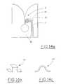
- FIG. 14 ashows a schematic front view of a first embodiment of an antenna element with a feed line according to the invention, where the feed line is equipped with a metal bridge;
- FIG. 14 bshows a first variant of a metal bridge
- FIG. 14 cshows a second variant of a metal bridge
- FIG. 15shows a metal bridge formed on a dielectric material.
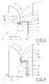
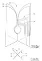
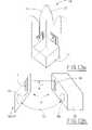
- FIG. 1a schematic view of an antenna device in the form of a tapered slot antenna element 1 a , for example of the “Vivaldi” type, is shown.
- the tapered slot antenna 1 acomprises a metal layer 2 with a slotline 3 having a first part 3 a and a second part 3 b , which slotline 3 is fed by a feed line 4 .
- An essentially two-dimensional slot cavity 5terminates the first part 3 a of the slotline 3 .
- the second part 3 b of the slotline 3transcends into an open-ended tapered slot 6 , thus forming a radiating element.
- the tapered slot antenna element 1 ais made from only one single metal layer 2 , forming a ground plane, where the feed line 4 is incorporated in this metal layer.
- the feed lineis of the type co-planar waveguide (CPW), which comprises a feeding part 7 in the form of a centre conductor 7 separated from the surrounding ground plane 2 by gaps 8 , 9 .
- the feed line 4 and its centre conductor 7intersects the slotline 3 , dividing it into the first part 3 a and the second part 3 b .
- This type of transmission lineis essentially a TEM (transverse electric and magnetic field) transmission line, similar to a coaxial line.
- This CPW feed 4makes it possible to manufacture both the feed line 4 and the tapered slot 6 in the same metal layer 2 , which may be a sheet of metal, forming a metal sheet layer 2 .
- the centre conductor 7 of the feed line 4has a first end 7 a and a second end 7 b , which first end 7 a intersects the slotline 3 .
- the second end 7 brun towards an edge 2 ′ of the metal sheet layer 2 .
- the first end 7 amay end in many ways, it may end short-circuited as shown for the antenna element 1 a in FIG. 1 , i.e. connected directly to the ground plane 2 directly after having passed the slotline 3 , dividing it into the two parts 3 a , 3 b.
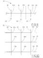
- a tapered slot antenna element 1 bis shown where the centre conductor 7 passes the slotline 3 with the length L 1 , dividing the slotline 3 into the two parts 3 a , 3 b .
- the passing length L 1 of the centre conductor 7approximately equals ⁇ g /2, i.e. one quarter of a wavelength in the material, a so called guide wavelength, where the wavelength corresponds to the centre frequency of the antenna frequency band, and the centre conductor 7 is short-circuited at its end point 7 a , resulting in that the short-circuited centre conductor 7 transforms back to be short-circuited at the slot feed point 10 as well.
- a tapered slot antenna element 1 cis shown where the centre conductor 7 passes the slotline 3 , dividing it into the two parts 3 a , 3 b .
- the passing length L 2 of the centre conductor 7approximately equals ⁇ g /4, and the centre conductor 7 is open-ended at its end point 7 a where it passes into a two-dimensional feed cavity 11 , similar to the slot cavity 5 which terminates the slotline 3 in its end that is most distant to the tapered slot 6 .
- the open-ended centre conductor 7transforms to be short-circuited at the slot feed point 10 .
- the manufacture of such an antenna element 1 a , 1 b , 1 cmay be accomplished by means of punching of a metal sheet. Since the metal sheet 2 then will be divided in two separate parts 12 , 13 , it may be necessary to mechanically support the structure at some positions in order to maintain the overall structure and function of the antenna element 1 a , 1 b , 1 c as illustrated with the antenna element 1 a in FIG. 4 , where the embodiment according to FIG. 1 is shown.
- the centre conductor 7will constitute a separate part which will have to be supported in the same way in relation to the rest of the structure.
- the supporting as shown in FIG. 4is preferably done at “non-critical” positions, i.e.
- the supporting metal or plastic retainers 14 a , 14 b , 14 cshould be placed where they do not affect the electrical field in any evident way.
- Either the material of the retainers 14 a , 14 b , 14 cis chosen to have such dielectric properties that it does not affect the electrical performance, or else the feeding line 4 is matched to adapt to the retainers 14 a , 14 b , 14 c .
- the retainers 14 a , 14 b , 14 cmay also for example form bridges (not shown) between the two parts 12 , 13 , avoiding the centre conductor 7 , and may then be made of a metal.
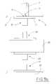
- the centre conductor 7ending at one edge 2 ′ of the metal sheet 2 as shown in detail in FIG. 5 a , may be connected to any appropriate external feeding.
- Some kind of connector 15for example an SMA connector (a screw mounted type of RF connector) or an SMB connector (a snap-fit type of RF connector) may be used.
- the inner conductor 16 of the connector 15is mounted to the second end 7 b of the centre conductor 7 by means of for example soldering, and the outer conductor 17 of the connector 15 , i.e. its ground, is mounted to the metal sheet ground plane 2 , also by means of for example soldering.
- a corresponding connector 18is mounted to an external feeding 19 , for example a distributing feeding network.
- a feeding module 20 adapted for reception and/or transmissionfor example a so-called T/R module (transmit/receive module), is placed between the antenna and the external feeding via intermediate connectors 21 , 22 , which feeding module 20 for example may be of an active, i.e. comprising amplifying units, or a passive type.
- the feeding module 20may also comprise variable phase-shifters and power attenuators.
- the feeding module 20may be connected to a control unit (not shown) for power and phase control.
- the co-planar waveguide feed that is used,is also convenient for direct integration with a feeding module 20 , omitting the first pair of connectors 17 , 21 in FIG. 5 b .
- the feeding modules 20may also be a part of the external feeding 19 , which then constitutes a feeding module in itself.
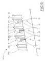
- a one-dimensional array antenna 24As shown in FIG. 6 , consisting of several of the antenna element 1 a described above may be manufactured, which array antenna 24 may have centre conductors 7 with appropriate connectors 15 attached at their edges as described above. These connectors 15 may then be attached to corresponding connectors 18 mounted at an external feeding 19 , for example a distribution network.
- Intermediate feeding modules 20as shown in FIG. 5 b (not shown in FIG. 6 ), or modules integrated in the external feeding 19 , may also be used, which modules may be adapted to feed the antenna elements 1 a in the array antenna 24 in such a way that the main lobe of the array antenna radiation pattern may be directed in different directions along the array.
- the sheetIn order to make the array antenna more stable, the sheet may be bent, forming small corresponding indents 25 a , 25 b , 25 c , 25 d , as shown in FIG. 6 .
- the array antenna 24 showed in FIG. 6is equipped with antenna elements 1 a with a CPW feeding line according to the embodiment shown in FIG. 1 .
- any one of the antenna elements 1 a , 1 b , 1 c with their respective CPW feeding embodiments described above with reference to the FIGS. 1-3may be used here and in the following array antenna examples, where the embodiment according to FIG. 1 with the tapered slot antenna element 1 a is shown.
- the retainers 14 a , 14 b , 14 c described in association with FIG. 4may wherever necessary be applied in any appropriate way in this and the following antenna embodiment examples.
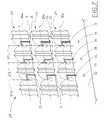
- a two-dimensional array antenna 24 ′consisting of rows 26 a , 26 b , 26 c and columns 27 a , 27 b , 27 c may be obtained, as shown in FIG. 7 .
- the rows 26 a , 26 b , 26 cmay have different displacement relative to each other depending on the desired radiation properties.
- this plurality of array antennas 24are connected to an external feeding 19 via appropriate connectors 15 , 18 , where the external feeding 19 may be a distribution net.
- Intermediate feeding modulesas shown in FIG. 5 b (not shown in FIG.
- modules integrated in the external feeding 19may also be used, which modules may be adapted to feed the antenna elements 1 a in the two-dimensional array antenna rows 26 a , 26 b , 26 c and columns 27 a , 27 b , 27 c in such a way that the main lobe of the array antenna radiation pattern may be directed in different directions along the array antenna rows 26 a , 26 b , 26 c and columns 27 a , 27 b , 27 c.
- a dual polarized antenna 28is shown.
- the dual polarized antenna element 28comprises two orthogonally arranged antenna elements 1 a′ 1 a′′ .
- the metal sheets 2 a , 2 b that constitute the dual polarized antenna 28are here placed in such a way that they cross each other.
- Corresponding mounting slots(not shown) have to be made in the metal sheets in order to allow this placing. The mounting slots will be further discussed later.
- the feeding lines 4 a , 4 bwill have to be separated vertically in order to avoid that the centre conductors 4 a , 4 b come in contact with each other in the intersection.
- the crossing point 29shown in the top view in FIG.
- the dual polarized antenna 28radiates main lobes that are orthogonal relative to each other, and may also be fed in such a way that it radiates circular polarization.
- a one-dimensional dual polarized array antenna 33 as shown in the top view in FIG. 9is obtained.
- the antenna elementsare thus arranged in orthogonal pairs 28 ′, 28 ′′, 28 ′′′, according to the dual polarized antenna element shown in FIG. 8 a and FIG. 8 b , radiating in orthogonal directions.
- Corresponding mounting slots(not shown) have to be made in the metal sheets in order to allow this placing.
- the antennas 30 , 31 , 32are placed in such a way that they cross each other.
- the crossing points 34 a , 34 b , 34 care soldered together, in order to ensure a good electrical connection.
- the indents 25 a - d shown in FIGS. 6 and 7are not shown in FIGS. 9-13 . Due to the more stable structure due to the orthogonally placed antenna elements, the indents may be omitted in the above example and in the following examples.
- a two-dimensional dual polarized array antenna 35is obtained, i.e. the antenna elements are arranged in orthogonal pairs in two dimensions, radiating in orthogonal directions.
- the metal sheets 36 , 37 , 38 ; 39 , 40 , 41are here placed in such a way that they cross each other, the crossing points 42 a , 42 b , 42 c , 42 d , 42 e , 4 f , 42 g , 42 h , 42 i may be either between each antenna element, or in the middle of each antenna element.
- Corresponding mounting slotshave to be made in the metal sheets in order to allow this placing.
- the crossing points 42 a , 42 b , 42 c , 42 d , 42 e , 42 f , 42 g , 42 h , 42 iare soldered together, in order to ensure a good electrical connection.
- a one-dimensional array antenna 24equipped with mounting slots 43 , 44 as discussed above, is shown in two different embodiments in FIG. 11 a and FIG. 11 b .
- the mounting slots 43 of one array antenna roware shown with a continuous line
- the mounting slots 44 of a corresponding array antenna roware shown with a dotted line.
- the array antenna rows with dotted line mounting slots 44are placed orthogonally onto the array antenna rows with continuous line mounting slots 43 , allowing the slots 43 , 44 to grip into each other.
- the slots 43 , 44may also be made in the middle of each tapered slotline 3 (not shown), but then the feeding lines 4 will have to be separated vertically in order to avoid that they come in contact with each other in the intersection as described above with reference to FIGS. 8 a and 8 b.
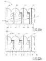
- FIG. 11 athe centre conductors 7 of the CPW feed lines 4 run to the edge 45 of the metal sheet.
- FIG. 11 bthe centre conductor 7 of the CPW feed line 4 stops before it reaches the edge 45 of the metal sheet.
- the latter configurationwill be discussed further below. It is to be noted, however, that the embodiment according to FIG. 11 b does not result in separate metal parts that have to be retained in relation to each other in some appropriate way, but instead results in a coherent structure.
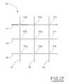
- FIG. 12another dual polarized two-dimensional antenna array 46 is shown. Punched metal sheets 47 , 48 , 49 , 50 , 51 , 52 are here arranged in a zigzag pattern, and are arranged in such a way that an arrangement similar to the embodiment according to that in FIG. 10 is obtained.
- the crossing points 53 a , 53 b , 53 c , 53 d , 53 e , 53 f , 53 g , 53 h , 53 iare here positioned between the foldings in the zigzag pattern, which foldings and crossing points 53 a , 53 b , 53 c , 53 d , 53 e , 53 f , 53 g , 53 h , 53 i may be positioned either between each antenna element or in the middle of each antenna element.
- the crossing points 53 a , 53 b , 53 c , 53 d , 53 e , 53 f , 53 g , 53 h , 53 iare soldered together, in order to ensure a good electrical connection.
- All these antenna elements in the dual polarized embodiments described aboveare, as in the previous single polarized cases, connected to an external feeding 19 , 20 via appropriate connections, where the external feeding 19 , 20 may be a distribution net which may comprise means adapted for reception and/or transmission, for example a so-called T/R module (transmit/receive module), that may be of an active or a passive type.
- the feeding 19 , 20may also comprise variable phase-shifters and power attenuators.
- the feeding 19 , 20may be connected to a control unit (not shown) for power and phase control.
- the antenna elements 1 a , 1 a′ , 1 a′′ , 1 b , 1 c , 30 , 31 , 32 in the antenna array 24 , 24 ′, 33 , 35 , 46 columns and rowsmay thus be fed in such a way that the main lobe of the array antenna radiation pattern may be directed in different directions along the array columns and rows for each one of the two polarizations.
- the antenna elements in the dual polarized embodiments described abovemay also be fed in such a way that circular polarization is obtained.
- FIG. 13 a and FIG. 13 bdisclose one possibility to feed a dual polarized array antenna 54 according to FIG. 10 or FIG. 12 having centre conductors 7 according to FIG. 11 b , not extending all the way down to the edge 45 of the metal sheet.
- FIG. 13 bthe structure is shown separated, as indicated with arrows A 1 and A 2 .
- An insertion feeding module 55essentially cubic or shaped as a rectangular parallelepiped, fitting into the space formed by the surrounding antenna 54 elements 56 , 57 , is placed in each such space formed by the array antenna 54 grid pattern.
- the insertion feeding module 55is adapted for reception and/or transmission and may for example may be of an active or a passive type.
- the insertion feeding module 55may also comprise a feeding network, variable phase-shifters and power attenuators.
- the insertion feeding module 55may be connected to a control unit for power and phase control (not shown).
- the insertion feeding module 55has at least one coupling conductor 58 for connecting the antenna element 56 , 57 centre conductor 7 , where the coupling conductor 58 has the length L 3 which essentially equals ⁇ g /4, enabling a reliable connection to be achieved. Having the length ⁇ g /4 of the coupling conductor 58 results in that there does not have to be a perfect galvanic contact between the coupling conductor 58 and the corresponding centre conductor 7 .
- the antenna element centre conductor 7 in FIG. 11 bis shown open ended, but may be short-circuited if it is compensated for in the coupling.
- the antenna structure 54may be used as a cooling flange for the insertion feeding modules 55 . Then certain corresponding areas 59 , 60 may be chosen for heat transfer from the insertion modules to the antenna structure. These areas are preferably coated with a heat-conducting substance of a known kind.
- each insertion feeding module 55Being used in a dual polarized antenna 54 as shown in FIG. 13 a , each insertion feeding module 55 have two coupling conductors (not shown), feeding two antenna elements 56 , 57 with different polarizations. This kind of feeding of the antenna elements 56 , 57 with coupling conductors 58 coupling to a centre conductor 7 may be applied for other embodiments of the invention as well.
- the insertion feeding modules 55 used in the array antenna 54may also be arranged for feeding the antenna elements 56 , 57 in such a way that circular polarization is obtained.
- the plane against which the insertion feeding modules restis no ground plane.
- the planemay be equipped with appropriate connectors that connect each insertion feeding module 55 to its feeding, for example comprising RF, power and/or control signals (not shown).
- the indents 24 a , 24 b , 24 c , 24 d of the array antenna metal sheetsmay be arranged and shaped in many way, the one indent design shown is only one example among many.
- the array antenna configuration according to FIG. 6may be made without the retainers 14 a , 14 b , 14 c shown in FIG. 4 , as the separate metal parts 21 a , 21 b , 21 c , 21 d making up the array antenna 21 may be individually fastened to the external feeding 19 in an appropriate way, for example by means of gluing. Additional stabilizing is also added by means of the connectors 15 , 18 .
- the array antennas 24 , 24 ′, 33 , 35 , 46 , 54 described abovemay be additionally supported by placing an appropriate supporting material between the metal sheet or metal sheets forming the array antenna.
- an appropriate supporting materialwould preferably be of a foam character, such as polyurethane foam, as it should be inexpensive and not cause losses and disturb the radiation pattern.
- the slot form of the antenna elementsmay vary, the tapered slot 6 may have different shapes, it may for example be widened in steps.
- the first part 3 a of the slotmay end in many ways, for example the mentioned two-dimensional cavity 5 or a short-circuit to the metal sheet layer 2 at a suitable distance from the feed point 10 .
- the manufacturing of the antenna elementsmay be performed in many ways, punching has been mentioned above. Other examples are laser-cutting, etching, machining and water-cutting. If the manufactured antenna will consist of a plurality of separated parts, these parts may first be connected by small connecting bars, allowing easy handling. When the antenna is correctly and safely mounted, these small bars may be removed.
- the antenna structuremay be etched from a piece of substrate, for example a PTFE-based substrate.
- the metalis completely removed from one side of the substrate and the metal on the other side then constitutes the antenna element.
- Another similar piece of substrate without metal on both sidesis also used, where the antenna element is squeezed between the two substrates.
- the piece of substrate without metalis used to create symmetry. As there is only one metal layer, no parallel-plate modes will be created.
- the characteristic impedance of the CPW feeding line 4will be determined by the width of the centre conductor 7 , the width of the slotline 3 and the thickness of the metal sheet 2 .
- the slotlineis preferably essentially straight, but may also be slightly tapered.
- the ground plane 2comprises two separate ground planes 61 , 62 surrounding the centre conductor 7 of a co-planar waveguide 4 .
- these surrounding ground planes 61 , 62are preferably electrically connected near a feeding point, i.e. where the centre conductor 7 intersects the slotline 3 .
- Thisis for example accomplished by means of at least one metal bridge 63 which is bent from a thin rectangular metal piece or a metal wire.
- the metal bridge 63is soldered (or glued with electrically conducting glue) to the surrounding ground planes 61 , 62 just before the slot 3 , connecting the ground planes 61 , 62 without making contact with the centre conductor 7 .
- the metal bridge 63may be bent into shape with sharp angles as shown in FIG. 14 b , where the bridge 63 is bent from a rectangular metal piece.
- the metal bridgemay also be bent more softly, following a more or less semi-circle line 63 ′, as shown in FIG. 14 c , where the bridge 63 ′ is bent from a metal wire.
- one alternative of how to accomplish a metal bridgeis to use a piece of dielectric material 64 , preferably having a box-shape with essentially perpendicular sides.
- a copper foil conductor 66runs, forming a “U”, thus having two edges 67 , 68 which are brought into electrical contact with the surrounding ground planes 61 , 62 in FIG. 14 a by means of for example soldering or gluing with electrically conducting glue.
- the conductor 66may be formed by means of for example etching, milling or screen-printing.
- the metal bridges 63 , 63 ′, 64 described aboveare only examples of how a metal bridge may accomplished, the important feature is that the ground planes 61 , 62 surrounding the centre conductor 7 of the co-planar waveguide 4 are brought into electrical contact with each other in the vicinity of the feeding point, i.e. the slot.
- the metal bridge or bridges usedshould, however, interfere with the co-planar waveguide structure as little as possible.
- metal bridges 63 , 63 ′, 64should preferably be used for all embodiments described, for those where the centre conductor of the co-planar waveguide passes the slot and continues (for example the embodiments according to FIGS. 2 and 3 ), metal bridges should be used both before and after the slot, then preferably resulting in totally four metal bridges, two on each side.
- the tapered slot antenna described in the embodimentsmay be of the type Vivaldi notch element.
- Other types of antenna elementswhich may be made in a single metal layer and fed by a feeding line according to the invention are conceivable, for example a dipole antenna of a previously known type.
Landscapes
- Variable-Direction Aerials And Aerial Arrays (AREA)
- Waveguide Aerials (AREA)
Abstract
Description
- A symmetrical antenna structure, thus lowering the cross-polarization level.
- Low losses, as no substrate is used.
- Simple construction, allowing a cost-effective manufacture, especially for dual polarized two-dimensional phased array antennas.
- Coherent rows and columns may be joined together and form a self-supporting structure.
- Lightweight as only a single metal layer is used for the antenna element.
- Active modules adapted for reception and/or transmission may be connected to the antenna elements by being fit in the spaces between the antenna elements in a dual polarized array antenna configuration, allowing the antenna structure to act as a cooling flange for the active modules.
- An additional advantage is that no static charge build-up will occur, as only a single metal layer and no dielectrics are used for the antenna element.
Claims (23)
Applications Claiming Priority (3)
| Application Number | Priority Date | Filing Date | Title |
|---|---|---|---|
| SEPCT/SE03/02102 | 2003-12-30 | ||
| PCT/SE2003/002102WO2005064747A1 (en) | 2003-12-30 | 2003-12-30 | Antenna device, and array antenna, with planar notch element feed |
| PCT/SE2004/002011WO2005064748A1 (en) | 2003-12-30 | 2004-12-27 | Antenna device and array antenna |
Publications (2)
| Publication Number | Publication Date |
|---|---|
| US20070126648A1 US20070126648A1 (en) | 2007-06-07 |
| US7403169B2true US7403169B2 (en) | 2008-07-22 |
Family
ID=34738118
Family Applications (1)
| Application Number | Title | Priority Date | Filing Date |
|---|---|---|---|
| US10/584,907Expired - Fee RelatedUS7403169B2 (en) | 2003-12-30 | 2004-12-27 | Antenna device and array antenna |
Country Status (5)
| Country | Link |
|---|---|
| US (1) | US7403169B2 (en) |
| EP (1) | EP1700359B1 (en) |
| AU (1) | AU2003294197A1 (en) |
| RU (1) | RU2359373C2 (en) |
| WO (2) | WO2005064747A1 (en) |
Cited By (132)
| Publication number | Priority date | Publication date | Assignee | Title |
|---|---|---|---|---|
| US20080023632A1 (en)* | 2006-02-13 | 2008-01-31 | Optimer Photonics, Inc. | Millimeter and sub-millimeter wave detection |
| US20080252539A1 (en)* | 2007-04-16 | 2008-10-16 | Raytheon Company | Ultra-Wideband Antenna Array with Additional Low-Frequency Resonance |
| US20080278381A1 (en)* | 2007-05-10 | 2008-11-13 | Asustek Computer Inc. | Antenna |
| US20090237315A1 (en)* | 2008-03-20 | 2009-09-24 | Shi-Lin Huang | Multi-input, multi-output antenna device |
| US7679575B1 (en)* | 2006-06-15 | 2010-03-16 | The United States Of America As Represented By The Secretary Of The Navy | Tapered slot antenna cylindrical array |
| US20140218251A1 (en)* | 2013-02-04 | 2014-08-07 | Donald P. Waschenko | Notch-Antenna Array and Method for Making Same |
| US20140354485A1 (en)* | 2013-05-30 | 2014-12-04 | Henry Cooper | Lobe antenna |
| US20150029068A1 (en)* | 2012-02-23 | 2015-01-29 | Nec Corporation | Antenna device |
| CN102013575B (en)* | 2009-09-08 | 2015-07-22 | 日立金属株式会社 | Antenna and electronic device equipped with same |
| US9478867B2 (en) | 2011-02-08 | 2016-10-25 | Xi3 | High gain frequency step horn antenna |
| US9478868B2 (en) | 2011-02-09 | 2016-10-25 | Xi3 | Corrugated horn antenna with enhanced frequency range |
| US9606577B2 (en) | 2002-10-22 | 2017-03-28 | Atd Ventures Llc | Systems and methods for providing a dynamically modular processing unit |
| US9674711B2 (en) | 2013-11-06 | 2017-06-06 | At&T Intellectual Property I, L.P. | Surface-wave communications and methods thereof |
| US9685992B2 (en) | 2014-10-03 | 2017-06-20 | At&T Intellectual Property I, L.P. | Circuit panel network and methods thereof |
| US9705610B2 (en) | 2014-10-21 | 2017-07-11 | At&T Intellectual Property I, L.P. | Transmission device with impairment compensation and methods for use therewith |
| US9705561B2 (en) | 2015-04-24 | 2017-07-11 | At&T Intellectual Property I, L.P. | Directional coupling device and methods for use therewith |
| US9729197B2 (en) | 2015-10-01 | 2017-08-08 | At&T Intellectual Property I, L.P. | Method and apparatus for communicating network management traffic over a network |
| US9735833B2 (en) | 2015-07-31 | 2017-08-15 | At&T Intellectual Property I, L.P. | Method and apparatus for communications management in a neighborhood network |
| US9742521B2 (en) | 2014-11-20 | 2017-08-22 | At&T Intellectual Property I, L.P. | Transmission device with mode division multiplexing and methods for use therewith |
| US9742462B2 (en) | 2014-12-04 | 2017-08-22 | At&T Intellectual Property I, L.P. | Transmission medium and communication interfaces and methods for use therewith |
| US9749053B2 (en) | 2015-07-23 | 2017-08-29 | At&T Intellectual Property I, L.P. | Node device, repeater and methods for use therewith |
| US9748626B2 (en) | 2015-05-14 | 2017-08-29 | At&T Intellectual Property I, L.P. | Plurality of cables having different cross-sectional shapes which are bundled together to form a transmission medium |
| US9749013B2 (en) | 2015-03-17 | 2017-08-29 | At&T Intellectual Property I, L.P. | Method and apparatus for reducing attenuation of electromagnetic waves guided by a transmission medium |
| US9769128B2 (en) | 2015-09-28 | 2017-09-19 | At&T Intellectual Property I, L.P. | Method and apparatus for encryption of communications over a network |
| US9769020B2 (en) | 2014-10-21 | 2017-09-19 | At&T Intellectual Property I, L.P. | Method and apparatus for responding to events affecting communications in a communication network |
| US9768833B2 (en) | 2014-09-15 | 2017-09-19 | At&T Intellectual Property I, L.P. | Method and apparatus for sensing a condition in a transmission medium of electromagnetic waves |
| US9780834B2 (en) | 2014-10-21 | 2017-10-03 | At&T Intellectual Property I, L.P. | Method and apparatus for transmitting electromagnetic waves |
| US9787412B2 (en) | 2015-06-25 | 2017-10-10 | At&T Intellectual Property I, L.P. | Methods and apparatus for inducing a fundamental wave mode on a transmission medium |
| US9793955B2 (en) | 2015-04-24 | 2017-10-17 | At&T Intellectual Property I, Lp | Passive electrical coupling device and methods for use therewith |
| US9793954B2 (en) | 2015-04-28 | 2017-10-17 | At&T Intellectual Property I, L.P. | Magnetic coupling device and methods for use therewith |
| US9800327B2 (en) | 2014-11-20 | 2017-10-24 | At&T Intellectual Property I, L.P. | Apparatus for controlling operations of a communication device and methods thereof |
| US9820146B2 (en) | 2015-06-12 | 2017-11-14 | At&T Intellectual Property I, L.P. | Method and apparatus for authentication and identity management of communicating devices |
| US9838896B1 (en) | 2016-12-09 | 2017-12-05 | At&T Intellectual Property I, L.P. | Method and apparatus for assessing network coverage |
| US9838078B2 (en) | 2015-07-31 | 2017-12-05 | At&T Intellectual Property I, L.P. | Method and apparatus for exchanging communication signals |
| US9847850B2 (en) | 2014-10-14 | 2017-12-19 | At&T Intellectual Property I, L.P. | Method and apparatus for adjusting a mode of communication in a communication network |
| US9847566B2 (en) | 2015-07-14 | 2017-12-19 | At&T Intellectual Property I, L.P. | Method and apparatus for adjusting a field of a signal to mitigate interference |
| US9853342B2 (en) | 2015-07-14 | 2017-12-26 | At&T Intellectual Property I, L.P. | Dielectric transmission medium connector and methods for use therewith |
| US9860075B1 (en) | 2016-08-26 | 2018-01-02 | At&T Intellectual Property I, L.P. | Method and communication node for broadband distribution |
| US9866309B2 (en) | 2015-06-03 | 2018-01-09 | At&T Intellectual Property I, Lp | Host node device and methods for use therewith |
| US9865911B2 (en) | 2015-06-25 | 2018-01-09 | At&T Intellectual Property I, L.P. | Waveguide system for slot radiating first electromagnetic waves that are combined into a non-fundamental wave mode second electromagnetic wave on a transmission medium |
| US9866276B2 (en) | 2014-10-10 | 2018-01-09 | At&T Intellectual Property I, L.P. | Method and apparatus for arranging communication sessions in a communication system |
| US9871282B2 (en) | 2015-05-14 | 2018-01-16 | At&T Intellectual Property I, L.P. | At least one transmission medium having a dielectric surface that is covered at least in part by a second dielectric |
| US9871558B2 (en) | 2014-10-21 | 2018-01-16 | At&T Intellectual Property I, L.P. | Guided-wave transmission device and methods for use therewith |
| US9871283B2 (en) | 2015-07-23 | 2018-01-16 | At&T Intellectual Property I, Lp | Transmission medium having a dielectric core comprised of plural members connected by a ball and socket configuration |
| US9876571B2 (en) | 2015-02-20 | 2018-01-23 | At&T Intellectual Property I, Lp | Guided-wave transmission device with non-fundamental mode propagation and methods for use therewith |
| US9876264B2 (en) | 2015-10-02 | 2018-01-23 | At&T Intellectual Property I, Lp | Communication system, guided wave switch and methods for use therewith |
| US9882257B2 (en) | 2015-07-14 | 2018-01-30 | At&T Intellectual Property I, L.P. | Method and apparatus for launching a wave mode that mitigates interference |
| US9887447B2 (en) | 2015-05-14 | 2018-02-06 | At&T Intellectual Property I, L.P. | Transmission medium having multiple cores and methods for use therewith |
| US9893795B1 (en) | 2016-12-07 | 2018-02-13 | At&T Intellectual Property I, Lp | Method and repeater for broadband distribution |
| US9906269B2 (en) | 2014-09-17 | 2018-02-27 | At&T Intellectual Property I, L.P. | Monitoring and mitigating conditions in a communication network |
| US9904535B2 (en) | 2015-09-14 | 2018-02-27 | At&T Intellectual Property I, L.P. | Method and apparatus for distributing software |
| US9913139B2 (en) | 2015-06-09 | 2018-03-06 | At&T Intellectual Property I, L.P. | Signal fingerprinting for authentication of communicating devices |
| US9912027B2 (en) | 2015-07-23 | 2018-03-06 | At&T Intellectual Property I, L.P. | Method and apparatus for exchanging communication signals |
| US9912033B2 (en) | 2014-10-21 | 2018-03-06 | At&T Intellectual Property I, Lp | Guided wave coupler, coupling module and methods for use therewith |
| US9911020B1 (en) | 2016-12-08 | 2018-03-06 | At&T Intellectual Property I, L.P. | Method and apparatus for tracking via a radio frequency identification device |
| US9912382B2 (en) | 2015-06-03 | 2018-03-06 | At&T Intellectual Property I, Lp | Network termination and methods for use therewith |
| US9917341B2 (en) | 2015-05-27 | 2018-03-13 | At&T Intellectual Property I, L.P. | Apparatus and method for launching electromagnetic waves and for modifying radial dimensions of the propagating electromagnetic waves |
| US9927517B1 (en) | 2016-12-06 | 2018-03-27 | At&T Intellectual Property I, L.P. | Apparatus and methods for sensing rainfall |
| US9929755B2 (en) | 2015-07-14 | 2018-03-27 | At&T Intellectual Property I, L.P. | Method and apparatus for coupling an antenna to a device |
| US9948333B2 (en) | 2015-07-23 | 2018-04-17 | At&T Intellectual Property I, L.P. | Method and apparatus for wireless communications to mitigate interference |
| US9954287B2 (en) | 2014-11-20 | 2018-04-24 | At&T Intellectual Property I, L.P. | Apparatus for converting wireless signals and electromagnetic waves and methods thereof |
| US9954286B2 (en) | 2014-10-21 | 2018-04-24 | At&T Intellectual Property I, L.P. | Guided-wave transmission device with non-fundamental mode propagation and methods for use therewith |
| US9961788B2 (en) | 2002-10-22 | 2018-05-01 | Atd Ventures, Llc | Non-peripherals processing control module having improved heat dissipating properties |
| US9967173B2 (en) | 2015-07-31 | 2018-05-08 | At&T Intellectual Property I, L.P. | Method and apparatus for authentication and identity management of communicating devices |
| US9973416B2 (en) | 2014-10-02 | 2018-05-15 | At&T Intellectual Property I, L.P. | Method and apparatus that provides fault tolerance in a communication network |
| US9973940B1 (en) | 2017-02-27 | 2018-05-15 | At&T Intellectual Property I, L.P. | Apparatus and methods for dynamic impedance matching of a guided wave launcher |
| US9991605B2 (en) | 2015-06-16 | 2018-06-05 | The Mitre Corporation | Frequency-scaled ultra-wide spectrum element |
| US9998870B1 (en) | 2016-12-08 | 2018-06-12 | At&T Intellectual Property I, L.P. | Method and apparatus for proximity sensing |
| US9997819B2 (en) | 2015-06-09 | 2018-06-12 | At&T Intellectual Property I, L.P. | Transmission medium and method for facilitating propagation of electromagnetic waves via a core |
| US9999038B2 (en) | 2013-05-31 | 2018-06-12 | At&T Intellectual Property I, L.P. | Remote distributed antenna system |
| US10009067B2 (en) | 2014-12-04 | 2018-06-26 | At&T Intellectual Property I, L.P. | Method and apparatus for configuring a communication interface |
| US10020844B2 (en) | 2016-12-06 | 2018-07-10 | T&T Intellectual Property I, L.P. | Method and apparatus for broadcast communication via guided waves |
| US10027397B2 (en) | 2016-12-07 | 2018-07-17 | At&T Intellectual Property I, L.P. | Distributed antenna system and methods for use therewith |
| US10044409B2 (en) | 2015-07-14 | 2018-08-07 | At&T Intellectual Property I, L.P. | Transmission medium and methods for use therewith |
| US10051630B2 (en) | 2013-05-31 | 2018-08-14 | At&T Intellectual Property I, L.P. | Remote distributed antenna system |
| US10056699B2 (en) | 2015-06-16 | 2018-08-21 | The Mitre Cooperation | Substrate-loaded frequency-scaled ultra-wide spectrum element |
| US10069535B2 (en) | 2016-12-08 | 2018-09-04 | At&T Intellectual Property I, L.P. | Apparatus and methods for launching electromagnetic waves having a certain electric field structure |
| US10069185B2 (en) | 2015-06-25 | 2018-09-04 | At&T Intellectual Property I, L.P. | Methods and apparatus for inducing a non-fundamental wave mode on a transmission medium |
| US10090606B2 (en) | 2015-07-15 | 2018-10-02 | At&T Intellectual Property I, L.P. | Antenna system with dielectric array and methods for use therewith |
| US10090594B2 (en) | 2016-11-23 | 2018-10-02 | At&T Intellectual Property I, L.P. | Antenna system having structural configurations for assembly |
| US10103422B2 (en) | 2016-12-08 | 2018-10-16 | At&T Intellectual Property I, L.P. | Method and apparatus for mounting network devices |
| US10135145B2 (en) | 2016-12-06 | 2018-11-20 | At&T Intellectual Property I, L.P. | Apparatus and methods for generating an electromagnetic wave along a transmission medium |
| US10139820B2 (en) | 2016-12-07 | 2018-11-27 | At&T Intellectual Property I, L.P. | Method and apparatus for deploying equipment of a communication system |
| US10148016B2 (en) | 2015-07-14 | 2018-12-04 | At&T Intellectual Property I, L.P. | Apparatus and methods for communicating utilizing an antenna array |
| US10168695B2 (en) | 2016-12-07 | 2019-01-01 | At&T Intellectual Property I, L.P. | Method and apparatus for controlling an unmanned aircraft |
| US10178445B2 (en) | 2016-11-23 | 2019-01-08 | At&T Intellectual Property I, L.P. | Methods, devices, and systems for load balancing between a plurality of waveguides |
| US10205655B2 (en) | 2015-07-14 | 2019-02-12 | At&T Intellectual Property I, L.P. | Apparatus and methods for communicating utilizing an antenna array and multiple communication paths |
| US10224634B2 (en) | 2016-11-03 | 2019-03-05 | At&T Intellectual Property I, L.P. | Methods and apparatus for adjusting an operational characteristic of an antenna |
| US10225025B2 (en) | 2016-11-03 | 2019-03-05 | At&T Intellectual Property I, L.P. | Method and apparatus for detecting a fault in a communication system |
| US10243784B2 (en) | 2014-11-20 | 2019-03-26 | At&T Intellectual Property I, L.P. | System for generating topology information and methods thereof |
| US10243270B2 (en) | 2016-12-07 | 2019-03-26 | At&T Intellectual Property I, L.P. | Beam adaptive multi-feed dielectric antenna system and methods for use therewith |
| US10264586B2 (en) | 2016-12-09 | 2019-04-16 | At&T Mobility Ii Llc | Cloud-based packet controller and methods for use therewith |
| US10285293B2 (en) | 2002-10-22 | 2019-05-07 | Atd Ventures, Llc | Systems and methods for providing a robust computer processing unit |
| US10291334B2 (en) | 2016-11-03 | 2019-05-14 | At&T Intellectual Property I, L.P. | System for detecting a fault in a communication system |
| US10298293B2 (en) | 2017-03-13 | 2019-05-21 | At&T Intellectual Property I, L.P. | Apparatus of communication utilizing wireless network devices |
| US10305190B2 (en) | 2016-12-01 | 2019-05-28 | At&T Intellectual Property I, L.P. | Reflecting dielectric antenna system and methods for use therewith |
| US10312567B2 (en) | 2016-10-26 | 2019-06-04 | At&T Intellectual Property I, L.P. | Launcher with planar strip antenna and methods for use therewith |
| US10326689B2 (en) | 2016-12-08 | 2019-06-18 | At&T Intellectual Property I, L.P. | Method and system for providing alternative communication paths |
| US10326494B2 (en) | 2016-12-06 | 2019-06-18 | At&T Intellectual Property I, L.P. | Apparatus for measurement de-embedding and methods for use therewith |
| US10340603B2 (en) | 2016-11-23 | 2019-07-02 | At&T Intellectual Property I, L.P. | Antenna system having shielded structural configurations for assembly |
| US10340601B2 (en) | 2016-11-23 | 2019-07-02 | At&T Intellectual Property I, L.P. | Multi-antenna system and methods for use therewith |
| US10340983B2 (en) | 2016-12-09 | 2019-07-02 | At&T Intellectual Property I, L.P. | Method and apparatus for surveying remote sites via guided wave communications |
| US10340573B2 (en) | 2016-10-26 | 2019-07-02 | At&T Intellectual Property I, L.P. | Launcher with cylindrical coupling device and methods for use therewith |
| US20190207287A1 (en)* | 2017-12-30 | 2019-07-04 | Georgios C. Dogiamis | Assembly and manufacturing friendly waveguide launchers |
| US10355367B2 (en) | 2015-10-16 | 2019-07-16 | At&T Intellectual Property I, L.P. | Antenna structure for exchanging wireless signals |
| US10361489B2 (en) | 2016-12-01 | 2019-07-23 | At&T Intellectual Property I, L.P. | Dielectric dish antenna system and methods for use therewith |
| US10359749B2 (en) | 2016-12-07 | 2019-07-23 | At&T Intellectual Property I, L.P. | Method and apparatus for utilities management via guided wave communication |
| US10374316B2 (en) | 2016-10-21 | 2019-08-06 | At&T Intellectual Property I, L.P. | System and dielectric antenna with non-uniform dielectric |
| US10382976B2 (en) | 2016-12-06 | 2019-08-13 | At&T Intellectual Property I, L.P. | Method and apparatus for managing wireless communications based on communication paths and network device positions |
| US10389029B2 (en) | 2016-12-07 | 2019-08-20 | At&T Intellectual Property I, L.P. | Multi-feed dielectric antenna system with core selection and methods for use therewith |
| US10389037B2 (en) | 2016-12-08 | 2019-08-20 | At&T Intellectual Property I, L.P. | Apparatus and methods for selecting sections of an antenna array and use therewith |
| US10411356B2 (en) | 2016-12-08 | 2019-09-10 | At&T Intellectual Property I, L.P. | Apparatus and methods for selectively targeting communication devices with an antenna array |
| US10439675B2 (en) | 2016-12-06 | 2019-10-08 | At&T Intellectual Property I, L.P. | Method and apparatus for repeating guided wave communication signals |
| US10446936B2 (en) | 2016-12-07 | 2019-10-15 | At&T Intellectual Property I, L.P. | Multi-feed dielectric antenna system and methods for use therewith |
| US10498044B2 (en) | 2016-11-03 | 2019-12-03 | At&T Intellectual Property I, L.P. | Apparatus for configuring a surface of an antenna |
| US10530505B2 (en) | 2016-12-08 | 2020-01-07 | At&T Intellectual Property I, L.P. | Apparatus and methods for launching electromagnetic waves along a transmission medium |
| US10535928B2 (en) | 2016-11-23 | 2020-01-14 | At&T Intellectual Property I, L.P. | Antenna system and methods for use therewith |
| US10547348B2 (en) | 2016-12-07 | 2020-01-28 | At&T Intellectual Property I, L.P. | Method and apparatus for switching transmission mediums in a communication system |
| US10601494B2 (en) | 2016-12-08 | 2020-03-24 | At&T Intellectual Property I, L.P. | Dual-band communication device and method for use therewith |
| US10637149B2 (en) | 2016-12-06 | 2020-04-28 | At&T Intellectual Property I, L.P. | Injection molded dielectric antenna and methods for use therewith |
| US10650940B2 (en) | 2015-05-15 | 2020-05-12 | At&T Intellectual Property I, L.P. | Transmission medium having a conductive material and methods for use therewith |
| US10694379B2 (en) | 2016-12-06 | 2020-06-23 | At&T Intellectual Property I, L.P. | Waveguide system with device-based authentication and methods for use therewith |
| US10727599B2 (en) | 2016-12-06 | 2020-07-28 | At&T Intellectual Property I, L.P. | Launcher with slot antenna and methods for use therewith |
| US10755542B2 (en) | 2016-12-06 | 2020-08-25 | At&T Intellectual Property I, L.P. | Method and apparatus for surveillance via guided wave communication |
| US10777873B2 (en) | 2016-12-08 | 2020-09-15 | At&T Intellectual Property I, L.P. | Method and apparatus for mounting network devices |
| US10797781B2 (en) | 2015-06-03 | 2020-10-06 | At&T Intellectual Property I, L.P. | Client node device and methods for use therewith |
| US10811767B2 (en) | 2016-10-21 | 2020-10-20 | At&T Intellectual Property I, L.P. | System and dielectric antenna with convex dielectric radome |
| US10819035B2 (en) | 2016-12-06 | 2020-10-27 | At&T Intellectual Property I, L.P. | Launcher with helical antenna and methods for use therewith |
| US10854993B2 (en) | 2017-09-18 | 2020-12-01 | The Mitre Corporation | Low-profile, wideband electronically scanned array for geo-location, communications, and radar |
| US10886625B2 (en) | 2018-08-28 | 2021-01-05 | The Mitre Corporation | Low-profile wideband antenna array configured to utilize efficient manufacturing processes |
| US10916969B2 (en) | 2016-12-08 | 2021-02-09 | At&T Intellectual Property I, L.P. | Method and apparatus for providing power using an inductive coupling |
| US10938108B2 (en) | 2016-12-08 | 2021-03-02 | At&T Intellectual Property I, L.P. | Frequency selective multi-feed dielectric antenna system and methods for use therewith |
Families Citing this family (24)
| Publication number | Priority date | Publication date | Assignee | Title |
|---|---|---|---|---|
| US7113142B2 (en)* | 2004-10-21 | 2006-09-26 | The Boeing Company | Design and fabrication methodology for a phased array antenna with integrated feed structure-conformal load-bearing concept |
| EP1684382A1 (en)* | 2005-01-19 | 2006-07-26 | Samsung Electronics Co., Ltd. | Small ultra wideband antenna having unidirectional radiation pattern |
| US20070164842A1 (en)* | 2006-01-19 | 2007-07-19 | Lumera Corporation | Electro-Optic Radiometer to Detect Radiation |
| US8077102B2 (en) | 2007-08-22 | 2011-12-13 | Bae Systems Plc | Deployable lens antenna |
| CN101609921A (en)* | 2008-06-20 | 2009-12-23 | 鸿富锦精密工业(深圳)有限公司 | Mobile communication device |
| JP5246115B2 (en)* | 2008-09-30 | 2013-07-24 | 日立電線株式会社 | ANTENNA AND ELECTRONIC DEVICE HAVING ANTENNA |
| FR2939243A1 (en)* | 2008-11-28 | 2010-06-04 | Thales Sa | Active antenna element, has ventilator configured and arranged in manner to force circulation of exterior air, where exterior air is inputted through one of faces of element and outputted through other face of element |
| US9685707B2 (en)* | 2012-05-30 | 2017-06-20 | Raytheon Company | Active electronically scanned array antenna |
| US9257747B2 (en)* | 2012-06-30 | 2016-02-09 | Taoglas Group Holdings Limited | Vivaldi-monopole antenna |
| CN104810613B (en)* | 2014-01-26 | 2018-06-26 | 华为终端(东莞)有限公司 | A kind of terminal antenna configuration and terminal |
| US9722307B2 (en) | 2014-01-26 | 2017-08-01 | Huawei Device Co., Ltd. | Terminal antenna structure and terminal |
| US10389008B2 (en) | 2015-02-26 | 2019-08-20 | Ramot At Tel-Aviv University Ltd. | Technique for improving efficiency of on-chip antennas |
| EP3199957B1 (en)* | 2016-01-29 | 2020-12-30 | Rohde & Schwarz GmbH & Co. KG | Over the air measurement module |
| US10230172B1 (en)* | 2016-02-19 | 2019-03-12 | Rockwell Collins, Inc. | Thin metal ultra-wideband antenna array systems and methods |
| CN105826667A (en)* | 2016-03-15 | 2016-08-03 | 南京信息工程大学 | Novel small Vivaldi antenna |
| CN106532270B (en)* | 2016-12-29 | 2019-08-27 | 南京信息职业技术学院 | Resistance loaded miniaturized Vivaldi antenna for electromagnetic radiation measurement system |
| CN111613864A (en)* | 2019-02-22 | 2020-09-01 | 北京小米移动软件有限公司 | Antenna modules and electronics |
| CN110174649B (en)* | 2019-05-07 | 2024-07-19 | 加特兰微电子科技(上海)有限公司 | Radio frequency front-end transceiver and vehicle-mounted radar transceiver system |
| CN111490342B (en)* | 2020-04-24 | 2021-06-01 | 电子科技大学 | Ultra-wideband dual-polarized lens antenna based on Vivaldi antenna form |
| CN113054415B (en)* | 2021-04-01 | 2022-09-13 | 北京有竹居网络技术有限公司 | Antennas and Terminals |
| CN113381183B (en)* | 2021-06-10 | 2022-01-25 | 华南理工大学 | An Antipodal Vivaldi Antenna Based on Artificial Surface Plasmons |
| CN115528426B (en)* | 2021-06-25 | 2025-04-08 | 中国移动通信集团终端有限公司 | Antenna array and router |
| CN114744419B (en)* | 2022-03-14 | 2023-05-02 | 中国电子科技集团公司第二十九研究所 | Orthogonal polarization wide bandwidth angle scanning phased array antenna |
| CN115360497B (en)* | 2022-07-22 | 2024-04-05 | 青岛大学 | A flexible wearable ultra-wideband CPW antenna and preparation method thereof |
Citations (8)
| Publication number | Priority date | Publication date | Assignee | Title |
|---|---|---|---|---|
| US4853704A (en)* | 1988-05-23 | 1989-08-01 | Ball Corporation | Notch antenna with microstrip feed |
| EP0455493A2 (en) | 1990-05-04 | 1991-11-06 | Motorola, Inc. | Tapered notch antenna |
| FR2691014A1 (en) | 1985-10-11 | 1993-11-12 | Thomson Csf | Waveguide antenna for radar ECM - has two logarithmic shaped launchers with opposite phase feed mounted in waveguide |
| US5519408A (en)* | 1991-01-22 | 1996-05-21 | Us Air Force | Tapered notch antenna using coplanar waveguide |
| US5748153A (en)* | 1994-11-08 | 1998-05-05 | Northrop Grumman Corporation | Flared conductor-backed coplanar waveguide traveling wave antenna |
| US6043785A (en)* | 1998-11-30 | 2000-03-28 | Radio Frequency Systems, Inc. | Broadband fixed-radius slot antenna arrangement |
| US6239761B1 (en)* | 1996-08-29 | 2001-05-29 | Trw Inc. | Extended dielectric material tapered slot antenna |
| US6292153B1 (en)* | 1999-08-27 | 2001-09-18 | Fantasma Network, Inc. | Antenna comprising two wideband notch regions on one coplanar substrate |
Family Cites Families (3)
| Publication number | Priority date | Publication date | Assignee | Title |
|---|---|---|---|---|
| US5142255A (en)* | 1990-05-07 | 1992-08-25 | The Texas A&M University System | Planar active endfire radiating elements and coplanar waveguide filters with wide electronic tuning bandwidth |
| JP3550859B2 (en)* | 1996-03-05 | 2004-08-04 | 三菱電機株式会社 | Tapered slot antenna |
| US6963312B2 (en)* | 2001-09-04 | 2005-11-08 | Raytheon Company | Slot for decade band tapered slot antenna, and method of making and configuring same |
- 2003
- 2003-12-30AUAU2003294197Apatent/AU2003294197A1/ennot_activeAbandoned
- 2003-12-30WOPCT/SE2003/002102patent/WO2005064747A1/enactiveApplication Filing
- 2004
- 2004-12-27USUS10/584,907patent/US7403169B2/ennot_activeExpired - Fee Related
- 2004-12-27EPEP04809184.7Apatent/EP1700359B1/ennot_activeExpired - Lifetime
- 2004-12-27WOPCT/SE2004/002011patent/WO2005064748A1/ennot_activeApplication Discontinuation
- 2004-12-27RURU2006123262/09Apatent/RU2359373C2/ennot_activeIP Right Cessation
Patent Citations (8)
| Publication number | Priority date | Publication date | Assignee | Title |
|---|---|---|---|---|
| FR2691014A1 (en) | 1985-10-11 | 1993-11-12 | Thomson Csf | Waveguide antenna for radar ECM - has two logarithmic shaped launchers with opposite phase feed mounted in waveguide |
| US4853704A (en)* | 1988-05-23 | 1989-08-01 | Ball Corporation | Notch antenna with microstrip feed |
| EP0455493A2 (en) | 1990-05-04 | 1991-11-06 | Motorola, Inc. | Tapered notch antenna |
| US5519408A (en)* | 1991-01-22 | 1996-05-21 | Us Air Force | Tapered notch antenna using coplanar waveguide |
| US5748153A (en)* | 1994-11-08 | 1998-05-05 | Northrop Grumman Corporation | Flared conductor-backed coplanar waveguide traveling wave antenna |
| US6239761B1 (en)* | 1996-08-29 | 2001-05-29 | Trw Inc. | Extended dielectric material tapered slot antenna |
| US6043785A (en)* | 1998-11-30 | 2000-03-28 | Radio Frequency Systems, Inc. | Broadband fixed-radius slot antenna arrangement |
| US6292153B1 (en)* | 1999-08-27 | 2001-09-18 | Fantasma Network, Inc. | Antenna comprising two wideband notch regions on one coplanar substrate |
Non-Patent Citations (5)
| Title |
|---|
| Dufrêne et al., Linear Antenna Array with Radiators in the Form of a Tapered Slot, Proceedings of the 14<SUP>th </SUP>International Conference on Microwaves, Radar and Wireless Communications, MIKON-2002, 2002, vol. 1, pp. 222-225. |
| International Search Report for PCT/SE04/02011 dated Apr. 18, 2005. |
| Patent Abstracts of Japan, vol. 1998, No. 1, Jan. 30, 1998, for JP 09-246849, Sep. 19, 1997. |
| Schaubert et al., Wideband Vivaldi Arrays for Large Aperture Antennas, Proceedings of the Conference held at the Astron Institute, Apr. 12-14, pp. 49-57. |
| Wu et al., Coplanar Waveguide Feed Linear Tapered Slot Antenna, Proceedings of the IEEE Antennas and Propagation International Symposium, part 1 of 2, Jun. 28-Jul. 2, 1993, vol. 1, pp. 364-367. |
Cited By (162)
| Publication number | Priority date | Publication date | Assignee | Title |
|---|---|---|---|---|
| US10849245B2 (en) | 2002-10-22 | 2020-11-24 | Atd Ventures, Llc | Systems and methods for providing a robust computer processing unit |
| US9606577B2 (en) | 2002-10-22 | 2017-03-28 | Atd Ventures Llc | Systems and methods for providing a dynamically modular processing unit |
| US11751350B2 (en) | 2002-10-22 | 2023-09-05 | Atd Ventures, Llc | Systems and methods for providing a robust computer processing unit |
| US10285293B2 (en) | 2002-10-22 | 2019-05-07 | Atd Ventures, Llc | Systems and methods for providing a robust computer processing unit |
| US9961788B2 (en) | 2002-10-22 | 2018-05-01 | Atd Ventures, Llc | Non-peripherals processing control module having improved heat dissipating properties |
| US20080023632A1 (en)* | 2006-02-13 | 2008-01-31 | Optimer Photonics, Inc. | Millimeter and sub-millimeter wave detection |
| US7486247B2 (en)* | 2006-02-13 | 2009-02-03 | Optimer Photonics, Inc. | Millimeter and sub-millimeter wave detection |
| US7679575B1 (en)* | 2006-06-15 | 2010-03-16 | The United States Of America As Represented By The Secretary Of The Navy | Tapered slot antenna cylindrical array |
| US7652631B2 (en)* | 2007-04-16 | 2010-01-26 | Raytheon Company | Ultra-wideband antenna array with additional low-frequency resonance |
| US20080252539A1 (en)* | 2007-04-16 | 2008-10-16 | Raytheon Company | Ultra-Wideband Antenna Array with Additional Low-Frequency Resonance |
| US7821461B2 (en)* | 2007-05-10 | 2010-10-26 | Asustek Computer Inc. | Antenna |
| US20080278381A1 (en)* | 2007-05-10 | 2008-11-13 | Asustek Computer Inc. | Antenna |
| US20090237315A1 (en)* | 2008-03-20 | 2009-09-24 | Shi-Lin Huang | Multi-input, multi-output antenna device |
| CN102013575B (en)* | 2009-09-08 | 2015-07-22 | 日立金属株式会社 | Antenna and electronic device equipped with same |
| US9478867B2 (en) | 2011-02-08 | 2016-10-25 | Xi3 | High gain frequency step horn antenna |
| US9478868B2 (en) | 2011-02-09 | 2016-10-25 | Xi3 | Corrugated horn antenna with enhanced frequency range |
| US20150029068A1 (en)* | 2012-02-23 | 2015-01-29 | Nec Corporation | Antenna device |
| US9472855B2 (en)* | 2012-02-23 | 2016-10-18 | Nec Corporation | Antenna device |
| US20140218251A1 (en)* | 2013-02-04 | 2014-08-07 | Donald P. Waschenko | Notch-Antenna Array and Method for Making Same |
| US9270027B2 (en)* | 2013-02-04 | 2016-02-23 | Sensor And Antenna Systems, Lansdale, Inc. | Notch-antenna array and method for making same |
| US20140354485A1 (en)* | 2013-05-30 | 2014-12-04 | Henry Cooper | Lobe antenna |
| US9450309B2 (en)* | 2013-05-30 | 2016-09-20 | Xi3 | Lobe antenna |
| US9999038B2 (en) | 2013-05-31 | 2018-06-12 | At&T Intellectual Property I, L.P. | Remote distributed antenna system |
| US10051630B2 (en) | 2013-05-31 | 2018-08-14 | At&T Intellectual Property I, L.P. | Remote distributed antenna system |
| US9674711B2 (en) | 2013-11-06 | 2017-06-06 | At&T Intellectual Property I, L.P. | Surface-wave communications and methods thereof |
| US9768833B2 (en) | 2014-09-15 | 2017-09-19 | At&T Intellectual Property I, L.P. | Method and apparatus for sensing a condition in a transmission medium of electromagnetic waves |
| US9906269B2 (en) | 2014-09-17 | 2018-02-27 | At&T Intellectual Property I, L.P. | Monitoring and mitigating conditions in a communication network |
| US10063280B2 (en) | 2014-09-17 | 2018-08-28 | At&T Intellectual Property I, L.P. | Monitoring and mitigating conditions in a communication network |
| US9973416B2 (en) | 2014-10-02 | 2018-05-15 | At&T Intellectual Property I, L.P. | Method and apparatus that provides fault tolerance in a communication network |
| US9685992B2 (en) | 2014-10-03 | 2017-06-20 | At&T Intellectual Property I, L.P. | Circuit panel network and methods thereof |
| US9866276B2 (en) | 2014-10-10 | 2018-01-09 | At&T Intellectual Property I, L.P. | Method and apparatus for arranging communication sessions in a communication system |
| US9847850B2 (en) | 2014-10-14 | 2017-12-19 | At&T Intellectual Property I, L.P. | Method and apparatus for adjusting a mode of communication in a communication network |
| US9871558B2 (en) | 2014-10-21 | 2018-01-16 | At&T Intellectual Property I, L.P. | Guided-wave transmission device and methods for use therewith |
| US9705610B2 (en) | 2014-10-21 | 2017-07-11 | At&T Intellectual Property I, L.P. | Transmission device with impairment compensation and methods for use therewith |
| US9876587B2 (en) | 2014-10-21 | 2018-01-23 | At&T Intellectual Property I, L.P. | Transmission device with impairment compensation and methods for use therewith |
| US9954286B2 (en) | 2014-10-21 | 2018-04-24 | At&T Intellectual Property I, L.P. | Guided-wave transmission device with non-fundamental mode propagation and methods for use therewith |
| US9960808B2 (en) | 2014-10-21 | 2018-05-01 | At&T Intellectual Property I, L.P. | Guided-wave transmission device and methods for use therewith |
| US9780834B2 (en) | 2014-10-21 | 2017-10-03 | At&T Intellectual Property I, L.P. | Method and apparatus for transmitting electromagnetic waves |
| US9769020B2 (en) | 2014-10-21 | 2017-09-19 | At&T Intellectual Property I, L.P. | Method and apparatus for responding to events affecting communications in a communication network |
| US9912033B2 (en) | 2014-10-21 | 2018-03-06 | At&T Intellectual Property I, Lp | Guided wave coupler, coupling module and methods for use therewith |
| US10243784B2 (en) | 2014-11-20 | 2019-03-26 | At&T Intellectual Property I, L.P. | System for generating topology information and methods thereof |
| US9800327B2 (en) | 2014-11-20 | 2017-10-24 | At&T Intellectual Property I, L.P. | Apparatus for controlling operations of a communication device and methods thereof |
| US9742521B2 (en) | 2014-11-20 | 2017-08-22 | At&T Intellectual Property I, L.P. | Transmission device with mode division multiplexing and methods for use therewith |
| US9954287B2 (en) | 2014-11-20 | 2018-04-24 | At&T Intellectual Property I, L.P. | Apparatus for converting wireless signals and electromagnetic waves and methods thereof |
| US9749083B2 (en) | 2014-11-20 | 2017-08-29 | At&T Intellectual Property I, L.P. | Transmission device with mode division multiplexing and methods for use therewith |
| US9742462B2 (en) | 2014-12-04 | 2017-08-22 | At&T Intellectual Property I, L.P. | Transmission medium and communication interfaces and methods for use therewith |
| US10009067B2 (en) | 2014-12-04 | 2018-06-26 | At&T Intellectual Property I, L.P. | Method and apparatus for configuring a communication interface |
| US9876571B2 (en) | 2015-02-20 | 2018-01-23 | At&T Intellectual Property I, Lp | Guided-wave transmission device with non-fundamental mode propagation and methods for use therewith |
| US9876570B2 (en) | 2015-02-20 | 2018-01-23 | At&T Intellectual Property I, Lp | Guided-wave transmission device with non-fundamental mode propagation and methods for use therewith |
| US9749013B2 (en) | 2015-03-17 | 2017-08-29 | At&T Intellectual Property I, L.P. | Method and apparatus for reducing attenuation of electromagnetic waves guided by a transmission medium |
| US9705561B2 (en) | 2015-04-24 | 2017-07-11 | At&T Intellectual Property I, L.P. | Directional coupling device and methods for use therewith |
| US10224981B2 (en) | 2015-04-24 | 2019-03-05 | At&T Intellectual Property I, Lp | Passive electrical coupling device and methods for use therewith |
| US9793955B2 (en) | 2015-04-24 | 2017-10-17 | At&T Intellectual Property I, Lp | Passive electrical coupling device and methods for use therewith |
| US9831912B2 (en) | 2015-04-24 | 2017-11-28 | At&T Intellectual Property I, Lp | Directional coupling device and methods for use therewith |
| US9793954B2 (en) | 2015-04-28 | 2017-10-17 | At&T Intellectual Property I, L.P. | Magnetic coupling device and methods for use therewith |
| US9871282B2 (en) | 2015-05-14 | 2018-01-16 | At&T Intellectual Property I, L.P. | At least one transmission medium having a dielectric surface that is covered at least in part by a second dielectric |
| US9748626B2 (en) | 2015-05-14 | 2017-08-29 | At&T Intellectual Property I, L.P. | Plurality of cables having different cross-sectional shapes which are bundled together to form a transmission medium |
| US9887447B2 (en) | 2015-05-14 | 2018-02-06 | At&T Intellectual Property I, L.P. | Transmission medium having multiple cores and methods for use therewith |
| US10650940B2 (en) | 2015-05-15 | 2020-05-12 | At&T Intellectual Property I, L.P. | Transmission medium having a conductive material and methods for use therewith |
| US9917341B2 (en) | 2015-05-27 | 2018-03-13 | At&T Intellectual Property I, L.P. | Apparatus and method for launching electromagnetic waves and for modifying radial dimensions of the propagating electromagnetic waves |
| US9912382B2 (en) | 2015-06-03 | 2018-03-06 | At&T Intellectual Property I, Lp | Network termination and methods for use therewith |
| US9967002B2 (en) | 2015-06-03 | 2018-05-08 | At&T Intellectual I, Lp | Network termination and methods for use therewith |
| US10797781B2 (en) | 2015-06-03 | 2020-10-06 | At&T Intellectual Property I, L.P. | Client node device and methods for use therewith |
| US10050697B2 (en) | 2015-06-03 | 2018-08-14 | At&T Intellectual Property I, L.P. | Host node device and methods for use therewith |
| US9935703B2 (en) | 2015-06-03 | 2018-04-03 | At&T Intellectual Property I, L.P. | Host node device and methods for use therewith |
| US9912381B2 (en) | 2015-06-03 | 2018-03-06 | At&T Intellectual Property I, Lp | Network termination and methods for use therewith |
| US9866309B2 (en) | 2015-06-03 | 2018-01-09 | At&T Intellectual Property I, Lp | Host node device and methods for use therewith |
| US10812174B2 (en) | 2015-06-03 | 2020-10-20 | At&T Intellectual Property I, L.P. | Client node device and methods for use therewith |
| US9913139B2 (en) | 2015-06-09 | 2018-03-06 | At&T Intellectual Property I, L.P. | Signal fingerprinting for authentication of communicating devices |
| US9997819B2 (en) | 2015-06-09 | 2018-06-12 | At&T Intellectual Property I, L.P. | Transmission medium and method for facilitating propagation of electromagnetic waves via a core |
| US9820146B2 (en) | 2015-06-12 | 2017-11-14 | At&T Intellectual Property I, L.P. | Method and apparatus for authentication and identity management of communicating devices |
| US9991605B2 (en) | 2015-06-16 | 2018-06-05 | The Mitre Corporation | Frequency-scaled ultra-wide spectrum element |
| US11069984B2 (en) | 2015-06-16 | 2021-07-20 | The Mitre Corporation | Substrate-loaded frequency-scaled ultra-wide spectrum element |
| US10056699B2 (en) | 2015-06-16 | 2018-08-21 | The Mitre Cooperation | Substrate-loaded frequency-scaled ultra-wide spectrum element |
| US10333230B2 (en) | 2015-06-16 | 2019-06-25 | The Mitre Corporation | Frequency-scaled ultra-wide spectrum element |
| US11088465B2 (en) | 2015-06-16 | 2021-08-10 | The Mitre Corporation | Substrate-loaded frequency-scaled ultra-wide spectrum element |
| US10340606B2 (en) | 2015-06-16 | 2019-07-02 | The Mitre Corporation | Frequency-scaled ultra-wide spectrum element |
| US9787412B2 (en) | 2015-06-25 | 2017-10-10 | At&T Intellectual Property I, L.P. | Methods and apparatus for inducing a fundamental wave mode on a transmission medium |
| US10069185B2 (en) | 2015-06-25 | 2018-09-04 | At&T Intellectual Property I, L.P. | Methods and apparatus for inducing a non-fundamental wave mode on a transmission medium |
| US9865911B2 (en) | 2015-06-25 | 2018-01-09 | At&T Intellectual Property I, L.P. | Waveguide system for slot radiating first electromagnetic waves that are combined into a non-fundamental wave mode second electromagnetic wave on a transmission medium |
| US10044409B2 (en) | 2015-07-14 | 2018-08-07 | At&T Intellectual Property I, L.P. | Transmission medium and methods for use therewith |
| US9882257B2 (en) | 2015-07-14 | 2018-01-30 | At&T Intellectual Property I, L.P. | Method and apparatus for launching a wave mode that mitigates interference |
| US9847566B2 (en) | 2015-07-14 | 2017-12-19 | At&T Intellectual Property I, L.P. | Method and apparatus for adjusting a field of a signal to mitigate interference |
| US10205655B2 (en) | 2015-07-14 | 2019-02-12 | At&T Intellectual Property I, L.P. | Apparatus and methods for communicating utilizing an antenna array and multiple communication paths |
| US10148016B2 (en) | 2015-07-14 | 2018-12-04 | At&T Intellectual Property I, L.P. | Apparatus and methods for communicating utilizing an antenna array |
| US9929755B2 (en) | 2015-07-14 | 2018-03-27 | At&T Intellectual Property I, L.P. | Method and apparatus for coupling an antenna to a device |
| US9853342B2 (en) | 2015-07-14 | 2017-12-26 | At&T Intellectual Property I, L.P. | Dielectric transmission medium connector and methods for use therewith |
| US10090606B2 (en) | 2015-07-15 | 2018-10-02 | At&T Intellectual Property I, L.P. | Antenna system with dielectric array and methods for use therewith |
| US9871283B2 (en) | 2015-07-23 | 2018-01-16 | At&T Intellectual Property I, Lp | Transmission medium having a dielectric core comprised of plural members connected by a ball and socket configuration |
| US9806818B2 (en) | 2015-07-23 | 2017-10-31 | At&T Intellectual Property I, Lp | Node device, repeater and methods for use therewith |
| US9948333B2 (en) | 2015-07-23 | 2018-04-17 | At&T Intellectual Property I, L.P. | Method and apparatus for wireless communications to mitigate interference |
| US9749053B2 (en) | 2015-07-23 | 2017-08-29 | At&T Intellectual Property I, L.P. | Node device, repeater and methods for use therewith |
| US9912027B2 (en) | 2015-07-23 | 2018-03-06 | At&T Intellectual Property I, L.P. | Method and apparatus for exchanging communication signals |
| US9735833B2 (en) | 2015-07-31 | 2017-08-15 | At&T Intellectual Property I, L.P. | Method and apparatus for communications management in a neighborhood network |
| US9967173B2 (en) | 2015-07-31 | 2018-05-08 | At&T Intellectual Property I, L.P. | Method and apparatus for authentication and identity management of communicating devices |
| US9838078B2 (en) | 2015-07-31 | 2017-12-05 | At&T Intellectual Property I, L.P. | Method and apparatus for exchanging communication signals |
| US9904535B2 (en) | 2015-09-14 | 2018-02-27 | At&T Intellectual Property I, L.P. | Method and apparatus for distributing software |
| US9769128B2 (en) | 2015-09-28 | 2017-09-19 | At&T Intellectual Property I, L.P. | Method and apparatus for encryption of communications over a network |
| US9729197B2 (en) | 2015-10-01 | 2017-08-08 | At&T Intellectual Property I, L.P. | Method and apparatus for communicating network management traffic over a network |
| US9876264B2 (en) | 2015-10-02 | 2018-01-23 | At&T Intellectual Property I, Lp | Communication system, guided wave switch and methods for use therewith |
| US10355367B2 (en) | 2015-10-16 | 2019-07-16 | At&T Intellectual Property I, L.P. | Antenna structure for exchanging wireless signals |
| US9860075B1 (en) | 2016-08-26 | 2018-01-02 | At&T Intellectual Property I, L.P. | Method and communication node for broadband distribution |
| US10811767B2 (en) | 2016-10-21 | 2020-10-20 | At&T Intellectual Property I, L.P. | System and dielectric antenna with convex dielectric radome |
| US10374316B2 (en) | 2016-10-21 | 2019-08-06 | At&T Intellectual Property I, L.P. | System and dielectric antenna with non-uniform dielectric |
| US10312567B2 (en) | 2016-10-26 | 2019-06-04 | At&T Intellectual Property I, L.P. | Launcher with planar strip antenna and methods for use therewith |
| US10340573B2 (en) | 2016-10-26 | 2019-07-02 | At&T Intellectual Property I, L.P. | Launcher with cylindrical coupling device and methods for use therewith |
| US10224634B2 (en) | 2016-11-03 | 2019-03-05 | At&T Intellectual Property I, L.P. | Methods and apparatus for adjusting an operational characteristic of an antenna |
| US10225025B2 (en) | 2016-11-03 | 2019-03-05 | At&T Intellectual Property I, L.P. | Method and apparatus for detecting a fault in a communication system |
| US10498044B2 (en) | 2016-11-03 | 2019-12-03 | At&T Intellectual Property I, L.P. | Apparatus for configuring a surface of an antenna |
| US10291334B2 (en) | 2016-11-03 | 2019-05-14 | At&T Intellectual Property I, L.P. | System for detecting a fault in a communication system |
| US10535928B2 (en) | 2016-11-23 | 2020-01-14 | At&T Intellectual Property I, L.P. | Antenna system and methods for use therewith |
| US10090594B2 (en) | 2016-11-23 | 2018-10-02 | At&T Intellectual Property I, L.P. | Antenna system having structural configurations for assembly |
| US10340601B2 (en) | 2016-11-23 | 2019-07-02 | At&T Intellectual Property I, L.P. | Multi-antenna system and methods for use therewith |
| US10178445B2 (en) | 2016-11-23 | 2019-01-08 | At&T Intellectual Property I, L.P. | Methods, devices, and systems for load balancing between a plurality of waveguides |
| US10340603B2 (en) | 2016-11-23 | 2019-07-02 | At&T Intellectual Property I, L.P. | Antenna system having shielded structural configurations for assembly |
| US10305190B2 (en) | 2016-12-01 | 2019-05-28 | At&T Intellectual Property I, L.P. | Reflecting dielectric antenna system and methods for use therewith |
| US10361489B2 (en) | 2016-12-01 | 2019-07-23 | At&T Intellectual Property I, L.P. | Dielectric dish antenna system and methods for use therewith |
| US10326494B2 (en) | 2016-12-06 | 2019-06-18 | At&T Intellectual Property I, L.P. | Apparatus for measurement de-embedding and methods for use therewith |
| US10382976B2 (en) | 2016-12-06 | 2019-08-13 | At&T Intellectual Property I, L.P. | Method and apparatus for managing wireless communications based on communication paths and network device positions |
| US9927517B1 (en) | 2016-12-06 | 2018-03-27 | At&T Intellectual Property I, L.P. | Apparatus and methods for sensing rainfall |
| US10819035B2 (en) | 2016-12-06 | 2020-10-27 | At&T Intellectual Property I, L.P. | Launcher with helical antenna and methods for use therewith |
| US10020844B2 (en) | 2016-12-06 | 2018-07-10 | T&T Intellectual Property I, L.P. | Method and apparatus for broadcast communication via guided waves |
| US10755542B2 (en) | 2016-12-06 | 2020-08-25 | At&T Intellectual Property I, L.P. | Method and apparatus for surveillance via guided wave communication |
| US10727599B2 (en) | 2016-12-06 | 2020-07-28 | At&T Intellectual Property I, L.P. | Launcher with slot antenna and methods for use therewith |
| US10694379B2 (en) | 2016-12-06 | 2020-06-23 | At&T Intellectual Property I, L.P. | Waveguide system with device-based authentication and methods for use therewith |
| US10637149B2 (en) | 2016-12-06 | 2020-04-28 | At&T Intellectual Property I, L.P. | Injection molded dielectric antenna and methods for use therewith |
| US10135145B2 (en) | 2016-12-06 | 2018-11-20 | At&T Intellectual Property I, L.P. | Apparatus and methods for generating an electromagnetic wave along a transmission medium |
| US10439675B2 (en) | 2016-12-06 | 2019-10-08 | At&T Intellectual Property I, L.P. | Method and apparatus for repeating guided wave communication signals |
| US10389029B2 (en) | 2016-12-07 | 2019-08-20 | At&T Intellectual Property I, L.P. | Multi-feed dielectric antenna system with core selection and methods for use therewith |
| US10547348B2 (en) | 2016-12-07 | 2020-01-28 | At&T Intellectual Property I, L.P. | Method and apparatus for switching transmission mediums in a communication system |
| US9893795B1 (en) | 2016-12-07 | 2018-02-13 | At&T Intellectual Property I, Lp | Method and repeater for broadband distribution |
| US10027397B2 (en) | 2016-12-07 | 2018-07-17 | At&T Intellectual Property I, L.P. | Distributed antenna system and methods for use therewith |
| US10139820B2 (en) | 2016-12-07 | 2018-11-27 | At&T Intellectual Property I, L.P. | Method and apparatus for deploying equipment of a communication system |
| US10446936B2 (en) | 2016-12-07 | 2019-10-15 | At&T Intellectual Property I, L.P. | Multi-feed dielectric antenna system and methods for use therewith |
| US10243270B2 (en) | 2016-12-07 | 2019-03-26 | At&T Intellectual Property I, L.P. | Beam adaptive multi-feed dielectric antenna system and methods for use therewith |
| US10359749B2 (en) | 2016-12-07 | 2019-07-23 | At&T Intellectual Property I, L.P. | Method and apparatus for utilities management via guided wave communication |
| US10168695B2 (en) | 2016-12-07 | 2019-01-01 | At&T Intellectual Property I, L.P. | Method and apparatus for controlling an unmanned aircraft |
| US10777873B2 (en) | 2016-12-08 | 2020-09-15 | At&T Intellectual Property I, L.P. | Method and apparatus for mounting network devices |
| US10389037B2 (en) | 2016-12-08 | 2019-08-20 | At&T Intellectual Property I, L.P. | Apparatus and methods for selecting sections of an antenna array and use therewith |
| US10601494B2 (en) | 2016-12-08 | 2020-03-24 | At&T Intellectual Property I, L.P. | Dual-band communication device and method for use therewith |
| US10530505B2 (en) | 2016-12-08 | 2020-01-07 | At&T Intellectual Property I, L.P. | Apparatus and methods for launching electromagnetic waves along a transmission medium |
| US10069535B2 (en) | 2016-12-08 | 2018-09-04 | At&T Intellectual Property I, L.P. | Apparatus and methods for launching electromagnetic waves having a certain electric field structure |
| US10938108B2 (en) | 2016-12-08 | 2021-03-02 | At&T Intellectual Property I, L.P. | Frequency selective multi-feed dielectric antenna system and methods for use therewith |
| US9911020B1 (en) | 2016-12-08 | 2018-03-06 | At&T Intellectual Property I, L.P. | Method and apparatus for tracking via a radio frequency identification device |
| US10916969B2 (en) | 2016-12-08 | 2021-02-09 | At&T Intellectual Property I, L.P. | Method and apparatus for providing power using an inductive coupling |
| US10326689B2 (en) | 2016-12-08 | 2019-06-18 | At&T Intellectual Property I, L.P. | Method and system for providing alternative communication paths |
| US10411356B2 (en) | 2016-12-08 | 2019-09-10 | At&T Intellectual Property I, L.P. | Apparatus and methods for selectively targeting communication devices with an antenna array |
| US10103422B2 (en) | 2016-12-08 | 2018-10-16 | At&T Intellectual Property I, L.P. | Method and apparatus for mounting network devices |
| US9998870B1 (en) | 2016-12-08 | 2018-06-12 | At&T Intellectual Property I, L.P. | Method and apparatus for proximity sensing |
| US10340983B2 (en) | 2016-12-09 | 2019-07-02 | At&T Intellectual Property I, L.P. | Method and apparatus for surveying remote sites via guided wave communications |
| US10264586B2 (en) | 2016-12-09 | 2019-04-16 | At&T Mobility Ii Llc | Cloud-based packet controller and methods for use therewith |
| US9838896B1 (en) | 2016-12-09 | 2017-12-05 | At&T Intellectual Property I, L.P. | Method and apparatus for assessing network coverage |
| US9973940B1 (en) | 2017-02-27 | 2018-05-15 | At&T Intellectual Property I, L.P. | Apparatus and methods for dynamic impedance matching of a guided wave launcher |
| US10298293B2 (en) | 2017-03-13 | 2019-05-21 | At&T Intellectual Property I, L.P. | Apparatus of communication utilizing wireless network devices |
| US10854993B2 (en) | 2017-09-18 | 2020-12-01 | The Mitre Corporation | Low-profile, wideband electronically scanned array for geo-location, communications, and radar |
| US12003030B2 (en) | 2017-09-18 | 2024-06-04 | The Mitre Corporation | Low-profile, wideband electronically scanned array for integrated geo-location, communications, and radar |
| US10468737B2 (en)* | 2017-12-30 | 2019-11-05 | Intel Corporation | Assembly and manufacturing friendly waveguide launchers |
| US20190207287A1 (en)* | 2017-12-30 | 2019-07-04 | Georgios C. Dogiamis | Assembly and manufacturing friendly waveguide launchers |
| US10886625B2 (en) | 2018-08-28 | 2021-01-05 | The Mitre Corporation | Low-profile wideband antenna array configured to utilize efficient manufacturing processes |
| US20210111498A1 (en)* | 2018-08-28 | 2021-04-15 | The Mitre Corporation | Low-profile wideband antenna array configured to utilize efficient manufacturing processes |
| US11670868B2 (en)* | 2018-08-28 | 2023-06-06 | The Mitre Corporation | Low-profile wideband antenna array configured to utilize efficient manufacturing processes |
| US12051854B2 (en) | 2018-08-28 | 2024-07-30 | The Mitre Corporation | Low-profile wideband antenna array configured to utilize efficient manufacturing processes |
Also Published As
| Publication number | Publication date |
|---|---|
| EP1700359B1 (en) | 2014-04-02 |
| US20070126648A1 (en) | 2007-06-07 |
| WO2005064748A1 (en) | 2005-07-14 |
| RU2006123262A (en) | 2008-01-10 |
| RU2359373C2 (en) | 2009-06-20 |
| WO2005064747A1 (en) | 2005-07-14 |
| AU2003294197A1 (en) | 2005-07-21 |
| EP1700359A1 (en) | 2006-09-13 |
Similar Documents
| Publication | Publication Date | Title |
|---|---|---|
| US7403169B2 (en) | Antenna device and array antenna | |
| US11862879B2 (en) | Antenna elements and array | |
| JP6730290B2 (en) | Antenna array using sandwiched radiating elements above ground plane and fed by stripline | |
| KR101982641B1 (en) | Antenna element for three polarized signals | |
| US8130162B2 (en) | Broadband multi-dipole antenna with frequency-independent radiation characteristics | |
| KR100574014B1 (en) | Broadband slot array antenna | |
| US6480167B2 (en) | Flat panel array antenna | |
| CN109494460B (en) | Dual-polarization/circularly-polarized broadband high-density antenna array with high isolation | |
| CN114284751B (en) | A large-spacing ultra-wideband tightly coupled dipole array antenna with integrated correction network | |
| US9318811B1 (en) | Methods and designs for ultra-wide band(UWB) array antennas with superior performance and attributes | |
| JP2846081B2 (en) | Triplate type planar antenna | |
| US20030112200A1 (en) | Horizontally polarized printed circuit antenna array | |
| US20240322456A1 (en) | Dual-Polarized Antenna | |
| CN115000727B (en) | A wide bandwidth angular scanning array antenna unit | |
| EP2309596B1 (en) | Dual-polarization antenna's radiating element | |
| CN214754145U (en) | Wide-beam microstrip antenna | |
| US20210194148A1 (en) | Spherical space feed for antenna array systems and methods | |
| CN116154490B (en) | Ultra-wideband tight coupling wide-angle scanning array antenna | |
| KR101679543B1 (en) | Stacked bowtie radiator with integrated balun | |
| CN217182407U (en) | Dual-polarized antenna and array | |
| US20230395998A1 (en) | A dual-polarized radiator arrangement for a mobile communication antenna and a mobile communication antenna comprising at least one dual-polarized radiator arrangement | |
| JPS6369301A (en) | Shared planar antenna for polarized wave | |
| JP2833301B2 (en) | Dual-polarized planar antenna | |
| CN112271439A (en) | A circularly polarized microstrip antenna | |
| CN117374579B (en) | A broadband end-fire circularly polarized phased array antenna |
Legal Events
| Date | Code | Title | Description |
|---|---|---|---|
| AS | Assignment | Owner name:TELEFONAKTIEBOLAGET LM ERICSSON (PUBL), SWEDEN Free format text:ASSIGNMENT OF ASSIGNORS INTEREST;ASSIGNORS:SVENSSON, BENGT;HOOK, ANDERS;JOHANSSON, JOAKIM;REEL/FRAME:020833/0859;SIGNING DATES FROM 20070823 TO 20070824 | |
| STCF | Information on status: patent grant | Free format text:PATENTED CASE | |
| CC | Certificate of correction | ||
| FPAY | Fee payment | Year of fee payment:4 | |
| AS | Assignment | Owner name:HIGHBRIDGE PRINCIPAL STRATEGIES, LLC (AS COLLATERA Free format text:LIEN;ASSIGNOR:OPTIS CELLULAR TECHNOLOGY, LLC;REEL/FRAME:031866/0697 Effective date:20131219 | |
| AS | Assignment | Owner name:WILMINGTON TRUST, NATIONAL ASSOCIATION (AS COLLATE Free format text:SECURITY AGREEMENT;ASSIGNOR:OPTIS CELLULAR TECHNOLOGY, LLC;REEL/FRAME:032167/0406 Effective date:20131219 | |
| AS | Assignment | Owner name:OPTIS CELLULAR TECHNOLOGY, LLC, TEXAS Free format text:ASSIGNMENT OF ASSIGNORS INTEREST;ASSIGNOR:CLUSTER LLC;REEL/FRAME:032326/0402 Effective date:20131219 Owner name:CLUSTER LLC, DELAWARE Free format text:ASSIGNMENT OF ASSIGNORS INTEREST;ASSIGNOR:TELEFONAKTIEBOLAGET L M ERICSSON (PUBL);REEL/FRAME:032326/0219 Effective date:20131219 | |
| AS | Assignment | Owner name:HIGHBRIDGE PRINCIPAL STRATEGIES, LLC, AS COLLATERA Free format text:ASSIGNMENT OF ASSIGNORS INTEREST;ASSIGNOR:OPTIS CELLULAR TECHNOLOGY, LLC;REEL/FRAME:032786/0546 Effective date:20140424 | |
| AS | Assignment | Owner name:HIGHBRIDGE PRINCIPAL STRATEGIES, LLC, AS COLLATERA Free format text:CORRECTIVE ASSIGNMENT TO CORRECT THE NATURE OF CONVEYANCE TO READ "SECURITY INTEREST" PREVIOUSLY RECORDED ON REEL 032786 FRAME 0546. ASSIGNOR(S) HEREBY CONFIRMS THE SECURITY INTEREST;ASSIGNOR:OPTIS CELLULAR TECHNOLOGY, LLC;REEL/FRAME:033281/0216 Effective date:20140424 | |
| FPAY | Fee payment | Year of fee payment:8 | |
| AS | Assignment | Owner name:OPTIS CELLULAR TECHNOLOGY, LLC, TEXAS Free format text:RELEASE BY SECURED PARTY;ASSIGNOR:HPS INVESTMENT PARTNERS, LLC;REEL/FRAME:039359/0916 Effective date:20160711 | |
| FEPP | Fee payment procedure | Free format text:MAINTENANCE FEE REMINDER MAILED (ORIGINAL EVENT CODE: REM.); ENTITY STATUS OF PATENT OWNER: LARGE ENTITY | |
| LAPS | Lapse for failure to pay maintenance fees | Free format text:PATENT EXPIRED FOR FAILURE TO PAY MAINTENANCE FEES (ORIGINAL EVENT CODE: EXP.); ENTITY STATUS OF PATENT OWNER: LARGE ENTITY | |
| STCH | Information on status: patent discontinuation | Free format text:PATENT EXPIRED DUE TO NONPAYMENT OF MAINTENANCE FEES UNDER 37 CFR 1.362 | |
| FP | Expired due to failure to pay maintenance fee | Effective date:20200722 |