US7403075B2 - Ultra wide band signal generator - Google Patents
Ultra wide band signal generatorDownload PDFInfo
- Publication number
- US7403075B2 US7403075B2US11/345,716US34571606AUS7403075B2US 7403075 B2US7403075 B2US 7403075B2US 34571606 AUS34571606 AUS 34571606AUS 7403075 B2US7403075 B2US 7403075B2
- Authority
- US
- United States
- Prior art keywords
- transistor
- interposed
- drain
- gate
- source
- Prior art date
- Legal status (The legal status is an assumption and is not a legal conclusion. Google has not performed a legal analysis and makes no representation as to the accuracy of the status listed.)
- Active, expires
Links
Images


Classifications
- E—FIXED CONSTRUCTIONS
- E01—CONSTRUCTION OF ROADS, RAILWAYS, OR BRIDGES
- E01C—CONSTRUCTION OF, OR SURFACES FOR, ROADS, SPORTS GROUNDS, OR THE LIKE; MACHINES OR AUXILIARY TOOLS FOR CONSTRUCTION OR REPAIR
- E01C23/00—Auxiliary devices or arrangements for constructing, repairing, reconditioning, or taking-up road or like surfaces
- E01C23/06—Devices or arrangements for working the finished surface; Devices for repairing or reconditioning the surface of damaged paving; Recycling in place or on the road
- E01C23/12—Devices or arrangements for working the finished surface; Devices for repairing or reconditioning the surface of damaged paving; Recycling in place or on the road for taking-up, tearing-up, or full-depth breaking-up paving, e.g. sett extractor
- E01C23/122—Devices or arrangements for working the finished surface; Devices for repairing or reconditioning the surface of damaged paving; Recycling in place or on the road for taking-up, tearing-up, or full-depth breaking-up paving, e.g. sett extractor with power-driven tools, e.g. oscillated hammer apparatus
- E01C23/127—Devices or arrangements for working the finished surface; Devices for repairing or reconditioning the surface of damaged paving; Recycling in place or on the road for taking-up, tearing-up, or full-depth breaking-up paving, e.g. sett extractor with power-driven tools, e.g. oscillated hammer apparatus rotary, e.g. rotary hammers
- H—ELECTRICITY
- H03—ELECTRONIC CIRCUITRY
- H03B—GENERATION OF OSCILLATIONS, DIRECTLY OR BY FREQUENCY-CHANGING, BY CIRCUITS EMPLOYING ACTIVE ELEMENTS WHICH OPERATE IN A NON-SWITCHING MANNER; GENERATION OF NOISE BY SUCH CIRCUITS
- H03B5/00—Generation of oscillations using amplifier with regenerative feedback from output to input
- H03B5/08—Generation of oscillations using amplifier with regenerative feedback from output to input with frequency-determining element comprising lumped inductance and capacitance
- H03B5/12—Generation of oscillations using amplifier with regenerative feedback from output to input with frequency-determining element comprising lumped inductance and capacitance active element in amplifier being semiconductor device
- H03B5/1231—Generation of oscillations using amplifier with regenerative feedback from output to input with frequency-determining element comprising lumped inductance and capacitance active element in amplifier being semiconductor device the amplifier comprising one or more bipolar transistors
- E—FIXED CONSTRUCTIONS
- E02—HYDRAULIC ENGINEERING; FOUNDATIONS; SOIL SHIFTING
- E02F—DREDGING; SOIL-SHIFTING
- E02F5/00—Dredgers or soil-shifting machines for special purposes
- E02F5/30—Auxiliary apparatus, e.g. for thawing, cracking, blowing-up, or other preparatory treatment of the soil
- E02F5/305—Arrangements for breaking-up hard ground
- H—ELECTRICITY
- H03—ELECTRONIC CIRCUITRY
- H03B—GENERATION OF OSCILLATIONS, DIRECTLY OR BY FREQUENCY-CHANGING, BY CIRCUITS EMPLOYING ACTIVE ELEMENTS WHICH OPERATE IN A NON-SWITCHING MANNER; GENERATION OF NOISE BY SUCH CIRCUITS
- H03B5/00—Generation of oscillations using amplifier with regenerative feedback from output to input
- H03B5/08—Generation of oscillations using amplifier with regenerative feedback from output to input with frequency-determining element comprising lumped inductance and capacitance
- H03B5/12—Generation of oscillations using amplifier with regenerative feedback from output to input with frequency-determining element comprising lumped inductance and capacitance active element in amplifier being semiconductor device
- H03B5/1203—Generation of oscillations using amplifier with regenerative feedback from output to input with frequency-determining element comprising lumped inductance and capacitance active element in amplifier being semiconductor device the amplifier being a single transistor
- H—ELECTRICITY
- H03—ELECTRONIC CIRCUITRY
- H03B—GENERATION OF OSCILLATIONS, DIRECTLY OR BY FREQUENCY-CHANGING, BY CIRCUITS EMPLOYING ACTIVE ELEMENTS WHICH OPERATE IN A NON-SWITCHING MANNER; GENERATION OF NOISE BY SUCH CIRCUITS
- H03B5/00—Generation of oscillations using amplifier with regenerative feedback from output to input
- H03B5/08—Generation of oscillations using amplifier with regenerative feedback from output to input with frequency-determining element comprising lumped inductance and capacitance
- H03B5/12—Generation of oscillations using amplifier with regenerative feedback from output to input with frequency-determining element comprising lumped inductance and capacitance active element in amplifier being semiconductor device
- H03B5/1237—Generation of oscillations using amplifier with regenerative feedback from output to input with frequency-determining element comprising lumped inductance and capacitance active element in amplifier being semiconductor device comprising means for varying the frequency of the generator
- H03B5/124—Generation of oscillations using amplifier with regenerative feedback from output to input with frequency-determining element comprising lumped inductance and capacitance active element in amplifier being semiconductor device comprising means for varying the frequency of the generator the means comprising a voltage dependent capacitance
- H—ELECTRICITY
- H03—ELECTRONIC CIRCUITRY
- H03B—GENERATION OF OSCILLATIONS, DIRECTLY OR BY FREQUENCY-CHANGING, BY CIRCUITS EMPLOYING ACTIVE ELEMENTS WHICH OPERATE IN A NON-SWITCHING MANNER; GENERATION OF NOISE BY SUCH CIRCUITS
- H03B5/00—Generation of oscillations using amplifier with regenerative feedback from output to input
- H03B5/08—Generation of oscillations using amplifier with regenerative feedback from output to input with frequency-determining element comprising lumped inductance and capacitance
- H03B5/12—Generation of oscillations using amplifier with regenerative feedback from output to input with frequency-determining element comprising lumped inductance and capacitance active element in amplifier being semiconductor device
- H03B5/1237—Generation of oscillations using amplifier with regenerative feedback from output to input with frequency-determining element comprising lumped inductance and capacitance active element in amplifier being semiconductor device comprising means for varying the frequency of the generator
- H03B5/1256—Generation of oscillations using amplifier with regenerative feedback from output to input with frequency-determining element comprising lumped inductance and capacitance active element in amplifier being semiconductor device comprising means for varying the frequency of the generator the means comprising a variable inductance
- H—ELECTRICITY
- H03—ELECTRONIC CIRCUITRY
- H03B—GENERATION OF OSCILLATIONS, DIRECTLY OR BY FREQUENCY-CHANGING, BY CIRCUITS EMPLOYING ACTIVE ELEMENTS WHICH OPERATE IN A NON-SWITCHING MANNER; GENERATION OF NOISE BY SUCH CIRCUITS
- H03B2200/00—Indexing scheme relating to details of oscillators covered by H03B
- H03B2200/006—Functional aspects of oscillators
- H03B2200/007—Generation of oscillations based on harmonic frequencies, e.g. overtone oscillators
Definitions
- the present inventionrelates to a signal generator, and more particularly to a signal generator for generating a signal at a required frequency using a harmonic signal having a frequency range in the ultra wide band (UWB).
- UWBultra wide band
- a radio frequency (RF) signal received in a receiveris converted into an intermediate frequency (IF) signal by means of a mixer 10 as shown in FIG. 1 .
- the mixer 10mixes a signal delivered from a voltage controlled oscillator (VCO) 12 with the RF signal and converts the frequency of the mixed signal into the frequency of the IF signal.
- VCOvoltage controlled oscillator
- the VCO included in the receiveris mainly used for channel selection.
- the VCOIn order to be used for band selection, the VCO must have a wider frequency control range.
- the conventional VCO shown in FIG. 2cannot control a wide frequency range using only a varactor because a great number of parasitic capacitors exist in the VCO.
- a non-linear elementgenerates harmonics with respect to a fundamental frequency f, and these harmonics are generated in a wide frequency band. Since these harmonics have very little power, the harmonics are unsuitable for oscillator signals.
- an object of the present inventionis to provide a signal generator for generating harmonic signals in a frequency range of an ultra wide band and outputting a harmonic signal having a desired frequency using a harmonic signal at a power level high enough to be used as an oscillator signal.
- Another object of the present inventionis to provide a signal generator for generating harmonic signals at a power level high enough to be used as oscillator signals, using a tunable active inductor (TAI) and outputting a harmonic component having a desired frequency using a filter.
- TAIactive inductor
- an ultra wide band signal generatorincluding an active inductor for generating harmonic signals having power strengths similar to each other within a non-linear operating range, the tunable active inductor capable of tuning to a value thereof, an oscillator for amplifying and outputting the harmonic signals generated from the active inductor by frequency-transiting the harmonic signals into high frequency bands, and a filter for selectively outputting one of the harmonic signals output from the oscillator.
- FIG. 1illustrates an internal structure of a receiver in the conventional wireless communication system
- FIG. 2illustrates the conventional VCO circuit diagram
- FIG. 3is a graph illustrating power of general harmonics
- FIG. 4is a circuit diagram illustrating an ultra wide band signal generator according to a first embodiment of the present invention
- FIG. 5is a circuit diagram equivalent to a filter module shown in FIG. 4 ;
- FIG. 6is a circuit diagram illustrating an example of a TAI shown in FIG. 4 ;
- FIG. 7is a graph illustrating power of harmonics according to an input voltage of a TAI shown in FIG. 4 ;
- FIG. 8is a view for explaining harmonics output from an oscillator shown in FIG. 4 ;
- FIG. 9is a graph illustrating that a harmonic signal having a corresponding frequency is selected by a variable capacitor C load of a filter module shown in FIG. 4 ;
- FIG. 10is a circuit diagram illustrating an ultra wide band signal generator according to the second embodiment of the present invention.
- FIG. 11illustrates output power according to frequencies with respect to a signal generator shown in FIG. 4 ;
- FIG. 12illustrates a phase noise according to the change of a fundamental frequency with respect to a signal generator shown in FIG. 4 .
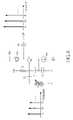
- An ultra wide band signal generatorincludes a tunable active inductor (TAI) for generating harmonic signals having an ultra wide band, an oscillator 42 for generating harmonic signals by using non-linear elements, and a filter module 41 for selecting and outputting a signal having a corresponding frequency from among the harmonic signals having the ultra wide band output from the oscillator 42 .
- TAItunable active inductor
- the TAIcan tune an inductor value thereof and is connected to a base of a transistor Q 1 of the oscillator 42 through a capacitor C 3 .
- the oscillator 42includes the transistor Q 1 , a bias voltage Bias is input to the base of the transistor Q 1 through a resistor R 1 , and capacitors C 1 and C 2 are interposed between ground and the base of the transistor of Q 1 .
- a current source I coreis connected to an emitter of the transistor Q 1 , and with capacitors C 1 and C 2 .
- an Inductor L load connected to a voltage source VDD and a capacitor C 4 connected to an output port OUTare linked with a collector of the transistor Q 1 .
- the oscillator 42 having the above structurecan output the harmonic signal input thereto from the TAI by shifting the frequency band of the harmonic signal into the frequency band of the high frequency signal generated from the oscillator 42 .
- the filter module 41is realized in such a manner that a variable capacitor C load such as a varactor is interposed between the collector of the transistor Q 1 and ground so as to select together with the inductor L load a signal having a corresponding frequency from among harmonic signals output from the collector of the transistor Q 1 .
- the filter module 41includes a parasitic capacitor C parasitic as shown in FIG. 4 . This allows the filter module 41 to be equivalent to a filter including an inductor L and a capacitor C shown in FIG. 5 .
- the TAIgenerates harmonic signals within a non-linear operation range.
- harmonic signals generated from the TAIactually have power of very little strength, it is impossible for the harmonic signals to be used in an oscillator.
- the present inventionincreases the strength of the power input to the TAI in order to generate harmonic signals having power which can be used for the oscillator 42 . If the strength of a voltage input to the TAI is increased, the strength of power of generated harmonic signals is increased. In addition, when the power of an input voltage is strong, the power of harmonic signals has strength approximate to each other.
- FIG. 6is a circuit diagram illustrating an example of the TAI.
- the TAI shown in FIG. 6includes a tunable feedback resistor in a Cascode-Grounded structure. That is, in a Gyrator structure constructed by a transistor M 4 and a transistor M 6 , the TAI has a transistor M 5 connected to a transistor M 6 in a Cascode-Grounded structure and a tunable feedback resistor R f ′ interposed between a drain of the transistor M 5 and a gate of a transistor M 4 .
- a transistor MPoperates as a current source in a PMOS type
- a transistor MNoperates as a current source in an NMOS type.
- the tunable feedback resistor R f ′includes a resistor R f and the transistor MR.
- Equation 1On the assumption that the value of the R f ′ is obtained through Equation 1, a factor Q, a peak frequency f Q of the factor Q, and a self-resonance frequency ⁇ are obtained through Equations 2 to 4, respectively.
- the g dsRdenotes an output conductance for the transistor MR.
- the g ds5 , the g ds6 , and the g dsPdenote output conductances for the transistors of M 5 , M 6 , and MP, respectively
- the C gs4 and the C gs5denote capacitances between the gates and the sources of the transistors M 4 and M 5 , respectively.
- the g mMdenotes a mutual conductance of the transistor MN
- the ⁇denotes a self-resonance frequency.
- the TAI according to the present inventionconstantly maintains the factor Q, the peak frequency f Q of the factor Q, and the self-resonance frequency ⁇ by tuning the value of the g dsP even when the value of the R f ′ increases.
- the intensity of the R f ′can be tuned by controlling the voltage V tune connected to the gate of the transistor MR.
- the value of the g dsPis tuned by controlling the V biasp connected to the gate of the transistor MP.
- the value of the TAIcan be tuned through the combination of the V biasp , the V tune , and the V biasn .
- the power of harmonic signals according to an input voltage of the TAI having the above structuremay increase and converge into a predetermined value as the input voltage increase as shown in FIG. 7 .
- the present inventionuses the above described principle. Accordingly, all harmonic signals having an ultra wide band generated from the oscillator 42 excluding the variable capacitor C load of the filter module 41 shown in FIG. 4 are shown in FIG. 8 . In other words, it can be understood from FIG. 8 that harmonic signals having power similar to each other and being generated from the TAI are amplified by the oscillator 42 so that harmonic signals having stronger power are output. As described above, according to the present invention, harmonic signals having an ultra wide band are generated using the TAI.
- FIG. 9is a graph illustrating that the filter module 41 shown in FIG. 4 selects a harmonic signal having a corresponding frequency by using the variable capacitor C load .
- the filter module 41 shown in FIG. 4selects and outputs the harmonic signal having the corresponding frequency from among harmonic signals having an ultra wide band output from the oscillator 42 by means of a transfer function of resonant load of the filter module 41 .
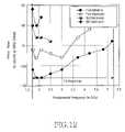
- FIGS. 11 and 12are graphs illustrating simulation results of the ultra wide band signal generator according to the present invention.
- FIG. 11illustrates output power according to frequencies
- FIG. 12illustrates a phase noise according to the change of a fundamental frequency.
- FIG. 11illustrates that the fundamental frequency must be controlled within the range of about 1.7 GHz to 5.2 GHz in order to use the harmonic signals having output power of a fundamental frequency level.
- FIG. 12illustrates frequency ranges and phase noises of fundamental frequencies and harmonic signals according to the fundamental frequencies. As shown in FIG. 12 , it can be understood that it is more efficient to use a harmonic signal having low intensity instead of a fundamental frequency having strong intensity under the condition of the same phase noise.
Landscapes
- Engineering & Computer Science (AREA)
- Mining & Mineral Resources (AREA)
- Civil Engineering (AREA)
- Structural Engineering (AREA)
- Mechanical Engineering (AREA)
- General Engineering & Computer Science (AREA)
- Architecture (AREA)
- Inductance-Capacitance Distribution Constants And Capacitance-Resistance Oscillators (AREA)
Abstract
Description
Claims (12)
Priority Applications (1)
| Application Number | Priority Date | Filing Date | Title |
|---|---|---|---|
| US11/345,716US7403075B2 (en) | 2005-02-02 | 2006-02-02 | Ultra wide band signal generator |
Applications Claiming Priority (4)
| Application Number | Priority Date | Filing Date | Title |
|---|---|---|---|
| US64928505P | 2005-02-02 | 2005-02-02 | |
| KR37291-2005 | 2005-05-03 | ||
| KR1020050037291AKR101176615B1 (en) | 2005-02-02 | 2005-05-03 | Ultra wide band signal generator |
| US11/345,716US7403075B2 (en) | 2005-02-02 | 2006-02-02 | Ultra wide band signal generator |
Publications (2)
| Publication Number | Publication Date |
|---|---|
| US20060197617A1 US20060197617A1 (en) | 2006-09-07 |
| US7403075B2true US7403075B2 (en) | 2008-07-22 |
Family
ID=37177125
Family Applications (1)
| Application Number | Title | Priority Date | Filing Date |
|---|---|---|---|
| US11/345,716Active2026-03-17US7403075B2 (en) | 2005-02-02 | 2006-02-02 | Ultra wide band signal generator |
Country Status (3)
| Country | Link |
|---|---|
| US (1) | US7403075B2 (en) |
| KR (1) | KR101176615B1 (en) |
| CN (1) | CN101106354B (en) |
Cited By (1)
| Publication number | Priority date | Publication date | Assignee | Title |
|---|---|---|---|---|
| US20080278204A1 (en)* | 2007-05-08 | 2008-11-13 | National Taiwan University Of Science And Technology | Injection-locked frequency divider embedded an active inductor |
Families Citing this family (5)
| Publication number | Priority date | Publication date | Assignee | Title |
|---|---|---|---|---|
| US7253707B2 (en)* | 2005-02-02 | 2007-08-07 | Samsung Electronics Co., Ltd. | Tunable active inductor |
| US7696833B2 (en)* | 2007-01-29 | 2010-04-13 | Fujitsu Media Devices Limited | Oscillator |
| KR100956906B1 (en)* | 2007-12-26 | 2010-05-11 | 주식회사 동부하이텍 | Inductance Implementation Using Active Inductor and Feedback Inductor |
| JP6036564B2 (en)* | 2013-06-14 | 2016-11-30 | 富士通株式会社 | Variable inductor circuit and high frequency circuit |
| CN109347442B (en)* | 2018-12-14 | 2023-09-19 | 湖南师范大学 | Miniature voltage-controlled oscillator based on tunable active inductor |
Citations (7)
| Publication number | Priority date | Publication date | Assignee | Title |
|---|---|---|---|---|
| US5347238A (en) | 1993-07-06 | 1994-09-13 | Trw Inc. | Bipolar microwave monolithic voltage controlled oscillator using active inductors |
| JPH0865050A (en) | 1994-08-25 | 1996-03-08 | Sony Corp | Oscillator |
| US5821825A (en) | 1996-11-26 | 1998-10-13 | Trw Inc. | Optically controlled oscillator |
| US20050189999A1 (en)* | 2003-12-29 | 2005-09-01 | Stmicroelectronics S.A. | Integrated electronic circuit comprising a tunable resonator |
| US20060055470A1 (en)* | 2004-08-27 | 2006-03-16 | The Hong Kong University Of Science And Technology | Integrated variable inductor |
| US20060103479A1 (en)* | 2004-11-18 | 2006-05-18 | Fabrice Paillet | Oscillator delay stage with active inductor |
| US20060158267A1 (en)* | 2004-03-22 | 2006-07-20 | Mobius Microsystems, Inc. | Inductor and capacitor-based clock generator and timing/frequency reference |
Family Cites Families (1)
| Publication number | Priority date | Publication date | Assignee | Title |
|---|---|---|---|---|
| US5623233A (en)* | 1993-11-10 | 1997-04-22 | The United States Of America As Represented By The Secretary Of The Army | Pulsed optically injection locked MESFET oscillator |
- 2005
- 2005-05-03KRKR1020050037291Apatent/KR101176615B1/ennot_activeExpired - Lifetime
- 2006
- 2006-02-02USUS11/345,716patent/US7403075B2/enactiveActive
- 2006-02-05CNCN2006100033104Apatent/CN101106354B/enactiveActive
Patent Citations (7)
| Publication number | Priority date | Publication date | Assignee | Title |
|---|---|---|---|---|
| US5347238A (en) | 1993-07-06 | 1994-09-13 | Trw Inc. | Bipolar microwave monolithic voltage controlled oscillator using active inductors |
| JPH0865050A (en) | 1994-08-25 | 1996-03-08 | Sony Corp | Oscillator |
| US5821825A (en) | 1996-11-26 | 1998-10-13 | Trw Inc. | Optically controlled oscillator |
| US20050189999A1 (en)* | 2003-12-29 | 2005-09-01 | Stmicroelectronics S.A. | Integrated electronic circuit comprising a tunable resonator |
| US20060158267A1 (en)* | 2004-03-22 | 2006-07-20 | Mobius Microsystems, Inc. | Inductor and capacitor-based clock generator and timing/frequency reference |
| US20060055470A1 (en)* | 2004-08-27 | 2006-03-16 | The Hong Kong University Of Science And Technology | Integrated variable inductor |
| US20060103479A1 (en)* | 2004-11-18 | 2006-05-18 | Fabrice Paillet | Oscillator delay stage with active inductor |
Non-Patent Citations (3)
| Title |
|---|
| Cho et al., A Novel Active Inductor and Its Application to Inductance-Controlled Oscillator, IEEE Transactions on Microwave Theory and Techniques, vol. 45, No. 8, Aug. 1997; pp. 1208-1213. |
| Kobayashi et al., A Novel Self-Oscillating HEMT-HBT Cascode VCO-Mixer Using an Active Tunable Inductor, IEEE Journal of Solid-State Circuits, vol. 33, No. 6, Jun. 1998; pp. 870-875. |
| Wu et al., A Constant Power Consumption CMOS LC Oscillator Using Improved High-Q Active Inductor With Wide Tuning-Range, The 47<SUP>th </SUP>IEEE International Symposium on Circuits and Systems, vol. 3, Jul. 25-28, 2004, pp. III347-III350. |
Cited By (2)
| Publication number | Priority date | Publication date | Assignee | Title |
|---|---|---|---|---|
| US20080278204A1 (en)* | 2007-05-08 | 2008-11-13 | National Taiwan University Of Science And Technology | Injection-locked frequency divider embedded an active inductor |
| US7683681B2 (en)* | 2007-05-08 | 2010-03-23 | National Taiwan University Of Science And Technology | Injection-locked frequency divider embedded an active inductor |
Also Published As
| Publication number | Publication date |
|---|---|
| CN101106354B (en) | 2011-02-09 |
| US20060197617A1 (en) | 2006-09-07 |
| CN101106354A (en) | 2008-01-16 |
| KR20060088805A (en) | 2006-08-07 |
| KR101176615B1 (en) | 2012-08-23 |
Similar Documents
| Publication | Publication Date | Title |
|---|---|---|
| US7239209B2 (en) | Serially RC coupled quadrature oscillator | |
| US8502614B2 (en) | Variable inductor, and oscillator and communication system using the same | |
| US7463106B2 (en) | Push-push voltage controlled oscillator for obtaining differential signals | |
| US7405632B2 (en) | Voltage-controlled oscillator, transmitter, and receiver | |
| EP1220440B1 (en) | Apparatus and method for reducing phase noise in oscillator circuits | |
| US7439811B2 (en) | Broadband low noise amplifier and RF signal amplification method of the same | |
| US6680657B2 (en) | Cross-coupled voltage controlled oscillator with improved phase noise performance | |
| US7433706B2 (en) | Multiband transmitting and receiving apparatus and method using a control voltage of phase locked loop | |
| US8792845B2 (en) | Oscillator | |
| US7403075B2 (en) | Ultra wide band signal generator | |
| US20100219896A1 (en) | Quadrature Oscillator With High Linearity | |
| US7286024B2 (en) | Voltage-controlled oscillator with differential output | |
| US20060181363A1 (en) | Parallel-structured switched variable inductor circuit | |
| US7071790B2 (en) | Method and system for a differential switched capacitor array for a voltage controlled oscillator (VCO) or a local oscillator (LO) buffer | |
| US20070123176A1 (en) | Direct conversion rf front-end transceiver and its components | |
| US20190229675A1 (en) | Multi-Stage Sub-THz Frequency Generator Incorporating Injection Locking | |
| US20090108945A1 (en) | Frequency synthesizer | |
| EP3139506B1 (en) | Apparatus and methods for using tuning information to adaptively and dynamically modify the parameters of an rf signal chain | |
| US6297706B1 (en) | Single stage voltage controlled ring oscillator | |
| EP1689074B1 (en) | Ultra wide band signal generator | |
| EP1898520B1 (en) | Voltage controlled oscillator with lc resonator circuit | |
| JPH11215024A (en) | High frequency power amplifier for radio equipment | |
| KR20090008890A (en) | Multiband Inductors and Voltage-Controlled Oscillators Using the Same | |
| KR20010063876A (en) | A low phase noise current controlled oscillator with the wide tuning range characteristics |
Legal Events
| Date | Code | Title | Description |
|---|---|---|---|
| AS | Assignment | Owner name:GEORGIA TECH RESEARCH CORPORATION, GEORGIA Free format text:ASSIGNMENT OF ASSIGNORS INTEREST;ASSIGNORS:MUKHOPADHY, RAJARSHI;NUTTINCK, SEBASTIEN;PARK, YUN-SEO;AND OTHERS;REEL/FRAME:017878/0610;SIGNING DATES FROM 20060302 TO 20060501 Owner name:SAMSUNG ELECTRONICS CO., LTD., KOREA, REPUBLIC OF Free format text:ASSIGNMENT OF ASSIGNORS INTEREST;ASSIGNORS:MUKHOPADHY, RAJARSHI;NUTTINCK, SEBASTIEN;PARK, YUN-SEO;AND OTHERS;REEL/FRAME:017878/0610;SIGNING DATES FROM 20060302 TO 20060501 | |
| AS | Assignment | Owner name:GEORGIA TECH RESEARCH CORPORATION, GEORGIA Free format text:ASSIGNMENT OF ASSIGNORS INTEREST;ASSIGNORS:MUKHOPADHYAY, RAJARSHI;NUTTINCK, SEBASTIAN;PARK, YUN-SEO;AND OTHERS;REEL/FRAME:018950/0392;SIGNING DATES FROM 20060302 TO 20060501 Owner name:SAMSUNG ELECTRONICS CO., LTD., KOREA, REPUBLIC OF Free format text:ASSIGNMENT OF ASSIGNORS INTEREST;ASSIGNORS:MUKHOPADHYAY, RAJARSHI;NUTTINCK, SEBASTIAN;PARK, YUN-SEO;AND OTHERS;REEL/FRAME:018950/0392;SIGNING DATES FROM 20060302 TO 20060501 | |
| STCF | Information on status: patent grant | Free format text:PATENTED CASE | |
| FEPP | Fee payment procedure | Free format text:PAYOR NUMBER ASSIGNED (ORIGINAL EVENT CODE: ASPN); ENTITY STATUS OF PATENT OWNER: LARGE ENTITY | |
| FEPP | Fee payment procedure | Free format text:PAYER NUMBER DE-ASSIGNED (ORIGINAL EVENT CODE: RMPN); ENTITY STATUS OF PATENT OWNER: LARGE ENTITY Free format text:PAYOR NUMBER ASSIGNED (ORIGINAL EVENT CODE: ASPN); ENTITY STATUS OF PATENT OWNER: LARGE ENTITY | |
| FPAY | Fee payment | Year of fee payment:4 | |
| FPAY | Fee payment | Year of fee payment:8 | |
| MAFP | Maintenance fee payment | Free format text:PAYMENT OF MAINTENANCE FEE, 12TH YEAR, LARGE ENTITY (ORIGINAL EVENT CODE: M1553); ENTITY STATUS OF PATENT OWNER: LARGE ENTITY Year of fee payment:12 |