US7400155B2 - Membrane probing system - Google Patents
Membrane probing systemDownload PDFInfo
- Publication number
- US7400155B2 US7400155B2US10/772,172US77217204AUS7400155B2US 7400155 B2US7400155 B2US 7400155B2US 77217204 AUS77217204 AUS 77217204AUS 7400155 B2US7400155 B2US 7400155B2
- Authority
- US
- United States
- Prior art keywords
- contact
- contacts
- membrane
- substrate
- probing
- Prior art date
- Legal status (The legal status is an assumption and is not a legal conclusion. Google has not performed a legal analysis and makes no representation as to the accuracy of the status listed.)
- Expired - Fee Related, expires
Links
Images


Classifications
- G—PHYSICS
- G01—MEASURING; TESTING
- G01R—MEASURING ELECTRIC VARIABLES; MEASURING MAGNETIC VARIABLES
- G01R1/00—Details of instruments or arrangements of the types included in groups G01R5/00 - G01R13/00 and G01R31/00
- G01R1/02—General constructional details
- G01R1/06—Measuring leads; Measuring probes
- G01R1/067—Measuring probes
- G01R1/073—Multiple probes
- G01R1/07307—Multiple probes with individual probe elements, e.g. needles, cantilever beams or bump contacts, fixed in relation to each other, e.g. bed of nails fixture or probe card
- G01R1/0735—Multiple probes with individual probe elements, e.g. needles, cantilever beams or bump contacts, fixed in relation to each other, e.g. bed of nails fixture or probe card arranged on a flexible frame or film
- H—ELECTRICITY
- H01—ELECTRIC ELEMENTS
- H01R—ELECTRICALLY-CONDUCTIVE CONNECTIONS; STRUCTURAL ASSOCIATIONS OF A PLURALITY OF MUTUALLY-INSULATED ELECTRICAL CONNECTING ELEMENTS; COUPLING DEVICES; CURRENT COLLECTORS
- H01R13/00—Details of coupling devices of the kinds covered by groups H01R12/70 or H01R24/00 - H01R33/00
- H01R13/02—Contact members
- H01R13/22—Contacts for co-operating by abutting
- H01R13/24—Contacts for co-operating by abutting resilient; resiliently-mounted
- H01R13/2407—Contacts for co-operating by abutting resilient; resiliently-mounted characterized by the resilient means
- H01R13/2414—Contacts for co-operating by abutting resilient; resiliently-mounted characterized by the resilient means conductive elastomers
- H—ELECTRICITY
- H01—ELECTRIC ELEMENTS
- H01R—ELECTRICALLY-CONDUCTIVE CONNECTIONS; STRUCTURAL ASSOCIATIONS OF A PLURALITY OF MUTUALLY-INSULATED ELECTRICAL CONNECTING ELEMENTS; COUPLING DEVICES; CURRENT COLLECTORS
- H01R13/00—Details of coupling devices of the kinds covered by groups H01R12/70 or H01R24/00 - H01R33/00
- H01R13/02—Contact members
- H01R13/22—Contacts for co-operating by abutting
- H01R13/24—Contacts for co-operating by abutting resilient; resiliently-mounted
- H01R13/2464—Contacts for co-operating by abutting resilient; resiliently-mounted characterized by the contact point
- H—ELECTRICITY
- H01—ELECTRIC ELEMENTS
- H01R—ELECTRICALLY-CONDUCTIVE CONNECTIONS; STRUCTURAL ASSOCIATIONS OF A PLURALITY OF MUTUALLY-INSULATED ELECTRICAL CONNECTING ELEMENTS; COUPLING DEVICES; CURRENT COLLECTORS
- H01R43/00—Apparatus or processes specially adapted for manufacturing, assembling, maintaining, or repairing of line connectors or current collectors or for joining electric conductors
- H01R43/16—Apparatus or processes specially adapted for manufacturing, assembling, maintaining, or repairing of line connectors or current collectors or for joining electric conductors for manufacturing contact members, e.g. by punching and by bending
- G—PHYSICS
- G01—MEASURING; TESTING
- G01R—MEASURING ELECTRIC VARIABLES; MEASURING MAGNETIC VARIABLES
- G01R1/00—Details of instruments or arrangements of the types included in groups G01R5/00 - G01R13/00 and G01R31/00
- G01R1/02—General constructional details
- G01R1/06—Measuring leads; Measuring probes
- G01R1/067—Measuring probes
- G01R1/06711—Probe needles; Cantilever beams; "Bump" contacts; Replaceable probe pins
- G01R1/06733—Geometry aspects
- G01R1/06738—Geometry aspects related to tip portion
- G—PHYSICS
- G01—MEASURING; TESTING
- G01R—MEASURING ELECTRIC VARIABLES; MEASURING MAGNETIC VARIABLES
- G01R3/00—Apparatus or processes specially adapted for the manufacture or maintenance of measuring instruments, e.g. of probe tips
- H—ELECTRICITY
- H05—ELECTRIC TECHNIQUES NOT OTHERWISE PROVIDED FOR
- H05K—PRINTED CIRCUITS; CASINGS OR CONSTRUCTIONAL DETAILS OF ELECTRIC APPARATUS; MANUFACTURE OF ASSEMBLAGES OF ELECTRICAL COMPONENTS
- H05K3/00—Apparatus or processes for manufacturing printed circuits
- H05K3/10—Apparatus or processes for manufacturing printed circuits in which conductive material is applied to the insulating support in such a manner as to form the desired conductive pattern
- H05K3/20—Apparatus or processes for manufacturing printed circuits in which conductive material is applied to the insulating support in such a manner as to form the desired conductive pattern by affixing prefabricated conductor pattern
- H—ELECTRICITY
- H05—ELECTRIC TECHNIQUES NOT OTHERWISE PROVIDED FOR
- H05K—PRINTED CIRCUITS; CASINGS OR CONSTRUCTIONAL DETAILS OF ELECTRIC APPARATUS; MANUFACTURE OF ASSEMBLAGES OF ELECTRICAL COMPONENTS
- H05K3/00—Apparatus or processes for manufacturing printed circuits
- H05K3/40—Forming printed elements for providing electric connections to or between printed circuits
- H05K3/4007—Surface contacts, e.g. bumps
- Y—GENERAL TAGGING OF NEW TECHNOLOGICAL DEVELOPMENTS; GENERAL TAGGING OF CROSS-SECTIONAL TECHNOLOGIES SPANNING OVER SEVERAL SECTIONS OF THE IPC; TECHNICAL SUBJECTS COVERED BY FORMER USPC CROSS-REFERENCE ART COLLECTIONS [XRACs] AND DIGESTS
- Y10—TECHNICAL SUBJECTS COVERED BY FORMER USPC
- Y10T—TECHNICAL SUBJECTS COVERED BY FORMER US CLASSIFICATION
- Y10T29/00—Metal working
- Y10T29/49—Method of mechanical manufacture
- Y10T29/49002—Electrical device making
- Y10T29/49004—Electrical device making including measuring or testing of device or component part
- Y—GENERAL TAGGING OF NEW TECHNOLOGICAL DEVELOPMENTS; GENERAL TAGGING OF CROSS-SECTIONAL TECHNOLOGIES SPANNING OVER SEVERAL SECTIONS OF THE IPC; TECHNICAL SUBJECTS COVERED BY FORMER USPC CROSS-REFERENCE ART COLLECTIONS [XRACs] AND DIGESTS
- Y10—TECHNICAL SUBJECTS COVERED BY FORMER USPC
- Y10T—TECHNICAL SUBJECTS COVERED BY FORMER US CLASSIFICATION
- Y10T29/00—Metal working
- Y10T29/49—Method of mechanical manufacture
- Y10T29/49002—Electrical device making
- Y10T29/49117—Conductor or circuit manufacturing
- Y10T29/49121—Beam lead frame or beam lead device
- Y—GENERAL TAGGING OF NEW TECHNOLOGICAL DEVELOPMENTS; GENERAL TAGGING OF CROSS-SECTIONAL TECHNOLOGIES SPANNING OVER SEVERAL SECTIONS OF THE IPC; TECHNICAL SUBJECTS COVERED BY FORMER USPC CROSS-REFERENCE ART COLLECTIONS [XRACs] AND DIGESTS
- Y10—TECHNICAL SUBJECTS COVERED BY FORMER USPC
- Y10T—TECHNICAL SUBJECTS COVERED BY FORMER US CLASSIFICATION
- Y10T29/00—Metal working
- Y10T29/49—Method of mechanical manufacture
- Y10T29/49002—Electrical device making
- Y10T29/49117—Conductor or circuit manufacturing
- Y10T29/49124—On flat or curved insulated base, e.g., printed circuit, etc.
- Y10T29/4913—Assembling to base an electrical component, e.g., capacitor, etc.
- Y10T29/49139—Assembling to base an electrical component, e.g., capacitor, etc. by inserting component lead or terminal into base aperture
- Y—GENERAL TAGGING OF NEW TECHNOLOGICAL DEVELOPMENTS; GENERAL TAGGING OF CROSS-SECTIONAL TECHNOLOGIES SPANNING OVER SEVERAL SECTIONS OF THE IPC; TECHNICAL SUBJECTS COVERED BY FORMER USPC CROSS-REFERENCE ART COLLECTIONS [XRACs] AND DIGESTS
- Y10—TECHNICAL SUBJECTS COVERED BY FORMER USPC
- Y10T—TECHNICAL SUBJECTS COVERED BY FORMER US CLASSIFICATION
- Y10T29/00—Metal working
- Y10T29/49—Method of mechanical manufacture
- Y10T29/49002—Electrical device making
- Y10T29/49117—Conductor or circuit manufacturing
- Y10T29/49124—On flat or curved insulated base, e.g., printed circuit, etc.
- Y10T29/49155—Manufacturing circuit on or in base
- Y10T29/49165—Manufacturing circuit on or in base by forming conductive walled aperture in base
- Y—GENERAL TAGGING OF NEW TECHNOLOGICAL DEVELOPMENTS; GENERAL TAGGING OF CROSS-SECTIONAL TECHNOLOGIES SPANNING OVER SEVERAL SECTIONS OF THE IPC; TECHNICAL SUBJECTS COVERED BY FORMER USPC CROSS-REFERENCE ART COLLECTIONS [XRACs] AND DIGESTS
- Y10—TECHNICAL SUBJECTS COVERED BY FORMER USPC
- Y10T—TECHNICAL SUBJECTS COVERED BY FORMER US CLASSIFICATION
- Y10T29/00—Metal working
- Y10T29/49—Method of mechanical manufacture
- Y10T29/49002—Electrical device making
- Y10T29/49117—Conductor or circuit manufacturing
- Y10T29/49169—Assembling electrical component directly to terminal or elongated conductor
- Y—GENERAL TAGGING OF NEW TECHNOLOGICAL DEVELOPMENTS; GENERAL TAGGING OF CROSS-SECTIONAL TECHNOLOGIES SPANNING OVER SEVERAL SECTIONS OF THE IPC; TECHNICAL SUBJECTS COVERED BY FORMER USPC CROSS-REFERENCE ART COLLECTIONS [XRACs] AND DIGESTS
- Y10—TECHNICAL SUBJECTS COVERED BY FORMER USPC
- Y10T—TECHNICAL SUBJECTS COVERED BY FORMER US CLASSIFICATION
- Y10T29/00—Metal working
- Y10T29/49—Method of mechanical manufacture
- Y10T29/49002—Electrical device making
- Y10T29/49117—Conductor or circuit manufacturing
- Y10T29/49174—Assembling terminal to elongated conductor
- Y—GENERAL TAGGING OF NEW TECHNOLOGICAL DEVELOPMENTS; GENERAL TAGGING OF CROSS-SECTIONAL TECHNOLOGIES SPANNING OVER SEVERAL SECTIONS OF THE IPC; TECHNICAL SUBJECTS COVERED BY FORMER USPC CROSS-REFERENCE ART COLLECTIONS [XRACs] AND DIGESTS
- Y10—TECHNICAL SUBJECTS COVERED BY FORMER USPC
- Y10T—TECHNICAL SUBJECTS COVERED BY FORMER US CLASSIFICATION
- Y10T29/00—Metal working
- Y10T29/49—Method of mechanical manufacture
- Y10T29/49002—Electrical device making
- Y10T29/49117—Conductor or circuit manufacturing
- Y10T29/49204—Contact or terminal manufacturing
- Y10T29/49208—Contact or terminal manufacturing by assembling plural parts
- Y10T29/49218—Contact or terminal manufacturing by assembling plural parts with deforming
- Y—GENERAL TAGGING OF NEW TECHNOLOGICAL DEVELOPMENTS; GENERAL TAGGING OF CROSS-SECTIONAL TECHNOLOGIES SPANNING OVER SEVERAL SECTIONS OF THE IPC; TECHNICAL SUBJECTS COVERED BY FORMER USPC CROSS-REFERENCE ART COLLECTIONS [XRACs] AND DIGESTS
- Y10—TECHNICAL SUBJECTS COVERED BY FORMER USPC
- Y10T—TECHNICAL SUBJECTS COVERED BY FORMER US CLASSIFICATION
- Y10T29/00—Metal working
- Y10T29/49—Method of mechanical manufacture
- Y10T29/49815—Disassembling
- Y10T29/49822—Disassembling by applying force
- Y10T29/49824—Disassembling by applying force to elastically deform work part or connector
- Y—GENERAL TAGGING OF NEW TECHNOLOGICAL DEVELOPMENTS; GENERAL TAGGING OF CROSS-SECTIONAL TECHNOLOGIES SPANNING OVER SEVERAL SECTIONS OF THE IPC; TECHNICAL SUBJECTS COVERED BY FORMER USPC CROSS-REFERENCE ART COLLECTIONS [XRACs] AND DIGESTS
- Y10—TECHNICAL SUBJECTS COVERED BY FORMER USPC
- Y10T—TECHNICAL SUBJECTS COVERED BY FORMER US CLASSIFICATION
- Y10T29/00—Metal working
- Y10T29/49—Method of mechanical manufacture
- Y10T29/49826—Assembling or joining
- Y—GENERAL TAGGING OF NEW TECHNOLOGICAL DEVELOPMENTS; GENERAL TAGGING OF CROSS-SECTIONAL TECHNOLOGIES SPANNING OVER SEVERAL SECTIONS OF THE IPC; TECHNICAL SUBJECTS COVERED BY FORMER USPC CROSS-REFERENCE ART COLLECTIONS [XRACs] AND DIGESTS
- Y10—TECHNICAL SUBJECTS COVERED BY FORMER USPC
- Y10T—TECHNICAL SUBJECTS COVERED BY FORMER US CLASSIFICATION
- Y10T29/00—Metal working
- Y10T29/53—Means to assemble or disassemble
- Y10T29/53478—Means to assemble or disassemble with magazine supply
- Y10T29/53487—Assembling means comprising hand-manipulatable implement
- Y10T29/53509—Means to assemble tyre stud into tyre tread
Definitions
- the present inventionrelates to probe assemblies of the type commonly used for testing integrated circuits (IC) and, in particular, the present invention relates to a membrane probing assembly having contacts which scrub, in a locally controlled manner, across the respective input/output conductors of each device so as to reliably wipe clear the surface oxides that are normally found on those conductors thereby ensuring good electrical connection between the probing assembly and each device.
- ICintegrated circuits
- One typical procedureis to support the wafer on a flat stage or “chuck” and to move the wafer in X, Y and Z directions relative to the head of the probing assembly so that the contacts on the probing assembly move from die to die for consecutive engagement with each die. Respective signal, power and ground lines are run to the probing assembly from the test instrumentation thus enabling each circuit to be sequentially connected to the test instrumentation.
- One conventional type of probing assembly used for testing integrated circuitsprovides contacts that are configured as needle-like tips. These tips are mounted about a central opening formed in a probe card so as to radially converge inwardly and downwardly through the opening. When the wafer is raised beyond that point where the pads on the wafer first come into contact with these tips, the tips flex upwardly so as to skate for-wardly across their respective pads thereby removing oxide buildup on the pads.
- a second type of probing assemblyuses a flexible membrane structure for supporting the probing contacts.
- lead lines of well-defined geometryare formed on one or more plies of flexible insulative film, such as polyimide or MYLARTM. If separate plies are used, these plies are bonded together to form, for example, a multilayered transmission line structure.
- each conductive lineis terminated by a respective probing contact which is formed on, and projects outwardly from, an outer face of the membrane.
- These probing contactsare arranged in a predetermined pattern that matches the pattern of the device pads and typically are formed as upraised bumps for probing the flat surfaces conventionally defined by the pads.
- the inner face of the membraneis supported on a supporting structure.
- This structurecan take the form, for example, of a truncated pyramid, in which case the inner face of the center portion of the membrane is supported on the truncated end of the support while the marginal portions of the membrane are drawn away from the center portion at an angle thereto so as to clear any upright components that may surround the pads on the device.
- Rath European Patent Pub. No. 259,163A2One conventional form of membrane probing assembly, for example, is exemplified shown in Rath European Patent Pub. No. 259,163A2.
- This devicehas the central portion of the sheet-like membrane mounted directly against a rigid support.
- This rigid supportis connected by a resilient member comprising an elastomeric or rubber block to the main body of the assembly so that the membrane can tilt to match the tilt of the device.
- 4,918,383shows a closely related device wherein radially extending leaf springs permit vertical axis movement of the rigid support while preventing it from tilting so that there is no slippage or “misalignment” of the contact bumps on the pads and further so that the entire membrane will shift slightly in the horizontal plane to allow the contacts to “scrub” across their respective pads in order to clear surface oxides from these pads.
- a second conventional form of membrane probing assemblyis exemplified by the device shown in Barsotti European Patent Pub. No. 304,868A2.
- This deviceprovides a flexible backing for the central or contact-carrying portion of the flexible membrane.
- the membraneIn Barsotti, the membrane is directly backed by an elastomeric member and this member, in turn, is backed by a rigid support so that minor height variations between the contacts or pads can be accommodated.
- the contactsmay be limited to movement along the Z-axis in order to prevent slippage and resulting misalignment between the contacts and pads during engagement.
- the rigid support underlying the elastomeric memberis fixed in position although it is also possible to mount the support for Z-axis movement in the manner shown in Huff U.S. Pat. No. 4,980,637.
- Pad damageis likely to occur with this type of design, however, because a certain amount of tilt is typically present between the contacts and the device, and those contacts angled closest to the device will ordinarily develop much higher contact pressures than those which are angled away.
- each row of contactsis supported by the end of a respective L-shaped arm so that when the contacts in a row engage their respective pads, the corresponding arm flexes upwardly and causes the row of contacts to laterally scrub simultaneously across their respective pads.
- this tiltwill cause the contacts angled closest to the device to scrub further than those angled further away.
- the shorter contactswill be forced to move in their scrub directions before they have had the opportunity to engage their respective pads due to the controlling scrub action of their neighboring contacts.
- a further disadvantage of the Crumly deviceis that the contacts nearer to the center of the membrane will scrub less than those nearer to the periphery so that scrub effectiveness will vary with contact position.
- each contactconstitutes a spring metal finger, and each finger is mounted so as to extend in a cantilevered manner away from the underlying membrane at a predetermined angle relative to the membrane.
- a similar configurationis shown in Higgins U.S. Pat. No. 5,521,518. It is difficult, however, to originally position these fingers so that they all terminate in a common plane, particularly if a high density pattern is required. Moreover, these fingers are easily bent out of position during use and cannot easily be rebent back to their original position. Hence, certain ones of the fingers are likely to touch down before other ones of the fingers, and scrub pressures and distances are likely to be different for different fingers.
- Evansat least, is there an adequate mechanism for tolerating a minor degree of tilt between the fingers and pads.
- Evanssuggests roughening the surface of each finger to improve the quality of electrical connection, this roughening can cause undue abrasion and damage to the pad surfaces.
- Yet a further disadvantage of the contact fingers shown in both Evans and Higginsis that such fingers are subject to fatigue and failure after a relatively low number of “touchdowns” or duty cycles due to repeated bending and stressing.
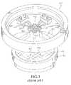
- Cascade Microtech, Inc. of Beaverton, Oregonhas developed a probe head 40 for mounting a membrane probing assembly 42 .
- the high-speed digital lines 48 and/or shielded transmission lines 50 of the probe headare connected to the input/output ports of the test instrumentation by a suitable cable assembly, and the chuck 51 which supports the wafer is moved in mutually perpendicular X,Y,Z directions in order to bring the pads of the die area into pressing engagement with the contacts included on the lower contacting portion of the membrane probing assembly.
- the probe head 40includes a probe card 52 on which the data/signal lines 48 and 50 are arranged.
- the membrane probing assembly 42includes a support element 54 formed of incompressible material such as a hard polymer. This element is detachably connected to the upper side of the probe card by four Allen screws 56 and corresponding nuts 58 (each screw passes through a respective attachment arm 60 of the support element, and a separate backing element 62 evenly distributes the clamping pressure of the screws over the entire back side of the supporting element).
- different probing assemblies having different contact arrangementscan be quickly substituted for each other as needed for probing different devices.
- the support element 54includes a rearward base portion 64 to which the attachment arms 60 are integrally joined. Also included on the support element 54 is a forward support or plunger 66 that projects outwardly from the flat base portion. This forward support has angled sides 68 that converge toward a flat support surface 70 so as to give the forward support the shape of a truncated pyramid.
- a flexible membrane assembly 72is attached to the support after being aligned by means of alignment pins 74 included on the base portion.
- This flexible membrane assemblyis formed by one or more plies of insulative sheeting such as KAPTONTM sold by E.I. Du Pont de Nemours or other polyimide film, and flexible conductive layers or strips are provided between or on these plies to form the data/signal lines 76 .
- the forward support 66protrudes through a central opening 78 in the probe card so as to present the contacts which are arranged on a central region 80 of the flexible membrane assembly in suitable position for pressing engagement with the pads of the device under test.
- the membrane assemblyincludes radially extending arm segments 82 that are separated by inwardly curving edges 84 that give the assembly the shape of a formee cross, and these segments extend in an inclined manner along the angled sides 68 thereby clearing any upright components surrounding the pads.
- a series of contact pads 86terminate the data/signal lines 76 so that when the support element is mounted, these pads electrically engage corresponding termination pads provided on the upper side of the probe card so that the data/signal lines 48 on the probe card are electrically connected to the contacts on the central region.
- a feature of the probing assembly 42is its capability for probing a somewhat dense arrangement of contact pads over a large number of contact cycles in a manner that provides generally reliable electrical connection between the contacts and pads in each cycle despite oxide buildup on the pads.
- This capabilityis a function of the construction of the support element 54 , the flexible membrane assembly 72 and their manner of interconnection.
- the membrane assemblyis so constructed and connected to the support element that the contacts on the membrane assembly preferably wipe or scrub, in a locally controlled manner, laterally across the pads when brought into pressing engagement with these pads.
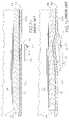
- the preferred mechanism for producing this scrubbing actionis described in connection with the construction and interconnection of a preferred membrane assembly 72 a as best depicted in FIGS. 6 and 7 a - 7 b.
- FIG. 6shows an enlarged view of the central region 80 a of the membrane assembly 72 a .
- the contacts 88are arranged in a-square-like pattern suitable for engagement with a square-like arrangement of pads.
- FIG. 7 awhich represents a sectional view taken along lines 7 a - 7 a in FIG. 6
- each contactcomprises a relatively thick rigid beam 90 at one end of which is formed a rigid contact bump 92 .
- the contact bumpincludes thereon a contacting portion 93 which comprises a nub of rhodium fused to the contact bump.
- each beamis formed in an overlapping connection with the end of a flexible conductive trace 76 a to form a joint therewith.
- This conductive trace in conjunction with a back-plane conductive layer 94effectively provides a controlled impedance data/signal line to the contact because its dimensions are established using a photolithographic process.
- the backplane layerpreferably includes openings therein to assist, for example, with gas venting during fabrication.
- the membrane assemblyis interconnected to the flat support surface 70 by an interposed elastomeric layer 98 , which layer is coextensive with the support surface and can be formed by a silicone rubber compound such as ELMER'S STICK-ALLTM made by the Borden Company or Sylgard 182 by Dow Corning Corporation. This compound can be conveniently applied in a paste-like phase which hardens as it sets.
- the flat support surfaceas previously mentioned, is made of incompressible material and is preferably a hard dielectric such as polysulfone or glass.
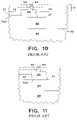
- FIG. 8shows, in dashed line view, the relative positions of the contact 88 and pad 100 at the moment of initial engagement or touchdown and, in solid-line view, these same elements after “overtravel” of the pad by a distance 106 in a vertical direction directly toward the flat support surface 70 .
- the distance 108 of lateral scrubbing movementis directly dependent on the vertical deflection of the contact 88 or, equivalently, on the overtravel distance 106 moved by the pad 100 .
- the elastomeric layer 98is backed by the incompressible support surface 70 , the elastomeric layer exerts a recovery force on each tilting beam 90 and thus each contact 93 to maintain contact-to-pad pressure during scrubbing. At the same time, the elastomeric layer accommodates some height variations between the respective contacts.
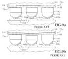
- FIG. 9 awhen a relatively shorter contact 88 a is situated between an immediately adjacent pair of relatively taller contacts 88 b and these taller contacts are brought into engagement with their respective pads, then, as indicated in FIG. 9 b , deformation by the elastomeric layer allows the smaller contact to be brought into engagement with its pad after some further overtravel by the pads.
- the tilting action of each contactis locally controlled, and the larger contacts are able, in particular, to tilt independently of the smaller contact so, that the smaller contact is not urged into lateral movement until it has actually touched down on its pad.
- the electroplating process to construct such a beam structureincludes the incompressible material 68 defining the support surface 70 and the substrate material attached thereon, such as the elastomeric layer 98 .
- the flexible conductive trace 76 ais then patterned on a sacrificial substrate.
- a polyimide layer 77is patterned to cover the entire surface of the sacrificial substrate and of the traces 76 a , except for the desired location of the beams 90 on a portion of the traces 76 a .
- the beams 90are then electroplated within the openings in the polyimide layer 77 .
- a layer of photoresist 79is patterned on both the surface of the polyimide 77 and beams 90 to leave openings for the desired location of the contact bumps 92 .
- the contact bumps 92are then electroplated within the openings in the photoresist layer 79 .
- the photoresist layer 79is removed and a thicker photoresist layer 81 is patterned to cover the exposed surfaces, except for the desired locations for the contacting portions 93 .
- the contacting portions 93are then electroplated within the openings in the photoresist layer 81 .
- the photoresist layer 81is then removed.
- the sacrificial substrate layeris removed and the remaining layers are attached to the elastomeric layer 98 .
- the resulting beams 90 , contact bumps 92 , and contacting portions 93provides the independent tilting and scrubbing functions of the device.
- the different heights of many of the beams 90 , contact bumps 92 , and contacting portions 93is compounded three fold in the overall height of many of the devices. Accordingly, many devices will have a significantly different height than other devices.
- Using membrane probes having variable device heightrequires more pressure to ensure that all the contacting portions 93 make adequate contact with the test device than would be required if all the devices had equal overall height.
- the cumulate effect of the additional pressure required for each devicemay exceed the total force permitted for the probe head and probe station. The excess pressure may also result in bending and breaking of the probe station, the probe head, and/or the membrane probing assembly.
- the devices with the greatest heightmay damage the pads on the test device because of the increased pressure required to make suitable contact for the devices with the lowest height.
- the ability to decrease the pitch (spacing) between the devicesis limited by the “mushrooming” effect of the electroplating process over the edges of the polyimide 77 and photoresist layers 79 and 81 .
- the “mushrooming” effectis difficult to control and results in a variable width of the beams 90 , contact bumps 92 , and contacting portions 93 . If the height of the beams 90 , the contact bumps 92 , or the contacting portions 93 are increased then the “mushrooming” effect generally increases, thus increasing the width of the respective portion. The increased width of one part generally results in a wider overall device which in turn increases the minimum spacing between contacting portions 93 .
- decreasing the height of the beams 90 , the contact bumps 92 , or the contacting portions 93generally decreases the width of the “mushrooming” effect which in turn decreases the minimum spacing between contacting portions 93 .
- the height of the contacting portions 93 relative to the respective beam 90is sufficiently reduced, then during use the rearward end of the beam 90 may sufficiently tilt and contact the test device in an acceptable location, i.e., off the contact pad.
- a second metal layerdirectly on top of a first metal layer, such as contacting portions 93 on the contact bumps 92 , especially when using nickel.
- an interface seed layersuch as copper or gold is used to make an improved interconnection.
- the interface seed layerreduces the lateral strength of the device due to the lower sheer strength of the interface layer.
- the photoresist layer 79 (and 81 ) over the raised portions of the beams 90tends to be thicker than the photoresist layer 79 (and 81 ) over the lower portions of the polyimide 77 .
- the thickness of the photoresist 79 (and 81 )tends to vary depending on the density of the beams 90 .
- the photoresist layer 79 (and 81 )will be thicker on average than regions of the membrane probe that have a less dense spacing of devices.
- the duration of the processdepends on the thickness of the photoresist 79 (or 81 ).
- variable photoresist thicknessit is difficult to properly process the photoresist to provide uniform openings.
- the thinner regions of photoresist layer 79 (or 81 )will tend to be overexposed resulting in variably sized openings.
- the greater the photoresist layer thickness 79 (or 81 )the greater the variability in its thickness. Accordingly, the use of photoresist presents many processing problems.
- the minimum size of the contacting portions 93is defined primarily by the lateral strength requirements and the maximum-allowable current density therein.
- the minimum size of the contacting portions 93accounting for the tolerances in alignment, in turn defines the minimum size of the contact bumps 92 so that the contacting portions 93 are definitely constructed on the contact bumps 92 .
- the minimum size of the contact bumps 92in view of the contacting portions 93 and accounting for the tolerances in alignment, defines the minimum size of the beams 90 so that the contact bumps 92 are definitely constructed on the beams 90 . Accordingly, the summation of the tolerances of the contact bumps 92 and the contacting portions 93 , together with a minimum size of the contacting portions 93 , defines the minimum device size, and thus defines the minimum pitch between contact pads.
- the present inventionovercomes the aforementioned drawbacks of the prior art by providing a substrate, preferably constructed of a ductile material.
- a tool having the desired shape of the resulting device for contacting contact pads on a test deviceis brought into contact with the substrate.
- the toolis preferably constructed of a material that is harder than the substrate so that a depression can be readily made therein.
- a dielectric (insulative) layer, that is preferably patterned,is supported by the substrate.
- a conductive materialis located within the depressions and then preferably planarized to remove excess from the top surface of the dielectric layer and to provide a flat overall surface.
- a traceis patterned on the dielectric layer and the conductive material.
- a polyimide layeris then preferably patterned over the entire surface. The substrate is then removed by any suitable process.
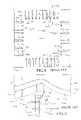
- FIG. 1is a perspective view of a membrane probing assembly bolted to a probe head and a wafer supported on a chuck in suitable position for probing by this assembly.
- FIG. 2is a bottom elevational view showing various parts of the probing assembly of FIG. 1 , including a support element and flexible membrane assembly, and a fragmentary view of a probe card having data/signal lines connected with corresponding lines on the membrane assembly.
- FIG. 3is a side elevational view of the membrane probing assembly of FIG. 1 where a portion of the membrane assembly has been cut away to expose hidden portions of the support element.
- FIG. 4is a top elevational view of an exemplary support element.
- FIGS. 5 a - 5 bare schematic side elevational views illustrating how the support element and membrane assembly are capable of tilting to match the orientation of the device under test.
- FIG. 6is an enlarged top elevational view of the central region of the construction of the membrane assembly of FIG. 2 .
- FIGS. 7 a - 7 bare sectional views taken along lines 7 a - 7 a in FIG. 6 first showing a contact before touchdown and then showing the same contact after touchdown and scrub movement across its respective pad.
- FIG. 8is a schematic side view showing, in dashed-line representation, the contact of FIGS. 7 a - 7 b at the moment of initial touchdown and, in solid-line representation, the same contact after further vertical overtravel by the pad.
- FIGS. 9 a and 9 billustrate the deformation of the elastomeric layer to bring the contacts into contact with its pad.
- FIG. 10is a longitudinal sectional view of the device of FIG. 8 .
- FIG. 11is a cross sectional view of the device of FIG. 8 .
- FIG. 12is a more accurate pictorial view of the device shown in FIGS. 10 and 11 .
- FIG. 13is a detailed view of the device shown in FIG. 11 illustrating the uneven layers that result during processing.
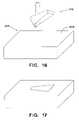
- FIG. 14is a pictorial view of a substrate.
- FIG. 15is a pictorial view of an exemplary embodiment of a tool, and in particular a dimpling tool, of the present invention.
- FIG. 16is a pictorial view illustrating the tool of FIG. 15 coming into contact with the substrate of FIG. 14 .
- FIG. 17is a pictorial view of the substrate of FIG. 14 after the tool of FIG. 15 has come into contact therewith.
- FIG. 18is a sectional view of the substrate of FIG. 14 with a polyimide layer supported thereon.
- FIG. 19is a pictorial view of the tool of FIG. 16 together with a z-axis stop.
- FIG. 20is a sectional view of the substrate of FIG. 14 with a trace, conductive material in the depression, and additional polyimide layer thereon.
- FIG. 21is a pictorial view of the device of FIG. 20 , inverted, with the substrate removed.
- FIG. 22is a breakaway sectional view of the contacting portion of FIG. 21 .
- FIG. 23is a schematic view illustrating one arrangement of the devices of the present invention.
- FIG. 24is a schematic view illustrating the contact of a traditional contacting portion and the oxide layer of a solder bump.
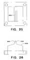
- FIG. 25is a plan view of an alternative device with an elongate probing portion.
- FIG. 26is a side view of the device of FIG. 25 with an elongate probing portion.
- FIG. 27is a pictorial view of a solder bump with a mark therein as a result of the device of FIGS. 25 and 26 .
- FIG. 28is a pictorial view of another alternative probing device.
- FIG. 29is a pictorial view of a further alternative probing device suitable for solder bumps.
- FIG. 30is a side view of a true Kelvin connection using the devices of the present invention.
- the currently employed construction techniques for membrane probesinvolves starting with the flat rigid substrate to support additional layers fabricated thereon. To decrease the pitch and provide devices with increased uniformity requires increasingly more complex and expensive processing techniques.
- the present inventorscame to the realization that by using a suitable tool a substrate may be coined to create the desired beams, contact bumps, and contacting portions. The remaining layers are then constructed “top down” on the beam. The substrate itself is thereafter removed.
- a substrate 200is preferably constructed from a ductile material such as aluminum, copper, lead, indium, brass, gold, silver, platinum, or tantalum, with a thickness preferably between 10 mills and 1 ⁇ 8 inch.
- the top surface 202 of the substrate 200is preferably planar and polished for optical clarity to improve-viewing, as described later.
- a tool and in particular a “dimpling” tool 210is constructed with a head 212 having the desired shape of the resulting device for contacting the contact pads on the test device.
- the dimpling tool 210includes a projection 214 to connect to a dimpling machine (not shown).
- the tool 210is supported by the dimpling machine with the head 212 oriented to come into contact with the top surface 202 of the substrate 200 .
- the tool 210is preferably constructed of a material that is harder than the substrate 200 so that a dimple can be readily made therein. Suitable material for the tool 210 is, for example, tool steel, carbide, chromium, and diamond.
- the preferred dimpling machineis a probe station which has accurate x, y, and z control.
- the tool 210is pressed into contact with the top surface 202 of the substrate 200 resulting in a depression 216 matching the shape of the tool 210 upon its removal from the substrate 200 , as shown in FIG. 17 .
- the tool 210is used to create a plurality of depressions 216 in the substrate 200 matching the desired pattern, such as the pattern shown in FIG. 6 .
- the tool 210can be held stationary and the substrate 200 can be moved in the z-direction until the top surface 202 of the substrate is pressed into contact with the tool 210 resulting in the same depression 216 matching the shape of the tool 210 upon its removal from the substrate 200 , as shown in FIG. 17 .
- a polyimide layer 220is patterned around the depressions 216 . It is to be understood that any other suitable insulative layer or dielectric layer may likewise be used. In the process of patterning the polyimide layer 220 , it is somewhat difficult to remove the polyimide from the depressions 216 during the exposing and etching process for the polyimide layer 220 . This is especially true when the depressions 216 are relatively deep with steeply inclined sides.
- the polyimide layer 220may be patterned on the top surface 202 of the substrate 200 with openings located therein where the depressions 216 are desired. Thereafter, the tool 210 is used to create the depressions 216 in the substrate 200 through the openings provided in the polyimide layer 220 . This alternative technique eliminates the difficult process of adequately removing the polyimide layer 220 from the depressions 216 .
- the tool 210in combination with the dimpling machine, can be aligned to the actual location of one of the openings that results from exposing and etching the polyimide layer 220 with a relatively inexpensive, and somewhat inaccurate mask.
- the present inventorscame to the realization that localized regions of the mask, and thus the openings resulting therefrom, tend to be relatively well aligned for purposes of dimpling. Likewise, regions of the mask distant from one another tend not to be relatively well aligned for purposes of dimpling.
- the present inventorscame to the realization that the dimpling machine may be realigned to the actual openings in the polyimide layer 220 at different remote locations, so that each localized region is relatively accurately aligned, while the overall alignment may be somewhat off. In this manner a relatively inexpensive mask may be used.
- the dimpling machineincludes accurate z-axis movement so that the depth of each depression is identical, or substantially identical.
- an alternative dimpling tool 240 with a built in z-axis stop 242may be used.
- the z-axis stop 242is a projection extending outward from the head 244 that comes to rest on the top surface of the polyimide 220 or top surface 202 of the substrate 200 .
- the z-axis stop 242is positioned with respect to the head 244 such that the proper depth is obtained, taking into account whether or not the polyimide layer 220 is previously patterned before using the dimpling tool 240 .
- a conductive material 250is electroplated onto the polyimide 220 and substrate 200 thereby filling up the depressions 216 with the conductive material 250 , such as nickel and rhodium. It is to be understood that any other suitable technique may be used to locate conductive material within the depressions 216 .
- the conductive material 250is then preferably lapped to remove excess from the top surface of the polyimide layer 220 and to provide a flat overall surface.
- the preferred lapping processis a chemical-mechanical planarization process.
- a trace 252is patterned on the polyimide layer 220 and the conductive material 250 .
- the trace 252is preferably a good conductor such as copper, aluminum, or gold.
- a polyimide layer 254is then patterned over the entire surface.
- the substrate 200is then removed by any suitable process, such as etching with hydrochloric acid (HCL 15%) or sulfuric acid (H 2 SO 4 ). Hydrochloric acid and sulfuric acid are not reactive with the polyimide layer 220 nor the conductive material 250 , such as nickel or rhodium. It is to be understood that the polyimide layer 254 may alternatively be any suitable insulator or dielectric layer.
- the contacting portion 260 of the resulting deviceis preferably selected to have a low contact resistance so that a good electrical connection may be made with the test device. While nickel has a relatively low contact resistance, rhodium has an even lower contact resistance and is more resistant to wear than nickel. Accordingly, the depressions 216 are preferably coated with a layer of rhodium. Using normal processing techniques the thickness of rhodium is limited to approximately 5 microns.
- the resulting deviceincludes an exterior layer of rhodium, and in particular the contacting portion 260 , which is then filled with the remaining conductive material, such as nickel or a nonconductive fill. The conductive material need not fill the entire depression.
- top-down construction processprovides numerous advantages over the traditional “bottom-up” processing technique of constructing layers upon a supporting substrate. These advantages also permit the capability of constructing devices with improved characteristics.
- the elevation of the contacting portions 260 of the devicesis extremely uniform because it is defined solely by the tooling process, which is mechanical in nature. Different localized current densities of the electroplating bath, different densities of the ions within the electroplating bath, and “random” variations in the electroplating bath are eliminated from impacting the overall shape and height of the resulting devices. With substantially uniform elevation of the devices, less force is required for the devices to make adequate contact with the test device which, in turn, decreases the likelihood of bending and breaking the probe station, the probe head, and/or the membrane probing assembly. Also, the substantially uniform elevation of the devices decreases the likelihood of damaging contact pads on the test device with excessive pressure.
- the contacting portion 260 of the devicesare stronger because the device is constructed of a single homogenous material during one depositing process requiring no interfacial layers, as previously required for the multiple processing steps. This permits reducing the size of the contacting portions to the limitation of the maximum current density allowable therein during testing and not the minimum sheer force of the interfacial layers.
- the shape of the resulting devicesare customizable to effectively probe different materials.
- the shape of the devicemay have steep sidewall angles, such as 85 degrees, while still providing mechanical strength, stability, and integrity.
- the steep sidewallspermit narrower devices to be constructed which allows or a greater density of devices for increasingly denser arrangements of contact pads on the test device.
- the angle of the sidewallsare not dependent (e.g. independent) on the crystalline structure of the substrate.
- the shape of the contacting portionis known precisely, and is uniform between devices, which permits uniform contact with the contact pads of the test device.
- the alignment of the different portions of the resulting deviceare exactly uniform between devices because each device was constructed using the same tooling process. With exact alignment of the lower portions of each device (beam and contact bump) in relation to the contacting portion, there is no need to provide additional leeway to accommodate processing variations inherent in photoresist processes and in electroplating processes. Also, the “mushrooming” effect of the electroplating process is eliminated which also reduces the required size of the device.
- the alignment variability reduction, and virtual elimination, of different devices 300allows a significantly decreased pitch to be obtained, suitable for contact pads on the test device that have increased density.
- the shape of the resulting devicesmay be tailor shaped to provide optimal mechanical performance.
- the deviceshould have a beam and bump structure that tilts upon contact.
- the device 300may include an inclined surface 304 between its tail 302 and the contacting portion 260 .
- the inclined surface 304provides for increased strength along portions of the length of the device 300 which permits the tail 302 to be thinner than its head 306 .
- the torque forces applied to the device 300 during the tilting process of the device 300tend to decrease over the length of the device 300 which has a correspondingly thinner material defined by the inclined surface 304 .
- With a thinner tail 302 and material proximate the tail 302the tail 302 of the device 300 has less likelihood of impacting the test device if excess tiling occurs.
- the improved shape of the device 300also decreases the amount of metal material required.
- “look-up” camerasare used to obtain an image of the lower portion of the membrane probe to determine the precise location of the devices 300 relative to the contact pads on the test device. Using “look-up” cameras permits automatic alignment of the membrane devices relative to the contact pads so that automatic testing may be performed. In order to obtain an image of the devices 300 on the membrane probe the “look-up” cameras normally utilize light to illuminate the devices 300 . Unfortunately, the traditional planar processing techniques result in relatively flat surfaces on the beams, contact bumps, and contacting portions, in a perpendicular orientation to the “look up” cameras each of which reflects light back to the “look-up” camera. The light reflecting back to the “look up” camera from all the surfaces frequently results in some confusion regarding the exact location of the contacting portions 260 .
- the inclined surface 304 of the devices 300tends to reflect incident light away from lowerly disposed “look-up” cameras, while the contacting portions 306 tend to reflect incident light back to lowerly disposed “look-up” cameras. Light returning to the “look-up” camera primarily from the contacting portions 306 results in less potential confusion regarding the exact location of the contacting portions.
- the initial polishing of the top surface 202 of the substrate 200results in a matching smooth lower surface for the polyimide layer 220 patterned thereon.
- the lower surface of the polyimide layer 220is smooth and the resulting polyimide layer 220 is generally optically clear.
- the spaces between the traces and the metallized devices 300is relatively optically transmissive so that an operator positioning the device can readily see through the device between the traces and devices. This assists the operator in manually positioning the membrane probe on the devices which are otherwise obscured.
- the pyramidal shape of the devices 300allows the operator to more easily determine the exact location of the contacting portions relative to the contact pads on the test device, which were previously obscured by the wide beam structures (relative to the contacting portions).
- the contacting portions 260 of the deviceare preferably constructed with an exterior surface of rhodium 340 , which typically can be effectively plated to only approximately a thickness of 5 microns.
- the plating process of rhodiumis semi-conformal, so the resulting layer is approximately 5 microns thick in a perpendicular direction to the exterior sides 352 and 354 .
- the width of the top 350 of the contacting portion and the angle of the sides 352 and 354 of the tool 210is selected so that the rhodium 340 plated on both sides 352 and 254 preferably join together forming a v-shape.
- the remainder of the deviceis preferably nickel.
- the thickness of the rhodium 340is only 5 microns in a perpendicular direction, the thickness of the rhodium 340 in a perpendicular direction from the top 350 of the device is greater than 5 microns. Accordingly, the contacting portion which wears during use in a generally perpendicular direction from the top 350 will last longer than if the top portion were merely plated to a thickness of 5 microns of rhodium.
- the texture of the contacting portion 260may be selected to provide the described scrubbing effect on the contact pads of the test device.
- the toolmay include a roughened surface pattern on the corresponding contacting portion to provide a uniform texture for all devices.
- the aforementioned construction techniquealso provides several advantages related to the shape of the devices which would be otherwise difficult, if not impossible, to construct.
- the toolmay provide any desired shape, such as a simple bump, if no scrubbing action is desired.
- the inclined supporting sides of the test device up to the contacting portion 260provides superior mechanical support for the contacting portion 260 , as opposed to merely a portion of metal supported by a larger contact bump.
- the contacting portionmay be smaller without risk of it becoming detached from the device.
- the smaller contacting portionprovides improved contact with the contact pad of the test device when the device tilts to penetrate the oxide buildup on the surface of the contact pad.
- the tail 302 of the devicemay be substantially thinner than the remainder of the device which decreases the likelihood of the tail 302 portion impacting the contact pad of the test device during testing when the device tilts.
- the pressure exerted by the contacting portions of the devicesis variable by changing the center of rotation of the device.
- the center of rotation of the devicecan be selected by selecting the length of the device and the location/height of the contacting portion relative thereto. Accordingly, the pressures can 35 be selected, as desired, to match characteristics of two different contact pads.
- a triangular shape of the footprint of the deviceallows for high lateral stability of the devices while permitting a decrease in the pitch between devices.
- the contacting portions 403 of the deviceare preferably aligned in a linear arrangement for many contact pads of test devices.
- the triangular portions of the deviceare aligned in alternatively opposing directions.
- the capability of constructing contacting portions that are raised high from the lower surface of the device, while still maintaining uniformity in the device height and structural strength,allows the device to provide scrubbing action while the lower surface of the device requires little movement.
- the small movement of the lower surface of the device to make good electrical contact during testingdecreases the stress on the layers under the lower surface of the device. Accordingly, the likelihood of cracking the polyimide layers and the conductive traces is reduced.
- the oxide layer developed thereonis difficult to effectively penetrate.
- the oxide 285tends to be pressed into the solder bump 287 together with the contacting portion 289 resulting in a poor interconnection.
- the needlestend to skate on the solder bumps, bend under within the solder bumps, collect debris on the needles, flake the debris onto the surface of the test device, and cleaning the needle probes is time consuming and tedious.
- FIGS. 25 and 26an improved device construction suitable for probing solder bumps is shown.
- the upper portion of the deviceincludes a pair of steeply inclined sides 291 and 293 , such as 15 degrees off vertical, with preferably polished sides.
- the inclined sides 291 and 293preferably form a sharp ridge 295 at the top thereof.
- the angle of the sides 291 and 293is selected with regard to the coefficient of friction between the sides and the oxide on the solder bump, so that the oxide coated surface tends to primarily slide along the surfaces of the sides 291 and 293 , or otherwise shear away, and not be significantly carried on the sides as the device penetrates a solder bump.
- the substantially sharp ridgealso provides for a mark (detent) after contact that extends across the entire solder bump. Subsequent heating of the solder bumps, together with flux, result in the flux exiting from the sides of the solder bump thereby avoiding the possibility of explosion.
- the resulting mark left on the solder bumpsis uniform in nature which allows manufacturers of the solder bumps to account for-the resulting marks in their design. Also, less force is required to be applied to the device because it tends to slice through the solder bump rather than make pressing contact with the solder bump. The flatter surface 405 prevents slicing too deeply into the solder ball (bump).
- a waffle patternmay be used.
- an alternative deviceincludes a pair of projections 311 and 313 that are preferably at the ends of an arch 315 .
- the spacing between the projections 311 and 313is preferably less than the diameter of the solder bump 317 to be tested. With such an arrangement the projections 311 and 313 will strike the sides of the solder bump 317 thereby not leaving a mark on the upper portion of the solder bump 317 . With marks on the sides of the solder bump 317 , the subsequent flux used will be less likely to become trapped within the mark and explode. In addition, if the alignment of the device is not centered on the solder bump 317 then it is highly likely that one of the projections 311 and 313 will still strike the solder bump 317 .
- Kelvin connectionsA more detailed analysis of Kelvin connections is described in Fink, D.G., ed., Electronics Engineers' Handbook, 1st ed., McGraw-Hill Book Co., 1975, Sec. 17-61, pp. 17-25, 17-26, “The Kelvin Double Bridge”, and U.S. patent application Ser. No. 08/864,287, both of which are incorporated by reference herein.
Landscapes
- Physics & Mathematics (AREA)
- General Physics & Mathematics (AREA)
- Engineering & Computer Science (AREA)
- Manufacturing & Machinery (AREA)
- Measuring Leads Or Probes (AREA)
- Testing Or Measuring Of Semiconductors Or The Like (AREA)
Abstract
Description
Claims (8)
Priority Applications (2)
| Application Number | Priority Date | Filing Date | Title |
|---|---|---|---|
| US10/772,172US7400155B2 (en) | 1998-07-14 | 2004-02-03 | Membrane probing system |
| US11/821,036US20070245536A1 (en) | 1998-07-14 | 2007-06-21 | Membrane probing system |
Applications Claiming Priority (3)
| Application Number | Priority Date | Filing Date | Title |
|---|---|---|---|
| US09/115,571US6256882B1 (en) | 1998-07-14 | 1998-07-14 | Membrane probing system |
| US09/814,594US6825677B2 (en) | 1998-07-14 | 2001-03-22 | Membrane probing system |
| US10/772,172US7400155B2 (en) | 1998-07-14 | 2004-02-03 | Membrane probing system |
Related Parent Applications (1)
| Application Number | Title | Priority Date | Filing Date |
|---|---|---|---|
| US09/814,594ContinuationUS6825677B2 (en) | 1998-07-14 | 2001-03-22 | Membrane probing system |
Related Child Applications (1)
| Application Number | Title | Priority Date | Filing Date |
|---|---|---|---|
| US11/821,036ContinuationUS20070245536A1 (en) | 1998-07-14 | 2007-06-21 | Membrane probing system |
Publications (2)
| Publication Number | Publication Date |
|---|---|
| US20040154155A1 US20040154155A1 (en) | 2004-08-12 |
| US7400155B2true US7400155B2 (en) | 2008-07-15 |
Family
ID=22362195
Family Applications (11)
| Application Number | Title | Priority Date | Filing Date |
|---|---|---|---|
| US09/115,571Expired - LifetimeUS6256882B1 (en) | 1998-07-14 | 1998-07-14 | Membrane probing system |
| US09/814,584Expired - Fee RelatedUS6860009B2 (en) | 1998-07-14 | 2001-03-22 | Probe construction using a recess |
| US09/814,594Expired - LifetimeUS6825677B2 (en) | 1998-07-14 | 2001-03-22 | Membrane probing system |
| US09/814,593Expired - Fee RelatedUS6708386B2 (en) | 1998-07-14 | 2001-03-22 | Method for probing an electrical device having a layer of oxide thereon |
| US10/705,014Expired - Fee RelatedUS7761986B2 (en) | 1998-07-14 | 2003-11-10 | Membrane probing method using improved contact |
| US10/772,172Expired - Fee RelatedUS7400155B2 (en) | 1998-07-14 | 2004-02-03 | Membrane probing system |
| US11/036,739Expired - Fee RelatedUS7266889B2 (en) | 1998-07-14 | 2005-01-14 | Membrane probing system |
| US11/821,036AbandonedUS20070245536A1 (en) | 1998-07-14 | 2007-06-21 | Membrane probing system |
| US11/888,429Expired - Fee RelatedUS7681312B2 (en) | 1998-07-14 | 2007-07-31 | Membrane probing system |
| US12/818,521Expired - Fee RelatedUS8451017B2 (en) | 1998-07-14 | 2010-06-18 | Membrane probing method using improved contact |
| US13/901,328AbandonedUS20130321018A1 (en) | 1998-07-14 | 2013-05-23 | Membrane probing method using improved contact |
Family Applications Before (5)
| Application Number | Title | Priority Date | Filing Date |
|---|---|---|---|
| US09/115,571Expired - LifetimeUS6256882B1 (en) | 1998-07-14 | 1998-07-14 | Membrane probing system |
| US09/814,584Expired - Fee RelatedUS6860009B2 (en) | 1998-07-14 | 2001-03-22 | Probe construction using a recess |
| US09/814,594Expired - LifetimeUS6825677B2 (en) | 1998-07-14 | 2001-03-22 | Membrane probing system |
| US09/814,593Expired - Fee RelatedUS6708386B2 (en) | 1998-07-14 | 2001-03-22 | Method for probing an electrical device having a layer of oxide thereon |
| US10/705,014Expired - Fee RelatedUS7761986B2 (en) | 1998-07-14 | 2003-11-10 | Membrane probing method using improved contact |
Family Applications After (5)
| Application Number | Title | Priority Date | Filing Date |
|---|---|---|---|
| US11/036,739Expired - Fee RelatedUS7266889B2 (en) | 1998-07-14 | 2005-01-14 | Membrane probing system |
| US11/821,036AbandonedUS20070245536A1 (en) | 1998-07-14 | 2007-06-21 | Membrane probing system |
| US11/888,429Expired - Fee RelatedUS7681312B2 (en) | 1998-07-14 | 2007-07-31 | Membrane probing system |
| US12/818,521Expired - Fee RelatedUS8451017B2 (en) | 1998-07-14 | 2010-06-18 | Membrane probing method using improved contact |
| US13/901,328AbandonedUS20130321018A1 (en) | 1998-07-14 | 2013-05-23 | Membrane probing method using improved contact |
Country Status (2)
| Country | Link |
|---|---|
| US (11) | US6256882B1 (en) |
| TW (1) | TW492219B (en) |
Cited By (7)
| Publication number | Priority date | Publication date | Assignee | Title |
|---|---|---|---|---|
| WO2010059247A3 (en)* | 2008-11-21 | 2011-03-24 | Cascade Microtech, Inc. | Replaceable coupon for a probing apparatus |
| US9435855B2 (en) | 2013-11-19 | 2016-09-06 | Teradyne, Inc. | Interconnect for transmitting signals between a device and a tester |
| US9594114B2 (en) | 2014-06-26 | 2017-03-14 | Teradyne, Inc. | Structure for transmitting signals in an application space between a device under test and test electronics |
| US9977052B2 (en) | 2016-10-04 | 2018-05-22 | Teradyne, Inc. | Test fixture |
| US10677815B2 (en) | 2018-06-08 | 2020-06-09 | Teradyne, Inc. | Test system having distributed resources |
| US11363746B2 (en) | 2019-09-06 | 2022-06-14 | Teradyne, Inc. | EMI shielding for a signal trace |
| US11862901B2 (en) | 2020-12-15 | 2024-01-02 | Teradyne, Inc. | Interposer |
Families Citing this family (89)
| Publication number | Priority date | Publication date | Assignee | Title |
|---|---|---|---|---|
| US5345170A (en) | 1992-06-11 | 1994-09-06 | Cascade Microtech, Inc. | Wafer probe station having integrated guarding, Kelvin connection and shielding systems |
| US6380751B2 (en) | 1992-06-11 | 2002-04-30 | Cascade Microtech, Inc. | Wafer probe station having environment control enclosure |
| US6232789B1 (en) | 1997-05-28 | 2001-05-15 | Cascade Microtech, Inc. | Probe holder for low current measurements |
| US5561377A (en) | 1995-04-14 | 1996-10-01 | Cascade Microtech, Inc. | System for evaluating probing networks |
| US5914613A (en)* | 1996-08-08 | 1999-06-22 | Cascade Microtech, Inc. | Membrane probing system with local contact scrub |
| US6002263A (en) | 1997-06-06 | 1999-12-14 | Cascade Microtech, Inc. | Probe station having inner and outer shielding |
| US6256882B1 (en)* | 1998-07-14 | 2001-07-10 | Cascade Microtech, Inc. | Membrane probing system |
| US6441315B1 (en)* | 1998-11-10 | 2002-08-27 | Formfactor, Inc. | Contact structures with blades having a wiping motion |
| US6578264B1 (en)* | 1999-06-04 | 2003-06-17 | Cascade Microtech, Inc. | Method for constructing a membrane probe using a depression |
| US7215131B1 (en)* | 1999-06-07 | 2007-05-08 | Formfactor, Inc. | Segmented contactor |
| US6445202B1 (en) | 1999-06-30 | 2002-09-03 | Cascade Microtech, Inc. | Probe station thermal chuck with shielding for capacitive current |
| US6759858B2 (en)* | 1999-10-20 | 2004-07-06 | Intel Corporation | Integrated circuit test probe having ridge contact |
| US6838890B2 (en)* | 2000-02-25 | 2005-01-04 | Cascade Microtech, Inc. | Membrane probing system |
| US6965226B2 (en) | 2000-09-05 | 2005-11-15 | Cascade Microtech, Inc. | Chuck for holding a device under test |
| US6914423B2 (en) | 2000-09-05 | 2005-07-05 | Cascade Microtech, Inc. | Probe station |
| DE20114544U1 (en) | 2000-12-04 | 2002-02-21 | Cascade Microtech, Inc., Beaverton, Oreg. | wafer probe |
| US6481098B1 (en)* | 2001-07-05 | 2002-11-19 | Shou-Chih Lin Chen | Method of manufacturing circuit boards |
| US20040169521A1 (en)* | 2001-08-02 | 2004-09-02 | Rincon Reynaldo M. | High density probe card apparatus and method of manufacture |
| US7355420B2 (en) | 2001-08-21 | 2008-04-08 | Cascade Microtech, Inc. | Membrane probing system |
| WO2003020467A1 (en) | 2001-08-31 | 2003-03-13 | Cascade Microtech, Inc. | Optical testing device |
| JP2003215161A (en)* | 2002-01-22 | 2003-07-30 | Tokyo Electron Ltd | Probe, method of manufacturing probe, method and device for attaching probe, and probe card |
| US6777964B2 (en) | 2002-01-25 | 2004-08-17 | Cascade Microtech, Inc. | Probe station |
| US7265565B2 (en) | 2003-02-04 | 2007-09-04 | Microfabrica Inc. | Cantilever microprobes for contacting electronic components and methods for making such probes |
| US20060053625A1 (en)* | 2002-05-07 | 2006-03-16 | Microfabrica Inc. | Microprobe tips and methods for making |
| US20060051948A1 (en)* | 2003-02-04 | 2006-03-09 | Microfabrica Inc. | Microprobe tips and methods for making |
| KR100864916B1 (en) | 2002-05-23 | 2008-10-22 | 캐스케이드 마이크로테크 인코포레이티드 | Probes for Testing Devices Under Test |
| US6847219B1 (en) | 2002-11-08 | 2005-01-25 | Cascade Microtech, Inc. | Probe station with low noise characteristics |
| US6724205B1 (en) | 2002-11-13 | 2004-04-20 | Cascade Microtech, Inc. | Probe for combined signals |
| US7250779B2 (en) | 2002-11-25 | 2007-07-31 | Cascade Microtech, Inc. | Probe station with low inductance path |
| US6920689B2 (en)* | 2002-12-06 | 2005-07-26 | Formfactor, Inc. | Method for making a socket to perform testing on integrated circuits |
| US6861856B2 (en) | 2002-12-13 | 2005-03-01 | Cascade Microtech, Inc. | Guarded tub enclosure |
| US20080211524A1 (en)* | 2003-02-04 | 2008-09-04 | Microfabrica Inc. | Electrochemically Fabricated Microprobes |
| US20080157793A1 (en)* | 2003-02-04 | 2008-07-03 | Microfabrica Inc. | Vertical Microprobes for Contacting Electronic Components and Method for Making Such Probes |
| US10416192B2 (en) | 2003-02-04 | 2019-09-17 | Microfabrica Inc. | Cantilever microprobes for contacting electronic components |
| US7221172B2 (en) | 2003-05-06 | 2007-05-22 | Cascade Microtech, Inc. | Switched suspended conductor and connection |
| US7057404B2 (en) | 2003-05-23 | 2006-06-06 | Sharp Laboratories Of America, Inc. | Shielded probe for testing a device under test |
| US7492172B2 (en) | 2003-05-23 | 2009-02-17 | Cascade Microtech, Inc. | Chuck for holding a device under test |
| US7319341B1 (en)* | 2003-08-28 | 2008-01-15 | Altera Corporation | Method of maintaining signal integrity across a capacitive coupled solder bump |
| JP4199629B2 (en)* | 2003-09-18 | 2008-12-17 | 株式会社日立ハイテクノロジーズ | Internal structure observation method and apparatus |
| US7250626B2 (en) | 2003-10-22 | 2007-07-31 | Cascade Microtech, Inc. | Probe testing structure |
| WO2005065258A2 (en) | 2003-12-24 | 2005-07-21 | Cascade Microtech, Inc. | Active wafer probe |
| US7187188B2 (en) | 2003-12-24 | 2007-03-06 | Cascade Microtech, Inc. | Chuck with integrated wafer support |
| US20080108221A1 (en)* | 2003-12-31 | 2008-05-08 | Microfabrica Inc. | Microprobe Tips and Methods for Making |
| WO2005121824A2 (en) | 2004-06-07 | 2005-12-22 | Cascade Microtech, Inc. | Thermal optical chuck |
| US7330041B2 (en) | 2004-06-14 | 2008-02-12 | Cascade Microtech, Inc. | Localizing a temperature of a device for testing |
| KR101157449B1 (en) | 2004-07-07 | 2012-06-22 | 캐스케이드 마이크로테크 인코포레이티드 | Probe head having a membrane suspended probe |
| US8114172B2 (en)* | 2004-07-30 | 2012-02-14 | Extreme Reality Ltd. | System and method for 3D space-dimension based image processing |
| EP1789812A2 (en) | 2004-09-13 | 2007-05-30 | Cascade Microtech, Inc. | Double sided probing structures |
| US7119562B2 (en)* | 2005-01-10 | 2006-10-10 | Wintek Corporation | Contact-type film probe |
| US7656172B2 (en) | 2005-01-31 | 2010-02-02 | Cascade Microtech, Inc. | System for testing semiconductors |
| US7535247B2 (en) | 2005-01-31 | 2009-05-19 | Cascade Microtech, Inc. | Interface for testing semiconductors |
| US7449899B2 (en) | 2005-06-08 | 2008-11-11 | Cascade Microtech, Inc. | Probe for high frequency signals |
| JP5080459B2 (en) | 2005-06-13 | 2012-11-21 | カスケード マイクロテック インコーポレイテッド | Wideband active / passive differential signal probe |
| JP4884749B2 (en)* | 2005-10-31 | 2012-02-29 | 日本発條株式会社 | Manufacturing method of conductive contact holder and manufacturing method of conductive contact unit |
| DE102006002753B4 (en)* | 2006-01-20 | 2010-09-30 | X-Fab Semiconductor Foundries Ag | Method and apparatus for evaluating the undercut of deep trench structures in SOI slices |
| US7609077B2 (en) | 2006-06-09 | 2009-10-27 | Cascade Microtech, Inc. | Differential signal probe with integral balun |
| US7403028B2 (en) | 2006-06-12 | 2008-07-22 | Cascade Microtech, Inc. | Test structure and probe for differential signals |
| US7443186B2 (en) | 2006-06-12 | 2008-10-28 | Cascade Microtech, Inc. | On-wafer test structures for differential signals |
| US7723999B2 (en) | 2006-06-12 | 2010-05-25 | Cascade Microtech, Inc. | Calibration structures for differential signal probing |
| US7764072B2 (en) | 2006-06-12 | 2010-07-27 | Cascade Microtech, Inc. | Differential signal probing system |
| US7498824B2 (en)* | 2006-08-22 | 2009-03-03 | Formfactor, Inc. | Method and apparatus for making a determination relating to resistance of probes |
| US7876114B2 (en) | 2007-08-08 | 2011-01-25 | Cascade Microtech, Inc. | Differential waveguide probe |
| US7888957B2 (en) | 2008-10-06 | 2011-02-15 | Cascade Microtech, Inc. | Probing apparatus with impedance optimized interface |
| US8319503B2 (en) | 2008-11-24 | 2012-11-27 | Cascade Microtech, Inc. | Test apparatus for measuring a characteristic of a device under test |
| US8115504B2 (en)* | 2008-12-08 | 2012-02-14 | Formfactor, Inc. | Microspring array having reduced pitch contact elements |
| JP5379065B2 (en)* | 2010-04-21 | 2013-12-25 | 新光電気工業株式会社 | Probe card and manufacturing method thereof |
| US8823406B2 (en) | 2010-10-20 | 2014-09-02 | Cascade Micotech, Inc. | Systems and methods for simultaneous optical testing of a plurality of devices under test |
| US8970240B2 (en) | 2010-11-04 | 2015-03-03 | Cascade Microtech, Inc. | Resilient electrical interposers, systems that include the interposers, and methods for using and forming the same |
| US9244099B2 (en) | 2011-05-09 | 2016-01-26 | Cascade Microtech, Inc. | Probe head assemblies, components thereof, test systems including the same, and methods of operating the same |
| JP5998378B2 (en)* | 2012-11-30 | 2016-09-28 | テクトロニクス・インコーポレイテッドTektronix,Inc. | Probing tips for signal acquisition probes |
| US9063172B1 (en) | 2013-05-16 | 2015-06-23 | M/A-Com Technology Solutions Holdings, Inc. | Step connectors in test fixture for packaged device measurement |
| US9678108B1 (en)* | 2014-02-06 | 2017-06-13 | Advantest America, Inc. | Methods to manufacture semiconductor probe tips |
| TWI586967B (en)* | 2015-10-27 | 2017-06-11 | Mpi Corp | Probe module |
| US10509071B2 (en)* | 2016-11-18 | 2019-12-17 | Taiwan Semiconductor Manufacturing Co., Ltd. | Method and system for aligning probe card in semiconductor device testing |
| CN111630648B (en)* | 2018-02-06 | 2023-12-29 | 株式会社日立高新技术 | Probe module and probe |
| US11973301B2 (en) | 2018-09-26 | 2024-04-30 | Microfabrica Inc. | Probes having improved mechanical and/or electrical properties for making contact between electronic circuit elements and methods for making |
| US11262383B1 (en) | 2018-09-26 | 2022-03-01 | Microfabrica Inc. | Probes having improved mechanical and/or electrical properties for making contact between electronic circuit elements and methods for making |
| US12181493B2 (en) | 2018-10-26 | 2024-12-31 | Microfabrica Inc. | Compliant probes including dual independently operable probe contact elements including at least one flat extension spring, methods for making, and methods for using |
| US12078657B2 (en) | 2019-12-31 | 2024-09-03 | Microfabrica Inc. | Compliant pin probes with extension springs, methods for making, and methods for using |
| CN109781788B (en)* | 2019-01-30 | 2021-02-26 | 南通大学 | A Nanoscale Insulating Thin Film Voltage-Current Characteristic Measurement System |
| US12000865B2 (en) | 2019-02-14 | 2024-06-04 | Microfabrica Inc. | Multi-beam vertical probes with independent arms formed of a high conductivity metal for enhancing current carrying capacity and methods for making such probes |
| US12196781B2 (en) | 2019-12-31 | 2025-01-14 | Microfabrica Inc. | Probes with planar unbiased spring elements for electronic component contact, methods for making such probes, and methods for using such probes |
| US11761982B1 (en) | 2019-12-31 | 2023-09-19 | Microfabrica Inc. | Probes with planar unbiased spring elements for electronic component contact and methods for making such probes |
| US11802891B1 (en) | 2019-12-31 | 2023-10-31 | Microfabrica Inc. | Compliant pin probes with multiple spring segments and compression spring deflection stabilization structures, methods for making, and methods for using |
| US12196782B2 (en) | 2019-12-31 | 2025-01-14 | Microfabrica Inc. | Probes with planar unbiased spring elements for electronic component contact, methods for making such probes, and methods for using such probes |
| US11774467B1 (en) | 2020-09-01 | 2023-10-03 | Microfabrica Inc. | Method of in situ modulation of structural material properties and/or template shape |
| US12146898B2 (en) | 2020-10-02 | 2024-11-19 | Microfabrica Inc. | Multi-beam probes with decoupled structural and current carrying beams and methods of making |
| US12306243B2 (en) | 2023-06-12 | 2025-05-20 | Formfactor, Inc. | Space transformers configured to be utilized in a probe system, probe systems that include the space transformers, and related methods |
| US12379395B2 (en)* | 2023-07-13 | 2025-08-05 | Formfactor, Inc. | Probes, probe blades, tools for probe blades, blade holders, and probe systems for electrically testing a device under test |
Citations (377)
| Publication number | Priority date | Publication date | Assignee | Title |
|---|---|---|---|---|
| US2389668A (en) | 1943-03-04 | 1945-11-27 | Barnes Drill Co | Indexing mechanism for machine tables |
| US3401126A (en) | 1965-06-18 | 1968-09-10 | Ibm | Method of rendering noble metal conductive composition non-wettable by solder |
| US3429040A (en) | 1965-06-18 | 1969-02-25 | Ibm | Method of joining a component to a substrate |
| US3445770A (en) | 1965-12-27 | 1969-05-20 | Philco Ford Corp | Microelectronic test probe with defect marker access |
| US3541222A (en) | 1969-01-13 | 1970-11-17 | Bunker Ramo | Connector screen for interconnecting adjacent surfaces of laminar circuits and method of making |
| US3596228A (en) | 1969-05-29 | 1971-07-27 | Ibm | Fluid actuated contactor |
| US3634807A (en) | 1969-03-28 | 1972-01-11 | Siemens Ag | Detachable electrical contact arrangement |
| US3654585A (en) | 1970-03-11 | 1972-04-04 | Brooks Research And Mfg Inc | Coordinate conversion for the testing of printed circuit boards |
| US3680037A (en) | 1970-11-05 | 1972-07-25 | Tech Wire Prod Inc | Electrical interconnector |
| US3700998A (en) | 1970-08-20 | 1972-10-24 | Computer Test Corp | Sample and hold circuit with switching isolation |
| US3806801A (en) | 1972-12-26 | 1974-04-23 | Ibm | Probe contactor having buckling beam probes |
| US3829076A (en) | 1972-06-08 | 1974-08-13 | H Sofy | Dial index machine |
| US3839672A (en) | 1973-02-05 | 1974-10-01 | Belden Corp | Method and apparatus for measuring the effectiveness of the shield in a coaxial cable |
| US3839627A (en) | 1973-12-03 | 1974-10-01 | Bacharach Instr Co | Multi-mode digital control apparatus |
| US3849728A (en) | 1973-08-21 | 1974-11-19 | Wentworth Labor Inc | Fixed point probe card and an assembly and repair fixture therefor |
| US3862790A (en) | 1971-07-22 | 1975-01-28 | Plessey Handel Investment Ag | Electrical interconnectors and connector assemblies |
| US3936743A (en) | 1974-03-05 | 1976-02-03 | Electroglas, Inc. | High speed precision chuck assembly |
| US3971610A (en) | 1974-05-10 | 1976-07-27 | Technical Wire Products, Inc. | Conductive elastomeric contacts and connectors |
| US4008900A (en) | 1976-03-15 | 1977-02-22 | John Freedom | Indexing chuck |
| US4027935A (en) | 1976-06-21 | 1977-06-07 | International Business Machines Corporation | Contact for an electrical contactor assembly |
| US4038599A (en) | 1974-12-30 | 1977-07-26 | International Business Machines Corporation | High density wafer contacting and test system |
| US4038894A (en) | 1975-07-18 | 1977-08-02 | Springfield Tool And Die, Inc. | Piercing apparatus |
| US4049252A (en) | 1976-02-04 | 1977-09-20 | Bell Theodore F | Index table |
| US4184729A (en) | 1977-10-13 | 1980-01-22 | Bunker Ramo Corporation | Flexible connector cable |
| US4284033A (en) | 1979-10-31 | 1981-08-18 | Rca Corporation | Means to orbit and rotate target wafers supported on planet member |
| US4312117A (en) | 1977-09-01 | 1982-01-26 | Raytheon Company | Integrated test and assembly device |
| US4531474A (en) | 1983-06-04 | 1985-07-30 | Dainippon Screen Manufacturing Co., Ltd. | Rotary board treating apparatus |
| US4581679A (en) | 1983-05-31 | 1986-04-08 | Trw Inc. | Multi-element circuit construction |
| US4593243A (en) | 1984-08-29 | 1986-06-03 | Magnavox Government And Industrial Electronics Company | Coplanar and stripline probe card apparatus |
| US4636722A (en) | 1984-05-21 | 1987-01-13 | Probe-Rite, Inc. | High density probe-head with isolated and shielded transmission lines |
| US4636772A (en) | 1985-01-17 | 1987-01-13 | Riken Denshi Co. Ltd. | Multiple function type D/A converter |
| US4649339A (en) | 1984-04-25 | 1987-03-10 | Honeywell Inc. | Integrated circuit interface |
| US4663840A (en) | 1984-12-11 | 1987-05-12 | U.S. Philips Corporation | Method of interconnecting conductors of different layers of a multilayer printed circuit board |
| US4673839A (en) | 1986-09-08 | 1987-06-16 | Tektronix, Inc. | Piezoelectric pressure sensing apparatus for integrated circuit testing stations |
| EP0230348A2 (en) | 1986-01-07 | 1987-07-29 | Hewlett-Packard Company | Test probe |
| US4697143A (en) | 1984-04-30 | 1987-09-29 | Cascade Microtech, Inc. | Wafer probe |
| JPS62239050A (en) | 1986-04-10 | 1987-10-19 | Kobe Steel Ltd | Eddy current test equipment |
| US4707657A (en) | 1984-06-13 | 1987-11-17 | Boegh Petersen Allan | Connector assembly for a circuit board testing machine, a circuit board testing machine, and a method of testing a circuit board by means of a circuit board testing machine |
| US4727319A (en) | 1985-12-24 | 1988-02-23 | Hughes Aircraft Company | Apparatus for on-wafer testing of electrical circuits |
| US4749942A (en) | 1985-09-26 | 1988-06-07 | Tektronix, Inc. | Wafer probe head |
| US4755746A (en) | 1985-04-24 | 1988-07-05 | Prometrix Corporation | Apparatus and methods for semiconductor wafer testing |
| US4791363A (en) | 1987-09-28 | 1988-12-13 | Logan John K | Ceramic microstrip probe blade |
| US4793814A (en) | 1986-07-21 | 1988-12-27 | Rogers Corporation | Electrical circuit board interconnect |
| US4795962A (en) | 1986-09-04 | 1989-01-03 | Hewlett-Packard Company | Floating driver circuit and a device for measuring impedances of electrical components |
| EP0304868A2 (en) | 1987-08-28 | 1989-03-01 | Tektronix Inc. | Multiple lead probe for integrated circuits in wafer form |
| US4827211A (en) | 1987-01-30 | 1989-05-02 | Cascade Microtech, Inc. | Wafer probe |
| US4837507A (en) | 1984-06-08 | 1989-06-06 | American Telephone And Telegraph Company At&T Technologies, Inc. | High frequency in-circuit test fixture |
| EP0259163A3 (en) | 1986-09-05 | 1989-07-12 | Tektronix, Inc. | Semiconductor wafer probe |
| US4849689A (en) | 1988-11-04 | 1989-07-18 | Cascade Microtech, Inc. | Microwave wafer probe having replaceable probe tip |
| US4871964A (en) | 1988-04-12 | 1989-10-03 | G. G. B. Industries, Inc. | Integrated circuit probing apparatus |
| US4894612A (en) | 1987-08-13 | 1990-01-16 | Hypres, Incorporated | Soft probe for providing high speed on-wafer connections to a circuit |
| US4899998A (en) | 1987-11-10 | 1990-02-13 | Hiroshi Teramachi | Rotational positioning device |
| US4904933A (en) | 1986-09-08 | 1990-02-27 | Tektronix, Inc. | Integrated circuit probe station |
| US4906920A (en) | 1988-10-11 | 1990-03-06 | Hewlett-Packard Company | Self-leveling membrane probe |
| US4912399A (en) | 1987-06-09 | 1990-03-27 | Tektronix, Inc. | Multiple lead probe for integrated circuits in wafer form |
| US4916002A (en) | 1989-01-13 | 1990-04-10 | The Board Of Trustees Of The Leland Jr. University | Microcasting of microminiature tips |
| US4918383A (en) | 1987-01-20 | 1990-04-17 | Huff Richard E | Membrane probe with automatic contact scrub action |
| US4922192A (en) | 1988-09-06 | 1990-05-01 | Unisys Corporation | Elastic membrane probe |
| JPH02129393A (en) | 1988-11-07 | 1990-05-17 | Fujitsu Ltd | Manufacturing method of semiconductor device |
| US4975638A (en) | 1989-12-18 | 1990-12-04 | Wentworth Laboratories | Test probe assembly for testing integrated circuit devices |
| US4980637A (en) | 1988-03-01 | 1990-12-25 | Hewlett-Packard Company | Force delivery system for improved precision membrane probe |
| US4983910A (en) | 1988-05-20 | 1991-01-08 | Stanford University | Millimeter-wave active probe |
| US4987100A (en) | 1988-05-26 | 1991-01-22 | International Business Machines Corporation | Flexible carrier for an electronic device |
| US4991290A (en) | 1988-07-21 | 1991-02-12 | Microelectronics And Computer Technology | Flexible electrical interconnect and method of making |
| US4998062A (en) | 1988-10-25 | 1991-03-05 | Tokyo Electron Limited | Probe device having micro-strip line structure |
| US5003253A (en) | 1988-05-20 | 1991-03-26 | The Board Of Trustees Of The Leland Stanford Junior University | Millimeter-wave active probe system |
| US5021186A (en) | 1988-03-25 | 1991-06-04 | Nissan Chemical Industries, Ltd. | Chloroisocyanuric acid composition having storage stability |
| US5020219A (en) | 1988-05-16 | 1991-06-04 | Leedy Glenn J | Method of making a flexible tester surface for testing integrated circuits |
| US5045781A (en) | 1989-06-08 | 1991-09-03 | Cascade Microtech, Inc. | High-frequency active probe having replaceable contact needles |
| US5059898A (en) | 1990-08-09 | 1991-10-22 | Tektronix, Inc. | Wafer probe with transparent loading member |
| US5061192A (en) | 1990-12-17 | 1991-10-29 | International Business Machines Corporation | High density connector |
| US5069628A (en) | 1990-03-13 | 1991-12-03 | Hughes Aircraft Company | Flexible electrical cable connector with double sided dots |
| US5097101A (en) | 1991-02-05 | 1992-03-17 | Tektronix, Inc. | Method of forming a conductive contact bump on a flexible substrate and a flexible substrate |
| JPH04165361A (en) | 1990-10-30 | 1992-06-11 | Toshiba Corp | Semiconductor processing method |
| US5126286A (en) | 1990-10-05 | 1992-06-30 | Micron Technology, Inc. | Method of manufacturing edge connected semiconductor die |
| US5134365A (en) | 1989-07-11 | 1992-07-28 | Nihon Denshizairyo Kabushiki Kaisha | Probe card in which contact pressure and relative position of each probe end are correctly maintained |
| US5133119A (en) | 1991-02-28 | 1992-07-28 | Hewlett-Packard Company | Shearing stress interconnection apparatus and method |
| US5136237A (en) | 1991-01-29 | 1992-08-04 | Tektronix, Inc. | Double insulated floating high voltage test probe |
| US5145552A (en) | 1989-12-21 | 1992-09-08 | Canon Kabushiki Kaisha | Process for preparing electrical connecting member |
| US5148103A (en) | 1990-10-31 | 1992-09-15 | Hughes Aircraft Company | Apparatus for testing integrated circuits |
| US5172050A (en) | 1991-02-15 | 1992-12-15 | Motorola, Inc. | Micromachined semiconductor probe card |
| US5177438A (en) | 1991-08-02 | 1993-01-05 | Motorola, Inc. | Low resistance probe for semiconductor |
| US5180977A (en) | 1991-12-02 | 1993-01-19 | Hoya Corporation Usa | Membrane probe contact bump compliancy system |
| DE4223658A1 (en) | 1991-07-18 | 1993-01-21 | Gold Star Electronics | Test appts. for semiconductor chips with relatively many connectors - uses tape automated bonding band with adhesive surface for connecting lines to test card and dendritically grown metal test points |
| US5207585A (en) | 1990-10-31 | 1993-05-04 | International Business Machines Corporation | Thin interface pellicle for dense arrays of electrical interconnects |
| US5225037A (en) | 1991-06-04 | 1993-07-06 | Texas Instruments Incorporated | Method for fabrication of probe card for testing of semiconductor devices |
| US5274336A (en) | 1992-01-14 | 1993-12-28 | Hewlett-Packard Company | Capacitively-coupled test probe |
| US5293175A (en) | 1991-07-19 | 1994-03-08 | Conifer Corporation | Stacked dual dipole MMDS feed |
| US5321352A (en) | 1991-08-01 | 1994-06-14 | Tokyo Electron Yamanashi Limited | Probe apparatus and method of alignment for the same |
| US5326412A (en) | 1992-12-22 | 1994-07-05 | Hughes Aircraft Company | Method for electrodepositing corrosion barrier on isolated circuitry |
| US5355079A (en) | 1993-01-07 | 1994-10-11 | Wentworth Laboratories, Inc. | Probe assembly for testing integrated circuit devices |
| US5367165A (en) | 1992-01-17 | 1994-11-22 | Olympus Optical Co., Ltd. | Cantilever chip for scanning probe microscope |
| US5371654A (en) | 1992-10-19 | 1994-12-06 | International Business Machines Corporation | Three dimensional high performance interconnection package |
| US5389885A (en) | 1992-01-27 | 1995-02-14 | Everett Charles Technologies, Inc. | Expandable diaphragm test modules and connectors |
| US5395253A (en) | 1993-04-29 | 1995-03-07 | Hughes Aircraft Company | Membrane connector with stretch induced micro scrub |
| US5412866A (en) | 1993-07-01 | 1995-05-09 | Hughes Aircraft Company | Method of making a cast elastomer/membrane test probe assembly |
| US5441690A (en) | 1993-07-06 | 1995-08-15 | International Business Machines Corporation | Process of making pinless connector |
| US5453404A (en) | 1992-10-13 | 1995-09-26 | Leedy; Glenn | Method for making an interconnection structure for integrated circuits |
| US5476211A (en) | 1993-11-16 | 1995-12-19 | Form Factor, Inc. | Method of manufacturing electrical contacts, using a sacrificial member |
| US5479108A (en) | 1992-11-25 | 1995-12-26 | David Cheng | Method and apparatus for handling wafers |
| US5481936A (en) | 1993-06-29 | 1996-01-09 | Yugen Kaisha Sozoan | Rotary drive positioning system for an indexing table |
| US5487999A (en) | 1991-06-04 | 1996-01-30 | Micron Technology, Inc. | Method for fabricating a penetration limited contact having a rough textured surface |
| US5506515A (en) | 1994-07-20 | 1996-04-09 | Cascade Microtech, Inc. | High-frequency probe tip assembly |
| US5517126A (en) | 1993-03-18 | 1996-05-14 | Tokyo Electron Limited | Probe apparatus |
| US5521518A (en) | 1990-09-20 | 1996-05-28 | Higgins; H. Dan | Probe card apparatus |
| US5532608A (en) | 1995-04-06 | 1996-07-02 | International Business Machines Corporation | Ceramic probe card and method for reducing leakage current |
| US5537372A (en) | 1991-11-15 | 1996-07-16 | International Business Machines Corporation | High density data storage system with topographic contact sensor |
| US5565788A (en) | 1994-07-20 | 1996-10-15 | Cascade Microtech, Inc. | Coaxial wafer probe with tip shielding |
| US5571324A (en) | 1993-07-26 | 1996-11-05 | Tokyo Ohka Kogyo Co., Ltd. | Rotary-cup coating apparatus |
| US5584120A (en)* | 1992-02-14 | 1996-12-17 | Research Organization For Circuit Knowledge | Method of manufacturing printed circuits |
| US5589781A (en) | 1990-09-20 | 1996-12-31 | Higgins; H. Dan | Die carrier apparatus |
| US5601740A (en) | 1993-11-16 | 1997-02-11 | Formfactor, Inc. | Method and apparatus for wirebonding, for severing bond wires, and for forming balls on the ends of bond wires |
| US5623214A (en) | 1994-10-14 | 1997-04-22 | Hughes Aircraft Company | Multiport membrane probe for full-wafer testing |
| US5623213A (en) | 1994-09-09 | 1997-04-22 | Micromodule Systems | Membrane probing of circuits |
| US5669316A (en) | 1993-12-10 | 1997-09-23 | Sony Corporation | Turntable for rotating a wafer carrier |
| US5676360A (en) | 1995-07-11 | 1997-10-14 | Boucher; John N. | Machine tool rotary table locking apparatus |
| US5686317A (en) | 1991-06-04 | 1997-11-11 | Micron Technology, Inc. | Method for forming an interconnect having a penetration limited contact structure for establishing a temporary electrical connection with a semiconductor die |
| US5685232A (en) | 1993-10-19 | 1997-11-11 | Canon Kabushiki Kaisha | Positioning stage device exposure apparatus and device manufacturing method utilizing the same |
| US5700844A (en) | 1996-04-09 | 1997-12-23 | International Business Machines Corporation | Process for making a foamed polymer |
| WO1998007040A1 (en) | 1996-08-08 | 1998-02-19 | Cascade Microtech, Inc. | Membrane probing system with local contact scrub |
| US5720098A (en) | 1995-05-12 | 1998-02-24 | Probe Technology | Method for making a probe preserving a uniform stress distribution under deflection |
| US5723347A (en) | 1993-09-30 | 1998-03-03 | International Business Machines Corp. | Semi-conductor chip test probe and process for manufacturing the probe |
| US5726211A (en) | 1996-03-21 | 1998-03-10 | International Business Machines Corporation | Process for making a foamed elastometric polymer |
| US5742174A (en) | 1995-11-03 | 1998-04-21 | Probe Technology | Membrane for holding a probe tip in proper location |
| US5756021A (en) | 1994-12-20 | 1998-05-26 | International Business Machines Corporation | Electronic devices comprising dielectric foamed polymers |
| US5772451A (en) | 1993-11-16 | 1998-06-30 | Form Factor, Inc. | Sockets for electronic components and methods of connecting to electronic components |
| US5785538A (en) | 1995-11-27 | 1998-07-28 | International Business Machines Corporation | High density test probe with rigid surface structure |
| US5804607A (en) | 1996-03-21 | 1998-09-08 | International Business Machines Corporation | Process for making a foamed elastomeric polymer |
| US5806181A (en) | 1993-11-16 | 1998-09-15 | Formfactor, Inc. | Contact carriers (tiles) for populating larger substrates with spring contacts |
| US5811982A (en) | 1995-11-27 | 1998-09-22 | International Business Machines Corporation | High density cantilevered probe for electronic devices |
| US5811751A (en) | 1994-02-18 | 1998-09-22 | New Wave Research | Multi-wavelength laser system, probe station and laser cutter system using the same |
| US5810607A (en) | 1995-09-13 | 1998-09-22 | International Business Machines Corporation | Interconnector with contact pads having enhanced durability |
| US5814847A (en) | 1996-02-02 | 1998-09-29 | National Semiconductor Corp. | General purpose assembly programmable multi-chip package substrate |
| US5813847A (en) | 1995-10-02 | 1998-09-29 | Abb Research Ltd. | Device and method for injecting fuels into compressed gaseous media |
| US5820014A (en) | 1993-11-16 | 1998-10-13 | Form Factor, Inc. | Solder preforms |
| US5829128A (en) | 1993-11-16 | 1998-11-03 | Formfactor, Inc. | Method of mounting resilient contact structures to semiconductor devices |
| US5832601A (en) | 1993-11-16 | 1998-11-10 | Form Factor, Inc. | Method of making temporary connections between electronic components |
| US5838160A (en) | 1994-04-07 | 1998-11-17 | International Business Machines Corporation | Integral rigid chip test probe |
| JPH114001A (en) | 1997-06-11 | 1999-01-06 | Semiconductor Energy Lab Co Ltd | Semiconductor device and manufacture thereof |
| US5869974A (en) | 1996-04-01 | 1999-02-09 | Micron Technology, Inc. | Micromachined probe card having compliant contact members for testing semiconductor wafers |
| US5876082A (en) | 1996-02-15 | 1999-03-02 | Singulus Technologies Gmbh | Device for gripping and holding substrates |
| US5878486A (en) | 1993-11-16 | 1999-03-09 | Formfactor, Inc. | Method of burning-in semiconductor devices |
| US5883522A (en) | 1996-11-07 | 1999-03-16 | National Semiconductor Corporation | Apparatus and method for retaining a semiconductor wafer during testing |
| US5896038A (en) | 1996-11-08 | 1999-04-20 | W. L. Gore & Associates, Inc. | Method of wafer level burn-in |
| US5900738A (en) | 1993-11-16 | 1999-05-04 | Formfactor, Inc. | Contact structure device for interconnections, interposer, semiconductor assembly and package using the same and method |
| US5912046A (en) | 1993-11-16 | 1999-06-15 | Form Factor, Inc. | Method and apparatus for applying a layer of flowable coating material to a surface of an electronic component |
| US5914614A (en) | 1996-03-12 | 1999-06-22 | International Business Machines Corporation | High density cantilevered probe for electronic devices |
| US5926029A (en) | 1997-05-27 | 1999-07-20 | International Business Machines Corporation | Ultra fine probe contacts |
| US5959461A (en) | 1997-07-14 | 1999-09-28 | Wentworth Laboratories, Inc. | Probe station adapter for backside emission inspection |
| US5973504A (en) | 1994-10-28 | 1999-10-26 | Kulicke & Soffa Industries, Inc. | Programmable high-density electronic device testing |
| US5974662A (en) | 1993-11-16 | 1999-11-02 | Formfactor, Inc. | Method of planarizing tips of probe elements of a probe card assembly |
| US5982166A (en) | 1997-01-27 | 1999-11-09 | Motorola, Inc. | Method for measuring a characteristic of a semiconductor wafer using cylindrical control |
| US5983493A (en) | 1993-11-16 | 1999-11-16 | Formfactor, Inc. | Method of temporarily, then permanently, connecting to a semiconductor device |
| US5994152A (en) | 1996-02-21 | 1999-11-30 | Formfactor, Inc. | Fabricating interconnects and tips using sacrificial substrates |
| US5998864A (en) | 1995-05-26 | 1999-12-07 | Formfactor, Inc. | Stacking semiconductor devices, particularly memory chips |
| US6023103A (en) | 1994-11-15 | 2000-02-08 | Formfactor, Inc. | Chip-scale carrier for semiconductor devices including mounted spring contacts |
| US6029344A (en) | 1993-11-16 | 2000-02-29 | Formfactor, Inc. | Composite interconnection element for microelectronic components, and method of making same |
| US6033935A (en) | 1997-06-30 | 2000-03-07 | Formfactor, Inc. | Sockets for "springed" semiconductor devices |
| US6043563A (en) | 1997-05-06 | 2000-03-28 | Formfactor, Inc. | Electronic components with terminals and spring contact elements extending from areas which are remote from the terminals |
| US6042712A (en) | 1995-05-26 | 2000-03-28 | Formfactor, Inc. | Apparatus for controlling plating over a face of a substrate |
| US6050829A (en) | 1996-08-28 | 2000-04-18 | Formfactor, Inc. | Making discrete power connections to a space transformer of a probe card assembly |
| US6054651A (en) | 1996-06-21 | 2000-04-25 | International Business Machines Corporation | Foamed elastomers for wafer probing applications and interposer connectors |
| US6059982A (en) | 1997-09-30 | 2000-05-09 | International Business Machines Corporation | Micro probe assembly and method of fabrication |
| US6064213A (en) | 1993-11-16 | 2000-05-16 | Formfactor, Inc. | Wafer-level burn-in and test |
| US6078500A (en) | 1998-05-12 | 2000-06-20 | International Business Machines Inc. | Pluggable chip scale package |
| US6090261A (en) | 1995-05-26 | 2000-07-18 | Formfactor, Inc. | Method and apparatus for controlling plating over a face of a substrate |
| US6104201A (en) | 1996-11-08 | 2000-08-15 | International Business Machines Corporation | Method and apparatus for passive characterization of semiconductor substrates subjected to high energy (MEV) ion implementation using high-injection surface photovoltage |
| US6110823A (en) | 1993-11-16 | 2000-08-29 | Formfactor, Inc. | Method of modifying the thickness of a plating on a member by creating a temperature gradient on the member, applications for employing such a method, and structures resulting from such a method |
| US6114864A (en) | 1996-04-15 | 2000-09-05 | Nec Corporation | Probe card with plural probe tips on a unitary flexible tongue |
| US6118287A (en) | 1997-12-09 | 2000-09-12 | Boll; Gregory George | Probe tip structure |
| US6150186A (en) | 1995-05-26 | 2000-11-21 | Formfactor, Inc. | Method of making a product with improved material properties by moderate heat-treatment of a metal incorporating a dilute additive |
| US6160412A (en) | 1998-11-05 | 2000-12-12 | Wentworth Laboratories, Inc. | Impedance-matched interconnection device for connecting a vertical-pin integrated circuit probing device to integrated circuit test equipment |
| US6174744B1 (en) | 1995-11-22 | 2001-01-16 | Advantest Corp. | Method of producing micro contact structure and contact probe using same |
| WO2001007207A1 (en) | 1999-07-21 | 2001-02-01 | Cascade Microtech, Inc. | Membrane probing system |
| US6184053B1 (en) | 1993-11-16 | 2001-02-06 | Formfactor, Inc. | Method of making microelectronic spring contact elements |
| US6208225B1 (en) | 1999-02-25 | 2001-03-27 | Formfactor, Inc. | Filter structures for integrated circuit interfaces |
| US6206273B1 (en) | 1999-02-17 | 2001-03-27 | International Business Machines Corporation | Structures and processes to create a desired probetip contact geometry on a wafer test probe |
| US6215196B1 (en) | 1997-06-30 | 2001-04-10 | Formfactor, Inc. | Electronic component with terminals and spring contact elements extending from areas which are remote from the terminals |
| US6218910B1 (en) | 1999-02-25 | 2001-04-17 | Formfactor, Inc. | High bandwidth passive integrated circuit tester probe card assembly |
| US6229327B1 (en) | 1997-05-30 | 2001-05-08 | Gregory G. Boll | Broadband impedance matching probe |
| US6246247B1 (en) | 1994-11-15 | 2001-06-12 | Formfactor, Inc. | Probe card assembly and kit, and methods of using same |
| US6255126B1 (en) | 1998-12-02 | 2001-07-03 | Formfactor, Inc. | Lithographic contact elements |
| US6256882B1 (en) | 1998-07-14 | 2001-07-10 | Cascade Microtech, Inc. | Membrane probing system |
| US6268016B1 (en) | 1996-06-28 | 2001-07-31 | International Business Machines Corporation | Manufacturing computer systems with fine line circuitized substrates |
| US6268015B1 (en) | 1998-12-02 | 2001-07-31 | Formfactor | Method of making and using lithographic contact springs |
| US6281691B1 (en) | 1998-06-09 | 2001-08-28 | Nec Corporation | Tip portion structure of high-frequency probe and method for fabrication probe tip portion composed by coaxial cable |
| US6295729B1 (en) | 1992-10-19 | 2001-10-02 | International Business Machines Corporation | Angled flying lead wire bonding process |
| US6307161B1 (en) | 1996-09-10 | 2001-10-23 | Formfactor, Inc. | Partially-overcoated elongate contact structures |
| US6310483B1 (en) | 1997-10-31 | 2001-10-30 | Nec Corporation | Longitudinal type high frequency probe for narrow pitched electrodes |
| US6330164B1 (en) | 1985-10-18 | 2001-12-11 | Formfactor, Inc. | Interconnect assemblies and methods including ancillary electronic component connected in immediate proximity of semiconductor device |
| US6329827B1 (en) | 1997-10-07 | 2001-12-11 | International Business Machines Corporation | High density cantilevered probe for electronic devices |
| US6332270B2 (en) | 1998-11-23 | 2001-12-25 | International Business Machines Corporation | Method of making high density integral test probe |
| US6339338B1 (en) | 2000-01-18 | 2002-01-15 | Formfactor, Inc. | Apparatus for reducing power supply noise in an integrated circuit |
| US6351885B2 (en) | 1997-03-06 | 2002-03-05 | Yamaichi Electronics Co., Ltd. | Method of making conductive bump on wiring board |
| US6352454B1 (en) | 1999-10-20 | 2002-03-05 | Xerox Corporation | Wear-resistant spring contacts |
| US6384614B1 (en) | 2000-02-05 | 2002-05-07 | Fluke Corporation | Single tip Kelvin probe |
| US6404211B2 (en) | 1999-02-11 | 2002-06-11 | International Business Machines Corporation | Metal buckling beam probe |
| US6419500B1 (en) | 1999-03-08 | 2002-07-16 | Kulicke & Soffa Investment, Inc. | Probe assembly having floatable buckling beam probes and apparatus for abrading the same |
| US6420887B1 (en) | 2000-06-13 | 2002-07-16 | Kulicke & Soffa Investment, Inc. | Modulated space transformer for high density buckling beam probe and method for making the same |
| US6424164B1 (en) | 2000-06-13 | 2002-07-23 | Kulicke & Soffa Investment, Inc. | Probe apparatus having removable beam probes |
| US6429029B1 (en) | 1997-01-15 | 2002-08-06 | Formfactor, Inc. | Concurrent design and subsequent partitioning of product and test die |
| US20020109514A1 (en) | 2001-01-31 | 2002-08-15 | Wentworth Laboratories, Inc. | Planarizing interposer |
| US6441315B1 (en) | 1998-11-10 | 2002-08-27 | Formfactor, Inc. | Contact structures with blades having a wiping motion |
| US6442831B1 (en) | 1993-11-16 | 2002-09-03 | Formfactor, Inc. | Method for shaping spring elements |
| US6448865B1 (en) | 1999-02-25 | 2002-09-10 | Formfactor, Inc. | Integrated circuit interconnect system |
| US6452411B1 (en) | 1999-03-01 | 2002-09-17 | Formfactor, Inc. | Efficient parallel testing of integrated circuit devices using a known good device to generate expected responses |
| US6452406B1 (en) | 1996-09-13 | 2002-09-17 | International Business Machines Corporation | Probe structure having a plurality of discrete insulated probe tips |
| US6456099B1 (en) | 1998-12-31 | 2002-09-24 | Formfactor, Inc. | Special contact points for accessing internal circuitry of an integrated circuit |
| US6459343B1 (en) | 1999-02-25 | 2002-10-01 | Formfactor, Inc. | Integrated circuit interconnect system forming a multi-pole filter |
| US6459739B1 (en) | 1999-12-30 | 2002-10-01 | Tioga Technologies Inc. | Method and apparatus for RF common-mode noise rejection in a DSL receiver |
| US6468098B1 (en) | 1999-08-17 | 2002-10-22 | Formfactor, Inc. | Electrical contactor especially wafer level contactor using fluid pressure |
| US6476630B1 (en) | 2000-04-13 | 2002-11-05 | Formfactor, Inc. | Method for testing signal paths between an integrated circuit wafer and a wafer tester |
| US6475822B2 (en) | 1993-11-16 | 2002-11-05 | Formfactor, Inc. | Method of making microelectronic contact structures |
| US6479308B1 (en) | 2001-12-27 | 2002-11-12 | Formfactor, Inc. | Semiconductor fuse covering |
| US6480978B1 (en) | 1999-03-01 | 2002-11-12 | Formfactor, Inc. | Parallel testing of integrated circuit devices using cross-DUT and within-DUT comparisons |
| US6491968B1 (en) | 1998-12-02 | 2002-12-10 | Formfactor, Inc. | Methods for making spring interconnect structures |
| US6499121B1 (en) | 1999-03-01 | 2002-12-24 | Formfactor, Inc. | Distributed interface for parallel testing of multiple devices using a single tester channel |
| US6509751B1 (en) | 2000-03-17 | 2003-01-21 | Formfactor, Inc. | Planarizer for a semiconductor contactor |
| US6520778B1 (en) | 1997-02-18 | 2003-02-18 | Formfactor, Inc. | Microelectronic contact structures, and methods of making same |
| US6525555B1 (en) | 1993-11-16 | 2003-02-25 | Formfactor, Inc. | Wafer-level burn-in and test |
| US6525552B2 (en) | 2001-05-11 | 2003-02-25 | Kulicke And Soffa Investments, Inc. | Modular probe apparatus |
| US6528984B2 (en) | 1996-09-13 | 2003-03-04 | Ibm Corporation | Integrated compliant probe for wafer level test and burn-in |
| US6538538B2 (en) | 1999-02-25 | 2003-03-25 | Formfactor, Inc. | High frequency printed circuit board via |
| US6539531B2 (en) | 1999-02-25 | 2003-03-25 | Formfactor, Inc. | Method of designing, fabricating, testing and interconnecting an IC to external circuit nodes |
| US20030057957A1 (en) | 2001-09-20 | 2003-03-27 | Wentworth Laboratories, Inc. | Method for chemically etching photo-defined micro electrical contacts |
| US6549106B2 (en) | 2001-09-06 | 2003-04-15 | Cascade Microtech, Inc. | Waveguide with adjustable backshort |
| US6551844B1 (en) | 1997-01-15 | 2003-04-22 | Formfactor, Inc. | Test assembly including a test die for testing a semiconductor product die |
| US6586956B2 (en) | 2000-05-31 | 2003-07-01 | Advantest, Corp. | Probe contract system having planarity adjustment mechanism |
| US6603323B1 (en) | 2000-07-10 | 2003-08-05 | Formfactor, Inc. | Closed-grid bus architecture for wafer interconnect structure |
| US6606575B2 (en) | 2000-06-20 | 2003-08-12 | Formfactor, Inc. | Cross-correlation timing calibration for wafer-level IC tester interconnect systems |
| US6624648B2 (en) | 1993-11-16 | 2003-09-23 | Formfactor, Inc. | Probe card assembly |
| US6627980B2 (en) | 2001-04-12 | 2003-09-30 | Formfactor, Inc. | Stacked semiconductor device assembly with microelectronic spring contacts |
| US6627483B2 (en) | 1998-12-04 | 2003-09-30 | Formfactor, Inc. | Method for mounting an electronic component |
| US6640432B1 (en) | 2000-04-12 | 2003-11-04 | Formfactor, Inc. | Method of fabricating shaped springs |
| US6640415B2 (en) | 1999-06-07 | 2003-11-04 | Formfactor, Inc. | Segmented contactor |
| US6657455B2 (en) | 2000-01-18 | 2003-12-02 | Formfactor, Inc. | Predictive, adaptive power supply for an integrated circuit under test |
| US6664628B2 (en) | 1998-07-13 | 2003-12-16 | Formfactor, Inc. | Electronic component overlapping dice of unsingulated semiconductor wafer |
| US6672875B1 (en) | 1998-12-02 | 2004-01-06 | Formfactor, Inc. | Spring interconnect structures |
| US6677744B1 (en) | 2000-04-13 | 2004-01-13 | Formfactor, Inc. | System for measuring signal path resistance for an integrated circuit tester interconnect structure |
| US6678876B2 (en) | 2001-08-24 | 2004-01-13 | Formfactor, Inc. | Process and apparatus for finding paths through a routing space |
| EP0945736A3 (en) | 1998-03-27 | 2004-01-28 | Klaus Ebinger | Magnetometer |
| US6685817B1 (en) | 1995-05-26 | 2004-02-03 | Formfactor, Inc. | Method and apparatus for controlling plating over a face of a substrate |
| US6690185B1 (en) | 1997-01-15 | 2004-02-10 | Formfactor, Inc. | Large contactor with multiple, aligned contactor units |
| US6713374B2 (en) | 1999-07-30 | 2004-03-30 | Formfactor, Inc. | Interconnect assemblies and methods |
| US6714828B2 (en) | 2001-09-17 | 2004-03-30 | Formfactor, Inc. | Method and system for designing a probe card |
| US6720501B1 (en) | 1998-04-14 | 2004-04-13 | Formfactor, Inc. | PC board having clustered blind vias |
| US6722032B2 (en) | 1995-11-27 | 2004-04-20 | International Business Machines Corporation | Method of forming a structure for electronic devices contact locations |
| US6727580B1 (en) | 1993-11-16 | 2004-04-27 | Formfactor, Inc. | Microelectronic spring contact elements |
| US6727579B1 (en) | 1994-11-16 | 2004-04-27 | Formfactor, Inc. | Electrical contact structures formed by configuring a flexible wire to have a springable shape and overcoating the wire with at least one layer of a resilient conductive material, methods of mounting the contact structures to electronic components, and applications for employing the contact structures |
| US6727716B1 (en) | 2002-12-16 | 2004-04-27 | Newport Fab, Llc | Probe card and probe needle for high frequency testing |
| US6729019B2 (en) | 2001-07-11 | 2004-05-04 | Formfactor, Inc. | Method of manufacturing a probe card |
| US6741092B2 (en) | 2001-12-28 | 2004-05-25 | Formfactor, Inc. | Method and system for detecting an arc condition |
| US6741085B1 (en) | 1993-11-16 | 2004-05-25 | Formfactor, Inc. | Contact carriers (tiles) for populating larger substrates with spring contacts |
| US6759311B2 (en) | 2001-10-31 | 2004-07-06 | Formfactor, Inc. | Fan out of interconnect elements attached to semiconductor wafer |
| US6764869B2 (en) | 2001-09-12 | 2004-07-20 | Formfactor, Inc. | Method of assembling and testing an electronics module |
| US6778406B2 (en) | 1993-11-16 | 2004-08-17 | Formfactor, Inc. | Resilient contact structures for interconnecting electronic devices |
| US6777319B2 (en) | 2001-12-19 | 2004-08-17 | Formfactor, Inc. | Microelectronic spring contact repair |
| US6780001B2 (en) | 1999-07-30 | 2004-08-24 | Formfactor, Inc. | Forming tool for forming a contoured microelectronic spring mold |
| US6784679B2 (en) | 2002-09-30 | 2004-08-31 | Teradyne, Inc. | Differential coaxial contact array for high-density, high-speed signals |
| US6784674B2 (en) | 2002-05-08 | 2004-08-31 | Formfactor, Inc. | Test signal distribution system for IC tester |
| US6798225B2 (en) | 2002-05-08 | 2004-09-28 | Formfactor, Inc. | Tester channel to multiple IC terminals |
| US6807734B2 (en) | 1998-02-13 | 2004-10-26 | Formfactor, Inc. | Microelectronic contact structures, and methods of making same |
| US6812691B2 (en) | 2002-07-12 | 2004-11-02 | Formfactor, Inc. | Compensation for test signal degradation due to DUT fault |
| US6811406B2 (en) | 2001-04-12 | 2004-11-02 | Formfactor, Inc. | Microelectronic spring with additional protruding member |
| US6815963B2 (en) | 2002-05-23 | 2004-11-09 | Cascade Microtech, Inc. | Probe for testing a device under test |
| US6816031B1 (en) | 2001-12-04 | 2004-11-09 | Formfactor, Inc. | Adjustable delay transmission line |
| US6817052B2 (en) | 2001-11-09 | 2004-11-16 | Formfactor, Inc. | Apparatuses and methods for cleaning test probes |
| US6827584B2 (en) | 1999-12-28 | 2004-12-07 | Formfactor, Inc. | Interconnect for microelectronic structures with enhanced spring characteristics |
| US6836962B2 (en) | 1993-11-16 | 2005-01-04 | Formfactor, Inc. | Method and apparatus for shaping spring elements |
| US6856150B2 (en) | 2001-04-10 | 2005-02-15 | Formfactor, Inc. | Probe card with coplanar daughter card |
| US6862727B2 (en) | 2001-08-24 | 2005-03-01 | Formfactor, Inc. | Process and apparatus for adjusting traces |
| US6864694B2 (en) | 2002-10-31 | 2005-03-08 | Agilent Technologies, Inc. | Voltage probe |
| US6870381B2 (en) | 2003-06-27 | 2005-03-22 | Formfactor, Inc. | Insulative covering of probe tips |
| US20050062533A1 (en) | 2003-09-18 | 2005-03-24 | Vice Michael W. | Coupled-inductance differential amplifier |
| US6882546B2 (en) | 2001-10-03 | 2005-04-19 | Formfactor, Inc. | Multiple die interconnect system |
| US6882239B2 (en) | 2001-05-08 | 2005-04-19 | Formfactor, Inc. | Electromagnetically coupled interconnect system |
| US6888362B2 (en) | 2000-11-09 | 2005-05-03 | Formfactor, Inc. | Test head assembly for electronic components with plurality of contoured microelectronic spring contacts |
| US6891385B2 (en) | 2001-12-27 | 2005-05-10 | Formfactor, Inc. | Probe card cooling assembly with direct cooling of active electronic components |
| US6900653B2 (en) | 2002-07-05 | 2005-05-31 | Samsung Electronics Co., Ltd. | Needle fixture of a probe card in semiconductor inspection equipment and needle fixing method thereof |
| US6900652B2 (en) | 2003-06-13 | 2005-05-31 | Solid State Measurements, Inc. | Flexible membrane probe and method of use thereof |
| US6900646B2 (en) | 1998-04-03 | 2005-05-31 | Hitachi, Ltd. | Probing device and manufacturing method thereof, as well as testing apparatus and manufacturing method of semiconductor with use thereof |
| US6900647B2 (en) | 1996-05-23 | 2005-05-31 | Genesis Technology Incorporated | Contact probe and probe device |
| US6902416B2 (en) | 2002-08-29 | 2005-06-07 | 3M Innovative Properties Company | High density probe device |
| US6902941B2 (en) | 2003-03-11 | 2005-06-07 | Taiwan Semiconductor Manufacturing Co., Ltd. | Probing of device elements |
| US6906543B2 (en) | 2002-12-18 | 2005-06-14 | Star Technologies Inc. | Probe card for electrical testing a chip in a wide temperature range |
| US6906539B2 (en) | 2000-07-19 | 2005-06-14 | Texas Instruments Incorporated | High density, area array probe card apparatus |
| US6906506B1 (en) | 2001-06-08 | 2005-06-14 | The Regents Of The University Of Michigan | Method and apparatus for simultaneous measurement of electric field and temperature using an electrooptic semiconductor probe |
| US6907149B2 (en) | 2002-02-01 | 2005-06-14 | Kaiser Optical Systems, Inc. | Compact optical measurement probe |
| US6906542B2 (en) | 2001-03-16 | 2005-06-14 | Tokyo Electron Limited | Probing method and prober |
| US6909300B2 (en) | 2002-05-09 | 2005-06-21 | Taiwan Semiconductor Manufacturing Co., Ltd | Method for fabricating microelectronic fabrication electrical test apparatus electrical probe tip having pointed tips |
| US6908364B2 (en) | 2001-08-02 | 2005-06-21 | Kulicke & Soffa Industries, Inc. | Method and apparatus for probe tip cleaning and shaping pad |
| US6909297B2 (en) | 2003-01-18 | 2005-06-21 | Samsung Electronics Co., Ltd. | Probe card |
| US6909983B2 (en) | 2001-03-14 | 2005-06-21 | Renishaw Plc | Calibration of an analogue probe |
| US6910268B2 (en) | 2001-03-27 | 2005-06-28 | Formfactor, Inc. | Method for fabricating an IC interconnect system including an in-street integrated circuit wafer via |
| US6911834B2 (en) | 2002-01-25 | 2005-06-28 | Texas Instruments Incorporated | Multiple contact vertical probe solution enabling Kelvin connection benefits for conductive bump probing |
| US6911814B2 (en) | 2003-07-01 | 2005-06-28 | Formfactor, Inc. | Apparatus and method for electromechanical testing and validation of probe cards |
| US6912468B2 (en) | 2003-08-14 | 2005-06-28 | Westerngeco, L.L.C. | Method and apparatus for contemporaneous utilization of a higher order probe in pre-stack and post-stack seismic domains |
| US6911835B2 (en) | 2002-05-08 | 2005-06-28 | Formfactor, Inc. | High performance probe system |
| US6911826B2 (en) | 2001-06-12 | 2005-06-28 | General Electric Company | Pulsed eddy current sensor probes and inspection methods |
| US6914427B2 (en) | 2003-03-14 | 2005-07-05 | The Boeing Company | Eddy current probe having sensing elements defined by first and second elongated coils and an associated inspection method |
| US6914430B2 (en) | 2003-01-06 | 2005-07-05 | Jeol Ltd. | NMR probe |
| US6917195B2 (en) | 2000-07-13 | 2005-07-12 | The Micromanipulator Company, Inc. | Wafer probe station |
| US6917525B2 (en) | 2001-11-27 | 2005-07-12 | Nanonexus, Inc. | Construction structures and manufacturing processes for probe card assemblies and packages having wafer level springs |
| US6922069B2 (en) | 2003-04-11 | 2005-07-26 | Yulim Hitech, Inc. | Needle assembly of probe card |
| US6924655B2 (en) | 2003-09-03 | 2005-08-02 | Micron Technology, Inc. | Probe card for use with microelectronic components, and methods for making same |
| US6924653B2 (en) | 2002-08-26 | 2005-08-02 | Micron Technology, Inc. | Selectively configurable microelectronic probes |
| US6927587B2 (en) | 2002-08-23 | 2005-08-09 | Tokyo Electron Limited | Probe apparatus |
| US6927586B2 (en) | 2000-03-06 | 2005-08-09 | Wentworth Laboratories, Inc. | Temperature compensated vertical pin probing device |
| US6927598B2 (en) | 2002-10-15 | 2005-08-09 | General Electric Company | Test probe for electrical devices having low or no wedge depression |
| US6927078B2 (en) | 2002-08-27 | 2005-08-09 | Oki Electric Industry Co., Ltd. | Method of measuring contact resistance of probe and method of testing semiconductor device |
| US6927079B1 (en) | 2000-12-06 | 2005-08-09 | Lsi Logic Corporation | Method for probing a semiconductor wafer |
| US6930498B2 (en) | 2000-02-25 | 2005-08-16 | Cascade Microtech, Inc. | Membrane probing system |
| US6933737B2 (en) | 2002-09-17 | 2005-08-23 | Iwasaki Correspond Industry Co., Ltd. | Probe card |
| US6933725B2 (en) | 2004-01-16 | 2005-08-23 | Bruker Biospin Corporation | NMR probe circuit for generating close frequency resonances |
| US6933736B2 (en) | 2002-01-30 | 2005-08-23 | Tokyo Electron Limited | Prober |
| US6933717B1 (en) | 2000-09-11 | 2005-08-23 | Albany Instruments, Inc. | Sensors and probes for mapping electromagnetic fields |
| US6933713B2 (en) | 2004-01-26 | 2005-08-23 | Agilent Technologies, Inc. | High bandwidth oscilloscope probe with replaceable cable |
| US6937039B2 (en) | 2003-05-28 | 2005-08-30 | Hewlett-Packard Development Company, L.P. | Tip and tip assembly for a signal probe |
| US6937045B2 (en) | 2002-07-18 | 2005-08-30 | Aries Electronics, Inc. | Shielded integrated circuit probe |
| US6937037B2 (en) | 1995-11-09 | 2005-08-30 | Formfactor, Et Al. | Probe card assembly for contacting a device with raised contact elements |
| US6937040B2 (en) | 2001-08-10 | 2005-08-30 | Advantest Corporation | Probe module and a testing apparatus |
| US6937020B2 (en) | 2003-02-04 | 2005-08-30 | The University Of Kansas | Solid-state nuclear magnetic resonance probe |
| US6940264B2 (en) | 2004-01-29 | 2005-09-06 | The United States Of America As Represented By The Secretary Of The Navy | Near field probe |
| US6940283B2 (en) | 2003-03-20 | 2005-09-06 | Snap-On Incorporated | Detecting field from different ignition coils using adjustable probe |
| US6943571B2 (en) | 2003-03-18 | 2005-09-13 | International Business Machines Corporation | Reduction of positional errors in a four point probe resistance measurement |
| US6943574B2 (en) | 1999-09-20 | 2005-09-13 | Europaisches Laboratorium Fur Molekularbiologie (Embl) | Multiple local probe measuring device and method |
| US6944380B1 (en) | 2001-01-16 | 2005-09-13 | Japan Science And Technology Agency | Optical fiber for transmitting ultraviolet ray, optical fiber probe, and method of manufacturing the optical fiber probe |
| US6943563B2 (en) | 2001-05-02 | 2005-09-13 | Anritsu Company | Probe tone S-parameter measurements |
| US6946859B2 (en) | 2003-03-12 | 2005-09-20 | Celerity Research, Inc. | Probe structures using clamped substrates with compliant interconnectors |
| US6946375B2 (en) | 2001-03-23 | 2005-09-20 | Yamaha Corporation | Manufacture of probe unit having lead probes extending beyond edge of substrate |
| US6946860B2 (en) | 2003-10-08 | 2005-09-20 | Chipmos Technologies (Bermuda) Ltd. | Modularized probe head |
| US6948981B2 (en) | 2001-04-19 | 2005-09-27 | Robert Bosch Gmbh | Compact coupler plug, particularly for a planar broadband lambda probe, in which single-conductor seals are prevented from being lost |
| US6948391B2 (en) | 2003-03-21 | 2005-09-27 | Nuclear Filter Technology | Probe with integral vent, sampling port and filter element |
| US7003184B2 (en) | 2000-09-07 | 2006-02-21 | Optomed. As | Fiber optic probes |
| US7001785B1 (en) | 2004-12-06 | 2006-02-21 | Veeco Instruments, Inc. | Capacitance probe for thin dielectric film characterization |
| US7002364B2 (en) | 2003-06-23 | 2006-02-21 | Hynix Semiconductor Inc. | Semiconductor device for reducing the number of probing pad used during wafer test and method for testing the same |
| US7002133B2 (en) | 2003-04-11 | 2006-02-21 | Hewlett-Packard Development Company, L.P. | Detecting one or more photons from their interactions with probe photons in a matter system |
| US7002363B2 (en) | 2001-11-02 | 2006-02-21 | Formfactor, Inc. | Method and system for compensating thermally induced motion of probe cards |
| US7005868B2 (en) | 2002-04-05 | 2006-02-28 | Agilent Technologies, Inc. | Apparatus and method for canceling DC errors and noise generated by ground shield current in a probe |
| US7005842B2 (en) | 2000-12-22 | 2006-02-28 | Tokyo Electron Limited | Probe cartridge assembly and multi-probe assembly |
| US7005879B1 (en) | 2005-03-01 | 2006-02-28 | International Business Machines Corporation | Device for probe card power bus noise reduction |
| US7006046B2 (en) | 2001-02-15 | 2006-02-28 | Integral Technologies, Inc. | Low cost electronic probe devices manufactured from conductive loaded resin-based materials |
| US7009383B2 (en) | 1992-06-11 | 2006-03-07 | Cascade Microtech, Inc. | Wafer probe station having environment control enclosure |
| US7007380B2 (en) | 2000-07-13 | 2006-03-07 | International Business Machines Corporation | TFI probe I/O wrap test method |
| US7009415B2 (en) | 1999-10-06 | 2006-03-07 | Tokyo Electron Limited | Probing method and probing apparatus |
| US7009188B2 (en) | 2004-05-04 | 2006-03-07 | Micron Technology, Inc. | Lift-out probe having an extension tip, methods of making and using, and analytical instruments employing same |
| US7012441B2 (en) | 2003-04-24 | 2006-03-14 | Industrial Technology Research Institute | High conducting thin-film nanoprobe card and its fabrication method |
| US7013221B1 (en) | 1999-07-16 | 2006-03-14 | Rosetta Inpharmatics Llc | Iterative probe design and detailed expression profiling with flexible in-situ synthesis arrays |
| US7012425B2 (en) | 2003-09-18 | 2006-03-14 | Tdk Corporation | Eddy-current probe |
| US7011531B2 (en) | 2002-10-01 | 2006-03-14 | International Business Machines Corporation | Membrane probe with anchored elements |
| US7015711B2 (en) | 2002-05-07 | 2006-03-21 | Atg Test Systems Gmbh & Co. Kg | Apparatus and method for the testing of circuit boards, and test probe for this apparatus and this method |
| US7014499B2 (en) | 2004-07-05 | 2006-03-21 | Yulim Hitech, Inc. | Probe card for testing semiconductor device |
| US7015690B2 (en) | 2004-05-27 | 2006-03-21 | General Electric Company | Omnidirectional eddy current probe and inspection system |
| US7015708B2 (en) | 2003-07-11 | 2006-03-21 | Gore Enterprise Holdings, Inc. | Method and apparatus for a high frequency, impedance controlled probing device with flexible ground contacts |
| US7015703B2 (en) | 2003-08-12 | 2006-03-21 | Scientific Systems Research Limited | Radio frequency Langmuir probe |
| US7015709B2 (en) | 2004-05-12 | 2006-03-21 | Delphi Technologies, Inc. | Ultra-broadband differential voltage probes |
| US7015455B2 (en) | 1998-02-05 | 2006-03-21 | Seiko Instruments Inc. | Near-field optical probe |
| US7015707B2 (en) | 2002-03-20 | 2006-03-21 | Gabe Cherian | Micro probe |
| US7015689B2 (en) | 2002-12-19 | 2006-03-21 | Sae Magnetics (H.K.) Ltd. | Connection method for probe pins for measurement of characteristics of thin-film magnetic head and characteristic measurement method for thin-film magnetic head |
| US7019544B1 (en) | 2001-12-21 | 2006-03-28 | Lecroy Corporation | Transmission line input structure test probe |
| US7020360B2 (en) | 2001-11-13 | 2006-03-28 | Advantest Corporation | Wavelength dispersion probing system |
| US7019541B2 (en) | 2004-05-14 | 2006-03-28 | Crown Products, Inc. | Electric conductivity water probe |
| US7020363B2 (en) | 2001-12-28 | 2006-03-28 | Intel Corporation | Optical probe for wafer testing |
| US7022976B1 (en) | 2003-04-02 | 2006-04-04 | Advanced Micro Devices, Inc. | Dynamically adjustable probe tips |
| US7022985B2 (en) | 2001-09-24 | 2006-04-04 | Jpk Instruments Ag | Apparatus and method for a scanning probe microscope |
| US7023225B2 (en) | 2003-04-16 | 2006-04-04 | Lsi Logic Corporation | Wafer-mounted micro-probing platform |
| US7023231B2 (en) | 2004-05-14 | 2006-04-04 | Solid State Measurements, Inc. | Work function controlled probe for measuring properties of a semiconductor wafer and method of use thereof |
| US7023226B2 (en) | 2003-02-20 | 2006-04-04 | Octec Inc. | Probe pins zero-point detecting method, and prober |
| US7026834B2 (en) | 2003-06-24 | 2006-04-11 | Agilent Technologies, Inc. | Multiple two axis floating probe block assembly using split probe block |
| US7026832B2 (en) | 2002-10-28 | 2006-04-11 | Dainippon Screen Mfg. Co., Ltd. | Probe mark reading device and probe mark reading method |
| US7025628B2 (en) | 2003-08-13 | 2006-04-11 | Agilent Technologies, Inc. | Electronic probe extender |
| US7026833B2 (en) | 2000-08-24 | 2006-04-11 | Texas Instruments Incorporated | Multiple-chip probe and universal tester contact assemblage |
| US7026835B2 (en) | 1993-09-03 | 2006-04-11 | Micron Technology, Inc. | Engagement probe having a grouping of projecting apexes for engaging a conductive pad |
| US7030599B2 (en) | 2002-03-20 | 2006-04-18 | Santronics, Inc. | Hand held voltage detection probe |
| US7032307B2 (en) | 1999-12-21 | 2006-04-25 | Kabushiki Kaisha Toshiba | Method for fabricating a probe pin for testing electrical characteristics of an apparatus |
| US7035738B2 (en) | 2001-05-29 | 2006-04-25 | Hitachi Sofware Engineering Co., Ltd. | Probe designing apparatus and probe designing method |
| US7034553B2 (en) | 2003-12-05 | 2006-04-25 | Prodont, Inc. | Direct resistance measurement corrosion probe |
Family Cites Families (504)
| Publication number | Priority date | Publication date | Assignee | Title |
|---|---|---|---|---|
| US1337866A (en) | 1917-09-27 | 1920-04-20 | Griffiths Ethel Grace | System for protecting electric cables |
| US2142625A (en) | 1932-07-06 | 1939-01-03 | Hollandsche Draad En Kabelfab | High tension cable |
| US2376101A (en) | 1942-04-01 | 1945-05-15 | Ferris Instr Corp | Electrical energy transmission |
| US3193712A (en) | 1962-03-21 | 1965-07-06 | Clarence A Harris | High voltage cable |
| US3230299A (en) | 1962-07-18 | 1966-01-18 | Gen Cable Corp | Electrical cable with chemically bonded rubber layers |
| US3176091A (en) | 1962-11-07 | 1965-03-30 | Helmer C Hanson | Controlled multiple switching unit |
| US3442831A (en) | 1966-04-21 | 1969-05-06 | Borden Co | Vinyl chloride polymerization process and latex |
| US3484679A (en) | 1966-10-03 | 1969-12-16 | North American Rockwell | Electrical apparatus for changing the effective capacitance of a cable |
| US3441315A (en) | 1967-07-07 | 1969-04-29 | Artnell Co | Seat and method for manufacturing the same |
| US3609539A (en) | 1968-09-28 | 1971-09-28 | Ibm | Self-aligning kelvin probe |
| US3595228A (en) | 1968-11-27 | 1971-07-27 | Robert C Simon | Flow line break alarm device |
| US3740900A (en) | 1970-07-01 | 1973-06-26 | Signetics Corp | Vacuum chuck assembly for semiconductor manufacture |
| US3714572A (en) | 1970-08-21 | 1973-01-30 | Rca Corp | Alignment and test fixture apparatus |
| US3710251A (en) | 1971-04-07 | 1973-01-09 | Collins Radio Co | Microelectric heat exchanger pedestal |
| US3858212A (en) | 1972-08-29 | 1974-12-31 | L Tompkins | Multi-purpose information gathering and distribution system |
| US3952156A (en) | 1972-09-07 | 1976-04-20 | Xerox Corporation | Signal processing system |
| CA970849A (en) | 1972-09-18 | 1975-07-08 | Malcolm P. Macmartin | Low leakage isolating transformer for electromedical apparatus |
| US3976959A (en) | 1974-07-22 | 1976-08-24 | Gaspari Russell A | Planar balun |
| US3970934A (en) | 1974-08-12 | 1976-07-20 | Akin Aksu | Printed circuit board testing means |
| SE407115B (en) | 1975-10-06 | 1979-03-12 | Kabi Ab | PROCEDURES AND METAL ELECTRODES FOR THE STUDY OF ENZYMATIC AND OTHER BIOCHEMICAL REACTIONS |
| US3992073A (en) | 1975-11-24 | 1976-11-16 | Technical Wire Products, Inc. | Multi-conductor probe |
| US4099120A (en) | 1976-04-19 | 1978-07-04 | Akin Aksu | Probe head for testing printed circuit boards |
| US4115735A (en) | 1976-10-14 | 1978-09-19 | Faultfinders, Inc. | Test fixture employing plural platens for advancing some or all of the probes of the test fixture |
| US4093988A (en) | 1976-11-08 | 1978-06-06 | General Electric Company | High speed frequency response measurement |
| US4135131A (en) | 1977-10-14 | 1979-01-16 | The United States Of America As Represented By The Secretary Of The Army | Microwave time delay spectroscopic methods and apparatus for remote interrogation of biological targets |
| DE2849119A1 (en) | 1978-11-13 | 1980-05-14 | Siemens Ag | METHOD AND CIRCUIT FOR DAMPING MEASUREMENT, ESPECIALLY FOR DETERMINING THE DAMPING AND / OR GROUP DISTANCE DISTORTION OF A MEASURED OBJECT |
| US4383217A (en) | 1979-01-02 | 1983-05-10 | Shiell Thomas J | Collinear four-point probe head and mount for resistivity measurements |
| US4287473A (en) | 1979-05-25 | 1981-09-01 | The United States Of America As Represented By The United States Department Of Energy | Nondestructive method for detecting defects in photodetector and solar cell devices |
| FI58719C (en) | 1979-06-01 | 1981-04-10 | Instrumentarium Oy | DIAGNOSTISERINGSANORDNING FOER BROESTKANCER |
| US4277741A (en) | 1979-06-25 | 1981-07-07 | General Motors Corporation | Microwave acoustic spectrometer |
| SU843040A1 (en) | 1979-08-06 | 1981-06-30 | Физико-Технический Институт Низкихтемператур Ah Украинской Ccp | Straightway rejection filter |
| US4327180A (en) | 1979-09-14 | 1982-04-27 | Board Of Governors, Wayne State Univ. | Method and apparatus for electromagnetic radiation of biological material |
| US4330783A (en) | 1979-11-23 | 1982-05-18 | Toia Michael J | Coaxially fed dipole antenna |
| US4284682A (en) | 1980-04-30 | 1981-08-18 | Nasa | Heat sealable, flame and abrasion resistant coated fabric |
| US4357575A (en) | 1980-06-17 | 1982-11-02 | Dit-Mco International Corporation | Apparatus for use in testing printed circuit process boards having means for positioning such boards in proper juxtaposition with electrical contacting assemblies |
| US4552033A (en) | 1980-07-08 | 1985-11-12 | Gebr. Marzhauser Wetzlar oHG | Drive system for a microscope stage or the like |
| US4376920A (en) | 1981-04-01 | 1983-03-15 | Smith Kenneth L | Shielded radio frequency transmission cable |
| US4401945A (en) | 1981-04-30 | 1983-08-30 | The Valeron Corporation | Apparatus for detecting the position of a probe relative to a workpiece |
| US4425395A (en) | 1981-04-30 | 1984-01-10 | Fujikura Rubber Works, Ltd. | Base fabrics for polyurethane-coated fabrics, polyurethane-coated fabrics and processes for their production |
| US4453142A (en) | 1981-11-02 | 1984-06-05 | Motorola Inc. | Microstrip to waveguide transition |
| DE3202461C1 (en) | 1982-01-27 | 1983-06-09 | Fa. Carl Zeiss, 7920 Heidenheim | Attachment of microscope objectives |
| US4468629A (en) | 1982-05-27 | 1984-08-28 | Trw Inc. | NPN Operational amplifier |
| US4528504A (en) | 1982-05-27 | 1985-07-09 | Harris Corporation | Pulsed linear integrated circuit tester |
| US4705447A (en) | 1983-08-11 | 1987-11-10 | Intest Corporation | Electronic test head positioner for test systems |
| SU1392603A1 (en) | 1982-11-19 | 1988-04-30 | Физико-технический институт низких температур АН УССР | Band-rejection filter |
| US4487996A (en) | 1982-12-02 | 1984-12-11 | Electric Power Research Institute, Inc. | Shielded electrical cable |
| FR2547945B1 (en) | 1983-06-21 | 1986-05-02 | Raffinage Cie Francaise | NEW STRUCTURE OF ELECTRIC CABLE AND ITS APPLICATIONS |
| US4588950A (en) | 1983-11-15 | 1986-05-13 | Data Probe Corporation | Test system for VLSI digital circuit and method of testing |
| JPS60136006U (en) | 1984-02-20 | 1985-09-10 | 株式会社 潤工社 | flat cable |
| US4646005A (en) | 1984-03-16 | 1987-02-24 | Motorola, Inc. | Signal probe |
| US4722846A (en)* | 1984-04-18 | 1988-02-02 | Kikkoman Corporation | Novel variant and process for producing light colored soy sauce using such variant |
| JPS60235304A (en) | 1984-05-08 | 1985-11-22 | 株式会社フジクラ | DC power cable |
| US4515133A (en) | 1984-05-31 | 1985-05-07 | Frank Roman | Fuel economizing device |
| US4755747A (en) | 1984-06-15 | 1988-07-05 | Canon Kabushiki Kaisha | Wafer prober and a probe card to be used therewith |
| DE3428087A1 (en) | 1984-07-30 | 1986-01-30 | Kraftwerk Union AG, 4330 Mülheim | CONCENTRIC THREE-WIRE CABLE |
| US4713347A (en) | 1985-01-14 | 1987-12-15 | Sensor Diagnostics, Inc. | Measurement of ligand/anti-ligand interactions using bulk conductance |
| US4651115A (en) | 1985-01-31 | 1987-03-17 | Rca Corporation | Waveguide-to-microstrip transition |
| US4780670A (en) | 1985-03-04 | 1988-10-25 | Xerox Corporation | Active probe card for high resolution/low noise wafer level testing |
| US4744041A (en) | 1985-03-04 | 1988-05-10 | International Business Machines Corporation | Method for testing DC motors |
| US4691163A (en) | 1985-03-19 | 1987-09-01 | Elscint Ltd. | Dual frequency surface probes |
| US4684883A (en) | 1985-05-13 | 1987-08-04 | American Telephone And Telegraph Company, At&T Bell Laboratories | Method of manufacturing high-quality semiconductor light-emitting devices |
| FR2585513B1 (en) | 1985-07-23 | 1987-10-09 | Thomson Csf | COUPLING DEVICE BETWEEN A METAL WAVEGUIDE, A DIELECTRIC WAVEGUIDE AND A SEMICONDUCTOR COMPONENT, AND MIXER USING THE SAME |
| EP0213825A3 (en) | 1985-08-22 | 1989-04-26 | Molecular Devices Corporation | Multiple chemically modulated capacitance |
| DE3531893A1 (en) | 1985-09-06 | 1987-03-19 | Siemens Ag | METHOD FOR DETERMINING THE DISTRIBUTION OF DIELECTRICITY CONSTANTS IN AN EXAMINATION BODY, AND MEASURING ARRANGEMENT FOR IMPLEMENTING THE METHOD |
| US4746857A (en) | 1985-09-13 | 1988-05-24 | Danippon Screen Mfg. Co. Ltd. | Probing apparatus for measuring electrical characteristics of semiconductor device formed on wafer |
| JPH0326643Y2 (en) | 1985-09-30 | 1991-06-10 | ||
| US4853627A (en) | 1985-12-23 | 1989-08-01 | Triquint Semiconductor, Inc. | Wafer probes |
| DE3785681T2 (en)* | 1986-01-24 | 1993-08-12 | Fuji Photo Film Co Ltd | SHEET FILM CASSETTE AND DEVICE FOR LOADING SHEET FILMS. |
| US4757255A (en) | 1986-03-03 | 1988-07-12 | National Semiconductor Corporation | Environmental box for automated wafer probing |
| US4766384A (en) | 1986-06-20 | 1988-08-23 | Schlumberger Technology Corp. | Well logging apparatus for determining dip, azimuth, and invaded zone conductivity |
| US5095891A (en) | 1986-07-10 | 1992-03-17 | Siemens Aktiengesellschaft | Connecting cable for use with a pulse generator and a shock wave generator |
| US4727139A (en) | 1986-07-16 | 1988-02-23 | Eastman Kodak Company | Pigments and photoconductive elements sensitive to infrared radiation |
| DE3625631A1 (en) | 1986-07-29 | 1988-02-04 | Gore W L & Co Gmbh | ELECTROMAGNETIC SHIELDING |
| DE3637549A1 (en) | 1986-11-04 | 1988-05-11 | Hans Dr Med Rosenberger | Measuring device for testing the dielectric properties of biological tissues |
| US4754239A (en) | 1986-12-19 | 1988-06-28 | The United States Of America As Represented By The Secretary Of The Air Force | Waveguide to stripline transition assembly |
| US4772846A (en) | 1986-12-29 | 1988-09-20 | Hughes Aircraft Company | Wafer alignment and positioning apparatus for chip testing by voltage contrast electron microscopy |
| US4812754A (en) | 1987-01-07 | 1989-03-14 | Tracy Theodore A | Circuit board interfacing apparatus |
| US4727637A (en) | 1987-01-20 | 1988-03-01 | The Boeing Company | Computer aided connector assembly method and apparatus |
| US4711563A (en) | 1987-02-11 | 1987-12-08 | Lass Bennett D | Portable collapsible darkroom |
| US4864227A (en) | 1987-02-27 | 1989-09-05 | Canon Kabushiki Kaisha | Wafer prober |
| US5082627A (en) | 1987-05-01 | 1992-01-21 | Biotronic Systems Corporation | Three dimensional binding site array for interfering with an electrical field |
| US4755874A (en) | 1987-08-31 | 1988-07-05 | Kla Instruments Corporation | Emission microscopy system |
| US5084671A (en) | 1987-09-02 | 1992-01-28 | Tokyo Electron Limited | Electric probing-test machine having a cooling system |
| US5198752A (en) | 1987-09-02 | 1993-03-30 | Tokyo Electron Limited | Electric probing-test machine having a cooling system |
| JPH0660912B2 (en) | 1987-09-07 | 1994-08-10 | 浜松ホトニクス株式会社 | Voltage detector |
| US4929893A (en) | 1987-10-06 | 1990-05-29 | Canon Kabushiki Kaisha | Wafer prober |
| US4859989A (en) | 1987-12-01 | 1989-08-22 | W. L. Gore & Associates, Inc. | Security system and signal carrying member thereof |
| US4891584A (en) | 1988-03-21 | 1990-01-02 | Semitest, Inc. | Apparatus for making surface photovoltage measurements of a semiconductor |
| US4839587A (en) | 1988-03-29 | 1989-06-13 | Digital Equipment Corporation | Test fixture for tab circuits and devices |
| US5354695A (en) | 1992-04-08 | 1994-10-11 | Leedy Glenn J | Membrane dielectric isolation IC fabrication |
| US4831494A (en) | 1988-06-27 | 1989-05-16 | International Business Machines Corporation | Multilayer capacitor |
| US5634267A (en)* | 1991-06-04 | 1997-06-03 | Micron Technology, Inc. | Method and apparatus for manufacturing known good semiconductor die |
| US4893914A (en) | 1988-10-12 | 1990-01-16 | The Micromanipulator Company, Inc. | Test station |
| CA1278106C (en) | 1988-11-02 | 1990-12-18 | Gordon Glen Rabjohn | Tunable microwave wafer probe |
| US4904935A (en) | 1988-11-14 | 1990-02-27 | Eaton Corporation | Electrical circuit board text fixture having movable platens |
| US5142224A (en) | 1988-12-13 | 1992-08-25 | Comsat | Non-destructive semiconductor wafer probing system using laser pulses to generate and detect millimeter wave signals |
| US4916398A (en) | 1988-12-21 | 1990-04-10 | Spectroscopy Imaging Systems Corp. | Efficient remote transmission line probe tuning for NMR apparatus |
| US4922128A (en) | 1989-01-13 | 1990-05-01 | Ibm Corporation | Boost clock circuit for driving redundant wordlines and sample wordlines |
| US5232789A (en) | 1989-03-09 | 1993-08-03 | Mtu Motoren- Und Turbinen-Union Muenchen Gmbh | Structural component with a protective coating having a nickel or cobalt basis and method for making such a coating |
| US5159752A (en) | 1989-03-22 | 1992-11-03 | Texas Instruments Incorporated | Scanning electron microscope based parametric testing method and apparatus |
| US5304924A (en) | 1989-03-29 | 1994-04-19 | Canon Kabushiki Kaisha | Edge detector |
| DE4012839B4 (en) | 1989-04-26 | 2004-02-26 | Atg Test Systems Gmbh & Co.Kg | Method and test device for testing electrical or electronic devices under test |
| US5030907A (en) | 1989-05-19 | 1991-07-09 | Knights Technology, Inc. | CAD driven microprobe integrated circuit tester |
| US5041782A (en) | 1989-09-20 | 1991-08-20 | Design Technique International, Inc. | Microstrip probe |
| US5097207A (en) | 1989-11-03 | 1992-03-17 | John H. Blanz Company, Inc. | Temperature stable cryogenic probe station |
| US5166606A (en) | 1989-11-03 | 1992-11-24 | John H. Blanz Company, Inc. | High efficiency cryogenic test station |
| US5160883A (en) | 1989-11-03 | 1992-11-03 | John H. Blanz Company, Inc. | Test station having vibrationally stabilized X, Y and Z movable integrated circuit receiving support |
| US5267088A (en) | 1989-11-10 | 1993-11-30 | Asahi Kogaku Kogyo Kabushiki Kaisha | Code plate mounting device |
| US5089774A (en) | 1989-12-26 | 1992-02-18 | Sharp Kabushiki Kaisha | Apparatus and a method for checking a semiconductor |
| JPH03209737A (en) | 1990-01-11 | 1991-09-12 | Tokyo Electron Ltd | Probe equipment |
| US5066357A (en) | 1990-01-11 | 1991-11-19 | Hewlett-Packard Company | Method for making flexible circuit card with laser-contoured vias and machined capacitors |
| US5298972A (en) | 1990-01-22 | 1994-03-29 | Hewlett-Packard Company | Method and apparatus for measuring polarization sensitivity of optical devices |
| US5001423A (en) | 1990-01-24 | 1991-03-19 | International Business Machines Corporation | Dry interface thermal chuck temperature control system for semiconductor wafer testing |
| US5408189A (en) | 1990-05-25 | 1995-04-18 | Everett Charles Technologies, Inc. | Test fixture alignment system for printed circuit boards |
| US5245292A (en) | 1990-06-12 | 1993-09-14 | Iniziative Marittime 1991, S.R.L. | Method and apparatus for sensing a fluid handling |
| US5198753A (en) | 1990-06-29 | 1993-03-30 | Digital Equipment Corporation | Integrated circuit test fixture and method |
| US5061823A (en) | 1990-07-13 | 1991-10-29 | W. L. Gore & Associates, Inc. | Crush-resistant coaxial transmission line |
| US5187443A (en) | 1990-07-24 | 1993-02-16 | Bereskin Alexander B | Microwave test fixtures for determining the dielectric properties of a material |
| US5569591A (en) | 1990-08-03 | 1996-10-29 | University College Of Wales Aberystwyth | Analytical or monitoring apparatus and method |
| KR0138754B1 (en) | 1990-08-06 | 1998-06-15 | 이노우에 아키라 | Touch sensor unit of probe for testing electric circuit and electric circuit testing apparatus using the touch sensor unit |
| US5363050A (en) | 1990-08-31 | 1994-11-08 | Guo Wendy W | Quantitative dielectric imaging system |
| US5091732A (en) | 1990-09-07 | 1992-02-25 | The United States Of America As Represented By The Secretary Of The Navy | Lightweight deployable antenna system |
| US6037785A (en) | 1990-09-20 | 2000-03-14 | Higgins; H. Dan | Probe card apparatus |
| JP3196206B2 (en) | 1990-09-25 | 2001-08-06 | 東芝ライテック株式会社 | Discharge lamp lighting device |
| US5159267A (en) | 1990-09-28 | 1992-10-27 | Sematech, Inc. | Pneumatic energy fluxmeter |
| GB9021448D0 (en) | 1990-10-03 | 1990-11-14 | Renishaw Plc | Capacitance sensing probe |
| JP2544015Y2 (en) | 1990-10-15 | 1997-08-13 | 株式会社アドバンテスト | IC test equipment |
| JP3699349B2 (en) | 1990-12-25 | 2005-09-28 | 日本碍子株式会社 | Wafer adsorption heating device |
| US5280156A (en) | 1990-12-25 | 1994-01-18 | Ngk Insulators, Ltd. | Wafer heating apparatus and with ceramic substrate and dielectric layer having electrostatic chucking means |
| US5107076A (en) | 1991-01-08 | 1992-04-21 | W. L. Gore & Associates, Inc. | Easy strip composite dielectric coaxial signal cable |
| US5233306A (en) | 1991-02-13 | 1993-08-03 | The Board Of Regents Of The University Of Wisconsin System | Method and apparatus for measuring the permittivity of materials |
| US5172051A (en) | 1991-04-24 | 1992-12-15 | Hewlett-Packard Company | Wide bandwidth passive probe |
| US5233197A (en) | 1991-07-15 | 1993-08-03 | University Of Massachusetts Medical Center | High speed digital imaging microscope |
| US5404111A (en) | 1991-08-03 | 1995-04-04 | Tokyo Electron Limited | Probe apparatus with a swinging holder for an object of examination |
| US5321453A (en) | 1991-08-03 | 1994-06-14 | Tokyo Electron Limited | Probe apparatus for probing an object held above the probe card |
| US5420516A (en) | 1991-09-20 | 1995-05-30 | Audio Precision, Inc. | Method and apparatus for fast response and distortion measurement |
| US5159264A (en) | 1991-10-02 | 1992-10-27 | Sematech, Inc. | Pneumatic energy fluxmeter |
| US5214243A (en) | 1991-10-11 | 1993-05-25 | Endevco Corporation | High-temperature, low-noise coaxial cable assembly with high strength reinforcement braid |
| IL103674A0 (en) | 1991-11-19 | 1993-04-04 | Houston Advanced Res Center | Method and apparatus for molecule detection |
| US5846708A (en) | 1991-11-19 | 1998-12-08 | Massachusetts Institiute Of Technology | Optical and electrical methods and apparatus for molecule detection |
| US5414565A (en) | 1991-11-27 | 1995-05-09 | Sullivan; Mark T. | Tilting kinematic mount |
| US5214374A (en) | 1991-12-12 | 1993-05-25 | Everett/Charles Contact Products, Inc. | Dual level test fixture |
| US5374938A (en) | 1992-01-21 | 1994-12-20 | Sharp Kabushiki Kaisha | Waveguide to microstrip conversion means in a satellite broadcasting adaptor |
| US5202558A (en) | 1992-03-04 | 1993-04-13 | Barker Lynn M | Flexible fiber optic probe for high-pressure shock experiments |
| US5672816A (en) | 1992-03-13 | 1997-09-30 | Park Scientific Instruments | Large stage system for scanning probe microscopes and other instruments |
| US5376790A (en) | 1992-03-13 | 1994-12-27 | Park Scientific Instruments | Scanning probe microscope |
| US5254939A (en) | 1992-03-20 | 1993-10-19 | Xandex, Inc. | Probe card system |
| US5478748A (en) | 1992-04-01 | 1995-12-26 | Thomas Jefferson University | Protein assay using microwave energy |
| DE4211362C2 (en) | 1992-04-04 | 1995-04-20 | Berthold Lab Prof Dr | Device for determining material parameters by microwave measurements |
| TW212252B (en) | 1992-05-01 | 1993-09-01 | Martin Marietta Corp | |
| US5266889A (en) | 1992-05-29 | 1993-11-30 | Cascade Microtech, Inc. | Wafer probe station with integrated environment control enclosure |
| US5479109A (en) | 1992-06-03 | 1995-12-26 | Trw Inc. | Testing device for integrated circuits on wafer |
| US5345170A (en) | 1992-06-11 | 1994-09-06 | Cascade Microtech, Inc. | Wafer probe station having integrated guarding, Kelvin connection and shielding systems |
| JP3228348B2 (en) | 1992-07-03 | 2001-11-12 | キヤノン株式会社 | Polymer liquid crystal compound, liquid crystal composition and liquid crystal element |
| JPH0634715A (en) | 1992-07-17 | 1994-02-10 | Mitsubishi Electric Corp | High-frequency band probe head |
| FR2695508B1 (en) | 1992-09-08 | 1994-10-21 | Filotex Sa | Low noise cable. |
| US5227730A (en) | 1992-09-14 | 1993-07-13 | Kdc Technology Corp. | Microwave needle dielectric sensors |
| JPH06151532A (en) | 1992-11-13 | 1994-05-31 | Tokyo Electron Yamanashi Kk | Prober |
| US5684669A (en) | 1995-06-07 | 1997-11-04 | Applied Materials, Inc. | Method for dechucking a workpiece from an electrostatic chuck |
| US5512835A (en) | 1992-12-22 | 1996-04-30 | Hughes Aircraft Company | Electrical probe and method for measuring gaps and other discontinuities in enclosures using electrical inductance for RF shielding assessment |
| JP3175367B2 (en) | 1992-12-24 | 2001-06-11 | 東レ株式会社 | Liquid crystalline polyester with improved homogeneity |
| US5422574A (en) | 1993-01-14 | 1995-06-06 | Probe Technology Corporation | Large scale protrusion membrane for semiconductor devices under test with very high pin counts |
| US5390412A (en) | 1993-04-08 | 1995-02-21 | Gregoire; George D. | Method for making printed circuit boards |
| US5539676A (en) | 1993-04-15 | 1996-07-23 | Tokyo Electron Limited | Method of identifying probe position and probing method in prober |
| US5357211A (en) | 1993-05-03 | 1994-10-18 | Raytheon Company | Pin driver amplifier |
| US5539323A (en) | 1993-05-07 | 1996-07-23 | Brooks Automation, Inc. | Sensor for articles such as wafers on end effector |
| US5467021A (en) | 1993-05-24 | 1995-11-14 | Atn Microwave, Inc. | Calibration method and apparatus |
| US5657394A (en) | 1993-06-04 | 1997-08-12 | Integrated Technology Corporation | Integrated circuit probe card inspection system |
| US5373231A (en) | 1993-06-10 | 1994-12-13 | G. G. B. Industries, Inc. | Integrated circuit probing apparatus including a capacitor bypass structure |
| US5412330A (en) | 1993-06-16 | 1995-05-02 | Tektronix, Inc. | Optical module for an optically based measurement system |
| JPH0714898A (en) | 1993-06-23 | 1995-01-17 | Mitsubishi Electric Corp | Semiconductor wafer test analysis apparatus and analysis method |
| US5368634A (en) | 1993-07-26 | 1994-11-29 | Hughes Aircraft Company | Removing bubbles from small cavities |
| JP3442822B2 (en) | 1993-07-28 | 2003-09-02 | アジレント・テクノロジー株式会社 | Measurement cable and measurement system |
| US5451884A (en) | 1993-08-04 | 1995-09-19 | Transat Corp. | Electronic component temperature test system with flat ring revolving carriage |
| US5792668A (en) | 1993-08-06 | 1998-08-11 | Solid State Farms, Inc. | Radio frequency spectral analysis for in-vitro or in-vivo environments |
| US5494030A (en) | 1993-08-12 | 1996-02-27 | Trustees Of Dartmouth College | Apparatus and methodology for determining oxygen in biological systems |
| US5600258A (en) | 1993-09-15 | 1997-02-04 | Intest Corporation | Method and apparatus for automated docking of a test head to a device handler |
| US5500606A (en) | 1993-09-16 | 1996-03-19 | Compaq Computer Corporation | Completely wireless dual-access test fixture |
| US5467024A (en) | 1993-11-01 | 1995-11-14 | Motorola, Inc. | Integrated circuit test with programmable source for both AC and DC modes of operation |
| US5798652A (en) | 1993-11-23 | 1998-08-25 | Semicoa Semiconductors | Method of batch testing surface mount devices using a substrate edge connector |
| KR100248569B1 (en) | 1993-12-22 | 2000-03-15 | 히가시 데쓰로 | Probe system |
| US20020011859A1 (en) | 1993-12-23 | 2002-01-31 | Kenneth R. Smith | Method for forming conductive bumps for the purpose of contrructing a fine pitch test device |
| US6064217A (en) | 1993-12-23 | 2000-05-16 | Epi Technologies, Inc. | Fine pitch contact device employing a compliant conductive polymer bump |
| US5475316A (en) | 1993-12-27 | 1995-12-12 | Hypervision, Inc. | Transportable image emission microscope |
| US5510792A (en) | 1993-12-27 | 1996-04-23 | Tdk Corporation | Anechoic chamber and wave absorber |
| US5583445A (en) | 1994-02-04 | 1996-12-10 | Hughes Aircraft Company | Opto-electronic membrane probe |
| JP3565893B2 (en) | 1994-02-04 | 2004-09-15 | アジレント・テクノロジーズ・インク | Probe device and electric circuit element measuring device |
| US5642298A (en) | 1994-02-16 | 1997-06-24 | Ade Corporation | Wafer testing and self-calibration system |
| US5477011A (en) | 1994-03-03 | 1995-12-19 | W. L. Gore & Associates, Inc. | Low noise signal transmission cable |
| US5565881A (en) | 1994-03-11 | 1996-10-15 | Motorola, Inc. | Balun apparatus including impedance transformer having transformation length |
| US5523694A (en) | 1994-04-08 | 1996-06-04 | Cole, Jr.; Edward I. | Integrated circuit failure analysis by low-energy charge-induced voltage alteration |
| US5528158A (en) | 1994-04-11 | 1996-06-18 | Xandex, Inc. | Probe card changer system and method |
| US5530372A (en) | 1994-04-15 | 1996-06-25 | Schlumberger Technologies, Inc. | Method of probing a net of an IC at an optimal probe-point |
| IL109492A (en) | 1994-05-01 | 1999-06-20 | Sirotech Ltd | Method and apparatus for evaluating bacterial populations |
| US5481938A (en)* | 1994-05-02 | 1996-01-09 | General Motors Corporation | Position control apparatus for steering column |
| US5416429A (en)* | 1994-05-23 | 1995-05-16 | Wentworth Laboratories, Inc. | Probe assembly for testing integrated circuits |
| US5715819A (en) | 1994-05-26 | 1998-02-10 | The Carolinas Heart Institute | Microwave tomographic spectroscopy system and method |
| US5511010A (en) | 1994-06-10 | 1996-04-23 | Texas Instruments Incorporated | Method and apparatus of eliminating interference in an undersettled electrical signal |
| US5505150A (en) | 1994-06-14 | 1996-04-09 | L&P Property Management Company | Method and apparatus for facilitating loop take time adjustment in multi-needle quilting machine |
| DE69532367T2 (en) | 1994-07-01 | 2004-10-21 | Interstitial Llc | Detection and representation of breast cancer by electromagnetic millimeter waves |
| US5704355A (en) | 1994-07-01 | 1998-01-06 | Bridges; Jack E. | Non-invasive system for breast cancer detection |
| US5829437A (en) | 1994-07-01 | 1998-11-03 | Interstitial, Inc. | Microwave method and system to detect and locate cancers in heterogenous tissues |
| US5584608A (en) | 1994-07-05 | 1996-12-17 | Gillespie; Harvey D. | Anchored cable sling system |
| GB9417450D0 (en) | 1994-08-25 | 1994-10-19 | Symmetricom Inc | An antenna |
| GB9418183D0 (en) | 1994-09-09 | 1994-10-26 | Chan Tsing Y A | Non-destructive method for determination of polar molecules on rigid and semi-rigid substrates |
| US5488954A (en) | 1994-09-09 | 1996-02-06 | Georgia Tech Research Corp. | Ultrasonic transducer and method for using same |
| AU3890095A (en) | 1994-09-19 | 1996-04-09 | Terry Lee Mauney | Plant growing system |
| US5469324A (en) | 1994-10-07 | 1995-11-21 | Storage Technology Corporation | Integrated decoupling capacitive core for a printed circuit board and method of making same |
| US5481196A (en) | 1994-11-08 | 1996-01-02 | Nebraska Electronics, Inc. | Process and apparatus for microwave diagnostics and therapy |
| US5583733A (en) | 1994-12-21 | 1996-12-10 | Polaroid Corporation | Electrostatic discharge protection device |
| JPH08179008A (en) | 1994-12-22 | 1996-07-12 | Advantest Corp | Test head cooling device |
| US5731920A (en) | 1994-12-22 | 1998-03-24 | Canon Kabushiki Kaisha | Converting adapter for interchangeable lens assembly |
| US5792562A (en) | 1995-01-12 | 1998-08-11 | Applied Materials, Inc. | Electrostatic chuck with polymeric impregnation and method of making |
| DE19605214A1 (en) | 1995-02-23 | 1996-08-29 | Bosch Gmbh Robert | Ultrasonic drive element |
| US5777485A (en) | 1995-03-20 | 1998-07-07 | Tokyo Electron Limited | Probe method and apparatus with improved probe contact |
| WO1996031801A1 (en) | 1995-04-03 | 1996-10-10 | Baker Gary H | A flexible darkness adapting viewer |
| US6232789B1 (en) | 1997-05-28 | 2001-05-15 | Cascade Microtech, Inc. | Probe holder for low current measurements |
| US5610529A (en) | 1995-04-28 | 1997-03-11 | Cascade Microtech, Inc. | Probe station having conductive coating added to thermal chuck insulator |
| DE19517330C2 (en) | 1995-05-11 | 2002-06-13 | Helmuth Heigl | handling device |
| US5804982A (en) | 1995-05-26 | 1998-09-08 | International Business Machines Corporation | Miniature probe positioning actuator |
| EP0776530A4 (en) | 1995-06-21 | 1998-06-10 | Motorola Inc | Method and antenna for providing an omnidirectional pattern |
| DE19522774A1 (en) | 1995-06-27 | 1997-01-02 | Ifu Gmbh | Appliance for spectroscopic examination of specimens taken from human body |
| US5659421A (en) | 1995-07-05 | 1997-08-19 | Neuromedical Systems, Inc. | Slide positioning and holding device |
| US6002109A (en) | 1995-07-10 | 1999-12-14 | Mattson Technology, Inc. | System and method for thermal processing of a semiconductor substrate |
| US5656942A (en) | 1995-07-21 | 1997-08-12 | Electroglas, Inc. | Prober and tester with contact interface for integrated circuits-containing wafer held docked in a vertical plane |
| JP3458586B2 (en) | 1995-08-21 | 2003-10-20 | 松下電器産業株式会社 | Microwave mixer circuit and down converter |
| JP3135825B2 (en)* | 1995-09-27 | 2001-02-19 | 株式会社東芝 | Probe card and probing test method for semiconductor integrated circuit using the probe card |
| US5807107A (en) | 1995-10-20 | 1998-09-15 | Barrier Supply | Dental infection control system |
| US5892539A (en) | 1995-11-08 | 1999-04-06 | Alpha Innotech Corporation | Portable emission microscope workstation for failure analysis |
| US5744383A (en)* | 1995-11-17 | 1998-04-28 | Altera Corporation | Integrated circuit package fabrication method |
| JP2970505B2 (en) | 1995-11-21 | 1999-11-02 | 日本電気株式会社 | Semiconductor device wiring current observation method, inspection method and apparatus |
| US5910727A (en) | 1995-11-30 | 1999-06-08 | Tokyo Electron Limited | Electrical inspecting apparatus with ventilation system |
| US5729150A (en) | 1995-12-01 | 1998-03-17 | Cascade Microtech, Inc. | Low-current probe card with reduced triboelectric current generating cables |
| CN1084878C (en) | 1996-02-06 | 2002-05-15 | 艾利森电话股份有限公司 | Apparatus and method for testing integrated circuit devices |
| US5841288A (en) | 1996-02-12 | 1998-11-24 | Microwave Imaging System Technologies, Inc. | Two-dimensional microwave imaging apparatus and methods |
| US6327034B1 (en) | 1999-09-20 | 2001-12-04 | Rex Hoover | Apparatus for aligning two objects |
| US5628057A (en) | 1996-03-05 | 1997-05-06 | Motorola, Inc. | Multi-port radio frequency signal transformation network |
| JP2900877B2 (en) | 1996-03-22 | 1999-06-02 | 日本電気株式会社 | Semiconductor device wiring current observation method, wiring system defect inspection method, and apparatus therefor |
| JP3457495B2 (en) | 1996-03-29 | 2003-10-20 | 日本碍子株式会社 | Aluminum nitride sintered body, metal buried product, electronic functional material and electrostatic chuck |
| US5631571A (en) | 1996-04-03 | 1997-05-20 | The United States Of America As Represented By The Secretary Of The Air Force | Infrared receiver wafer level probe testing |
| US5818084A (en) | 1996-05-15 | 1998-10-06 | Siliconix Incorporated | Pseudo-Schottky diode |
| US5748506A (en) | 1996-05-28 | 1998-05-05 | Motorola, Inc. | Calibration technique for a network analyzer |
| US5793213A (en) | 1996-08-01 | 1998-08-11 | Motorola, Inc. | Method and apparatus for calibrating a network analyzer |
| JP2962234B2 (en) | 1996-08-07 | 1999-10-12 | 日本電気株式会社 | Parasitic MIM structure location analysis method for semiconductor device and parasitic MIM structure location analysis method for Si semiconductor device |
| US5847569A (en) | 1996-08-08 | 1998-12-08 | The Board Of Trustees Of The Leland Stanford Junior University | Electrical contact probe for sampling high frequency electrical signals |
| US5869326A (en) | 1996-09-09 | 1999-02-09 | Genetronics, Inc. | Electroporation employing user-configured pulsing scheme |
| DE19636890C1 (en) | 1996-09-11 | 1998-02-12 | Bosch Gmbh Robert | Transition from a waveguide to a strip line |
| US6181149B1 (en) | 1996-09-26 | 2001-01-30 | Delaware Capital Formation, Inc. | Grid array package test contactor |
| US5999268A (en) | 1996-10-18 | 1999-12-07 | Tokyo Electron Limited | Apparatus for aligning a semiconductor wafer with an inspection contactor |
| US5666063A (en) | 1996-10-23 | 1997-09-09 | Motorola, Inc. | Method and apparatus for testing an integrated circuit |
| US5945836A (en) | 1996-10-29 | 1999-08-31 | Hewlett-Packard Company | Loaded-board, guided-probe test fixture |
| US6184845B1 (en) | 1996-11-27 | 2001-02-06 | Symmetricom, Inc. | Dielectric-loaded antenna |
| US6603322B1 (en) | 1996-12-12 | 2003-08-05 | Ggb Industries, Inc. | Probe card for high speed testing |
| JP3364401B2 (en) | 1996-12-27 | 2003-01-08 | 東京エレクトロン株式会社 | Probe card clamp mechanism and probe device |
| US6307672B1 (en) | 1996-12-31 | 2001-10-23 | The United States Of America As Represented By The Department Of Energy | Microscope collision protection apparatus |
| US5852232A (en) | 1997-01-02 | 1998-12-22 | Kla-Tencor Corporation | Acoustic sensor as proximity detector |
| US5848500A (en) | 1997-01-07 | 1998-12-15 | Eastman Kodak Company | Light-tight enclosure and joint connectors for enclosure framework |
| US6826422B1 (en) | 1997-01-13 | 2004-11-30 | Medispectra, Inc. | Spectral volume microprobe arrays |
| JPH10204102A (en) | 1997-01-27 | 1998-08-04 | Mitsubishi Gas Chem Co Inc | Method for producing water-soluble tricarboxy polysaccharide |
| US6019612A (en) | 1997-02-10 | 2000-02-01 | Kabushiki Kaisha Nihon Micronics | Electrical connecting apparatus for electrically connecting a device to be tested |
| US5888075A (en) | 1997-02-10 | 1999-03-30 | Kabushiki Kaisha Nihon Micronics | Auxiliary apparatus for testing device |
| US6798224B1 (en) | 1997-02-11 | 2004-09-28 | Micron Technology, Inc. | Method for testing semiconductor wafers |
| US6060891A (en) | 1997-02-11 | 2000-05-09 | Micron Technology, Inc. | Probe card for semiconductor wafers and method and system for testing wafers |
| US5905421A (en) | 1997-02-18 | 1999-05-18 | Wiltron Company | Apparatus for measuring and/or injecting high frequency signals in integrated systems |
| US6064218A (en) | 1997-03-11 | 2000-05-16 | Primeyield Systems, Inc. | Peripherally leaded package test contactor |
| US6127831A (en) | 1997-04-21 | 2000-10-03 | Motorola, Inc. | Method of testing a semiconductor device by automatically measuring probe tip parameters |
| US6091236A (en) | 1997-04-28 | 2000-07-18 | Csi Technology, Inc. | System and method for measuring and analyzing electrical signals on the shaft of a machine |
| US5883523A (en) | 1997-04-29 | 1999-03-16 | Credence Systems Corporation | Coherent switching power for an analog circuit tester |
| CN1261259A (en) | 1997-05-23 | 2000-07-26 | 卡罗莱纳心脏研究所 | Electromagnetical imaging and therpeutic (Emit) systems |
| JPH10335395A (en) | 1997-05-28 | 1998-12-18 | Advantest Corp | Contact position detecting method for probe card |
| US5981268A (en) | 1997-05-30 | 1999-11-09 | Board Of Trustees, Leland Stanford, Jr. University | Hybrid biosensors |
| US6034533A (en) | 1997-06-10 | 2000-03-07 | Tervo; Paul A. | Low-current pogo probe card |
| SE9702235L (en) | 1997-06-11 | 1998-06-22 | Saab Marine Electronics | Horn Antenna |
| US6002426A (en) | 1997-07-02 | 1999-12-14 | Cerprobe Corporation | Inverted alignment station and method for calibrating needles of probe card for probe testing of integrated circuits |
| US6052653A (en) | 1997-07-11 | 2000-04-18 | Solid State Measurements, Inc. | Spreading resistance profiling system |
| WO1999004273A1 (en) | 1997-07-15 | 1999-01-28 | Wentworth Laboratories, Inc. | Probe station with multiple adjustable probe supports |
| US6828566B2 (en) | 1997-07-22 | 2004-12-07 | Hitachi Ltd | Method and apparatus for specimen fabrication |
| US6215295B1 (en) | 1997-07-25 | 2001-04-10 | Smith, Iii Richard S. | Photonic field probe and calibration means thereof |
| US6104206A (en) | 1997-08-05 | 2000-08-15 | Verkuil; Roger L. | Product wafer junction leakage measurement using corona and a kelvin probe |
| US5998768A (en) | 1997-08-07 | 1999-12-07 | Massachusetts Institute Of Technology | Active thermal control of surfaces by steering heating beam in response to sensed thermal radiation |
| US5970429A (en) | 1997-08-08 | 1999-10-19 | Lucent Technologies, Inc. | Method and apparatus for measuring electrical noise in devices |
| US6292760B1 (en) | 1997-08-11 | 2001-09-18 | Texas Instruments Incorporated | Method and apparatus to measure non-coherent signals |
| JP2001514921A (en) | 1997-08-13 | 2001-09-18 | サークス, インコーポレイテッド | Non-invasive devices, methods, and systems for tissue contraction |
| US6233613B1 (en) | 1997-08-18 | 2001-05-15 | 3Com Corporation | High impedance probe for monitoring fast ethernet LAN links |
| US6573702B2 (en) | 1997-09-12 | 2003-06-03 | New Wave Research | Method and apparatus for cleaning electronic test contacts |
| US5993611A (en) | 1997-09-24 | 1999-11-30 | Sarnoff Corporation | Capacitive denaturation of nucleic acid |
| US6278051B1 (en) | 1997-10-09 | 2001-08-21 | Vatell Corporation | Differential thermopile heat flux transducer |
| US6013586A (en) | 1997-10-09 | 2000-01-11 | Dimension Polyant Sailcloth, Inc. | Tent material product and method of making tent material product |
| US5949383A (en) | 1997-10-20 | 1999-09-07 | Ericsson Inc. | Compact antenna structures including baluns |
| JPH11125646A (en) | 1997-10-21 | 1999-05-11 | Mitsubishi Electric Corp | Vertical needle probe card, method of manufacturing the same, and method of replacing defective probe needle |
| US6049216A (en) | 1997-10-27 | 2000-04-11 | Industrial Technology Research Institute | Contact type prober automatic alignment |
| JPH11142433A (en) | 1997-11-10 | 1999-05-28 | Mitsubishi Electric Corp | Probe needle for vertical needle type probe card and manufacturing method thereof |
| DE19822123C2 (en) | 1997-11-21 | 2003-02-06 | Meinhard Knoll | Method and device for the detection of analytes |
| JPH11163066A (en) | 1997-11-29 | 1999-06-18 | Tokyo Electron Ltd | Wafer tester |
| US6096567A (en) | 1997-12-01 | 2000-08-01 | Electroglas, Inc. | Method and apparatus for direct probe sensing |
| US6100815A (en) | 1997-12-24 | 2000-08-08 | Electro Scientific Industries, Inc. | Compound switching matrix for probing and interconnecting devices under test to measurement equipment |
| US5944093A (en) | 1997-12-30 | 1999-08-31 | Intel Corporation | Pickup chuck with an integral heat pipe |
| US6415858B1 (en) | 1997-12-31 | 2002-07-09 | Temptronic Corporation | Temperature control system for a workpiece chuck |
| US6166333A (en)* | 1998-01-14 | 2000-12-26 | Packard Hughes Interconnect Company | Bumps with plural under-bump dielectric layers |
| US5990695A (en) | 1998-01-16 | 1999-11-23 | Packard Hughes Interconnect Co. | Membrane test probe |
| US6287776B1 (en) | 1998-02-02 | 2001-09-11 | Signature Bioscience, Inc. | Method for detecting and classifying nucleic acid hybridization |
| US6338968B1 (en) | 1998-02-02 | 2002-01-15 | Signature Bioscience, Inc. | Method and apparatus for detecting molecular binding events |
| US7083985B2 (en) | 1998-02-02 | 2006-08-01 | Hefti John J | Coplanar waveguide biosensor for detecting molecular or cellular events |
| US6287874B1 (en) | 1998-02-02 | 2001-09-11 | Signature Bioscience, Inc. | Methods for analyzing protein binding events |
| US6395480B1 (en) | 1999-02-01 | 2002-05-28 | Signature Bioscience, Inc. | Computer program and database structure for detecting molecular binding events |
| US6181144B1 (en) | 1998-02-25 | 2001-01-30 | Micron Technology, Inc. | Semiconductor probe card having resistance measuring circuitry and method fabrication |
| US6078183A (en) | 1998-03-03 | 2000-06-20 | Sandia Corporation | Thermally-induced voltage alteration for integrated circuit analysis |
| US6054869A (en) | 1998-03-19 | 2000-04-25 | H+W Test Products, Inc. | Bi-level test fixture for testing printed circuit boards |
| JPH11281675A (en) | 1998-03-31 | 1999-10-15 | Hewlett Packard Japan Ltd | Signal measuring probe |
| US6147502A (en) | 1998-04-10 | 2000-11-14 | Bechtel Bwxt Idaho, Llc | Method and apparatus for measuring butterfat and protein content using microwave absorption techniques |
| US6181416B1 (en) | 1998-04-14 | 2001-01-30 | Optometrix, Inc. | Schlieren method for imaging semiconductor device properties |
| US6060888A (en) | 1998-04-24 | 2000-05-09 | Hewlett-Packard Company | Error correction method for reflection measurements of reciprocal devices in vector network analyzers |
| US6032714A (en) | 1998-05-01 | 2000-03-07 | Fenton; Jay Thomas | Repeatably positionable nozzle assembly |
| US6091255A (en) | 1998-05-08 | 2000-07-18 | Advanced Micro Devices, Inc. | System and method for tasking processing modules based upon temperature |
| US6257564B1 (en) | 1998-05-15 | 2001-07-10 | Applied Materials, Inc | Vacuum chuck having vacuum-nipples wafer support |
| TW440699B (en) | 1998-06-09 | 2001-06-16 | Advantest Corp | Test apparatus for electronic parts |
| US6251595B1 (en) | 1998-06-18 | 2001-06-26 | Agilent Technologies, Inc. | Methods and devices for carrying out chemical reactions |
| US6194720B1 (en) | 1998-06-24 | 2001-02-27 | Micron Technology, Inc. | Preparation of transmission electron microscope samples |
| US6166553A (en) | 1998-06-29 | 2000-12-26 | Xandex, Inc. | Prober-tester electrical interface for semiconductor test |
| US7304486B2 (en) | 1998-07-08 | 2007-12-04 | Capres A/S | Nano-drive for high resolution positioning and for positioning of a multi-point probe |
| US6744268B2 (en) | 1998-08-27 | 2004-06-01 | The Micromanipulator Company, Inc. | High resolution analytical probe station |
| US6529844B1 (en) | 1998-09-02 | 2003-03-04 | Anritsu Company | Vector network measurement system |
| US6937341B1 (en) | 1998-09-29 | 2005-08-30 | J. A. Woollam Co. Inc. | System and method enabling simultaneous investigation of sample with two beams of electromagnetic radiation |
| GB2342148B (en)* | 1998-10-01 | 2000-12-20 | Nippon Kokan Kk | Method and apparatus for preventing snow from melting and for packing snow in artificial ski facility |
| US6175228B1 (en) | 1998-10-30 | 2001-01-16 | Agilent Technologies | Electronic probe for measuring high impedance tri-state logic circuits |
| US6169410B1 (en) | 1998-11-09 | 2001-01-02 | Anritsu Company | Wafer probe with built in RF frequency conversion module |
| US6236223B1 (en) | 1998-11-09 | 2001-05-22 | Intermec Ip Corp. | Method and apparatus for wireless radio frequency testing of RFID integrated circuits |
| US6608494B1 (en) | 1998-12-04 | 2003-08-19 | Advanced Micro Devices, Inc. | Single point high resolution time resolved photoemission microscopy system and method |
| US6232787B1 (en) | 1999-01-08 | 2001-05-15 | Schlumberger Technologies, Inc. | Microstructure defect detection |
| JP2000206146A (en) | 1999-01-19 | 2000-07-28 | Mitsubishi Electric Corp | Probe needle |
| US6583638B2 (en) | 1999-01-26 | 2003-06-24 | Trio-Tech International | Temperature-controlled semiconductor wafer chuck system |
| US6300775B1 (en) | 1999-02-02 | 2001-10-09 | Com Dev Limited | Scattering parameter calibration system and method |
| US6147851A (en) | 1999-02-05 | 2000-11-14 | Anderson; Karl F. | Method for guarding electrical regions having potential gradients |
| GB9902765D0 (en) | 1999-02-08 | 1999-03-31 | Symmetricom Inc | An antenna |
| FR2790097B1 (en) | 1999-02-18 | 2001-04-27 | St Microelectronics Sa | METHOD FOR CALIBRATING AN INTEGRATED RF CIRCUIT PROBE |
| WO2000050867A2 (en) | 1999-02-22 | 2000-08-31 | Paul Bryant | Programmable active microwave ultrafine resonance spectrometer (pamurs) method and systems |
| US6710798B1 (en) | 1999-03-09 | 2004-03-23 | Applied Precision Llc | Methods and apparatus for determining the relative positions of probe tips on a printed circuit board probe card |
| US20010043073A1 (en) | 1999-03-09 | 2001-11-22 | Thomas T. Montoya | Prober interface plate |
| US6211837B1 (en) | 1999-03-10 | 2001-04-03 | Raytheon Company | Dual-window high-power conical horn antenna |
| US6225816B1 (en) | 1999-04-08 | 2001-05-01 | Agilent Technologies, Inc. | Split resistor probe and method |
| US6400166B2 (en) | 1999-04-15 | 2002-06-04 | International Business Machines Corporation | Micro probe and method of fabricating same |
| US6114865A (en) | 1999-04-21 | 2000-09-05 | Semiconductor Diagnostics, Inc. | Device for electrically contacting a floating semiconductor wafer having an insulating film |
| US6456152B1 (en) | 1999-05-17 | 2002-09-24 | Hitachi, Ltd. | Charge pump with improved reliability |
| JP2000329664A (en) | 1999-05-18 | 2000-11-30 | Nkk Corp | Transmission electron microscope observation method and holding jig |
| US6448788B1 (en) | 1999-05-26 | 2002-09-10 | Microwave Imaging System Technologies, Inc. | Fixed array microwave imaging apparatus and method |
| US6812718B1 (en) | 1999-05-27 | 2004-11-02 | Nanonexus, Inc. | Massively parallel interface for electronic circuits |
| US6409724B1 (en) | 1999-05-28 | 2002-06-25 | Gyrus Medical Limited | Electrosurgical instrument |
| US6211663B1 (en) | 1999-05-28 | 2001-04-03 | The Aerospace Corporation | Baseband time-domain waveform measurement method |
| US6578264B1 (en) | 1999-06-04 | 2003-06-17 | Cascade Microtech, Inc. | Method for constructing a membrane probe using a depression |
| US6445202B1 (en) | 1999-06-30 | 2002-09-03 | Cascade Microtech, Inc. | Probe station thermal chuck with shielding for capacitive current |
| US6320372B1 (en) | 1999-07-09 | 2001-11-20 | Electroglas, Inc. | Apparatus and method for testing a substrate having a plurality of terminals |
| JP4104099B2 (en) | 1999-07-09 | 2008-06-18 | 東京エレクトロン株式会社 | Probe card transport mechanism |
| US6580283B1 (en) | 1999-07-14 | 2003-06-17 | Aehr Test Systems | Wafer level burn-in and test methods |
| US6340895B1 (en) | 1999-07-14 | 2002-01-22 | Aehr Test Systems, Inc. | Wafer-level burn-in and test cartridge |
| US6407562B1 (en) | 1999-07-29 | 2002-06-18 | Agilent Technologies, Inc. | Probe tip terminating device providing an easily changeable feed-through termination |
| JP2001053517A (en) | 1999-08-06 | 2001-02-23 | Sony Corp | Antenna device and portable wireless device |
| KR20010021204A (en) | 1999-08-06 | 2001-03-15 | 이데이 노부유끼 | Antenna apparatus and portable radio communication apparatus |
| US6275738B1 (en) | 1999-08-19 | 2001-08-14 | Kai Technologies, Inc. | Microwave devices for medical hyperthermia, thermotherapy and diagnosis |
| US6809533B1 (en) | 1999-09-10 | 2004-10-26 | University Of Maryland, College Park | Quantitative imaging of dielectric permittivity and tunability |
| CN1083975C (en) | 1999-09-10 | 2002-05-01 | 北京航空工艺研究所 | Method and device for arc light sensing plasma arc welding small hole behavior |
| US6483327B1 (en) | 1999-09-30 | 2002-11-19 | Advanced Micro Devices, Inc. | Quadrant avalanche photodiode time-resolved detection |
| JP2001124676A (en) | 1999-10-25 | 2001-05-11 | Hitachi Ltd | Sample support for electron microscope observation |
| US6245692B1 (en) | 1999-11-23 | 2001-06-12 | Agere Systems Guardian Corp. | Method to selectively heat semiconductor wafers |
| US6528993B1 (en) | 1999-11-29 | 2003-03-04 | Korea Advanced Institute Of Science & Technology | Magneto-optical microscope magnetometer |
| US6724928B1 (en) | 1999-12-02 | 2004-04-20 | Advanced Micro Devices, Inc. | Real-time photoemission detection system |
| US6633174B1 (en) | 1999-12-14 | 2003-10-14 | Kla-Tencor | Stepper type test structures and methods for inspection of semiconductor integrated circuits |
| US6771806B1 (en) | 1999-12-14 | 2004-08-03 | Kla-Tencor | Multi-pixel methods and apparatus for analysis of defect information from test structures on semiconductor devices |
| DE10000324A1 (en) | 2000-01-07 | 2001-07-19 | Roesler Hans Joachim | Analysis apparatus for use in clinical-chemical analysis and laboratory diagnosis methods comprises equipment for simultaneous FIR- and microwave spectroscopy of vaporized liquid sample |
| WO2001058828A1 (en) | 2000-02-07 | 2001-08-16 | Ibiden Co., Ltd. | Ceramic substrate for semiconductor production/inspection device |
| KR20020092968A (en) | 2000-02-25 | 2002-12-12 | 퍼스널 케미스트리 아이 업살라 에이비 | Microwave heating apparatus |
| US6734687B1 (en) | 2000-02-25 | 2004-05-11 | Hitachi, Ltd. | Apparatus for detecting defect in device and method of detecting defect |
| JP3389914B2 (en) | 2000-03-03 | 2003-03-24 | 日本電気株式会社 | Sampling method and device for power supply current value of integrated circuit, and storage medium storing control program therefor |
| WO2001066488A1 (en) | 2000-03-07 | 2001-09-13 | Ibiden Co., Ltd. | Ceramic substrate for manufacture/inspection of semiconductor |
| US6488405B1 (en) | 2000-03-08 | 2002-12-03 | Advanced Micro Devices, Inc. | Flip chip defect analysis using liquid crystal |
| AU2001247806A1 (en) | 2000-03-24 | 2001-10-08 | Surgi-Vision | Endoluminal mri probe |
| US6396298B1 (en) | 2000-04-14 | 2002-05-28 | The Aerospace Corporation | Active feedback pulsed measurement method |
| US20020050828A1 (en) | 2000-04-14 | 2002-05-02 | General Dielectric, Inc. | Multi-feed microwave reflective resonant sensors |
| US20020070745A1 (en) | 2000-04-27 | 2002-06-13 | Johnson James E. | Cooling system for burn-in unit |
| US6396296B1 (en) | 2000-05-15 | 2002-05-28 | Advanced Micro Devices, Inc. | Method and apparatus for electrical characterization of an integrated circuit package using a vertical probe station |
| US20010044152A1 (en) | 2000-05-18 | 2001-11-22 | Gale Burnett | Dual beam, pulse propagation analyzer, medical profiler interferometer |
| US6420722B2 (en) | 2000-05-22 | 2002-07-16 | Omniprobe, Inc. | Method for sample separation and lift-out with one cut |
| WO2001091166A1 (en) | 2000-05-26 | 2001-11-29 | Ibiden Co., Ltd. | Semiconductor manufacturing and inspecting device |
| US6549022B1 (en) | 2000-06-02 | 2003-04-15 | Sandia Corporation | Apparatus and method for analyzing functional failures in integrated circuits |
| US6379130B1 (en) | 2000-06-09 | 2002-04-30 | Tecumseh Products Company | Motor cover retention |
| US6768110B2 (en) | 2000-06-21 | 2004-07-27 | Gatan, Inc. | Ion beam milling system and method for electron microscopy specimen preparation |
| JP2002005960A (en) | 2000-06-21 | 2002-01-09 | Ando Electric Co Ltd | Probe card and its manufacturing method |
| JP2002022775A (en) | 2000-07-05 | 2002-01-23 | Ando Electric Co Ltd | Electro-optic and magneto-optic probes |
| JP2002039091A (en) | 2000-07-21 | 2002-02-06 | Minebea Co Ltd | Blower |
| JP4408538B2 (en) | 2000-07-24 | 2010-02-03 | 株式会社日立製作所 | Probe device |
| DE10036127B4 (en) | 2000-07-25 | 2007-03-01 | Fraunhofer-Gesellschaft zur Förderung der angewandten Forschung e.V. | Device for supply voltage decoupling for RF amplifier circuits |
| IT1318734B1 (en) | 2000-08-04 | 2003-09-10 | Technoprobe S R L | VERTICAL PROBE MEASUREMENT HEAD. |
| DE10040988A1 (en) | 2000-08-22 | 2002-03-21 | Evotec Biosystems Ag | Measurement of chemical and/or biological samples, useful for screening interactions between two bio-molecules, comprises excitement of a marker with electromagnetic radiation of one wavelength or polarization from a pulsed transmitter |
| US6920407B2 (en) | 2000-09-18 | 2005-07-19 | Agilent Technologies, Inc. | Method and apparatus for calibrating a multiport test system for measurement of a DUT |
| US6418009B1 (en) | 2000-09-28 | 2002-07-09 | Nortel Networks Limited | Broadband multi-layer capacitor |
| US6731804B1 (en) | 2000-09-28 | 2004-05-04 | The United States Of America As Represented By The Secretary Of The Army | Thermal luminescence liquid monitoring system and method |
| US20030072549A1 (en) | 2000-10-26 | 2003-04-17 | The Trustees Of Princeton University | Method and apparatus for dielectric spectroscopy of biological solutions |
| DE10151288B4 (en) | 2000-11-02 | 2004-10-07 | Eads Deutschland Gmbh | Structure antenna for aircraft or aircraft |
| US6586946B2 (en) | 2000-11-13 | 2003-07-01 | Signature Bioscience, Inc. | System and method for detecting and identifying molecular events in a test sample using a resonant test structure |
| US6753699B2 (en) | 2000-11-13 | 2004-06-22 | Standard Microsystems Corporation | Integrated circuit and method of controlling output impedance |
| US6582979B2 (en) | 2000-11-15 | 2003-06-24 | Skyworks Solutions, Inc. | Structure and method for fabrication of a leadless chip carrier with embedded antenna |
| US7139547B2 (en) | 2000-11-29 | 2006-11-21 | Broadcom Corporation | Integrated direct conversion satellite tuner |
| US6605951B1 (en) | 2000-12-11 | 2003-08-12 | Lsi Logic Corporation | Interconnector and method of connecting probes to a die for functional analysis |
| WO2002052674A1 (en) | 2000-12-21 | 2002-07-04 | Paratek Microwave, Inc. | Waveguide to microstrip transition |
| DE20021685U1 (en) | 2000-12-21 | 2001-03-15 | Rosenberger Hochfrequenztechnik GmbH & Co, 83413 Fridolfing | High frequency probe tip |
| US6541993B2 (en) | 2000-12-26 | 2003-04-01 | Ericsson, Inc. | Transistor device testing employing virtual device fixturing |
| JP3543765B2 (en) | 2000-12-28 | 2004-07-21 | Jsr株式会社 | Probe device for wafer inspection |
| US6707548B2 (en) | 2001-02-08 | 2004-03-16 | Array Bioscience Corporation | Systems and methods for filter based spectrographic analysis |
| JP2002243502A (en) | 2001-02-09 | 2002-08-28 | Olympus Optical Co Ltd | Encoder device |
| US20020168659A1 (en) | 2001-02-12 | 2002-11-14 | Signature Bioscience Inc. | System and method for characterizing the permittivity of molecular events |
| US6628503B2 (en) | 2001-03-13 | 2003-09-30 | Nikon Corporation | Gas cooled electrostatic pin chuck for vacuum applications |
| US6512482B1 (en) | 2001-03-20 | 2003-01-28 | Xilinx, Inc. | Method and apparatus using a semiconductor die integrated antenna structure |
| US6611417B2 (en) | 2001-03-22 | 2003-08-26 | Winbond Electronics Corporation | Wafer chuck system |
| JP2002311052A (en) | 2001-04-13 | 2002-10-23 | Agilent Technologies Japan Ltd | Blade-like connecting needle |
| US6627461B2 (en) | 2001-04-18 | 2003-09-30 | Signature Bioscience, Inc. | Method and apparatus for detection of molecular events using temperature control of detection environment |
| US6549396B2 (en) | 2001-04-19 | 2003-04-15 | Gennum Corporation | Multiple terminal capacitor structure |
| JP2002343879A (en) | 2001-05-15 | 2002-11-29 | Nec Corp | Semiconductor device and manufacturing method thereof |
| EP1407254B1 (en) | 2001-05-31 | 2005-12-28 | IntelScan örbylgjutaekni ehf. | Apparatus and method for microwave determination of at least one physical parameter of a substance |
| EP1394847A1 (en) | 2001-06-06 | 2004-03-03 | Ibiden Co., Ltd. | Wafer prober |
| JP4610798B2 (en) | 2001-06-19 | 2011-01-12 | エスアイアイ・ナノテクノロジー株式会社 | Scanning electron microscope with laser defect detection function and its autofocus method |
| US6649402B2 (en) | 2001-06-22 | 2003-11-18 | Wisconsin Alumni Research Foundation | Microfabricated microbial growth assay method and apparatus |
| WO2003003907A2 (en) | 2001-07-06 | 2003-01-16 | Wisconsin Alumni Research Foundation | Space-time microwave imaging for cancer detection |
| CA2353024C (en) | 2001-07-12 | 2005-12-06 | Ibm Canada Limited-Ibm Canada Limitee | Anti-vibration and anti-tilt microscope stand |
| GB0117715D0 (en) | 2001-07-19 | 2001-09-12 | Mrbp Res Ltd | Microwave biochemical analysis |
| IL144806A (en) | 2001-08-08 | 2005-11-20 | Nova Measuring Instr Ltd | Method and apparatus for process control in semiconductor manufacturing |
| US20030032000A1 (en) | 2001-08-13 | 2003-02-13 | Signature Bioscience Inc. | Method for analyzing cellular events |
| US20040147034A1 (en) | 2001-08-14 | 2004-07-29 | Gore Jay Prabhakar | Method and apparatus for measuring a substance in a biological sample |
| US6643597B1 (en) | 2001-08-24 | 2003-11-04 | Agilent Technologies, Inc. | Calibrating a test system using unknown standards |
| US6481939B1 (en) | 2001-08-24 | 2002-11-19 | Robb S. Gillespie | Tool tip conductivity contact sensor and method |
| US6639461B1 (en) | 2001-08-30 | 2003-10-28 | Sierra Monolithics, Inc. | Ultra-wideband power amplifier module apparatus and method for optical and electronic communications |
| US6636063B2 (en) | 2001-10-02 | 2003-10-21 | Texas Instruments Incorporated | Probe card with contact apparatus and method of manufacture |
| US20030139662A1 (en) | 2001-10-16 | 2003-07-24 | Seidman Abraham Neil | Method and apparatus for detecting, identifying and performing operations on microstructures including, anthrax spores, brain cells, cancer cells, living tissue cells, and macro-objects including stereotactic neurosurgery instruments, weapons and explosives |
| KR100442822B1 (en) | 2001-10-23 | 2004-08-02 | 삼성전자주식회사 | Methods for detecting binding of biomolecules using shear stress measurements |
| AU2002360540A1 (en) | 2001-12-04 | 2003-06-17 | University Of Southern California | Method for intracellular modifications within living cells using pulsed electric fields |
| DE10160119A1 (en)* | 2001-12-07 | 2003-10-02 | Atg Test Systems Gmbh | Test probe for a finger tester |
| US6447339B1 (en) | 2001-12-12 | 2002-09-10 | Tektronix, Inc. | Adapter for a multi-channel signal probe |
| JP4123408B2 (en) | 2001-12-13 | 2008-07-23 | 東京エレクトロン株式会社 | Probe card changer |
| US6770955B1 (en) | 2001-12-15 | 2004-08-03 | Skyworks Solutions, Inc. | Shielded antenna in a semiconductor package |
| US20030119057A1 (en) | 2001-12-20 | 2003-06-26 | Board Of Regents | Forming and modifying dielectrically-engineered microparticles |
| US6657601B2 (en) | 2001-12-21 | 2003-12-02 | Tdk Rf Solutions | Metrology antenna system utilizing two-port, sleeve dipole and non-radiating balancing network |
| JP2003195087A (en) | 2001-12-28 | 2003-07-09 | Fujitsu Ltd | Optical function device connection method and optical device |
| US7186990B2 (en) | 2002-01-22 | 2007-03-06 | Microbiosystems, Limited Partnership | Method and apparatus for detecting and imaging the presence of biological materials |
| US6771086B2 (en) | 2002-02-19 | 2004-08-03 | Lucas/Signatone Corporation | Semiconductor wafer electrical testing with a mobile chiller plate for rapid and precise test temperature control |
| KR100608521B1 (en) | 2002-02-22 | 2006-08-03 | 마츠시타 덴끼 산교 가부시키가이샤 | Helical antenna device and wireless communication device having same |
| US6617862B1 (en) | 2002-02-27 | 2003-09-09 | Advanced Micro Devices, Inc. | Laser intrusive technique for locating specific integrated circuit current paths |
| US6701265B2 (en) | 2002-03-05 | 2004-03-02 | Tektronix, Inc. | Calibration for vector network analyzer |
| DE10213692B4 (en) | 2002-03-27 | 2013-05-23 | Weinmann Diagnostics Gmbh & Co. Kg | Method for controlling a device and device for measuring ingredients in the blood |
| US6737920B2 (en) | 2002-05-03 | 2004-05-18 | Atheros Communications, Inc. | Variable gain amplifier |
| EP1504245A1 (en) | 2002-05-16 | 2005-02-09 | VEGA Grieshaber KG | Planar antenna and antenna system |
| US6587327B1 (en) | 2002-05-17 | 2003-07-01 | Daniel Devoe | Integrated broadband ceramic capacitor array |
| US7343185B2 (en) | 2002-06-21 | 2008-03-11 | Nir Diagnostics Inc. | Measurement of body compounds |
| US6856129B2 (en) | 2002-07-09 | 2005-02-15 | Intel Corporation | Current probe device having an integrated amplifier |
| JP4335497B2 (en) | 2002-07-12 | 2009-09-30 | エスアイアイ・ナノテクノロジー株式会社 | Ion beam apparatus and ion beam processing method |
| US6788093B2 (en) | 2002-08-07 | 2004-09-07 | International Business Machines Corporation | Methodology and apparatus using real-time optical signal for wafer-level device dielectrical reliability studies |
| CN1669182A (en) | 2002-09-10 | 2005-09-14 | 弗拉克托斯股份有限公司 | Coupled Multiband Antennas |
| US7046025B2 (en) | 2002-10-02 | 2006-05-16 | Suss Microtec Testsystems Gmbh | Test apparatus for testing substrates at low temperatures |
| US6768328B2 (en) | 2002-10-09 | 2004-07-27 | Agilent Technologies, Inc. | Single point probe structure and method |
| JP2004152916A (en) | 2002-10-29 | 2004-05-27 | Nec Corp | Inspecting device and inspecting method of semiconductor device |
| JP2004205487A (en) | 2002-11-01 | 2004-07-22 | Tokyo Electron Ltd | Probe card fixing mechanism |
| US6724205B1 (en) | 2002-11-13 | 2004-04-20 | Cascade Microtech, Inc. | Probe for combined signals |
| US6853198B2 (en) | 2002-11-14 | 2005-02-08 | Agilent Technologies, Inc. | Method and apparatus for performing multiport through-reflect-line calibration and measurement |
| US7019895B2 (en) | 2002-11-15 | 2006-03-28 | Dmetrix, Inc. | Microscope stage providing improved optical performance |
| JP4250696B2 (en)* | 2002-11-18 | 2009-04-08 | オプテックス株式会社 | Sensor |
| US20040100276A1 (en) | 2002-11-25 | 2004-05-27 | Myron Fanton | Method and apparatus for calibration of a vector network analyzer |
| EP1569570B1 (en) | 2002-11-27 | 2006-11-15 | Medical Device Innovations Limited | Tissue ablation apparatus |
| US7084650B2 (en) | 2002-12-16 | 2006-08-01 | Formfactor, Inc. | Apparatus and method for limiting over travel in a probe card assembly |
| ATE447171T1 (en) | 2002-12-19 | 2009-11-15 | Oerlikon Trading Ag | DEVICE AND METHOD FOR GENERATING ELECTROMAGNETIC FIELD DISTRIBUTIONS |
| US6753679B1 (en) | 2002-12-23 | 2004-06-22 | Nortel Networks Limited | Test point monitor using embedded passive resistance |
| US7132839B2 (en) | 2002-12-31 | 2006-11-07 | Intel Corporation | Ultra-short low-force vertical probe test head and method |
| JP3827159B2 (en) | 2003-01-23 | 2006-09-27 | 株式会社ヨコオ | In-vehicle antenna device |
| US7107170B2 (en) | 2003-02-18 | 2006-09-12 | Agilent Technologies, Inc. | Multiport network analyzer calibration employing reciprocity of a device |
| US6970001B2 (en) | 2003-02-20 | 2005-11-29 | Hewlett-Packard Development Company, L.P. | Variable impedance test probe |
| US6987483B2 (en) | 2003-02-21 | 2006-01-17 | Kyocera Wireless Corp. | Effectively balanced dipole microstrip antenna |
| US6838885B2 (en) | 2003-03-05 | 2005-01-04 | Murata Manufacturing Co., Ltd. | Method of correcting measurement error and electronic component characteristic measurement apparatus |
| US6778140B1 (en) | 2003-03-06 | 2004-08-17 | D-Link Corporation | Atch horn antenna of dual frequency |
| GB2399948B (en) | 2003-03-28 | 2006-06-21 | Sarantel Ltd | A dielectrically-loaded antenna |
| US7130756B2 (en) | 2003-03-28 | 2006-10-31 | Suss Microtec Test System Gmbh | Calibration method for carrying out multiport measurements on semiconductor wafers |
| US6823276B2 (en) | 2003-04-04 | 2004-11-23 | Agilent Technologies, Inc. | System and method for determining measurement errors of a testing device |
| US6882160B2 (en) | 2003-06-12 | 2005-04-19 | Anritsu Company | Methods and computer program products for full N-port vector network analyzer calibrations |
| US20050026276A1 (en) | 2003-07-29 | 2005-02-03 | Northrop Grumman Corporation | Remote detection and analysis of chemical and biological aerosols |
| JP4159043B2 (en) | 2003-07-29 | 2008-10-01 | ソニー・エリクソン・モバイルコミュニケーションズ株式会社 | Television broadcasting system |
| US7068049B2 (en) | 2003-08-05 | 2006-06-27 | Agilent Technologies, Inc. | Method and apparatus for measuring a device under test using an improved through-reflect-line measurement calibration |
| US7088189B2 (en) | 2003-09-09 | 2006-08-08 | Synergy Microwave Corporation | Integrated low noise microwave wideband push-push VCO |
| JP2007506981A (en) | 2003-09-23 | 2007-03-22 | ザイベックス コーポレーション | Method, system, and apparatus for microscopy using an element that grips a sample prepared with FIB |
| JP4165361B2 (en) | 2003-10-07 | 2008-10-15 | ソニー株式会社 | Image photographing apparatus, image processing apparatus, and lens chromatic aberration correction method |
| US7009452B2 (en) | 2003-10-16 | 2006-03-07 | Solarflare Communications, Inc. | Method and apparatus for increasing the linearity and bandwidth of an amplifier |
| US7020506B2 (en) | 2003-11-06 | 2006-03-28 | Orsense Ltd. | Method and system for non-invasive determination of blood-related parameters |
| US7187188B2 (en) | 2003-12-24 | 2007-03-06 | Cascade Microtech, Inc. | Chuck with integrated wafer support |
| US7157987B2 (en) | 2003-12-24 | 2007-01-02 | Molex Incorporated | Transmission line having a transforming impedance |
| JP4206930B2 (en) | 2004-01-21 | 2009-01-14 | 株式会社デンソー | Digital filter test apparatus and digital filter test method |
| US7254425B2 (en) | 2004-01-23 | 2007-08-07 | Abbott Laboratories | Method for detecting artifacts in data |
| JP4130639B2 (en) | 2004-03-16 | 2008-08-06 | 三洋化成工業株式会社 | Method for producing resin dispersion and resin particles |
| US7659739B2 (en)* | 2006-09-14 | 2010-02-09 | Micro Porbe, Inc. | Knee probe having reduced thickness section for control of scrub motion |
| KR101157449B1 (en) | 2004-07-07 | 2012-06-22 | 캐스케이드 마이크로테크 인코포레이티드 | Probe head having a membrane suspended probe |
| US7188037B2 (en) | 2004-08-20 | 2007-03-06 | Microcraft | Method and apparatus for testing circuit boards |
| US20060052075A1 (en) | 2004-09-07 | 2006-03-09 | Rajeshwar Galivanche | Testing integrated circuits using high bandwidth wireless technology |
| JP4340248B2 (en) | 2005-03-17 | 2009-10-07 | 富士通マイクロエレクトロニクス株式会社 | Method for manufacturing a semiconductor imaging device |
| US7279920B2 (en) | 2005-04-06 | 2007-10-09 | Texas Instruments Incoporated | Expeditious and low cost testing of RFID ICs |
| US7096133B1 (en) | 2005-05-17 | 2006-08-22 | National Semiconductor Corporation | Method of establishing benchmark for figure of merit indicative of amplifier flicker noise |
| US7733287B2 (en) | 2005-07-29 | 2010-06-08 | Sony Corporation | Systems and methods for high frequency parallel transmissions |
| JP5049694B2 (en)* | 2007-08-07 | 2012-10-17 | ルネサスエレクトロニクス株式会社 | Probe card, semiconductor inspection apparatus, and semiconductor device manufacturing method |
| US7888957B2 (en)* | 2008-10-06 | 2011-02-15 | Cascade Microtech, Inc. | Probing apparatus with impedance optimized interface |
| US7960989B2 (en)* | 2008-12-03 | 2011-06-14 | Formfactor, Inc. | Mechanical decoupling of a probe card assembly to improve thermal response |
| WO2010096714A2 (en)* | 2009-02-19 | 2010-08-26 | Touchdown Technologies, Inc. | Probe head for a microelectronic contactor assembly, the probe head having smt electronic components thereon |
| WO2011036718A1 (en)* | 2009-09-25 | 2011-03-31 | 株式会社アドバンテスト | Probe apparatus and testing apparatus |
- 1998
- 1998-07-14USUS09/115,571patent/US6256882B1/ennot_activeExpired - Lifetime
- 2001
- 2001-03-22USUS09/814,584patent/US6860009B2/ennot_activeExpired - Fee Related
- 2001-03-22USUS09/814,594patent/US6825677B2/ennot_activeExpired - Lifetime
- 2001-03-22USUS09/814,593patent/US6708386B2/ennot_activeExpired - Fee Related
- 2001-06-28TWTW090115676Apatent/TW492219B/ennot_activeIP Right Cessation
- 2003
- 2003-11-10USUS10/705,014patent/US7761986B2/ennot_activeExpired - Fee Related
- 2004
- 2004-02-03USUS10/772,172patent/US7400155B2/ennot_activeExpired - Fee Related
- 2005
- 2005-01-14USUS11/036,739patent/US7266889B2/ennot_activeExpired - Fee Related
- 2007
- 2007-06-21USUS11/821,036patent/US20070245536A1/ennot_activeAbandoned
- 2007-07-31USUS11/888,429patent/US7681312B2/ennot_activeExpired - Fee Related
- 2010
- 2010-06-18USUS12/818,521patent/US8451017B2/ennot_activeExpired - Fee Related
- 2013
- 2013-05-23USUS13/901,328patent/US20130321018A1/ennot_activeAbandoned
Patent Citations (455)
| Publication number | Priority date | Publication date | Assignee | Title |
|---|---|---|---|---|
| US2389668A (en) | 1943-03-04 | 1945-11-27 | Barnes Drill Co | Indexing mechanism for machine tables |
| US3401126A (en) | 1965-06-18 | 1968-09-10 | Ibm | Method of rendering noble metal conductive composition non-wettable by solder |
| US3429040A (en) | 1965-06-18 | 1969-02-25 | Ibm | Method of joining a component to a substrate |
| US3445770A (en) | 1965-12-27 | 1969-05-20 | Philco Ford Corp | Microelectronic test probe with defect marker access |
| US3541222A (en) | 1969-01-13 | 1970-11-17 | Bunker Ramo | Connector screen for interconnecting adjacent surfaces of laminar circuits and method of making |
| US3634807A (en) | 1969-03-28 | 1972-01-11 | Siemens Ag | Detachable electrical contact arrangement |
| US3596228A (en) | 1969-05-29 | 1971-07-27 | Ibm | Fluid actuated contactor |
| US3654585A (en) | 1970-03-11 | 1972-04-04 | Brooks Research And Mfg Inc | Coordinate conversion for the testing of printed circuit boards |
| US3700998A (en) | 1970-08-20 | 1972-10-24 | Computer Test Corp | Sample and hold circuit with switching isolation |
| US3680037A (en) | 1970-11-05 | 1972-07-25 | Tech Wire Prod Inc | Electrical interconnector |
| US3862790A (en) | 1971-07-22 | 1975-01-28 | Plessey Handel Investment Ag | Electrical interconnectors and connector assemblies |
| US3829076A (en) | 1972-06-08 | 1974-08-13 | H Sofy | Dial index machine |
| US3806801A (en) | 1972-12-26 | 1974-04-23 | Ibm | Probe contactor having buckling beam probes |
| US3839672A (en) | 1973-02-05 | 1974-10-01 | Belden Corp | Method and apparatus for measuring the effectiveness of the shield in a coaxial cable |
| US3849728A (en) | 1973-08-21 | 1974-11-19 | Wentworth Labor Inc | Fixed point probe card and an assembly and repair fixture therefor |
| US3839627A (en) | 1973-12-03 | 1974-10-01 | Bacharach Instr Co | Multi-mode digital control apparatus |
| US3936743A (en) | 1974-03-05 | 1976-02-03 | Electroglas, Inc. | High speed precision chuck assembly |
| US4066943A (en) | 1974-03-05 | 1978-01-03 | Electroglas, Inc. | High speed precision chuck assembly |
| US3971610A (en) | 1974-05-10 | 1976-07-27 | Technical Wire Products, Inc. | Conductive elastomeric contacts and connectors |
| US4038599A (en) | 1974-12-30 | 1977-07-26 | International Business Machines Corporation | High density wafer contacting and test system |
| US4038894A (en) | 1975-07-18 | 1977-08-02 | Springfield Tool And Die, Inc. | Piercing apparatus |
| US4049252A (en) | 1976-02-04 | 1977-09-20 | Bell Theodore F | Index table |
| US4008900A (en) | 1976-03-15 | 1977-02-22 | John Freedom | Indexing chuck |
| US4027935A (en) | 1976-06-21 | 1977-06-07 | International Business Machines Corporation | Contact for an electrical contactor assembly |
| US4312117A (en) | 1977-09-01 | 1982-01-26 | Raytheon Company | Integrated test and assembly device |
| US4184729A (en) | 1977-10-13 | 1980-01-22 | Bunker Ramo Corporation | Flexible connector cable |
| US4284033A (en) | 1979-10-31 | 1981-08-18 | Rca Corporation | Means to orbit and rotate target wafers supported on planet member |
| US4581679A (en) | 1983-05-31 | 1986-04-08 | Trw Inc. | Multi-element circuit construction |
| US4531474A (en) | 1983-06-04 | 1985-07-30 | Dainippon Screen Manufacturing Co., Ltd. | Rotary board treating apparatus |
| US4649339A (en) | 1984-04-25 | 1987-03-10 | Honeywell Inc. | Integrated circuit interface |
| US4697143A (en) | 1984-04-30 | 1987-09-29 | Cascade Microtech, Inc. | Wafer probe |
| US4636722A (en) | 1984-05-21 | 1987-01-13 | Probe-Rite, Inc. | High density probe-head with isolated and shielded transmission lines |
| US4837507A (en) | 1984-06-08 | 1989-06-06 | American Telephone And Telegraph Company At&T Technologies, Inc. | High frequency in-circuit test fixture |
| US4707657A (en) | 1984-06-13 | 1987-11-17 | Boegh Petersen Allan | Connector assembly for a circuit board testing machine, a circuit board testing machine, and a method of testing a circuit board by means of a circuit board testing machine |
| US4593243A (en) | 1984-08-29 | 1986-06-03 | Magnavox Government And Industrial Electronics Company | Coplanar and stripline probe card apparatus |
| US4663840A (en) | 1984-12-11 | 1987-05-12 | U.S. Philips Corporation | Method of interconnecting conductors of different layers of a multilayer printed circuit board |
| US4636772A (en) | 1985-01-17 | 1987-01-13 | Riken Denshi Co. Ltd. | Multiple function type D/A converter |
| US4755746A (en) | 1985-04-24 | 1988-07-05 | Prometrix Corporation | Apparatus and methods for semiconductor wafer testing |
| US4749942A (en) | 1985-09-26 | 1988-06-07 | Tektronix, Inc. | Wafer probe head |
| US6330164B1 (en) | 1985-10-18 | 2001-12-11 | Formfactor, Inc. | Interconnect assemblies and methods including ancillary electronic component connected in immediate proximity of semiconductor device |
| US4727319A (en) | 1985-12-24 | 1988-02-23 | Hughes Aircraft Company | Apparatus for on-wafer testing of electrical circuits |
| EP0230348A2 (en) | 1986-01-07 | 1987-07-29 | Hewlett-Packard Company | Test probe |
| JPS62239050A (en) | 1986-04-10 | 1987-10-19 | Kobe Steel Ltd | Eddy current test equipment |
| US4793814A (en) | 1986-07-21 | 1988-12-27 | Rogers Corporation | Electrical circuit board interconnect |
| US4795962A (en) | 1986-09-04 | 1989-01-03 | Hewlett-Packard Company | Floating driver circuit and a device for measuring impedances of electrical components |
| EP0259163A3 (en) | 1986-09-05 | 1989-07-12 | Tektronix, Inc. | Semiconductor wafer probe |
| US4904933A (en) | 1986-09-08 | 1990-02-27 | Tektronix, Inc. | Integrated circuit probe station |
| US4673839A (en) | 1986-09-08 | 1987-06-16 | Tektronix, Inc. | Piezoelectric pressure sensing apparatus for integrated circuit testing stations |
| US4918383A (en) | 1987-01-20 | 1990-04-17 | Huff Richard E | Membrane probe with automatic contact scrub action |
| US4827211A (en) | 1987-01-30 | 1989-05-02 | Cascade Microtech, Inc. | Wafer probe |
| US4912399A (en) | 1987-06-09 | 1990-03-27 | Tektronix, Inc. | Multiple lead probe for integrated circuits in wafer form |
| US4894612A (en) | 1987-08-13 | 1990-01-16 | Hypres, Incorporated | Soft probe for providing high speed on-wafer connections to a circuit |
| EP0304868A2 (en) | 1987-08-28 | 1989-03-01 | Tektronix Inc. | Multiple lead probe for integrated circuits in wafer form |
| US4791363A (en) | 1987-09-28 | 1988-12-13 | Logan John K | Ceramic microstrip probe blade |
| US4899998A (en) | 1987-11-10 | 1990-02-13 | Hiroshi Teramachi | Rotational positioning device |
| US4980637A (en) | 1988-03-01 | 1990-12-25 | Hewlett-Packard Company | Force delivery system for improved precision membrane probe |
| US5021186A (en) | 1988-03-25 | 1991-06-04 | Nissan Chemical Industries, Ltd. | Chloroisocyanuric acid composition having storage stability |
| US4871964A (en) | 1988-04-12 | 1989-10-03 | G. G. B. Industries, Inc. | Integrated circuit probing apparatus |
| US5020219A (en) | 1988-05-16 | 1991-06-04 | Leedy Glenn J | Method of making a flexible tester surface for testing integrated circuits |
| US4983910A (en) | 1988-05-20 | 1991-01-08 | Stanford University | Millimeter-wave active probe |
| US5003253A (en) | 1988-05-20 | 1991-03-26 | The Board Of Trustees Of The Leland Stanford Junior University | Millimeter-wave active probe system |
| US4987100A (en) | 1988-05-26 | 1991-01-22 | International Business Machines Corporation | Flexible carrier for an electronic device |
| US4991290A (en) | 1988-07-21 | 1991-02-12 | Microelectronics And Computer Technology | Flexible electrical interconnect and method of making |
| US4922192A (en) | 1988-09-06 | 1990-05-01 | Unisys Corporation | Elastic membrane probe |
| US4906920A (en) | 1988-10-11 | 1990-03-06 | Hewlett-Packard Company | Self-leveling membrane probe |
| US4998062A (en) | 1988-10-25 | 1991-03-05 | Tokyo Electron Limited | Probe device having micro-strip line structure |
| US4849689A (en) | 1988-11-04 | 1989-07-18 | Cascade Microtech, Inc. | Microwave wafer probe having replaceable probe tip |
| JPH02129393A (en) | 1988-11-07 | 1990-05-17 | Fujitsu Ltd | Manufacturing method of semiconductor device |
| US4916002A (en) | 1989-01-13 | 1990-04-10 | The Board Of Trustees Of The Leland Jr. University | Microcasting of microminiature tips |
| US5045781A (en) | 1989-06-08 | 1991-09-03 | Cascade Microtech, Inc. | High-frequency active probe having replaceable contact needles |
| US5134365A (en) | 1989-07-11 | 1992-07-28 | Nihon Denshizairyo Kabushiki Kaisha | Probe card in which contact pressure and relative position of each probe end are correctly maintained |
| US4975638A (en) | 1989-12-18 | 1990-12-04 | Wentworth Laboratories | Test probe assembly for testing integrated circuit devices |
| US5145552A (en) | 1989-12-21 | 1992-09-08 | Canon Kabushiki Kaisha | Process for preparing electrical connecting member |
| US5069628A (en) | 1990-03-13 | 1991-12-03 | Hughes Aircraft Company | Flexible electrical cable connector with double sided dots |
| US5059898A (en) | 1990-08-09 | 1991-10-22 | Tektronix, Inc. | Wafer probe with transparent loading member |
| US5521518A (en) | 1990-09-20 | 1996-05-28 | Higgins; H. Dan | Probe card apparatus |
| US5589781A (en) | 1990-09-20 | 1996-12-31 | Higgins; H. Dan | Die carrier apparatus |
| US5126286A (en) | 1990-10-05 | 1992-06-30 | Micron Technology, Inc. | Method of manufacturing edge connected semiconductor die |
| JPH04165361A (en) | 1990-10-30 | 1992-06-11 | Toshiba Corp | Semiconductor processing method |
| US5313157A (en) | 1990-10-31 | 1994-05-17 | Hughes Aircraft Company | Probe for jesting an electrical circuit chip |
| US5148103A (en) | 1990-10-31 | 1992-09-15 | Hughes Aircraft Company | Apparatus for testing integrated circuits |
| US5207585A (en) | 1990-10-31 | 1993-05-04 | International Business Machines Corporation | Thin interface pellicle for dense arrays of electrical interconnects |
| US5061192A (en) | 1990-12-17 | 1991-10-29 | International Business Machines Corporation | High density connector |
| US5136237A (en) | 1991-01-29 | 1992-08-04 | Tektronix, Inc. | Double insulated floating high voltage test probe |
| US5097101A (en) | 1991-02-05 | 1992-03-17 | Tektronix, Inc. | Method of forming a conductive contact bump on a flexible substrate and a flexible substrate |
| US5172050A (en) | 1991-02-15 | 1992-12-15 | Motorola, Inc. | Micromachined semiconductor probe card |
| US5133119A (en) | 1991-02-28 | 1992-07-28 | Hewlett-Packard Company | Shearing stress interconnection apparatus and method |
| US5225037A (en) | 1991-06-04 | 1993-07-06 | Texas Instruments Incorporated | Method for fabrication of probe card for testing of semiconductor devices |
| US5686317A (en) | 1991-06-04 | 1997-11-11 | Micron Technology, Inc. | Method for forming an interconnect having a penetration limited contact structure for establishing a temporary electrical connection with a semiconductor die |
| US5487999A (en) | 1991-06-04 | 1996-01-30 | Micron Technology, Inc. | Method for fabricating a penetration limited contact having a rough textured surface |
| DE4223658A1 (en) | 1991-07-18 | 1993-01-21 | Gold Star Electronics | Test appts. for semiconductor chips with relatively many connectors - uses tape automated bonding band with adhesive surface for connecting lines to test card and dendritically grown metal test points |
| DE4223658B4 (en) | 1991-07-18 | 2005-11-03 | Magnachip Semiconductor, Ltd. | Test device for semiconductor chips |
| US5293175A (en) | 1991-07-19 | 1994-03-08 | Conifer Corporation | Stacked dual dipole MMDS feed |
| US5321352A (en) | 1991-08-01 | 1994-06-14 | Tokyo Electron Yamanashi Limited | Probe apparatus and method of alignment for the same |
| US5177438A (en) | 1991-08-02 | 1993-01-05 | Motorola, Inc. | Low resistance probe for semiconductor |
| US5537372A (en) | 1991-11-15 | 1996-07-16 | International Business Machines Corporation | High density data storage system with topographic contact sensor |
| US5180977A (en) | 1991-12-02 | 1993-01-19 | Hoya Corporation Usa | Membrane probe contact bump compliancy system |
| US5274336A (en) | 1992-01-14 | 1993-12-28 | Hewlett-Packard Company | Capacitively-coupled test probe |
| US5367165A (en) | 1992-01-17 | 1994-11-22 | Olympus Optical Co., Ltd. | Cantilever chip for scanning probe microscope |
| US5389885A (en) | 1992-01-27 | 1995-02-14 | Everett Charles Technologies, Inc. | Expandable diaphragm test modules and connectors |
| US5584120A (en)* | 1992-02-14 | 1996-12-17 | Research Organization For Circuit Knowledge | Method of manufacturing printed circuits |
| US7009383B2 (en) | 1992-06-11 | 2006-03-07 | Cascade Microtech, Inc. | Wafer probe station having environment control enclosure |
| US5453404A (en) | 1992-10-13 | 1995-09-26 | Leedy; Glenn | Method for making an interconnection structure for integrated circuits |
| US5635846A (en) | 1992-10-19 | 1997-06-03 | International Business Machines Corporation | Test probe having elongated conductor embedded in an elostomeric material which is mounted on a space transformer |
| US6334247B1 (en) | 1992-10-19 | 2002-01-01 | International Business Machines Corporation | High density integrated circuit apparatus, test probe and methods of use thereof |
| US5821763A (en) | 1992-10-19 | 1998-10-13 | International Business Machines Corporation | Test probe for high density integrated circuits, methods of fabrication thereof and methods of use thereof |
| US5371654A (en) | 1992-10-19 | 1994-12-06 | International Business Machines Corporation | Three dimensional high performance interconnection package |
| US6295729B1 (en) | 1992-10-19 | 2001-10-02 | International Business Machines Corporation | Angled flying lead wire bonding process |
| US5531022A (en) | 1992-10-19 | 1996-07-02 | International Business Machines Corporation | Method of forming a three dimensional high performance interconnection package |
| US6526655B2 (en) | 1992-10-19 | 2003-03-04 | International Business Machines Corporation | Angled flying lead wire bonding process |
| US6300780B1 (en) | 1992-10-19 | 2001-10-09 | International Business Machines Corporation | High density integrated circuit apparatus, test probe and methods of use thereof |
| US6708403B2 (en) | 1992-10-19 | 2004-03-23 | International Business Machines Corporation | Angled flying lead wire bonding process |
| US5479108A (en) | 1992-11-25 | 1995-12-26 | David Cheng | Method and apparatus for handling wafers |
| US5670888A (en) | 1992-11-25 | 1997-09-23 | Cheng; David | Method for transporting and testing wafers |
| US5326412A (en) | 1992-12-22 | 1994-07-05 | Hughes Aircraft Company | Method for electrodepositing corrosion barrier on isolated circuitry |
| US5355079A (en) | 1993-01-07 | 1994-10-11 | Wentworth Laboratories, Inc. | Probe assembly for testing integrated circuit devices |
| US5517126A (en) | 1993-03-18 | 1996-05-14 | Tokyo Electron Limited | Probe apparatus |
| US5395253A (en) | 1993-04-29 | 1995-03-07 | Hughes Aircraft Company | Membrane connector with stretch induced micro scrub |
| US5481936A (en) | 1993-06-29 | 1996-01-09 | Yugen Kaisha Sozoan | Rotary drive positioning system for an indexing table |
| US5412866A (en) | 1993-07-01 | 1995-05-09 | Hughes Aircraft Company | Method of making a cast elastomer/membrane test probe assembly |
| US5441690A (en) | 1993-07-06 | 1995-08-15 | International Business Machines Corporation | Process of making pinless connector |
| US5571324A (en) | 1993-07-26 | 1996-11-05 | Tokyo Ohka Kogyo Co., Ltd. | Rotary-cup coating apparatus |
| US7026835B2 (en) | 1993-09-03 | 2006-04-11 | Micron Technology, Inc. | Engagement probe having a grouping of projecting apexes for engaging a conductive pad |
| US5723347A (en) | 1993-09-30 | 1998-03-03 | International Business Machines Corp. | Semi-conductor chip test probe and process for manufacturing the probe |
| US5685232A (en) | 1993-10-19 | 1997-11-11 | Canon Kabushiki Kaisha | Positioning stage device exposure apparatus and device manufacturing method utilizing the same |
| US5900738A (en) | 1993-11-16 | 1999-05-04 | Formfactor, Inc. | Contact structure device for interconnections, interposer, semiconductor assembly and package using the same and method |
| US5917707A (en) | 1993-11-16 | 1999-06-29 | Formfactor, Inc. | Flexible contact structure with an electrically conductive shell |
| US6475822B2 (en) | 1993-11-16 | 2002-11-05 | Formfactor, Inc. | Method of making microelectronic contact structures |
| US6476333B1 (en) | 1993-11-16 | 2002-11-05 | Formfactor, Inc. | Raised contact structures (solder columns) |
| US6168974B1 (en) | 1993-11-16 | 2001-01-02 | Formfactor, Inc. | Process of mounting spring contacts to semiconductor devices |
| US5772451A (en) | 1993-11-16 | 1998-06-30 | Form Factor, Inc. | Sockets for electronic components and methods of connecting to electronic components |
| US5773780A (en) | 1993-11-16 | 1998-06-30 | Formfactor, Inc. | Method of severing bond wires and forming balls at their ends |
| US6913468B2 (en) | 1993-11-16 | 2005-07-05 | Formfactor, Inc. | Methods of removably mounting electronic components to a circuit board, and sockets formed by the methods |
| US6482013B2 (en) | 1993-11-16 | 2002-11-19 | Formfactor, Inc. | Microelectronic spring contact element and electronic component having a plurality of spring contact elements |
| US5806181A (en) | 1993-11-16 | 1998-09-15 | Formfactor, Inc. | Contact carriers (tiles) for populating larger substrates with spring contacts |
| US6442831B1 (en) | 1993-11-16 | 2002-09-03 | Formfactor, Inc. | Method for shaping spring elements |
| US5476211A (en) | 1993-11-16 | 1995-12-19 | Form Factor, Inc. | Method of manufacturing electrical contacts, using a sacrificial member |
| US6525555B1 (en) | 1993-11-16 | 2003-02-25 | Formfactor, Inc. | Wafer-level burn-in and test |
| US6184587B1 (en) | 1993-11-16 | 2001-02-06 | Formfactor, Inc. | Resilient contact structures, electronic interconnection component, and method of mounting resilient contact structures to electronic components |
| US6110823A (en) | 1993-11-16 | 2000-08-29 | Formfactor, Inc. | Method of modifying the thickness of a plating on a member by creating a temperature gradient on the member, applications for employing such a method, and structures resulting from such a method |
| US6184053B1 (en) | 1993-11-16 | 2001-02-06 | Formfactor, Inc. | Method of making microelectronic spring contact elements |
| US5820014A (en) | 1993-11-16 | 1998-10-13 | Form Factor, Inc. | Solder preforms |
| US5829128A (en) | 1993-11-16 | 1998-11-03 | Formfactor, Inc. | Method of mounting resilient contact structures to semiconductor devices |
| US5832601A (en) | 1993-11-16 | 1998-11-10 | Form Factor, Inc. | Method of making temporary connections between electronic components |
| US6788094B2 (en) | 1993-11-16 | 2004-09-07 | Formfactor, Inc. | Wafer-level burn-in and test |
| US5601740A (en) | 1993-11-16 | 1997-02-11 | Formfactor, Inc. | Method and apparatus for wirebonding, for severing bond wires, and for forming balls on the ends of bond wires |
| US5864946A (en) | 1993-11-16 | 1999-02-02 | Form Factor, Inc. | Method of making contact tip structures |
| US6778406B2 (en) | 1993-11-16 | 2004-08-17 | Formfactor, Inc. | Resilient contact structures for interconnecting electronic devices |
| US6064213A (en) | 1993-11-16 | 2000-05-16 | Formfactor, Inc. | Wafer-level burn-in and test |
| US5878486A (en) | 1993-11-16 | 1999-03-09 | Formfactor, Inc. | Method of burning-in semiconductor devices |
| US6538214B2 (en) | 1993-11-16 | 2003-03-25 | Formfactor, Inc. | Method for manufacturing raised electrical contact pattern of controlled geometry |
| US5884398A (en) | 1993-11-16 | 1999-03-23 | Form Factor, Inc. | Mounting spring elements on semiconductor devices |
| US6215670B1 (en) | 1993-11-16 | 2001-04-10 | Formfactor, Inc. | Method for manufacturing raised electrical contact pattern of controlled geometry |
| US6741085B1 (en) | 1993-11-16 | 2004-05-25 | Formfactor, Inc. | Contact carriers (tiles) for populating larger substrates with spring contacts |
| US5912046A (en) | 1993-11-16 | 1999-06-15 | Form Factor, Inc. | Method and apparatus for applying a layer of flowable coating material to a surface of an electronic component |
| US6836962B2 (en) | 1993-11-16 | 2005-01-04 | Formfactor, Inc. | Method and apparatus for shaping spring elements |
| US6669489B1 (en) | 1993-11-16 | 2003-12-30 | Formfactor, Inc. | Interposer, socket and assembly for socketing an electronic component and method of making and using same |
| US6701612B2 (en) | 1993-11-16 | 2004-03-09 | Formfactor, Inc. | Method and apparatus for shaping spring elements |
| US6835898B2 (en) | 1993-11-16 | 2004-12-28 | Formfactor, Inc. | Electrical contact structures formed by configuring a flexible wire to have a springable shape and overcoating the wire with at least one layer of a resilient conductive material, methods of mounting the contact structures to electronic components, and applications for employing the contact structures |
| US5926951A (en) | 1993-11-16 | 1999-07-27 | Formfactor, Inc. | Method of stacking electronic components |
| US6727580B1 (en) | 1993-11-16 | 2004-04-27 | Formfactor, Inc. | Microelectronic spring contact elements |
| US6655023B1 (en) | 1993-11-16 | 2003-12-02 | Formfactor, Inc. | Method and apparatus for burning-in semiconductor devices in wafer form |
| US6049976A (en) | 1993-11-16 | 2000-04-18 | Formfactor, Inc. | Method of mounting free-standing resilient electrical contact structures to electronic components |
| US5974662A (en) | 1993-11-16 | 1999-11-02 | Formfactor, Inc. | Method of planarizing tips of probe elements of a probe card assembly |
| US6274823B1 (en) | 1993-11-16 | 2001-08-14 | Formfactor, Inc. | Interconnection substrates with resilient contact structures on both sides |
| US5983493A (en) | 1993-11-16 | 1999-11-16 | Formfactor, Inc. | Method of temporarily, then permanently, connecting to a semiconductor device |
| US6615485B2 (en) | 1993-11-16 | 2003-09-09 | Formfactor, Inc. | Probe card assembly and kit, and methods of making same |
| US5998228A (en) | 1993-11-16 | 1999-12-07 | Form Factor, Inc. | Method of testing semiconductor |
| US6624648B2 (en) | 1993-11-16 | 2003-09-23 | Formfactor, Inc. | Probe card assembly |
| US6242803B1 (en) | 1993-11-16 | 2001-06-05 | Formfactor, Inc. | Semiconductor devices with integral contact structures |
| US6029344A (en) | 1993-11-16 | 2000-02-29 | Formfactor, Inc. | Composite interconnection element for microelectronic components, and method of making same |
| US6818840B2 (en) | 1993-11-16 | 2004-11-16 | Formfactor, Inc. | Method for manufacturing raised electrical contact pattern of controlled geometry |
| US6032356A (en) | 1993-11-16 | 2000-03-07 | Formfactor. Inc. | Wafer-level test and burn-in, and semiconductor process |
| US5669316A (en) | 1993-12-10 | 1997-09-23 | Sony Corporation | Turntable for rotating a wafer carrier |
| US5963364A (en) | 1994-02-18 | 1999-10-05 | New Wave Research | Multi-wavelength variable attenuator and half wave plate |
| US5811751A (en) | 1994-02-18 | 1998-09-22 | New Wave Research | Multi-wavelength laser system, probe station and laser cutter system using the same |
| US5838160A (en) | 1994-04-07 | 1998-11-17 | International Business Machines Corporation | Integral rigid chip test probe |
| US5506515A (en) | 1994-07-20 | 1996-04-09 | Cascade Microtech, Inc. | High-frequency probe tip assembly |
| US5565788A (en) | 1994-07-20 | 1996-10-15 | Cascade Microtech, Inc. | Coaxial wafer probe with tip shielding |
| US5623213A (en) | 1994-09-09 | 1997-04-22 | Micromodule Systems | Membrane probing of circuits |
| US5623214A (en) | 1994-10-14 | 1997-04-22 | Hughes Aircraft Company | Multiport membrane probe for full-wafer testing |
| US5973504A (en) | 1994-10-28 | 1999-10-26 | Kulicke & Soffa Industries, Inc. | Programmable high-density electronic device testing |
| US6246247B1 (en) | 1994-11-15 | 2001-06-12 | Formfactor, Inc. | Probe card assembly and kit, and methods of using same |
| US6023103A (en) | 1994-11-15 | 2000-02-08 | Formfactor, Inc. | Chip-scale carrier for semiconductor devices including mounted spring contacts |
| US6727579B1 (en) | 1994-11-16 | 2004-04-27 | Formfactor, Inc. | Electrical contact structures formed by configuring a flexible wire to have a springable shape and overcoating the wire with at least one layer of a resilient conductive material, methods of mounting the contact structures to electronic components, and applications for employing the contact structures |
| US5756021A (en) | 1994-12-20 | 1998-05-26 | International Business Machines Corporation | Electronic devices comprising dielectric foamed polymers |
| US5532608A (en) | 1995-04-06 | 1996-07-02 | International Business Machines Corporation | Ceramic probe card and method for reducing leakage current |
| US5720098A (en) | 1995-05-12 | 1998-02-24 | Probe Technology | Method for making a probe preserving a uniform stress distribution under deflection |
| US6090261A (en) | 1995-05-26 | 2000-07-18 | Formfactor, Inc. | Method and apparatus for controlling plating over a face of a substrate |
| US6150186A (en) | 1995-05-26 | 2000-11-21 | Formfactor, Inc. | Method of making a product with improved material properties by moderate heat-treatment of a metal incorporating a dilute additive |
| US6042712A (en) | 1995-05-26 | 2000-03-28 | Formfactor, Inc. | Apparatus for controlling plating over a face of a substrate |
| US5998864A (en) | 1995-05-26 | 1999-12-07 | Formfactor, Inc. | Stacking semiconductor devices, particularly memory chips |
| US6685817B1 (en) | 1995-05-26 | 2004-02-03 | Formfactor, Inc. | Method and apparatus for controlling plating over a face of a substrate |
| US5676360A (en) | 1995-07-11 | 1997-10-14 | Boucher; John N. | Machine tool rotary table locking apparatus |
| US5810607A (en) | 1995-09-13 | 1998-09-22 | International Business Machines Corporation | Interconnector with contact pads having enhanced durability |
| US6286208B1 (en) | 1995-09-13 | 2001-09-11 | International Business Machines Corporation | Interconnector with contact pads having enhanced durability |
| US5813847A (en) | 1995-10-02 | 1998-09-29 | Abb Research Ltd. | Device and method for injecting fuels into compressed gaseous media |
| US5742174A (en) | 1995-11-03 | 1998-04-21 | Probe Technology | Membrane for holding a probe tip in proper location |
| US6937037B2 (en) | 1995-11-09 | 2005-08-30 | Formfactor, Et Al. | Probe card assembly for contacting a device with raised contact elements |
| US6174744B1 (en) | 1995-11-22 | 2001-01-16 | Advantest Corp. | Method of producing micro contact structure and contact probe using same |
| US5811982A (en) | 1995-11-27 | 1998-09-22 | International Business Machines Corporation | High density cantilevered probe for electronic devices |
| US5785538A (en) | 1995-11-27 | 1998-07-28 | International Business Machines Corporation | High density test probe with rigid surface structure |
| US6062879A (en) | 1995-11-27 | 2000-05-16 | International Business Machines Corporation | High density test probe with rigid surface structure |
| US6722032B2 (en) | 1995-11-27 | 2004-04-20 | International Business Machines Corporation | Method of forming a structure for electronic devices contact locations |
| US5814847A (en) | 1996-02-02 | 1998-09-29 | National Semiconductor Corp. | General purpose assembly programmable multi-chip package substrate |
| US5876082A (en) | 1996-02-15 | 1999-03-02 | Singulus Technologies Gmbh | Device for gripping and holding substrates |
| US5994152A (en) | 1996-02-21 | 1999-11-30 | Formfactor, Inc. | Fabricating interconnects and tips using sacrificial substrates |
| US5914614A (en) | 1996-03-12 | 1999-06-22 | International Business Machines Corporation | High density cantilevered probe for electronic devices |
| US5804607A (en) | 1996-03-21 | 1998-09-08 | International Business Machines Corporation | Process for making a foamed elastomeric polymer |
| US5726211A (en) | 1996-03-21 | 1998-03-10 | International Business Machines Corporation | Process for making a foamed elastometric polymer |
| US5869974A (en) | 1996-04-01 | 1999-02-09 | Micron Technology, Inc. | Micromachined probe card having compliant contact members for testing semiconductor wafers |
| US5700844A (en) | 1996-04-09 | 1997-12-23 | International Business Machines Corporation | Process for making a foamed polymer |
| US6114864A (en) | 1996-04-15 | 2000-09-05 | Nec Corporation | Probe card with plural probe tips on a unitary flexible tongue |
| US6919732B2 (en) | 1996-05-23 | 2005-07-19 | Genesis Technology Incorporation | Contact probe and probe device |
| US6900647B2 (en) | 1996-05-23 | 2005-05-31 | Genesis Technology Incorporated | Contact probe and probe device |
| US6917211B2 (en) | 1996-05-23 | 2005-07-12 | Genesis Technology Incorporated | Contact probe and probe device |
| US6937042B2 (en) | 1996-05-23 | 2005-08-30 | Genesis Technology Incorporated | Contact probe and probe device |
| US7015710B2 (en) | 1996-05-23 | 2006-03-21 | Genesis Technology Incorporated | Contact probe and probe device |
| US6903563B2 (en) | 1996-05-23 | 2005-06-07 | Genesis Technology Incorporated | Contact probe and probe device |
| US6054651A (en) | 1996-06-21 | 2000-04-25 | International Business Machines Corporation | Foamed elastomers for wafer probing applications and interposer connectors |
| US6268016B1 (en) | 1996-06-28 | 2001-07-31 | International Business Machines Corporation | Manufacturing computer systems with fine line circuitized substrates |
| US5914613A (en) | 1996-08-08 | 1999-06-22 | Cascade Microtech, Inc. | Membrane probing system with local contact scrub |
| WO1998007040A1 (en) | 1996-08-08 | 1998-02-19 | Cascade Microtech, Inc. | Membrane probing system with local contact scrub |
| US6050829A (en) | 1996-08-28 | 2000-04-18 | Formfactor, Inc. | Making discrete power connections to a space transformer of a probe card assembly |
| US6307161B1 (en) | 1996-09-10 | 2001-10-23 | Formfactor, Inc. | Partially-overcoated elongate contact structures |
| US6528984B2 (en) | 1996-09-13 | 2003-03-04 | Ibm Corporation | Integrated compliant probe for wafer level test and burn-in |
| US6452406B1 (en) | 1996-09-13 | 2002-09-17 | International Business Machines Corporation | Probe structure having a plurality of discrete insulated probe tips |
| US5883522A (en) | 1996-11-07 | 1999-03-16 | National Semiconductor Corporation | Apparatus and method for retaining a semiconductor wafer during testing |
| US6104201A (en) | 1996-11-08 | 2000-08-15 | International Business Machines Corporation | Method and apparatus for passive characterization of semiconductor substrates subjected to high energy (MEV) ion implementation using high-injection surface photovoltage |
| US5896038A (en) | 1996-11-08 | 1999-04-20 | W. L. Gore & Associates, Inc. | Method of wafer level burn-in |
| US6429029B1 (en) | 1997-01-15 | 2002-08-06 | Formfactor, Inc. | Concurrent design and subsequent partitioning of product and test die |
| US6690185B1 (en) | 1997-01-15 | 2004-02-10 | Formfactor, Inc. | Large contactor with multiple, aligned contactor units |
| US6825052B2 (en) | 1997-01-15 | 2004-11-30 | Formfactor, Inc. | Test assembly including a test die for testing a semiconductor product die |
| US6551844B1 (en) | 1997-01-15 | 2003-04-22 | Formfactor, Inc. | Test assembly including a test die for testing a semiconductor product die |
| US5982166A (en) | 1997-01-27 | 1999-11-09 | Motorola, Inc. | Method for measuring a characteristic of a semiconductor wafer using cylindrical control |
| US6520778B1 (en) | 1997-02-18 | 2003-02-18 | Formfactor, Inc. | Microelectronic contact structures, and methods of making same |
| US6351885B2 (en) | 1997-03-06 | 2002-03-05 | Yamaichi Electronics Co., Ltd. | Method of making conductive bump on wiring board |
| US6043563A (en) | 1997-05-06 | 2000-03-28 | Formfactor, Inc. | Electronic components with terminals and spring contact elements extending from areas which are remote from the terminals |
| US5926029A (en) | 1997-05-27 | 1999-07-20 | International Business Machines Corporation | Ultra fine probe contacts |
| US6229327B1 (en) | 1997-05-30 | 2001-05-08 | Gregory G. Boll | Broadband impedance matching probe |
| JPH114001A (en) | 1997-06-11 | 1999-01-06 | Semiconductor Energy Lab Co Ltd | Semiconductor device and manufacture thereof |
| US6534856B1 (en) | 1997-06-30 | 2003-03-18 | Formfactor, Inc. | Sockets for “springed” semiconductor devices |
| US6232149B1 (en) | 1997-06-30 | 2001-05-15 | Formfactor, Inc. | Sockets for “springed” semiconductor devices |
| US6215196B1 (en) | 1997-06-30 | 2001-04-10 | Formfactor, Inc. | Electronic component with terminals and spring contact elements extending from areas which are remote from the terminals |
| US6642625B2 (en) | 1997-06-30 | 2003-11-04 | Formfactor, Inc. | Sockets for “springed” semiconductor devices |
| US6033935A (en) | 1997-06-30 | 2000-03-07 | Formfactor, Inc. | Sockets for "springed" semiconductor devices |
| US5959461A (en) | 1997-07-14 | 1999-09-28 | Wentworth Laboratories, Inc. | Probe station adapter for backside emission inspection |
| US6059982A (en) | 1997-09-30 | 2000-05-09 | International Business Machines Corporation | Micro probe assembly and method of fabrication |
| US6329827B1 (en) | 1997-10-07 | 2001-12-11 | International Business Machines Corporation | High density cantilevered probe for electronic devices |
| US6310483B1 (en) | 1997-10-31 | 2001-10-30 | Nec Corporation | Longitudinal type high frequency probe for narrow pitched electrodes |
| US6118287A (en) | 1997-12-09 | 2000-09-12 | Boll; Gregory George | Probe tip structure |
| US7015455B2 (en) | 1998-02-05 | 2006-03-21 | Seiko Instruments Inc. | Near-field optical probe |
| US6807734B2 (en) | 1998-02-13 | 2004-10-26 | Formfactor, Inc. | Microelectronic contact structures, and methods of making same |
| EP0945736B1 (en) | 1998-03-27 | 2005-07-13 | Klaus Ebinger | Magnetometer |
| EP0945736A3 (en) | 1998-03-27 | 2004-01-28 | Klaus Ebinger | Magnetometer |
| US6900646B2 (en) | 1998-04-03 | 2005-05-31 | Hitachi, Ltd. | Probing device and manufacturing method thereof, as well as testing apparatus and manufacturing method of semiconductor with use thereof |
| US6839964B2 (en) | 1998-04-14 | 2005-01-11 | Formfactor, Inc. | Method for manufacturing a multi-layer printed circuit board |
| US6720501B1 (en) | 1998-04-14 | 2004-04-13 | Formfactor, Inc. | PC board having clustered blind vias |
| US6078500A (en) | 1998-05-12 | 2000-06-20 | International Business Machines Inc. | Pluggable chip scale package |
| US6281691B1 (en) | 1998-06-09 | 2001-08-28 | Nec Corporation | Tip portion structure of high-frequency probe and method for fabrication probe tip portion composed by coaxial cable |
| US6400168B2 (en) | 1998-06-09 | 2002-06-04 | Nec Corporation | Method for fabricating probe tip portion composed by coaxial cable |
| US6664628B2 (en) | 1998-07-13 | 2003-12-16 | Formfactor, Inc. | Electronic component overlapping dice of unsingulated semiconductor wafer |
| US6708386B2 (en) | 1998-07-14 | 2004-03-23 | Cascade Microtech, Inc. | Method for probing an electrical device having a layer of oxide thereon |
| US6256882B1 (en) | 1998-07-14 | 2001-07-10 | Cascade Microtech, Inc. | Membrane probing system |
| US20010030549A1 (en) | 1998-07-14 | 2001-10-18 | Reed Gleason | Membrane probing system |
| US20010009061A1 (en) | 1998-07-14 | 2001-07-26 | Reed Gleason | Membrane probing system |
| US6160412A (en) | 1998-11-05 | 2000-12-12 | Wentworth Laboratories, Inc. | Impedance-matched interconnection device for connecting a vertical-pin integrated circuit probing device to integrated circuit test equipment |
| US6441315B1 (en) | 1998-11-10 | 2002-08-27 | Formfactor, Inc. | Contact structures with blades having a wiping motion |
| US6825422B2 (en) | 1998-11-10 | 2004-11-30 | Formfactor, Inc. | Interconnection element with contact blade |
| US6332270B2 (en) | 1998-11-23 | 2001-12-25 | International Business Machines Corporation | Method of making high density integral test probe |
| US6268015B1 (en) | 1998-12-02 | 2001-07-31 | Formfactor | Method of making and using lithographic contact springs |
| US6672875B1 (en) | 1998-12-02 | 2004-01-06 | Formfactor, Inc. | Spring interconnect structures |
| US6616966B2 (en) | 1998-12-02 | 2003-09-09 | Formfactor, Inc. | Method of making lithographic contact springs |
| US6791176B2 (en) | 1998-12-02 | 2004-09-14 | Formfactor, Inc. | Lithographic contact elements |
| US6255126B1 (en) | 1998-12-02 | 2001-07-03 | Formfactor, Inc. | Lithographic contact elements |
| US6491968B1 (en) | 1998-12-02 | 2002-12-10 | Formfactor, Inc. | Methods for making spring interconnect structures |
| US6627483B2 (en) | 1998-12-04 | 2003-09-30 | Formfactor, Inc. | Method for mounting an electronic component |
| US6644982B1 (en) | 1998-12-04 | 2003-11-11 | Formfactor, Inc. | Method and apparatus for the transport and tracking of an electronic component |
| US6887723B1 (en) | 1998-12-04 | 2005-05-03 | Formfactor, Inc. | Method for processing an integrated circuit including placing dice into a carrier and testing |
| US6597187B2 (en) | 1998-12-31 | 2003-07-22 | Formfactor, Inc. | Special contact points for accessing internal circuitry of an integrated circuit |
| US6603324B2 (en) | 1998-12-31 | 2003-08-05 | Formfactor, Inc. | Special contact points for accessing internal circuitry of an integrated circuit |
| US6621260B2 (en) | 1998-12-31 | 2003-09-16 | Formfactor, Inc. | Special contact points for accessing internal circuitry of an integrated circuit |
| US6456099B1 (en) | 1998-12-31 | 2002-09-24 | Formfactor, Inc. | Special contact points for accessing internal circuitry of an integrated circuit |
| US6404211B2 (en) | 1999-02-11 | 2002-06-11 | International Business Machines Corporation | Metal buckling beam probe |
| US6206273B1 (en) | 1999-02-17 | 2001-03-27 | International Business Machines Corporation | Structures and processes to create a desired probetip contact geometry on a wafer test probe |
| US6218910B1 (en) | 1999-02-25 | 2001-04-17 | Formfactor, Inc. | High bandwidth passive integrated circuit tester probe card assembly |
| US6686754B2 (en) | 1999-02-25 | 2004-02-03 | Formfactor, Inc. | Integrated circuit tester with high bandwidth probe assembly |
| US6917210B2 (en) | 1999-02-25 | 2005-07-12 | Formfactor, Inc. | Integrated circuit tester with high bandwidth probe assembly |
| US6661316B2 (en) | 1999-02-25 | 2003-12-09 | Formfactor, Inc. | High frequency printed circuit board via |
| US6459343B1 (en) | 1999-02-25 | 2002-10-01 | Formfactor, Inc. | Integrated circuit interconnect system forming a multi-pole filter |
| US6845491B2 (en) | 1999-02-25 | 2005-01-18 | Formfactor, Inc. | Method of designing, fabricating, testing and interconnecting an IC to external circuit nodes |
| US6538538B2 (en) | 1999-02-25 | 2003-03-25 | Formfactor, Inc. | High frequency printed circuit board via |
| US6680659B2 (en) | 1999-02-25 | 2004-01-20 | Formfactor, Inc. | Integrated circuit interconnect system |
| US6646520B2 (en) | 1999-02-25 | 2003-11-11 | Formfactor, Inc. | Integrated circuit interconnect system |
| US6539531B2 (en) | 1999-02-25 | 2003-03-25 | Formfactor, Inc. | Method of designing, fabricating, testing and interconnecting an IC to external circuit nodes |
| US6606014B2 (en) | 1999-02-25 | 2003-08-12 | Formfactor, Inc. | Filter structures for integrated circuit interfaces |
| US6208225B1 (en) | 1999-02-25 | 2001-03-27 | Formfactor, Inc. | Filter structures for integrated circuit interfaces |
| US6448865B1 (en) | 1999-02-25 | 2002-09-10 | Formfactor, Inc. | Integrated circuit interconnect system |
| US6822529B2 (en) | 1999-02-25 | 2004-11-23 | Formfactor, Inc. | Integrated circuit interconnect system |
| US6501343B2 (en) | 1999-02-25 | 2002-12-31 | Formfactor, Inc. | Integrated circuit tester with high bandwidth probe assembly |
| US6499121B1 (en) | 1999-03-01 | 2002-12-24 | Formfactor, Inc. | Distributed interface for parallel testing of multiple devices using a single tester channel |
| US6452411B1 (en) | 1999-03-01 | 2002-09-17 | Formfactor, Inc. | Efficient parallel testing of integrated circuit devices using a known good device to generate expected responses |
| US6559671B2 (en) | 1999-03-01 | 2003-05-06 | Formfactor, Inc. | Efficient parallel testing of semiconductor devices using a known good device to generate expected responses |
| US6480978B1 (en) | 1999-03-01 | 2002-11-12 | Formfactor, Inc. | Parallel testing of integrated circuit devices using cross-DUT and within-DUT comparisons |
| US6678850B2 (en) | 1999-03-01 | 2004-01-13 | Formfactor, Inc. | Distributed interface for parallel testing of multiple devices using a single tester channel |
| US6419500B1 (en) | 1999-03-08 | 2002-07-16 | Kulicke & Soffa Investment, Inc. | Probe assembly having floatable buckling beam probes and apparatus for abrading the same |
| US6530148B1 (en) | 1999-03-08 | 2003-03-11 | Kulicke And Soffa Investments, Inc. | Method for making a probe apparatus for testing integrated circuits |
| US6640415B2 (en) | 1999-06-07 | 2003-11-04 | Formfactor, Inc. | Segmented contactor |
| US7013221B1 (en) | 1999-07-16 | 2006-03-14 | Rosetta Inpharmatics Llc | Iterative probe design and detailed expression profiling with flexible in-situ synthesis arrays |
| WO2001007207A1 (en) | 1999-07-21 | 2001-02-01 | Cascade Microtech, Inc. | Membrane probing system |
| US6780001B2 (en) | 1999-07-30 | 2004-08-24 | Formfactor, Inc. | Forming tool for forming a contoured microelectronic spring mold |
| US6713374B2 (en) | 1999-07-30 | 2004-03-30 | Formfactor, Inc. | Interconnect assemblies and methods |
| US6468098B1 (en) | 1999-08-17 | 2002-10-22 | Formfactor, Inc. | Electrical contactor especially wafer level contactor using fluid pressure |
| US6943574B2 (en) | 1999-09-20 | 2005-09-13 | Europaisches Laboratorium Fur Molekularbiologie (Embl) | Multiple local probe measuring device and method |
| US7009415B2 (en) | 1999-10-06 | 2006-03-07 | Tokyo Electron Limited | Probing method and probing apparatus |
| US6352454B1 (en) | 1999-10-20 | 2002-03-05 | Xerox Corporation | Wear-resistant spring contacts |
| US7032307B2 (en) | 1999-12-21 | 2006-04-25 | Kabushiki Kaisha Toshiba | Method for fabricating a probe pin for testing electrical characteristics of an apparatus |
| US6827584B2 (en) | 1999-12-28 | 2004-12-07 | Formfactor, Inc. | Interconnect for microelectronic structures with enhanced spring characteristics |
| US6459739B1 (en) | 1999-12-30 | 2002-10-01 | Tioga Technologies Inc. | Method and apparatus for RF common-mode noise rejection in a DSL receiver |
| US6339338B1 (en) | 2000-01-18 | 2002-01-15 | Formfactor, Inc. | Apparatus for reducing power supply noise in an integrated circuit |
| US6456103B1 (en) | 2000-01-18 | 2002-09-24 | Formfactor, Inc. | Apparatus for reducing power supply noise in an integrated circuit |
| US6657455B2 (en) | 2000-01-18 | 2003-12-02 | Formfactor, Inc. | Predictive, adaptive power supply for an integrated circuit under test |
| US6384614B1 (en) | 2000-02-05 | 2002-05-07 | Fluke Corporation | Single tip Kelvin probe |
| US6930498B2 (en) | 2000-02-25 | 2005-08-16 | Cascade Microtech, Inc. | Membrane probing system |
| US6927586B2 (en) | 2000-03-06 | 2005-08-09 | Wentworth Laboratories, Inc. | Temperature compensated vertical pin probing device |
| US6509751B1 (en) | 2000-03-17 | 2003-01-21 | Formfactor, Inc. | Planarizer for a semiconductor contactor |
| US6640432B1 (en) | 2000-04-12 | 2003-11-04 | Formfactor, Inc. | Method of fabricating shaped springs |
| US6677744B1 (en) | 2000-04-13 | 2004-01-13 | Formfactor, Inc. | System for measuring signal path resistance for an integrated circuit tester interconnect structure |
| US6476630B1 (en) | 2000-04-13 | 2002-11-05 | Formfactor, Inc. | Method for testing signal paths between an integrated circuit wafer and a wafer tester |
| US6586956B2 (en) | 2000-05-31 | 2003-07-01 | Advantest, Corp. | Probe contract system having planarity adjustment mechanism |
| US6420887B1 (en) | 2000-06-13 | 2002-07-16 | Kulicke & Soffa Investment, Inc. | Modulated space transformer for high density buckling beam probe and method for making the same |
| US6424164B1 (en) | 2000-06-13 | 2002-07-23 | Kulicke & Soffa Investment, Inc. | Probe apparatus having removable beam probes |
| US6622103B1 (en) | 2000-06-20 | 2003-09-16 | Formfactor, Inc. | System for calibrating timing of an integrated circuit wafer tester |
| US6606575B2 (en) | 2000-06-20 | 2003-08-12 | Formfactor, Inc. | Cross-correlation timing calibration for wafer-level IC tester interconnect systems |
| US6784677B2 (en) | 2000-07-10 | 2004-08-31 | Formfactor, Inc. | Closed-grid bus architecture for wafer interconnect structure |
| US6603323B1 (en) | 2000-07-10 | 2003-08-05 | Formfactor, Inc. | Closed-grid bus architecture for wafer interconnect structure |
| US6917195B2 (en) | 2000-07-13 | 2005-07-12 | The Micromanipulator Company, Inc. | Wafer probe station |
| US7007380B2 (en) | 2000-07-13 | 2006-03-07 | International Business Machines Corporation | TFI probe I/O wrap test method |
| US6906539B2 (en) | 2000-07-19 | 2005-06-14 | Texas Instruments Incorporated | High density, area array probe card apparatus |
| US7026833B2 (en) | 2000-08-24 | 2006-04-11 | Texas Instruments Incorporated | Multiple-chip probe and universal tester contact assemblage |
| US7003184B2 (en) | 2000-09-07 | 2006-02-21 | Optomed. As | Fiber optic probes |
| US6933717B1 (en) | 2000-09-11 | 2005-08-23 | Albany Instruments, Inc. | Sensors and probes for mapping electromagnetic fields |
| US6888362B2 (en) | 2000-11-09 | 2005-05-03 | Formfactor, Inc. | Test head assembly for electronic components with plurality of contoured microelectronic spring contacts |
| US6927079B1 (en) | 2000-12-06 | 2005-08-09 | Lsi Logic Corporation | Method for probing a semiconductor wafer |
| US7005842B2 (en) | 2000-12-22 | 2006-02-28 | Tokyo Electron Limited | Probe cartridge assembly and multi-probe assembly |
| US6944380B1 (en) | 2001-01-16 | 2005-09-13 | Japan Science And Technology Agency | Optical fiber for transmitting ultraviolet ray, optical fiber probe, and method of manufacturing the optical fiber probe |
| US20020109514A1 (en) | 2001-01-31 | 2002-08-15 | Wentworth Laboratories, Inc. | Planarizing interposer |
| US7006046B2 (en) | 2001-02-15 | 2006-02-28 | Integral Technologies, Inc. | Low cost electronic probe devices manufactured from conductive loaded resin-based materials |
| US6909983B2 (en) | 2001-03-14 | 2005-06-21 | Renishaw Plc | Calibration of an analogue probe |
| US6906542B2 (en) | 2001-03-16 | 2005-06-14 | Tokyo Electron Limited | Probing method and prober |
| US6946375B2 (en) | 2001-03-23 | 2005-09-20 | Yamaha Corporation | Manufacture of probe unit having lead probes extending beyond edge of substrate |
| US6910268B2 (en) | 2001-03-27 | 2005-06-28 | Formfactor, Inc. | Method for fabricating an IC interconnect system including an in-street integrated circuit wafer via |
| US6856150B2 (en) | 2001-04-10 | 2005-02-15 | Formfactor, Inc. | Probe card with coplanar daughter card |
| US6811406B2 (en) | 2001-04-12 | 2004-11-02 | Formfactor, Inc. | Microelectronic spring with additional protruding member |
| US6627980B2 (en) | 2001-04-12 | 2003-09-30 | Formfactor, Inc. | Stacked semiconductor device assembly with microelectronic spring contacts |
| US6948981B2 (en) | 2001-04-19 | 2005-09-27 | Robert Bosch Gmbh | Compact coupler plug, particularly for a planar broadband lambda probe, in which single-conductor seals are prevented from being lost |
| US6943563B2 (en) | 2001-05-02 | 2005-09-13 | Anritsu Company | Probe tone S-parameter measurements |
| US6882239B2 (en) | 2001-05-08 | 2005-04-19 | Formfactor, Inc. | Electromagnetically coupled interconnect system |
| US6525552B2 (en) | 2001-05-11 | 2003-02-25 | Kulicke And Soffa Investments, Inc. | Modular probe apparatus |
| US7035738B2 (en) | 2001-05-29 | 2006-04-25 | Hitachi Sofware Engineering Co., Ltd. | Probe designing apparatus and probe designing method |
| US6906506B1 (en) | 2001-06-08 | 2005-06-14 | The Regents Of The University Of Michigan | Method and apparatus for simultaneous measurement of electric field and temperature using an electrooptic semiconductor probe |
| US6911826B2 (en) | 2001-06-12 | 2005-06-28 | General Electric Company | Pulsed eddy current sensor probes and inspection methods |
| US6864105B2 (en) | 2001-07-11 | 2005-03-08 | Formfactor, Inc. | Method of manufacturing a probe card |
| US6729019B2 (en) | 2001-07-11 | 2004-05-04 | Formfactor, Inc. | Method of manufacturing a probe card |
| US6908364B2 (en) | 2001-08-02 | 2005-06-21 | Kulicke & Soffa Industries, Inc. | Method and apparatus for probe tip cleaning and shaping pad |
| US6937040B2 (en) | 2001-08-10 | 2005-08-30 | Advantest Corporation | Probe module and a testing apparatus |
| US6678876B2 (en) | 2001-08-24 | 2004-01-13 | Formfactor, Inc. | Process and apparatus for finding paths through a routing space |
| US6862727B2 (en) | 2001-08-24 | 2005-03-01 | Formfactor, Inc. | Process and apparatus for adjusting traces |
| US6549106B2 (en) | 2001-09-06 | 2003-04-15 | Cascade Microtech, Inc. | Waveguide with adjustable backshort |
| US6764869B2 (en) | 2001-09-12 | 2004-07-20 | Formfactor, Inc. | Method of assembling and testing an electronics module |
| US6714828B2 (en) | 2001-09-17 | 2004-03-30 | Formfactor, Inc. | Method and system for designing a probe card |
| US20030057957A1 (en) | 2001-09-20 | 2003-03-27 | Wentworth Laboratories, Inc. | Method for chemically etching photo-defined micro electrical contacts |
| US7022985B2 (en) | 2001-09-24 | 2006-04-04 | Jpk Instruments Ag | Apparatus and method for a scanning probe microscope |
| US6882546B2 (en) | 2001-10-03 | 2005-04-19 | Formfactor, Inc. | Multiple die interconnect system |
| US6759311B2 (en) | 2001-10-31 | 2004-07-06 | Formfactor, Inc. | Fan out of interconnect elements attached to semiconductor wafer |
| US7002363B2 (en) | 2001-11-02 | 2006-02-21 | Formfactor, Inc. | Method and system for compensating thermally induced motion of probe cards |
| US6817052B2 (en) | 2001-11-09 | 2004-11-16 | Formfactor, Inc. | Apparatuses and methods for cleaning test probes |
| US7020360B2 (en) | 2001-11-13 | 2006-03-28 | Advantest Corporation | Wavelength dispersion probing system |
| US6917525B2 (en) | 2001-11-27 | 2005-07-12 | Nanonexus, Inc. | Construction structures and manufacturing processes for probe card assemblies and packages having wafer level springs |
| US6816031B1 (en) | 2001-12-04 | 2004-11-09 | Formfactor, Inc. | Adjustable delay transmission line |
| US6777319B2 (en) | 2001-12-19 | 2004-08-17 | Formfactor, Inc. | Microelectronic spring contact repair |
| US7019544B1 (en) | 2001-12-21 | 2006-03-28 | Lecroy Corporation | Transmission line input structure test probe |
| US6891385B2 (en) | 2001-12-27 | 2005-05-10 | Formfactor, Inc. | Probe card cooling assembly with direct cooling of active electronic components |
| US6479308B1 (en) | 2001-12-27 | 2002-11-12 | Formfactor, Inc. | Semiconductor fuse covering |
| US7020363B2 (en) | 2001-12-28 | 2006-03-28 | Intel Corporation | Optical probe for wafer testing |
| US6741092B2 (en) | 2001-12-28 | 2004-05-25 | Formfactor, Inc. | Method and system for detecting an arc condition |
| US6911834B2 (en) | 2002-01-25 | 2005-06-28 | Texas Instruments Incorporated | Multiple contact vertical probe solution enabling Kelvin connection benefits for conductive bump probing |
| US6933736B2 (en) | 2002-01-30 | 2005-08-23 | Tokyo Electron Limited | Prober |
| US6907149B2 (en) | 2002-02-01 | 2005-06-14 | Kaiser Optical Systems, Inc. | Compact optical measurement probe |
| US7015707B2 (en) | 2002-03-20 | 2006-03-21 | Gabe Cherian | Micro probe |
| US7030599B2 (en) | 2002-03-20 | 2006-04-18 | Santronics, Inc. | Hand held voltage detection probe |
| US7005868B2 (en) | 2002-04-05 | 2006-02-28 | Agilent Technologies, Inc. | Apparatus and method for canceling DC errors and noise generated by ground shield current in a probe |
| US7015711B2 (en) | 2002-05-07 | 2006-03-21 | Atg Test Systems Gmbh & Co. Kg | Apparatus and method for the testing of circuit boards, and test probe for this apparatus and this method |
| US6798225B2 (en) | 2002-05-08 | 2004-09-28 | Formfactor, Inc. | Tester channel to multiple IC terminals |
| US6784674B2 (en) | 2002-05-08 | 2004-08-31 | Formfactor, Inc. | Test signal distribution system for IC tester |
| US6911835B2 (en) | 2002-05-08 | 2005-06-28 | Formfactor, Inc. | High performance probe system |
| US6909300B2 (en) | 2002-05-09 | 2005-06-21 | Taiwan Semiconductor Manufacturing Co., Ltd | Method for fabricating microelectronic fabrication electrical test apparatus electrical probe tip having pointed tips |
| US6815963B2 (en) | 2002-05-23 | 2004-11-09 | Cascade Microtech, Inc. | Probe for testing a device under test |
| US6900653B2 (en) | 2002-07-05 | 2005-05-31 | Samsung Electronics Co., Ltd. | Needle fixture of a probe card in semiconductor inspection equipment and needle fixing method thereof |
| US6812691B2 (en) | 2002-07-12 | 2004-11-02 | Formfactor, Inc. | Compensation for test signal degradation due to DUT fault |
| US6937045B2 (en) | 2002-07-18 | 2005-08-30 | Aries Electronics, Inc. | Shielded integrated circuit probe |
| US6927587B2 (en) | 2002-08-23 | 2005-08-09 | Tokyo Electron Limited | Probe apparatus |
| US6924653B2 (en) | 2002-08-26 | 2005-08-02 | Micron Technology, Inc. | Selectively configurable microelectronic probes |
| US6927078B2 (en) | 2002-08-27 | 2005-08-09 | Oki Electric Industry Co., Ltd. | Method of measuring contact resistance of probe and method of testing semiconductor device |
| US6902416B2 (en) | 2002-08-29 | 2005-06-07 | 3M Innovative Properties Company | High density probe device |
| US6933737B2 (en) | 2002-09-17 | 2005-08-23 | Iwasaki Correspond Industry Co., Ltd. | Probe card |
| US6784679B2 (en) | 2002-09-30 | 2004-08-31 | Teradyne, Inc. | Differential coaxial contact array for high-density, high-speed signals |
| US7011531B2 (en) | 2002-10-01 | 2006-03-14 | International Business Machines Corporation | Membrane probe with anchored elements |
| US6927598B2 (en) | 2002-10-15 | 2005-08-09 | General Electric Company | Test probe for electrical devices having low or no wedge depression |
| US7026832B2 (en) | 2002-10-28 | 2006-04-11 | Dainippon Screen Mfg. Co., Ltd. | Probe mark reading device and probe mark reading method |
| US6864694B2 (en) | 2002-10-31 | 2005-03-08 | Agilent Technologies, Inc. | Voltage probe |
| US6727716B1 (en) | 2002-12-16 | 2004-04-27 | Newport Fab, Llc | Probe card and probe needle for high frequency testing |
| US6906543B2 (en) | 2002-12-18 | 2005-06-14 | Star Technologies Inc. | Probe card for electrical testing a chip in a wide temperature range |
| US7015689B2 (en) | 2002-12-19 | 2006-03-21 | Sae Magnetics (H.K.) Ltd. | Connection method for probe pins for measurement of characteristics of thin-film magnetic head and characteristic measurement method for thin-film magnetic head |
| US6914430B2 (en) | 2003-01-06 | 2005-07-05 | Jeol Ltd. | NMR probe |
| US6909297B2 (en) | 2003-01-18 | 2005-06-21 | Samsung Electronics Co., Ltd. | Probe card |
| US6937020B2 (en) | 2003-02-04 | 2005-08-30 | The University Of Kansas | Solid-state nuclear magnetic resonance probe |
| US7023226B2 (en) | 2003-02-20 | 2006-04-04 | Octec Inc. | Probe pins zero-point detecting method, and prober |
| US6902941B2 (en) | 2003-03-11 | 2005-06-07 | Taiwan Semiconductor Manufacturing Co., Ltd. | Probing of device elements |
| US6946859B2 (en) | 2003-03-12 | 2005-09-20 | Celerity Research, Inc. | Probe structures using clamped substrates with compliant interconnectors |
| US6914427B2 (en) | 2003-03-14 | 2005-07-05 | The Boeing Company | Eddy current probe having sensing elements defined by first and second elongated coils and an associated inspection method |
| US6943571B2 (en) | 2003-03-18 | 2005-09-13 | International Business Machines Corporation | Reduction of positional errors in a four point probe resistance measurement |
| US6940283B2 (en) | 2003-03-20 | 2005-09-06 | Snap-On Incorporated | Detecting field from different ignition coils using adjustable probe |
| US6948391B2 (en) | 2003-03-21 | 2005-09-27 | Nuclear Filter Technology | Probe with integral vent, sampling port and filter element |
| US7022976B1 (en) | 2003-04-02 | 2006-04-04 | Advanced Micro Devices, Inc. | Dynamically adjustable probe tips |
| US6922069B2 (en) | 2003-04-11 | 2005-07-26 | Yulim Hitech, Inc. | Needle assembly of probe card |
| US7002133B2 (en) | 2003-04-11 | 2006-02-21 | Hewlett-Packard Development Company, L.P. | Detecting one or more photons from their interactions with probe photons in a matter system |
| US7023225B2 (en) | 2003-04-16 | 2006-04-04 | Lsi Logic Corporation | Wafer-mounted micro-probing platform |
| US7012441B2 (en) | 2003-04-24 | 2006-03-14 | Industrial Technology Research Institute | High conducting thin-film nanoprobe card and its fabrication method |
| US6937039B2 (en) | 2003-05-28 | 2005-08-30 | Hewlett-Packard Development Company, L.P. | Tip and tip assembly for a signal probe |
| US6900652B2 (en) | 2003-06-13 | 2005-05-31 | Solid State Measurements, Inc. | Flexible membrane probe and method of use thereof |
| US7002364B2 (en) | 2003-06-23 | 2006-02-21 | Hynix Semiconductor Inc. | Semiconductor device for reducing the number of probing pad used during wafer test and method for testing the same |
| US7026834B2 (en) | 2003-06-24 | 2006-04-11 | Agilent Technologies, Inc. | Multiple two axis floating probe block assembly using split probe block |
| US6870381B2 (en) | 2003-06-27 | 2005-03-22 | Formfactor, Inc. | Insulative covering of probe tips |
| US6911814B2 (en) | 2003-07-01 | 2005-06-28 | Formfactor, Inc. | Apparatus and method for electromechanical testing and validation of probe cards |
| US7015708B2 (en) | 2003-07-11 | 2006-03-21 | Gore Enterprise Holdings, Inc. | Method and apparatus for a high frequency, impedance controlled probing device with flexible ground contacts |
| US7015703B2 (en) | 2003-08-12 | 2006-03-21 | Scientific Systems Research Limited | Radio frequency Langmuir probe |
| US7025628B2 (en) | 2003-08-13 | 2006-04-11 | Agilent Technologies, Inc. | Electronic probe extender |
| US6912468B2 (en) | 2003-08-14 | 2005-06-28 | Westerngeco, L.L.C. | Method and apparatus for contemporaneous utilization of a higher order probe in pre-stack and post-stack seismic domains |
| US6924655B2 (en) | 2003-09-03 | 2005-08-02 | Micron Technology, Inc. | Probe card for use with microelectronic components, and methods for making same |
| US20050062533A1 (en) | 2003-09-18 | 2005-03-24 | Vice Michael W. | Coupled-inductance differential amplifier |
| US7012425B2 (en) | 2003-09-18 | 2006-03-14 | Tdk Corporation | Eddy-current probe |
| US6946860B2 (en) | 2003-10-08 | 2005-09-20 | Chipmos Technologies (Bermuda) Ltd. | Modularized probe head |
| US7034553B2 (en) | 2003-12-05 | 2006-04-25 | Prodont, Inc. | Direct resistance measurement corrosion probe |
| US6933725B2 (en) | 2004-01-16 | 2005-08-23 | Bruker Biospin Corporation | NMR probe circuit for generating close frequency resonances |
| US6933713B2 (en) | 2004-01-26 | 2005-08-23 | Agilent Technologies, Inc. | High bandwidth oscilloscope probe with replaceable cable |
| US6940264B2 (en) | 2004-01-29 | 2005-09-06 | The United States Of America As Represented By The Secretary Of The Navy | Near field probe |
| US7009188B2 (en) | 2004-05-04 | 2006-03-07 | Micron Technology, Inc. | Lift-out probe having an extension tip, methods of making and using, and analytical instruments employing same |
| US7015709B2 (en) | 2004-05-12 | 2006-03-21 | Delphi Technologies, Inc. | Ultra-broadband differential voltage probes |
| US7023231B2 (en) | 2004-05-14 | 2006-04-04 | Solid State Measurements, Inc. | Work function controlled probe for measuring properties of a semiconductor wafer and method of use thereof |
| US7019541B2 (en) | 2004-05-14 | 2006-03-28 | Crown Products, Inc. | Electric conductivity water probe |
| US7015690B2 (en) | 2004-05-27 | 2006-03-21 | General Electric Company | Omnidirectional eddy current probe and inspection system |
| US7014499B2 (en) | 2004-07-05 | 2006-03-21 | Yulim Hitech, Inc. | Probe card for testing semiconductor device |
| US7001785B1 (en) | 2004-12-06 | 2006-02-21 | Veeco Instruments, Inc. | Capacitance probe for thin dielectric film characterization |
| US7005879B1 (en) | 2005-03-01 | 2006-02-28 | International Business Machines Corporation | Device for probe card power bus noise reduction |
Non-Patent Citations (6)
| Title |
|---|
| Basu, Saswata and Gleason, Reed "A Membrane Quadrant Probe for R&D Applications" Technical Document-Jun. 1997. |
| Cascade Microtech, Inc. "Information sheet on Cascade Microtech's Pyramid Probe," Copyright 2001, Cascade Microtech, Inc., 2430 NW 206 th Avenue, Beaverton, OR 97006, USA, 5 pages. |
| Donald G. Fink, "Bridge Circuits, Detectors, and Amplifiers," Electronic Engineers' Handbook, first Edition, 1975, pp. 17-22-17-27, McGraw-Hill, Inc. New York. |
| Kim, Yong-Dae, et. al., Fabrication of a Silocon-Micro-Probe for Vertical Probe Card Application, In: Japan, J. Appl. Phys., vol. 37, 1988, S-7070-7073. |
| Saswata Basu and Reed Gleason, "A Membrane Quadrant Probe for R&D Applications," Cascade Microtech, Inc. Beaverton, Oregon, Jun. 1997. |
| Ynog-Dai Kim, Jun-Hwan Sim, Jae-Woo Nam and Jong-Hyun Lee, "Fabrication of a Silicon Micro-Probe for Vertical Probe Card Application," Jpn. J. appl. Phys. vol. 37 (1998) pp. 7070-7073 Part 1, No. 12B, Dec. 1998. |
Cited By (7)
| Publication number | Priority date | Publication date | Assignee | Title |
|---|---|---|---|---|
| WO2010059247A3 (en)* | 2008-11-21 | 2011-03-24 | Cascade Microtech, Inc. | Replaceable coupon for a probing apparatus |
| US9435855B2 (en) | 2013-11-19 | 2016-09-06 | Teradyne, Inc. | Interconnect for transmitting signals between a device and a tester |
| US9594114B2 (en) | 2014-06-26 | 2017-03-14 | Teradyne, Inc. | Structure for transmitting signals in an application space between a device under test and test electronics |
| US9977052B2 (en) | 2016-10-04 | 2018-05-22 | Teradyne, Inc. | Test fixture |
| US10677815B2 (en) | 2018-06-08 | 2020-06-09 | Teradyne, Inc. | Test system having distributed resources |
| US11363746B2 (en) | 2019-09-06 | 2022-06-14 | Teradyne, Inc. | EMI shielding for a signal trace |
| US11862901B2 (en) | 2020-12-15 | 2024-01-02 | Teradyne, Inc. | Interposer |
Also Published As
| Publication number | Publication date |
|---|---|
| US6708386B2 (en) | 2004-03-23 |
| US20040154155A1 (en) | 2004-08-12 |
| US20070245536A1 (en) | 2007-10-25 |
| US7266889B2 (en) | 2007-09-11 |
| US8451017B2 (en) | 2013-05-28 |
| US6860009B2 (en) | 2005-03-01 |
| US20070283555A1 (en) | 2007-12-13 |
| US20100271060A1 (en) | 2010-10-28 |
| US6825677B2 (en) | 2004-11-30 |
| US7761986B2 (en) | 2010-07-27 |
| US20050136562A1 (en) | 2005-06-23 |
| US20010030549A1 (en) | 2001-10-18 |
| US20010009061A1 (en) | 2001-07-26 |
| TW492219B (en) | 2002-06-21 |
| US7681312B2 (en) | 2010-03-23 |
| US20040093716A1 (en) | 2004-05-20 |
| US20010010468A1 (en) | 2001-08-02 |
| US20130321018A1 (en) | 2013-12-05 |
| US6256882B1 (en) | 2001-07-10 |
Similar Documents
| Publication | Publication Date | Title |
|---|---|---|
| US7400155B2 (en) | Membrane probing system | |
| US7533462B2 (en) | Method of constructing a membrane probe | |
| EP1210208A1 (en) | Membrane probing system | |
| US6927585B2 (en) | Membrane probing system with local contact scrub |
Legal Events
| Date | Code | Title | Description |
|---|---|---|---|
| AS | Assignment | Owner name:CASCADE MICROTECH, INC., OREGON Free format text:ASSIGNMENT OF ASSIGNORS INTEREST;ASSIGNORS:GLEASON, K. REED;BAYNE, MICHAEL A.;SMITH, KENNTH;AND OTHERS;REEL/FRAME:014967/0393;SIGNING DATES FROM 19980831 TO 19980902 | |
| STCF | Information on status: patent grant | Free format text:PATENTED CASE | |
| REMI | Maintenance fee reminder mailed | ||
| FPAY | Fee payment | Year of fee payment:4 | |
| SULP | Surcharge for late payment | ||
| FEPP | Fee payment procedure | Free format text:PAT HOLDER NO LONGER CLAIMS SMALL ENTITY STATUS, ENTITY STATUS SET TO UNDISCOUNTED (ORIGINAL EVENT CODE: STOL); ENTITY STATUS OF PATENT OWNER: LARGE ENTITY | |
| FPAY | Fee payment | Year of fee payment:8 | |
| AS | Assignment | Owner name:HSBC BANK USA, NATIONAL ASSOCIATION, CALIFORNIA Free format text:SECURITY INTEREST IN UNITED STATES PATENTS AND TRADEMARKS;ASSIGNORS:FORMFACTOR, INC.;ASTRIA SEMICONDUCTOR HOLDINGS, INC.;CASCADE MICROTECH, INC.;AND OTHERS;REEL/FRAME:039184/0280 Effective date:20160624 | |
| AS | Assignment | Owner name:FORMFACTOR BEAVERTON, INC., OREGON Free format text:CHANGE OF NAME;ASSIGNOR:CASCADE MICROTECH, INC.;REEL/FRAME:046573/0664 Effective date:20180514 | |
| FEPP | Fee payment procedure | Free format text:MAINTENANCE FEE REMINDER MAILED (ORIGINAL EVENT CODE: REM.); ENTITY STATUS OF PATENT OWNER: LARGE ENTITY | |
| LAPS | Lapse for failure to pay maintenance fees | Free format text:PATENT EXPIRED FOR FAILURE TO PAY MAINTENANCE FEES (ORIGINAL EVENT CODE: EXP.); ENTITY STATUS OF PATENT OWNER: LARGE ENTITY | |
| STCH | Information on status: patent discontinuation | Free format text:PATENT EXPIRED DUE TO NONPAYMENT OF MAINTENANCE FEES UNDER 37 CFR 1.362 | |
| FP | Lapsed due to failure to pay maintenance fee | Effective date:20200715 |