US7399978B2 - Method and device for irradiating spots on a layer - Google Patents
Method and device for irradiating spots on a layerDownload PDFInfo
- Publication number
- US7399978B2 US7399978B2US10/539,351US53935105AUS7399978B2US 7399978 B2US7399978 B2US 7399978B2US 53935105 AUS53935105 AUS 53935105AUS 7399978 B2US7399978 B2US 7399978B2
- Authority
- US
- United States
- Prior art keywords
- layer
- spot
- interspace
- radiation
- liquid
- Prior art date
- Legal status (The legal status is an assumption and is not a legal conclusion. Google has not performed a legal analysis and makes no representation as to the accuracy of the status listed.)
- Expired - Fee Related, expires
Links
- 230000001678irradiating effectEffects0.000titleclaimsabstractdescription8
- 238000000034methodMethods0.000titleclaimsdescription26
- 230000005855radiationEffects0.000claimsabstractdescription80
- 239000007788liquidSubstances0.000claimsabstractdescription78
- 230000003287optical effectEffects0.000claimsabstractdescription53
- 238000006073displacement reactionMethods0.000claimsdescription15
- 235000012431wafersNutrition0.000description40
- 239000000758substrateSubstances0.000description20
- XLYOFNOQVPJJNP-UHFFFAOYSA-NwaterSubstancesOXLYOFNOQVPJJNP-UHFFFAOYSA-N0.000description13
- 238000004519manufacturing processMethods0.000description11
- PXHVJJICTQNCMI-UHFFFAOYSA-NNickelChemical compound[Ni]PXHVJJICTQNCMI-UHFFFAOYSA-N0.000description10
- 238000007654immersionMethods0.000description7
- 229910052759nickelInorganic materials0.000description5
- 239000000969carrierSubstances0.000description4
- 238000001746injection mouldingMethods0.000description4
- 238000001459lithographyMethods0.000description4
- 238000012634optical imagingMethods0.000description3
- 238000000206photolithographyMethods0.000description3
- 239000004065semiconductorSubstances0.000description3
- 238000011144upstream manufacturingMethods0.000description3
- XAGFODPZIPBFFR-UHFFFAOYSA-NaluminiumChemical compound[Al]XAGFODPZIPBFFR-UHFFFAOYSA-N0.000description2
- 229910052782aluminiumInorganic materials0.000description2
- 230000001419dependent effectEffects0.000description2
- 230000000694effectsEffects0.000description2
- 238000004070electrodepositionMethods0.000description2
- 239000011521glassSubstances0.000description2
- 241001012508Carpiodes cyprinusSpecies0.000description1
- 238000003384imaging methodMethods0.000description1
- 230000001939inductive effectEffects0.000description1
- 230000035945sensitivityEffects0.000description1
- 238000004544sputter depositionMethods0.000description1
- 238000009736wettingMethods0.000description1
Images


Classifications
- G—PHYSICS
- G11—INFORMATION STORAGE
- G11B—INFORMATION STORAGE BASED ON RELATIVE MOVEMENT BETWEEN RECORD CARRIER AND TRANSDUCER
- G11B7/00—Recording or reproducing by optical means, e.g. recording using a thermal beam of optical radiation by modifying optical properties or the physical structure, reproducing using an optical beam at lower power by sensing optical properties; Record carriers therefor
- G11B7/12—Heads, e.g. forming of the optical beam spot or modulation of the optical beam
- G11B7/135—Means for guiding the beam from the source to the record carrier or from the record carrier to the detector
- G11B7/1381—Non-lens elements for altering the properties of the beam, e.g. knife edges, slits, filters or stops
- G—PHYSICS
- G03—PHOTOGRAPHY; CINEMATOGRAPHY; ANALOGOUS TECHNIQUES USING WAVES OTHER THAN OPTICAL WAVES; ELECTROGRAPHY; HOLOGRAPHY
- G03F—PHOTOMECHANICAL PRODUCTION OF TEXTURED OR PATTERNED SURFACES, e.g. FOR PRINTING, FOR PROCESSING OF SEMICONDUCTOR DEVICES; MATERIALS THEREFOR; ORIGINALS THEREFOR; APPARATUS SPECIALLY ADAPTED THEREFOR
- G03F7/00—Photomechanical, e.g. photolithographic, production of textured or patterned surfaces, e.g. printing surfaces; Materials therefor, e.g. comprising photoresists; Apparatus specially adapted therefor
- G03F7/70—Microphotolithographic exposure; Apparatus therefor
- G03F7/70216—Mask projection systems
- G03F7/70341—Details of immersion lithography aspects, e.g. exposure media or control of immersion liquid supply
- G—PHYSICS
- G03—PHOTOGRAPHY; CINEMATOGRAPHY; ANALOGOUS TECHNIQUES USING WAVES OTHER THAN OPTICAL WAVES; ELECTROGRAPHY; HOLOGRAPHY
- G03F—PHOTOMECHANICAL PRODUCTION OF TEXTURED OR PATTERNED SURFACES, e.g. FOR PRINTING, FOR PROCESSING OF SEMICONDUCTOR DEVICES; MATERIALS THEREFOR; ORIGINALS THEREFOR; APPARATUS SPECIALLY ADAPTED THEREFOR
- G03F7/00—Photomechanical, e.g. photolithographic, production of textured or patterned surfaces, e.g. printing surfaces; Materials therefor, e.g. comprising photoresists; Apparatus specially adapted therefor
- G03F7/20—Exposure; Apparatus therefor
- G—PHYSICS
- G11—INFORMATION STORAGE
- G11B—INFORMATION STORAGE BASED ON RELATIVE MOVEMENT BETWEEN RECORD CARRIER AND TRANSDUCER
- G11B7/00—Recording or reproducing by optical means, e.g. recording using a thermal beam of optical radiation by modifying optical properties or the physical structure, reproducing using an optical beam at lower power by sensing optical properties; Record carriers therefor
- G11B7/12—Heads, e.g. forming of the optical beam spot or modulation of the optical beam
- G11B7/122—Flying-type heads, e.g. analogous to Winchester type in magnetic recording
- G—PHYSICS
- G11—INFORMATION STORAGE
- G11B—INFORMATION STORAGE BASED ON RELATIVE MOVEMENT BETWEEN RECORD CARRIER AND TRANSDUCER
- G11B7/00—Recording or reproducing by optical means, e.g. recording using a thermal beam of optical radiation by modifying optical properties or the physical structure, reproducing using an optical beam at lower power by sensing optical properties; Record carriers therefor
- G11B7/12—Heads, e.g. forming of the optical beam spot or modulation of the optical beam
- G11B7/135—Means for guiding the beam from the source to the record carrier or from the record carrier to the detector
- G11B7/1372—Lenses
- G11B7/1374—Objective lenses
- G—PHYSICS
- G11—INFORMATION STORAGE
- G11B—INFORMATION STORAGE BASED ON RELATIVE MOVEMENT BETWEEN RECORD CARRIER AND TRANSDUCER
- G11B7/00—Recording or reproducing by optical means, e.g. recording using a thermal beam of optical radiation by modifying optical properties or the physical structure, reproducing using an optical beam at lower power by sensing optical properties; Record carriers therefor
- G11B7/24—Record carriers characterised by shape, structure or physical properties, or by the selection of the material
- G11B7/26—Apparatus or processes specially adapted for the manufacture of record carriers
- G11B7/261—Preparing a master, e.g. exposing photoresist, electroforming
Definitions
- the inventionrelates to a method of irradiating a layer and to a device for irradiating a layer.
- Such a method and such a deviceare known from WO-A-02/13194. According to this publication, the described method and device are used for the manufacturing of an optically scannable information carrier.
- a master moldis manufactured, and then, by means of the master mold or by means of a daughter mold manufactured by means of the master mold, the information carrier is manufactured by means of a replica process.
- a modulated radiation beamwhich is directed and focussed to a scanning spot on a photosensitive layer carried by a substrate by means of an optical lens system and the substrate and the lens system are moved relatively to each other. An interspace between the photosensitive layer and a nearest surface of a lens system facing the photosensitive layer is maintained filled up with a liquid.
- a table carrying the substratecan be rotated about an axis of rotation.
- the lens systemcan be displaced with a radial directional component with respect to the axis of rotation of the table.
- a liquid supply meanssupplies the liquid into the interspace between the photosensitive layer and a nearest optical surface of the lens system.
- a problem of this known method and deviceis that the immersion of the successive portions of the layer to be irradiated is quite easily disrupted, for instance because the liquid is entrained away from the area of the interspace through which the radiation directed to the radiation spot passes when the layer and the lens move too quickly relative to each other.
- the immersioncan also be disrupted due to important changes in the direction of movement of the lens and the layer relative to each other.
- the stability of the liquid film between the layer to be irradiated and the nearest optical surface of the optical elementcan be improved by making the distance between the layer to be irradiated and the nearest optical surface of the optical element very small.
- thisentails that the device and in particular the lens nearest to the layer to be irradiated can easily be damaged in the event of contact between the lens and the layer moving relative to each other.
- JP-A-10255319Another method and device for directing a radiation beam to a spot on a photosensitive layer are disclosed in JP-A-10255319.
- a photosensitive layeris applied to a disc-shaped substrate made from glass.
- the table and the substrateare rotated about an axis of rotation extending perpendicularly to the substrate, and the lens system is displaced, at a comparatively low rate, in a radial direction with respect to the axis of rotation, so that the scanning spot of the radiation beam formed on the photosensitive layer follows a spiral-shaped track on the photosensitive layer.
- the radiation beamin this known device a laser beam—is modulated such that a series of irradiated and non-irradiated elements is formed on the spiral-shaped track, which series correspond to a desired series of information elements on the information carrier to be manufactured.
- the photosensitive layeris subsequently developed, so that the irradiated elements are dissolved and a series of depressions are formed in the photosensitive layer.
- a comparatively thin aluminum layeris sputtered onto the photosensitive layer, which aluminum layer is subsequently provided with a comparatively thick nickel layer by means of an electro deposition process.
- the nickel layer thus formedis subsequently removed from the substrate and forms the master mold to be manufactured, which is provided, in the manner described above, with a disc-shaped surface having a series of raised portions corresponding to the desired series of information elements on the information carrier to be manufactured.
- the master mold thus manufacturedcan suitably be used in the manufacture of the desired information carriers, however, in general, a number of copies, so-called daughter molds are made by means of the master mold in a replica process. These daughter moulds are used to manufacture the desired information carriers by means of a further replica process, generally an injection molding process. In this manner, the required number of master molds, which are comparatively expensive, is limited.
- Such a method of manufacturing an optically scannable information carrier, such as a CD or DVD, having pit-shaped information elements by means of a master mold or by means of a daughter mold manufactured by means of the master moldis commonly known and customary.
- the interspace between the photosensitive layer and the lens of the lens system facing the photosensitive layeris filled with water.
- the known deviceis provided with an outflow opening, which is situated near the axis of rotation of the table.
- the water supplied via the outflow openingis spread, under the influence of centrifugal forces, substantially throughout the surface of the photosensitive layer, so that also the interspace is filled with water. Since water has a considerably larger optical refractive index than air, the provision of water in the interspace leads to a substantial increase of an angle which the rays originating from the radiation beam and the optical axis of the lens system include at the location of the scanning spot.
- the size of the spot formed by the radiation beam on the photosensitive layeris reduced considerably, so that a much larger number of irradiated and non-irradiated elements can be formed on the photosensitive layer, and the information carrier to be manufactured has a higher information density.
- optical imaging methods and apparatussuch as optical projection lithograpy, in which the spot formed by the radiation projected onto the surface forms an image or a partial image.
- a drawback of these methods and devicesis that the liquid film formed in the interspace is not always reliably maintained fully and in homogenous condition during and after relative displacement of the lens and the surface parallel to the surface. As a result, faults develop in the photosensitive layer.
- variations in the condition of the liquid film caused by relative movements of the lens and the surfaceresult in varying forces being exerted on the lens system. Since the lens system is suspended with a limited rigidity, the varying forces exerted by the liquid film cause undesirable vibrations of the lens system, which further disturb the precision with which the image is projected onto the surface.
- a comparatively large quantity of liquidmust be supplied to keep a liquid volume in place in the portion of the interspace through which the radiation passes.
- the known devicemust be provided with extensive measures to prevent undesirable contact between the liquid and other parts of the device.
- the canal distributing supplied liquid longitudinally along the canal and dispensing distributed liquid towards the layerfeeds the liquid as a layer. Accordingly, the portion of the interspace fulfilling an optical function can be maintained filled with liquid with less sensitivity to variations in direction and velocity of the movement of the lens or lenses and the layer relative to each other.
- That the method and the deviceare less sensitive to the velocity and direction of displacement of the optical element and the layer relative to each other and variations therein, is not only advantageous in the manufacturing of optical information carriers or molds therefor in which there are at most quite small variations in the direction of movement of the layer relative to the optical element, but also in other applications, such as optical imaging, and more in particular in for instance wafer steppers and wafer scanners for optical projection lithography for example for the production of semiconductor devices in which the direction of movement of the optical element relative to the layer is varied substantially when the wafer is stepped relative to the optical element to bring the optical element into a new position opposite the wafer for projecting the reticle onto a new spot on the wafer or for unrolling (scanning) the projected image of the reticle (mask) over a next area on the wafer.
- the spotis then formed either by the area of projection of the reticle onto the wafer or by the moving area of projection of a running, usually slit shaped, window portion of the reticle obtained by or as if scanning along the reticle in accordance with movement of the wafer relative to the optical element.
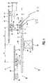
- FIG. 1is a schematic side view of an example of a device for directing radiation to a spot on a layer
- FIG. 2is a schematic, cross-sectional view of a distal end portion of a first example of an optical system for a device as shown in FIG. 1 , of a layer to which the radiation is directed and of a liquid flow maintained in operation;
- FIG. 3is a schematic, bottom view along the line III-III in FIG. 2
- FIG. 4is a schematic, cross-sectional view of a distal end portion of a third example of an optical system for a device as shown in FIG. 1 , of a layer to which the radiation is directed and of a liquid flow maintained in operation;
- FIG. 5is a schematic, bottom view along the line V-V in FIG. 4 ;
- FIG. 6is a schematic top plan view representation of a wafer stepper/scanner for optical lithography.
- a disc-shaped substrate 3 of glasscarrying a thin photosensitive layer 5 on one of its two sides is irradiated by means of a modulated radiation beam 7 , for instance a DUV laser beam with a wavelength of approximately 260 nm.
- a modulated radiation beam 7for instance a DUV laser beam with a wavelength of approximately 260 nm.
- an example 25 of a device in accordance with the inventionwhich device is described hereinafter with reference to FIGS. 1-3 .
- the radiation beam 7is focused to a scanning spot 11 on the photosensitive layer 5 by an optical system, according to the present example in the form of a lens system 9 , including a plurality of optical elements in the form of lenses.
- the lens system 9includes an objective lens 55 , which is secured in a lens holder 57 .
- the lens system 9further includes a most distal lens 59 , which is the one of the optical elements of the lens system 9 that is located nearest to the layer 5 when in operation.
- An interspace 53is maintained between the layer 5 that is irradiated and the one of the optical elements of the lens system 9 that is located nearest to the layer 5 .
- the optical elementsmay also include other items than lenses, such as filters, shields, diffraction gratings or mirrors.
- the layer 5 and the lens system 9are displaced with respect to each other, so that the modulated radiation beam 7 on the photosensitive layer 5 successively irradiates a series of spaced apart irradiated portions of the layer 5 and does not irradiate portions of the layer 5 in-between the irradiated portions.
- the irradiated photosensitive layer 5is subsequently developed by means of a developing liquid, which dissolves the irradiated elements 13 and leaves the non-irradiated elements 15 on the substrate 3 . It is also possible to provide that the irradiated portions are left while the non-irradiated portions are dissolved.
- a series of pits or bumpswhich corresponds to the desired series of pit-shaped information elements on the information carrier, are formed in the photosensitive layer 5 .
- the photosensitive layer 5is subsequently covered with a comparatively thin layer of for instance nickel by means of a sputtering process. Subsequently, this thin layer is covered with a comparatively thick nickel layer in an electro deposition process.
- the pattern of pits formed in the photosensitive layer 5leaves a corresponding pattern that is a negative of the pattern to be formed in the information carrier to be manufactured, i.e.
- the master moldcomprises a series of raised portions, which correspond to the series of pit-shaped elements formed in the photosensitive layer 5 and to the desired series of pit-shaped information elements on the information carrier.
- the master moldis thus rendered suitable for use as a mold in an injection-molding machine for injection molding the desired information carriers.
- a copy of the master moldis used as the mold for injection molding instead of the master mold, which copy of the master mold is commonly referred to as daughter mold, which is manufactured by means of the master mold using a customary replica process which is known per se.
- the substrate 3 with the photosensitive layer 5is placed on a table 27 that is rotatable about an axis of rotation 29 , which extends perpendicularly to the table 27 and the substrate 3 .
- the tablecan be driven by means of a first electromotor 31 .
- the device 25further comprises a radiation source 33 , which, in the example shown, is a laser source, which is secured in a fixed position to a frame 35 of the device 25 . It is observed that, as an alternative, the radiation may also be obtained from outside the device. Control over the radiation directed to the layer 5 can be achieved in many ways, for instance by controlling the radiation source 33 and/or by controlling a shutter or radiation diverter (not shown) between the radiation source 33 and the layer 5 .
- the optical lens system 9is secured onto a first traveller 37 , which can be displaced radially (parallel to the X-direction in the drawings) relative to the axis of rotation 29 , by means of a first displacement structure 39 .
- the first displacement structure 39includes a second electromotor 41 by means of which the first traveller 37 can be displaced over a straight guide 43 , which extends parallel to the X-direction and is fixed relative to the frame 35 .
- a mirror 45 in line with an optical axis 49 of the lens system 9is also secured to the first traveller 37 .
- the radiation beam 7 generated by the radiation source 33follows a radiation beam path 47 extending parallel to the X-direction, and the radiation beam 7 is deflected by the mirror 45 in a direction parallel to the optical axis 49 of the lens system 9 .
- the lens system 9can be displaced in the direction of its optical axis 49 by means of a focus actuator 51 , over comparatively small distances with respect to the first traveller 37 , so that the radiation beam 7 can be focused on the photosensitive layer 5 .
- the table 27 with the substrate 5is rotated about the axis of rotation 29 at a comparatively high speed by means of the first motor 31 , and the lens system 9 is displaced parallel to the X-direction by means of the second motor 41 at a comparatively low speed, so that the scanning spot 11 where the radiation beam 7 hits the layer follows a spiral-shaped track over the photosensitive layer 5 , leaving a trail of irradiated and non-irradiated elements extending in accordance with this spiral-shaped track.
- the device 25can suitably be used to manufacture master molds having a comparatively high information density, i.e. by means of the device 25 , a comparatively large number of irradiated elements can be provided per unit area of the photosensitive layer 5 .
- the attainable information densityincreases as the scanning spot 11 is smaller.
- the size of the scanning spot 11is determined by the wavelength of the radiation beam 7 and by the numerical aperture of the lens system 9 , the numerical aperture depending upon the optical refractive index of the medium present between the lens system 9 and the photosensitive layer 5 .
- the scanning spot 11is smaller as the refractive index of the medium present between the lens system 9 and the photosensitive layer 5 is larger.
- Liquidstypically have a much larger optical refractive index than air and therefore the portion of the interspace 53 between the lens system 9 and the photosensitive layer 5 through which the beam 7 extends is maintained filled with a liquid—according to this example water.
- wateris also particularly suitable because it is transparent to the DUV radiation beam 7 used and it does not attack the photosensitive layer 5 .
- the device 25further includes a liquid removal structure 77 , which is provided with a pick-up mouth 79 .
- the pick-up mouth 79is secured onto a second traveller 81 of the device 25 , which can be displaced by means of a second displacement structure 83 of the device 25 in a radial direction with respect to the axis of rotation 29 , according to the present example parallel to the X-direction, but another radial direction of displacement may be provided.
- the second displacement device 83For driving the displacement of the second traveller 81 , the second displacement device 83 comprises a third electromotor 85 connected to the second traveller 81 for displacing the second traveller over a straight guide 87 , which is attached to the frame 35 and extends in the directions of displacement of the second traveller 81 .
- the pick-up mouth 79is displaced by means of the third motor 85 .
- the third motor 85is controlled so that the lens system 9 and the pick-up mouth 79 are continuously situated at substantially equal distances R from the axis of rotation 29 of the substrate 3 .
- the pick-up mouth 79is maintained in a position downstream from the lens system 9 where irradiated portions of the layer 5 pass, so that the liquid supplied at the location of the lens system 9 is entrained by the rotating layer 5 to the pick-up mouth 79 where the liquid is subsequently picked-up from the photosensitive layer 5 by the pick-up mouth 79 .
- the pick-up mouth 79is always at a distance R from the axis of rotation 29 which corresponds to the distance R at which the lens system 9 is situated from the axis of rotation 29 , both the size and the capacity of the pick-up mouth 79 need only to be comparatively small to remove liquid that has already been used.
- FIGS. 2 and 3show, in more detail, the lens system 9 , the substrate 3 with the photosensitive layer 5 , and the interspace 53 between the photosensitive layer 5 and the lens system 9 .
- the lens 59 nearest to the layer 5has an optical surface 63 facing the substrate 3 and nearest to the substrate 3 .
- the lenses 55 , 59are suspended in a housing 61 , which includes a flat wall 65 , which faces the layer 5 and which substantially extends in an imaginary plane perpendicular to the optical axis of the lens 59 nearest to the layer 5 .
- a recess 92facing the spot 11 to which the radiation 7 is directed is provided in the surface of the lens system nearest to the layer 5 .
- the surface 63 of the lens 59 nearest to the layer 5forms an internal surface of the recess 92 .
- This surface 63also bounds the portion of the interspace 53 through which the radiation 7 irradiates the spot 11 .
- the surface 63 of the lens 59 nearest to the layer 5is concave so that the deepest point of the recess 92 is in the middle, however, this surface may also be flat or convex.
- the portion of the interspace 53 through which the radiation 7 irradiates the spot 11 on the layer 5is maintained filled with liquid 91 .
- the liquid 91is, at least to some extent, protected against being entrained from the interspace 53 . Since, the liquid 91 is less susceptible to being entrained away from the portion of the interspace 53 through which the radiation passes to the spot 11 , occurrence of the associated optical distortion caused by the portion of the interspace 53 through which the radiation passes not being completely filled with liquid is thus counteracted.
- thisallows the smallest size of the interspace 53 measured parallel to the optical axis of the lenses 55 , 59 to be relatively large. In turn, this reduces the risk of damage to the lens 59 nearest to the layer 5 and the allowable tolerances on the tilt of the lens can be larger without increasing the risk of the lens 59 touching the layer 5 .
- the recess 92may for instance be positioned and of such dimensions, so that only a portion of the radiation passes through the recess.
- the recess 92has a rim portion 94 closest to the layer 5 , which extends around the radiation 7 irradiating the spot 11 . Accordingly, the portion of the interspace 53 in the recess 92 in which liquid 91 is shielded from being entrained extends throughout the whole cross-section of the radiation beam.
- the optimum working distance between the layer 5 and the wall 65i.e. the portion of the lens assembly nearest to the layer 5 , is determined by two factors. On the one hand, the distance should be large enough to retain sufficient tolerance on the distance between the substrate 3 and arrangement of the lenses 55 , 59 and the housing 61 . On the other hand, this distance should not be too large because this would require a too large liquid flow to maintain the immersed condition of the portion of the interspace 53 through which the radiation passes to the spot 11 .
- a presently preferred range for the smallest thickness of the interspace 53is 3-1500 ⁇ m and more preferably 3-500 ⁇ m if the liquid is water larger values for the smallest thickness of the interspace can be particularly advantageous if the liquid has a larger viscosity than water.
- the overall width of the outflow openingaffects the upper end of the preferred range for the smallest thickness of the interspace, the smallest thickness of the interspace being preferably smaller than (100+ 1/20*W) ⁇ m in which W is the overall width of the outflow opening measured in a plane parallel to the layer 5 .
- the smallest thickness of the interspacemay be larger than approximately 10 ⁇ m, for instance larger than 15 ⁇ m, 30 ⁇ m or even 100 ⁇ m, to increase the insensitivity to tolerances.
- liquid outflowis preferably such that a liquid volume between the wall 65 and the layer 5 is maintained which includes a portion of the interspace 53 upstream (in a direction opposite to the direction of relative movement of the layer 5 in the area of the spot 11 ) of the portion of the interspace 53 through which the radiation irradiates the spot 11 .
- a safety margin of liquid upstreamis formed which ensures that variations in the distance over which liquid is urged in upstream direction do not cause a disruption of the filled condition of the portion of the interspace 53 through which the radiation 7 passes to the spot 11 .
- the most downstream outflow opening 90 in the lens system 9 through which the liquid 91 is passedhas a total projected cross-sectional passage area in a plane parallel to the layer 5 of which, seen in a direction parallel to the optical axis of the lens system 109 , the centre is located inside the portion of the interspace 53 through which the radiation 7 irradiates the spot 11 . Accordingly, the average path along which liquid flows out is at least to a large extent centred relative to the portion of the interspace 53 through which radiation passes to the spot 11 . Accordingly, the direction of movement of the layer 5 and the lens arrangement 9 relative to each other in the area of the spot 11 can be varied substantially without disrupting complete immersion of the portion of the interspace 53 through which the spot 11 is irradiated.
- the portion of the interspace 53 through which the radiation 7 irradiates the spot 11is also centrally located relative to the outflow opening 90 to such an extent that the trace 95 of liquid 91 fed from the outflow opening 90 into the interspace 53 completely immerses the portion of the interspace 53 through which the radiation 7 irradiates the spot 11 , not only while, in the position of the spot 11 , the layer 5 and the at least one lens system 9 move relative to each other in the direction indicated by the arrow 52 (which indicates the direction of movement of the layer 5 relative to the lens system 9 ), but also while, in the position of the spot 11 , the layer 5 and lens system 9 move relative to each other in opposite direction.
- the advantage of a comparatively large refractive index between the lens system and the medium between the lens system and the irradiated surfaceis that the image can be projected with a higher resolution, which in turn allows further miniaturization and/or an improved reliability.
- FIG. 6An example of such applications is optical projection lithography for the processing of wafers for the manufacture of semiconductor devices.
- An apparatus and a method for this purposeare schematically illustrated in FIG. 6 .
- Wafer steppers and wafer scannersare commercially available. Accordingly, such methods and apparatus are not described in great detail, but primarily to provide an understanding of liquid immersion as proposed in the present application in the context of such optical imaging applications.
- the projection lithography apparatusincludes a wafer support 12 and a projector 113 having a lens assembly 14 above the wafer support 12 .
- the wafer support 12carries a wafer 15 on which a plurality of areas 16 are intended to be irradiated by a beam projecting an image or partial image of a mask or reticle 17 in a scanner 18 operatively connected to the projector 113 .
- the support tableis moveable in X and Y direction along spindles 19 , 20 driven by spindle drives 21 , 22 .
- the spindle drives 21 , 22 and the scanner 18are connected to a control unit 23 .
- the projectorprojects a complete image of the reticle onto one of the areas 16 on the wafer 15 .
- the light beamis switched off or obscured and the wafer 15 is moved by the spindle drives 21 , 22 until a next area 16 of the wafer is in the required position in front of the lens assembly 14 .
- thismay involve relatively quick movement of the lens assembly 14 along the surface of the wafer in widely varying directions.
- the size of the irradiated spot on the surface of the wafer in which the image of the reticle is projectedis typically about 20 ⁇ 20 mm, but larger and smaller spots are conceivable.
- the wafer scanner modeIn particular when it is desired to manufacture larger semiconductor units, it is advantageous to project the image in the other mode, usually referred to as the wafer scanner mode. In that mode, only a slit-shaped portion of the reticle is projected as a slit shaped spot having a length that is several (for instance four or more times) times larger than its width in an area 16 on the surface of the wafer 15 .
- a typical size for the spotis for instance 30 ⁇ 5 mm).
- the reticle 17 to be scannedis moved along the scanning window while the wafer support 12 is synchronously moved relative to the lens assembly 14 under control of the control unit 23 with a velocity adapted so that only the projection spot, but not the scanned partial image portions of the reticle 17 that are projected on the wafer move relative to the wafer 15 .
- the image of the reticle 17is transferred to an area 16 of the wafer as successive portions “unroll” as the spot progresses over the wafer.
- the movement of the wafer 15 relative to the lens assembly 14 while a running window portion of the reticle is projected onto the wafer 15is usually carried out relatively slowly and usually each time in the same direction.
- the wafer 15is generally moved much more quickly relative to the lens assembly 14 to bring a next area of the wafer 15 where a next image of the or a reticle 17 is to be projected in front of the lens assembly 14 .
- This movementis carried out in widely varying directions dependent on the relative positions of the exposed area 16 of the wafer 15 and the next area 16 of the wafer 15 to be exposed.
- the lens or the lens and the wafermay be moved), it is advantageous if the liquid volume in the interspace between the lens 14 and the surface of the wafer 15 through which the radiation passes is immediately filled with liquid after completion of that movement, so that the space is reliably immersed before radiation is recommenced.
- watercan be used, for instance if the radiation is light of a wavelength of 193 nm. However in some circumstances other liquids may be more suitable.
- the recess 92is bound by a concave portion of the surface 63 of the lens 59 nearest to the spot 11 on the layer 5 to which the beam of radiation 7 is directed, the advantages of having a recess 92 are combined with a relatively uniform flow pattern throughout the portion 94 of the interspace 53 through which radiation 7 passes to the spot 11 .
- a uniform pattern of flow velocity gradients in the interspace 53is obtained.
- the relatively uniform flow patternis advantageous to avoid inducing vibrations and for obtaining a continuous uniform supply of fresh liquid and thereby a uniform, steady liquid temperature.
- the circle designated by reference numeral 94indicates the perimeter of the portion of the interspace 53 between the lens 59 and the layer 5 through which the radiation beam 7 passes.
- a liquid supply conduit 67extends through the housing 61 and leads to an outflow opening 90 .
- the outflow opening 90has the form of a canal structure in a surface 54 , which canal structure 67 is open towards the layer 5 , for distributing supplied liquid 91 longitudinally along the canal 67 and dispensing distributed liquid towards the layer 5 .
- the liquid 91is distributed by the canal structure 67 longitudinally along that canal structure and the liquid 91 is dispensed from the canal structure 67 towards the layer 5 .
- the canal 67can have various forms.
- the canalis formed such that the outflow opening 90 is located outside the radiation beam 7 and extends around the portion 94 of the interspace 53 through which the radiation 7 irradiates the spot 11 .
- the cross 96indicates the centre, seen in a direction parallel to the optical axis of the lens system 9 , of the total cross-sectional passage area of the outflow opening 90 .
- the liquid 91is preferably supplied at a pressure drop over the liquid between the canal structure 67 and the environment that is just sufficient to keep portion of the interspace 53 through which the radiation passes reliably immersed. Thus, the amount of water fed to the surface is kept to a minimum.
- the smallest thickness of the interspace 153(in this example the distance between the layer 5 and the surface 54 of the wall portion 65 ) may be larger, without causing an undue risk of disrupting the immersion of the portion 94 of the interspace through which the radiation passes. Therefore, when the liquid is dispensed from a canal-shaped outflow opening 90 , the displacement structure 39 , 83 and the lens system 9 are preferably positioned and dimensioned for maintaining the smallest thickness of the interspace 53 in a range between 3 and 500 ⁇ m.
- the flow rate with which the liquid 91 is suppliedis preferably such that it can be reliably ensured that a laminar flow with an essentially linear velocity profile and preferably a homogeneous Couette flow is present in the interspace 53 .
- a flowexerts a substantially constant force on the wall 65 in which the canal 67 is provided and on the side 63 of the lens 59 nearest to the layer 5 .
- the liquid present in the interspace 53exerts substantially no variable liquid forces on the lens system 9 .
- Such varying liquid forceswould lead to undesirable vibrations of the lens system 9 and hence to focusing errors and positioning errors of the radiation beam 7 on the photosensitive layer 5 .
- the flowis preferably free of air inclusions, so that the radiation beam 7 is not disturbed.
- FIGS. 4 and 5a second example of a lens system 109 for devices such as the devices shown in FIGS. 1 and 6 is shown.
- the outflow opening 190 downstream of the liquid supply canal 167is also provided with a canal structure open towards the layer 5 (i.e. in the direction in which the beam 107 is directed), but has a different, rectangular shape when seen in axial direction of the lens system 109 .
- An essentially rectangular shapeis particularly advantageous for reliably immersing a rectangular area 194 of the interspace intersected by the radiation beam while maintaining a uniform liquid flow patter throughout the intersected portion 194 of the interspace 153 , in particular if the movement of the lens system 109 and the layer 5 relative to each other is in a direction perpendicular to one of the sides of the rectangular canal structure 190 .
- Such circumstancestypically occur in optical projection lithography.
- the recess 192is bounded by a passage 195 in a wall 165 perpendicular to the axis of the lens system 9 and a surface of the lens 159 nearest to the spot 11 and the surface of the lens 159 nearest to the spot 11 also bounds the portion 194 of the interspace 153 through which the radiation 107 passes to the spot 11 . Accordingly, the lens 159 is effectively protected against damage due to inadvertent contact between the lens system 109 and the layer 5 on the substrate 3 .
Landscapes
- Physics & Mathematics (AREA)
- Optics & Photonics (AREA)
- Engineering & Computer Science (AREA)
- Manufacturing & Machinery (AREA)
- General Physics & Mathematics (AREA)
- Exposure And Positioning Against Photoresist Photosensitive Materials (AREA)
- Manufacturing Optical Record Carriers (AREA)
- Optical Head (AREA)
- Crystals, And After-Treatments Of Crystals (AREA)
- Heating, Cooling, Or Curing Plastics Or The Like In General (AREA)
- Physical Or Chemical Processes And Apparatus (AREA)
- Recrystallisation Techniques (AREA)
Abstract
Description
Claims (8)
Applications Claiming Priority (3)
| Application Number | Priority Date | Filing Date | Title |
|---|---|---|---|
| EP02080376 | 2002-12-19 | ||
| EP02080376.3 | 2002-12-19 | ||
| PCT/IB2003/005708WO2004057590A1 (en) | 2002-12-19 | 2003-11-20 | Method and device for irradiating spots on a layer |
Publications (2)
| Publication Number | Publication Date |
|---|---|
| US20060209414A1 US20060209414A1 (en) | 2006-09-21 |
| US7399978B2true US7399978B2 (en) | 2008-07-15 |
Family
ID=32668762
Family Applications (1)
| Application Number | Title | Priority Date | Filing Date |
|---|---|---|---|
| US10/539,351Expired - Fee RelatedUS7399978B2 (en) | 2002-12-19 | 2003-11-20 | Method and device for irradiating spots on a layer |
Country Status (11)
| Country | Link |
|---|---|
| US (1) | US7399978B2 (en) |
| EP (2) | EP1584089B1 (en) |
| JP (1) | JP4364806B2 (en) |
| KR (1) | KR100971441B1 (en) |
| CN (1) | CN100385535C (en) |
| AT (1) | ATE335272T1 (en) |
| AU (1) | AU2003283717A1 (en) |
| DE (1) | DE60307322T2 (en) |
| ES (1) | ES2268450T3 (en) |
| TW (1) | TWI288403B (en) |
| WO (1) | WO2004057590A1 (en) |
Cited By (5)
| Publication number | Priority date | Publication date | Assignee | Title |
|---|---|---|---|---|
| US20050259234A1 (en)* | 2002-12-10 | 2005-11-24 | Nikon Corporation | Exposure apparatus and device manufacturing method |
| US20100177292A1 (en)* | 2004-11-12 | 2010-07-15 | Asml Netherlands B.V. | Lithographic apparatus and device manufacturing method |
| US7812925B2 (en) | 2003-06-19 | 2010-10-12 | Nikon Corporation | Exposure apparatus, and device manufacturing method |
| US8035795B2 (en) | 2003-04-11 | 2011-10-11 | Nikon Corporation | Apparatus and method for maintaining immersion fluid in the gap under the protection lens during wafer exchange in an immersion lithography machine |
| US8045136B2 (en) | 2004-02-02 | 2011-10-25 | Nikon Corporation | Stage drive method and stage unit, exposure apparatus, and device manufacturing method |
Families Citing this family (250)
| Publication number | Priority date | Publication date | Assignee | Title |
|---|---|---|---|---|
| SG121822A1 (en) | 2002-11-12 | 2006-05-26 | Asml Netherlands Bv | Lithographic apparatus and device manufacturing method |
| US10503084B2 (en) | 2002-11-12 | 2019-12-10 | Asml Netherlands B.V. | Lithographic apparatus and device manufacturing method |
| US9482966B2 (en) | 2002-11-12 | 2016-11-01 | Asml Netherlands B.V. | Lithographic apparatus and device manufacturing method |
| KR100585476B1 (en) | 2002-11-12 | 2006-06-07 | 에이에스엠엘 네델란즈 비.브이. | Lithographic Apparatus and Device Manufacturing Method |
| DE60335595D1 (en) | 2002-11-12 | 2011-02-17 | Asml Netherlands Bv | Immersion lithographic apparatus and method of making a device |
| CN100568101C (en) | 2002-11-12 | 2009-12-09 | Asml荷兰有限公司 | Photolithography apparatus and device manufacturing method |
| US7110081B2 (en) | 2002-11-12 | 2006-09-19 | Asml Netherlands B.V. | Lithographic apparatus and device manufacturing method |
| US7372541B2 (en) | 2002-11-12 | 2008-05-13 | Asml Netherlands B.V. | Lithographic apparatus and device manufacturing method |
| CN101470360B (en) | 2002-11-12 | 2013-07-24 | Asml荷兰有限公司 | Immersion lithographic apparatus and device manufacturing method |
| SG131766A1 (en) | 2002-11-18 | 2007-05-28 | Asml Netherlands Bv | Lithographic apparatus and device manufacturing method |
| SG121829A1 (en) | 2002-11-29 | 2006-05-26 | Asml Netherlands Bv | Lithographic apparatus and device manufacturing method |
| JP4352874B2 (en) | 2002-12-10 | 2009-10-28 | 株式会社ニコン | Exposure apparatus and device manufacturing method |
| KR101101737B1 (en) | 2002-12-10 | 2012-01-05 | 가부시키가이샤 니콘 | Exposure apparatus, exposure method and method for manufacturing device |
| US7242455B2 (en) | 2002-12-10 | 2007-07-10 | Nikon Corporation | Exposure apparatus and method for producing device |
| US7948604B2 (en) | 2002-12-10 | 2011-05-24 | Nikon Corporation | Exposure apparatus and method for producing device |
| EP1571694A4 (en) | 2002-12-10 | 2008-10-15 | Nikon Corp | Exposure apparatus and method for manufacturing device |
| KR20120127755A (en) | 2002-12-10 | 2012-11-23 | 가부시키가이샤 니콘 | Exposure apparatus and method for manufacturing device |
| DE10261775A1 (en) | 2002-12-20 | 2004-07-01 | Carl Zeiss Smt Ag | Device for the optical measurement of an imaging system |
| EP2466623B1 (en) | 2003-02-26 | 2015-04-22 | Nikon Corporation | Exposure apparatus, exposure method, and method for producing device |
| KR20050110033A (en) | 2003-03-25 | 2005-11-22 | 가부시키가이샤 니콘 | Exposure system and device production method |
| EP1612850B1 (en) | 2003-04-07 | 2009-03-25 | Nikon Corporation | Exposure apparatus and method for manufacturing a device |
| WO2004093159A2 (en) | 2003-04-09 | 2004-10-28 | Nikon Corporation | Immersion lithography fluid control system |
| EP3352010A1 (en) | 2003-04-10 | 2018-07-25 | Nikon Corporation | Run-off path to collect liquid for an immersion lithography apparatus |
| EP3062152B1 (en) | 2003-04-10 | 2017-12-20 | Nikon Corporation | Environmental system including vaccum scavenge for an immersion lithography apparatus |
| EP2950147B1 (en) | 2003-04-10 | 2017-04-26 | Nikon Corporation | Environmental system including vaccum scavenge for an immersion lithography apparatus |
| CN101825847B (en) | 2003-04-11 | 2013-10-16 | 株式会社尼康 | Cleanup method for optics in immersion lithography |
| JP4582089B2 (en) | 2003-04-11 | 2010-11-17 | 株式会社ニコン | Liquid jet recovery system for immersion lithography |
| SG194246A1 (en) | 2003-04-17 | 2013-11-29 | Nikon Corp | Optical arrangement of autofocus elements for use with immersion lithography |
| TWI295414B (en) | 2003-05-13 | 2008-04-01 | Asml Netherlands Bv | Lithographic apparatus and device manufacturing method |
| KR20060009356A (en) | 2003-05-15 | 2006-01-31 | 가부시키가이샤 니콘 | Exposure apparatus and device manufacturing method |
| TWI421906B (en) | 2003-05-23 | 2014-01-01 | 尼康股份有限公司 | An exposure method, an exposure apparatus, and an element manufacturing method |
| TW201806001A (en) | 2003-05-23 | 2018-02-16 | 尼康股份有限公司 | Exposure device and device manufacturing method |
| KR101548832B1 (en) | 2003-05-28 | 2015-09-01 | 가부시키가이샤 니콘 | Exposure method, exposure device, and device manufacturing method |
| TWI442694B (en) | 2003-05-30 | 2014-06-21 | Asml Netherlands Bv | Lithographic apparatus and device manufacturing method |
| US7213963B2 (en) | 2003-06-09 | 2007-05-08 | Asml Netherlands B.V. | Lithographic apparatus and device manufacturing method |
| US7317504B2 (en) | 2004-04-08 | 2008-01-08 | Asml Netherlands B.V. | Lithographic apparatus and device manufacturing method |
| EP2261741A3 (en) | 2003-06-11 | 2011-05-25 | ASML Netherlands B.V. | Lithographic apparatus and device manufacturing method |
| KR101242815B1 (en) | 2003-06-13 | 2013-03-12 | 가부시키가이샤 니콘 | Exposure method, substrate stage, exposure apparatus and method for manufacturing device |
| US6867844B2 (en) | 2003-06-19 | 2005-03-15 | Asml Holding N.V. | Immersion photolithography system and method using microchannel nozzles |
| EP1491956B1 (en) | 2003-06-27 | 2006-09-06 | ASML Netherlands B.V. | Lithographic apparatus and device manufacturing method |
| EP1498778A1 (en) | 2003-06-27 | 2005-01-19 | ASML Netherlands B.V. | Lithographic apparatus and device manufacturing method |
| EP1494075B1 (en) | 2003-06-30 | 2008-06-25 | ASML Netherlands B.V. | Lithographic projection apparatus and device manufacturing method |
| EP1494074A1 (en) | 2003-06-30 | 2005-01-05 | ASML Netherlands B.V. | Lithographic apparatus and device manufacturing method |
| KR20060027832A (en) | 2003-07-01 | 2006-03-28 | 가부시키가이샤 니콘 | Method of Using Isotopically Specified Fluids as Optical Elements |
| EP3179309A1 (en) | 2003-07-08 | 2017-06-14 | Nikon Corporation | Wafer table for immersion lithography |
| EP1643543B1 (en) | 2003-07-09 | 2010-11-24 | Nikon Corporation | Exposure apparatus and method for manufacturing device |
| WO2005006418A1 (en) | 2003-07-09 | 2005-01-20 | Nikon Corporation | Exposure apparatus and method for manufacturing device |
| WO2005006415A1 (en) | 2003-07-09 | 2005-01-20 | Nikon Corporation | Exposure apparatus and method for manufacturing device |
| SG109000A1 (en) | 2003-07-16 | 2005-02-28 | Asml Netherlands Bv | Lithographic apparatus and device manufacturing method |
| EP1500982A1 (en) | 2003-07-24 | 2005-01-26 | ASML Netherlands B.V. | Lithographic apparatus and device manufacturing method |
| WO2005010960A1 (en) | 2003-07-25 | 2005-02-03 | Nikon Corporation | Inspection method and inspection device for projection optical system, and production method for projection optical system |
| EP1503244A1 (en) | 2003-07-28 | 2005-02-02 | ASML Netherlands B.V. | Lithographic projection apparatus and device manufacturing method |
| US7326522B2 (en) | 2004-02-11 | 2008-02-05 | Asml Netherlands B.V. | Device manufacturing method and a substrate |
| US7175968B2 (en) | 2003-07-28 | 2007-02-13 | Asml Netherlands B.V. | Lithographic apparatus, device manufacturing method and a substrate |
| KR101641011B1 (en) | 2003-07-28 | 2016-07-19 | 가부시키가이샤 니콘 | Exposure apparatus, device producing method, and exposure apparatus controlling method |
| US7779781B2 (en) | 2003-07-31 | 2010-08-24 | Asml Netherlands B.V. | Lithographic apparatus and device manufacturing method |
| US8149381B2 (en) | 2003-08-26 | 2012-04-03 | Nikon Corporation | Optical element and exposure apparatus |
| JP4474652B2 (en) | 2003-08-26 | 2010-06-09 | 株式会社ニコン | Optical element and exposure apparatus |
| US6954256B2 (en) | 2003-08-29 | 2005-10-11 | Asml Netherlands B.V. | Gradient immersion lithography |
| EP2261740B1 (en) | 2003-08-29 | 2014-07-09 | ASML Netherlands BV | Lithographic apparatus |
| KR101380989B1 (en) | 2003-08-29 | 2014-04-04 | 가부시키가이샤 니콘 | Exposure apparatus and device producing method |
| TWI263859B (en) | 2003-08-29 | 2006-10-11 | Asml Netherlands Bv | Lithographic apparatus and device manufacturing method |
| TWI245163B (en) | 2003-08-29 | 2005-12-11 | Asml Netherlands Bv | Lithographic apparatus and device manufacturing method |
| EP3223053A1 (en) | 2003-09-03 | 2017-09-27 | Nikon Corporation | Apparatus and method for providing fluid for immersion lithography |
| JP4444920B2 (en) | 2003-09-19 | 2010-03-31 | 株式会社ニコン | Exposure apparatus and device manufacturing method |
| EP2837969B1 (en) | 2003-09-29 | 2016-04-20 | Nikon Corporation | Exposure apparatus, exposure method, and method for producing device |
| EP1519230A1 (en) | 2003-09-29 | 2005-03-30 | ASML Netherlands B.V. | Lithographic apparatus and device manufacturing method |
| EP1519231B1 (en) | 2003-09-29 | 2005-12-21 | ASML Netherlands B.V. | Lithographic apparatus and device manufacturing method |
| US7158211B2 (en) | 2003-09-29 | 2007-01-02 | Asml Netherlands B.V. | Lithographic apparatus and device manufacturing method |
| KR101203028B1 (en) | 2003-10-08 | 2012-11-21 | 가부시키가이샤 자오 니콘 | Substrate carrying apparatus, substrate carrying method, exposure apparatus, exposure method, and method for producing device |
| KR20060126949A (en) | 2003-10-08 | 2006-12-11 | 가부시키가이샤 니콘 | Substrate conveyance apparatus and substrate conveyance method, exposure apparatus, exposure method, and device manufacturing method |
| JP2005136364A (en) | 2003-10-08 | 2005-05-26 | Zao Nikon Co Ltd | Substrate transport apparatus, exposure apparatus, and device manufacturing method |
| TWI553701B (en) | 2003-10-09 | 2016-10-11 | 尼康股份有限公司 | Exposure apparatus and exposure method, component manufacturing method |
| EP1524558A1 (en) | 2003-10-15 | 2005-04-20 | ASML Netherlands B.V. | Lithographic apparatus and device manufacturing method |
| EP1524557A1 (en) | 2003-10-15 | 2005-04-20 | ASML Netherlands B.V. | Lithographic apparatus and device manufacturing method |
| US7411653B2 (en) | 2003-10-28 | 2008-08-12 | Asml Netherlands B.V. | Lithographic apparatus |
| WO2005041276A1 (en) | 2003-10-28 | 2005-05-06 | Nikon Corporation | Exposure apparatus, exposure method, and device producing method |
| US7352433B2 (en) | 2003-10-28 | 2008-04-01 | Asml Netherlands B.V. | Lithographic apparatus and device manufacturing method |
| US7528929B2 (en) | 2003-11-14 | 2009-05-05 | Asml Netherlands B.V. | Lithographic apparatus and device manufacturing method |
| US7545481B2 (en) | 2003-11-24 | 2009-06-09 | Asml Netherlands B.V. | Lithographic apparatus and device manufacturing method |
| KR101394764B1 (en) | 2003-12-03 | 2014-05-27 | 가부시키가이샤 니콘 | Exposure apparatus, exposure method, device producing method, and optical component |
| JP4720506B2 (en) | 2003-12-15 | 2011-07-13 | 株式会社ニコン | Stage apparatus, exposure apparatus, and exposure method |
| US7460206B2 (en) | 2003-12-19 | 2008-12-02 | Carl Zeiss Smt Ag | Projection objective for immersion lithography |
| US7394521B2 (en) | 2003-12-23 | 2008-07-01 | Asml Netherlands B.V. | Lithographic apparatus and device manufacturing method |
| US7589818B2 (en) | 2003-12-23 | 2009-09-15 | Asml Netherlands B.V. | Lithographic apparatus, alignment apparatus, device manufacturing method, and a method of converting an apparatus |
| DE602005019689D1 (en) | 2004-01-20 | 2010-04-15 | Zeiss Carl Smt Ag | EXPOSURE DEVICE AND MEASURING DEVICE FOR A PROJECTION SECTOR |
| WO2005076321A1 (en) | 2004-02-03 | 2005-08-18 | Nikon Corporation | Exposure apparatus and method of producing device |
| KR101309428B1 (en) | 2004-02-04 | 2013-09-23 | 가부시키가이샤 니콘 | Exposure apparatus, exposure method, and device producing method |
| US7050146B2 (en) | 2004-02-09 | 2006-05-23 | Asml Netherlands B.V. | Lithographic apparatus and device manufacturing method |
| CN101727021A (en)* | 2004-02-13 | 2010-06-09 | 卡尔蔡司Smt股份公司 | Projection objective for a microlithographic projection exposure apparatus |
| DE102004013886A1 (en) | 2004-03-16 | 2005-10-06 | Carl Zeiss Smt Ag | Multiple Exposure Method, Microlithography Projection Exposure System and Projection System |
| KR101851511B1 (en) | 2004-03-25 | 2018-04-23 | 가부시키가이샤 니콘 | Exposure apparatus and method for manufacturing device |
| US7227619B2 (en) | 2004-04-01 | 2007-06-05 | Asml Netherlands B.V. | Lithographic apparatus and device manufacturing method |
| US7034917B2 (en) | 2004-04-01 | 2006-04-25 | Asml Netherlands B.V. | Lithographic apparatus, device manufacturing method and device manufactured thereby |
| US7295283B2 (en) | 2004-04-02 | 2007-11-13 | Asml Netherlands B.V. | Lithographic apparatus and device manufacturing method |
| US7898642B2 (en) | 2004-04-14 | 2011-03-01 | Asml Netherlands B.V. | Lithographic apparatus and device manufacturing method |
| WO2005104195A1 (en) | 2004-04-19 | 2005-11-03 | Nikon Corporation | Exposure apparatus and device producing method |
| US7379159B2 (en) | 2004-05-03 | 2008-05-27 | Asml Netherlands B.V. | Lithographic apparatus and device manufacturing method |
| US8054448B2 (en)* | 2004-05-04 | 2011-11-08 | Nikon Corporation | Apparatus and method for providing fluid for immersion lithography |
| US7616383B2 (en) | 2004-05-18 | 2009-11-10 | Asml Netherlands B.V. | Lithographic apparatus and device manufacturing method |
| US7486381B2 (en) | 2004-05-21 | 2009-02-03 | Asml Netherlands B.V. | Lithographic apparatus and device manufacturing method |
| CN100594430C (en) | 2004-06-04 | 2010-03-17 | 卡尔蔡司Smt股份公司 | System for measuring image quality of optical imaging system |
| EP3203498A1 (en) | 2004-06-09 | 2017-08-09 | Nikon Corporation | Exposure apparatus and device manufacturing method |
| US8717533B2 (en) | 2004-06-10 | 2014-05-06 | Nikon Corporation | Exposure apparatus, exposure method, and method for producing device |
| KR101178755B1 (en) | 2004-06-10 | 2012-08-31 | 가부시키가이샤 니콘 엔지니어링 | Exposure equipment, exposure method and device manufacturing method |
| US8508713B2 (en) | 2004-06-10 | 2013-08-13 | Nikon Corporation | Exposure apparatus, exposure method, and method for producing device |
| US8373843B2 (en) | 2004-06-10 | 2013-02-12 | Nikon Corporation | Exposure apparatus, exposure method, and method for producing device |
| EP3067749B1 (en) | 2004-06-10 | 2017-10-18 | Nikon Corporation | Exposure apparatus, exposure method, and method for producing device |
| US7481867B2 (en) | 2004-06-16 | 2009-01-27 | Edwards Limited | Vacuum system for immersion photolithography |
| US7463330B2 (en) | 2004-07-07 | 2008-12-09 | Asml Netherlands B.V. | Lithographic apparatus and device manufacturing method |
| JP4894515B2 (en) | 2004-07-12 | 2012-03-14 | 株式会社ニコン | Exposure apparatus, device manufacturing method, and liquid detection method |
| US7161663B2 (en) | 2004-07-22 | 2007-01-09 | Asml Netherlands B.V. | Lithographic apparatus |
| US7304715B2 (en) | 2004-08-13 | 2007-12-04 | Asml Netherlands B.V. | Lithographic apparatus and device manufacturing method |
| KR20070048164A (en) | 2004-08-18 | 2007-05-08 | 가부시키가이샤 니콘 | Exposure apparatus and device manufacturing method |
| US7701550B2 (en) | 2004-08-19 | 2010-04-20 | Asml Netherlands B.V. | Lithographic apparatus and device manufacturing method |
| KR101506100B1 (en) | 2004-09-17 | 2015-03-26 | 가부시키가이샤 니콘 | Exposure apparatus, exposure method, and method for manufacturing device |
| US7133114B2 (en) | 2004-09-20 | 2006-11-07 | Asml Netherlands B.V. | Lithographic apparatus and device manufacturing method |
| US7522261B2 (en) | 2004-09-24 | 2009-04-21 | Asml Netherlands B.V. | Lithographic apparatus and device manufacturing method |
| US7355674B2 (en) | 2004-09-28 | 2008-04-08 | Asml Netherlands B.V. | Lithographic apparatus, device manufacturing method and computer program product |
| US7894040B2 (en) | 2004-10-05 | 2011-02-22 | Asml Netherlands B.V. | Lithographic apparatus and device manufacturing method |
| US7209213B2 (en) | 2004-10-07 | 2007-04-24 | Asml Netherlands B.V. | Lithographic apparatus and device manufacturing method |
| WO2006041083A1 (en) | 2004-10-13 | 2006-04-20 | Nikon Corporation | Exposure apparatus, exposure method and device manufacturing method |
| US7119876B2 (en) | 2004-10-18 | 2006-10-10 | Asml Netherlands B.V. | Lithographic apparatus and device manufacturing method |
| US7379155B2 (en) | 2004-10-18 | 2008-05-27 | Asml Netherlands B.V. | Lithographic apparatus and device manufacturing method |
| CN101044594B (en) | 2004-10-26 | 2010-05-12 | 株式会社尼康 | Substrate processing method, exposure apparatus, and device manufacturing method |
| US7414699B2 (en) | 2004-11-12 | 2008-08-19 | Asml Netherlands B.V. | Lithographic apparatus and device manufacturing method |
| US7251013B2 (en) | 2004-11-12 | 2007-07-31 | Asml Netherlands B.V. | Lithographic apparatus and device manufacturing method |
| US7583357B2 (en) | 2004-11-12 | 2009-09-01 | Asml Netherlands B.V. | Lithographic apparatus and device manufacturing method |
| US7411657B2 (en) | 2004-11-17 | 2008-08-12 | Asml Netherlands B.V. | Lithographic apparatus and device manufacturing method |
| US7145630B2 (en) | 2004-11-23 | 2006-12-05 | Asml Netherlands B.V. | Lithographic apparatus and device manufacturing method |
| US7161654B2 (en) | 2004-12-02 | 2007-01-09 | Asml Netherlands B.V. | Lithographic apparatus and device manufacturing method |
| US7446850B2 (en) | 2004-12-03 | 2008-11-04 | Asml Netherlands B.V. | Lithographic apparatus and device manufacturing method |
| US7196770B2 (en) | 2004-12-07 | 2007-03-27 | Asml Netherlands B.V. | Prewetting of substrate before immersion exposure |
| US7248334B2 (en) | 2004-12-07 | 2007-07-24 | Asml Netherlands B.V. | Sensor shield |
| US7397533B2 (en) | 2004-12-07 | 2008-07-08 | Asml Netherlands B.V. | Lithographic apparatus and device manufacturing method |
| US7365827B2 (en) | 2004-12-08 | 2008-04-29 | Asml Netherlands B.V. | Lithographic apparatus and device manufacturing method |
| JP4752473B2 (en) | 2004-12-09 | 2011-08-17 | 株式会社ニコン | Exposure apparatus, exposure method, and device manufacturing method |
| US7352440B2 (en) | 2004-12-10 | 2008-04-01 | Asml Netherlands B.V. | Substrate placement in immersion lithography |
| US7403261B2 (en) | 2004-12-15 | 2008-07-22 | Asml Netherlands B.V. | Lithographic apparatus and device manufacturing method |
| US7528931B2 (en) | 2004-12-20 | 2009-05-05 | Asml Netherlands B.V. | Lithographic apparatus and device manufacturing method |
| US7880860B2 (en) | 2004-12-20 | 2011-02-01 | Asml Netherlands B.V. | Lithographic apparatus and device manufacturing method |
| US7405805B2 (en) | 2004-12-28 | 2008-07-29 | Asml Netherlands B.V. | Lithographic apparatus and device manufacturing method |
| US7491661B2 (en) | 2004-12-28 | 2009-02-17 | Asml Netherlands B.V. | Device manufacturing method, top coat material and substrate |
| US20060147821A1 (en) | 2004-12-30 | 2006-07-06 | Asml Netherlands B.V. | Lithographic apparatus and device manufacturing method |
| SG124351A1 (en)* | 2005-01-14 | 2006-08-30 | Asml Netherlands Bv | Lithographic apparatus and device manufacturing method |
| DE602006012746D1 (en) | 2005-01-14 | 2010-04-22 | Asml Netherlands Bv | Lithographic apparatus and manufacturing method |
| KR101513840B1 (en) | 2005-01-31 | 2015-04-20 | 가부시키가이샤 니콘 | Exposure apparatus and method for manufacturing device |
| US8692973B2 (en) | 2005-01-31 | 2014-04-08 | Nikon Corporation | Exposure apparatus and method for producing device |
| CN102360170B (en) | 2005-02-10 | 2014-03-12 | Asml荷兰有限公司 | Immersion liquid, exposure apparatus, and exposure process |
| US8018573B2 (en) | 2005-02-22 | 2011-09-13 | Asml Netherlands B.V. | Lithographic apparatus and device manufacturing method |
| US7224431B2 (en) | 2005-02-22 | 2007-05-29 | Asml Netherlands B.V. | Lithographic apparatus and device manufacturing method |
| US7378025B2 (en) | 2005-02-22 | 2008-05-27 | Asml Netherlands B.V. | Fluid filtration method, fluid filtered thereby, lithographic apparatus and device manufacturing method |
| US7282701B2 (en) | 2005-02-28 | 2007-10-16 | Asml Netherlands B.V. | Sensor for use in a lithographic apparatus |
| US7428038B2 (en) | 2005-02-28 | 2008-09-23 | Asml Netherlands B.V. | Lithographic apparatus, device manufacturing method and apparatus for de-gassing a liquid |
| US7324185B2 (en) | 2005-03-04 | 2008-01-29 | Asml Netherlands B.V. | Lithographic apparatus and device manufacturing method |
| US7684010B2 (en) | 2005-03-09 | 2010-03-23 | Asml Netherlands B.V. | Lithographic apparatus, device manufacturing method, seal structure, method of removing an object and a method of sealing |
| TWI424260B (en) | 2005-03-18 | 2014-01-21 | 尼康股份有限公司 | A board member, a substrate holding device, an exposure apparatus and an exposure method, and a device manufacturing method |
| US8638422B2 (en) | 2005-03-18 | 2014-01-28 | Nikon Corporation | Exposure method, exposure apparatus, method for producing device, and method for evaluating exposure apparatus |
| US7330238B2 (en) | 2005-03-28 | 2008-02-12 | Asml Netherlands, B.V. | Lithographic apparatus, immersion projection apparatus and device manufacturing method |
| JP4605219B2 (en) | 2005-03-30 | 2011-01-05 | 株式会社ニコン | Exposure condition determination method, exposure method and exposure apparatus, and device manufacturing method |
| US7411654B2 (en) | 2005-04-05 | 2008-08-12 | Asml Netherlands B.V. | Lithographic apparatus and device manufacturing method |
| USRE43576E1 (en) | 2005-04-08 | 2012-08-14 | Asml Netherlands B.V. | Dual stage lithographic apparatus and device manufacturing method |
| US7291850B2 (en) | 2005-04-08 | 2007-11-06 | Asml Netherlands B.V. | Lithographic apparatus and device manufacturing method |
| KR101555707B1 (en) | 2005-04-18 | 2015-09-25 | 가부시키가이샤 니콘 | Exposure apparatus, exposure method, and device manufacturing method |
| EP2527921A3 (en) | 2005-04-28 | 2017-10-18 | Nikon Corporation | Exposure method and exposure apparatus |
| US8248577B2 (en) | 2005-05-03 | 2012-08-21 | Asml Netherlands B.V. | Lithographic apparatus and device manufacturing method |
| US7317507B2 (en) | 2005-05-03 | 2008-01-08 | Asml Netherlands B.V. | Lithographic apparatus and device manufacturing method |
| US7433016B2 (en) | 2005-05-03 | 2008-10-07 | Asml Netherlands B.V. | Lithographic apparatus and device manufacturing method |
| US7751027B2 (en) | 2005-06-21 | 2010-07-06 | Asml Netherlands B.V. | Lithographic apparatus and device manufacturing method |
| US7652746B2 (en) | 2005-06-21 | 2010-01-26 | Asml Netherlands B.V. | Lithographic apparatus and device manufacturing method |
| US7834974B2 (en) | 2005-06-28 | 2010-11-16 | Asml Netherlands B.V. | Lithographic apparatus and device manufacturing method |
| US7468779B2 (en) | 2005-06-28 | 2008-12-23 | Asml Netherlands B.V. | Lithographic apparatus and device manufacturing method |
| US7474379B2 (en) | 2005-06-28 | 2009-01-06 | Asml Netherlands B.V. | Lithographic apparatus and device manufacturing method |
| KR20080026082A (en) | 2005-06-30 | 2008-03-24 | 가부시키가이샤 니콘 | Exposure apparatus and method, maintenance method of exposure apparatus, and device manufacturing method |
| US7535644B2 (en) | 2005-08-12 | 2009-05-19 | Asml Netherlands B.V. | Lens element, lithographic apparatus, device manufacturing method, and device manufactured thereby |
| US8054445B2 (en) | 2005-08-16 | 2011-11-08 | Asml Netherlands B.V. | Lithographic apparatus and device manufacturing method |
| TWI430039B (en) | 2005-08-23 | 2014-03-11 | 尼康股份有限公司 | An exposure apparatus and an exposure method, and an element manufacturing method |
| KR20080053497A (en)* | 2005-09-21 | 2008-06-13 | 가부시키가이샤 니콘 | Exposure apparatus and exposure method, and device manufacturing method |
| US7411658B2 (en) | 2005-10-06 | 2008-08-12 | Asml Netherlands B.V. | Lithographic apparatus and device manufacturing method |
| WO2007055199A1 (en) | 2005-11-09 | 2007-05-18 | Nikon Corporation | Exposure apparatus and method, and method for manufacturing device |
| US7804577B2 (en) | 2005-11-16 | 2010-09-28 | Asml Netherlands B.V. | Lithographic apparatus |
| US7656501B2 (en) | 2005-11-16 | 2010-02-02 | Asml Netherlands B.V. | Lithographic apparatus |
| US7864292B2 (en) | 2005-11-16 | 2011-01-04 | Asml Netherlands B.V. | Lithographic apparatus and device manufacturing method |
| JP2007165869A (en) | 2005-11-21 | 2007-06-28 | Nikon Corp | Exposure method, device manufacturing method using the same, exposure apparatus, and substrate processing method and apparatus |
| US7803516B2 (en) | 2005-11-21 | 2010-09-28 | Nikon Corporation | Exposure method, device manufacturing method using the same, exposure apparatus, and substrate processing method and apparatus |
| US7633073B2 (en) | 2005-11-23 | 2009-12-15 | Asml Netherlands B.V. | Lithographic apparatus and device manufacturing method |
| EP1970944A4 (en) | 2005-12-06 | 2010-04-28 | Nikon Corp | Exposure apparatus, exposure method, projection optical system and device manufacturing method |
| JP5194799B2 (en) | 2005-12-06 | 2013-05-08 | 株式会社ニコン | Exposure method, exposure apparatus, and device manufacturing method |
| US7782442B2 (en) | 2005-12-06 | 2010-08-24 | Nikon Corporation | Exposure apparatus, exposure method, projection optical system and device producing method |
| US7420194B2 (en) | 2005-12-27 | 2008-09-02 | Asml Netherlands B.V. | Lithographic apparatus and substrate edge seal |
| CN101326617B (en) | 2005-12-28 | 2012-06-20 | 株式会社尼康 | Pattern forming method, pattern forming device, and device manufacturing method |
| US7932994B2 (en) | 2005-12-28 | 2011-04-26 | Nikon Corporation | Exposure apparatus, exposure method, and method for producing device |
| US8953148B2 (en) | 2005-12-28 | 2015-02-10 | Nikon Corporation | Exposure apparatus and making method thereof |
| US7839483B2 (en) | 2005-12-28 | 2010-11-23 | Asml Netherlands B.V. | Lithographic apparatus, device manufacturing method and a control system |
| WO2007077925A1 (en) | 2005-12-28 | 2007-07-12 | Nikon Corporation | Pattern formation method, pattern formation device, and device fabrication method |
| US8411271B2 (en) | 2005-12-28 | 2013-04-02 | Nikon Corporation | Pattern forming method, pattern forming apparatus, and device manufacturing method |
| US7649611B2 (en) | 2005-12-30 | 2010-01-19 | Asml Netherlands B.V. | Lithographic apparatus and device manufacturing method |
| EP3147710B1 (en) | 2006-01-19 | 2019-04-10 | Nikon Corporation | Exposure apparatus, exposure method, and device manufacturing method |
| TW200801833A (en) | 2006-02-16 | 2008-01-01 | Nikon Corp | Exposure apparatus, exposure method and device manufacturing method |
| KR20080101865A (en) | 2006-02-16 | 2008-11-21 | 가부시키가이샤 니콘 | Exposure apparatus, exposure method, and device manufacturing method |
| EP1986223A4 (en) | 2006-02-16 | 2010-08-25 | Nikon Corp | Exposure apparatus, exposing method, and device manufacturing method |
| EP1986224A4 (en) | 2006-02-16 | 2012-01-25 | Nikon Corp | Exposure apparatus, exposing method, and device manufacturing method |
| CN101385120B (en) | 2006-02-21 | 2012-09-05 | 株式会社尼康 | Measuring apparatus and method, processing apparatus and method, pattern forming apparatus and method, exposure apparatus and method, and device manufacturing method |
| WO2007097380A1 (en) | 2006-02-21 | 2007-08-30 | Nikon Corporation | Pattern forming apparatus, pattern forming method, mobile object driving system, mobile body driving method, exposure apparatus, exposure method and device manufacturing method |
| CN101980084B (en) | 2006-02-21 | 2013-01-23 | 株式会社尼康 | Exposure apparatus, exposure method, and device manufacturing method |
| JP5077770B2 (en) | 2006-03-07 | 2012-11-21 | 株式会社ニコン | Device manufacturing method, device manufacturing system, and measurement / inspection apparatus |
| US8045134B2 (en) | 2006-03-13 | 2011-10-25 | Asml Netherlands B.V. | Lithographic apparatus, control system and device manufacturing method |
| WO2007105645A1 (en) | 2006-03-13 | 2007-09-20 | Nikon Corporation | Exposure apparatus, maintenance method, exposure method and device manufacturing method |
| US9477158B2 (en) | 2006-04-14 | 2016-10-25 | Asml Netherlands B.V. | Lithographic apparatus and device manufacturing method |
| DE102006021797A1 (en) | 2006-05-09 | 2007-11-15 | Carl Zeiss Smt Ag | Optical imaging device with thermal damping |
| TW200805000A (en) | 2006-05-18 | 2008-01-16 | Nikon Corp | Exposure method and apparatus, maintenance method and device manufacturing method |
| CN102109773A (en) | 2006-05-22 | 2011-06-29 | 株式会社尼康 | Exposure method, exposure apparatus, and maintenance method |
| US7969548B2 (en) | 2006-05-22 | 2011-06-28 | Asml Netherlands B.V. | Lithographic apparatus and lithographic apparatus cleaning method |
| EP2034515A4 (en) | 2006-05-23 | 2012-01-18 | Nikon Corp | Maintenance method, exposure method and apparatus, and device manufacturing method |
| JP5218049B2 (en) | 2006-05-31 | 2013-06-26 | 株式会社ニコン | Exposure apparatus and exposure method |
| EP2043134A4 (en) | 2006-06-30 | 2012-01-25 | Nikon Corp | Maintenance method, exposure method and apparatus and device manufacturing method |
| US8045135B2 (en) | 2006-11-22 | 2011-10-25 | Asml Netherlands B.V. | Lithographic apparatus with a fluid combining unit and related device manufacturing method |
| US8634053B2 (en) | 2006-12-07 | 2014-01-21 | Asml Netherlands B.V. | Lithographic apparatus and device manufacturing method |
| US9632425B2 (en) | 2006-12-07 | 2017-04-25 | Asml Holding N.V. | Lithographic apparatus, a dryer and a method of removing liquid from a surface |
| US7791709B2 (en) | 2006-12-08 | 2010-09-07 | Asml Netherlands B.V. | Substrate support and lithographic process |
| US8237911B2 (en) | 2007-03-15 | 2012-08-07 | Nikon Corporation | Apparatus and methods for keeping immersion fluid adjacent to an optical assembly during wafer exchange in an immersion lithography machine |
| JPWO2008132799A1 (en) | 2007-04-12 | 2010-07-22 | 株式会社ニコン | Measuring method, exposure method, and device manufacturing method |
| US7841352B2 (en) | 2007-05-04 | 2010-11-30 | Asml Netherlands B.V. | Cleaning device, a lithographic apparatus and a lithographic apparatus cleaning method |
| US7866330B2 (en) | 2007-05-04 | 2011-01-11 | Asml Netherlands B.V. | Cleaning device, a lithographic apparatus and a lithographic apparatus cleaning method |
| US8947629B2 (en) | 2007-05-04 | 2015-02-03 | Asml Netherlands B.V. | Cleaning device, a lithographic apparatus and a lithographic apparatus cleaning method |
| JP2009033111A (en) | 2007-05-28 | 2009-02-12 | Nikon Corp | Exposure apparatus, device manufacturing method, cleaning apparatus, cleaning method, and exposure method |
| US8164736B2 (en) | 2007-05-29 | 2012-04-24 | Nikon Corporation | Exposure method, exposure apparatus, and method for producing device |
| US8098362B2 (en) | 2007-05-30 | 2012-01-17 | Nikon Corporation | Detection device, movable body apparatus, pattern formation apparatus and pattern formation method, exposure apparatus and exposure method, and device manufacturing method |
| EP2017833A1 (en) | 2007-07-16 | 2009-01-21 | Nederlandse Organisatie voor toegepast- natuurwetenschappelijk onderzoek TNO | Scanned writing of an exposure pattern on a substrate |
| US8194232B2 (en) | 2007-07-24 | 2012-06-05 | Nikon Corporation | Movable body drive method and movable body drive system, pattern formation method and apparatus, exposure method and apparatus, position control method and position control system, and device manufacturing method |
| US8547527B2 (en) | 2007-07-24 | 2013-10-01 | Nikon Corporation | Movable body drive method and movable body drive system, pattern formation method and pattern formation apparatus, and device manufacturing method |
| JP5177449B2 (en) | 2007-07-24 | 2013-04-03 | 株式会社ニコン | Moving body driving method and moving body driving system, pattern forming method and apparatus, exposure method and apparatus, and device manufacturing method |
| US8023106B2 (en) | 2007-08-24 | 2011-09-20 | Nikon Corporation | Movable body drive method and movable body drive system, pattern formation method and apparatus, exposure method and apparatus, and device manufacturing method |
| US8218129B2 (en) | 2007-08-24 | 2012-07-10 | Nikon Corporation | Movable body drive method and movable body drive system, pattern formation method and apparatus, exposure method and apparatus, device manufacturing method, measuring method, and position measurement system |
| US8867022B2 (en) | 2007-08-24 | 2014-10-21 | Nikon Corporation | Movable body drive method and movable body drive system, pattern formation method and apparatus, and device manufacturing method |
| US8237919B2 (en) | 2007-08-24 | 2012-08-07 | Nikon Corporation | Movable body drive method and movable body drive system, pattern formation method and apparatus, exposure method and apparatus, and device manufacturing method for continuous position measurement of movable body before and after switching between sensor heads |
| US9304412B2 (en) | 2007-08-24 | 2016-04-05 | Nikon Corporation | Movable body drive method and movable body drive system, pattern formation method and apparatus, exposure method and apparatus, device manufacturing method, and measuring method |
| NL1036186A1 (en)* | 2007-12-03 | 2009-06-04 | Asml Netherlands Bv | Lithographic apparatus and device manufacturing method. |
| TWI602033B (en) | 2007-12-28 | 2017-10-11 | Nippon Kogaku Kk | Exposure apparatus, moving body driving system, pattern forming apparatus, exposure method, and device manufacturing method |
| US9176393B2 (en) | 2008-05-28 | 2015-11-03 | Asml Netherlands B.V. | Lithographic apparatus and a method of operating the apparatus |
| US8384875B2 (en) | 2008-09-29 | 2013-02-26 | Nikon Corporation | Exposure apparatus, exposure method, and method for producing device |
| US8619231B2 (en) | 2009-05-21 | 2013-12-31 | Nikon Corporation | Cleaning method, exposure method, and device manufacturing method |
| NL2005207A (en) | 2009-09-28 | 2011-03-29 | Asml Netherlands Bv | Heat pipe, lithographic apparatus and device manufacturing method. |
| NL2005951A (en)* | 2010-02-02 | 2011-08-03 | Asml Netherlands Bv | Lithographic apparatus and a device manufacturing method. |
| EP2381310B1 (en) | 2010-04-22 | 2015-05-06 | ASML Netherlands BV | Fluid handling structure and lithographic apparatus |
| TWI878938B (en) | 2015-02-23 | 2025-04-01 | 日商尼康股份有限公司 | Measurement device, exposure apparatus, lithography system, measurement method and exposure method |
| CN111610696A (en) | 2015-02-23 | 2020-09-01 | 株式会社尼康 | Substrate processing system, substrate processing method, and component manufacturing method |
| KR102688211B1 (en) | 2015-02-23 | 2024-07-24 | 가부시키가이샤 니콘 | Measurement device, lithography system and exposure device, and device manufacturing method |
| CN119414655A (en) | 2016-08-24 | 2025-02-11 | 株式会社 尼康 | Substrate processing system and device manufacturing method |
| EP3521932A4 (en) | 2016-09-30 | 2020-05-27 | Nikon Corporation | Measuring system, substrate processing system, and device manufacturing method |
Citations (7)
| Publication number | Priority date | Publication date | Assignee | Title |
|---|---|---|---|---|
| US4480910A (en) | 1981-03-18 | 1984-11-06 | Hitachi, Ltd. | Pattern forming apparatus |
| DD221563A1 (en)* | 1983-09-14 | 1985-04-24 | Mikroelektronik Zt Forsch Tech | IMMERSIONS OBJECTIVE FOR THE STEP-BY-STEP PROJECTION IMAGING OF A MASK STRUCTURE |
| JPH06124873A (en)* | 1992-10-09 | 1994-05-06 | Canon Inc | Immersion projection exposure system |
| JPH10255319A (en) | 1997-03-12 | 1998-09-25 | Hitachi Maxell Ltd | Master exposure apparatus and method |
| WO1999049504A1 (en) | 1998-03-26 | 1999-09-30 | Nikon Corporation | Projection exposure method and system |
| US6236634B1 (en) | 1996-08-26 | 2001-05-22 | Digital Papyrus Corporation | Method and apparatus for coupling an optical lens to a disk through a coupling medium having a relatively high index of refraction |
| WO2002013194A1 (en) | 2000-08-08 | 2002-02-14 | Koninklijke Philips Electronics N.V. | Method of manufacturing an optically scannable information carrier |
- 2003
- 2003-11-20EPEP03775698Apatent/EP1584089B1/ennot_activeExpired - Lifetime
- 2003-11-20CNCNB2003801071220Apatent/CN100385535C/ennot_activeExpired - Fee Related
- 2003-11-20USUS10/539,351patent/US7399978B2/ennot_activeExpired - Fee Related
- 2003-11-20DEDE60307322Tpatent/DE60307322T2/ennot_activeExpired - Lifetime
- 2003-11-20WOPCT/IB2003/005708patent/WO2004057590A1/enactiveIP Right Grant
- 2003-11-20EPEP06118252Apatent/EP1732075A3/ennot_activeWithdrawn
- 2003-11-20AUAU2003283717Apatent/AU2003283717A1/ennot_activeAbandoned
- 2003-11-20KRKR1020057011412Apatent/KR100971441B1/ennot_activeExpired - Fee Related
- 2003-11-20ESES03775698Tpatent/ES2268450T3/ennot_activeExpired - Lifetime
- 2003-11-20JPJP2004561792Apatent/JP4364806B2/ennot_activeExpired - Fee Related
- 2003-11-20ATAT03775698Tpatent/ATE335272T1/ennot_activeIP Right Cessation
- 2003-12-16TWTW092135546Apatent/TWI288403B/ennot_activeIP Right Cessation
Patent Citations (8)
| Publication number | Priority date | Publication date | Assignee | Title |
|---|---|---|---|---|
| US4480910A (en) | 1981-03-18 | 1984-11-06 | Hitachi, Ltd. | Pattern forming apparatus |
| DD221563A1 (en)* | 1983-09-14 | 1985-04-24 | Mikroelektronik Zt Forsch Tech | IMMERSIONS OBJECTIVE FOR THE STEP-BY-STEP PROJECTION IMAGING OF A MASK STRUCTURE |
| JPH06124873A (en)* | 1992-10-09 | 1994-05-06 | Canon Inc | Immersion projection exposure system |
| US6236634B1 (en) | 1996-08-26 | 2001-05-22 | Digital Papyrus Corporation | Method and apparatus for coupling an optical lens to a disk through a coupling medium having a relatively high index of refraction |
| JPH10255319A (en) | 1997-03-12 | 1998-09-25 | Hitachi Maxell Ltd | Master exposure apparatus and method |
| WO1999049504A1 (en) | 1998-03-26 | 1999-09-30 | Nikon Corporation | Projection exposure method and system |
| WO2002013194A1 (en) | 2000-08-08 | 2002-02-14 | Koninklijke Philips Electronics N.V. | Method of manufacturing an optically scannable information carrier |
| US20020020821A1 (en)* | 2000-08-08 | 2002-02-21 | Koninklijke Philips Electronics N.V. | Method of manufacturing an optically scannable information carrier |
Non-Patent Citations (5)
| Title |
|---|
| English Translation of DD 221 563 A1 (dated Apr. 24, 1985).* |
| English Translation of JP 10-255319 (dated Sep. 25, 1998).* |
| English Translation of JP 6-124873 (dated May 6, 1994).* |
| English Translation of WO 99/49504 (dated Sep. 30, 1999).* |
| ISR Publication, International Publication No. WO2004/027590A1. |
Cited By (62)
| Publication number | Priority date | Publication date | Assignee | Title |
|---|---|---|---|---|
| US8004650B2 (en)* | 2002-12-10 | 2011-08-23 | Nikon Corporation | Exposure apparatus and device manufacturing method |
| US20070258064A1 (en)* | 2002-12-10 | 2007-11-08 | Nikon Corporation | Exposure apparatus and device manufacturing method |
| US20080151203A1 (en)* | 2002-12-10 | 2008-06-26 | Nikon Corporation | Exposure apparatus and device manufacturing method |
| US20090015807A1 (en)* | 2002-12-10 | 2009-01-15 | Nikon Corporation | Exposure apparatus and device manufacturing method |
| US20050259234A1 (en)* | 2002-12-10 | 2005-11-24 | Nikon Corporation | Exposure apparatus and device manufacturing method |
| US8294876B2 (en) | 2002-12-10 | 2012-10-23 | Nikon Corporation | Exposure apparatus and device manufacturing method |
| US20110051106A1 (en)* | 2002-12-10 | 2011-03-03 | Nikon Corporation | Exposure apparatus and device manufacturing method |
| US7911582B2 (en) | 2002-12-10 | 2011-03-22 | Nikon Corporation | Exposure apparatus and device manufacturing method |
| US9500960B2 (en) | 2003-04-11 | 2016-11-22 | Nikon Corporation | Apparatus and method for maintaining immersion fluid in the gap under the projection lens during wafer exchange in an immersion lithography machine |
| US8610875B2 (en) | 2003-04-11 | 2013-12-17 | Nikon Corporation | Apparatus and method for maintaining immersion fluid in the gap under the projection lens during wafer exchange in an immersion lithography machine |
| US8879047B2 (en) | 2003-04-11 | 2014-11-04 | Nikon Corporation | Apparatus and method for maintaining immersion fluid in the gap under the projection lens using a pad member or second stage during wafer exchange in an immersion lithography machine |
| US8035795B2 (en) | 2003-04-11 | 2011-10-11 | Nikon Corporation | Apparatus and method for maintaining immersion fluid in the gap under the protection lens during wafer exchange in an immersion lithography machine |
| US8848168B2 (en) | 2003-04-11 | 2014-09-30 | Nikon Corporation | Apparatus and method for maintaining immersion fluid in the gap under the projection lens during wafer exchange in an immersion lithography machine |
| US8269944B2 (en) | 2003-04-11 | 2012-09-18 | Nikon Corporation | Apparatus and method for maintaining immersion fluid in the gap under the projection lens during wafer exchange in an immersion lithography machine |
| US8848166B2 (en) | 2003-04-11 | 2014-09-30 | Nikon Corporation | Apparatus and method for maintaining immersion fluid in the gap under the projection lens during wafer exchange in an immersion lithography machine |
| US9329493B2 (en) | 2003-04-11 | 2016-05-03 | Nikon Corporation | Apparatus and method for maintaining immersion fluid in the gap under the projection lens during wafer exchange in an immersion lithography machine |
| US8351019B2 (en) | 2003-04-11 | 2013-01-08 | Nikon Corporation | Apparatus and method for maintaining immersion fluid in the gap under the projection lens during wafer exchange in an immersion lithography machine |
| US9946163B2 (en) | 2003-04-11 | 2018-04-17 | Nikon Corporation | Apparatus and method for maintaining immersion fluid in the gap under the projection lens during wafer exchange in an immersion lithography machine |
| US9081298B2 (en) | 2003-04-11 | 2015-07-14 | Nikon Corporation | Apparatus for maintaining immersion fluid in the gap under the projection lens during wafer exchange using a co-planar member in an immersion lithography machine |
| US8488100B2 (en) | 2003-04-11 | 2013-07-16 | Nikon Corporation | Apparatus and method for maintaining immersion fluid in the gap under the projection lens during wafer exchange in an immersion lithography machine |
| US8514367B2 (en) | 2003-04-11 | 2013-08-20 | Nikon Corporation | Apparatus and method for maintaining immersion fluid in the gap under the projection lens during wafer exchange in an immersion lithography machine |
| US8634057B2 (en) | 2003-04-11 | 2014-01-21 | Nikon Corporation | Apparatus and method for maintaining immersion fluid in the gap under the projection lens during wafer exchange in an immersion lithography machine |
| US8692976B2 (en) | 2003-06-19 | 2014-04-08 | Nikon Corporation | Exposure apparatus, and device manufacturing method |
| US8724085B2 (en) | 2003-06-19 | 2014-05-13 | Nikon Corporation | Exposure apparatus, and device manufacturing method |
| US8018575B2 (en) | 2003-06-19 | 2011-09-13 | Nikon Corporation | Exposure apparatus, and device manufacturing method |
| US8436979B2 (en) | 2003-06-19 | 2013-05-07 | Nikon Corporation | Exposure apparatus, and device manufacturing method |
| US8436978B2 (en) | 2003-06-19 | 2013-05-07 | Nikon Corporation | Exposure apparatus, and device manufacturing method |
| US8705001B2 (en) | 2003-06-19 | 2014-04-22 | Nikon Corporation | Exposure apparatus, and device manufacturing method |
| US9810995B2 (en) | 2003-06-19 | 2017-11-07 | Nikon Corporation | Exposure apparatus and device manufacturing method |
| US8717537B2 (en) | 2003-06-19 | 2014-05-06 | Nikon Corporation | Exposure apparatus, and device manufacturing method |
| US9551943B2 (en) | 2003-06-19 | 2017-01-24 | Nikon Corporation | Exposure apparatus and device manufacturing method |
| US10007188B2 (en) | 2003-06-19 | 2018-06-26 | Nikon Corporation | Exposure apparatus and device manufacturing method |
| US8319941B2 (en) | 2003-06-19 | 2012-11-27 | Nikon Corporation | Exposure apparatus, and device manufacturing method |
| US8767177B2 (en) | 2003-06-19 | 2014-07-01 | Nikon Corporation | Exposure apparatus, and device manufacturing method |
| US9274437B2 (en) | 2003-06-19 | 2016-03-01 | Nikon Corporation | Exposure apparatus and device manufacturing method |
| US8830445B2 (en) | 2003-06-19 | 2014-09-09 | Nikon Corporation | Exposure apparatus, and device manufacturing method |
| US7812925B2 (en) | 2003-06-19 | 2010-10-12 | Nikon Corporation | Exposure apparatus, and device manufacturing method |
| US10191388B2 (en) | 2003-06-19 | 2019-01-29 | Nikon Corporation | Exposure apparatus, and device manufacturing method |
| US8027027B2 (en) | 2003-06-19 | 2011-09-27 | Nikon Corporation | Exposure apparatus, and device manufacturing method |
| US9001307B2 (en) | 2003-06-19 | 2015-04-07 | Nikon Corporation | Exposure apparatus and device manufacturing method |
| US9019473B2 (en) | 2003-06-19 | 2015-04-28 | Nikon Corporation | Exposure apparatus and device manufacturing method |
| US9025129B2 (en) | 2003-06-19 | 2015-05-05 | Nikon Corporation | Exposure apparatus, and device manufacturing method |
| US8547528B2 (en) | 2004-02-02 | 2013-10-01 | Nikon Corporation | Stage drive method and stage unit, exposure apparatus, and device manufacturing method |
| US9684248B2 (en) | 2004-02-02 | 2017-06-20 | Nikon Corporation | Lithographic apparatus having substrate table and sensor table to measure a patterned beam |
| US8045136B2 (en) | 2004-02-02 | 2011-10-25 | Nikon Corporation | Stage drive method and stage unit, exposure apparatus, and device manufacturing method |
| US8736808B2 (en) | 2004-02-02 | 2014-05-27 | Nikon Corporation | Stage drive method and stage unit, exposure apparatus, and device manufacturing method |
| US10139737B2 (en) | 2004-02-02 | 2018-11-27 | Nikon Corporation | Lithographic apparatus and method having substrate and sensor tables |
| US8724079B2 (en) | 2004-02-02 | 2014-05-13 | Nikon Corporation | Stage drive method and stage unit, exposure apparatus, and device manufacturing method |
| US9632431B2 (en) | 2004-02-02 | 2017-04-25 | Nikon Corporation | Lithographic apparatus and method having substrate and sensor tables |
| US10007196B2 (en) | 2004-02-02 | 2018-06-26 | Nikon Corporation | Lithographic apparatus and method having substrate and sensor tables |
| US9665016B2 (en) | 2004-02-02 | 2017-05-30 | Nikon Corporation | Lithographic apparatus and method having substrate table and sensor table to hold immersion liquid |
| US8553203B2 (en) | 2004-02-02 | 2013-10-08 | Nikon Corporation | Stage drive method and stage unit, exposure apparatus, and device manufacturing method |
| US8705002B2 (en) | 2004-02-02 | 2014-04-22 | Nikon Corporation | Stage drive method and stage unit, exposure apparatus, and device manufacturing method |
| US8711328B2 (en) | 2004-02-02 | 2014-04-29 | Nikon Corporation | Stage drive method and stage unit, exposure apparatus, and device manufacturing method |
| US9798247B2 (en) | 2004-11-12 | 2017-10-24 | Asml Netherlands B.V. | Lithographic apparatus and device manufacturing method involving a liquid confinement structure |
| US9964861B2 (en) | 2004-11-12 | 2018-05-08 | Asml Netherlands B.V. | Lithographic apparatus and device manufacturing method involving a liquid confinement structure |
| US9261797B2 (en) | 2004-11-12 | 2016-02-16 | Asml Netherlands B.V. | Lithographic apparatus and device manufacturing method involving a liquid confinement structure |
| US9645507B2 (en) | 2004-11-12 | 2017-05-09 | Asml Netherlands B.V. | Lithographic apparatus and device manufacturing method |
| US20100177292A1 (en)* | 2004-11-12 | 2010-07-15 | Asml Netherlands B.V. | Lithographic apparatus and device manufacturing method |
| US8817231B2 (en) | 2004-11-12 | 2014-08-26 | Asml Netherlands B.V. | Lithographic apparatus and device manufacturing method involving a liquid confinement structure |
| US10274832B2 (en) | 2004-11-12 | 2019-04-30 | Asml Netherlands B.V. | Lithographic apparatus and device manufacturing method involving a liquid confinement structure |
| US10620546B2 (en) | 2004-11-12 | 2020-04-14 | Asml Netherlands B.V. | Lithographic apparatus and device manufacturing method involving a liquid confinement structure |
Also Published As
| Publication number | Publication date |
|---|---|
| DE60307322D1 (en) | 2006-09-14 |
| CN100385535C (en) | 2008-04-30 |
| AU2003283717A1 (en) | 2004-07-14 |
| CN1729522A (en) | 2006-02-01 |
| JP4364806B2 (en) | 2009-11-18 |
| WO2004057590A1 (en) | 2004-07-08 |
| DE60307322T2 (en) | 2007-10-18 |
| JP2006511021A (en) | 2006-03-30 |
| KR20050095588A (en) | 2005-09-29 |
| ATE335272T1 (en) | 2006-08-15 |
| EP1732075A2 (en) | 2006-12-13 |
| EP1732075A3 (en) | 2007-02-21 |
| ES2268450T3 (en) | 2007-03-16 |
| US20060209414A1 (en) | 2006-09-21 |
| EP1584089B1 (en) | 2006-08-02 |
| TWI288403B (en) | 2007-10-11 |
| TW200423076A (en) | 2004-11-01 |
| EP1584089A1 (en) | 2005-10-12 |
| KR100971441B1 (en) | 2010-07-21 |
Similar Documents
| Publication | Publication Date | Title |
|---|---|---|
| US7399978B2 (en) | Method and device for irradiating spots on a layer | |
| US7514699B2 (en) | Method and device for irradiating spots on a layer | |
| US7358507B2 (en) | Liquid removal in a method and device for irradiating spots on a layer | |
| US6649093B2 (en) | Method of manufacturing an optically scannable information carrier | |
| JPH10255319A (en) | Master exposure apparatus and method |
Legal Events
| Date | Code | Title | Description |
|---|---|---|---|
| AS | Assignment | Owner name:KONINKLIJKE PHILIPS ELECTRONICS, N.V., NETHERLANDS Free format text:ASSIGNMENT OF ASSIGNORS INTEREST;ASSIGNORS:VAN SANTEN, HELMAR;NEIJZEN, JACOBUS HERMANUS MARIA;REEL/FRAME:017445/0464 Effective date:20040722 | |
| STCF | Information on status: patent grant | Free format text:PATENTED CASE | |
| FPAY | Fee payment | Year of fee payment:4 | |
| FEPP | Fee payment procedure | Free format text:PAYOR NUMBER ASSIGNED (ORIGINAL EVENT CODE: ASPN); ENTITY STATUS OF PATENT OWNER: LARGE ENTITY | |
| AS | Assignment | Owner name:ASML NETHERLANDS B.V., NETHERLANDS Free format text:ASSIGNMENT OF ASSIGNORS INTEREST;ASSIGNOR:KONINKLIJKE PHILIPS ELECTRONICS N.V.;REEL/FRAME:030816/0210 Effective date:20130306 | |
| FPAY | Fee payment | Year of fee payment:8 | |
| FEPP | Fee payment procedure | Free format text:MAINTENANCE FEE REMINDER MAILED (ORIGINAL EVENT CODE: REM.); ENTITY STATUS OF PATENT OWNER: LARGE ENTITY | |
| LAPS | Lapse for failure to pay maintenance fees | Free format text:PATENT EXPIRED FOR FAILURE TO PAY MAINTENANCE FEES (ORIGINAL EVENT CODE: EXP.); ENTITY STATUS OF PATENT OWNER: LARGE ENTITY | |
| STCH | Information on status: patent discontinuation | Free format text:PATENT EXPIRED DUE TO NONPAYMENT OF MAINTENANCE FEES UNDER 37 CFR 1.362 | |
| FP | Lapsed due to failure to pay maintenance fee | Effective date:20200715 |