US7396748B2 - Semiconductor device includes gate insulating film having a high dielectric constant - Google Patents
Semiconductor device includes gate insulating film having a high dielectric constantDownload PDFInfo
- Publication number
- US7396748B2 US7396748B2US11/193,349US19334905AUS7396748B2US 7396748 B2US7396748 B2US 7396748B2US 19334905 AUS19334905 AUS 19334905AUS 7396748 B2US7396748 B2US 7396748B2
- Authority
- US
- United States
- Prior art keywords
- film
- insulating film
- gate insulating
- dielectric constant
- semiconductor substrate
- Prior art date
- Legal status (The legal status is an assumption and is not a legal conclusion. Google has not performed a legal analysis and makes no representation as to the accuracy of the status listed.)
- Expired - Lifetime, expires
Links
Images


Classifications
- C—CHEMISTRY; METALLURGY
- C23—COATING METALLIC MATERIAL; COATING MATERIAL WITH METALLIC MATERIAL; CHEMICAL SURFACE TREATMENT; DIFFUSION TREATMENT OF METALLIC MATERIAL; COATING BY VACUUM EVAPORATION, BY SPUTTERING, BY ION IMPLANTATION OR BY CHEMICAL VAPOUR DEPOSITION, IN GENERAL; INHIBITING CORROSION OF METALLIC MATERIAL OR INCRUSTATION IN GENERAL
- C23C—COATING METALLIC MATERIAL; COATING MATERIAL WITH METALLIC MATERIAL; SURFACE TREATMENT OF METALLIC MATERIAL BY DIFFUSION INTO THE SURFACE, BY CHEMICAL CONVERSION OR SUBSTITUTION; COATING BY VACUUM EVAPORATION, BY SPUTTERING, BY ION IMPLANTATION OR BY CHEMICAL VAPOUR DEPOSITION, IN GENERAL
- C23C16/00—Chemical coating by decomposition of gaseous compounds, without leaving reaction products of surface material in the coating, i.e. chemical vapour deposition [CVD] processes
- C23C16/22—Chemical coating by decomposition of gaseous compounds, without leaving reaction products of surface material in the coating, i.e. chemical vapour deposition [CVD] processes characterised by the deposition of inorganic material, other than metallic material
- C23C16/30—Deposition of compounds, mixtures or solid solutions, e.g. borides, carbides, nitrides
- C23C16/40—Oxides
- C23C16/401—Oxides containing silicon
- C—CHEMISTRY; METALLURGY
- C23—COATING METALLIC MATERIAL; COATING MATERIAL WITH METALLIC MATERIAL; CHEMICAL SURFACE TREATMENT; DIFFUSION TREATMENT OF METALLIC MATERIAL; COATING BY VACUUM EVAPORATION, BY SPUTTERING, BY ION IMPLANTATION OR BY CHEMICAL VAPOUR DEPOSITION, IN GENERAL; INHIBITING CORROSION OF METALLIC MATERIAL OR INCRUSTATION IN GENERAL
- C23C—COATING METALLIC MATERIAL; COATING MATERIAL WITH METALLIC MATERIAL; SURFACE TREATMENT OF METALLIC MATERIAL BY DIFFUSION INTO THE SURFACE, BY CHEMICAL CONVERSION OR SUBSTITUTION; COATING BY VACUUM EVAPORATION, BY SPUTTERING, BY ION IMPLANTATION OR BY CHEMICAL VAPOUR DEPOSITION, IN GENERAL
- C23C16/00—Chemical coating by decomposition of gaseous compounds, without leaving reaction products of surface material in the coating, i.e. chemical vapour deposition [CVD] processes
- C23C16/22—Chemical coating by decomposition of gaseous compounds, without leaving reaction products of surface material in the coating, i.e. chemical vapour deposition [CVD] processes characterised by the deposition of inorganic material, other than metallic material
- C23C16/30—Deposition of compounds, mixtures or solid solutions, e.g. borides, carbides, nitrides
- C23C16/40—Oxides
- C23C16/405—Oxides of refractory metals or yttrium
- C—CHEMISTRY; METALLURGY
- C23—COATING METALLIC MATERIAL; COATING MATERIAL WITH METALLIC MATERIAL; CHEMICAL SURFACE TREATMENT; DIFFUSION TREATMENT OF METALLIC MATERIAL; COATING BY VACUUM EVAPORATION, BY SPUTTERING, BY ION IMPLANTATION OR BY CHEMICAL VAPOUR DEPOSITION, IN GENERAL; INHIBITING CORROSION OF METALLIC MATERIAL OR INCRUSTATION IN GENERAL
- C23C—COATING METALLIC MATERIAL; COATING MATERIAL WITH METALLIC MATERIAL; SURFACE TREATMENT OF METALLIC MATERIAL BY DIFFUSION INTO THE SURFACE, BY CHEMICAL CONVERSION OR SUBSTITUTION; COATING BY VACUUM EVAPORATION, BY SPUTTERING, BY ION IMPLANTATION OR BY CHEMICAL VAPOUR DEPOSITION, IN GENERAL
- C23C16/00—Chemical coating by decomposition of gaseous compounds, without leaving reaction products of surface material in the coating, i.e. chemical vapour deposition [CVD] processes
- C23C16/44—Chemical coating by decomposition of gaseous compounds, without leaving reaction products of surface material in the coating, i.e. chemical vapour deposition [CVD] processes characterised by the method of coating
- C23C16/455—Chemical coating by decomposition of gaseous compounds, without leaving reaction products of surface material in the coating, i.e. chemical vapour deposition [CVD] processes characterised by the method of coating characterised by the method used for introducing gases into reaction chamber or for modifying gas flows in reaction chamber
- C23C16/45523—Pulsed gas flow or change of composition over time
- C23C16/45525—Atomic layer deposition [ALD]
- C23C16/45527—Atomic layer deposition [ALD] characterized by the ALD cycle, e.g. different flows or temperatures during half-reactions, unusual pulsing sequence, use of precursor mixtures or auxiliary reactants or activations
- C23C16/45531—Atomic layer deposition [ALD] characterized by the ALD cycle, e.g. different flows or temperatures during half-reactions, unusual pulsing sequence, use of precursor mixtures or auxiliary reactants or activations specially adapted for making ternary or higher compositions
- H—ELECTRICITY
- H01—ELECTRIC ELEMENTS
- H01L—SEMICONDUCTOR DEVICES NOT COVERED BY CLASS H10
- H01L21/00—Processes or apparatus adapted for the manufacture or treatment of semiconductor or solid state devices or of parts thereof
- H01L21/02—Manufacture or treatment of semiconductor devices or of parts thereof
- H01L21/04—Manufacture or treatment of semiconductor devices or of parts thereof the devices having potential barriers, e.g. a PN junction, depletion layer or carrier concentration layer
- H01L21/18—Manufacture or treatment of semiconductor devices or of parts thereof the devices having potential barriers, e.g. a PN junction, depletion layer or carrier concentration layer the devices having semiconductor bodies comprising elements of Group IV of the Periodic Table or AIIIBV compounds with or without impurities, e.g. doping materials
- H01L21/28—Manufacture of electrodes on semiconductor bodies using processes or apparatus not provided for in groups H01L21/20 - H01L21/268
- H01L21/28008—Making conductor-insulator-semiconductor electrodes
- H01L21/28017—Making conductor-insulator-semiconductor electrodes the insulator being formed after the semiconductor body, the semiconductor being silicon
- H01L21/28158—Making the insulator
- H01L21/28167—Making the insulator on single crystalline silicon, e.g. using a liquid, i.e. chemical oxidation
- H01L21/28176—Making the insulator on single crystalline silicon, e.g. using a liquid, i.e. chemical oxidation with a treatment, e.g. annealing, after the formation of the definitive gate conductor
- H—ELECTRICITY
- H01—ELECTRIC ELEMENTS
- H01L—SEMICONDUCTOR DEVICES NOT COVERED BY CLASS H10
- H01L21/00—Processes or apparatus adapted for the manufacture or treatment of semiconductor or solid state devices or of parts thereof
- H01L21/02—Manufacture or treatment of semiconductor devices or of parts thereof
- H01L21/04—Manufacture or treatment of semiconductor devices or of parts thereof the devices having potential barriers, e.g. a PN junction, depletion layer or carrier concentration layer
- H01L21/18—Manufacture or treatment of semiconductor devices or of parts thereof the devices having potential barriers, e.g. a PN junction, depletion layer or carrier concentration layer the devices having semiconductor bodies comprising elements of Group IV of the Periodic Table or AIIIBV compounds with or without impurities, e.g. doping materials
- H01L21/28—Manufacture of electrodes on semiconductor bodies using processes or apparatus not provided for in groups H01L21/20 - H01L21/268
- H01L21/28008—Making conductor-insulator-semiconductor electrodes
- H01L21/28017—Making conductor-insulator-semiconductor electrodes the insulator being formed after the semiconductor body, the semiconductor being silicon
- H01L21/28158—Making the insulator
- H01L21/28167—Making the insulator on single crystalline silicon, e.g. using a liquid, i.e. chemical oxidation
- H01L21/28194—Making the insulator on single crystalline silicon, e.g. using a liquid, i.e. chemical oxidation by deposition, e.g. evaporation, ALD, CVD, sputtering, laser deposition
- H—ELECTRICITY
- H01—ELECTRIC ELEMENTS
- H01L—SEMICONDUCTOR DEVICES NOT COVERED BY CLASS H10
- H01L21/00—Processes or apparatus adapted for the manufacture or treatment of semiconductor or solid state devices or of parts thereof
- H01L21/02—Manufacture or treatment of semiconductor devices or of parts thereof
- H01L21/04—Manufacture or treatment of semiconductor devices or of parts thereof the devices having potential barriers, e.g. a PN junction, depletion layer or carrier concentration layer
- H01L21/18—Manufacture or treatment of semiconductor devices or of parts thereof the devices having potential barriers, e.g. a PN junction, depletion layer or carrier concentration layer the devices having semiconductor bodies comprising elements of Group IV of the Periodic Table or AIIIBV compounds with or without impurities, e.g. doping materials
- H01L21/28—Manufacture of electrodes on semiconductor bodies using processes or apparatus not provided for in groups H01L21/20 - H01L21/268
- H01L21/28008—Making conductor-insulator-semiconductor electrodes
- H01L21/28017—Making conductor-insulator-semiconductor electrodes the insulator being formed after the semiconductor body, the semiconductor being silicon
- H01L21/28158—Making the insulator
- H01L21/28167—Making the insulator on single crystalline silicon, e.g. using a liquid, i.e. chemical oxidation
- H01L21/28202—Making the insulator on single crystalline silicon, e.g. using a liquid, i.e. chemical oxidation in a nitrogen-containing ambient, e.g. nitride deposition, growth, oxynitridation, NH3 nitridation, N2O oxidation, thermal nitridation, RTN, plasma nitridation, RPN
- H—ELECTRICITY
- H01—ELECTRIC ELEMENTS
- H01L—SEMICONDUCTOR DEVICES NOT COVERED BY CLASS H10
- H01L21/00—Processes or apparatus adapted for the manufacture or treatment of semiconductor or solid state devices or of parts thereof
- H01L21/02—Manufacture or treatment of semiconductor devices or of parts thereof
- H01L21/04—Manufacture or treatment of semiconductor devices or of parts thereof the devices having potential barriers, e.g. a PN junction, depletion layer or carrier concentration layer
- H01L21/18—Manufacture or treatment of semiconductor devices or of parts thereof the devices having potential barriers, e.g. a PN junction, depletion layer or carrier concentration layer the devices having semiconductor bodies comprising elements of Group IV of the Periodic Table or AIIIBV compounds with or without impurities, e.g. doping materials
- H01L21/28—Manufacture of electrodes on semiconductor bodies using processes or apparatus not provided for in groups H01L21/20 - H01L21/268
- H01L21/28008—Making conductor-insulator-semiconductor electrodes
- H01L21/28017—Making conductor-insulator-semiconductor electrodes the insulator being formed after the semiconductor body, the semiconductor being silicon
- H01L21/28158—Making the insulator
- H01L21/28167—Making the insulator on single crystalline silicon, e.g. using a liquid, i.e. chemical oxidation
- H01L21/28211—Making the insulator on single crystalline silicon, e.g. using a liquid, i.e. chemical oxidation in a gaseous ambient using an oxygen or a water vapour, e.g. RTO, possibly through a layer
- H—ELECTRICITY
- H10—SEMICONDUCTOR DEVICES; ELECTRIC SOLID-STATE DEVICES NOT OTHERWISE PROVIDED FOR
- H10D—INORGANIC ELECTRIC SEMICONDUCTOR DEVICES
- H10D64/00—Electrodes of devices having potential barriers
- H10D64/20—Electrodes characterised by their shapes, relative sizes or dispositions
- H10D64/27—Electrodes not carrying the current to be rectified, amplified, oscillated or switched, e.g. gates
- H10D64/311—Gate electrodes for field-effect devices
- H10D64/411—Gate electrodes for field-effect devices for FETs
- H10D64/511—Gate electrodes for field-effect devices for FETs for IGFETs
- H10D64/514—Gate electrodes for field-effect devices for FETs for IGFETs characterised by the insulating layers
- H—ELECTRICITY
- H10—SEMICONDUCTOR DEVICES; ELECTRIC SOLID-STATE DEVICES NOT OTHERWISE PROVIDED FOR
- H10D—INORGANIC ELECTRIC SEMICONDUCTOR DEVICES
- H10D64/00—Electrodes of devices having potential barriers
- H10D64/60—Electrodes characterised by their materials
- H10D64/66—Electrodes having a conductor capacitively coupled to a semiconductor by an insulator, e.g. MIS electrodes
- H10D64/68—Electrodes having a conductor capacitively coupled to a semiconductor by an insulator, e.g. MIS electrodes characterised by the insulator, e.g. by the gate insulator
- H10D64/681—Electrodes having a conductor capacitively coupled to a semiconductor by an insulator, e.g. MIS electrodes characterised by the insulator, e.g. by the gate insulator having a compositional variation, e.g. multilayered
- H10D64/683—Electrodes having a conductor capacitively coupled to a semiconductor by an insulator, e.g. MIS electrodes characterised by the insulator, e.g. by the gate insulator having a compositional variation, e.g. multilayered being parallel to the channel plane
- H—ELECTRICITY
- H10—SEMICONDUCTOR DEVICES; ELECTRIC SOLID-STATE DEVICES NOT OTHERWISE PROVIDED FOR
- H10D—INORGANIC ELECTRIC SEMICONDUCTOR DEVICES
- H10D64/00—Electrodes of devices having potential barriers
- H10D64/60—Electrodes characterised by their materials
- H10D64/66—Electrodes having a conductor capacitively coupled to a semiconductor by an insulator, e.g. MIS electrodes
- H10D64/68—Electrodes having a conductor capacitively coupled to a semiconductor by an insulator, e.g. MIS electrodes characterised by the insulator, e.g. by the gate insulator
- H10D64/681—Electrodes having a conductor capacitively coupled to a semiconductor by an insulator, e.g. MIS electrodes characterised by the insulator, e.g. by the gate insulator having a compositional variation, e.g. multilayered
- H10D64/685—Electrodes having a conductor capacitively coupled to a semiconductor by an insulator, e.g. MIS electrodes characterised by the insulator, e.g. by the gate insulator having a compositional variation, e.g. multilayered being perpendicular to the channel plane
- H—ELECTRICITY
- H10—SEMICONDUCTOR DEVICES; ELECTRIC SOLID-STATE DEVICES NOT OTHERWISE PROVIDED FOR
- H10D—INORGANIC ELECTRIC SEMICONDUCTOR DEVICES
- H10D64/00—Electrodes of devices having potential barriers
- H10D64/60—Electrodes characterised by their materials
- H10D64/66—Electrodes having a conductor capacitively coupled to a semiconductor by an insulator, e.g. MIS electrodes
- H10D64/68—Electrodes having a conductor capacitively coupled to a semiconductor by an insulator, e.g. MIS electrodes characterised by the insulator, e.g. by the gate insulator
- H10D64/691—Electrodes having a conductor capacitively coupled to a semiconductor by an insulator, e.g. MIS electrodes characterised by the insulator, e.g. by the gate insulator comprising metallic compounds, e.g. metal oxides or metal silicates
- H—ELECTRICITY
- H10—SEMICONDUCTOR DEVICES; ELECTRIC SOLID-STATE DEVICES NOT OTHERWISE PROVIDED FOR
- H10D—INORGANIC ELECTRIC SEMICONDUCTOR DEVICES
- H10D64/00—Electrodes of devices having potential barriers
- H10D64/60—Electrodes characterised by their materials
- H10D64/66—Electrodes having a conductor capacitively coupled to a semiconductor by an insulator, e.g. MIS electrodes
- H10D64/68—Electrodes having a conductor capacitively coupled to a semiconductor by an insulator, e.g. MIS electrodes characterised by the insulator, e.g. by the gate insulator
- H10D64/693—Electrodes having a conductor capacitively coupled to a semiconductor by an insulator, e.g. MIS electrodes characterised by the insulator, e.g. by the gate insulator the insulator comprising nitrogen, e.g. nitrides, oxynitrides or nitrogen-doped materials
- H—ELECTRICITY
- H10—SEMICONDUCTOR DEVICES; ELECTRIC SOLID-STATE DEVICES NOT OTHERWISE PROVIDED FOR
- H10D—INORGANIC ELECTRIC SEMICONDUCTOR DEVICES
- H10D84/00—Integrated devices formed in or on semiconductor substrates that comprise only semiconducting layers, e.g. on Si wafers or on GaAs-on-Si wafers
- H10D84/01—Manufacture or treatment
- H10D84/0123—Integrating together multiple components covered by H10D12/00 or H10D30/00, e.g. integrating multiple IGBTs
- H10D84/0126—Integrating together multiple components covered by H10D12/00 or H10D30/00, e.g. integrating multiple IGBTs the components including insulated gates, e.g. IGFETs
- H10D84/0144—Manufacturing their gate insulating layers
- H—ELECTRICITY
- H10—SEMICONDUCTOR DEVICES; ELECTRIC SOLID-STATE DEVICES NOT OTHERWISE PROVIDED FOR
- H10D—INORGANIC ELECTRIC SEMICONDUCTOR DEVICES
- H10D84/00—Integrated devices formed in or on semiconductor substrates that comprise only semiconducting layers, e.g. on Si wafers or on GaAs-on-Si wafers
- H10D84/01—Manufacture or treatment
- H10D84/02—Manufacture or treatment characterised by using material-based technologies
- H10D84/03—Manufacture or treatment characterised by using material-based technologies using Group IV technology, e.g. silicon technology or silicon-carbide [SiC] technology
- H10D84/038—Manufacture or treatment characterised by using material-based technologies using Group IV technology, e.g. silicon technology or silicon-carbide [SiC] technology using silicon technology, e.g. SiGe
- H—ELECTRICITY
- H01—ELECTRIC ELEMENTS
- H01L—SEMICONDUCTOR DEVICES NOT COVERED BY CLASS H10
- H01L21/00—Processes or apparatus adapted for the manufacture or treatment of semiconductor or solid state devices or of parts thereof
- H01L21/02—Manufacture or treatment of semiconductor devices or of parts thereof
- H01L21/02104—Forming layers
- H01L21/02107—Forming insulating materials on a substrate
- H01L21/02109—Forming insulating materials on a substrate characterised by the type of layer, e.g. type of material, porous/non-porous, pre-cursors, mixtures or laminates
- H01L21/02112—Forming insulating materials on a substrate characterised by the type of layer, e.g. type of material, porous/non-porous, pre-cursors, mixtures or laminates characterised by the material of the layer
- H01L21/02123—Forming insulating materials on a substrate characterised by the type of layer, e.g. type of material, porous/non-porous, pre-cursors, mixtures or laminates characterised by the material of the layer the material containing silicon
- H01L21/02164—Forming insulating materials on a substrate characterised by the type of layer, e.g. type of material, porous/non-porous, pre-cursors, mixtures or laminates characterised by the material of the layer the material containing silicon the material being a silicon oxide, e.g. SiO2
- H—ELECTRICITY
- H01—ELECTRIC ELEMENTS
- H01L—SEMICONDUCTOR DEVICES NOT COVERED BY CLASS H10
- H01L21/00—Processes or apparatus adapted for the manufacture or treatment of semiconductor or solid state devices or of parts thereof
- H01L21/02—Manufacture or treatment of semiconductor devices or of parts thereof
- H01L21/02104—Forming layers
- H01L21/02107—Forming insulating materials on a substrate
- H01L21/02109—Forming insulating materials on a substrate characterised by the type of layer, e.g. type of material, porous/non-porous, pre-cursors, mixtures or laminates
- H01L21/02112—Forming insulating materials on a substrate characterised by the type of layer, e.g. type of material, porous/non-porous, pre-cursors, mixtures or laminates characterised by the material of the layer
- H01L21/02172—Forming insulating materials on a substrate characterised by the type of layer, e.g. type of material, porous/non-porous, pre-cursors, mixtures or laminates characterised by the material of the layer the material containing at least one metal element, e.g. metal oxides, metal nitrides, metal oxynitrides or metal carbides
- H01L21/02175—Forming insulating materials on a substrate characterised by the type of layer, e.g. type of material, porous/non-porous, pre-cursors, mixtures or laminates characterised by the material of the layer the material containing at least one metal element, e.g. metal oxides, metal nitrides, metal oxynitrides or metal carbides characterised by the metal
- H01L21/02181—Forming insulating materials on a substrate characterised by the type of layer, e.g. type of material, porous/non-porous, pre-cursors, mixtures or laminates characterised by the material of the layer the material containing at least one metal element, e.g. metal oxides, metal nitrides, metal oxynitrides or metal carbides characterised by the metal the material containing hafnium, e.g. HfO2
- H—ELECTRICITY
- H01—ELECTRIC ELEMENTS
- H01L—SEMICONDUCTOR DEVICES NOT COVERED BY CLASS H10
- H01L21/00—Processes or apparatus adapted for the manufacture or treatment of semiconductor or solid state devices or of parts thereof
- H01L21/02—Manufacture or treatment of semiconductor devices or of parts thereof
- H01L21/02104—Forming layers
- H01L21/02107—Forming insulating materials on a substrate
- H01L21/02225—Forming insulating materials on a substrate characterised by the process for the formation of the insulating layer
- H01L21/0226—Forming insulating materials on a substrate characterised by the process for the formation of the insulating layer formation by a deposition process
- H01L21/02263—Forming insulating materials on a substrate characterised by the process for the formation of the insulating layer formation by a deposition process deposition from the gas or vapour phase
- H01L21/02271—Forming insulating materials on a substrate characterised by the process for the formation of the insulating layer formation by a deposition process deposition from the gas or vapour phase deposition by decomposition or reaction of gaseous or vapour phase compounds, i.e. chemical vapour deposition
- H01L21/0228—Forming insulating materials on a substrate characterised by the process for the formation of the insulating layer formation by a deposition process deposition from the gas or vapour phase deposition by decomposition or reaction of gaseous or vapour phase compounds, i.e. chemical vapour deposition deposition by cyclic CVD, e.g. ALD, ALE, pulsed CVD
Definitions
- the present inventionrelates to a semiconductor device, and more particularly, to a semiconductor device, such as a MOSFET, which has a gate insulating film exhibiting a specific dielectric constant distribution, and a method of manufacturing the same.
- MOSFETs formed on a semiconductor substrateare getting smaller.
- the gate insulating film of a MOSFEThas become proportionally thinner.
- ITRSInternational Technology for Roadmap Semiconductors
- U.S.A.predicts that the oxide films for gate insulating films will have a thickness of 1.2 nm or less in the middle of 2002.
- a gate leakage currentwhich results from a direct tunneling current, flows in such thin oxide films in great quantities. This leads to an increase in power consumption in MOSFETs having such an oxide film. In some cases, this may decreases the operating efficiency of MOSFETs.
- the direct tunneling currentdepends on the thickness of the gate insulating film. The thickness of the gate insulating film can be decreased, but to a limited value.
- the gate insulating film of each small MOSFETshould have a higher dielectric constant than that of silicon oxide film, i.e., the conventional gate insulating film. More specifically, it is proposed that the gate insulating film be made of, for example, Si x N y , Ta x O y , Ti x O y , Hf x O y , Zr x O y or the like. The gate insulating film can then have a sufficient effective thickness, i.e., physical thickness, without having its electrically equivalent thickness to SiO 2 increased. If a gate insulating film having so high dielectric constant is used, however, the thermal stability and resistance to oxidation of the film must be taken into consideration in the process of manufacturing the small MOSFET.
- films having high dielectric constantare inferior to the conventional silicon oxide film, in terms of thermal stability and resistance to oxidation. Therefore, it is well anticipated that if such a film having a high dielectric constant is used as a gate insulating film, the edge of the gate electrode (made of, for example, polysilicon) cannot be easily rounded by post oxidation in order to suppress the electric field concentration at the gate edge of the MOSFET.
- the gate electrode of the small MOSFETwill probably be made of metal, not polysilicon.
- the edge of a gate electrode made of metalwill hardly be rounded by means of post oxidation.
- the gate. edgecannot be rounded due to the limited thermal stability and resistance to oxidation of the gate insulating film if the gate insulating film of the small MOSFET is a film having a high dielectric constant as described above.
- the gate insulating filmmay have but low reliability due to, for example, a small breakdown voltage, which results from the electric field concentration at the gate edge.
- a semiconductor devicecomprising a semiconductor substrate and a MOSFET provided on the semiconductor substrate, wherein the MOSFET includes a gate insulating film and a gate electrode provided on the gate insulating film, and the gate insulating film has a higher dielectric constant in the side of the surface contacting with the semiconductor substrate than in the side of the surface contacting with the gate electrode.
- FIG. 1is a sectional view explaining an intermediate step of manufacturing a semiconductor device according a first embodiment of the invention
- FIG. 2is a sectional view explaining a step of manufacturing the device, which follows the step shown in FIG. 1 ;
- FIG. 3is a graph representing a specific dielectric constant distribution observed around the interface between a gate insulating film and a semiconductor substrate shown in FIG. 2 ;
- FIGS. 4A to 4Care timing charts explaining a method controlling flow rates of gases to impart the specific dielectric constant distribution to the gate insulating film
- FIG. 5is a sectional view of a gate section, explaining one of the steps of manufacturing a semiconductor device according to another embodiment of the present invention, in which a specific dielectric constant distribution is imparted to the gate insulating film;
- FIG. 6is a sectional view showing the structure in which the gate section is included in the manufacturing step following the step of FIG. 5 ;
- FIG. 7is a sectional view showing the structure of the gate section in the manufacturing step following the step of FIG. 6 ;
- FIG. 8is a diagram illustrating a specific dielectric constant distribution observed in the gate insulating film of a semiconductor device according to still another embodiment of the invention.
- FIG. 9is a sectional view showing the structure in which the gate section is included in one of the steps of manufacturing a MOSFET according to still further embodiment of the invention.
- FIG. 10a sectional view depicting the structure in which the gate section is included in the step following the step of FIG. 9 .
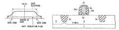
- FIGS. 1 and 2show a major structure of a semiconductor device manufactured in steps of a method of manufacturing the semiconductor device according to the first embodiment of the present invention.
- the intermediate structure of the semiconductor device shown in FIG. 1is formed in the following manner.
- element isolation regions 2 a and 2 bare formed in one surface of a semiconductor substrate 1 (for example, a silicon substrate).
- the element isolation regions 2 a and 2 bhave an STI (Shallow Trench Isolation) structure.
- element isolation regions of LOCOS (field oxide-film isolation) structuremay be formed in similar manner.
- P-type impuritiessuch as boron (B)
- P-type impuritiessuch as boron (B)
- P-type impuritiessuch as arsenic (As)
- PMOSFET-forming regionof the silicon substrate 1
- N-type impuritiessuch as arsenic (As)
- a gate insulating film 5is formed on the substrate 1 , covering the wells 3 and 4 .
- a polysilicon film 6is deposited on the gate insulating film 5 , to a thickness of, for example, 200 nm.
- a prescribed dielectric constant distributionis imparted to the gate insulting film 5 while the film 5 is being formed.
- the gate insulating film 5therefore has a higher dielectric constant in the side contacting the semiconductor substrate 1 than in the side contacting the gate electrode 6 a , as will be explained later.
- the polysilicon film 6is deposited, photolithography and etching processes are performed, both being of ordinary types.
- the film 6is thereby removed, except the part that lies between the element isolation regions 2 a and 2 b formed in the P well 3 , as is illustrated in FIG. 2 .
- This part of the film 6functions as the gate electrode 6 a of the NMOSFET.
- N-type impurity ionse.g., As ions
- P-type impurity ionse.g., B ions
- a shallow N-type source and drain regions 7are formed in the P well 3 for the NMOSFET region.
- the similar shallow source and drain regionsare formed in the P well 4 .
- a silicon nitride filmis deposited on the entire surface of the substrate 1 .
- RIEreactive Ion Etching
- N-type impurity ionse.g., As ions
- Source and drain diffusion layers 9 a and 9 bare thereby formed in the NMOSFET-forming region 3 .
- P-type impurity ionse.g., B ions
- Ti silicide films 10 a and 10 bare formed on the source diffusion layer 9 a and the drain diffusion layer 9 b , both provided in the N well 3 for forming the NMOSFET and a Ti silicide film 6 b is formed on the gate electrode 6 a , all by the method well known in the art.
- LPCVDLow-Pressure Chemical Vapor Deposition
- LPCVD oxide filmmade of SiO 2 to a thickness of about 900 nm on the entire surface of the structure.
- the LPCVD oxide filmis subjected to CMP (Chemical Mechanical Polishing) or the like and thereby made flat at the upper surface.
- CMPChemical Mechanical Polishing
- Contact holes 12 a and 12 bare made in the inter-layer insulating film 11 , exposing the prescribed surface portions of the Ti silicide films 10 a and 10 b that are provided on the source and drain diffusion layers 9 a and 9 b , respectively.
- a contact hole 12 cis made in the inter-layer insulating film 11 , too, reaching at a part of the Ti silicide film 6 b provided on the gate electrode 6 a .
- a metal-alloy wiring layere.g., Al—Si—Cu
- Ordinary photolithography and ordinary etchingare performed on the metal-alloy wiring layer to form wiring layers 13 a , 13 b and 13 c.
- a prescribed dielectric constant distributionis imparted to the gate insulating film 5 while the film 5 is being formed. That is, the film 5 is processed to have a higher dielectric constant in the side contacting the P well 3 formed in the substrate 1 than in the side contacting the gate electrode 6 a .
- the prescribed dielectric constant distributioncan be imparted to the gate insulating film 5 in various methods, which will be described below.
- silane gas and ammonia gasare applied to the substrate 1 held in a reaction furnace.
- a SiN filmis thereby formed on the entire surface of the substrate 1 , to a physical thickness of about 1.4 nm.
- Oxygenis then introduced into the SiN film by means of plasma oxidation to form the SiON film 5 .
- the plasma oxidationintroduces oxygen into the SiON film 5 , resulting in a specific oxygen distribution in the SiON film 5 .
- the SiON film 5has a high oxygen (O) distribution in the upper surface and a low oxygen distribution in the interface with the Si substrate 1 (i.e., the interface with the P well 3 or N well 4 ).
- the higher the oxygen contents of the SiON film 5the lower the dielectric constant of the SiN film 5 as shown in FIG. 3 .
- the dielectric constantis higher at the interface with the Si substrate 1 than in the upper surface of the film 5 .
- silane gasmay be replaced by a silane-based gas such as dichlorosilane.
- a Hf silicate ((HfO 2 ) x ((SiO 2 ) 1 ⁇ x , x ⁇ 1) filmis formed by MOCVD, as gate insulating film 5 , on the Si substrate ( FIG. 1 ) held in a reaction furnace (not shown).
- the ratio of the flow rates of a Hf-based feed gas (e.g., C 16 H 40 N 4 Hf), a Si-based feed gas (e.g., C 8 H 24 N 4 Si) and O 2is adjusted so that the flow rate of oxygen may increase with time.
- the gate insulating film 5 thus formedcan therefore contain much HfO 2 in the side contacting the Si substrate 1 and more SiO 2 than HfO 2 in the upper surface of the film 5 .
- the gate insulating film 5has a high dielectric constant at the interface with the P well 3 and a low dielectric constant in the side contacting the gate electrode 6 a .
- the feed gasesmay be replaced other similar gases.
- the HfO 2 concentrationcan be higher than the SiO 2 concentration in the side contacting the Si substrate 1 and the SiO 2 concentration can be higher than the HfO 2 concentration in the upper surface contacting the gate electrode 6 a if the temperature at which the film 5 is formed is decreased from 650° C. to 400° C. Therefore, when the film-forming temperature is so changed, instead of adjusting the ratio of the flow rates of the Hf-based feed gas, Si-based feed gas and O 2 , a desired dielectric constant distribution may also be realized.
- An Hf silicate filmis formed on the Si substrate 1 ( FIG. 1 ) by ALD method, by supplying Hf-based feed gas, Si-based feed gas and oxygen (O 2 ) into the reaction furnace, intermittently at such timings as shown in FIGS. 4A to 4C . More precisely, O2 is supplied for a longer period each time in a manner:(t 1 ⁇ t 2 ⁇ t 3 ⁇ t 4 ) as is shown in FIG. 4A , whereas the Hf-based feed gas and the Si-based feed gas are supplied for the same period each time as is illustrated in FIGS. 4B and 4C .
- the HfO 2 contentis higher than the SiO 2 content in the side of the gate insulating film 5 which contacts the Si substrate 1 , and the SiO 2 content is higher than the HfO 2 content in the upper surface of the film 5 contacting the gate electrode 6 a .
- the gate insulating film 5can have a high dielectric constant in the side contacting the Si substrate 1 and a low dielectric constant in the upper surface.
- the gate insulating film 5has a higher dielectric constant than SiO 2 in the side contacting the substrate 1 when the gate voltage is applied between the gate electrode 6 a and the source/drain regions 7 a and 7 b . Since the film 5 has a greater physical thickness than the conventional silicon oxide films, it can suppress the gate leakage current resulting from the direct tunneling current, though it has the same thickness as the conventional silicon oxide films.
- the lines of electric force, emanating from the gate electrode 6 ahardly pass through the edges of the gate insulating film 5 . This is because the film 5 has a small dielectric constant in the side that contacts the gate electrode 5 a . The lines of electric force therefore tend to concentrate at the center part of the gate insulating film 5 .
- the lines of electric forceexist in a high density at the center part of the film 5 and in a low density at the edges of the film 5 . Thus, no electric field concentration may occur at the edges of the gate electrode 6 a.
- the shallow source diffusion layer 7 a and the shallow drain diffusion layer 7 bhave their distal ends located more inside the channel than the edges of the gate electrode 6 a .
- the lines of electric forcetherefore may concentrate at the distal ends of the diffusion layers 7 a and 7 b . This mitigates the electric field concentration at the gate edge.
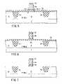
- This embodimentis identical to the first embodiment in terms of the basic structure of the MOSFET. It differs only in the distribution of dielectric constant in the gate insulating film. For simplicity, the components identical to those of the first embodiment are designated at the same reference numerals and will not be described in detail in the following description.
- a gate insulating filmfor example a Hf silicate film 5 a
- a gate insulating filmis formed to a prescribed thickness H 1 on the P well 3 (and also on N well 4 ), both formed in a surface of a Si substrate 1 .
- a polysilicon filmis deposited on the Hf silicate film 5 a .
- the polysilicon filmwill be processed to provide a gate electrode 6 a.
- a SiN filmis formed on the polysilicon film.
- the SiN filmis patterned by means of photolithography, forming a hard mask 21 .
- RIEis performed on the polysilicon film, patterning the polysilicon film and forming the gate electrode 6 a.
- the etching conditionis altered after the gate electrode 6 a is formed. All Hf silicate film 5 a , but the part lying beneath the gate electrode 6 a , is etched to about half (H ⁇ 1 ⁇ 2) the initial thickness. As a result, as shown in FIG. 5 , the sides of the Hf silicate film 5 a lying beneath the gate electrode 6 a are exposed at their upper halves, each having a height of about H1 ⁇ 2.
- SiH 4 gasis introduced into the reaction furnace, along with diluting gas such as He.
- diluting gassuch as He.
- electrical dischargingis effected, thus generating Si plasma.
- Silicon (Si)is thereby introduced into the Hf silicate film 5 a.
- Siis introduced not only into the Hf silicate film 5 a , but also into the gate electrode 6 a made of polysilicon and the hard mask made of SiN as is illustrated in FIG. 6 .
- broken lines 22 in FIG. 6indicate the parts of the Hf silicate film 5 a , electrode 6 a and hard mask, into which Si has been introduced. That part of the Hf silicate film 6 a , which lies beneath the gate electrode 6 a , is thicker than any other part. Therefore, Si is introduced into the sides of the part of the film 5 a beneath the gate electrode 6 a , but not into the center part thereof. It follows that the Si concentration is high in the sides of said part of the Hf silicate film 5 a and is low in the center part thereof, in the channel length direction.
- the Si concentrationis high in the edges of the gate insulating film 5 a (that is, Hf/Si ratio is small) and is low in the center wide part of the film 5 a (that is, Hf/Si ratio is large).
- the gate insulating film 5 acan therefore have a high dielectric constant in the center wide part and a low dielectric constant in the edges.
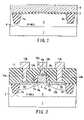
- gate insulation film 23is deposited on the whole surface of the substrate 1 as shown in FIG. 9 followed by an etching process to leave gate side-walls 23 a and 23 b on the sides of the gate electrode 6 a as is shown in FIG. 10 .
- the Hf silicate film 5 amay be removed, but the parts that lie beneath the gate sidewalls 23 a and 23 b , may be left as is illustrated in FIG. 10 .
- Another methodmay be used to lower the dielectric constant of the edges of the gate insulating film 5 a .
- Al plasma, not Siis introduced into the edges of the gate insulating film in the step explained with reference to FIG. 6 .
- the edgesmay be exposed to Si radical or Al radical at 400° C. or more, instead of being exposed to plasma.
- the lines of electric forcebecome dense at the center part of the gate insulating film 5 a and sparse at the edges of the film 5 a in the channel length direction when the gate voltage is applied between the gate electrode 6 a and the source/drain regions 7 a and 7 b .
- the electric fieldis distributed to be intense at the center part of the gate insulating film 5 a . The electric field can therefore be prevented from concentrating at the edges of the gate electrode 6 a.
- the concentration of an electric field at the gate edge of a MOSFETcan be mitigated without rounding the gate electrode edge by oxidation, even if the gate insulating film is formed by materials which cannot make the gate edge rounded by the oxidation due to the limited thermal stability and resistance to oxidation of the gate insulating film.
Landscapes
- Chemical & Material Sciences (AREA)
- Engineering & Computer Science (AREA)
- General Chemical & Material Sciences (AREA)
- Chemical Kinetics & Catalysis (AREA)
- General Physics & Mathematics (AREA)
- Computer Hardware Design (AREA)
- Metallurgy (AREA)
- Organic Chemistry (AREA)
- Power Engineering (AREA)
- Crystallography & Structural Chemistry (AREA)
- Physics & Mathematics (AREA)
- Condensed Matter Physics & Semiconductors (AREA)
- Materials Engineering (AREA)
- Manufacturing & Machinery (AREA)
- Mechanical Engineering (AREA)
- Microelectronics & Electronic Packaging (AREA)
- Inorganic Chemistry (AREA)
- Insulated Gate Type Field-Effect Transistor (AREA)
- Formation Of Insulating Films (AREA)
Abstract
Description
εdiele(sub)>εdiele(elec)
where ε diele(sub) is the dielectric constant of the
εdiele(center)>εdiele(edge)
where ε diele(center) is the dielectric constant the
<Second embodiment wherein dielectric constant varies along the channel in the channel length direction>
Claims (4)
Priority Applications (1)
| Application Number | Priority Date | Filing Date | Title |
|---|---|---|---|
| US11/193,349US7396748B2 (en) | 2001-03-28 | 2005-08-01 | Semiconductor device includes gate insulating film having a high dielectric constant |
Applications Claiming Priority (7)
| Application Number | Priority Date | Filing Date | Title |
|---|---|---|---|
| JP2001-092531 | 2001-03-28 | ||
| JP2001092531 | 2001-03-28 | ||
| JP2002-083380 | 2002-03-25 | ||
| JP2002083380AJP4184686B2 (en) | 2001-03-28 | 2002-03-25 | Manufacturing method of semiconductor device |
| US10/106,345US6664577B2 (en) | 2001-03-28 | 2002-03-27 | Semiconductor device includes gate insulating film having a high dielectric constant |
| US10/680,163US6949425B2 (en) | 2001-03-28 | 2003-10-08 | Semiconductor device includes gate insulating film having a high dielectric constant |
| US11/193,349US7396748B2 (en) | 2001-03-28 | 2005-08-01 | Semiconductor device includes gate insulating film having a high dielectric constant |
Related Parent Applications (1)
| Application Number | Title | Priority Date | Filing Date |
|---|---|---|---|
| US10/680,163DivisionUS6949425B2 (en) | 2001-03-28 | 2003-10-08 | Semiconductor device includes gate insulating film having a high dielectric constant |
Publications (2)
| Publication Number | Publication Date |
|---|---|
| US20050263803A1 US20050263803A1 (en) | 2005-12-01 |
| US7396748B2true US7396748B2 (en) | 2008-07-08 |
Family
ID=26612349
Family Applications (3)
| Application Number | Title | Priority Date | Filing Date |
|---|---|---|---|
| US10/106,345Expired - LifetimeUS6664577B2 (en) | 2001-03-28 | 2002-03-27 | Semiconductor device includes gate insulating film having a high dielectric constant |
| US10/680,163Expired - LifetimeUS6949425B2 (en) | 2001-03-28 | 2003-10-08 | Semiconductor device includes gate insulating film having a high dielectric constant |
| US11/193,349Expired - LifetimeUS7396748B2 (en) | 2001-03-28 | 2005-08-01 | Semiconductor device includes gate insulating film having a high dielectric constant |
Family Applications Before (2)
| Application Number | Title | Priority Date | Filing Date |
|---|---|---|---|
| US10/106,345Expired - LifetimeUS6664577B2 (en) | 2001-03-28 | 2002-03-27 | Semiconductor device includes gate insulating film having a high dielectric constant |
| US10/680,163Expired - LifetimeUS6949425B2 (en) | 2001-03-28 | 2003-10-08 | Semiconductor device includes gate insulating film having a high dielectric constant |
Country Status (2)
| Country | Link |
|---|---|
| US (3) | US6664577B2 (en) |
| JP (1) | JP4184686B2 (en) |
Cited By (1)
| Publication number | Priority date | Publication date | Assignee | Title |
|---|---|---|---|---|
| US20100297809A1 (en)* | 2005-04-25 | 2010-11-25 | Semiconductor Energy Laboratory Co., Ltd. | Organic transistor, manufacturing method of semiconductor device and organic transistor |
Families Citing this family (16)
| Publication number | Priority date | Publication date | Assignee | Title |
|---|---|---|---|---|
| US9139906B2 (en) | 2001-03-06 | 2015-09-22 | Asm America, Inc. | Doping with ALD technology |
| EP1256638B1 (en)* | 2001-05-07 | 2008-03-26 | Samsung Electronics Co., Ltd. | Method of forming a multi-components thin film |
| JP4120938B2 (en)* | 2001-08-23 | 2008-07-16 | 日本電気株式会社 | Semiconductor device having high dielectric constant insulating film and manufacturing method thereof |
| KR100514172B1 (en)* | 2004-01-19 | 2005-09-09 | 삼성전자주식회사 | Method of forming semiconductor device |
| JP4526995B2 (en)* | 2004-04-09 | 2010-08-18 | 東京エレクトロン株式会社 | Method for forming gate insulating film, computer-readable storage medium, and computer program |
| KR100688521B1 (en)* | 2005-01-18 | 2007-03-02 | 삼성전자주식회사 | Semiconductor device including high dielectric constant insulating film and manufacturing method thereof |
| US20060156980A1 (en) | 2005-01-19 | 2006-07-20 | Samsung Electronics Co., Ltd. | Apparatus including 4-way valve for fabricating semiconductor device, method of controlling valve, and method of fabricating semiconductor device using the apparatus |
| US7504700B2 (en)* | 2005-04-21 | 2009-03-17 | International Business Machines Corporation | Method of forming an ultra-thin [[HfSiO]] metal silicate film for high performance CMOS applications and semiconductor structure formed in said method |
| JP2006332614A (en)* | 2005-04-25 | 2006-12-07 | Semiconductor Energy Lab Co Ltd | Semiconductor device, organic transistor and manufacturing method thereof |
| US7351632B2 (en)* | 2005-04-29 | 2008-04-01 | Texas Instruments Incorporated | Semiconductor CMOS devices and methods with NMOS high-k dielectric formed prior to core PMOS silicon oxynitride dielectric formation using direct nitridation of silicon |
| US8218283B2 (en)* | 2005-07-15 | 2012-07-10 | Telefonaktiebolaget L M Ericsson (Publ) | Resistive films for electrode peak-field suppression |
| JP5126930B2 (en)* | 2006-02-06 | 2013-01-23 | ルネサスエレクトロニクス株式会社 | Manufacturing method of semiconductor device |
| JP2008053683A (en)* | 2006-07-27 | 2008-03-06 | Matsushita Electric Ind Co Ltd | Insulating film forming method, semiconductor device, and substrate processing apparatus |
| WO2008042981A2 (en)* | 2006-10-05 | 2008-04-10 | Asm America, Inc. | Ald of metal silicate films |
| JP2009295621A (en)* | 2008-06-02 | 2009-12-17 | Panasonic Corp | Semiconductor device and method of manufacturing the same |
| US10147823B2 (en)* | 2015-03-19 | 2018-12-04 | Semiconductor Energy Laboratory Co., Ltd. | Semiconductor device |
Citations (15)
| Publication number | Priority date | Publication date | Assignee | Title |
|---|---|---|---|---|
| JPH11135774A (en) | 1997-07-24 | 1999-05-21 | Texas Instr Inc <Ti> | High dielectric constant silicate gate dielectric |
| JP2000003885A (en) | 1998-04-15 | 2000-01-07 | Lucent Technol Inc | Method of manufacturing field effect devices and capacitors using improved thin film dielectrics and resulting devices |
| US6013553A (en) | 1997-07-24 | 2000-01-11 | Texas Instruments Incorporated | Zirconium and/or hafnium oxynitride gate dielectric |
| WO2000049643A2 (en) | 1999-02-16 | 2000-08-24 | Koninklijke Philips Electronics N.V. | Gate insulator comprising high and low dielectric constant parts |
| JP2001024188A (en) | 1999-07-07 | 2001-01-26 | Nec Corp | Semiconductor device and its manufacture |
| US6225669B1 (en)* | 1998-09-30 | 2001-05-01 | Advanced Micro Devices, Inc. | Non-uniform gate/dielectric field effect transistor |
| US6303481B2 (en) | 1999-12-29 | 2001-10-16 | Hyundai Electronics Industries Co., Ltd. | Method for forming a gate insulating film for semiconductor devices |
| US20020047141A1 (en) | 2000-09-07 | 2002-04-25 | Mitsubishi Denki Kabushiki Kaisha | Semiconductor device, and manufacture thereof |
| JP2002203958A (en) | 2000-12-28 | 2002-07-19 | Toshiba Corp | Semiconductor device and manufacturing method thereof |
| US6576967B1 (en) | 2000-09-18 | 2003-06-10 | Motorola, Inc. | Semiconductor structure and process for forming a metal oxy-nitride dielectric layer |
| JP2003234471A (en) | 2002-02-07 | 2003-08-22 | Toshiba Corp | Semiconductor device and manufacturing method thereof |
| US6841439B1 (en)* | 1997-07-24 | 2005-01-11 | Texas Instruments Incorporated | High permittivity silicate gate dielectric |
| US6924536B2 (en)* | 2002-02-26 | 2005-08-02 | Kabushiki Kaisha Toshiba | Semiconductor device and its manufacturing method |
| US7034369B2 (en)* | 2003-08-29 | 2006-04-25 | Kabushiki Kaisha Toshiba | Semiconductor device and method for manufacturing the same |
| US7161203B2 (en)* | 2004-06-04 | 2007-01-09 | Micron Technology, Inc. | Gated field effect device comprising gate dielectric having different K regions |
Family Cites Families (1)
| Publication number | Priority date | Publication date | Assignee | Title |
|---|---|---|---|---|
| KR20000018524A (en)* | 1998-09-02 | 2000-04-06 | 김영환 | Non volatile memory device and a manufacturing method thereof |
- 2002
- 2002-03-25JPJP2002083380Apatent/JP4184686B2/ennot_activeExpired - Lifetime
- 2002-03-27USUS10/106,345patent/US6664577B2/ennot_activeExpired - Lifetime
- 2003
- 2003-10-08USUS10/680,163patent/US6949425B2/ennot_activeExpired - Lifetime
- 2005
- 2005-08-01USUS11/193,349patent/US7396748B2/ennot_activeExpired - Lifetime
Patent Citations (15)
| Publication number | Priority date | Publication date | Assignee | Title |
|---|---|---|---|---|
| US6841439B1 (en)* | 1997-07-24 | 2005-01-11 | Texas Instruments Incorporated | High permittivity silicate gate dielectric |
| US6013553A (en) | 1997-07-24 | 2000-01-11 | Texas Instruments Incorporated | Zirconium and/or hafnium oxynitride gate dielectric |
| JPH11135774A (en) | 1997-07-24 | 1999-05-21 | Texas Instr Inc <Ti> | High dielectric constant silicate gate dielectric |
| JP2000003885A (en) | 1998-04-15 | 2000-01-07 | Lucent Technol Inc | Method of manufacturing field effect devices and capacitors using improved thin film dielectrics and resulting devices |
| US6225669B1 (en)* | 1998-09-30 | 2001-05-01 | Advanced Micro Devices, Inc. | Non-uniform gate/dielectric field effect transistor |
| WO2000049643A2 (en) | 1999-02-16 | 2000-08-24 | Koninklijke Philips Electronics N.V. | Gate insulator comprising high and low dielectric constant parts |
| JP2001024188A (en) | 1999-07-07 | 2001-01-26 | Nec Corp | Semiconductor device and its manufacture |
| US6303481B2 (en) | 1999-12-29 | 2001-10-16 | Hyundai Electronics Industries Co., Ltd. | Method for forming a gate insulating film for semiconductor devices |
| US20020047141A1 (en) | 2000-09-07 | 2002-04-25 | Mitsubishi Denki Kabushiki Kaisha | Semiconductor device, and manufacture thereof |
| US6576967B1 (en) | 2000-09-18 | 2003-06-10 | Motorola, Inc. | Semiconductor structure and process for forming a metal oxy-nitride dielectric layer |
| JP2002203958A (en) | 2000-12-28 | 2002-07-19 | Toshiba Corp | Semiconductor device and manufacturing method thereof |
| JP2003234471A (en) | 2002-02-07 | 2003-08-22 | Toshiba Corp | Semiconductor device and manufacturing method thereof |
| US6924536B2 (en)* | 2002-02-26 | 2005-08-02 | Kabushiki Kaisha Toshiba | Semiconductor device and its manufacturing method |
| US7034369B2 (en)* | 2003-08-29 | 2006-04-25 | Kabushiki Kaisha Toshiba | Semiconductor device and method for manufacturing the same |
| US7161203B2 (en)* | 2004-06-04 | 2007-01-09 | Micron Technology, Inc. | Gated field effect device comprising gate dielectric having different K regions |
Non-Patent Citations (1)
| Title |
|---|
| Yudong Kim, et al. "Conventional n-channel MOSFET devices using single layer HfO<SUB>2 </SUB>and ZrO<SUB>2 </SUB>as high-k gate dielectrics with polysilicon gate electrode", IEDM, 01-455, pp. 455-458, Dec. 2, 2001. |
Cited By (3)
| Publication number | Priority date | Publication date | Assignee | Title |
|---|---|---|---|---|
| US20100297809A1 (en)* | 2005-04-25 | 2010-11-25 | Semiconductor Energy Laboratory Co., Ltd. | Organic transistor, manufacturing method of semiconductor device and organic transistor |
| US8343816B2 (en) | 2005-04-25 | 2013-01-01 | Semiconductor Energy Laboratory Co., Ltd. | Organic transistor, manufacturing method of semiconductor device and organic transistor |
| US8785259B2 (en) | 2005-04-25 | 2014-07-22 | Semiconductor Energy Laboratory Co., Ltd. | Organic transistor, manufacturing method of semiconductor device and organic transistor |
Also Published As
| Publication number | Publication date |
|---|---|
| US20040070037A1 (en) | 2004-04-15 |
| US6949425B2 (en) | 2005-09-27 |
| US20050263803A1 (en) | 2005-12-01 |
| US6664577B2 (en) | 2003-12-16 |
| JP2002359371A (en) | 2002-12-13 |
| US20020140098A1 (en) | 2002-10-03 |
| JP4184686B2 (en) | 2008-11-19 |
Similar Documents
| Publication | Publication Date | Title |
|---|---|---|
| US11848369B2 (en) | Horizontal gate-all-around device nanowire air gap spacer formation | |
| US7396748B2 (en) | Semiconductor device includes gate insulating film having a high dielectric constant | |
| KR100817949B1 (en) | Nonplanar device with stress incorporation layer and method of fabrication | |
| KR100563748B1 (en) | Manufacturing method of semiconductor device | |
| US7456476B2 (en) | Nonplanar semiconductor device with partially or fully wrapped around gate electrode and methods of fabrication | |
| US7947591B2 (en) | Semiconductor devices with dual-metal gate structures and fabrication methods thereof | |
| US11791398B2 (en) | Nano multilayer carbon-rich low-k spacer | |
| US20060024879A1 (en) | Selectively strained MOSFETs to improve drive current | |
| JP2009088440A (en) | Semiconductor device and manufacturing method thereof | |
| KR100687153B1 (en) | Semiconductor device and manufacturing method thereof | |
| US5093700A (en) | Single gate structure with oxide layer therein | |
| JPH0752772B2 (en) | Manufacturing method of semiconductor device | |
| CN109585565A (en) | Semiconductor devices and its manufacturing method | |
| JP2004172178A (en) | Semiconductor device and method of manufacturing semiconductor device | |
| JP2671607B2 (en) | Semiconductor device and manufacturing method thereof | |
| GB2318451A (en) | Fabricating a semiconductor device | |
| US20020175327A1 (en) | Arrangement with a semiconductor component | |
| JP3487541B2 (en) | Method for manufacturing field effect transistor | |
| CN113823597A (en) | Method of manufacturing semiconductor device | |
| KR100269604B1 (en) | Method of manufacturing thin film transistor of semiconductor device | |
| EP0434383B1 (en) | Semiconductor device gate structure with oxide layer therein | |
| US20050121738A1 (en) | Contact etch resistant spacers | |
| JP2006156568A (en) | Semiconductor device |
Legal Events
| Date | Code | Title | Description |
|---|---|---|---|
| STCF | Information on status: patent grant | Free format text:PATENTED CASE | |
| FPAY | Fee payment | Year of fee payment:4 | |
| FPAY | Fee payment | Year of fee payment:8 | |
| AS | Assignment | Owner name:TOSHIBA MEMORY CORPORATION, JAPAN Free format text:ASSIGNMENT OF ASSIGNORS INTEREST;ASSIGNOR:KABUSHIKI KAISHA TOSHIBA;REEL/FRAME:043709/0035 Effective date:20170706 | |
| MAFP | Maintenance fee payment | Free format text:PAYMENT OF MAINTENANCE FEE, 12TH YEAR, LARGE ENTITY (ORIGINAL EVENT CODE: M1553); ENTITY STATUS OF PATENT OWNER: LARGE ENTITY Year of fee payment:12 | |
| AS | Assignment | Owner name:K.K. PANGEA, JAPAN Free format text:MERGER;ASSIGNOR:TOSHIBA MEMORY CORPORATION;REEL/FRAME:055659/0471 Effective date:20180801 Owner name:TOSHIBA MEMORY CORPORATION, JAPAN Free format text:CHANGE OF NAME AND ADDRESS;ASSIGNOR:K.K. PANGEA;REEL/FRAME:055669/0401 Effective date:20180801 Owner name:KIOXIA CORPORATION, JAPAN Free format text:CHANGE OF NAME AND ADDRESS;ASSIGNOR:TOSHIBA MEMORY CORPORATION;REEL/FRAME:055669/0001 Effective date:20191001 |