US7396475B2 - Method of forming stepped structures employing imprint lithography - Google Patents
Method of forming stepped structures employing imprint lithographyDownload PDFInfo
- Publication number
- US7396475B2 US7396475B2US10/423,642US42364203AUS7396475B2US 7396475 B2US7396475 B2US 7396475B2US 42364203 AUS42364203 AUS 42364203AUS 7396475 B2US7396475 B2US 7396475B2
- Authority
- US
- United States
- Prior art keywords
- substrate
- forming
- layer
- recited
- etch selectivity
- Prior art date
- Legal status (The legal status is an assumption and is not a legal conclusion. Google has not performed a legal analysis and makes no representation as to the accuracy of the status listed.)
- Expired - Lifetime, expires
Links
- 238000000034methodMethods0.000titleclaimsabstractdescription60
- 238000001459lithographyMethods0.000titledescription3
- 239000000758substrateSubstances0.000claimsabstractdescription81
- 239000000463materialSubstances0.000claimsdescription63
- 230000005855radiationEffects0.000claimsdescription19
- XUIMIQQOPSSXEZ-UHFFFAOYSA-NSiliconChemical compound[Si]XUIMIQQOPSSXEZ-UHFFFAOYSA-N0.000claimsdescription16
- 229910052710siliconInorganic materials0.000claimsdescription16
- 239000010703siliconSubstances0.000claimsdescription16
- 239000000203mixtureSubstances0.000claimsdescription13
- 150000001875compoundsChemical class0.000claimsdescription10
- 238000000151depositionMethods0.000claimsdescription9
- 239000004094surface-active agentSubstances0.000claimsdescription8
- 239000004020conductorSubstances0.000claimsdescription7
- 230000000295complement effectEffects0.000claimsdescription6
- 239000012530fluidSubstances0.000claimsdescription4
- 238000004528spin coatingMethods0.000claims2
- 230000008569processEffects0.000description23
- 238000004519manufacturing processMethods0.000description12
- 230000015572biosynthetic processEffects0.000description8
- QVGXLLKOCUKJST-UHFFFAOYSA-Natomic oxygenChemical compound[O]QVGXLLKOCUKJST-UHFFFAOYSA-N0.000description7
- 239000001301oxygenSubstances0.000description7
- 229910052760oxygenInorganic materials0.000description7
- 239000011324beadSubstances0.000description6
- 238000010606normalizationMethods0.000description6
- 230000004888barrier functionEffects0.000description5
- 238000000576coating methodMethods0.000description5
- 238000005530etchingMethods0.000description5
- YCKRFDGAMUMZLT-UHFFFAOYSA-NFluorine atomChemical compound[F]YCKRFDGAMUMZLT-UHFFFAOYSA-N0.000description4
- 239000011248coating agentSubstances0.000description4
- 230000009969flowable effectEffects0.000description4
- 239000011737fluorineSubstances0.000description4
- 229910052731fluorineInorganic materials0.000description4
- 239000007789gasSubstances0.000description4
- VYPSYNLAJGMNEJ-UHFFFAOYSA-NSilicium dioxideChemical compoundO=[Si]=OVYPSYNLAJGMNEJ-UHFFFAOYSA-N0.000description3
- 230000008901benefitEffects0.000description3
- 238000005229chemical vapour depositionMethods0.000description3
- 229920006037cross link polymerPolymers0.000description3
- 230000008021depositionEffects0.000description3
- 230000009977dual effectEffects0.000description3
- 229910052751metalInorganic materials0.000description3
- 239000002184metalSubstances0.000description3
- 238000001393microlithographyMethods0.000description3
- 238000005240physical vapour depositionMethods0.000description3
- 239000002861polymer materialSubstances0.000description3
- 239000004065semiconductorSubstances0.000description3
- 238000001494step-and-flash imprint lithographyMethods0.000description3
- KUDUQBURMYMBIJ-UHFFFAOYSA-N2-prop-2-enoyloxyethyl prop-2-enoateChemical compoundC=CC(=O)OCCOC(=O)C=CKUDUQBURMYMBIJ-UHFFFAOYSA-N0.000description2
- RYGMFSIKBFXOCR-UHFFFAOYSA-NCopperChemical compound[Cu]RYGMFSIKBFXOCR-UHFFFAOYSA-N0.000description2
- 229910052770UraniumInorganic materials0.000description2
- 229910052782aluminiumInorganic materials0.000description2
- XAGFODPZIPBFFR-UHFFFAOYSA-NaluminiumChemical compound[Al]XAGFODPZIPBFFR-UHFFFAOYSA-N0.000description2
- 239000000919ceramicSubstances0.000description2
- 229910052802copperInorganic materials0.000description2
- 239000010949copperSubstances0.000description2
- 238000005137deposition processMethods0.000description2
- 239000005350fused silica glassSubstances0.000description2
- 239000011810insulating materialSubstances0.000description2
- 238000002348laser-assisted direct imprint lithographyMethods0.000description2
- 239000000178monomerSubstances0.000description2
- 150000003254radicalsChemical class0.000description2
- 229910052721tungstenInorganic materials0.000description2
- 239000010937tungstenSubstances0.000description2
- 206010073306Exposure to radiationDiseases0.000description1
- 229910000640Fe alloyInorganic materials0.000description1
- 229910001374InvarInorganic materials0.000description1
- RTAQQCXQSZGOHL-UHFFFAOYSA-NTitaniumChemical compound[Ti]RTAQQCXQSZGOHL-UHFFFAOYSA-N0.000description1
- NRTOMJZYCJJWKI-UHFFFAOYSA-NTitanium nitrideChemical compound[Ti]#NNRTOMJZYCJJWKI-UHFFFAOYSA-N0.000description1
- 239000006094ZerodurSubstances0.000description1
- 238000000231atomic layer depositionMethods0.000description1
- 230000009286beneficial effectEffects0.000description1
- 239000005388borosilicate glassSubstances0.000description1
- 238000005219brazingMethods0.000description1
- CQEYYJKEWSMYFG-UHFFFAOYSA-Nbutyl acrylateChemical compoundCCCCOC(=O)C=CCQEYYJKEWSMYFG-UHFFFAOYSA-N0.000description1
- 238000004140cleaningMethods0.000description1
- 238000010276constructionMethods0.000description1
- 239000003431cross linking reagentSubstances0.000description1
- KBLWLMPSVYBVDK-UHFFFAOYSA-Ncyclohexyl prop-2-enoateChemical compoundC=CC(=O)OC1CCCCC1KBLWLMPSVYBVDK-UHFFFAOYSA-N0.000description1
- 230000001419dependent effectEffects0.000description1
- 239000003989dielectric materialSubstances0.000description1
- KPUWHANPEXNPJT-UHFFFAOYSA-NdisiloxaneChemical class[SiH3]O[SiH3]KPUWHANPEXNPJT-UHFFFAOYSA-N0.000description1
- 238000004049embossingMethods0.000description1
- 229920002313fluoropolymerPolymers0.000description1
- 239000011521glassSubstances0.000description1
- 230000006872improvementEffects0.000description1
- 238000011065in-situ storageMethods0.000description1
- 230000003993interactionEffects0.000description1
- 238000004377microelectronicMethods0.000description1
- 230000004048modificationEffects0.000description1
- 238000012986modificationMethods0.000description1
- 238000001127nanoimprint lithographyMethods0.000description1
- 239000002086nanomaterialSubstances0.000description1
- 239000011368organic materialSubstances0.000description1
- 229920000620organic polymerPolymers0.000description1
- 125000001181organosilyl groupChemical group[SiH3]*0.000description1
- 238000000059patterningMethods0.000description1
- 229920000642polymerPolymers0.000description1
- 238000006116polymerization reactionMethods0.000description1
- 238000004886process controlMethods0.000description1
- 239000010453quartzSubstances0.000description1
- 230000009467reductionEffects0.000description1
- HBMJWWWQQXIZIP-UHFFFAOYSA-Nsilicon carbideChemical compound[Si+]#[C-]HBMJWWWQQXIZIP-UHFFFAOYSA-N0.000description1
- 229910010271silicon carbideInorganic materials0.000description1
- GRJISGHXMUQUMC-UHFFFAOYSA-Nsilyl prop-2-enoateChemical compound[SiH3]OC(=O)C=CGRJISGHXMUQUMC-UHFFFAOYSA-N0.000description1
- 239000007787solidSubstances0.000description1
- 230000007480spreadingEffects0.000description1
- 238000003892spreadingMethods0.000description1
- 238000004544sputter depositionMethods0.000description1
- 239000010936titaniumSubstances0.000description1
- 229910052719titaniumInorganic materials0.000description1
- WFKWXMTUELFFGS-UHFFFAOYSA-NtungstenChemical compound[W]WFKWXMTUELFFGS-UHFFFAOYSA-N0.000description1
Images


Classifications
- G—PHYSICS
- G03—PHOTOGRAPHY; CINEMATOGRAPHY; ANALOGOUS TECHNIQUES USING WAVES OTHER THAN OPTICAL WAVES; ELECTROGRAPHY; HOLOGRAPHY
- G03F—PHOTOMECHANICAL PRODUCTION OF TEXTURED OR PATTERNED SURFACES, e.g. FOR PRINTING, FOR PROCESSING OF SEMICONDUCTOR DEVICES; MATERIALS THEREFOR; ORIGINALS THEREFOR; APPARATUS SPECIALLY ADAPTED THEREFOR
- G03F7/00—Photomechanical, e.g. photolithographic, production of textured or patterned surfaces, e.g. printing surfaces; Materials therefor, e.g. comprising photoresists; Apparatus specially adapted therefor
- B—PERFORMING OPERATIONS; TRANSPORTING
- B81—MICROSTRUCTURAL TECHNOLOGY
- B81C—PROCESSES OR APPARATUS SPECIALLY ADAPTED FOR THE MANUFACTURE OR TREATMENT OF MICROSTRUCTURAL DEVICES OR SYSTEMS
- B81C1/00—Manufacture or treatment of devices or systems in or on a substrate
- B81C1/00436—Shaping materials, i.e. techniques for structuring the substrate or the layers on the substrate
- B81C1/00444—Surface micromachining, i.e. structuring layers on the substrate
- B81C1/0046—Surface micromachining, i.e. structuring layers on the substrate using stamping, e.g. imprinting
- B—PERFORMING OPERATIONS; TRANSPORTING
- B44—DECORATIVE ARTS
- B44C—PRODUCING DECORATIVE EFFECTS; MOSAICS; TARSIA WORK; PAPERHANGING
- B44C1/00—Processes, not specifically provided for elsewhere, for producing decorative surface effects
- B44C1/22—Removing surface-material, e.g. by engraving, by etching
- B—PERFORMING OPERATIONS; TRANSPORTING
- B82—NANOTECHNOLOGY
- B82Y—SPECIFIC USES OR APPLICATIONS OF NANOSTRUCTURES; MEASUREMENT OR ANALYSIS OF NANOSTRUCTURES; MANUFACTURE OR TREATMENT OF NANOSTRUCTURES
- B82Y10/00—Nanotechnology for information processing, storage or transmission, e.g. quantum computing or single electron logic
- B—PERFORMING OPERATIONS; TRANSPORTING
- B82—NANOTECHNOLOGY
- B82Y—SPECIFIC USES OR APPLICATIONS OF NANOSTRUCTURES; MEASUREMENT OR ANALYSIS OF NANOSTRUCTURES; MANUFACTURE OR TREATMENT OF NANOSTRUCTURES
- B82Y40/00—Manufacture or treatment of nanostructures
- C—CHEMISTRY; METALLURGY
- C03—GLASS; MINERAL OR SLAG WOOL
- C03C—CHEMICAL COMPOSITION OF GLASSES, GLAZES OR VITREOUS ENAMELS; SURFACE TREATMENT OF GLASS; SURFACE TREATMENT OF FIBRES OR FILAMENTS MADE FROM GLASS, MINERALS OR SLAGS; JOINING GLASS TO GLASS OR OTHER MATERIALS
- C03C17/00—Surface treatment of glass, not in the form of fibres or filaments, by coating
- C03C17/001—General methods for coating; Devices therefor
- C03C17/002—General methods for coating; Devices therefor for flat glass, e.g. float glass
- C—CHEMISTRY; METALLURGY
- C03—GLASS; MINERAL OR SLAG WOOL
- C03C—CHEMICAL COMPOSITION OF GLASSES, GLAZES OR VITREOUS ENAMELS; SURFACE TREATMENT OF GLASS; SURFACE TREATMENT OF FIBRES OR FILAMENTS MADE FROM GLASS, MINERALS OR SLAGS; JOINING GLASS TO GLASS OR OTHER MATERIALS
- C03C23/00—Other surface treatment of glass not in the form of fibres or filaments
- C03C23/0005—Other surface treatment of glass not in the form of fibres or filaments by irradiation
- C03C23/002—Other surface treatment of glass not in the form of fibres or filaments by irradiation by ultraviolet light
- C—CHEMISTRY; METALLURGY
- C23—COATING METALLIC MATERIAL; COATING MATERIAL WITH METALLIC MATERIAL; CHEMICAL SURFACE TREATMENT; DIFFUSION TREATMENT OF METALLIC MATERIAL; COATING BY VACUUM EVAPORATION, BY SPUTTERING, BY ION IMPLANTATION OR BY CHEMICAL VAPOUR DEPOSITION, IN GENERAL; INHIBITING CORROSION OF METALLIC MATERIAL OR INCRUSTATION IN GENERAL
- C23F—NON-MECHANICAL REMOVAL OF METALLIC MATERIAL FROM SURFACE; INHIBITING CORROSION OF METALLIC MATERIAL OR INCRUSTATION IN GENERAL; MULTI-STEP PROCESSES FOR SURFACE TREATMENT OF METALLIC MATERIAL INVOLVING AT LEAST ONE PROCESS PROVIDED FOR IN CLASS C23 AND AT LEAST ONE PROCESS COVERED BY SUBCLASS C21D OR C22F OR CLASS C25
- C23F1/00—Etching metallic material by chemical means
- G—PHYSICS
- G03—PHOTOGRAPHY; CINEMATOGRAPHY; ANALOGOUS TECHNIQUES USING WAVES OTHER THAN OPTICAL WAVES; ELECTROGRAPHY; HOLOGRAPHY
- G03F—PHOTOMECHANICAL PRODUCTION OF TEXTURED OR PATTERNED SURFACES, e.g. FOR PRINTING, FOR PROCESSING OF SEMICONDUCTOR DEVICES; MATERIALS THEREFOR; ORIGINALS THEREFOR; APPARATUS SPECIALLY ADAPTED THEREFOR
- G03F7/00—Photomechanical, e.g. photolithographic, production of textured or patterned surfaces, e.g. printing surfaces; Materials therefor, e.g. comprising photoresists; Apparatus specially adapted therefor
- G03F7/0002—Lithographic processes using patterning methods other than those involving the exposure to radiation, e.g. by stamping
- H—ELECTRICITY
- H01—ELECTRIC ELEMENTS
- H01L—SEMICONDUCTOR DEVICES NOT COVERED BY CLASS H10
- H01L21/00—Processes or apparatus adapted for the manufacture or treatment of semiconductor or solid state devices or of parts thereof
- H01L21/70—Manufacture or treatment of devices consisting of a plurality of solid state components formed in or on a common substrate or of parts thereof; Manufacture of integrated circuit devices or of parts thereof
- H01L21/71—Manufacture of specific parts of devices defined in group H01L21/70
- H01L21/768—Applying interconnections to be used for carrying current between separate components within a device comprising conductors and dielectrics
- H01L21/76801—Applying interconnections to be used for carrying current between separate components within a device comprising conductors and dielectrics characterised by the formation and the after-treatment of the dielectrics, e.g. smoothing
- H01L21/76802—Applying interconnections to be used for carrying current between separate components within a device comprising conductors and dielectrics characterised by the formation and the after-treatment of the dielectrics, e.g. smoothing by forming openings in dielectrics
- H01L21/76807—Applying interconnections to be used for carrying current between separate components within a device comprising conductors and dielectrics characterised by the formation and the after-treatment of the dielectrics, e.g. smoothing by forming openings in dielectrics for dual damascene structures
- H01L21/76813—Applying interconnections to be used for carrying current between separate components within a device comprising conductors and dielectrics characterised by the formation and the after-treatment of the dielectrics, e.g. smoothing by forming openings in dielectrics for dual damascene structures involving a partial via etch
- H—ELECTRICITY
- H01—ELECTRIC ELEMENTS
- H01L—SEMICONDUCTOR DEVICES NOT COVERED BY CLASS H10
- H01L21/00—Processes or apparatus adapted for the manufacture or treatment of semiconductor or solid state devices or of parts thereof
- H01L21/70—Manufacture or treatment of devices consisting of a plurality of solid state components formed in or on a common substrate or of parts thereof; Manufacture of integrated circuit devices or of parts thereof
- H01L21/71—Manufacture of specific parts of devices defined in group H01L21/70
- H01L21/768—Applying interconnections to be used for carrying current between separate components within a device comprising conductors and dielectrics
- H01L21/76801—Applying interconnections to be used for carrying current between separate components within a device comprising conductors and dielectrics characterised by the formation and the after-treatment of the dielectrics, e.g. smoothing
- H01L21/76802—Applying interconnections to be used for carrying current between separate components within a device comprising conductors and dielectrics characterised by the formation and the after-treatment of the dielectrics, e.g. smoothing by forming openings in dielectrics
- H01L21/76817—Applying interconnections to be used for carrying current between separate components within a device comprising conductors and dielectrics characterised by the formation and the after-treatment of the dielectrics, e.g. smoothing by forming openings in dielectrics using printing or stamping techniques
Definitions
- the field of inventionrelates generally to micro-fabrication of structures. More particularly, the present invention is directed to forming patterned substrates suitable for use in damascene processes.
- Micro-fabricationinvolves the fabrication of very small structures, e.g., having features on the order of micro-meters or smaller.
- One area in which micro-fabrication has had a sizeable impactis in the processing of integrated circuits.
- micro-fabricationbecomes increasingly important. Micro-fabrication provides greater process control, while allowing increased reduction of the minimum feature dimension of the structures formed.
- a common process employed during the manufacturing of integrated circuitsinvolves fabrication of metal conductive lines and contacts.
- the contactsinterconnect adjacent conductive lines separated by a insulative layer.
- Conductive lines and contactsare often fabricated by forming a stepped structure in a substrate, referred to as a via and a trench.
- a common means by which to form the via-trench stepped structureis known as the damascene process.
- Damasceneinvolves forming grooves in an insulating layer and filling the same with a conductive material, such as aluminum, copper and the like. In this manner, conductive lines are formed in the groove. To form the contacts, as well as the conductive lines, a dual damascene process is typically employed to form a via in the region of the insulating layer in which the groove is formed.
- a conductive materialsuch as aluminum, copper and the like.
- An exemplary dual damascene process patternson the insulating layer, an image pattern of a via.
- the insulating layeris coated with a photo-resist and exposed through an appropriate mask which is then exposed to form the image pattern of the vias.
- the patternis anisotropically etched in the upper portion of the insulating layer.
- the photo-resistis then exposed through a second mask with an image pattern of the grooves, after being aligned with the first mask pattern to encompass the vias.
- Anisotropically etching the grooves for the conductive lines in the upper portion of the insulating materialresults in the via, already present in the upper portion of the insulating layer, being simultaneously etched and replicated in the lower portion of the insulating material.
- both the vias and groovesare filled with a conductive material metal.
- Simultaneously filling both the grooves and vias with conductive materialis an improvement over the single damascene process.
- the dual damascene processis attendant with disadvantages such as requiring alignment between two different masks.
- alignmentbecomes critical to properly position the groove with respect to the via.
- the present inventionprovides a method for forming a stepped structure on a substrate and features transferring, into the substrate, an inverse shape of a multi-tiered structure.
- the multi-tiered structureincludes a bi-level protrusion having a projection and shoulders.
- the projectionhas an apex surface, and the shoulders are spaced-apart from the apex surface and the substrate, defining the shape.
- An exemplary use for the present inventionis the formation of a self-aligned trench-via structure. To that end, the dimensions of the via portion are established as a function of the dimensions of the projection.
- the dimensions of the trench portionare established as a function of the dimensions of the shoulders.
- the multi-tiered structureis an island formed on the substrate.
- FIG. 1is a perspective view of a lithographic system in accordance with the present invention
- FIG. 2is a simplified elevation view of a lithographic system, shown in FIG. 1 , employed to create a patterned imprinting layer in accordance with the present invention
- FIG. 3is a simplified representation of material from which a patterned imprinting layer, shown in FIG. 2 , is comprised before being polymerized and cross-linked in accordance with the present invention
- FIG. 4is a simplified representation of cross-linked polymer material into which the material, shown in FIG. 3 , is transformed after being subjected to radiation in accordance with the present invention
- FIG. 5is a simplified cross-sectional view of an imprint device spaced-apart from the patterned imprinting layer, shown in FIG. 1 , after patterning in accordance with the present invention
- FIG. 6is a simplified cross-sectional view of the patterned imprinting layer, shown in FIG. 5 , after formation of a multi-layered structure by deposition of an etch selectivity layer, adjacent thereto, in accordance with one embodiment of the present invention
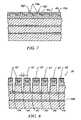
- FIG. 7is a simplified cross-sectional view after a blanket etch of the multi-layered structure, shown in FIG. 6 , to form a crown surface, in accordance with one embodiment of the present invention
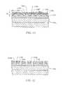
- FIG. 8is a simplified cross-sectional view of the multi-layered structure, shown in FIG. 7 , after subjecting the crown surface to an etch to form via portions in the substrate, in accordance with one embodiment of the present invention
- FIG. 9is a simplified cross-sectional view of the multi-layered structure, shown in FIG. 8 , after subjecting the crown surface to an anisotropic etch to form trench portions aligned with the via portions, in accordance with one embodiment of the present invention
- FIG. 10is a simplified cross-sectional view of the multi-layered structure, shown in FIG. 9 , after deposition of conductive material in the via portion and trench portion, in accordance with one embodiment of the present invention
- FIG. 11is a simplified cross-sectional view after a blanket etch of the multi-layered structure, shown in FIG. 6 , to form a crown surface, in accordance with a first alternate embodiment of the present invention
- FIG. 12is a simplified cross-sectional view of the multi-layered structure, shown in FIG. 11 , after subjecting the crown surface to an anisotropic etch to form a first segment of a via portion in a substrate;
- FIG. 13is a simplified cross-sectional view of the multi-layered structure, shown in FIG. 12 , after subjecting the crown surface to a blanket etch to expose regions of the patterned imprinting layer and form a second segment of a via portion;
- FIG. 14is a simplified cross-sectional view of the multi-layered structure, shown in FIG. 13 , subjecting the same to an anisotropic fluorine etch to form a trench portion and a third segment of a via portion;
- FIG. 15is a top down view of protrusions, shown in FIG. 5 , in accordance with a second alternate embodiment of the present invention.
- FIG. 16is a top down view of protrusions, shown in FIG. 5 , in accordance with a third alternate embodiment of the present invention.
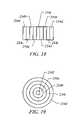
- FIG. 17is a cross-sectional view of the protrusions shown in FIG. 5 , in accordance with a fourth alternate embodiment of the present invention.
- FIG. 18is a top down view of protrusions, shown in FIG. 17 , in accordance with a fifth alternate embodiment of the present invention.
- FIG. 19is a top down view of protrusions, shown in FIG. 17 , in accordance with a sixth alternate embodiment of the present invention.
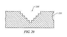
- FIG. 20is a view of a substrate having formed therein a recess that is an inverse shape of the protrusion shown in FIG. 17 ;
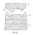
- FIG. 21is a cross-sectional view of a substrate having islands formed thereon, in accordance with a seventh alternate embodiment of the present invention.
- FIG. 22is a simplified cross-sectional view showing a mold and patterned layer having a shape complementary to the mold employed to form the protrusions shown in FIG. 21 ;
- FIG. 23is a cross-sectional view showing a crown surface formed after etching of an etch selectivity layer deposited on the patterned layer shown in FIG. 22 ;
- FIG. 24is cross-sectional view of the multi-layered structure, shown in FIG. 23 , after subjecting the crown surface to an etch to expose regions of the substrate;
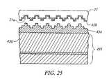
- FIG. 25is a simplified cross-sectional view of the substrate and imprint device, shown in FIG. 5 , in accordance with an eighth alternate embodiment of the present invention.
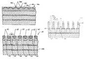
- FIG. 1depicts a lithographic system 10 in accordance with one embodiment of the present invention that includes a pair of spaced-apart bridge supports 12 having a bridge 14 and a stage support 16 extending therebetween. Bridge 14 and stage support 16 are spaced-apart. Coupled to bridge 14 is an imprint head 18 , which extends from bridge 14 toward stage support 16 . Disposed upon stage support 16 to face imprint head 18 is a motion stage 20 . Motion stage 20 is configured to move with respect to stage support 16 along X and Y axes. A radiation source 22 is coupled to system 10 to impinge actinic radiation upon motion stage 20 . As shown, radiation source 22 is coupled to bridge 14 and includes a power generator 23 connected to radiation source 22 .
- Patterned mold 27includes a surface 27 a having a pattern formed therein.
- the patternis defined by a plurality of spaced-apart recesses 28 and protuberances 29 .
- Recesses 28have a stepped shape with a groove portion 29 a flanked by stepped-portions 29 b .
- the combined width, “W C ”, of each recess 28is a sum of a width “W 1 ” of groove portion 29 a and 2W 2 , where W 2 is a width of one of stepped-portions 29 b .
- Protuberances 29have a width, “W 3 ”.
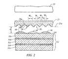
- Substrate 31typically comprises of a wafer 31 a made from a suitable material, such as silicon.
- Substrate 31may also comprise of wafer 31 a having one or more layers of material disposed thereon.
- substrate 31is shown as including multiple layers 31 c and 31 e of dielectric material, such as organosilicate glass (OSG), which has a composition of Si W C X O Y H Z .
- OSGorganosilicate glass
- Adjacent layers 31 c and 3 le of OSGmay be separated by an etch barrier 31 d made from any suitable material, such as titanium nitride (TiN).
- An additional etch barrier layer 31 bmay be positioned between dielectric layer 31 c and wafer 31 a.
- a flowable regionsuch as a patterned imprinting layer 34 , is disposed on a portion of surface 32 that presents a substantially smooth profile.
- Flowable regionmay be formed using any known technique, such as a hot embossing process disclosed in U.S. Pat. No. 5,772,905, which is incorporated by reference in its entirety herein, or a laser assisted direct imprinting (LADI) process of the type described by Chou et al. in Ultrafast and Direct Imprint of Nanostructures in Silicon , Nature, Col. 417, pp. 835-837, June 2002.
- LADIlaser assisted direct imprinting
- flowable regionconsists of patterned imprinting layer 34 being deposited as a plurality of spaced-apart discrete beads 36 of material 36 a on substrate 31 , discussed more fully below.
- Patterned imprinting layer 34is formed from a substantially silicon-free material 36 a that may be selectively polymerized and cross-linked to record the original pattern therein, defining a recorded pattern.
- Material 36 ais shown in FIG. 4 as being cross-linked at points 36 b , forming cross-linked polymer material 36 c .
- An exemplary embodiment of material 36 ais formed from a compound of approximately 48% by weight of a cyclohexyl acrylate, a monomer available from Polyscience Company, Niles Ill.; approximately 48% by weight ethylene glycol diacrylate, a cross-linking agent available from Sigma-Aldrich Corporation of St. Louis, Mo.; and approximately 4% by weight of a free radical generator sold under the tradename Darocur® and available from Ciba of Tarrytown, N.Y.
- the pattern recorded in patterned imprinting layer 34is produced, in part, by mechanical contact with patterned mold 27 .
- imprint head 18shown in FIG. 1 , is adapted to move along the Z axis and vary a distance “d” between patterned mold 27 and substrate 31 .
- patterned mold 27spreads beads 36 so as to form patterned imprinting layer 34 with a contiguous formation of material 36 a over surface 32 .
- motion stage 20may move substrate 26 along the Z-axis to allow mechanical contact between beads 36 and patterned mold 27 .
- distance “d”is reduced to allow sub-portions 34 c of patterned imprinting layer 34 to ingress into and fill recesses 28 . This facilitates the original pattern on patterned mold 27 to be imprinted into a flowable region of substrate 31 .
- material 36 ais provided with the requisite properties to completely fill recesses 28 while covering surface 32 with a contiguous formation of material 36 a .
- sub-portions 34 c of patterned imprinting layer 34 in superimposition with protuberances 29remain after the desired, usually minimum distance “d”, has been reached, leaving a projection 34 a with a thickness t 1 , shoulders 34 b with a thickness t 2 and sub-portions 34 c with a thickness t 3 .
- Projection 34 a and shoulders 34 bdefine a bi-level protrusion on surface 32 of substrate 31 .
- Sub-portion 34 cis referred to as a residual layer, and thickness t 3 is referred to as a residual thickness. Thicknesses “t 1 ”, “t 2 ” and “t 3 ” may be any thickness desired, dependent upon the application.
- radiation source 22produces actinic radiation that polymerizes and cross-links material 36 a , forming cross-linked polymer material 36 c .
- the composition of patterned imprinting layer 34transforms from material 36 a to material 36 c , which is a solid.
- material 36 cis solidified to provide side 34 d of patterned imprinting layer 34 with a shape conforming to a shape of a surface 27 a of patterned mold 27 , shown more clearly in FIG. 5 .
- a plurality of solidified bi-level protrusions 34 eis formed on substrate 31 .
- patterned imprinting layer 34is transformed to consist of material 36 c , shown in FIG. 4
- imprint head 18shown in FIG. 1 , is moved to increase distance “d” so that patterned mold 27 and patterned imprinting layer 34 are spaced-apart.
- An inverse shape of bi-level protrusions 34 eis transferred into substrate 31 to form a via portion (not shown) and a trench portion (not shown) therein.
- the dimensions of the via portion (not shown)are established as a function of the dimensions of projections 34 a
- the dimensions of the trench portion (not shown)are established as a function of the dimensions of shoulders 34 b .
- an etch selectivity layer 40shown in FIG. 6 , is disposed adjacent to patterned imprinting layer 34 after solidified bi-level protrusions 34 e have been formed.
- Substrate 31 , patterned imprinting layer 34 and etch selectivity layer 40define a multi-layered structure 38 .
- etch selectivity layer 40may be applied using any known process, including chemical vapor deposition (CVD), physical vapor deposition (PVD), sputtering and spin-on techniques. Spin-on deposition of etch selectivity layer 40 may be beneficial when recording patterns having numerous features per unit area, i.e., a dense featured pattern.
- etch selectivity layer 40is deposited employing imprint lithography processes, such as those discussed above with respect to depositing patterned imprinting layer 34 .
- etch selectivity layer 40may be formed from a polymerizable material similar to that described above with respect to FIGS.
- etch selectivity layer 40includes silicon, i.e., is a silicon-containing polymerizable material.
- An exemplary compound for use as etch selectivity layer 40is formed approximately 48% by weight of a silyl acrylate sold under product code SIA 0210 and available from Gelest, Inc. of Morrisville, Pa.; approximately 24% by weight of a Butyl Acrylate monomer available from Sigma-Aldrich Corporation of St. Louis, Mo.; approximately 24% by weight of a silyl dimethacrylate sold under product code SIB 1402 , from Gelest, Inc.
- Etch selectivity layer 40includes first and second opposed sides.
- First side 40 bfaces patterned imprinting layer 34 and has a profile complementary to the profile of the patterned imprinting layer 34 .
- the second sidefaces away from patterned imprinting layer 34 forming normalization surface 40 a .
- Normalization surface 40 ais provided with a substantially normalized profile, by ensuring that the distances, between an apex surface 34 f of each of projections 34 a and normalization surface 40 a , are substantially the same and that the distance between each of shoulders 34 b and normalization surface 40 a is substantially the same and the distance between a nadir surface 34 g of each of sub-portions 34 c , shown in FIG. 5 , and normalization surface 40 a is the same. Furthermore, as shown in FIG. 6 , substrate 31 is spaced-apart from etch selectively layer 40 . More specifically, regions of substrate 31 in superimposition with regions of imprinting layer 34 defined between protrusions 34 e , shown in FIG.5 , are spaced-apart from etch selectively layer 40 .
- One manner in which to provide normalization surface 40 a with a normalized profileinvolves use of a mold 127 having a smooth surface, i.e., featureless surface 127 a , coming into contact with etch selectivity layer 40 . As mentioned above, this may be accomplished by moving imprint head 18 , shown in FIG. 1 , along the Z-axis, moving motion stage 20 along the Z-axis, or both. Thereafter, mold 127 is separated from etch selectivity layer 40 and actinic radiation impinges upon etch selectivity layer 40 to polymerize and, therefore, solidify the same.
- a blanket etchis employed to remove portions of etch selectivity layer 40 to provide multi-layered structure 38 with a crown surface 38 a .
- An exemplary etch processemploys a CF 4 plasma etch where a predominant portion of the etch gases consists of CF 4 .
- An exemplary etch chemistryis discussed by Johnson et al. in ADVANCES IN STEP AND FLASH IMPRINT LITHOGRAPHY, in a white paper distributed at the SPIE Microlithography conference held in Santa Clara, Calif. from Feb. 23-Feb. 28, 2003.
- Crown surface 38 ais defined by an exposed apex surface 30 f of each of projections 34 a and upper surfaces of portions 40 c that remain on etch selectivity layer 40 after the blanket etch.
- crown surface 38 ais subjected to an anisotropic etch.
- the etch chemistry of the anisotropic etchis selected to maximize etching of projections 34 a and the segments of patterned imprinting layer 34 , shown in FIG. 6 , in superimposition therewith, while minimizing etching of the portions 40 c .
- advantagewas taken of the distinction of the silicon content between the patterned imprinting layer 34 and the etch selectivity layer 40 . Specifically, employing a plasma etch in which oxygen is the predominant gas, it was determined that an in-situ hardened mask 42 would be created in the regions of portions 40 c proximate to crown surface 38 a .
- a fluorine-based plasma etchsuch as a type employing CF 4 gases discussed by Johnson et al. in ADVANCES IN STEP AND FLASH IMPRINT LITHOGRAPHY, in a white paper distributed at the SPIE Microlithography conference held in Santa Clara, Calif. from Feb. 23-Feb. 28, 2003, is employed to remove regions of multi-layered structure 38 in superimposition with hardened mask 42 , shown in FIG. 7 , to expose regions 45 a and 45 b , shown in FIG. 9 , each of which has a width U′, which is optimally equal to W 2 .
- Regions 45 a and 45 bdefine a groove portion 46 and a throughway 48 extending from regions 45 a and 45 b to region 47 defining a via portion.
- the groove portion 46defines a trench portion
- throughway 48defines a via portion.
- a subsequent etch processis employed to remove remaining portions of layers 34 and 40 .
- the via portion and the trench portionmay be concurrently filled with a conductive material, such as aluminum, copper, tungsten, titanium, ti-tungsten or a combination thereof and the like, to form a contact 50 and a conductive line 52 , shown in FIG. 10 .
- the advantages of this processare manifold.
- the relative etch rate between portions 40 c and exposed apex surface 30 fmay be in a range of about 1.5:1 to about 100:1 due to the presence of the hardened mask 42 .
- self-aligned vias and trenchesmay be formed in substrate 31 while precisely controlling the dimensions thereof. This reduces transfer distortions of the pattern on the inverse shape of bi-level protrusions 34 e , shown in FIG. 5 , into substrate 31 .
- the control of dimensional widths U and U′becomes relatively independent of residual thickness t 3 .
- the rate at which the polymerizable fluid fills the pattern on patterned mold 27is inversely proportional to the cube of residual thickness t 3 .
- residual thickness t 3may be selected to maximize throughput without substantially increasing transfer distortions.
- forming patterned imprinting layer 34 from a substantially silicon-free polymerizable fluideases the cleaning process of patterned mold 27 , especially considering that patterned mold 27 is often formed from fused silica.
- an additional advantage with the present inventionis that the need to use etch barrier layers 31 d and 31 b may be abrogated.
- the overall dielectric constant of substrate 31may be reduced, thereby making this process suitable for fabricating vias and trenches in furtherance of the fabrication of high speed integrated circuits.
- etch conditionsare established so that the material from which etch selectivity layer, shown in regions 140 c , and dielectric layer 131 c are established to be substantially inert to the etch chemistry employed to remove material from which patterned imprinting layer 34 is formed.
- the material from which regions 140 c and dielectric layer 131 c are formedis relatively inert to an oxygen plasma etch.
- crown surface 138 aformed in a manner discussed above with respect to crown surface 38 a in FIG. 7 , is subjected to an oxygen plasma etch.
- apex surface 130 fis removed along with the entire extent of projection 134 a , shown as m 1 , along with all material superimposed thereby in imprinting material layer 134 .
- a first segment 148 a of via portionis formed.
- a subsequent blanket plasma etchis employed using a fluorine-based chemistry, as discussed above.
- the blanket etchremoves hardened mask 142 and regions 140 c , shown in FIG. 11 , to expose shoulders 134 b , shown in FIG. 13 .
- a second segment 148 b of via portion(not shown) is formed by removal of material of dielectric layer 131 c , shown as m 2 .
- an anisotropic oxygen-based plasma etchis employed to remove hardened shoulders 134 b , as well as material of imprinting material layer 134 in superimposition therewith to expose regions 145 a and 145 b of dielectric layer 131 c , thereby forming a trench portion 146 .
- a third segment 148 c of the via portionis formed by removal of material of dielectric layer 131 c , shown as m 3 .
- the combined length of via segments 148 a , 148 b and 148 cdefine a via portion 148 that is aligned with trench portion 146 . In this manner, a self-aligned via and trench may be fabricated.
- each protrusion 34 emay be a pair of spaced-apart shoulders 34 b equally spaced from apex surface 34 f a height h 1 and flanking projection 34 a .
- protrusion 134 emay include a single shoulder 134 b concentric about apex surface 134 f , shown in FIG. 16 .
- each protrusion 234 emay include a plurality of shoulders 234 a , 234 b , 234 c and 234 d , spaced-apart from apex surface 234 f at differing heights h 1 , h 2 , h 3 and h 4 , respectively.
- shoulders 234 a , 234 b , 234 c and 234 dare shown, in reality any number may be included from 0 to n, where “n” is an integer number.
- a mold(not shown) would have one or more recesses formed into a surface thereof that would be complementary to the shape of protrusion 234 e .
- shoulders 234 a , 234 b , 234 c and 234 dmay flank apex surface 234 f , as shown in FIG. 18 .
- shoulders 234 a , 234 b , 234 c and 234 dmay be concentrically disposed about apex surface 234 f , as shown in FIG. 19 .
- a substrate 231may be formed to have a recess complementary to the shape of protrusion 234 e , shown as 250 in FIG. 20 .
- substrate 231is shown as being from a homogenous material, e.g. silicon, any number of layers (not shown) of material may be included on substrate 231 and recess 250 may be formed in one or more of the aforementioned layers and/or substrate 231 .
- the layersmay consist of any material suitable for semiconductor processing.
- mold 327shown in FIG. 22 , includes one or more protrusions 328 extending from a surface 328 a having a projection 328 b and shoulder 328 c spaced-apart from projection 328 b between surface 328 a and projection 328 b .
- a layer of imprinting materialis disposed on substrate 331 and spread to form a patterned layer 334 as discussed above.
- patterned layer 334includes a pattern complementary to the pattern on mold 327 . In the present example, this results in one or more recesses 334 a being formed in patterned layer 334 .
- an etch selectivity layer 340is disposed upon patterned layer 334 and a crown surface 340 a to form a multi-layered structure 338 formed as discussed above.
- the only portions of etch selectivity layer 340 remaining after formation of crown surface 340 afills recesses 334 a .
- Crown surface 340 ais exposed to an oxygen etch chemistry that is highly selective in portions of patterned layer 334 not superimposed by recesses 334 a and is removed to expose regions 344 of substrate 331 , shown in FIG. 24 .
- Thisis achieved, in part, due to a hardened mask 342 that is formed by the silicon present in the remaining portions of etch selectivity layer 340 when exposed to a plasma etch using a chemistry that is predominantly composed of oxygen gases, as discussed above.
- a fluorine-based plasma etchsuch as a type discussed above, is employed to remove regions of multi-layered structure 338 , shown in FIG. 23 , in superimposition with hardened mask 342 to expose regions 345 .
- the etch rate differential between regions 344 and hardened mask 342results in the formation of islands 335 .
- substrate 331is shown as being from a homogenous material, e.g. silicon, any number of layers (not shown) of material may be included on substrate 331 and islands 335 may be formed in one or more of the aforementioned layers and/or substrate 331 .
- the layersmay consist of any material suitable for semiconductor processing.
- an exemplary radiation source 22may produce ultraviolet radiation.
- Other radiation sourcesmay be employed, such as thermal, electromagnetic and the like.
- the selection of radiation employed to initiate the polymerization of the material in patterned imprinting layer 34is known to one skilled in the art and typically depends on the specific application which is desired.
- Radiation source 22is located so that patterned mold 27 is positioned between radiation source 22 and substrate 31 .
- substrate 31 and/or patterned mold 27may be fabricated from materials that allow the same to be substantially transparent to the radiation produced by radiation source 22 .
- Exemplary materialsinclude, but are not limited to, fused-silica, quartz, silicon, organic polymers, siloxane polymers, borosilicate glass, fluorocarbon polymers, metal, and combinations of the above.
- bridge supports 12 , bridge 14 , and/or stage support 16may be fabricated from one or more of the following materials: silicon carbide, iron alloys available under the trade-name INVAR®, or trade-name SUPER INVARTM, ceramics, including but not limited to ZERODUR® ceramic.
- table 24may be constructed to isolate the remaining components of system 10 from vibrations in the surrounding environment. An exemplary table 24 is available from Newport Corporation of Irvine, Calif.
- the characteristics of material 36 aare important to efficiently pattern substrate 31 in light of the unique deposition process employed.
- material 36 ais deposited on substrate 31 as a plurality of discrete and spaced-apart beads 36 .
- the combined volume of beads 36is such that the material 36 a is distributed appropriately over an area of surface 32 where patterned imprinting layer 34 is to be formed.
- patterned imprinting layer 34is spread and patterned concurrently, with the pattern being subsequently set by exposure to radiation, such as ultraviolet radiation.
- radiationsuch as ultraviolet radiation.
- material 36 ahave certain characteristics to facilitate rapid and even spreading of material 36 a in beads 36 over surface 32 so that all thicknesses t 1 are substantially uniform and all residual thicknesses t 2 are substantially uniform.
- primer layer 456functions, inter alia, to provide a standard interface with patterned imprinting layer 434 , thereby reducing the need to customize each process to the material from which substrate 431 is formed.
- primer layer 456may be formed from an organic material with the same etch characteristics as patterned imprinting layer 434 .
- Primer layer 456is fabricated in such a manner so as to possess a continuous, smooth, relatively defect-free surface that may exhibit excellent adhesion to patterned imprinting layer 434 .
- surface 27 amay be treated with a low surface energy coating 458 .
- patterned imprinting layer 434is located between primer layer 456 and coating 458 upon contact of patterned mold 27 with substrate 431 .
- Coating 458may be applied using any known process.
- processing techniquesmay include chemical vapor deposition method, physical vapor deposition, atomic layer deposition or various other techniques, brazing and the like.
- a low surface energy coatingmay be applied to mold 127 , shown in FIG. 6 .
- release properties of either patterned imprinting layer 34 or etch selectivity layer 40may be improved by including, in the material from which the same is fabricated, a compound having low surface energy, referred to as a surfactant.
- the compoundis caused to migrate to a surface of layer therewith to interface with molds 27 and/or 127 , shown in FIGS. 2 and 6 , respectively, using known techniques.
- the surfactanthas a surface energy associated therewith that is lower than a surface energy of the polymerizable material in the layer.
- the low surface energy of the surfactantprovides the desired release properties to reduce adherence of either imprinting layer 34 or etch selectivity layer 40 to molds 27 and/or 127 , shown in FIGS. 2 and 6 , respectively. It should be understood that the surfactant may be used in conjunction with, or in lieu of, low surface energy coatings 458 , shown in FIG. 25 .
Landscapes
- Engineering & Computer Science (AREA)
- Chemical & Material Sciences (AREA)
- Physics & Mathematics (AREA)
- General Physics & Mathematics (AREA)
- Nanotechnology (AREA)
- Manufacturing & Machinery (AREA)
- Chemical Kinetics & Catalysis (AREA)
- General Chemical & Material Sciences (AREA)
- Materials Engineering (AREA)
- Organic Chemistry (AREA)
- Condensed Matter Physics & Semiconductors (AREA)
- Geochemistry & Mineralogy (AREA)
- Life Sciences & Earth Sciences (AREA)
- Microelectronics & Electronic Packaging (AREA)
- Health & Medical Sciences (AREA)
- Crystallography & Structural Chemistry (AREA)
- Toxicology (AREA)
- Computer Hardware Design (AREA)
- Power Engineering (AREA)
- Mathematical Physics (AREA)
- Theoretical Computer Science (AREA)
- Mechanical Engineering (AREA)
- Metallurgy (AREA)
- Exposure Of Semiconductors, Excluding Electron Or Ion Beam Exposure (AREA)
- Shaping Of Tube Ends By Bending Or Straightening (AREA)
- Drying Of Semiconductors (AREA)
- Internal Circuitry In Semiconductor Integrated Circuit Devices (AREA)
Abstract
Description
Claims (25)
Priority Applications (8)
| Application Number | Priority Date | Filing Date | Title |
|---|---|---|---|
| US10/423,642US7396475B2 (en) | 2003-04-25 | 2003-04-25 | Method of forming stepped structures employing imprint lithography |
| JP2006513194AJP2006524919A (en) | 2003-04-25 | 2004-04-21 | Method for forming stepped structures using imprint lithography |
| EP04750426AEP1618602A2 (en) | 2003-04-25 | 2004-04-21 | A method of forming stepped structures employing imprint lithography |
| CNA2004800139131ACN1791967A (en) | 2003-04-25 | 2004-04-21 | A method of forming stepped structures employing imprint lithography |
| PCT/US2004/012313WO2004097518A2 (en) | 2003-04-25 | 2004-04-21 | A method of forming stepped structures employing imprint lithography |
| KR1020057019984AKR20060004679A (en) | 2003-04-25 | 2004-04-21 | Method of Forming Layered Structure Using Imprint Lithography |
| MYPI20041496AMY139450A (en) | 2003-04-25 | 2004-04-23 | A method of forming stepped structures employing imprint lithography |
| TW093111426ATW200502157A (en) | 2003-04-25 | 2004-04-23 | A method of forming stepped structures employing imprint lithography |
Applications Claiming Priority (1)
| Application Number | Priority Date | Filing Date | Title |
|---|---|---|---|
| US10/423,642US7396475B2 (en) | 2003-04-25 | 2003-04-25 | Method of forming stepped structures employing imprint lithography |
Publications (2)
| Publication Number | Publication Date |
|---|---|
| US20040211754A1 US20040211754A1 (en) | 2004-10-28 |
| US7396475B2true US7396475B2 (en) | 2008-07-08 |
Family
ID=33299177
Family Applications (1)
| Application Number | Title | Priority Date | Filing Date |
|---|---|---|---|
| US10/423,642Expired - LifetimeUS7396475B2 (en) | 2003-04-25 | 2003-04-25 | Method of forming stepped structures employing imprint lithography |
Country Status (8)
| Country | Link |
|---|---|
| US (1) | US7396475B2 (en) |
| EP (1) | EP1618602A2 (en) |
| JP (1) | JP2006524919A (en) |
| KR (1) | KR20060004679A (en) |
| CN (1) | CN1791967A (en) |
| MY (1) | MY139450A (en) |
| TW (1) | TW200502157A (en) |
| WO (1) | WO2004097518A2 (en) |
Cited By (91)
| Publication number | Priority date | Publication date | Assignee | Title |
|---|---|---|---|---|
| US20060125154A1 (en)* | 2004-01-15 | 2006-06-15 | Molecular Imprints, Inc. | Method to improve the flow rate of imprinting material employing an absorption layer |
| US20060137555A1 (en)* | 2004-12-23 | 2006-06-29 | Asml Netherlands B.V. | Imprint lithography |
| US20060221790A1 (en)* | 2003-07-07 | 2006-10-05 | Suh Sang W | Recording medium, method of configuring control information thereof, recording and/or reproducing method using the same, and apparatus thereof |
| US20060261518A1 (en)* | 2005-02-28 | 2006-11-23 | Board Of Regents, The University Of Texas System | Use of step and flash imprint lithography for direct imprinting of dielectric materials for dual damascene processing |
| US20070212494A1 (en)* | 2005-07-22 | 2007-09-13 | Molecular Imprints, Inc. | Method for Imprint Lithography Utilizing an Adhesion Primer Layer |
| US20080102380A1 (en)* | 2006-10-30 | 2008-05-01 | Mangat Pawitter S | High density lithographic process |
| US20080169268A1 (en)* | 2005-09-02 | 2008-07-17 | Dipietro Richard Anthony | Processes and materials for step and flash imprint lithography |
| US20080296737A1 (en)* | 2007-05-29 | 2008-12-04 | Rolf Weis | Methods for Manufacturing a Structure on or in a Substrate, Imaging Layer for Generating Sublithographic Structures, Method for Inverting a Sublithographic Pattern, Device Obtainable by Manufacturing a Structure |
| US20090026657A1 (en)* | 2007-07-20 | 2009-01-29 | Molecular Imprints, Inc. | Alignment System and Method for a Substrate in a Nano-Imprint Process |
| US20090053535A1 (en)* | 2007-08-24 | 2009-02-26 | Molecular Imprints, Inc. | Reduced Residual Formation in Etched Multi-Layer Stacks |
| US7517211B2 (en) | 2005-12-21 | 2009-04-14 | Asml Netherlands B.V. | Imprint lithography |
| US20090130598A1 (en)* | 2007-11-21 | 2009-05-21 | Molecular Imprints, Inc. | Method of Creating a Template Employing a Lift-Off Process |
| US20090133751A1 (en)* | 2007-11-28 | 2009-05-28 | Molecular Imprints, Inc. | Nanostructured Organic Solar Cells |
| US20090147237A1 (en)* | 2007-12-05 | 2009-06-11 | Molecular Imprints, Inc. | Spatial Phase Feature Location |
| US20090166682A1 (en)* | 2007-12-31 | 2009-07-02 | Scheuerlein Roy E | Methods and apparatus for forming memory lines and vias in three dimensional memory arrays using dual damascene process and imprint lithography |
| US20090166317A1 (en)* | 2007-12-26 | 2009-07-02 | Canon Kabushiki Kaisha | Method of processing substrate by imprinting |
| US7670529B2 (en) | 2005-12-08 | 2010-03-02 | Molecular Imprints, Inc. | Method and system for double-sided patterning of substrates |
| US7670530B2 (en) | 2006-01-20 | 2010-03-02 | Molecular Imprints, Inc. | Patterning substrates employing multiple chucks |
| US20100096776A1 (en)* | 2008-10-21 | 2010-04-22 | Molecular Imprints, Inc. | Reduction of Stress During Template Separation |
| US20100095862A1 (en)* | 2008-10-22 | 2010-04-22 | Molecular Imprints, Inc. | Double Sidewall Angle Nano-Imprint Template |
| US20100102469A1 (en)* | 2008-10-24 | 2010-04-29 | Molecular Imprints, Inc. | Strain and Kinetics Control During Separation Phase of Imprint Process |
| US20100110409A1 (en)* | 2008-10-30 | 2010-05-06 | Molecular Imprints, Inc. | Separation in an Imprint Lithography Process |
| US20100112220A1 (en)* | 2008-11-03 | 2010-05-06 | Molecular Imprints, Inc. | Dispense system set-up and characterization |
| US20100112236A1 (en)* | 2008-10-30 | 2010-05-06 | Molecular Imprints, Inc. | Facilitating Adhesion Between Substrate and Patterned Layer |
| US7718077B1 (en)* | 2006-07-25 | 2010-05-18 | Hewlett-Packard Development Company, L.P. | Fabricating a structure usable in an imprint lithographic process |
| US20100237042A1 (en)* | 2009-03-23 | 2010-09-23 | Intevac, Inc. | Process for optimization of island to trench ratio in patterned media |
| US20100301449A1 (en)* | 2007-12-31 | 2010-12-02 | Sandisk 3D Llc | Methods and apparatus for forming line and pillar structures for three dimensional memory arrays using a double subtractive process and imprint lithography |
| US20110031650A1 (en)* | 2009-08-04 | 2011-02-10 | Molecular Imprints, Inc. | Adjacent Field Alignment |
| US20110031651A1 (en)* | 2004-01-23 | 2011-02-10 | Molecular Imprints, Inc. | Desirable wetting and release between an imprint lithography mold and a polymerizable composition |
| US20110030770A1 (en)* | 2009-08-04 | 2011-02-10 | Molecular Imprints, Inc. | Nanostructured organic solar cells |
| US20110042352A1 (en)* | 2007-08-03 | 2011-02-24 | Canon Kabushiki Kaisha | Imprint method and processing method of substrate using the imprint method |
| US20110048518A1 (en)* | 2009-08-26 | 2011-03-03 | Molecular Imprints, Inc. | Nanostructured thin film inorganic solar cells |
| US20110049096A1 (en)* | 2009-08-26 | 2011-03-03 | Board Of Regents, The University Of Texas System | Functional Nanoparticles |
| US20110084417A1 (en)* | 2009-10-08 | 2011-04-14 | Molecular Imprints, Inc. | Large area linear array nanoimprinting |
| US20110101538A1 (en)* | 2009-11-02 | 2011-05-05 | International Business Machines Corporation | Creation of vias and trenches with different depths |
| WO2011066450A2 (en) | 2009-11-24 | 2011-06-03 | Molecular Imprints, Inc. | Adhesion layers in nanoimprint lithography |
| WO2011072202A1 (en) | 2009-12-10 | 2011-06-16 | Molecular Imprints, Inc. | Imprint lithography template |
| US20110183070A1 (en)* | 2010-01-28 | 2011-07-28 | Molecular Imprints, Inc. | Roll-to-roll imprint lithography and purging system |
| US20110183521A1 (en)* | 2010-01-27 | 2011-07-28 | Molecular Imprints, Inc. | Methods and systems of material removal and pattern transfer |
| US20110183027A1 (en)* | 2010-01-26 | 2011-07-28 | Molecular Imprints, Inc. | Micro-Conformal Templates for Nanoimprint Lithography |
| US20110180127A1 (en)* | 2010-01-28 | 2011-07-28 | Molecular Imprints, Inc. | Solar cell fabrication by nanoimprint lithography |
| US20110189329A1 (en)* | 2010-01-29 | 2011-08-04 | Molecular Imprints, Inc. | Ultra-Compliant Nanoimprint Lithography Template |
| WO2011094672A2 (en) | 2010-01-29 | 2011-08-04 | Molecular Imprints, Inc. | Nanoimprint lithography processes for forming nanoparticles |
| US20110192302A1 (en)* | 2010-02-05 | 2011-08-11 | Molecular Imprints, Inc. | Templates Having High Contrast Alignment Marks |
| WO2011100050A2 (en) | 2010-02-09 | 2011-08-18 | Molecular Imprints, Inc. | Process gas confinement for nano-imprinting |
| US20110215503A1 (en)* | 2004-11-24 | 2011-09-08 | Molecular Imprints, Inc. | Reducing Adhesion between a Conformable Region and a Mold |
| WO2011139782A1 (en) | 2010-04-27 | 2011-11-10 | Molecular Imprints, Inc. | Separation control substrate/template for nanoimprint lithography |
| US8541053B2 (en) | 2010-07-08 | 2013-09-24 | Molecular Imprints, Inc. | Enhanced densification of silicon oxide layers |
| US8557351B2 (en) | 2005-07-22 | 2013-10-15 | Molecular Imprints, Inc. | Method for adhering materials together |
| US8828297B2 (en) | 2010-11-05 | 2014-09-09 | Molecular Imprints, Inc. | Patterning of non-convex shaped nanostructures |
| WO2014145634A2 (en) | 2013-03-15 | 2014-09-18 | Canon Nanotechnologies, Inc. | Nano imprinting with reusable polymer template with metallic or oxide coating |
| US8889332B2 (en) | 2004-10-18 | 2014-11-18 | Canon Nanotechnologies, Inc. | Low-K dielectric functional imprinting materials |
| US8891080B2 (en) | 2010-07-08 | 2014-11-18 | Canon Nanotechnologies, Inc. | Contaminate detection and substrate cleaning |
| US8916200B2 (en) | 2010-11-05 | 2014-12-23 | Molecular Imprints, Inc. | Nanoimprint lithography formation of functional nanoparticles using dual release layers |
| US8926888B2 (en) | 2011-02-25 | 2015-01-06 | Board Of Regents, The University Of Texas System | Fluorinated silazane release agents in nanoimprint lithography |
| US8935981B2 (en) | 2010-09-24 | 2015-01-20 | Canon Nanotechnologies, Inc. | High contrast alignment marks through multiple stage imprinting |
| US8967992B2 (en) | 2011-04-25 | 2015-03-03 | Canon Nanotechnologies, Inc. | Optically absorptive material for alignment marks |
| US20150061189A1 (en)* | 2013-09-03 | 2015-03-05 | Sony Dadc Austria Ag | Microfluidic device |
| WO2015070054A1 (en) | 2013-11-08 | 2015-05-14 | Canon Nanotechnologies, Inc. | Low contact imprint lithography template chuck system for improved overlay correction |
| US20150155164A1 (en)* | 2012-07-16 | 2015-06-04 | Seagate Technology Llc | Patterned mask using cured spin-on-glass composition |
| WO2015089158A1 (en) | 2013-12-10 | 2015-06-18 | Canon Nanotechnologies, Inc. | Imprint lithography template and method for zero-gap imprinting |
| US9070803B2 (en) | 2010-05-11 | 2015-06-30 | Molecular Imprints, Inc. | Nanostructured solar cell |
| WO2015103232A1 (en) | 2013-12-30 | 2015-07-09 | Canon Nanotechnologies, Inc. | Methods for uniform imprint pattern transfer of sub-20 nm features |
| RU2593633C1 (en)* | 2015-05-14 | 2016-08-10 | Федеральное государственное автономное образовательное учреждение высшего образования "Дальневосточный федеральный университет" | Method of forming ordered structures on surface of semiconductor substrates |
| US9452574B2 (en) | 2011-12-19 | 2016-09-27 | Canon Nanotechnologies, Inc. | Fabrication of seamless large area master templates for imprint lithography using step and repeat tools |
| EP3141956A1 (en) | 2015-09-08 | 2017-03-15 | Canon Kabushiki Kaisha | Substrate pretreatment for reducing fill time in nanoimprint lithography |
| US9651862B2 (en) | 2013-07-12 | 2017-05-16 | Canon Nanotechnologies, Inc. | Drop pattern generation for imprint lithography with directionally-patterned templates |
| US9993962B2 (en)* | 2016-05-23 | 2018-06-12 | Canon Kabushiki Kaisha | Method of imprinting to correct for a distortion within an imprint system |
| US10035296B2 (en) | 2016-10-13 | 2018-07-31 | Canon Kabushiki Kaisha | Methods for controlling spread of imprint material |
| TWI633584B (en)* | 2016-05-25 | 2018-08-21 | 大日本印刷股份有限公司 | Die and die base, manufacturing method of imprinted die substrate, manufacturing method of imprinting die, and die |
| US10079152B1 (en) | 2017-02-24 | 2018-09-18 | Canon Kabushiki Kaisha | Method for forming planarized etch mask structures over existing topography |
| US10095106B2 (en) | 2016-03-31 | 2018-10-09 | Canon Kabushiki Kaisha | Removing substrate pretreatment compositions in nanoimprint lithography |
| US10134588B2 (en) | 2016-03-31 | 2018-11-20 | Canon Kabushiki Kaisha | Imprint resist and substrate pretreatment for reducing fill time in nanoimprint lithography |
| US10185218B2 (en) | 2014-07-25 | 2019-01-22 | Samsung Electronics Co., Ltd | Method of transferring reverse pattern by using imprint process |
| US10189188B2 (en) | 2016-05-20 | 2019-01-29 | Canon Kabushiki Kaisha | Nanoimprint lithography adhesion layer |
| US10211051B2 (en) | 2015-11-13 | 2019-02-19 | Canon Kabushiki Kaisha | Method of reverse tone patterning |
| US10274823B2 (en) | 2016-10-18 | 2019-04-30 | Molecular Imprints, Inc. | Microlithographic fabrication of structures |
| US10317793B2 (en) | 2017-03-03 | 2019-06-11 | Canon Kabushiki Kaisha | Substrate pretreatment compositions for nanoimprint lithography |
| US10488753B2 (en) | 2015-09-08 | 2019-11-26 | Canon Kabushiki Kaisha | Substrate pretreatment and etch uniformity in nanoimprint lithography |
| US10509313B2 (en) | 2016-06-28 | 2019-12-17 | Canon Kabushiki Kaisha | Imprint resist with fluorinated photoinitiator and substrate pretreatment for reducing fill time in nanoimprint lithography |
| US10578964B2 (en) | 2013-12-31 | 2020-03-03 | Canon Nanotechnologies, Inc. | Asymmetric template shape modulation for partial field imprinting |
| US20200073228A1 (en)* | 2018-08-30 | 2020-03-05 | Toshiba Memory Corporation | Original plate |
| US10606170B2 (en) | 2017-09-14 | 2020-03-31 | Canon Kabushiki Kaisha | Template for imprint lithography and methods of making and using the same |
| US10620539B2 (en) | 2016-03-31 | 2020-04-14 | Canon Kabushiki Kaisha | Curing substrate pretreatment compositions in nanoimprint lithography |
| US10627715B2 (en) | 2016-10-31 | 2020-04-21 | Canon Kabushiki Kaisha | Method for separating a nanoimprint template from a substrate |
| US10654216B2 (en) | 2016-03-30 | 2020-05-19 | Canon Kabushiki Kaisha | System and methods for nanoimprint lithography |
| US10788749B2 (en) | 2017-11-30 | 2020-09-29 | Canon Kabushiki Kaisha | System and method for improving the throughput of a nanoimprint system |
| US10838298B2 (en) | 2016-09-21 | 2020-11-17 | Molecular Imprints, Inc. | Microlithographic fabrication of structures |
| US10935883B2 (en) | 2017-09-29 | 2021-03-02 | Canon Kabushiki Kaisha | Nanoimprint template with light blocking material and method of fabrication |
| US11728210B2 (en) | 2020-03-13 | 2023-08-15 | Kioxia Corporation | Manufacturing method of original plate and semiconductor device |
| US11869866B2 (en) | 2020-03-12 | 2024-01-09 | Kioxia Corporation | Wiring formation method, method for manufacturing semiconductor device, and semiconductor device |
Families Citing this family (82)
| Publication number | Priority date | Publication date | Assignee | Title |
|---|---|---|---|---|
| US8349241B2 (en) | 2002-10-04 | 2013-01-08 | Molecular Imprints, Inc. | Method to arrange features on a substrate to replicate features having minimal dimensional variability |
| US7186656B2 (en)* | 2004-05-21 | 2007-03-06 | Molecular Imprints, Inc. | Method of forming a recessed structure employing a reverse tone process |
| US7179396B2 (en) | 2003-03-25 | 2007-02-20 | Molecular Imprints, Inc. | Positive tone bi-layer imprint lithography method |
| US7122079B2 (en) | 2004-02-27 | 2006-10-17 | Molecular Imprints, Inc. | Composition for an etching mask comprising a silicon-containing material |
| US7323417B2 (en)* | 2004-09-21 | 2008-01-29 | Molecular Imprints, Inc. | Method of forming a recessed structure employing a reverse tone process |
| US7307118B2 (en)* | 2004-11-24 | 2007-12-11 | Molecular Imprints, Inc. | Composition to reduce adhesion between a conformable region and a mold |
| US7136150B2 (en) | 2003-09-25 | 2006-11-14 | Molecular Imprints, Inc. | Imprint lithography template having opaque alignment marks |
| US7060625B2 (en)* | 2004-01-27 | 2006-06-13 | Hewlett-Packard Development Company, L.P. | Imprint stamp |
| US7906180B2 (en)* | 2004-02-27 | 2011-03-15 | Molecular Imprints, Inc. | Composition for an etching mask comprising a silicon-containing material |
| US7435074B2 (en)* | 2004-03-13 | 2008-10-14 | International Business Machines Corporation | Method for fabricating dual damascence structures using photo-imprint lithography, methods for fabricating imprint lithography molds for dual damascene structures, materials for imprintable dielectrics and equipment for photo-imprint lithography used in dual damascence patterning |
| US20050253307A1 (en)* | 2004-05-11 | 2005-11-17 | Molecualr Imprints, Inc. | Method of patterning a conductive layer on a substrate |
| US7205244B2 (en) | 2004-09-21 | 2007-04-17 | Molecular Imprints | Patterning substrates employing multi-film layers defining etch-differential interfaces |
| US7547504B2 (en) | 2004-09-21 | 2009-06-16 | Molecular Imprints, Inc. | Pattern reversal employing thick residual layers |
| US7241395B2 (en)* | 2004-09-21 | 2007-07-10 | Molecular Imprints, Inc. | Reverse tone patterning on surfaces having planarity perturbations |
| US7041604B2 (en)* | 2004-09-21 | 2006-05-09 | Molecular Imprints, Inc. | Method of patterning surfaces while providing greater control of recess anisotropy |
| US7252777B2 (en)* | 2004-09-21 | 2007-08-07 | Molecular Imprints, Inc. | Method of forming an in-situ recessed structure |
| WO2006060757A2 (en) | 2004-12-01 | 2006-06-08 | Molecular Imprints, Inc. | Eliminating printability of sub-resolution defects in imprint lithography |
| JP4641835B2 (en)* | 2005-03-16 | 2011-03-02 | リコー光学株式会社 | Method of manufacturing phase shifter optical element and element obtained |
| JP2006278622A (en)* | 2005-03-29 | 2006-10-12 | Tdk Corp | Method of forming irregular pattern and method of manufacturing information storage medium |
| JP4742665B2 (en)* | 2005-04-28 | 2011-08-10 | 旭硝子株式会社 | Method of manufacturing processed substrate processed by etching |
| JP4736522B2 (en)* | 2005-04-28 | 2011-07-27 | 旭硝子株式会社 | Method of manufacturing processed substrate processed by etching |
| US7256131B2 (en)* | 2005-07-19 | 2007-08-14 | Molecular Imprints, Inc. | Method of controlling the critical dimension of structures formed on a substrate |
| US8846195B2 (en)* | 2005-07-22 | 2014-09-30 | Canon Nanotechnologies, Inc. | Ultra-thin polymeric adhesion layer |
| US7259102B2 (en)* | 2005-09-30 | 2007-08-21 | Molecular Imprints, Inc. | Etching technique to planarize a multi-layer structure |
| US8142703B2 (en) | 2005-10-05 | 2012-03-27 | Molecular Imprints, Inc. | Imprint lithography method |
| FR2893018B1 (en)* | 2005-11-09 | 2008-03-14 | Commissariat Energie Atomique | METHOD OF FORMING MEDIA HAVING PATTERNS, SUCH AS LITHOGRAPHIC MASKS |
| GB2436163A (en)* | 2006-03-10 | 2007-09-19 | Seiko Epson Corp | Device fabrication by ink-jet printing materials into bank structures, and embossing tool |
| JP4861044B2 (en)* | 2006-04-18 | 2012-01-25 | キヤノン株式会社 | Substrate processing method and method for manufacturing member having pattern region |
| JP4810319B2 (en)* | 2006-06-09 | 2011-11-09 | キヤノン株式会社 | Processing apparatus and device manufacturing method |
| DE102006030267B4 (en)* | 2006-06-30 | 2009-04-16 | Advanced Micro Devices, Inc., Sunnyvale | Nano embossing technique with increased flexibility in terms of adjustment and shaping of structural elements |
| US20080264553A1 (en)* | 2007-04-27 | 2008-10-30 | Hewlett-Packard Development Company Lp | Embossing |
| US8142702B2 (en)* | 2007-06-18 | 2012-03-27 | Molecular Imprints, Inc. | Solvent-assisted layer formation for imprint lithography |
| US7795132B2 (en)* | 2007-07-31 | 2010-09-14 | Molecular Imprints, Inc. | Self-aligned cross-point memory fabrication |
| SG185929A1 (en)* | 2007-11-21 | 2012-12-28 | Molecular Imprints Inc | Porous template and imprinting stack for nano-imprint lithography |
| US20100072671A1 (en)* | 2008-09-25 | 2010-03-25 | Molecular Imprints, Inc. | Nano-imprint lithography template fabrication and treatment |
| US8470188B2 (en)* | 2008-10-02 | 2013-06-25 | Molecular Imprints, Inc. | Nano-imprint lithography templates |
| US20100090341A1 (en)* | 2008-10-14 | 2010-04-15 | Molecular Imprints, Inc. | Nano-patterned active layers formed by nano-imprint lithography |
| US8415010B2 (en)* | 2008-10-20 | 2013-04-09 | Molecular Imprints, Inc. | Nano-imprint lithography stack with enhanced adhesion between silicon-containing and non-silicon containing layers |
| US20100104852A1 (en)* | 2008-10-23 | 2010-04-29 | Molecular Imprints, Inc. | Fabrication of High-Throughput Nano-Imprint Lithography Templates |
| US20100109205A1 (en)* | 2008-11-04 | 2010-05-06 | Molecular Imprints, Inc. | Photocatalytic reactions in nano-imprint lithography processes |
| US20100109195A1 (en) | 2008-11-05 | 2010-05-06 | Molecular Imprints, Inc. | Release agent partition control in imprint lithography |
| US9164375B2 (en) | 2009-06-19 | 2015-10-20 | Canon Nanotechnologies, Inc. | Dual zone template chuck |
| US8913230B2 (en) | 2009-07-02 | 2014-12-16 | Canon Nanotechnologies, Inc. | Chucking system with recessed support feature |
| TWI386761B (en)* | 2009-11-06 | 2013-02-21 | Univ Nat Cheng Kung | Multi-step contact printing process |
| CN102259831A (en)* | 2010-05-27 | 2011-11-30 | 清华大学 | Three-dimensional nano structure array |
| CN102566258B (en)* | 2010-12-29 | 2013-09-18 | 中芯国际集成电路制造(上海)有限公司 | Double imprint method |
| BR102012016393A2 (en) | 2012-07-02 | 2015-04-07 | Rexam Beverage Can South America S A | Can printing device, can printing process, printed can and blanket |
| US9555616B2 (en) | 2013-06-11 | 2017-01-31 | Ball Corporation | Variable printing process using soft secondary plates and specialty inks |
| WO2014201005A1 (en) | 2013-06-11 | 2014-12-18 | Ball Corporation | Printing process using soft photopolymer plates |
| US10086602B2 (en) | 2014-11-10 | 2018-10-02 | Rexam Beverage Can South America | Method and apparatus for printing metallic beverage container bodies |
| PL3028856T3 (en) | 2014-12-04 | 2019-10-31 | Ball Beverage Packaging Europe Ltd | Printing apparatus |
| JP6632200B2 (en)* | 2015-02-27 | 2020-01-22 | キヤノン株式会社 | Pattern forming method, processing substrate manufacturing method, optical component manufacturing method, circuit board manufacturing method, electronic component manufacturing method |
| JP2016162863A (en)* | 2015-02-27 | 2016-09-05 | キヤノン株式会社 | Pattern formation method, manufacturing method for processed substrate, manufacturing method for optical component, manufacturing method for circuit board, and manufacturing method for electronic component |
| JP6437387B2 (en)* | 2015-05-25 | 2018-12-12 | 東芝メモリ株式会社 | Substrate flattening method |
| EP3347410B1 (en)* | 2015-09-08 | 2024-06-19 | Canon Kabushiki Kaisha | Substrate pretreatment and etch uniformity in nanoimprint lithography |
| JP6646888B2 (en)* | 2015-09-09 | 2020-02-14 | 大日本印刷株式会社 | Convex structure, concave structure, and method of manufacturing convex structure |
| US10131134B2 (en) | 2015-10-30 | 2018-11-20 | Canon Kabushiki Kaisha | System and method for discharging electrostatic charge in nanoimprint lithography processes |
| US10549921B2 (en) | 2016-05-19 | 2020-02-04 | Rexam Beverage Can Company | Beverage container body decorator inspection apparatus |
| TWI610804B (en)* | 2016-05-23 | 2018-01-11 | 國立成功大學 | Energy-saving Glass and Method of Manufacturing the Same |
| US11034145B2 (en) | 2016-07-20 | 2021-06-15 | Ball Corporation | System and method for monitoring and adjusting a decorator for containers |
| RU2701243C1 (en) | 2016-07-20 | 2019-09-25 | Бол Корпорейшн | System and method of adjusting paint assembly of printing machine on cylinders and tubes |
| US10739705B2 (en) | 2016-08-10 | 2020-08-11 | Ball Corporation | Method and apparatus of decorating a metallic container by digital printing to a transfer blanket |
| WO2018031814A1 (en) | 2016-08-10 | 2018-02-15 | Ball Corporation | Method and apparatus of decorating a metallic container by digital printing to a transfer blanket |
| US9761450B1 (en)* | 2016-09-26 | 2017-09-12 | International Business Machines Corporation | Forming a fin cut in a hardmask |
| US10549313B2 (en) | 2016-10-31 | 2020-02-04 | Canon Kabushiki Kaisha | Edge field imprint lithography |
| US11454883B2 (en) | 2016-11-14 | 2022-09-27 | Canon Kabushiki Kaisha | Template replication |
| US10969680B2 (en) | 2016-11-30 | 2021-04-06 | Canon Kabushiki Kaisha | System and method for adjusting a position of a template |
| JP6685886B2 (en)* | 2016-12-08 | 2020-04-22 | キオクシア株式会社 | Template and method for manufacturing semiconductor device |
| US10578984B2 (en) | 2016-12-20 | 2020-03-03 | Canon Kabushiki Kaisha | Adaptive chucking system |
| US10712660B2 (en)* | 2016-12-21 | 2020-07-14 | Canon Kabushiki Kaisha | Template for imprint lithography including a recession and an apparatus and method of using the template |
| US9971249B1 (en) | 2017-02-27 | 2018-05-15 | Canon Kabushiki Kaisha | Method and system for controlled ultraviolet light exposure |
| US10303049B2 (en) | 2017-03-22 | 2019-05-28 | Canon Kabushiki Kaisha | Reducing electric charge in imprint lithography |
| US10534259B2 (en) | 2017-03-28 | 2020-01-14 | Canon Kabushiki Kaisha | Method and system for imprint force control |
| US10866510B2 (en) | 2017-07-31 | 2020-12-15 | Canon Kabushiki Kaisha | Overlay improvement in nanoimprint lithography |
| US10996560B2 (en) | 2017-07-31 | 2021-05-04 | Canon Kabushiki Kaisha | Real-time correction of template deformation in nanoimprint lithography |
| US11036130B2 (en) | 2017-10-19 | 2021-06-15 | Canon Kabushiki Kaisha | Drop placement evaluation |
| US10409178B2 (en) | 2017-12-18 | 2019-09-10 | Canon Kabushiki Kaisha | Alignment control in nanoimprint lithography based on real-time system identification |
| US10996561B2 (en) | 2017-12-26 | 2021-05-04 | Canon Kabushiki Kaisha | Nanoimprint lithography with a six degrees-of-freedom imprint head module |
| US11815811B2 (en) | 2021-03-23 | 2023-11-14 | Canon Kabushiki Kaisha | Magnification ramp scheme to mitigate template slippage |
| US12124165B2 (en) | 2021-10-25 | 2024-10-22 | Canon Kabushiki Kaisha | Apparatus and method for optimizing actuator forces |
| JP2025068357A (en) | 2023-10-16 | 2025-04-28 | 信越化学工業株式会社 | Composition for forming resist underlayer film, resist underlayer film, method for manufacturing resist underlayer film, patterning process, and method for manufacturing semiconductor device |
| JP2025070979A (en) | 2023-10-20 | 2025-05-02 | 信越化学工業株式会社 | Composition for forming resist underlayer film, resist underlayer film, method for producing resist underlayer film, pattern forming method, and method for producing semiconductor device |
Citations (235)
| Publication number | Priority date | Publication date | Assignee | Title |
|---|---|---|---|---|
| US3783520A (en) | 1970-09-28 | 1974-01-08 | Bell Telephone Labor Inc | High accuracy alignment procedure utilizing moire patterns |
| US3810874A (en) | 1969-03-10 | 1974-05-14 | Minnesota Mining & Mfg | Polymers prepared from poly(perfluoro-alkylene oxide) compounds |
| US4070116A (en) | 1975-06-23 | 1978-01-24 | International Business Machines Corporation | Gap measuring device for defining the distance between two or more surfaces |
| DE2800476A1 (en) | 1977-01-07 | 1978-07-13 | Instruments Sa | Mass prodn. method for grids, graticules etc. - using revolving drum, belt carrying resin and UV light source for polymerisation process |
| US4119688A (en) | 1975-11-03 | 1978-10-10 | International Business Machines Corporation | Electro-lithography method |
| US4201800A (en) | 1978-04-28 | 1980-05-06 | International Business Machines Corp. | Hardened photoresist master image mask process |
| JPS5588332U (en) | 1978-12-05 | 1980-06-18 | ||
| US4267212A (en) | 1978-09-20 | 1981-05-12 | Fuji Photo Film Co., Ltd. | Spin coating process |
| JPS577931Y2 (en) | 1977-06-03 | 1982-02-16 | ||
| US4426247A (en) | 1982-04-12 | 1984-01-17 | Nippon Telegraph & Telephone Public Corporation | Method for forming micropattern |
| US4507331A (en) | 1983-12-12 | 1985-03-26 | International Business Machines Corporation | Dry process for forming positive tone micro patterns |
| US4512848A (en) | 1984-02-06 | 1985-04-23 | Exxon Research And Engineering Co. | Procedure for fabrication of microstructures over large areas using physical replication |
| US4552833A (en) | 1984-05-14 | 1985-11-12 | International Business Machines Corporation | Radiation sensitive and oxygen plasma developable resist |
| US4600309A (en) | 1982-12-30 | 1986-07-15 | Thomson-Csf | Process and apparatus for theoptical alignment of patterns in two close-up planes in an exposure means incorporating a divergent radiation source |
| US4614667A (en) | 1984-05-21 | 1986-09-30 | Minnesota Mining And Manufacturing Company | Composite low surface energy liner of perfluoropolyether |
| US4657845A (en) | 1986-01-14 | 1987-04-14 | International Business Machines Corporation | Positive tone oxygen plasma developable photoresist |
| WO1987002935A1 (en) | 1985-11-18 | 1987-05-21 | Eastman Kodak Company | Process for making optical recording media |
| US4692205A (en) | 1986-01-31 | 1987-09-08 | International Business Machines Corporation | Silicon-containing polyimides as oxygen etch stop and dual dielectric coatings |
| US4707218A (en) | 1986-10-28 | 1987-11-17 | International Business Machines Corporation | Lithographic image size reduction |
| US4731155A (en) | 1987-04-15 | 1988-03-15 | General Electric Company | Process for forming a lithographic mask |
| US4737425A (en) | 1986-06-10 | 1988-04-12 | International Business Machines Corporation | Patterned resist and process |
| JPS63138730U (en) | 1987-03-03 | 1988-09-13 | ||
| US4808511A (en) | 1987-05-19 | 1989-02-28 | International Business Machines Corporation | Vapor phase photoresist silylation process |
| US4826943A (en) | 1986-07-25 | 1989-05-02 | Oki Electric Industry Co., Ltd. | Negative resist material |
| US4848911A (en) | 1986-06-11 | 1989-07-18 | Kabushiki Kaisha Toshiba | Method for aligning first and second objects, relative to each other, and apparatus for practicing this method |
| JPH01196749A (en) | 1988-01-30 | 1989-08-08 | Hoya Corp | Manufacture of substrate for optical information recording medium |
| US4857477A (en) | 1986-09-18 | 1989-08-15 | Oki Electric Industry Co., Ltd. | Process for fabricating a semiconductor device |
| US4891303A (en) | 1988-05-26 | 1990-01-02 | Texas Instruments Incorporated | Trilayer microlithographic process using a silicon-based resist as the middle layer |
| US4908298A (en) | 1985-03-19 | 1990-03-13 | International Business Machines Corporation | Method of creating patterned multilayer films for use in production of semiconductor circuits and systems |
| US4919748A (en) | 1989-06-30 | 1990-04-24 | At&T Bell Laboratories | Method for tapered etching |
| US4921778A (en) | 1988-07-29 | 1990-05-01 | Shipley Company Inc. | Photoresist pattern fabrication employing chemically amplified metalized material |
| JPH0224848B2 (en) | 1981-11-13 | 1990-05-30 | Nippon Synthetic Chem Ind | |
| US4931351A (en) | 1987-01-12 | 1990-06-05 | Eastman Kodak Company | Bilayer lithographic process |
| JPH0292603U (en) | 1989-01-09 | 1990-07-23 | ||
| JPH02192045A (en) | 1989-01-20 | 1990-07-27 | Fujitsu Ltd | Production of optical disk substrate |
| US4959252A (en) | 1986-09-29 | 1990-09-25 | Rhone-Poulenc Chimie | Highly oriented thermotropic optical disc member |
| US4964945A (en) | 1988-12-09 | 1990-10-23 | Minnesota Mining And Manufacturing Company | Lift off patterning process on a flexible substrate |
| US4976818A (en) | 1987-10-26 | 1990-12-11 | Matsushita Electric Industrial Co., Ltd. | Fine pattern forming method |
| US4980316A (en) | 1988-07-20 | 1990-12-25 | Siemens Aktiengesellschaft | Method for producing a resist structure on a semiconductor |
| US4999280A (en) | 1989-03-17 | 1991-03-12 | International Business Machines Corporation | Spray silylation of photoresist images |
| US5028366A (en) | 1988-01-12 | 1991-07-02 | Air Products And Chemicals, Inc. | Water based mold release compositions for making molded polyurethane foam |
| US5053318A (en) | 1989-05-18 | 1991-10-01 | Shipley Company Inc. | Plasma processing with metal mask integration |
| US5071694A (en) | 1989-02-21 | 1991-12-10 | Kanegafuchi Kagaku Kogyo Kabushiki Kaisha | Multi-layer resist |
| US5074667A (en) | 1988-08-15 | 1991-12-24 | Sumitomo Heavy Industries Co. Ltd. | Position detector employing a sector fresnel zone plate |
| US5108875A (en) | 1988-07-29 | 1992-04-28 | Shipley Company Inc. | Photoresist pattern fabrication employing chemically amplified metalized material |
| US5110514A (en) | 1989-05-01 | 1992-05-05 | Soane Technologies, Inc. | Controlled casting of a shrinkable material |
| US5148036A (en) | 1989-07-18 | 1992-09-15 | Canon Kabushiki Kaisha | Multi-axis wafer position detecting system using a mark having optical power |
| US5148037A (en) | 1988-09-09 | 1992-09-15 | Canon Kabushiki Kaisha | Position detecting method and apparatus |
| US5151754A (en) | 1989-10-06 | 1992-09-29 | Kabushiki Kaisha Toshiba | Method and an apparatus for measuring a displacement between two objects and a method and an apparatus for measuring a gap distance between two objects |
| US5169494A (en) | 1989-03-27 | 1992-12-08 | Matsushita Electric Industrial Co., Ltd. | Fine pattern forming method |
| US5173393A (en) | 1989-04-24 | 1992-12-22 | Siemens Aktiengesellschaft | Etch-resistant deep ultraviolet resist process having an aromatic treating step after development |
| US5179863A (en) | 1990-03-05 | 1993-01-19 | Kabushiki Kaisha Toshiba | Method and apparatus for setting the gap distance between a mask and a wafer at a predetermined distance |
| US5198326A (en) | 1990-05-24 | 1993-03-30 | Matsushita Electric Industrial Co., Ltd. | Process for forming fine pattern |
| US5206983A (en) | 1991-06-24 | 1993-05-04 | Wisconsin Alumni Research Foundation | Method of manufacturing micromechanical devices |
| US5212147A (en) | 1991-05-15 | 1993-05-18 | Hewlett-Packard Company | Method of forming a patterned in-situ high Tc superconductive film |
| US5234793A (en) | 1989-04-24 | 1993-08-10 | Siemens Aktiengesellschaft | Method for dimensionally accurate structure transfer in bilayer technique wherein a treating step with a bulging agent is employed after development |
| US5240550A (en) | 1990-09-21 | 1993-08-31 | U.S. Philips Corp. | Method of forming at least one groove in a substrate layer |
| US5240878A (en) | 1991-04-26 | 1993-08-31 | International Business Machines Corporation | Method for forming patterned films on a substrate |
| US5242711A (en) | 1991-08-16 | 1993-09-07 | Rockwell International Corp. | Nucleation control of diamond films by microlithographic patterning |
| US5244818A (en) | 1992-04-08 | 1993-09-14 | Georgia Tech Research Corporation | Processes for lift-off of thin film materials and for the fabrication of three dimensional integrated circuits |
| US5259926A (en)* | 1991-09-24 | 1993-11-09 | Hitachi, Ltd. | Method of manufacturing a thin-film pattern on a substrate |
| US5314772A (en) | 1990-10-09 | 1994-05-24 | Arizona Board Of Regents | High resolution, multi-layer resist for microlithography and method therefor |
| US5318870A (en) | 1989-10-18 | 1994-06-07 | Massachusetts Institute Of Technology | Method of patterning a phenolic polymer film without photoactive additive through exposure to high energy radiation below 225 nm with subsequent organometallic treatment and the associated imaged article |
| US5324683A (en) | 1993-06-02 | 1994-06-28 | Motorola, Inc. | Method of forming a semiconductor structure having an air region |
| US5328810A (en) | 1990-05-07 | 1994-07-12 | Micron Technology, Inc. | Method for reducing, by a factor or 2-N, the minimum masking pitch of a photolithographic process |
| US5330881A (en) | 1989-06-02 | 1994-07-19 | Digital Equipment Corp. | Microlithographic method for producing thick, vertically-walled photoresist patterns |
| US5362606A (en) | 1989-10-18 | 1994-11-08 | Massachusetts Institute Of Technology | Positive resist pattern formation through focused ion beam exposure and surface barrier silylation |
| US5366851A (en) | 1991-07-23 | 1994-11-22 | At&T Bell Laboratories | Device fabrication process |
| US5374454A (en) | 1990-09-18 | 1994-12-20 | International Business Machines Incorporated | Method for conditioning halogenated polymeric materials and structures fabricated therewith |
| US5376810A (en) | 1992-06-26 | 1994-12-27 | California Institute Of Technology | Growth of delta-doped layers on silicon CCD/S for enhanced ultraviolet response |
| US5380474A (en) | 1993-05-20 | 1995-01-10 | Sandia Corporation | Methods for patterned deposition on a substrate |
| US5389696A (en) | 1993-09-17 | 1995-02-14 | Miles Inc. | Process for the production of molded products using internal mold release agents |
| US5417802A (en) | 1994-03-18 | 1995-05-23 | At&T Corp. | Integrated circuit manufacturing |
| US5422295A (en) | 1992-12-10 | 1995-06-06 | Samsung Electronics Co., Ltd. | Method for forming a semiconductor memory device having a vertical multi-layered storage electrode |
| US5421981A (en) | 1991-06-26 | 1995-06-06 | Ppg Industries, Inc. | Electrochemical sensor storage device |
| US5424549A (en) | 1991-12-20 | 1995-06-13 | Board Of Supervisors Of Louisiana State University And Agricultural And Mechanical College | Scanning systems for high resolution e-beam and X-ray lithography |
| US5425848A (en) | 1993-03-16 | 1995-06-20 | U.S. Philips Corporation | Method of providing a patterned relief of cured photoresist on a flat substrate surface and device for carrying out such a method |
| US5431777A (en) | 1992-09-17 | 1995-07-11 | International Business Machines Corporation | Methods and compositions for the selective etching of silicon |
| US5434107A (en) | 1994-01-28 | 1995-07-18 | Texas Instruments Incorporated | Method for planarization |
| US5439766A (en) | 1988-12-30 | 1995-08-08 | International Business Machines Corporation | Composition for photo imaging |
| US5453157A (en) | 1994-05-16 | 1995-09-26 | Texas Instruments Incorporated | Low temperature anisotropic ashing of resist for semiconductor fabrication |
| US5458520A (en) | 1994-12-13 | 1995-10-17 | International Business Machines Corporation | Method for producing planar field emission structure |
| US5468542A (en) | 1985-12-23 | 1995-11-21 | General Electric Company | Method for production of a coated substrate with controlled surface characteristics |
| US5480047A (en) | 1993-06-04 | 1996-01-02 | Sharp Kabushiki Kaisha | Method for forming a fine resist pattern |
| US5512131A (en) | 1993-10-04 | 1996-04-30 | President And Fellows Of Harvard College | Formation of microstamped patterns on surfaces and derivative articles |
| US5542978A (en) | 1994-06-10 | 1996-08-06 | Johnson & Johnson Vision Products, Inc. | Apparatus for applying a surfactant to mold surfaces |
| US5545367A (en) | 1992-04-15 | 1996-08-13 | Soane Technologies, Inc. | Rapid prototype three dimensional stereolithography |
| US5597438A (en) | 1995-09-14 | 1997-01-28 | Siemens Aktiengesellschaft | Etch chamber having three independently controlled electrodes |
| US5601641A (en) | 1992-07-21 | 1997-02-11 | Tse Industries, Inc. | Mold release composition with polybutadiene and method of coating a mold core |
| US5654238A (en) | 1995-08-03 | 1997-08-05 | International Business Machines Corporation | Method for etching vertical contact holes without substrate damage caused by directional etching |
| US5669303A (en) | 1996-03-04 | 1997-09-23 | Motorola | Apparatus and method for stamping a surface |
| US5670415A (en) | 1994-05-24 | 1997-09-23 | Depositech, Inc. | Method and apparatus for vacuum deposition of highly ionized media in an electromagnetic controlled environment |
| JPH09311460A (en)* | 1996-05-22 | 1997-12-02 | Nikon Corp | Method for manufacturing resist pattern and molding die |
| US5700626A (en) | 1994-01-12 | 1997-12-23 | Lg Semicon Co., Ltd. | Method for forming multi-layer resist pattern |
| US5725788A (en) | 1996-03-04 | 1998-03-10 | Motorola | Apparatus and method for patterning a surface |
| US5736424A (en) | 1987-02-27 | 1998-04-07 | Lucent Technologies Inc. | Device fabrication involving planarization |
| US5743998A (en) | 1995-04-19 | 1998-04-28 | Park Scientific Instruments | Process for transferring microminiature patterns using spin-on glass resist media |
| US5753014A (en) | 1993-11-12 | 1998-05-19 | Van Rijn; Cornelis Johannes Maria | Membrane filter and a method of manufacturing the same as well as a membrane |
| US5772905A (en) | 1995-11-15 | 1998-06-30 | Regents Of The University Of Minnesota | Nanoimprint lithography |
| US5776748A (en) | 1993-10-04 | 1998-07-07 | President And Fellows Of Harvard College | Method of formation of microstamped patterns on plates for adhesion of cells and other biological materials, devices and uses therefor |
| US5820769A (en) | 1995-05-24 | 1998-10-13 | Regents Of The University Of Minnesota | Method for making magnetic storage having discrete elements with quantized magnetic moments |
| US5837314A (en) | 1994-06-10 | 1998-11-17 | Johnson & Johnson Vision Products, Inc. | Method and apparatus for applying a surfactant to mold surfaces |
| US5849209A (en) | 1995-03-31 | 1998-12-15 | Johnson & Johnson Vision Products, Inc. | Mold material made with additives |
| US5849222A (en) | 1995-09-29 | 1998-12-15 | Johnson & Johnson Vision Products, Inc. | Method for reducing lens hole defects in production of contact lens blanks |
| WO1999005724A1 (en) | 1997-07-25 | 1999-02-04 | Regents Of The University Of Minnesota | Single-electron floating-gate mos memory |
| US5888650A (en) | 1996-06-03 | 1999-03-30 | Minnesota Mining And Manufacturing Company | Temperature-responsive adhesive article |
| US5895263A (en) | 1996-12-19 | 1999-04-20 | International Business Machines Corporation | Process for manufacture of integrated circuit device |
| US5900160A (en) | 1993-10-04 | 1999-05-04 | President And Fellows Of Harvard College | Methods of etching articles via microcontact printing |
| US5902491A (en)* | 1996-10-07 | 1999-05-11 | Micron Technology, Inc. | Method of removing surface protrusions from thin films |
| US5905104A (en) | 1995-12-04 | 1999-05-18 | H. B. Fuller Licensing & Financing, Inc. | Heat resistant powder coating composition |
| US5907782A (en) | 1998-08-15 | 1999-05-25 | Acer Semiconductor Manufacturing Inc. | Method of forming a multiple fin-pillar capacitor for a high density dram cell |
| US5926690A (en) | 1997-05-28 | 1999-07-20 | Advanced Micro Devices, Inc. | Run-to-run control process for controlling critical dimensions |
| US5948470A (en) | 1997-04-28 | 1999-09-07 | Harrison; Christopher | Method of nanoscale patterning and products made thereby |
| US5948570A (en) | 1995-05-26 | 1999-09-07 | Lucent Technologies Inc. | Process for dry lithographic etching |
| US5948219A (en) | 1997-05-07 | 1999-09-07 | Advanced Micro Devices, Inc. | Apparatus for selectively exposing a semiconductor topography to an electric field |
| US5962191A (en) | 1995-03-27 | 1999-10-05 | Fujitsu Limited | Resist compositions for forming resist patterns |
| US6033977A (en) | 1997-06-30 | 2000-03-07 | Siemens Aktiengesellschaft | Dual damascene structure |
| US6039897A (en) | 1996-08-28 | 2000-03-21 | University Of Washington | Multiple patterned structures on a single substrate fabricated by elastomeric micro-molding techniques |
| US6046056A (en) | 1996-06-28 | 2000-04-04 | Caliper Technologies Corporation | High throughput screening assay systems in microscale fluidic devices |
| WO2000021689A1 (en) | 1998-10-09 | 2000-04-20 | The Trustees Of Princeton University | Microscale patterning and articles formed thereby |
| US6071372A (en) | 1997-06-05 | 2000-06-06 | Applied Materials, Inc. | RF plasma etch reactor with internal inductive coil antenna and electrically conductive chamber walls |
| US6074827A (en) | 1996-07-30 | 2000-06-13 | Aclara Biosciences, Inc. | Microfluidic method for nucleic acid purification and processing |
| US6096655A (en) | 1998-09-02 | 2000-08-01 | International Business Machines, Corporation | Method for forming vias and trenches in an insulation layer for a dual-damascene multilevel interconnection structure |
| US6143412A (en) | 1997-02-10 | 2000-11-07 | President And Fellows Of Harvard College | Fabrication of carbon microstructures |
| US6150190A (en) | 1999-05-27 | 2000-11-21 | Motorola Inc. | Method of formation of buried mirror semiconductive device |
| US6150680A (en) | 1998-03-05 | 2000-11-21 | Welch Allyn, Inc. | Field effect semiconductor device having dipole barrier |
| US6150231A (en) | 1998-06-15 | 2000-11-21 | Siemens Aktiengesellschaft | Overlay measurement technique using moire patterns |
| US6168845B1 (en) | 1999-01-19 | 2001-01-02 | International Business Machines Corporation | Patterned magnetic media and method of making the same using selective oxidation |
| US6204343B1 (en) | 1996-12-11 | 2001-03-20 | 3M Innovative Properties Company | Room temperature curable resin |
| US6218316B1 (en) | 1998-10-22 | 2001-04-17 | Micron Technology, Inc. | Planarization of non-planar surfaces in device fabrication |
| US6232175B1 (en)* | 1999-10-08 | 2001-05-15 | Taiwan Semiconductor Manufacturing Co., Ltd. | Method of manufacturing double-recess crown-shaped DRAM capacitor |
| US6245581B1 (en) | 2000-04-19 | 2001-06-12 | Advanced Micro Devices, Inc. | Method and apparatus for control of critical dimension using feedback etch control |
| WO2001047003A2 (en) | 1999-12-23 | 2001-06-28 | University Of Massachusetts | Methods and apparatus for forming submicron patterns on films |
| WO2001053889A1 (en) | 2000-01-21 | 2001-07-26 | Obducat Aktiebolag | A mold for nano imprinting |
| US6274294B1 (en) | 1999-02-03 | 2001-08-14 | Electroformed Stents, Inc. | Cylindrical photolithography exposure process and apparatus |
| WO2001069317A1 (en) | 2000-03-15 | 2001-09-20 | Obducat Ab | Device for transferring a pattern to an object |
| US6309580B1 (en) | 1995-11-15 | 2001-10-30 | Regents Of The University Of Minnesota | Release surfaces, particularly for use in nanoimprint lithography |
| WO2001090816A1 (en) | 2000-05-24 | 2001-11-29 | Obducat Aktiebolag | Method in connection with the production of a template and the template thus produced |
| US6326627B1 (en) | 2000-08-02 | 2001-12-04 | Archimedes Technology Group, Inc. | Mass filtering sputtered ion source |
| US6329256B1 (en) | 1999-09-24 | 2001-12-11 | Advanced Micro Devices, Inc. | Self-aligned damascene gate formation with low gate resistance |
| US6334960B1 (en) | 1999-03-11 | 2002-01-01 | Board Of Regents, The University Of Texas System | Step and flash imprint lithography |
| WO2002007199A1 (en) | 2000-07-18 | 2002-01-24 | Nanonex Corporation | Fluid pressure imprint lithography |
| US6342097B1 (en) | 1999-04-23 | 2002-01-29 | Sdc Coatings, Inc. | Composition for providing an abrasion resistant coating on a substrate with a matched refractive index and controlled tintability |
| US6355198B1 (en) | 1996-03-15 | 2002-03-12 | President And Fellows Of Harvard College | Method of forming articles including waveguides via capillary micromolding and microtransfer molding |
| US20020042027A1 (en) | 1998-10-09 | 2002-04-11 | Chou Stephen Y. | Microscale patterning and articles formed thereby |
| US6383928B1 (en) | 1999-09-02 | 2002-05-07 | Texas Instruments Incorporated | Post copper CMP clean |
| US6387783B1 (en) | 1999-04-26 | 2002-05-14 | International Business Machines Corporation | Methods of T-gate fabrication using a hybrid resist |
| US6387787B1 (en)* | 2001-03-02 | 2002-05-14 | Motorola, Inc. | Lithographic template and method of formation and use |
| US6388253B1 (en) | 1999-06-29 | 2002-05-14 | Applied Materials, Inc. | Integrated critical dimension control for semiconductor device manufacturing |
| US6391798B1 (en) | 1987-02-27 | 2002-05-21 | Agere Systems Guardian Corp. | Process for planarization a semiconductor substrate |
| US6426288B1 (en) | 1996-08-28 | 2002-07-30 | Micron Technology, Inc. | Method for removing an upper layer of material from a semiconductor wafer |
| US6455411B1 (en) | 2000-09-11 | 2002-09-24 | Texas Instruments Incorporated | Defect and etch rate control in trench etch for dual damascene patterning of low-k dielectrics |
| US6468896B2 (en) | 1998-06-29 | 2002-10-22 | Infineon Technologies Ag | Method of fabricating semiconductor components |
| US6468853B1 (en) | 2000-08-18 | 2002-10-22 | Chartered Semiconductor Manufacturing Ltd. | Method of fabricating a shallow trench isolation structure with reduced local oxide recess near corner |
| US6468642B1 (en) | 1995-10-03 | 2002-10-22 | N.V. Bekaert S.A. | Fluorine-doped diamond-like coatings |
| US6489068B1 (en) | 2001-02-21 | 2002-12-03 | Advanced Micro Devices, Inc. | Process for observing overlay errors on lithographic masks |
| US6495430B1 (en) | 2002-05-21 | 2002-12-17 | Macronix International Co., Ltd. | Process for fabricating sharp corner-free shallow trench isolation structure |
| US6503914B1 (en) | 2000-10-23 | 2003-01-07 | Board Of Regents, The University Of Texas System | Thienopyrimidine-based inhibitors of the Src family |
| US6514672B2 (en) | 1999-06-17 | 2003-02-04 | Taiwan Semiconductor Manufacturing Company | Dry development process for a bi-layer resist system |
| US6517977B2 (en)* | 2001-03-28 | 2003-02-11 | Motorola, Inc. | Lithographic template and method of formation and use |
| US6518168B1 (en) | 1995-08-18 | 2003-02-11 | President And Fellows Of Harvard College | Self-assembled monolayer directed patterning of surfaces |
| US6518189B1 (en) | 1995-11-15 | 2003-02-11 | Regents Of The University Of Minnesota | Method and apparatus for high density nanostructures |
| US6517995B1 (en) | 1999-09-14 | 2003-02-11 | Massachusetts Institute Of Technology | Fabrication of finely featured devices by liquid embossing |
| US6534418B1 (en) | 2001-04-30 | 2003-03-18 | Advanced Micro Devices, Inc. | Use of silicon containing imaging layer to define sub-resolution gate structures |
| US6541360B1 (en) | 2001-04-30 | 2003-04-01 | Advanced Micro Devices, Inc. | Bi-layer trim etch process to form integrated circuit gate structures |
| US20030062334A1 (en) | 2001-09-25 | 2003-04-03 | Lee Hong Hie | Method for forming a micro-pattern on a substrate by using capillary force |
| US6544594B2 (en) | 1999-09-10 | 2003-04-08 | Nano-Tex, Llc | Water-repellent and soil-resistant finish for textiles |
| US20030081193A1 (en) | 2001-06-01 | 2003-05-01 | White Donald L. | Holder, system, and process for improving overlay in lithography |
| US20030080471A1 (en) | 2001-10-29 | 2003-05-01 | Chou Stephen Y. | Lithographic method for molding pattern with nanoscale features |
| US6561706B2 (en) | 2001-06-28 | 2003-05-13 | Advanced Micro Devices, Inc. | Critical dimension monitoring from latent image |
| US6565928B2 (en) | 1999-03-08 | 2003-05-20 | Tokyo Electron Limited | Film forming method and film forming apparatus |
| US6565776B1 (en) | 1999-06-11 | 2003-05-20 | Bausch & Lomb Incorporated | Lens molds with protective coatings for production of contact lenses and other ophthalmic products |
| US6566258B1 (en) | 2000-05-10 | 2003-05-20 | Applied Materials, Inc. | Bi-layer etch stop for inter-level via |
| US20030113638A1 (en) | 2001-12-18 | 2003-06-19 | Mancini David P. | Lithographic template and method of formation and use |
| US20030129542A1 (en) | 2001-10-31 | 2003-07-10 | Brewer Science, Inc. | Contact planarization materials that generate no volatile byproducts or residue during curing |
| WO2003010289A3 (en) | 2001-07-25 | 2003-07-24 | Univ Princeton | Nanochannel arrays and their preparation and use for high throughput macromolecular analysis |
| WO2003079416A1 (en) | 2002-03-15 | 2003-09-25 | Princeton University | Laser assisted direct imprint lithography |
| US6632742B2 (en) | 2001-04-18 | 2003-10-14 | Promos Technologies Inc. | Method for avoiding defects produced in the CMP process |
| US6635581B2 (en) | 2001-06-08 | 2003-10-21 | Au Optronics, Corp. | Method for forming a thin-film transistor |
| US6646662B1 (en) | 1998-05-26 | 2003-11-11 | Seiko Epson Corporation | Patterning method, patterning apparatus, patterning template, and method for manufacturing the patterning template |
| US6649272B2 (en) | 2001-11-08 | 2003-11-18 | 3M Innovative Properties Company | Coating composition comprising fluorochemical polyether silane polycondensate and use thereof |
| WO2003099536A1 (en) | 2002-05-24 | 2003-12-04 | Chou Stephen Y | Methods and apparatus of field-induced pressure imprint lithography |
| US6664306B2 (en) | 2000-09-08 | 2003-12-16 | 3M Innovative Properties Company | Crosslinkable polymeric compositions and use thereof |
| US20040008334A1 (en) | 2002-07-11 | 2004-01-15 | Sreenivasan Sidlgata V. | Step and repeat imprint lithography systems |
| US20040009673A1 (en) | 2002-07-11 | 2004-01-15 | Sreenivasan Sidlgata V. | Method and system for imprint lithography using an electric field |
| US20040007799A1 (en) | 2002-07-11 | 2004-01-15 | Choi Byung Jin | Formation of discontinuous films during an imprint lithography process |
| US6686271B2 (en) | 2000-05-15 | 2004-02-03 | Asm International N.V. | Protective layers prior to alternating layer deposition |
| US20040021254A1 (en) | 2002-08-01 | 2004-02-05 | Sreenivasan Sidlgata V. | Alignment methods for imprint lithography |
| US20040021866A1 (en) | 2002-08-01 | 2004-02-05 | Watts Michael P.C. | Scatterometry alignment for imprint lithography |
| US20040022888A1 (en) | 2002-08-01 | 2004-02-05 | Sreenivasan Sidlgata V. | Alignment systems for imprint lithography |
| US20040029041A1 (en) | 2002-02-27 | 2004-02-12 | Brewer Science, Inc. | Novel planarization method for multi-layer lithography processing |
| US6696220B2 (en) | 2000-10-12 | 2004-02-24 | Board Of Regents, The University Of Texas System | Template for room temperature, low pressure micro-and nano-imprint lithography |
| US20040036201A1 (en) | 2000-07-18 | 2004-02-26 | Princeton University | Methods and apparatus of field-induced pressure imprint lithography |
| US6703190B2 (en) | 1999-12-07 | 2004-03-09 | Infineon Technologies Ag | Method for producing resist structures |
| US20040046288A1 (en) | 2000-07-18 | 2004-03-11 | Chou Stephen Y. | Laset assisted direct imprint lithography |
| US6721529B2 (en) | 2001-09-21 | 2004-04-13 | Nexpress Solutions Llc | Release agent donor member having fluorocarbon thermoplastic random copolymer overcoat |
| US6730256B1 (en) | 2000-08-04 | 2004-05-04 | Massachusetts Institute Of Technology | Stereolithographic patterning with interlayer surface modifications |
| US6737202B2 (en) | 2002-02-22 | 2004-05-18 | Motorola, Inc. | Method of fabricating a tiered structure using a multi-layered resist stack and use |
| US6737489B2 (en) | 2001-05-21 | 2004-05-18 | 3M Innovative Properties Company | Polymers containing perfluorovinyl ethers and applications for such polymers |
| US6743713B2 (en) | 2002-05-15 | 2004-06-01 | Institute Of Microelectronics | Method of forming dual damascene pattern using dual bottom anti-reflective coatings (BARC) |
| US20040110856A1 (en) | 2002-12-04 | 2004-06-10 | Young Jung Gun | Polymer solution for nanoimprint lithography to reduce imprint temperature and pressure |
| US20040124566A1 (en) | 2002-07-11 | 2004-07-01 | Sreenivasan Sidlgata V. | Step and repeat imprint lithography processes |
| US6759325B2 (en) | 2000-05-15 | 2004-07-06 | Asm Microchemistry Oy | Sealing porous structures |
| US20040131718A1 (en) | 2000-07-18 | 2004-07-08 | Princeton University | Lithographic apparatus for fluid pressure imprint lithography |
| US20040137734A1 (en) | 1995-11-15 | 2004-07-15 | Princeton University | Compositions and processes for nanoimprinting |
| US6767983B1 (en) | 1999-03-30 | 2004-07-27 | Nippon Steel Chemical Co., Ltd. | Silicone resin and photosensitive resin composition containing the same |
| US6770852B1 (en) | 2003-02-27 | 2004-08-03 | Lam Research Corporation | Critical dimension variation compensation across a wafer by means of local wafer temperature control |
| US6774183B1 (en) | 2000-04-27 | 2004-08-10 | Bostik, Inc. | Copolyesters having improved retained adhesion |
| US20040156108A1 (en) | 2001-10-29 | 2004-08-12 | Chou Stephen Y. | Articles comprising nanoscale patterns with reduced edge roughness and methods of making same |
| US6777170B1 (en) | 2000-08-04 | 2004-08-17 | Massachusetts Institute Of Technology | Stereolithographic patterning by variable dose light delivery |
| US6776094B1 (en) | 1993-10-04 | 2004-08-17 | President & Fellows Of Harvard College | Kit For Microcontact Printing |
| US6790905B2 (en) | 2001-10-09 | 2004-09-14 | E. I. Du Pont De Nemours And Company | Highly repellent carpet protectants |
| US20040188381A1 (en)* | 2003-03-25 | 2004-09-30 | Molecular Imprints, Inc. | Positive tone bi-layer imprint lithography method |
| US20040192041A1 (en) | 2003-03-27 | 2004-09-30 | Jun-Ho Jeong | UV nanoimprint lithography process using elementwise embossed stamp and selectively additive pressurization |
| US6802870B2 (en) | 2001-05-25 | 2004-10-12 | 3M Innovative Properties Company | Method for imparting soil and stain resistance to carpet |
| US6814879B2 (en) | 2000-09-27 | 2004-11-09 | Kabushiki Kaisha Toshiba | Method for forming pattern |
| US20040224261A1 (en) | 2003-05-08 | 2004-11-11 | Resnick Douglas J. | Unitary dual damascene process using imprint lithography |
| US6820677B2 (en)* | 2002-08-20 | 2004-11-23 | Ford Motor Company | Method of making a spray formed article |
| US6830819B2 (en) | 2003-03-18 | 2004-12-14 | Xerox Corporation | Fluorosilicone release agent for fluoroelastomer fuser members |
| US20040250945A1 (en)* | 2003-06-10 | 2004-12-16 | Industrial Technology Research Institute | Method for and apparatus for bonding patterned imprint to a substrate by adhering means |
| US6849558B2 (en) | 2002-05-22 | 2005-02-01 | The Board Of Trustees Of The Leland Stanford Junior University | Replication and transfer of microstructures and nanostructures |
| US20050037143A1 (en) | 2000-07-18 | 2005-02-17 | Chou Stephen Y. | Imprint lithography with improved monitoring and control and apparatus therefor |
| WO2005031855A1 (en) | 2003-09-29 | 2005-04-07 | International Business Machines Corporation | Fabrication method |
| WO2005031299A2 (en) | 2003-05-14 | 2005-04-07 | Nantero, Inc. | Sensor platform using a non-horizontally oriented nanotube element |
| WO2004114016A3 (en) | 2003-06-09 | 2005-05-26 | Princeton University Office Of | Imprint lithography with improved monitoring and control and apparatus therefor |
| US20050253307A1 (en) | 2004-05-11 | 2005-11-17 | Molecualr Imprints, Inc. | Method of patterning a conductive layer on a substrate |
| US20060063112A1 (en) | 2004-09-21 | 2006-03-23 | Molecular Imprints, Inc. | Pattern reversal employing thick residual layers |
| US20060063387A1 (en) | 2004-09-21 | 2006-03-23 | Molecular Imprints, Inc. | Method of Patterning Surfaces While Providing Greater Control of Recess Anisotropy |
| US20060060557A1 (en)* | 2004-09-21 | 2006-03-23 | Sreenivasan Sidlgata V | Reverse tone patterning on surfaces having surface planarity perturbations |
| US20060063277A1 (en) | 2004-09-21 | 2006-03-23 | Molecular Imprints, Inc. | Method of forming an in-situ recessed structure |
| US20060138080A1 (en)* | 2002-08-01 | 2006-06-29 | Mitsuru Hasegawa | Stamper, lithographic method of using the stamper and method of forming a structure by a lithographic pattern |
| US7186656B2 (en)* | 2004-05-21 | 2007-03-06 | Molecular Imprints, Inc. | Method of forming a recessed structure employing a reverse tone process |
| US20070052461A1 (en) | 2005-08-16 | 2007-03-08 | Monolithic Power Systems, Inc. | Linear charger where the material temperature directly affects the circuit thermal control |
| US7205244B2 (en)* | 2004-09-21 | 2007-04-17 | Molecular Imprints | Patterning substrates employing multi-film layers defining etch-differential interfaces |
| US20070243279A1 (en) | 2005-01-31 | 2007-10-18 | Molecular Imprints, Inc. | Imprint Lithography Template to Facilitate Control of Liquid Movement |
Family Cites Families (3)
| Publication number | Priority date | Publication date | Assignee | Title |
|---|---|---|---|---|
| US5900881A (en)* | 1995-03-22 | 1999-05-04 | Ikedo; Tsuneo | Computer graphics circuit |
| JPH11330235A (en)* | 1998-05-11 | 1999-11-30 | Sony Corp | Method and device for working insulating layer of semiconductor device |
| KR100335070B1 (en)* | 1999-04-21 | 2002-05-03 | 백승준 | Method for forming micro pattern on substrate by using compression patterning technique |
- 2003
- 2003-04-25USUS10/423,642patent/US7396475B2/ennot_activeExpired - Lifetime
- 2004
- 2004-04-21KRKR1020057019984Apatent/KR20060004679A/ennot_activeWithdrawn
- 2004-04-21WOPCT/US2004/012313patent/WO2004097518A2/enactiveApplication Filing
- 2004-04-21CNCNA2004800139131Apatent/CN1791967A/enactivePending
- 2004-04-21JPJP2006513194Apatent/JP2006524919A/ennot_activeCeased
- 2004-04-21EPEP04750426Apatent/EP1618602A2/ennot_activeWithdrawn
- 2004-04-23MYMYPI20041496Apatent/MY139450A/enunknown
- 2004-04-23TWTW093111426Apatent/TW200502157A/enunknown
Patent Citations (263)
| Publication number | Priority date | Publication date | Assignee | Title |
|---|---|---|---|---|
| US3810874A (en) | 1969-03-10 | 1974-05-14 | Minnesota Mining & Mfg | Polymers prepared from poly(perfluoro-alkylene oxide) compounds |
| US3783520A (en) | 1970-09-28 | 1974-01-08 | Bell Telephone Labor Inc | High accuracy alignment procedure utilizing moire patterns |
| US4070116A (en) | 1975-06-23 | 1978-01-24 | International Business Machines Corporation | Gap measuring device for defining the distance between two or more surfaces |
| US4119688A (en) | 1975-11-03 | 1978-10-10 | International Business Machines Corporation | Electro-lithography method |
| DE2800476A1 (en) | 1977-01-07 | 1978-07-13 | Instruments Sa | Mass prodn. method for grids, graticules etc. - using revolving drum, belt carrying resin and UV light source for polymerisation process |
| JPS577931Y2 (en) | 1977-06-03 | 1982-02-16 | ||
| US4201800A (en) | 1978-04-28 | 1980-05-06 | International Business Machines Corp. | Hardened photoresist master image mask process |
| US4267212A (en) | 1978-09-20 | 1981-05-12 | Fuji Photo Film Co., Ltd. | Spin coating process |
| JPS5588332U (en) | 1978-12-05 | 1980-06-18 | ||
| JPH0224848B2 (en) | 1981-11-13 | 1990-05-30 | Nippon Synthetic Chem Ind | |
| US4426247A (en) | 1982-04-12 | 1984-01-17 | Nippon Telegraph & Telephone Public Corporation | Method for forming micropattern |
| US4600309A (en) | 1982-12-30 | 1986-07-15 | Thomson-Csf | Process and apparatus for theoptical alignment of patterns in two close-up planes in an exposure means incorporating a divergent radiation source |
| US4507331A (en) | 1983-12-12 | 1985-03-26 | International Business Machines Corporation | Dry process for forming positive tone micro patterns |
| US4512848A (en) | 1984-02-06 | 1985-04-23 | Exxon Research And Engineering Co. | Procedure for fabrication of microstructures over large areas using physical replication |
| US4552833A (en) | 1984-05-14 | 1985-11-12 | International Business Machines Corporation | Radiation sensitive and oxygen plasma developable resist |
| US4614667A (en) | 1984-05-21 | 1986-09-30 | Minnesota Mining And Manufacturing Company | Composite low surface energy liner of perfluoropolyether |
| US4908298A (en) | 1985-03-19 | 1990-03-13 | International Business Machines Corporation | Method of creating patterned multilayer films for use in production of semiconductor circuits and systems |
| WO1987002935A1 (en) | 1985-11-18 | 1987-05-21 | Eastman Kodak Company | Process for making optical recording media |
| US5468542A (en) | 1985-12-23 | 1995-11-21 | General Electric Company | Method for production of a coated substrate with controlled surface characteristics |
| US4657845A (en) | 1986-01-14 | 1987-04-14 | International Business Machines Corporation | Positive tone oxygen plasma developable photoresist |
| US4692205A (en) | 1986-01-31 | 1987-09-08 | International Business Machines Corporation | Silicon-containing polyimides as oxygen etch stop and dual dielectric coatings |
| US4737425A (en) | 1986-06-10 | 1988-04-12 | International Business Machines Corporation | Patterned resist and process |
| US4848911A (en) | 1986-06-11 | 1989-07-18 | Kabushiki Kaisha Toshiba | Method for aligning first and second objects, relative to each other, and apparatus for practicing this method |
| US4826943A (en) | 1986-07-25 | 1989-05-02 | Oki Electric Industry Co., Ltd. | Negative resist material |
| US4857477A (en) | 1986-09-18 | 1989-08-15 | Oki Electric Industry Co., Ltd. | Process for fabricating a semiconductor device |
| US4959252A (en) | 1986-09-29 | 1990-09-25 | Rhone-Poulenc Chimie | Highly oriented thermotropic optical disc member |
| US4707218A (en) | 1986-10-28 | 1987-11-17 | International Business Machines Corporation | Lithographic image size reduction |
| US4931351A (en) | 1987-01-12 | 1990-06-05 | Eastman Kodak Company | Bilayer lithographic process |
| US6391798B1 (en) | 1987-02-27 | 2002-05-21 | Agere Systems Guardian Corp. | Process for planarization a semiconductor substrate |
| US5736424A (en) | 1987-02-27 | 1998-04-07 | Lucent Technologies Inc. | Device fabrication involving planarization |
| JPS63138730U (en) | 1987-03-03 | 1988-09-13 | ||
| US4731155A (en) | 1987-04-15 | 1988-03-15 | General Electric Company | Process for forming a lithographic mask |
| US4808511A (en) | 1987-05-19 | 1989-02-28 | International Business Machines Corporation | Vapor phase photoresist silylation process |
| US4976818A (en) | 1987-10-26 | 1990-12-11 | Matsushita Electric Industrial Co., Ltd. | Fine pattern forming method |
| US5028366A (en) | 1988-01-12 | 1991-07-02 | Air Products And Chemicals, Inc. | Water based mold release compositions for making molded polyurethane foam |
| JPH01196749A (en) | 1988-01-30 | 1989-08-08 | Hoya Corp | Manufacture of substrate for optical information recording medium |
| US4891303A (en) | 1988-05-26 | 1990-01-02 | Texas Instruments Incorporated | Trilayer microlithographic process using a silicon-based resist as the middle layer |
| US4980316A (en) | 1988-07-20 | 1990-12-25 | Siemens Aktiengesellschaft | Method for producing a resist structure on a semiconductor |
| US5108875A (en) | 1988-07-29 | 1992-04-28 | Shipley Company Inc. | Photoresist pattern fabrication employing chemically amplified metalized material |
| US4921778A (en) | 1988-07-29 | 1990-05-01 | Shipley Company Inc. | Photoresist pattern fabrication employing chemically amplified metalized material |
| US5074667A (en) | 1988-08-15 | 1991-12-24 | Sumitomo Heavy Industries Co. Ltd. | Position detector employing a sector fresnel zone plate |
| US5148037A (en) | 1988-09-09 | 1992-09-15 | Canon Kabushiki Kaisha | Position detecting method and apparatus |
| US4964945A (en) | 1988-12-09 | 1990-10-23 | Minnesota Mining And Manufacturing Company | Lift off patterning process on a flexible substrate |
| US5439766A (en) | 1988-12-30 | 1995-08-08 | International Business Machines Corporation | Composition for photo imaging |
| JPH0292603U (en) | 1989-01-09 | 1990-07-23 | ||
| JPH02192045A (en) | 1989-01-20 | 1990-07-27 | Fujitsu Ltd | Production of optical disk substrate |
| US5071694A (en) | 1989-02-21 | 1991-12-10 | Kanegafuchi Kagaku Kogyo Kabushiki Kaisha | Multi-layer resist |
| US4999280A (en) | 1989-03-17 | 1991-03-12 | International Business Machines Corporation | Spray silylation of photoresist images |
| US5169494A (en) | 1989-03-27 | 1992-12-08 | Matsushita Electric Industrial Co., Ltd. | Fine pattern forming method |
| US5234793A (en) | 1989-04-24 | 1993-08-10 | Siemens Aktiengesellschaft | Method for dimensionally accurate structure transfer in bilayer technique wherein a treating step with a bulging agent is employed after development |
| US5173393A (en) | 1989-04-24 | 1992-12-22 | Siemens Aktiengesellschaft | Etch-resistant deep ultraviolet resist process having an aromatic treating step after development |
| US5110514A (en) | 1989-05-01 | 1992-05-05 | Soane Technologies, Inc. | Controlled casting of a shrinkable material |
| US5053318A (en) | 1989-05-18 | 1991-10-01 | Shipley Company Inc. | Plasma processing with metal mask integration |
| US5330881A (en) | 1989-06-02 | 1994-07-19 | Digital Equipment Corp. | Microlithographic method for producing thick, vertically-walled photoresist patterns |
| US4919748A (en) | 1989-06-30 | 1990-04-24 | At&T Bell Laboratories | Method for tapered etching |
| US5148036A (en) | 1989-07-18 | 1992-09-15 | Canon Kabushiki Kaisha | Multi-axis wafer position detecting system using a mark having optical power |
| US5151754A (en) | 1989-10-06 | 1992-09-29 | Kabushiki Kaisha Toshiba | Method and an apparatus for measuring a displacement between two objects and a method and an apparatus for measuring a gap distance between two objects |
| US5362606A (en) | 1989-10-18 | 1994-11-08 | Massachusetts Institute Of Technology | Positive resist pattern formation through focused ion beam exposure and surface barrier silylation |
| US5318870A (en) | 1989-10-18 | 1994-06-07 | Massachusetts Institute Of Technology | Method of patterning a phenolic polymer film without photoactive additive through exposure to high energy radiation below 225 nm with subsequent organometallic treatment and the associated imaged article |
| US5179863A (en) | 1990-03-05 | 1993-01-19 | Kabushiki Kaisha Toshiba | Method and apparatus for setting the gap distance between a mask and a wafer at a predetermined distance |
| US5328810A (en) | 1990-05-07 | 1994-07-12 | Micron Technology, Inc. | Method for reducing, by a factor or 2-N, the minimum masking pitch of a photolithographic process |
| US5527662A (en) | 1990-05-24 | 1996-06-18 | Matsushita Electric Industrial Co., Ltd. | Process for forming fine pattern |
| US5198326A (en) | 1990-05-24 | 1993-03-30 | Matsushita Electric Industrial Co., Ltd. | Process for forming fine pattern |
| US5374454A (en) | 1990-09-18 | 1994-12-20 | International Business Machines Incorporated | Method for conditioning halogenated polymeric materials and structures fabricated therewith |
| US5240550A (en) | 1990-09-21 | 1993-08-31 | U.S. Philips Corp. | Method of forming at least one groove in a substrate layer |
| US5314772A (en) | 1990-10-09 | 1994-05-24 | Arizona Board Of Regents | High resolution, multi-layer resist for microlithography and method therefor |
| US5240878A (en) | 1991-04-26 | 1993-08-31 | International Business Machines Corporation | Method for forming patterned films on a substrate |
| US5212147A (en) | 1991-05-15 | 1993-05-18 | Hewlett-Packard Company | Method of forming a patterned in-situ high Tc superconductive film |
| US5206983A (en) | 1991-06-24 | 1993-05-04 | Wisconsin Alumni Research Foundation | Method of manufacturing micromechanical devices |
| US5421981A (en) | 1991-06-26 | 1995-06-06 | Ppg Industries, Inc. | Electrochemical sensor storage device |
| US5366851A (en) | 1991-07-23 | 1994-11-22 | At&T Bell Laboratories | Device fabrication process |
| US5242711A (en) | 1991-08-16 | 1993-09-07 | Rockwell International Corp. | Nucleation control of diamond films by microlithographic patterning |
| US5259926A (en)* | 1991-09-24 | 1993-11-09 | Hitachi, Ltd. | Method of manufacturing a thin-film pattern on a substrate |
| US5424549A (en) | 1991-12-20 | 1995-06-13 | Board Of Supervisors Of Louisiana State University And Agricultural And Mechanical College | Scanning systems for high resolution e-beam and X-ray lithography |
| US5244818A (en) | 1992-04-08 | 1993-09-14 | Georgia Tech Research Corporation | Processes for lift-off of thin film materials and for the fabrication of three dimensional integrated circuits |
| US5545367A (en) | 1992-04-15 | 1996-08-13 | Soane Technologies, Inc. | Rapid prototype three dimensional stereolithography |
| US5376810A (en) | 1992-06-26 | 1994-12-27 | California Institute Of Technology | Growth of delta-doped layers on silicon CCD/S for enhanced ultraviolet response |
| US5601641A (en) | 1992-07-21 | 1997-02-11 | Tse Industries, Inc. | Mold release composition with polybutadiene and method of coating a mold core |
| US5431777A (en) | 1992-09-17 | 1995-07-11 | International Business Machines Corporation | Methods and compositions for the selective etching of silicon |
| US5422295A (en) | 1992-12-10 | 1995-06-06 | Samsung Electronics Co., Ltd. | Method for forming a semiconductor memory device having a vertical multi-layered storage electrode |
| US5425848A (en) | 1993-03-16 | 1995-06-20 | U.S. Philips Corporation | Method of providing a patterned relief of cured photoresist on a flat substrate surface and device for carrying out such a method |
| US5380474A (en) | 1993-05-20 | 1995-01-10 | Sandia Corporation | Methods for patterned deposition on a substrate |
| US5324683A (en) | 1993-06-02 | 1994-06-28 | Motorola, Inc. | Method of forming a semiconductor structure having an air region |
| US5480047A (en) | 1993-06-04 | 1996-01-02 | Sharp Kabushiki Kaisha | Method for forming a fine resist pattern |
| US5389696A (en) | 1993-09-17 | 1995-02-14 | Miles Inc. | Process for the production of molded products using internal mold release agents |
| US5776748A (en) | 1993-10-04 | 1998-07-07 | President And Fellows Of Harvard College | Method of formation of microstamped patterns on plates for adhesion of cells and other biological materials, devices and uses therefor |
| US5900160A (en) | 1993-10-04 | 1999-05-04 | President And Fellows Of Harvard College | Methods of etching articles via microcontact printing |
| US5512131A (en) | 1993-10-04 | 1996-04-30 | President And Fellows Of Harvard College | Formation of microstamped patterns on surfaces and derivative articles |
| US6776094B1 (en) | 1993-10-04 | 2004-08-17 | President & Fellows Of Harvard College | Kit For Microcontact Printing |
| US5753014A (en) | 1993-11-12 | 1998-05-19 | Van Rijn; Cornelis Johannes Maria | Membrane filter and a method of manufacturing the same as well as a membrane |
| US5700626A (en) | 1994-01-12 | 1997-12-23 | Lg Semicon Co., Ltd. | Method for forming multi-layer resist pattern |
| US5434107A (en) | 1994-01-28 | 1995-07-18 | Texas Instruments Incorporated | Method for planarization |
| US5417802A (en) | 1994-03-18 | 1995-05-23 | At&T Corp. | Integrated circuit manufacturing |
| US5453157A (en) | 1994-05-16 | 1995-09-26 | Texas Instruments Incorporated | Low temperature anisotropic ashing of resist for semiconductor fabrication |
| US5855686A (en) | 1994-05-24 | 1999-01-05 | Depositech, Inc. | Method and apparatus for vacuum deposition of highly ionized media in an electromagnetic controlled environment |
| US6035805A (en) | 1994-05-24 | 2000-03-14 | Depositech, Inc. | Method and apparatus for vacuum deposition of highly ionized media in an electromagnetic controlled environment |
| US5670415A (en) | 1994-05-24 | 1997-09-23 | Depositech, Inc. | Method and apparatus for vacuum deposition of highly ionized media in an electromagnetic controlled environment |
| US5837314A (en) | 1994-06-10 | 1998-11-17 | Johnson & Johnson Vision Products, Inc. | Method and apparatus for applying a surfactant to mold surfaces |
| US5542978A (en) | 1994-06-10 | 1996-08-06 | Johnson & Johnson Vision Products, Inc. | Apparatus for applying a surfactant to mold surfaces |
| US5458520A (en) | 1994-12-13 | 1995-10-17 | International Business Machines Corporation | Method for producing planar field emission structure |
| US5962191A (en) | 1995-03-27 | 1999-10-05 | Fujitsu Limited | Resist compositions for forming resist patterns |
| US5849209A (en) | 1995-03-31 | 1998-12-15 | Johnson & Johnson Vision Products, Inc. | Mold material made with additives |
| US5743998A (en) | 1995-04-19 | 1998-04-28 | Park Scientific Instruments | Process for transferring microminiature patterns using spin-on glass resist media |
| US5820769A (en) | 1995-05-24 | 1998-10-13 | Regents Of The University Of Minnesota | Method for making magnetic storage having discrete elements with quantized magnetic moments |
| US5956216A (en) | 1995-05-24 | 1999-09-21 | Regents Of The University Of Minnesota | Magnetic storage having discrete elements with quantized magnetic moments |
| US5948570A (en) | 1995-05-26 | 1999-09-07 | Lucent Technologies Inc. | Process for dry lithographic etching |
| US5654238A (en) | 1995-08-03 | 1997-08-05 | International Business Machines Corporation | Method for etching vertical contact holes without substrate damage caused by directional etching |
| US6518168B1 (en) | 1995-08-18 | 2003-02-11 | President And Fellows Of Harvard College | Self-assembled monolayer directed patterning of surfaces |
| US5597438A (en) | 1995-09-14 | 1997-01-28 | Siemens Aktiengesellschaft | Etch chamber having three independently controlled electrodes |
| US5849222A (en) | 1995-09-29 | 1998-12-15 | Johnson & Johnson Vision Products, Inc. | Method for reducing lens hole defects in production of contact lens blanks |
| US6468642B1 (en) | 1995-10-03 | 2002-10-22 | N.V. Bekaert S.A. | Fluorine-doped diamond-like coatings |
| US20040137734A1 (en) | 1995-11-15 | 2004-07-15 | Princeton University | Compositions and processes for nanoimprinting |
| US6828244B2 (en) | 1995-11-15 | 2004-12-07 | Regents Of The University Of Minnesota | Method and apparatus for high density nanostructures |
| US6518189B1 (en) | 1995-11-15 | 2003-02-11 | Regents Of The University Of Minnesota | Method and apparatus for high density nanostructures |
| US6809356B2 (en) | 1995-11-15 | 2004-10-26 | Regents Of The University Of Minnesota | Method and apparatus for high density nanostructures |
| US6309580B1 (en) | 1995-11-15 | 2001-10-30 | Regents Of The University Of Minnesota | Release surfaces, particularly for use in nanoimprint lithography |
| US5772905A (en) | 1995-11-15 | 1998-06-30 | Regents Of The University Of Minnesota | Nanoimprint lithography |
| US5905104A (en) | 1995-12-04 | 1999-05-18 | H. B. Fuller Licensing & Financing, Inc. | Heat resistant powder coating composition |
| US5725788A (en) | 1996-03-04 | 1998-03-10 | Motorola | Apparatus and method for patterning a surface |
| US5669303A (en) | 1996-03-04 | 1997-09-23 | Motorola | Apparatus and method for stamping a surface |
| US6355198B1 (en) | 1996-03-15 | 2002-03-12 | President And Fellows Of Harvard College | Method of forming articles including waveguides via capillary micromolding and microtransfer molding |
| JPH09311460A (en)* | 1996-05-22 | 1997-12-02 | Nikon Corp | Method for manufacturing resist pattern and molding die |
| US5888650A (en) | 1996-06-03 | 1999-03-30 | Minnesota Mining And Manufacturing Company | Temperature-responsive adhesive article |
| US6046056A (en) | 1996-06-28 | 2000-04-04 | Caliper Technologies Corporation | High throughput screening assay systems in microscale fluidic devices |
| US6074827A (en) | 1996-07-30 | 2000-06-13 | Aclara Biosciences, Inc. | Microfluidic method for nucleic acid purification and processing |
| US6039897A (en) | 1996-08-28 | 2000-03-21 | University Of Washington | Multiple patterned structures on a single substrate fabricated by elastomeric micro-molding techniques |
| US6426288B1 (en) | 1996-08-28 | 2002-07-30 | Micron Technology, Inc. | Method for removing an upper layer of material from a semiconductor wafer |
| US5902491A (en)* | 1996-10-07 | 1999-05-11 | Micron Technology, Inc. | Method of removing surface protrusions from thin films |
| US6204343B1 (en) | 1996-12-11 | 2001-03-20 | 3M Innovative Properties Company | Room temperature curable resin |
| US5895263A (en) | 1996-12-19 | 1999-04-20 | International Business Machines Corporation | Process for manufacture of integrated circuit device |
| US6143412A (en) | 1997-02-10 | 2000-11-07 | President And Fellows Of Harvard College | Fabrication of carbon microstructures |
| US5948470A (en) | 1997-04-28 | 1999-09-07 | Harrison; Christopher | Method of nanoscale patterning and products made thereby |
| US5948219A (en) | 1997-05-07 | 1999-09-07 | Advanced Micro Devices, Inc. | Apparatus for selectively exposing a semiconductor topography to an electric field |
| US5926690A (en) | 1997-05-28 | 1999-07-20 | Advanced Micro Devices, Inc. | Run-to-run control process for controlling critical dimensions |
| US6071372A (en) | 1997-06-05 | 2000-06-06 | Applied Materials, Inc. | RF plasma etch reactor with internal inductive coil antenna and electrically conductive chamber walls |
| US6033977A (en) | 1997-06-30 | 2000-03-07 | Siemens Aktiengesellschaft | Dual damascene structure |
| WO1999005724A1 (en) | 1997-07-25 | 1999-02-04 | Regents Of The University Of Minnesota | Single-electron floating-gate mos memory |
| US6150680A (en) | 1998-03-05 | 2000-11-21 | Welch Allyn, Inc. | Field effect semiconductor device having dipole barrier |
| US6646662B1 (en) | 1998-05-26 | 2003-11-11 | Seiko Epson Corporation | Patterning method, patterning apparatus, patterning template, and method for manufacturing the patterning template |
| US6150231A (en) | 1998-06-15 | 2000-11-21 | Siemens Aktiengesellschaft | Overlay measurement technique using moire patterns |
| US6468896B2 (en) | 1998-06-29 | 2002-10-22 | Infineon Technologies Ag | Method of fabricating semiconductor components |
| US20020167117A1 (en) | 1998-06-30 | 2002-11-14 | Regents Of The University Of Minnesota | Release surfaces, particularly for use in nanoimprint lithography |
| US20030034329A1 (en) | 1998-06-30 | 2003-02-20 | Chou Stephen Y. | Lithographic method for molding pattern with nanoscale depth |
| US5907782A (en) | 1998-08-15 | 1999-05-25 | Acer Semiconductor Manufacturing Inc. | Method of forming a multiple fin-pillar capacitor for a high density dram cell |
| US6096655A (en) | 1998-09-02 | 2000-08-01 | International Business Machines, Corporation | Method for forming vias and trenches in an insulation layer for a dual-damascene multilevel interconnection structure |
| US20020042027A1 (en) | 1998-10-09 | 2002-04-11 | Chou Stephen Y. | Microscale patterning and articles formed thereby |
| WO2000021689A1 (en) | 1998-10-09 | 2000-04-20 | The Trustees Of Princeton University | Microscale patterning and articles formed thereby |
| US6713238B1 (en) | 1998-10-09 | 2004-03-30 | Stephen Y. Chou | Microscale patterning and articles formed thereby |
| US20040118809A1 (en) | 1998-10-09 | 2004-06-24 | Chou Stephen Y. | Microscale patterning and articles formed thereby |
| US6218316B1 (en) | 1998-10-22 | 2001-04-17 | Micron Technology, Inc. | Planarization of non-planar surfaces in device fabrication |
| US6677252B2 (en) | 1998-10-22 | 2004-01-13 | Micron Technology, Inc. | Methods for planarization of non-planar surfaces in device fabrication |
| US6168845B1 (en) | 1999-01-19 | 2001-01-02 | International Business Machines Corporation | Patterned magnetic media and method of making the same using selective oxidation |
| US6274294B1 (en) | 1999-02-03 | 2001-08-14 | Electroformed Stents, Inc. | Cylindrical photolithography exposure process and apparatus |
| US6565928B2 (en) | 1999-03-08 | 2003-05-20 | Tokyo Electron Limited | Film forming method and film forming apparatus |
| US6334960B1 (en) | 1999-03-11 | 2002-01-01 | Board Of Regents, The University Of Texas System | Step and flash imprint lithography |
| US6719915B2 (en) | 1999-03-11 | 2004-04-13 | Board Of Regents, The University Of Texas System | Step and flash imprint lithography |
| US6767983B1 (en) | 1999-03-30 | 2004-07-27 | Nippon Steel Chemical Co., Ltd. | Silicone resin and photosensitive resin composition containing the same |
| US6342097B1 (en) | 1999-04-23 | 2002-01-29 | Sdc Coatings, Inc. | Composition for providing an abrasion resistant coating on a substrate with a matched refractive index and controlled tintability |
| US6387783B1 (en) | 1999-04-26 | 2002-05-14 | International Business Machines Corporation | Methods of T-gate fabrication using a hybrid resist |
| US6150190A (en) | 1999-05-27 | 2000-11-21 | Motorola Inc. | Method of formation of buried mirror semiconductive device |
| US6565776B1 (en) | 1999-06-11 | 2003-05-20 | Bausch & Lomb Incorporated | Lens molds with protective coatings for production of contact lenses and other ophthalmic products |
| US6514672B2 (en) | 1999-06-17 | 2003-02-04 | Taiwan Semiconductor Manufacturing Company | Dry development process for a bi-layer resist system |
| US6388253B1 (en) | 1999-06-29 | 2002-05-14 | Applied Materials, Inc. | Integrated critical dimension control for semiconductor device manufacturing |
| US6383928B1 (en) | 1999-09-02 | 2002-05-07 | Texas Instruments Incorporated | Post copper CMP clean |
| US6544594B2 (en) | 1999-09-10 | 2003-04-08 | Nano-Tex, Llc | Water-repellent and soil-resistant finish for textiles |
| US6517995B1 (en) | 1999-09-14 | 2003-02-11 | Massachusetts Institute Of Technology | Fabrication of finely featured devices by liquid embossing |
| US6329256B1 (en) | 1999-09-24 | 2001-12-11 | Advanced Micro Devices, Inc. | Self-aligned damascene gate formation with low gate resistance |
| US6232175B1 (en)* | 1999-10-08 | 2001-05-15 | Taiwan Semiconductor Manufacturing Co., Ltd. | Method of manufacturing double-recess crown-shaped DRAM capacitor |
| US6703190B2 (en) | 1999-12-07 | 2004-03-09 | Infineon Technologies Ag | Method for producing resist structures |
| WO2001047003A2 (en) | 1999-12-23 | 2001-06-28 | University Of Massachusetts | Methods and apparatus for forming submicron patterns on films |
| US6391217B2 (en) | 1999-12-23 | 2002-05-21 | University Of Massachusetts | Methods and apparatus for forming submicron patterns on films |
| WO2001053889A1 (en) | 2000-01-21 | 2001-07-26 | Obducat Aktiebolag | A mold for nano imprinting |
| WO2001069317A1 (en) | 2000-03-15 | 2001-09-20 | Obducat Ab | Device for transferring a pattern to an object |
| US6245581B1 (en) | 2000-04-19 | 2001-06-12 | Advanced Micro Devices, Inc. | Method and apparatus for control of critical dimension using feedback etch control |
| US6774183B1 (en) | 2000-04-27 | 2004-08-10 | Bostik, Inc. | Copolyesters having improved retained adhesion |
| US6566258B1 (en) | 2000-05-10 | 2003-05-20 | Applied Materials, Inc. | Bi-layer etch stop for inter-level via |
| US6759325B2 (en) | 2000-05-15 | 2004-07-06 | Asm Microchemistry Oy | Sealing porous structures |
| US6686271B2 (en) | 2000-05-15 | 2004-02-03 | Asm International N.V. | Protective layers prior to alternating layer deposition |
| WO2001090816A1 (en) | 2000-05-24 | 2001-11-29 | Obducat Aktiebolag | Method in connection with the production of a template and the template thus produced |
| US20040036201A1 (en) | 2000-07-18 | 2004-02-26 | Princeton University | Methods and apparatus of field-induced pressure imprint lithography |
| US20040131718A1 (en) | 2000-07-18 | 2004-07-08 | Princeton University | Lithographic apparatus for fluid pressure imprint lithography |
| US20020177319A1 (en) | 2000-07-18 | 2002-11-28 | Chou Stephen Y. | Fluid pressure bonding |
| US20050037143A1 (en) | 2000-07-18 | 2005-02-17 | Chou Stephen Y. | Imprint lithography with improved monitoring and control and apparatus therefor |
| US20020132482A1 (en) | 2000-07-18 | 2002-09-19 | Chou Stephen Y. | Fluid pressure imprint lithography |
| WO2002007199A1 (en) | 2000-07-18 | 2002-01-24 | Nanonex Corporation | Fluid pressure imprint lithography |
| US20040046288A1 (en) | 2000-07-18 | 2004-03-11 | Chou Stephen Y. | Laset assisted direct imprint lithography |
| US6482742B1 (en) | 2000-07-18 | 2002-11-19 | Stephen Y. Chou | Fluid pressure imprint lithography |
| US6326627B1 (en) | 2000-08-02 | 2001-12-04 | Archimedes Technology Group, Inc. | Mass filtering sputtered ion source |
| US6777170B1 (en) | 2000-08-04 | 2004-08-17 | Massachusetts Institute Of Technology | Stereolithographic patterning by variable dose light delivery |
| US6730256B1 (en) | 2000-08-04 | 2004-05-04 | Massachusetts Institute Of Technology | Stereolithographic patterning with interlayer surface modifications |
| US6468853B1 (en) | 2000-08-18 | 2002-10-22 | Chartered Semiconductor Manufacturing Ltd. | Method of fabricating a shallow trench isolation structure with reduced local oxide recess near corner |
| US6664306B2 (en) | 2000-09-08 | 2003-12-16 | 3M Innovative Properties Company | Crosslinkable polymeric compositions and use thereof |
| US6455411B1 (en) | 2000-09-11 | 2002-09-24 | Texas Instruments Incorporated | Defect and etch rate control in trench etch for dual damascene patterning of low-k dielectrics |
| US6814879B2 (en) | 2000-09-27 | 2004-11-09 | Kabushiki Kaisha Toshiba | Method for forming pattern |
| US6696220B2 (en) | 2000-10-12 | 2004-02-24 | Board Of Regents, The University Of Texas System | Template for room temperature, low pressure micro-and nano-imprint lithography |
| US6503914B1 (en) | 2000-10-23 | 2003-01-07 | Board Of Regents, The University Of Texas System | Thienopyrimidine-based inhibitors of the Src family |
| US6489068B1 (en) | 2001-02-21 | 2002-12-03 | Advanced Micro Devices, Inc. | Process for observing overlay errors on lithographic masks |
| US6387787B1 (en)* | 2001-03-02 | 2002-05-14 | Motorola, Inc. | Lithographic template and method of formation and use |
| US6580172B2 (en) | 2001-03-02 | 2003-06-17 | Motorola, Inc. | Lithographic template and method of formation and use |
| US6517977B2 (en)* | 2001-03-28 | 2003-02-11 | Motorola, Inc. | Lithographic template and method of formation and use |
| US6632742B2 (en) | 2001-04-18 | 2003-10-14 | Promos Technologies Inc. | Method for avoiding defects produced in the CMP process |
| US6541360B1 (en) | 2001-04-30 | 2003-04-01 | Advanced Micro Devices, Inc. | Bi-layer trim etch process to form integrated circuit gate structures |
| US6534418B1 (en) | 2001-04-30 | 2003-03-18 | Advanced Micro Devices, Inc. | Use of silicon containing imaging layer to define sub-resolution gate structures |
| US6737489B2 (en) | 2001-05-21 | 2004-05-18 | 3M Innovative Properties Company | Polymers containing perfluorovinyl ethers and applications for such polymers |
| US6802870B2 (en) | 2001-05-25 | 2004-10-12 | 3M Innovative Properties Company | Method for imparting soil and stain resistance to carpet |
| US20030081193A1 (en) | 2001-06-01 | 2003-05-01 | White Donald L. | Holder, system, and process for improving overlay in lithography |
| US6635581B2 (en) | 2001-06-08 | 2003-10-21 | Au Optronics, Corp. | Method for forming a thin-film transistor |
| US6561706B2 (en) | 2001-06-28 | 2003-05-13 | Advanced Micro Devices, Inc. | Critical dimension monitoring from latent image |
| US20040197843A1 (en) | 2001-07-25 | 2004-10-07 | Chou Stephen Y. | Nanochannel arrays and their preparation and use for high throughput macromolecular analysis |
| WO2003010289A3 (en) | 2001-07-25 | 2003-07-24 | Univ Princeton | Nanochannel arrays and their preparation and use for high throughput macromolecular analysis |
| US6721529B2 (en) | 2001-09-21 | 2004-04-13 | Nexpress Solutions Llc | Release agent donor member having fluorocarbon thermoplastic random copolymer overcoat |
| US20030062334A1 (en) | 2001-09-25 | 2003-04-03 | Lee Hong Hie | Method for forming a micro-pattern on a substrate by using capillary force |
| US6790905B2 (en) | 2001-10-09 | 2004-09-14 | E. I. Du Pont De Nemours And Company | Highly repellent carpet protectants |
| US20040156108A1 (en) | 2001-10-29 | 2004-08-12 | Chou Stephen Y. | Articles comprising nanoscale patterns with reduced edge roughness and methods of making same |
| US20030080472A1 (en) | 2001-10-29 | 2003-05-01 | Chou Stephen Y. | Lithographic method with bonded release layer for molding small patterns |
| US20030080471A1 (en) | 2001-10-29 | 2003-05-01 | Chou Stephen Y. | Lithographic method for molding pattern with nanoscale features |
| US20030129542A1 (en) | 2001-10-31 | 2003-07-10 | Brewer Science, Inc. | Contact planarization materials that generate no volatile byproducts or residue during curing |
| US6716767B2 (en) | 2001-10-31 | 2004-04-06 | Brewer Science, Inc. | Contact planarization materials that generate no volatile byproducts or residue during curing |
| US6649272B2 (en) | 2001-11-08 | 2003-11-18 | 3M Innovative Properties Company | Coating composition comprising fluorochemical polyether silane polycondensate and use thereof |
| US20030113638A1 (en) | 2001-12-18 | 2003-06-19 | Mancini David P. | Lithographic template and method of formation and use |
| US6737202B2 (en) | 2002-02-22 | 2004-05-18 | Motorola, Inc. | Method of fabricating a tiered structure using a multi-layered resist stack and use |
| US20040029041A1 (en) | 2002-02-27 | 2004-02-12 | Brewer Science, Inc. | Novel planarization method for multi-layer lithography processing |
| WO2003079416A1 (en) | 2002-03-15 | 2003-09-25 | Princeton University | Laser assisted direct imprint lithography |
| US6743713B2 (en) | 2002-05-15 | 2004-06-01 | Institute Of Microelectronics | Method of forming dual damascene pattern using dual bottom anti-reflective coatings (BARC) |
| US6495430B1 (en) | 2002-05-21 | 2002-12-17 | Macronix International Co., Ltd. | Process for fabricating sharp corner-free shallow trench isolation structure |
| US6849558B2 (en) | 2002-05-22 | 2005-02-01 | The Board Of Trustees Of The Leland Stanford Junior University | Replication and transfer of microstructures and nanostructures |
| WO2003099536A1 (en) | 2002-05-24 | 2003-12-04 | Chou Stephen Y | Methods and apparatus of field-induced pressure imprint lithography |
| US20040009673A1 (en) | 2002-07-11 | 2004-01-15 | Sreenivasan Sidlgata V. | Method and system for imprint lithography using an electric field |
| US20060077374A1 (en) | 2002-07-11 | 2006-04-13 | Molecular Imprints, Inc. | Step and repeat imprint lithography systems |
| US6900881B2 (en) | 2002-07-11 | 2005-05-31 | Molecular Imprints, Inc. | Step and repeat imprint lithography systems |
| US20060076717A1 (en) | 2002-07-11 | 2006-04-13 | Molecular Imprints, Inc. | Step and repeat imprint lithography processes |
| US6908861B2 (en) | 2002-07-11 | 2005-06-21 | Molecular Imprints, Inc. | Method for imprint lithography using an electric field |
| US20040008334A1 (en) | 2002-07-11 | 2004-01-15 | Sreenivasan Sidlgata V. | Step and repeat imprint lithography systems |
| US20040124566A1 (en) | 2002-07-11 | 2004-07-01 | Sreenivasan Sidlgata V. | Step and repeat imprint lithography processes |
| US20040007799A1 (en) | 2002-07-11 | 2004-01-15 | Choi Byung Jin | Formation of discontinuous films during an imprint lithography process |
| US6932934B2 (en) | 2002-07-11 | 2005-08-23 | Molecular Imprints, Inc. | Formation of discontinuous films during an imprint lithography process |
| US20040021254A1 (en) | 2002-08-01 | 2004-02-05 | Sreenivasan Sidlgata V. | Alignment methods for imprint lithography |
| US20040021866A1 (en) | 2002-08-01 | 2004-02-05 | Watts Michael P.C. | Scatterometry alignment for imprint lithography |
| US6916584B2 (en) | 2002-08-01 | 2005-07-12 | Molecular Imprints, Inc. | Alignment methods for imprint lithography |
| US20040022888A1 (en) | 2002-08-01 | 2004-02-05 | Sreenivasan Sidlgata V. | Alignment systems for imprint lithography |
| US20060138080A1 (en)* | 2002-08-01 | 2006-06-29 | Mitsuru Hasegawa | Stamper, lithographic method of using the stamper and method of forming a structure by a lithographic pattern |
| US6820677B2 (en)* | 2002-08-20 | 2004-11-23 | Ford Motor Company | Method of making a spray formed article |
| US20040110856A1 (en) | 2002-12-04 | 2004-06-10 | Young Jung Gun | Polymer solution for nanoimprint lithography to reduce imprint temperature and pressure |
| US6770852B1 (en) | 2003-02-27 | 2004-08-03 | Lam Research Corporation | Critical dimension variation compensation across a wafer by means of local wafer temperature control |
| US6830819B2 (en) | 2003-03-18 | 2004-12-14 | Xerox Corporation | Fluorosilicone release agent for fluoroelastomer fuser members |
| US7179396B2 (en)* | 2003-03-25 | 2007-02-20 | Molecular Imprints, Inc. | Positive tone bi-layer imprint lithography method |
| US20040188381A1 (en)* | 2003-03-25 | 2004-09-30 | Molecular Imprints, Inc. | Positive tone bi-layer imprint lithography method |
| US7261831B2 (en)* | 2003-03-25 | 2007-08-28 | Molecular Imprints, Inc. | Positive tone bi-layer imprint lithography method |
| US20040192041A1 (en) | 2003-03-27 | 2004-09-30 | Jun-Ho Jeong | UV nanoimprint lithography process using elementwise embossed stamp and selectively additive pressurization |
| US20040224261A1 (en) | 2003-05-08 | 2004-11-11 | Resnick Douglas J. | Unitary dual damascene process using imprint lithography |
| WO2005031299A2 (en) | 2003-05-14 | 2005-04-07 | Nantero, Inc. | Sensor platform using a non-horizontally oriented nanotube element |
| WO2004114016A3 (en) | 2003-06-09 | 2005-05-26 | Princeton University Office Of | Imprint lithography with improved monitoring and control and apparatus therefor |
| US20040250945A1 (en)* | 2003-06-10 | 2004-12-16 | Industrial Technology Research Institute | Method for and apparatus for bonding patterned imprint to a substrate by adhering means |
| WO2005031855A1 (en) | 2003-09-29 | 2005-04-07 | International Business Machines Corporation | Fabrication method |
| US20050253307A1 (en) | 2004-05-11 | 2005-11-17 | Molecualr Imprints, Inc. | Method of patterning a conductive layer on a substrate |
| US7186656B2 (en)* | 2004-05-21 | 2007-03-06 | Molecular Imprints, Inc. | Method of forming a recessed structure employing a reverse tone process |
| US20060063387A1 (en) | 2004-09-21 | 2006-03-23 | Molecular Imprints, Inc. | Method of Patterning Surfaces While Providing Greater Control of Recess Anisotropy |
| US20060060557A1 (en)* | 2004-09-21 | 2006-03-23 | Sreenivasan Sidlgata V | Reverse tone patterning on surfaces having surface planarity perturbations |
| US20060063277A1 (en) | 2004-09-21 | 2006-03-23 | Molecular Imprints, Inc. | Method of forming an in-situ recessed structure |
| US20060063112A1 (en) | 2004-09-21 | 2006-03-23 | Molecular Imprints, Inc. | Pattern reversal employing thick residual layers |
| US7205244B2 (en)* | 2004-09-21 | 2007-04-17 | Molecular Imprints | Patterning substrates employing multi-film layers defining etch-differential interfaces |
| US20070243279A1 (en) | 2005-01-31 | 2007-10-18 | Molecular Imprints, Inc. | Imprint Lithography Template to Facilitate Control of Liquid Movement |
| US20070052461A1 (en) | 2005-08-16 | 2007-03-08 | Monolithic Power Systems, Inc. | Linear charger where the material temperature directly affects the circuit thermal control |
Non-Patent Citations (83)
| Title |
|---|
| Abstract of Japanese Patent 02-24848. |
| Abstract of Japanese Patent 02-92603. |
| Abstract of Japanese Patent 55-88332. |
| Abstract of Japanese Patent 57-7931. |
| Abstract of Japanese Patent 63-138730. |
| Amato-Wierda et al., Abstract of Low Temperature Chemical Vapor Deposition of Titanium Nitride Them Films with Hydrazine and Tetrakis(dimethylamido)titanium, Electrochemical and Solid-State Ltters, vol. 2, Issue 12, pp. 613-615. Dec. 1, 1999. |
| Bailey et al., "Template for Room Temperature Low Pressure Micro- and Nano-Imprint Lithography," U.S. Appl. No. 09/976,681, filed Oct. 12, 2001. |
| Bailey et al., Step and Flash Imprint Lithography: Defect Analysis, Journal of Vacuum Science, B 19(6), pp. 2806-2810, Nov. 1, 2001. |
| Bailey et al., Step and Flash Imprint Lithography: Template Surface Treatment and Defect Analysis, Journal of Vacuum Science, B 18(6), 3572-3577, Nov. 1, 2000. |
| Bender M. et al., "Fabrication of Nanostructures using a UV-based Imprint Technique," Microelectronic Engineering, pp. 223-236, 2000. |
| Choi et al., "Design of Orientation Stages for Step and Flash Imprint Lithography," Precision Engineering, Journal of the International Societies for Precision Engineering and Nanotechnology, 2001, pp. 192-199, vol. 25. |
| Choi et al., "Flexture Based Macro Motion Translation Stage," U.S. Appl. No. 09/934,248, filed Aug. 21, 2001. |
| Choi et al., "High Precision Orientation Alignment and Gap Control Stages for Imprint Lithography Processes," U.S. Appl. No. 09/698,317, filed Oct. 27, 2000. |
| Choi et al., "Method and System of Automatic Fluid Dispensing for Imprint Lithography Processes," U.S. Appl. No. 09/908,455, filed July 17, 2001. |
| Choi et al., "Methods for High-Precision Gap and Orientation Sensing Between a Transparent Template and Substrate for Imprint Lithography," U.S. Appl. No. 09/920,341, filed Aug. 1, 2001. |
| Chou et al., "Imprint Lithography with 25-Nanometer Resolution," Science, Apr. 5, 1996, pp. 85-87, vol. 272. |
| Chou et al., "Imprint Lithography with Sub-10nm Feature Size and High Throughput," Microelectronic Engineering, 1997, pp. 237-240, vol. 35. |
| Chou et al., "Imprint of Sub-25 nm Vias and Trenches in Polymers," Applied Physics Letters, Nov. 20, 1995, pp. 3114-3116, vol. 67(21). |
| Chou et al., "Lithographically-Induced Self Assembly of Periodic Polymer Micropillar Arrays," Journal of Vacuum Science and Technology, Nov./Dec. 1999, pp. 3197-3202, vol. B 17(6). |
| Chou et al., Nanoimprint Lithography, Journal of Vacuum Science Technology B 14(16), pp. 4129-4133, Nov. 1, 1996. |
| Chou et al., Ultrafast and Direct Imprint of Nanostructures in Silicon, Nature, col. 417, (Jun. 2002), pp. 835-837, Jun. 1, 2002. |
| Chou, "Nanoimprint Lithography and Lithographically Induced Self-Assembly," MRS Bulletin, Jul. 2001, pp. 512-517. |
| Colburn et al., Characterization and Modeling of Volumetric and Mechanical Properties for Step and Flash Imprint Lithography Photopolymers, Journal of Vacuum Science Technology. vol. b. 19(6), Nov. 1, 2001. |
| Colburn et al., Development and Advantages of Step-and-Flash Lithography, Solid State Technology, Jul. 1, 2001. |
| Colburn et al., Step and Flash Imprint Lithography for sub-100 nm Patterning, Proceedings of SPIE vol. 3997, pp. 453-457, Jan. 1, 2000. |
| Colburn. et al., "Step and Flash Imprint Lithography: A New Approach to High-Resolution Patterning", Proc. of SPIE, 1999, pp. 379-389, vol. 3676. |
| Data Sheet for Cycat 4040, www.cytec.com, no date available. |
| Data Sheet for Cymel 303ULF, www.cytec.com, no date available. |
| Data Sheet for Dow Corning Z-6018, 2001, no month or day available. |
| Data Sheet for gamma-Glycidoxypropyltrimethoxysilane, www.powerchemical.net/3100.htm, Dec. 5, 2003. |
| Data Sheet for MAK (Methyl n-Amyl Ketone), www.sp-chem.com/fine<SUB>-</SUB>e, Jan. 1, 2003, no date available. |
| Data Sheet for MAK (Methyl n-Amyl Ketone), www.sp-chem.com/fine—e, Jan. 1, 2003, no date available. |
| Data Sheet for Methyl Amyl Ketone, www.arb.ca.gov/db/solvents/solvent<SUB>-</SUB>pages/Ketones-HTML/methyl<SUB>-</SUB>amyl.htm, Mar. 31, 2005. |
| Data Sheet for Methyl Amyl Ketone, www.arb.ca.gov/db/solvents/solvent—pages/Ketones-HTML/methyl—amyl.htm, Mar. 31, 2005. |
| Data Sheet for p-Toluenesulfonic Acid, NIOSH Manual of Analytical Methods (NMAM), Fourth Edition, Jan. 15, 1998. |
| Electronic Devices and Circuits, people.deas.harvard.edu/~jones/es154/lectures/lecture<SUB>-</SUB>2/materials/materials.html, Mar. 31, 2005. |
| Electronic Devices and Circuits, people.deas.harvard.edu/˜jones/es154/lectures/lecture—2/materials/materials.html, Mar. 31, 2005. |
| Feynman, Richard P., "There's Plenty of Room at the Bottom-An Invitation to Enter a New Field of Physics," 12 pp [online[ Retrieved Sep. 23, 2004 from URL: http://www.zyvex.com/nanotech/feynman.html. |
| Feynman, Richard P., "There's Plenty of Room at the Bottom-An Invitation to Enter a New Field of Physics," 12 pp. [online] Retrieved from URL: http://www.zyvex.com/nanotech/feynman.html, transcript of talk given Dec. 29, 1959. |
| Gruska et al., ICPECVD Low Temperature (less than or equal to 130 C) Deposiion of SiOx, SiOxNy and SiNx Films, 6th Israeli Conference on Plasma Science and Applications, no date. |
| Haisma et al., "Mold-Assisted Nanolithography: A Process for Reliable Pattern Replication," Journal of Vacuum Science and Technology, Nov./Dec. 1996, pp. 4124-4128, vol. B 14(6). |
| Heidari et al., "Nanoimprint Lithography at the 6 in. Wafer Scale," Journal of Vacuum Science Technology, Nov./Dec. 2000, pp. 3557-3560, vol. B, No. 18(6). |
| Hu, Shengkui et al., "Fluorescence Probe Techniques (FPT) for Measuring the Relative Efficiencies of Free-Radical Photoinitiators," S0024-9297(97)01390-9; "Macromolecules" 1998, vol. 31, pp. 4017-4113, 1998 American Chemical Society. Published on Web May 29, 1998. |
| International Chemical Safety Card for p-Toluenseulfonic Acid, www.itcilo.it/english/actrav/telearn/osh/ic/104154.htm, Dec. 5, 2003. |
| Johnson et al., "Advances in Step and Flash Imprint Lithography," SPIE Microlithography Conference, Feb. 23-28, 2003. |
| Klaus et al., SiO2 Chemical Vapor Deposition at Room Temperature Using SiCl4 and H2O with and NH3 Catalyst, J. Electrochem. Soc. 147, 2658-2664 Jan. 1, 2000. |
| Kotachi et al., "Si-Containing Positive Resist for ArF Laser Lithography," J. PhotopolymerSci. Tevhnol. 8(4) 615-622, 1995. |
| Krauss et al., "Fabrication of Nanodevices Using Sub-25nm Imprint Lithography," Appl. Phys. Lett 67(21), 3114-3116, 1995. |
| Krug et al., "Fine Patterning of Thin Sol-Gel Films," Journal of Non-Crystalline Solids, 1992, pp. 447-450, vol. 147 & 148. |
| Li et al., Exploring Low Temperature High Density Inductive Coupled Plasma Chemical Vapor Deposition (HDICPCVD) Dielectric Films for MMICs, Project Report 1002-03 for MICRO Project 02-041, no date. |
| Lin, Multi-Layer Resist Systems, Introduction to Microlithography, pp. 287-349 Feb. 14, 1983. |
| Luurtsema, Spin Coating for Rectangular Substrates, Retrieved May 23, 2002 from URL: http://buffy.eecs.berkelye.edu/IRO/Summary/97abstracts/gluurts.2.html May 23, 2002. |
| Miller et al., Fabrication of Nanometer Sized Features on Non-Flat Substrates Using a Nano-Imprint Lithography Process, SPIE Microlithography Conference Feb. 1, 2005. |
| Mirkin et al., "Emerging Methods for Micro-and Nanofabrication," MRS Bulletin, Jul. 2001, pp. 506-509. |
| Nakamatsu et al., Bilayer Resist Method for Room-Temperature Nanoimprint Lithography, Japanese Journal of Applied Physics, vol. 43, No. 6B, pp. 4050-4053 Jun. 29, 2004. |
| Nguyen, A. Q., "Asymmetric Fluid-Structure Dynamics in Nanoscale Imprint Lithography," University of Texas at Austin, Aug. 2001. |
| Nordquist et al., Image Placement Issues for ITO-based Step and Flash Imprint Lithography Templates, J. Vac. Sci. Technol. B, pp. 695-701 Mar. 1, 2004. |
| Otto et al., "Step and Repeat UV-Nanoimprint Lithography: Material Issues," Nanoimprint and Nanoprint Technology Conference, San Francisco, Dec. 11-13, 2002. |
| Otto M. et al, "Characterization and Application of a UV-based Imprint Technique," Microelectronic Engineering, pp. 361-366, 2001. |
| Photoresist Coating Methods, e-mail from Susan Bagen(BAGEN@aol.com) to Dhaval Shah Sep. 18, 1997. |
| Plasma Enhanced Chemical Vapor Deposition (PECVD), http://yuekuo.tamu.edu/pecvd.thm, no date. |
| Ruchhoeft et al., "Patterning Curved Surfaces: Template Generation by Ion Beam Proximity Lithography and Relief Transfer by Step and Flash Imprint Lithography," Journal of Vacuum Science and Technology, 1999, pp. 2965-2982, vol. 17. |
| Sahu et al., Influence of Hydrogen on Losses in Silicon Oxynitride Planar Optical Waveguides, Semicond. Sci. Technol. 15,pp. L11-L14 Mar. 1, 2000. |
| Scheer et al., "Problems of the Nanoimprinting Technique for Nanometer Scale Pattern Definition," Journal of Vacuum Science and Technology, Nov./Dec. 1998, pp. 3917-3921, vol. B 16(6). |
| Schneider et al., Stripes of Partially Fluorinated Alkyl Chains: Dipolar Langmuir Monolayers, no date available. |
| Silicon or Silica, www.mii.org/Minerals/photosil, Mar. 31, 2005. |
| Smith et al., Employing Step and Flash Imprint Lithography for Gate Level Patterning of a MOSFET Device, SPIE Microlithography Conference Feb. 1, 2003. |
| Sreenivasan et al., "High-Resolution Overlay Alignment Methods and Systems for Imprint Lithography," U.S. Appl. No. 09/907,512, filed Jul. 16, 2001. |
| Sreenivasan et al., "Step and Repeat Imprint Lithography Processes," U.S. Appl. 10/194,991, filed Jul. 11, 2002. |
| Sreenivasan et al., "Step and Repeat Imprint Lithography Systems," U.S. Appl. No. 10/194,414, filed Jul. 11, 2002. |
| Sreenivasan, "Positive Tone Bi-Layer Imprint Lithography Method," U.S. Appl. 10/396,615, filed Mar. 25, 2003. |
| Stewart et al., Direct Imprinting of Dielectric Materials for Dual Damascene Processing, SPIE Microlithography Conference Feb. 1, 2003. |
| Translation of Japanese Patent 02-24848. |
| Translation of Japanese Patent 02-92603. |
| U.S. Appl. No. 10/946,574, naming inventors Stacey et al., entitled Patterning Substrates Employing Multi-Film Layers Defining Etch-Differential Interfaces, filed Sep. 21, 2004. |
| U.S. Appl. No. 11/126,946, naming inventors Choi et al., entitled Formation of Discontinuous Films During an Imprint Lithography Process, filed May 11, 2005. |
| U.S. Appl. No. 11/184, 664, naming inventors LaBrake, entitled Method of controlling the critical dimension of structures formed on a substrate, filed Jul. 19, 2005. |
| Voisin, "Methods of Manufacturing a Lithography Template," U.S. Appl. No. 10/136,188, filed May 1, 2002. |
| Webster's II New Riverside Univ. Dictionary, 1994, p. 641.* |
| Willson et al., "Method and System for Fabricating Nanoscale Patterns in Light Curable Compositions Using an Electric Field," U.S. Appl. No. 09/905,718, filed May 16, 2002. |
| Wu et al., "Large Area High Density Quantized Magnetic Disks Fabricated Using Nanoimprint Lithography," Journal of Vacuum Science and Technology, Nov./Dec. 1998, pp. 3825-3829, vol. B 16(6). |
| Xia et al., "Soft Lithography," Agnew. Chem. Int. Ed., 1998, pp. 550-575, vol. 37. |
| Xia et al., "Soft Lithography," Annu. Rev. Mater. Sci., 1998, pp. 153-184, vol. 28. |
Cited By (158)
| Publication number | Priority date | Publication date | Assignee | Title |
|---|---|---|---|---|
| US20060221790A1 (en)* | 2003-07-07 | 2006-10-05 | Suh Sang W | Recording medium, method of configuring control information thereof, recording and/or reproducing method using the same, and apparatus thereof |
| US20060125154A1 (en)* | 2004-01-15 | 2006-06-15 | Molecular Imprints, Inc. | Method to improve the flow rate of imprinting material employing an absorption layer |
| US8268220B2 (en) | 2004-01-23 | 2012-09-18 | Molecular Imprints, Inc. | Imprint lithography method |
| US20110031651A1 (en)* | 2004-01-23 | 2011-02-10 | Molecular Imprints, Inc. | Desirable wetting and release between an imprint lithography mold and a polymerizable composition |
| US8889332B2 (en) | 2004-10-18 | 2014-11-18 | Canon Nanotechnologies, Inc. | Low-K dielectric functional imprinting materials |
| US20110215503A1 (en)* | 2004-11-24 | 2011-09-08 | Molecular Imprints, Inc. | Reducing Adhesion between a Conformable Region and a Mold |
| US8571318B2 (en) | 2004-12-23 | 2013-10-29 | Asml Netherlands B.V. | Imprint lithography |
| US20060159305A1 (en)* | 2004-12-23 | 2006-07-20 | Asml Netherlands B.V. | Imprint lithography |
| US8131078B2 (en) | 2004-12-23 | 2012-03-06 | Asml Netherlands B.V. | Imprint lithography |
| US7636475B2 (en)* | 2004-12-23 | 2009-12-22 | Asml Netherlands B.V. | Imprint lithography |
| US20100050893A1 (en)* | 2004-12-23 | 2010-03-04 | Asml Netherlands B.V. | Imprint lithography |
| US7676088B2 (en) | 2004-12-23 | 2010-03-09 | Asml Netherlands B.V. | Imprint lithography |
| US20060137555A1 (en)* | 2004-12-23 | 2006-06-29 | Asml Netherlands B.V. | Imprint lithography |
| US7691275B2 (en)* | 2005-02-28 | 2010-04-06 | Board Of Regents, The University Of Texas System | Use of step and flash imprint lithography for direct imprinting of dielectric materials for dual damascene processing |
| US20060261518A1 (en)* | 2005-02-28 | 2006-11-23 | Board Of Regents, The University Of Texas System | Use of step and flash imprint lithography for direct imprinting of dielectric materials for dual damascene processing |
| US8808808B2 (en) | 2005-07-22 | 2014-08-19 | Molecular Imprints, Inc. | Method for imprint lithography utilizing an adhesion primer layer |
| US20070212494A1 (en)* | 2005-07-22 | 2007-09-13 | Molecular Imprints, Inc. | Method for Imprint Lithography Utilizing an Adhesion Primer Layer |
| US8557351B2 (en) | 2005-07-22 | 2013-10-15 | Molecular Imprints, Inc. | Method for adhering materials together |
| US20080169268A1 (en)* | 2005-09-02 | 2008-07-17 | Dipietro Richard Anthony | Processes and materials for step and flash imprint lithography |
| US8128832B2 (en)* | 2005-09-02 | 2012-03-06 | International Business Machines Corporation | Processes and materials for step and flash imprint lithography |
| US7670529B2 (en) | 2005-12-08 | 2010-03-02 | Molecular Imprints, Inc. | Method and system for double-sided patterning of substrates |
| US20090212462A1 (en)* | 2005-12-21 | 2009-08-27 | Asml Netherlans B.V. | Imprint lithography |
| US8753557B2 (en) | 2005-12-21 | 2014-06-17 | Asml Netherlands B.V. | Imprint lithography |
| US7517211B2 (en) | 2005-12-21 | 2009-04-14 | Asml Netherlands B.V. | Imprint lithography |
| US8100684B2 (en) | 2005-12-21 | 2012-01-24 | Asml Netherlands B.V. | Imprint lithography |
| US9610727B2 (en) | 2005-12-21 | 2017-04-04 | Asml Netherlands B.V. | Imprint lithography |
| US7670530B2 (en) | 2006-01-20 | 2010-03-02 | Molecular Imprints, Inc. | Patterning substrates employing multiple chucks |
| US7718077B1 (en)* | 2006-07-25 | 2010-05-18 | Hewlett-Packard Development Company, L.P. | Fabricating a structure usable in an imprint lithographic process |
| US20080102380A1 (en)* | 2006-10-30 | 2008-05-01 | Mangat Pawitter S | High density lithographic process |
| US20080296737A1 (en)* | 2007-05-29 | 2008-12-04 | Rolf Weis | Methods for Manufacturing a Structure on or in a Substrate, Imaging Layer for Generating Sublithographic Structures, Method for Inverting a Sublithographic Pattern, Device Obtainable by Manufacturing a Structure |
| US7794614B2 (en)* | 2007-05-29 | 2010-09-14 | Qimonda Ag | Methods for generating sublithographic structures |
| US7837907B2 (en) | 2007-07-20 | 2010-11-23 | Molecular Imprints, Inc. | Alignment system and method for a substrate in a nano-imprint process |
| US20090026657A1 (en)* | 2007-07-20 | 2009-01-29 | Molecular Imprints, Inc. | Alignment System and Method for a Substrate in a Nano-Imprint Process |
| US8361336B2 (en) | 2007-08-03 | 2013-01-29 | Canon Kabushiki Kaisha | Imprint method for imprinting a pattern of a mold onto a resin material of a substrate and related substrate processing method |
| US20110042352A1 (en)* | 2007-08-03 | 2011-02-24 | Canon Kabushiki Kaisha | Imprint method and processing method of substrate using the imprint method |
| US20090053535A1 (en)* | 2007-08-24 | 2009-02-26 | Molecular Imprints, Inc. | Reduced Residual Formation in Etched Multi-Layer Stacks |
| US7906274B2 (en) | 2007-11-21 | 2011-03-15 | Molecular Imprints, Inc. | Method of creating a template employing a lift-off process |
| US20090130598A1 (en)* | 2007-11-21 | 2009-05-21 | Molecular Imprints, Inc. | Method of Creating a Template Employing a Lift-Off Process |
| US20090133751A1 (en)* | 2007-11-28 | 2009-05-28 | Molecular Imprints, Inc. | Nanostructured Organic Solar Cells |
| US20090147237A1 (en)* | 2007-12-05 | 2009-06-11 | Molecular Imprints, Inc. | Spatial Phase Feature Location |
| US20090166317A1 (en)* | 2007-12-26 | 2009-07-02 | Canon Kabushiki Kaisha | Method of processing substrate by imprinting |
| US8466068B2 (en)* | 2007-12-31 | 2013-06-18 | Sandisk 3D Llc | Methods and apparatus for forming memory lines and vias in three dimensional memory arrays using dual damascene process and imprint lithography |
| US20090166682A1 (en)* | 2007-12-31 | 2009-07-02 | Scheuerlein Roy E | Methods and apparatus for forming memory lines and vias in three dimensional memory arrays using dual damascene process and imprint lithography |
| US20100301449A1 (en)* | 2007-12-31 | 2010-12-02 | Sandisk 3D Llc | Methods and apparatus for forming line and pillar structures for three dimensional memory arrays using a double subtractive process and imprint lithography |
| US20100096776A1 (en)* | 2008-10-21 | 2010-04-22 | Molecular Imprints, Inc. | Reduction of Stress During Template Separation |
| US8075299B2 (en) | 2008-10-21 | 2011-12-13 | Molecular Imprints, Inc. | Reduction of stress during template separation |
| US20100095862A1 (en)* | 2008-10-22 | 2010-04-22 | Molecular Imprints, Inc. | Double Sidewall Angle Nano-Imprint Template |
| US8652393B2 (en) | 2008-10-24 | 2014-02-18 | Molecular Imprints, Inc. | Strain and kinetics control during separation phase of imprint process |
| US11161280B2 (en) | 2008-10-24 | 2021-11-02 | Molecular Imprints, Inc. | Strain and kinetics control during separation phase of imprint process |
| US20100102469A1 (en)* | 2008-10-24 | 2010-04-29 | Molecular Imprints, Inc. | Strain and Kinetics Control During Separation Phase of Imprint Process |
| US20100110409A1 (en)* | 2008-10-30 | 2010-05-06 | Molecular Imprints, Inc. | Separation in an Imprint Lithography Process |
| US20100112236A1 (en)* | 2008-10-30 | 2010-05-06 | Molecular Imprints, Inc. | Facilitating Adhesion Between Substrate and Patterned Layer |
| US8361546B2 (en) | 2008-10-30 | 2013-01-29 | Molecular Imprints, Inc. | Facilitating adhesion between substrate and patterned layer |
| US8309008B2 (en) | 2008-10-30 | 2012-11-13 | Molecular Imprints, Inc. | Separation in an imprint lithography process |
| US20100112220A1 (en)* | 2008-11-03 | 2010-05-06 | Molecular Imprints, Inc. | Dispense system set-up and characterization |
| US8715515B2 (en) | 2009-03-23 | 2014-05-06 | Intevac, Inc. | Process for optimization of island to trench ratio in patterned media |
| US20100237042A1 (en)* | 2009-03-23 | 2010-09-23 | Intevac, Inc. | Process for optimization of island to trench ratio in patterned media |
| US20110030770A1 (en)* | 2009-08-04 | 2011-02-10 | Molecular Imprints, Inc. | Nanostructured organic solar cells |
| US20110031650A1 (en)* | 2009-08-04 | 2011-02-10 | Molecular Imprints, Inc. | Adjacent Field Alignment |
| US8802747B2 (en) | 2009-08-26 | 2014-08-12 | Molecular Imprints, Inc. | Nanoimprint lithography processes for forming nanoparticles |
| US8961800B2 (en) | 2009-08-26 | 2015-02-24 | Board Of Regents, The University Of Texas System | Functional nanoparticles |
| US20110190463A1 (en)* | 2009-08-26 | 2011-08-04 | Molecular Imprints, Inc. | Nanoimprint lithography processes for forming nanoparticles |
| US20110049096A1 (en)* | 2009-08-26 | 2011-03-03 | Board Of Regents, The University Of Texas System | Functional Nanoparticles |
| US20110048518A1 (en)* | 2009-08-26 | 2011-03-03 | Molecular Imprints, Inc. | Nanostructured thin film inorganic solar cells |
| WO2011043820A1 (en) | 2009-10-08 | 2011-04-14 | Molecular Imprints, Inc. | Large area linear array nanoimprinting |
| US20110084417A1 (en)* | 2009-10-08 | 2011-04-14 | Molecular Imprints, Inc. | Large area linear array nanoimprinting |
| US8703604B2 (en) | 2009-11-02 | 2014-04-22 | International Business Machines Corporation | Creation of vias and trenches with different depths |
| US20110101538A1 (en)* | 2009-11-02 | 2011-05-05 | International Business Machines Corporation | Creation of vias and trenches with different depths |
| US8227339B2 (en) | 2009-11-02 | 2012-07-24 | International Business Machines Corporation | Creation of vias and trenches with different depths |
| US8907458B2 (en) | 2009-11-02 | 2014-12-09 | International Business Machines Corporation | Creation of vias and trenches with different depths |
| WO2011066450A2 (en) | 2009-11-24 | 2011-06-03 | Molecular Imprints, Inc. | Adhesion layers in nanoimprint lithography |
| US20110165412A1 (en)* | 2009-11-24 | 2011-07-07 | Molecular Imprints, Inc. | Adhesion layers in nanoimprint lithograhy |
| WO2011072202A1 (en) | 2009-12-10 | 2011-06-16 | Molecular Imprints, Inc. | Imprint lithography template |
| US9227361B2 (en) | 2009-12-10 | 2016-01-05 | Canon Nanotechnologies, Inc. | Imprint lithography template |
| US8616873B2 (en) | 2010-01-26 | 2013-12-31 | Molecular Imprints, Inc. | Micro-conformal templates for nanoimprint lithography |
| US20110183027A1 (en)* | 2010-01-26 | 2011-07-28 | Molecular Imprints, Inc. | Micro-Conformal Templates for Nanoimprint Lithography |
| WO2011094317A2 (en) | 2010-01-26 | 2011-08-04 | Molecular Imprints, Inc. | Micro-conformal templates for nanoimprint lithography |
| US20110183521A1 (en)* | 2010-01-27 | 2011-07-28 | Molecular Imprints, Inc. | Methods and systems of material removal and pattern transfer |
| US8980751B2 (en) | 2010-01-27 | 2015-03-17 | Canon Nanotechnologies, Inc. | Methods and systems of material removal and pattern transfer |
| WO2011094383A2 (en) | 2010-01-27 | 2011-08-04 | Molecular Imprints, Inc. | Methods and systems of material removal and pattern transfer |
| US20110183070A1 (en)* | 2010-01-28 | 2011-07-28 | Molecular Imprints, Inc. | Roll-to-roll imprint lithography and purging system |
| US8691134B2 (en) | 2010-01-28 | 2014-04-08 | Molecular Imprints, Inc. | Roll-to-roll imprint lithography and purging system |
| WO2011094015A1 (en) | 2010-01-28 | 2011-08-04 | Molecular Imprints, Inc. | Solar cell fabrication by nanoimprint lithography |
| US20110180127A1 (en)* | 2010-01-28 | 2011-07-28 | Molecular Imprints, Inc. | Solar cell fabrication by nanoimprint lithography |
| WO2011094672A2 (en) | 2010-01-29 | 2011-08-04 | Molecular Imprints, Inc. | Nanoimprint lithography processes for forming nanoparticles |
| WO2011094696A2 (en) | 2010-01-29 | 2011-08-04 | Molecular Imprints, Inc. | Ultra-compliant nanoimprint lithography template |
| US20110189329A1 (en)* | 2010-01-29 | 2011-08-04 | Molecular Imprints, Inc. | Ultra-Compliant Nanoimprint Lithography Template |
| US8961852B2 (en) | 2010-02-05 | 2015-02-24 | Canon Nanotechnologies, Inc. | Templates having high contrast alignment marks |
| WO2011097514A2 (en) | 2010-02-05 | 2011-08-11 | Molecular Imprints, Inc. | Templates having high contrast alignment marks |
| US20110192302A1 (en)* | 2010-02-05 | 2011-08-11 | Molecular Imprints, Inc. | Templates Having High Contrast Alignment Marks |
| WO2011100050A2 (en) | 2010-02-09 | 2011-08-18 | Molecular Imprints, Inc. | Process gas confinement for nano-imprinting |
| WO2011139782A1 (en) | 2010-04-27 | 2011-11-10 | Molecular Imprints, Inc. | Separation control substrate/template for nanoimprint lithography |
| US8968620B2 (en) | 2010-04-27 | 2015-03-03 | Canon Nanotechnologies, Inc. | Safe separation for nano imprinting |
| US11020894B2 (en) | 2010-04-27 | 2021-06-01 | Molecular Imprints, Inc. | Safe separation for nano imprinting |
| US9196765B2 (en) | 2010-05-11 | 2015-11-24 | Molecular Imprints, Inc.; Board Of Regents, The University Of Texas System | Nanostructured solar cell |
| US9070803B2 (en) | 2010-05-11 | 2015-06-30 | Molecular Imprints, Inc. | Nanostructured solar cell |
| US8541053B2 (en) | 2010-07-08 | 2013-09-24 | Molecular Imprints, Inc. | Enhanced densification of silicon oxide layers |
| US8891080B2 (en) | 2010-07-08 | 2014-11-18 | Canon Nanotechnologies, Inc. | Contaminate detection and substrate cleaning |
| US8935981B2 (en) | 2010-09-24 | 2015-01-20 | Canon Nanotechnologies, Inc. | High contrast alignment marks through multiple stage imprinting |
| US8828297B2 (en) | 2010-11-05 | 2014-09-09 | Molecular Imprints, Inc. | Patterning of non-convex shaped nanostructures |
| US8916200B2 (en) | 2010-11-05 | 2014-12-23 | Molecular Imprints, Inc. | Nanoimprint lithography formation of functional nanoparticles using dual release layers |
| US8926888B2 (en) | 2011-02-25 | 2015-01-06 | Board Of Regents, The University Of Texas System | Fluorinated silazane release agents in nanoimprint lithography |
| US8967992B2 (en) | 2011-04-25 | 2015-03-03 | Canon Nanotechnologies, Inc. | Optically absorptive material for alignment marks |
| US9452574B2 (en) | 2011-12-19 | 2016-09-27 | Canon Nanotechnologies, Inc. | Fabrication of seamless large area master templates for imprint lithography using step and repeat tools |
| US9348219B2 (en)* | 2012-07-16 | 2016-05-24 | Seagate Technology Llc | Patterned mask using cured spin-on-glass composition |
| US20150155164A1 (en)* | 2012-07-16 | 2015-06-04 | Seagate Technology Llc | Patterned mask using cured spin-on-glass composition |
| US9170485B2 (en) | 2013-03-15 | 2015-10-27 | Canon Nanotechnologies, Inc. | Nano imprinting with reusable polymer template with metallic or oxide coating |
| US10968516B2 (en) | 2013-03-15 | 2021-04-06 | Molecular Imprints, Inc. | Nano imprinting with reusable polymer template with metallic or oxide coating |
| US10718054B2 (en) | 2013-03-15 | 2020-07-21 | Molecular Imprints, Inc. | Nano imprinting with reusable polymer template with metallic or oxide coating |
| US9816186B2 (en) | 2013-03-15 | 2017-11-14 | Molecular Imprints, Inc. | Nano imprinting with reusable polymer template with metallic or oxide coating |
| WO2014145634A2 (en) | 2013-03-15 | 2014-09-18 | Canon Nanotechnologies, Inc. | Nano imprinting with reusable polymer template with metallic or oxide coating |
| US9651862B2 (en) | 2013-07-12 | 2017-05-16 | Canon Nanotechnologies, Inc. | Drop pattern generation for imprint lithography with directionally-patterned templates |
| US20150061189A1 (en)* | 2013-09-03 | 2015-03-05 | Sony Dadc Austria Ag | Microfluidic device |
| US10160145B2 (en)* | 2013-09-03 | 2018-12-25 | STRATEC CONSUMABLES GmbH | Microfluidic device |
| US9778578B2 (en) | 2013-11-08 | 2017-10-03 | Canon Nanotechnologies, Inc. | Low contact imprint lithography template chuck system for improved overlay correction |
| WO2015070054A1 (en) | 2013-11-08 | 2015-05-14 | Canon Nanotechnologies, Inc. | Low contact imprint lithography template chuck system for improved overlay correction |
| US10124529B2 (en) | 2013-12-10 | 2018-11-13 | Canon Nanotechnologies, Inc. | Imprint lithography template and method for zero-gap imprinting |
| WO2015089158A1 (en) | 2013-12-10 | 2015-06-18 | Canon Nanotechnologies, Inc. | Imprint lithography template and method for zero-gap imprinting |
| WO2015103232A1 (en) | 2013-12-30 | 2015-07-09 | Canon Nanotechnologies, Inc. | Methods for uniform imprint pattern transfer of sub-20 nm features |
| US9514950B2 (en) | 2013-12-30 | 2016-12-06 | Canon Nanotechnologies, Inc. | Methods for uniform imprint pattern transfer of sub-20 nm features |
| US10578964B2 (en) | 2013-12-31 | 2020-03-03 | Canon Nanotechnologies, Inc. | Asymmetric template shape modulation for partial field imprinting |
| US10185218B2 (en) | 2014-07-25 | 2019-01-22 | Samsung Electronics Co., Ltd | Method of transferring reverse pattern by using imprint process |
| RU2593633C1 (en)* | 2015-05-14 | 2016-08-10 | Федеральное государственное автономное образовательное учреждение высшего образования "Дальневосточный федеральный университет" | Method of forming ordered structures on surface of semiconductor substrates |
| US10668677B2 (en) | 2015-09-08 | 2020-06-02 | Canon Kabushiki Kaisha | Substrate pretreatment for reducing fill time in nanoimprint lithography |
| US10488753B2 (en) | 2015-09-08 | 2019-11-26 | Canon Kabushiki Kaisha | Substrate pretreatment and etch uniformity in nanoimprint lithography |
| EP3141956A1 (en) | 2015-09-08 | 2017-03-15 | Canon Kabushiki Kaisha | Substrate pretreatment for reducing fill time in nanoimprint lithography |
| US10211051B2 (en) | 2015-11-13 | 2019-02-19 | Canon Kabushiki Kaisha | Method of reverse tone patterning |
| US10654216B2 (en) | 2016-03-30 | 2020-05-19 | Canon Kabushiki Kaisha | System and methods for nanoimprint lithography |
| US10620539B2 (en) | 2016-03-31 | 2020-04-14 | Canon Kabushiki Kaisha | Curing substrate pretreatment compositions in nanoimprint lithography |
| US10134588B2 (en) | 2016-03-31 | 2018-11-20 | Canon Kabushiki Kaisha | Imprint resist and substrate pretreatment for reducing fill time in nanoimprint lithography |
| US10095106B2 (en) | 2016-03-31 | 2018-10-09 | Canon Kabushiki Kaisha | Removing substrate pretreatment compositions in nanoimprint lithography |
| US10189188B2 (en) | 2016-05-20 | 2019-01-29 | Canon Kabushiki Kaisha | Nanoimprint lithography adhesion layer |
| US9993962B2 (en)* | 2016-05-23 | 2018-06-12 | Canon Kabushiki Kaisha | Method of imprinting to correct for a distortion within an imprint system |
| US12169358B2 (en) | 2016-05-25 | 2024-12-17 | Dai Nippon Printing Co., Ltd. | Production method of template, template blank, and template substrate for imprinting, production method of template for imprinting, and template |
| US11340526B2 (en) | 2016-05-25 | 2022-05-24 | Dai Nippon Printing Co., Ltd. | Production method of template, template blank, and template substrate for imprinting, production method of template for imprinting, and template |
| TWI633584B (en)* | 2016-05-25 | 2018-08-21 | 大日本印刷股份有限公司 | Die and die base, manufacturing method of imprinted die substrate, manufacturing method of imprinting die, and die |
| US10509313B2 (en) | 2016-06-28 | 2019-12-17 | Canon Kabushiki Kaisha | Imprint resist with fluorinated photoinitiator and substrate pretreatment for reducing fill time in nanoimprint lithography |
| US10838298B2 (en) | 2016-09-21 | 2020-11-17 | Molecular Imprints, Inc. | Microlithographic fabrication of structures |
| US11960204B2 (en) | 2016-09-21 | 2024-04-16 | Molecular Imprints, Inc. | Microlithographic fabrication of structures |
| US11415883B2 (en) | 2016-09-21 | 2022-08-16 | Molecular Imprints, Inc. | Microlithographic fabrication of structures |
| US10035296B2 (en) | 2016-10-13 | 2018-07-31 | Canon Kabushiki Kaisha | Methods for controlling spread of imprint material |
| US11307493B2 (en) | 2016-10-18 | 2022-04-19 | Molecular Imprints, Inc. | Microlithographic fabrication of structures |
| US10274823B2 (en) | 2016-10-18 | 2019-04-30 | Molecular Imprints, Inc. | Microlithographic fabrication of structures |
| US10585350B2 (en) | 2016-10-18 | 2020-03-10 | Molecular Imprints, Inc. | Microlithographic fabrication of structures |
| US10802397B2 (en) | 2016-10-18 | 2020-10-13 | Molecular Imprints, Inc. | Microlithographic fabrication of structures |
| TWI730185B (en)* | 2016-10-18 | 2021-06-11 | 美商分子印記股份有限公司 | Microlithographic fabrication of structures |
| US10627715B2 (en) | 2016-10-31 | 2020-04-21 | Canon Kabushiki Kaisha | Method for separating a nanoimprint template from a substrate |
| US11143957B2 (en) | 2016-10-31 | 2021-10-12 | Canon Kabushiki Kaisha | Apparatus for separating a master template from a replica template |
| US10079152B1 (en) | 2017-02-24 | 2018-09-18 | Canon Kabushiki Kaisha | Method for forming planarized etch mask structures over existing topography |
| US10317793B2 (en) | 2017-03-03 | 2019-06-11 | Canon Kabushiki Kaisha | Substrate pretreatment compositions for nanoimprint lithography |
| US10606170B2 (en) | 2017-09-14 | 2020-03-31 | Canon Kabushiki Kaisha | Template for imprint lithography and methods of making and using the same |
| US10935883B2 (en) | 2017-09-29 | 2021-03-02 | Canon Kabushiki Kaisha | Nanoimprint template with light blocking material and method of fabrication |
| US10788749B2 (en) | 2017-11-30 | 2020-09-29 | Canon Kabushiki Kaisha | System and method for improving the throughput of a nanoimprint system |
| US10768522B2 (en)* | 2018-08-30 | 2020-09-08 | Toshiba Memory Corporation | Original plate |
| US20200073228A1 (en)* | 2018-08-30 | 2020-03-05 | Toshiba Memory Corporation | Original plate |
| US11869866B2 (en) | 2020-03-12 | 2024-01-09 | Kioxia Corporation | Wiring formation method, method for manufacturing semiconductor device, and semiconductor device |
| US11728210B2 (en) | 2020-03-13 | 2023-08-15 | Kioxia Corporation | Manufacturing method of original plate and semiconductor device |
| US11978660B2 (en) | 2020-03-13 | 2024-05-07 | Kioxia Corporation | Manufacturing method of original plate and semiconductor device |
Also Published As
| Publication number | Publication date |
|---|---|
| JP2006524919A (en) | 2006-11-02 |
| WO2004097518A3 (en) | 2005-07-21 |
| EP1618602A2 (en) | 2006-01-25 |
| CN1791967A (en) | 2006-06-21 |
| US20040211754A1 (en) | 2004-10-28 |
| TW200502157A (en) | 2005-01-16 |
| KR20060004679A (en) | 2006-01-12 |
| WO2004097518A2 (en) | 2004-11-11 |
| MY139450A (en) | 2009-10-30 |
Similar Documents
| Publication | Publication Date | Title |
|---|---|---|
| US7396475B2 (en) | Method of forming stepped structures employing imprint lithography | |
| US7261831B2 (en) | Positive tone bi-layer imprint lithography method | |
| US7947608B2 (en) | Positive tone bi-layer method | |
| JP5563544B2 (en) | Method for forming a recess in a surface | |
| JP4791357B2 (en) | Method for reducing adhesion between a molded area and a mold pattern | |
| KR101121015B1 (en) | Capillary imprinting technique | |
| US7691275B2 (en) | Use of step and flash imprint lithography for direct imprinting of dielectric materials for dual damascene processing | |
| US7547504B2 (en) | Pattern reversal employing thick residual layers | |
| US7041604B2 (en) | Method of patterning surfaces while providing greater control of recess anisotropy | |
| US7241395B2 (en) | Reverse tone patterning on surfaces having planarity perturbations | |
| JP5848386B2 (en) | In-situ insertion structure forming method | |
| US7252777B2 (en) | Method of forming an in-situ recessed structure | |
| Schumaker et al. | Applying imprinting material to substrates employing electromagnetic fields | |
| Watts et al. | Methods for fabricating patterned features utilizing imprint lithography |
Legal Events
| Date | Code | Title | Description |
|---|---|---|---|
| AS | Assignment | Owner name:MOLECULAR IMPRINTS, INC., TEXAS Free format text:ASSIGNMENT OF ASSIGNORS INTEREST;ASSIGNOR:SREENVIVASAN, SIDLGATA V.;REEL/FRAME:014011/0766 Effective date:20030425 | |
| AS | Assignment | Owner name:VENTURE LENDING & LEASING IV, INC., CALIFORNIA Free format text:SECURITY INTEREST;ASSIGNOR:MOLECULAR IMPRINTS, INC.;REEL/FRAME:016133/0369 Effective date:20040928 Owner name:VENTURE LENDING & LEASING IV, INC.,CALIFORNIA Free format text:SECURITY INTEREST;ASSIGNOR:MOLECULAR IMPRINTS, INC.;REEL/FRAME:016133/0369 Effective date:20040928 | |
| AS | Assignment | Owner name:MOLECULAR IMPRINTS, INC.,TEXAS Free format text:RELEASE BY SECURED PARTY;ASSIGNOR:VENTURE LENDING & LEASING IV, INC.;REEL/FRAME:019072/0882 Effective date:20070326 Owner name:MOLECULAR IMPRINTS, INC., TEXAS Free format text:RELEASE BY SECURED PARTY;ASSIGNOR:VENTURE LENDING & LEASING IV, INC.;REEL/FRAME:019072/0882 Effective date:20070326 | |
| STCF | Information on status: patent grant | Free format text:PATENTED CASE | |
| FEPP | Fee payment procedure | Free format text:PAT HOLDER NO LONGER CLAIMS SMALL ENTITY STATUS, ENTITY STATUS SET TO UNDISCOUNTED (ORIGINAL EVENT CODE: STOL); ENTITY STATUS OF PATENT OWNER: LARGE ENTITY | |
| AS | Assignment | Owner name:CANON INC., JAPAN Free format text:ASSIGNMENT OF ASSIGNORS INTEREST;ASSIGNOR:MOLECULAR IMPRINTS, INC.;REEL/FRAME:026842/0929 Effective date:20110901 | |
| FPAY | Fee payment | Year of fee payment:4 | |
| AS | Assignment | Owner name:CANON INC., JAPAN Free format text:CORRECTIVE ASSIGNMENT TO CORRECT THE NATURE OF CONVEYANCE FROM AN "ASSIGNMENT" TO "SECURITY AGREEMENT" PREVIOUSLY RECORDED ON REEL 026842 FRAME 0929. ASSIGNOR(S) HEREBY CONFIRMS THE THE ORIGINAL DOCUMENT SUBMITTED WAS A "SECURITY AGREEMENT";ASSIGNOR:MOLECULAR IMPRINTS, INC.;REEL/FRAME:031003/0031 Effective date:20110901 | |
| AS | Assignment | Owner name:CANON INC., JAPAN Free format text:RELEASE OF SECURITY INTEREST;ASSIGNOR:MOLECULAR IMPRINTS, INC.;REEL/FRAME:033161/0705 Effective date:20140613 | |
| AS | Assignment | Owner name:MOLECULAR IMPRINTS, INC., TEXAS Free format text:CORRECTIVE ASSIGNMENT TO CORRECT THE ASSIGNOR AND ASSIGNEE PREVIOUSLY RECORDED ON REEL 033161 FRAME 0705. ASSIGNOR(S) HEREBY CONFIRMS THE ASSIGNMENT;ASSIGNOR:CANON INC.;REEL/FRAME:033227/0398 Effective date:20140613 | |
| AS | Assignment | Owner name:MII NEWCO, INC., TEXAS Free format text:ASSIGNMENT OF JOINT OWNERSHIP;ASSIGNOR:MOLECULAR IMPRINTS, INC.;REEL/FRAME:033329/0280 Effective date:20140710 | |
| AS | Assignment | Owner name:CANON NANOTECHNOLOGIES, INC., TEXAS Free format text:CHANGE OF NAME;ASSIGNOR:MOLECULAR IMPRINTS, INC.;REEL/FRAME:033400/0184 Effective date:20140417 | |
| AS | Assignment | Owner name:MOLECULAR IMPRINTS, INC., TEXAS Free format text:CHANGE OF NAME;ASSIGNOR:MII NEWCO, INC.;REEL/FRAME:033449/0684 Effective date:20140423 | |
| AS | Assignment | Owner name:MOLECULAR IMPRINTS, INC., TEXAS Free format text:CONFIRMATORY ASSIGNMENT OF JOINT PATENT OWNERSHIP;ASSIGNOR:CANON NANOTECHNOLOGIES, INC.;REEL/FRAME:035507/0559 Effective date:20150427 | |
| FPAY | Fee payment | Year of fee payment:8 | |
| AS | Assignment | Owner name:JP MORGAN CHASE BANK, N.A., NEW YORK Free format text:PATENT SECURITY AGREEMENT;ASSIGNORS:MAGIC LEAP, INC.;MOLECULAR IMPRINTS, INC.;MENTOR ACQUISITION ONE, LLC;REEL/FRAME:050138/0287 Effective date:20190820 | |
| AS | Assignment | Owner name:CITIBANK, N.A., NEW YORK Free format text:ASSIGNMENT OF SECURITY INTEREST IN PATENTS;ASSIGNOR:JPMORGAN CHASE BANK, N.A.;REEL/FRAME:050967/0138 Effective date:20191106 | |
| FEPP | Fee payment procedure | Free format text:MAINTENANCE FEE REMINDER MAILED (ORIGINAL EVENT CODE: REM.); ENTITY STATUS OF PATENT OWNER: LARGE ENTITY | |
| FEPP | Fee payment procedure | Free format text:11.5 YR SURCHARGE- LATE PMT W/IN 6 MO, LARGE ENTITY (ORIGINAL EVENT CODE: M1556); ENTITY STATUS OF PATENT OWNER: LARGE ENTITY | |
| MAFP | Maintenance fee payment | Free format text:PAYMENT OF MAINTENANCE FEE, 12TH YEAR, LARGE ENTITY (ORIGINAL EVENT CODE: M1553); ENTITY STATUS OF PATENT OWNER: LARGE ENTITY Year of fee payment:12 |