US7390720B2 - Local collector implant structure for heterojunction bipolar transistors and method of forming the same - Google Patents
Local collector implant structure for heterojunction bipolar transistors and method of forming the sameDownload PDFInfo
- Publication number
- US7390720B2 US7390720B2US11/538,848US53884806AUS7390720B2US 7390720 B2US7390720 B2US 7390720B2US 53884806 AUS53884806 AUS 53884806AUS 7390720 B2US7390720 B2US 7390720B2
- Authority
- US
- United States
- Prior art keywords
- collector
- emitter
- layer
- implant structure
- ring shaped
- Prior art date
- Legal status (The legal status is an assumption and is not a legal conclusion. Google has not performed a legal analysis and makes no representation as to the accuracy of the status listed.)
- Expired - Fee Related
Links
- 239000007943implantSubstances0.000titleclaimsabstractdescription50
- 238000000034methodMethods0.000titleclaimsdescription13
- 239000002019doping agentSubstances0.000claimsdescription28
- 239000000463materialSubstances0.000claimsdescription11
- 238000002513implantationMethods0.000claimsdescription3
- 239000004065semiconductorSubstances0.000claimsdescription3
- 230000000694effectsEffects0.000description10
- 230000003071parasitic effectEffects0.000description9
- 229910021420polycrystalline siliconInorganic materials0.000description7
- 229920005591polysiliconPolymers0.000description7
- 125000006850spacer groupChemical group0.000description6
- 229910000530Gallium indium arsenideInorganic materials0.000description4
- 230000015572biosynthetic processEffects0.000description4
- 238000010586diagramMethods0.000description4
- 229910001218Gallium arsenideInorganic materials0.000description3
- XUIMIQQOPSSXEZ-UHFFFAOYSA-NSiliconChemical compound[Si]XUIMIQQOPSSXEZ-UHFFFAOYSA-N0.000description3
- 229910000577Silicon-germaniumInorganic materials0.000description3
- 238000005516engineering processMethods0.000description3
- 230000006872improvementEffects0.000description3
- 230000008569processEffects0.000description3
- 229910052710siliconInorganic materials0.000description3
- 239000010703siliconSubstances0.000description3
- 229910000980Aluminium gallium arsenideInorganic materials0.000description2
- 238000005530etchingMethods0.000description2
- 238000002955isolationMethods0.000description2
- 239000002184metalSubstances0.000description2
- 150000004767nitridesChemical class0.000description2
- 230000002093peripheral effectEffects0.000description2
- 230000001681protective effectEffects0.000description2
- 230000009467reductionEffects0.000description2
- 229910021332silicideInorganic materials0.000description2
- FVBUAEGBCNSCDD-UHFFFAOYSA-Nsilicide(4-)Chemical compound[Si-4]FVBUAEGBCNSCDD-UHFFFAOYSA-N0.000description2
- ZOXJGFHDIHLPTG-UHFFFAOYSA-NBoronChemical compound[B]ZOXJGFHDIHLPTG-UHFFFAOYSA-N0.000description1
- 229910052796boronInorganic materials0.000description1
- 230000015556catabolic processEffects0.000description1
- 239000013078crystalSubstances0.000description1
- 230000003247decreasing effectEffects0.000description1
- 230000007812deficiencyEffects0.000description1
- 238000013461designMethods0.000description1
- 229910052732germaniumInorganic materials0.000description1
- GNPVGFCGXDBREM-UHFFFAOYSA-Ngermanium atomChemical compound[Ge]GNPVGFCGXDBREM-UHFFFAOYSA-N0.000description1
- BHEPBYXIRTUNPN-UHFFFAOYSA-Nhydridophosphorus(.) (triplet)Chemical compound[PH]BHEPBYXIRTUNPN-UHFFFAOYSA-N0.000description1
- 238000002347injectionMethods0.000description1
- 239000007924injectionSubstances0.000description1
- 230000010354integrationEffects0.000description1
- 238000012986modificationMethods0.000description1
- 230000004048modificationEffects0.000description1
- 238000005036potential barrierMethods0.000description1
- 238000012545processingMethods0.000description1
- 230000004044responseEffects0.000description1
- 238000012995silicone-based technologyMethods0.000description1
- 239000000758substrateSubstances0.000description1
Images


Classifications
- H—ELECTRICITY
- H10—SEMICONDUCTOR DEVICES; ELECTRIC SOLID-STATE DEVICES NOT OTHERWISE PROVIDED FOR
- H10D—INORGANIC ELECTRIC SEMICONDUCTOR DEVICES
- H10D10/00—Bipolar junction transistors [BJT]
- H10D10/80—Heterojunction BJTs
- H—ELECTRICITY
- H10—SEMICONDUCTOR DEVICES; ELECTRIC SOLID-STATE DEVICES NOT OTHERWISE PROVIDED FOR
- H10D—INORGANIC ELECTRIC SEMICONDUCTOR DEVICES
- H10D10/00—Bipolar junction transistors [BJT]
- H10D10/01—Manufacture or treatment
- H10D10/021—Manufacture or treatment of heterojunction BJTs [HBT]
- H—ELECTRICITY
- H01—ELECTRIC ELEMENTS
- H01L—SEMICONDUCTOR DEVICES NOT COVERED BY CLASS H10
- H01L21/00—Processes or apparatus adapted for the manufacture or treatment of semiconductor or solid state devices or of parts thereof
- H01L21/02—Manufacture or treatment of semiconductor devices or of parts thereof
- H01L21/04—Manufacture or treatment of semiconductor devices or of parts thereof the devices having potential barriers, e.g. a PN junction, depletion layer or carrier concentration layer
- H01L21/18—Manufacture or treatment of semiconductor devices or of parts thereof the devices having potential barriers, e.g. a PN junction, depletion layer or carrier concentration layer the devices having semiconductor bodies comprising elements of Group IV of the Periodic Table or AIIIBV compounds with or without impurities, e.g. doping materials
- H—ELECTRICITY
- H10—SEMICONDUCTOR DEVICES; ELECTRIC SOLID-STATE DEVICES NOT OTHERWISE PROVIDED FOR
- H10D—INORGANIC ELECTRIC SEMICONDUCTOR DEVICES
- H10D10/00—Bipolar junction transistors [BJT]
- H10D10/80—Heterojunction BJTs
- H10D10/821—Vertical heterojunction BJTs
- H—ELECTRICITY
- H10—SEMICONDUCTOR DEVICES; ELECTRIC SOLID-STATE DEVICES NOT OTHERWISE PROVIDED FOR
- H10D—INORGANIC ELECTRIC SEMICONDUCTOR DEVICES
- H10D10/00—Bipolar junction transistors [BJT]
- H10D10/80—Heterojunction BJTs
- H10D10/821—Vertical heterojunction BJTs
- H10D10/891—Vertical heterojunction BJTs comprising lattice-mismatched active layers, e.g. SiGe strained-layer transistors
- H—ELECTRICITY
- H10—SEMICONDUCTOR DEVICES; ELECTRIC SOLID-STATE DEVICES NOT OTHERWISE PROVIDED FOR
- H10D—INORGANIC ELECTRIC SEMICONDUCTOR DEVICES
- H10D62/00—Semiconductor bodies, or regions thereof, of devices having potential barriers
- H10D62/10—Shapes, relative sizes or dispositions of the regions of the semiconductor bodies; Shapes of the semiconductor bodies
- H10D62/13—Semiconductor regions connected to electrodes carrying current to be rectified, amplified or switched, e.g. source or drain regions
- H10D62/137—Collector regions of BJTs
- H—ELECTRICITY
- H10—SEMICONDUCTOR DEVICES; ELECTRIC SOLID-STATE DEVICES NOT OTHERWISE PROVIDED FOR
- H10D—INORGANIC ELECTRIC SEMICONDUCTOR DEVICES
- H10D62/00—Semiconductor bodies, or regions thereof, of devices having potential barriers
- H10D62/80—Semiconductor bodies, or regions thereof, of devices having potential barriers characterised by the materials
- H10D62/85—Semiconductor bodies, or regions thereof, of devices having potential barriers characterised by the materials being Group III-V materials, e.g. GaAs
Definitions
- the present inventionrelates generally to bipolar transistor technology, and, more particularly, to an improved local collector implant structure for heterojunction bipolar transistors (HBT) and method of forming the same.
- HBTheterojunction bipolar transistors
- the improvement in transistor performance, especially the operation speed,is an essential requirement for increased bandwidth and data rate for network communications.
- silicon based technologyenables large scale integration, an increase in the operation of silicon based devices is a key to achieving a low cost implementation of such systems.
- the heterojunction bipolar transistor (HBT)is an improvement of the bipolar junction transistor (BJT) that can handle signals of very high frequencies up to several hundred GHz.
- HBT technologyis commonly found in modern ultrafast circuits, such as radio-frequency (RF) systems.
- the principal difference between the BJT and HBTis the use of differing semiconductor materials (e.g., silicon, germanium) for the emitter and base regions, thus creating a heterojunction.
- the effectis to limit the injection of holes into the base region, since the potential barrier in the valance band is so large. Unlike BJT technology, this allows for high doping to be used in the base, thereby reducing the base resistance while maintaining gain.
- HBT devicesThere are several different critical features in the design of high performance bipolar transistors, including HBT devices. Such features include, for example, the vertical dimension of the transistor, the collector doping, base-collector and base-emitter capacitances, and collector and base resistances. To achieve higher performance, it is generally desirable to reduce the vertical dimension of the transistor, which reduces the transit time and thus can increase performance. Also, it is generally desirable to increase the collector doping concentration. This reduces collector resistance and thus can also increase performance. These goals are generally compatible, as a vertical dimension reduction is achieved partly by the increase in collector doping concentration since the base-collector space-charge region shrinks with higher doping concentrations.
- HBT devicesusually achieve their peak AC performance at relatively high collector current densities, which are needed to load the parasitic capacitance in a short time frame.
- collector currentAs the collector current is increased, a larger portion of the current travels at the perimeter of the emitter due to current crowding.
- the Kirk effectis due to the high current density, which forces the space charge region of the base-collector junction to get pushed into the collector region, thus reducing the frequency response of the transistor. Accordingly, it would be desirable to construct an HBT device that provides a further reduction in base-collector capacitance, while also delaying the Kirk effect and reducing collector resistance.
- a bipolar transistor structureincluding an intrinsic base layer formed over a collector layer, an emitter formed over the intrinsic base layer, and an extrinsic base layer formed over the intrinsic layer and adjacent the emitter.
- a ring shaped collector implant structureis formed within an upper portion of the collector layer, wherein the ring shaped collector implant structure is disposed so as to be aligned beneath a perimeter portion of the emitter.
- the transistor structurefurther includes a lower collector implant structure formed within a lower portion of the collector layer, in electrical contact with the ring shaped collector structure, wherein the lower collector implant structure is disposed so as to be aligned beneath an interior, center portion of the emitter.
- the lower collector implant structure and the ring shaped collector structurehave a higher dopant concentration with respect to the collector layer.
- the collector layer, lower collector implant structure, ring shaped collector implant structure and the emitterare doped with an N-type material, and the extrinsic and intrinsic base layers are doped with a P-type material.
- An outer diameter of the ring shaped collector implant structurecoincides with an emitter opening defined between edges of the extrinsic base layer.
- FIG. 1is a cross sectional view of a conventional HBT structure
- FIG. 2is a schematic diagram illustrating the current-crowding effect in an HBT device
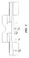
- FIG. 3is a cross sectional view of one existing example of an HBT structure having a local collector implant structure for reducing collector resistance and collector-base capacitance;
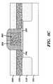
- FIG. 4is a cross sectional view of another existing example of an HBT structure having a local collector implant structure with a stepped dopant profile
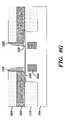
- FIG. 5is a schematic diagram illustrating various parasitic capacitance components of the HBT structures shown in FIGS. 3 and 4 ;
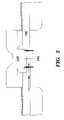
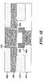
- FIG. 6is a cross sectional view of an HBT structure having a local ring shaped collector implant structure, in accordance with an embodiment of the invention.
- FIG. 7is a schematic diagram illustrating various parasitic capacitance components of the HBT structure shown in FIG. 6 ;
- FIGS. 8( a ) through 8 ( k )illustrate a sequence of exemplary process flow diagrams for forming the HBT structure shown in FIG. 6 .
- a ring shaped region of increased collector dopantis introduced beneath the perimeter region of the emitter, where the majority of collector current travels at high frequencies due to current crowding.
- the ringis self-aligned to the emitter, and as a result, collector resistance is reduced with a minimal increase in base-collector capacitance, as the increased collector doping is localized within the ring configuration at the periphery of the emitter, and not beneath the central, interior portion of the emitter (or under the extrinsic base).
- the exemplary N-type HBT structure 100includes an N++ doped, buried sub-collector region 102 formed within a substrate, and an N+ doped collector region 104 formed over the sub-collector region 102 .
- intrinsic base layer 106formed, for example, by low temperature epitaxial (LTE) growth of single crystal layer (such as SiGe) and doped with a P-type dopant (such as boron).
- Both the (P-type) raised extrinsic base structure 108 and the (N-type) emitter 110are formed from a polysilicon material, and are shown with silicide contacts 112 for providing ohmic contact to metal filled vias 114 formed within the interlevel dielectric layer (ILD) 116 .
- ILDinterlevel dielectric layer
- Also illustrated in the HBT structure 100 of FIG. 1are shallow trench isolation (STI) regions 118 (e.g., oxide), oxide layer 120 , and nitride spacers 122 .
- STIshallow trench isolation
- arrowsare shown to depict the current path from the collector through the emitter in FIG. 1 .
- FIG. 2schematically depicts the current crowding (Kirk) effect of a bipolar device, wherein the base current (horizontal arrows) encounters resistance as it travels laterally under the emitter 110 .
- the current density of the emitter(vertical arrows) is greater at the periphery of the emitter than in the center of the emitter, with the emitter-base junction bias being larger at the edge than the center of the emitter.
- one way to reduce the Kirk effect while also reducing the base-collector parasitic capacitance outside the collector current pathis to provide a localized collector implant in the collector region, self-aligned to the emitter structure.
- a localized collector implantin the collector region, self-aligned to the emitter structure.
- the collector layer 104is not provided with N+ dopant in its entirety, but rather, a local N+ type implant 302 is formed therein, corresponding to (and self-aligned with) the emitter region 110 .
- the higher doped implant region 302reduces the Kirk effect and collector resistance, while outside the collector current path, the lower doped N-type collector material keeps the collector-base capacitance in this region low.
- FIG. 4illustrates another type of collector structure for an HBT device 400 , in which the collector implant has a stepped profile, such that a lower region 402 of the implant structure has a higher dopant concentration than an upper region 404 .
- the stepped collector implant structure of FIG. 4is self-aligned to the emitter structure by dopant implantation through the emitter opening.
- the deeper implant (region 402 )links the buried collector 104 to the sub-collector 102 , providing a low resistance path to the sub-collector 102 .
- the shallow implant (region 404 )reduces the base-collector space charge region width and tailors the collector-base breakdown characteristics.
- the location/structure of the collector dopantsis still not optimized, in view of the current crowding depicted in FIG. 2 .
- the dopant of the above-described local collector implant structuresis the same within the collector current path, with respect to the cross-sectional length of the emitter structure. Accordingly, the collector-base capacitance of the interior portions of the collector current path (i.e., beneath the inner region of the emitter) is substantially the same as the exterior portions of the collector current path (i.e., beneath the perimeter of the emitter), notwithstanding the increased current density at the perimeter of emitter at high frequencies. Schematically, this is depicted in FIG. 5 .
- the local collector implant structurereduces parasitic capacitance in the extrinsic base regions (denoted by C PB ) and in the extrinsic base regions outside the collector current path (denoted by C RX )
- the parasitic capacitanceis increased in the collector current path at both the peripheral region of the emitter (denoted by C N3 ) and the inner region of the emitter (denoted by C int ).
- FIG. 6is a cross sectional view of an HBT structure 600 having a local, ring shaped collector implant structure 604 (also referred to as a ring shaped dopant profile herein) formed over a deeper collector implant 602 .
- the location of the ring shaped implant structure 604coincides with the larger current density associated with the perimeter of the emitter 110 due to current crowding.
- the dopant concentration of the ring shaped implant 604can be made lower or higher than the collector implant structure 602 , but is at least larger than the dopant concentration in collector region 104 as needed to best optimize the device performance.
- the increase in base-collector capacitance at region 606 of the collectoris minimized due to the lower collector dopant concentration therein.
- the increased collector doping of the ring structure 604reduces the collector resistance at a precisely tailored location corresponding to the bulk of the current density location, so as to delay the Kirk effect.
- the resulting improvement in parasitic base-collector capacitanceis schematically depicted in FIG. 7 .
- the component of base-collector capacitance in the collector current pathis substantially the same at both the peripheral region of the emitter (C N3 ) and the inner region of the emitter (C int ) in FIG. 5 , the absence of the increased dopant beneath the inner region of the emitter leads to an even further decreased value of C int .
- the shallow trench isolation regions 118are formed within the lightly doped collector region 104 , which has the LTE intrinsic base layer 106 grown thereon.
- the sub-collector layer beneath the collector region 104is not illustrated in FIGS. 8( a ) through 8 ( l ).
- the oxide layer 120has a sacrificial polysilicon block 802 formed thereon, which in turn is covered by a sacrificial spacer (e.g., nitride) layer 804 .
- the polysilicon block 802is dimensioned so as to correspond to the interior region of the subsequently formed emitter layer.
- the polysilicon material used for the raised extrinsic base layer 108is formed.
- a protective oxide layer 806is formed over the extrinsic base layer 108 , after which the sacrificial spacer layer 804 is removed in FIG. 8( d ). This exposes a portion of the collector layer 104 between the extrinsic base layer 108 and the sacrificial block 802 to a dopant implant step that results in the formation of the ring shaped collector implant structure 604 , as shown in FIG. 8( e ).
- the outer diameter of the ring shaped collector implant structure 604coincides with an emitter opening defined between the edges of the extrinsic base layer 108 .
- the sacrificial block 802is removed, such as by an etch process selective to polysilicon, in order to prepare the device for emitter formation.
- nitride sidewall spacers 122are formed, the etching of which also results in the etching of oxide layer 120 so as to expose the intrinsic base layer 106 .
- the lower collector implant structure 602is formed through a dopant implantation (e.g., at a dopant concentration exceeding that of collector layer 104 ).
- the lower implant structure 602is essentially aligned beneath the center portion of the subsequently formed emitter, while the ring shaped implant structure 604 is aligned beneath the periphery of the subsequently formed emitter. As such, the outer diameter of the ring shaped implant structure 604 exceeds the outer diameter of the lower implant structure.
- the polysilicon material for the emitter 110is deposited, planarized and doped with a suitable N-type dopant (e.g., phosphorous).
- a suitable N-type dopante.g., phosphorous.
- the protective oxide layer 806may be removed, down to the top of the extrinsic base layer 108 , as shown in FIG. 8( j ).
- the exposed polysilicon of the extrinsic base layer 108 and emitter 110are silicided in accordance with known techniques to form silicide contacts 112 , as also shown in FIG. 8( j ).
- the HBT structure 600is provided with an interlevel dielectric layer 116 , as shown in FIG. 8( k ), and the ILD layer 116 is patterned to form the metal filled vias 114 for connecting the terminals of the HBT device to upper wiring levels.
- the spacers 122are widened in FIG. 8( k ) to provide for a greater alignment tolerance for vias 114 . Additional information concerning spacer widening adjacent an emitter region may be found in U.S. Pat. No. 6,979,884 to Ahlgren, et al., assigned to the assignee of the present application, and the contents of which are incorporated herein by reference in their entirety. It will also be noted that additional vias (not shown) would be used to make electrical contact to the collector layer 104 as well.
- heterojunction bipolar transistorsincluding, but not limited to: AlGaAs/GaAs, InGaP/GaAs, InP/InGaAs, InAlAs/InGaAs, and InAlGaAs/InGaAs single and double heterojunction bipolar transistors with GaAs, InGaAs, InP, AlGaAs, InGaP, InAlAs, or a combination thereof as the collector material.
Landscapes
- Engineering & Computer Science (AREA)
- Physics & Mathematics (AREA)
- Condensed Matter Physics & Semiconductors (AREA)
- General Physics & Mathematics (AREA)
- Manufacturing & Machinery (AREA)
- Computer Hardware Design (AREA)
- Microelectronics & Electronic Packaging (AREA)
- Power Engineering (AREA)
- Bipolar Transistors (AREA)
Abstract
Description
Claims (5)
Priority Applications (8)
| Application Number | Priority Date | Filing Date | Title |
|---|---|---|---|
| US11/538,848US7390720B2 (en) | 2006-10-05 | 2006-10-05 | Local collector implant structure for heterojunction bipolar transistors and method of forming the same |
| JP2009530834AJP5204111B2 (en) | 2006-10-05 | 2007-09-17 | Local collector injection structure for heterojunction bipolar transistor and method of forming the same |
| CN2007800371599ACN101523579B (en) | 2006-10-05 | 2007-09-17 | Local collector implant structure for heterojunction bipolar transistors and method of forming the same |
| PCT/EP2007/059798WO2008040632A1 (en) | 2006-10-05 | 2007-09-17 | Local collector implant structure for heterojunction bipolar transistors and method of forming the same |
| KR1020097006195AKR101054701B1 (en) | 2006-10-05 | 2007-09-17 | Local collector implant structure for heterojunction bipolar transistors and method of forming the same |
| EP07820265AEP2076919B1 (en) | 2006-10-05 | 2007-09-17 | Method of forming local collector implant structure for heterojunction bipolar transistors |
| US11/870,437US7388237B2 (en) | 2006-10-05 | 2007-10-11 | Local collector implant structure for heterojunction bipolar transistors |
| US12/047,457US7473610B2 (en) | 2006-10-05 | 2008-03-13 | Local collector implant structure for heterojunction bipolar transistors and method of forming the same |
Applications Claiming Priority (1)
| Application Number | Priority Date | Filing Date | Title |
|---|---|---|---|
| US11/538,848US7390720B2 (en) | 2006-10-05 | 2006-10-05 | Local collector implant structure for heterojunction bipolar transistors and method of forming the same |
Related Child Applications (2)
| Application Number | Title | Priority Date | Filing Date |
|---|---|---|---|
| US11/870,437DivisionUS7388237B2 (en) | 2006-10-05 | 2007-10-11 | Local collector implant structure for heterojunction bipolar transistors |
| US12/047,457ContinuationUS7473610B2 (en) | 2006-10-05 | 2008-03-13 | Local collector implant structure for heterojunction bipolar transistors and method of forming the same |
Publications (2)
| Publication Number | Publication Date |
|---|---|
| US20080083934A1 US20080083934A1 (en) | 2008-04-10 |
| US7390720B2true US7390720B2 (en) | 2008-06-24 |
Family
ID=38729087
Family Applications (3)
| Application Number | Title | Priority Date | Filing Date |
|---|---|---|---|
| US11/538,848Expired - Fee RelatedUS7390720B2 (en) | 2006-10-05 | 2006-10-05 | Local collector implant structure for heterojunction bipolar transistors and method of forming the same |
| US11/870,437ActiveUS7388237B2 (en) | 2006-10-05 | 2007-10-11 | Local collector implant structure for heterojunction bipolar transistors |
| US12/047,457Expired - Fee RelatedUS7473610B2 (en) | 2006-10-05 | 2008-03-13 | Local collector implant structure for heterojunction bipolar transistors and method of forming the same |
Family Applications After (2)
| Application Number | Title | Priority Date | Filing Date |
|---|---|---|---|
| US11/870,437ActiveUS7388237B2 (en) | 2006-10-05 | 2007-10-11 | Local collector implant structure for heterojunction bipolar transistors |
| US12/047,457Expired - Fee RelatedUS7473610B2 (en) | 2006-10-05 | 2008-03-13 | Local collector implant structure for heterojunction bipolar transistors and method of forming the same |
Country Status (6)
| Country | Link |
|---|---|
| US (3) | US7390720B2 (en) |
| EP (1) | EP2076919B1 (en) |
| JP (1) | JP5204111B2 (en) |
| KR (1) | KR101054701B1 (en) |
| CN (1) | CN101523579B (en) |
| WO (1) | WO2008040632A1 (en) |
Cited By (2)
| Publication number | Priority date | Publication date | Assignee | Title |
|---|---|---|---|---|
| US20080164495A1 (en)* | 2007-01-10 | 2008-07-10 | International Business Machines Corporation | Heterojunction bipolar transistor (hbt) with self-aligned sub-lithographic metal-semiconductor alloy base contacts |
| US7868335B1 (en)* | 2008-08-18 | 2011-01-11 | Hrl Laboratories, Llc | Modulation doped super-lattice sub-collector for high-performance HBTs and BJTs |
Families Citing this family (18)
| Publication number | Priority date | Publication date | Assignee | Title |
|---|---|---|---|---|
| CN101834135A (en)* | 2010-04-22 | 2010-09-15 | 上海宏力半导体制造有限公司 | Bipolar transistor and manufacturing method thereof |
| CN101916725B (en)* | 2010-07-23 | 2015-03-18 | 上海华虹宏力半导体制造有限公司 | Method for manufacturing bipolar-junction transistor |
| JPWO2012086104A1 (en)* | 2010-12-22 | 2014-05-22 | パナソニック株式会社 | Semiconductor device |
| EP2506297A1 (en)* | 2011-03-29 | 2012-10-03 | Nxp B.V. | Bi-CMOS Device and Method |
| US20120313146A1 (en)* | 2011-06-08 | 2012-12-13 | International Business Machines Corporation | Transistor and method of forming the transistor so as to have reduced base resistance |
| CN103050517B (en)* | 2011-10-14 | 2016-06-08 | 上海华虹宏力半导体制造有限公司 | A kind of parasitic PNP device structure adopting SiGe HBT technique and preparation method thereof |
| CN103066101B (en)* | 2011-10-24 | 2016-08-17 | 上海华虹宏力半导体制造有限公司 | Germanium silicium HBT device and manufacture method |
| CN103066119B (en)* | 2011-10-24 | 2015-04-08 | 上海华虹宏力半导体制造有限公司 | Germanium silicon heterojunction bipolar transistor and manufacturing method thereof |
| CN103107188B (en)* | 2011-11-11 | 2015-08-19 | 上海华虹宏力半导体制造有限公司 | Parasitic PNP device structure in a kind of SiGe HBT technique and manufacture method thereof |
| CN102569069B (en)* | 2012-03-09 | 2014-08-27 | 中国科学院上海微系统与信息技术研究所 | SiGe-heterojunction bipolar transistor (HBT) and preparation method thereof |
| US8648391B2 (en) | 2012-03-23 | 2014-02-11 | Texas Instruments Incorporated | SiGe heterojunction bipolar transistor with an improved breakdown voltage-cutoff frequency product |
| CN103456628B (en)* | 2012-05-29 | 2015-10-14 | 上海华虹宏力半导体制造有限公司 | The manufacture method of germanium-silicon heterojunction bipolar triode device |
| CN103035685A (en)* | 2012-12-12 | 2013-04-10 | 清华大学 | Selective epitaxy outer base region bipolar transistor containing buried oxygen layer and preparation method thereof |
| CN103000680B (en)* | 2012-12-18 | 2015-06-17 | 清华大学 | Heterojunction bipolar transistor with electrode shielding structure and manufacturing method thereof |
| CN104425244B (en)* | 2013-08-20 | 2017-02-15 | 上海华虹宏力半导体制造有限公司 | Silicon-germanium heterojunction bipolar transistor manufacturing method |
| EP2996153B1 (en)* | 2014-09-12 | 2019-05-22 | Nxp B.V. | Bipolar transistor and method of manufacturing the same |
| US20160169833A1 (en)* | 2014-12-11 | 2016-06-16 | International Business Machines Corporation | Biosensor based on heterojunction bipolar transistor |
| DE102016207536B4 (en)* | 2016-05-02 | 2020-03-19 | Infineon Technologies Dresden Gmbh | Method of manufacturing a bipolar transistor |
Citations (9)
| Publication number | Priority date | Publication date | Assignee | Title |
|---|---|---|---|---|
| US5071778A (en) | 1990-06-26 | 1991-12-10 | National Semiconductor Corporation | Self-aligned collector implant for bipolar transistors |
| US5581115A (en) | 1994-10-07 | 1996-12-03 | National Semiconductor Corporation | Bipolar transistors using isolated selective doping to improve performance characteristics |
| US6440812B2 (en) | 1995-08-25 | 2002-08-27 | Micron Technology, Inc. | Angled implant to improve high current operation of bipolar transistors |
| US6506656B2 (en) | 2001-03-19 | 2003-01-14 | International Business Machines Corporation | Stepped collector implant and method for fabrication |
| US6774002B2 (en) | 2002-10-23 | 2004-08-10 | United Microelectronics Corp. | Structure and method for forming self-aligned bipolar junction transistor with expitaxy base |
| US20040188712A1 (en) | 2002-10-08 | 2004-09-30 | Eic Corporation | Heterojunction bipolar transistor having non-uniformly doped collector for improved safe-operating area |
| US6979884B2 (en) | 2003-12-04 | 2005-12-27 | International Business Machines Corporation | Bipolar transistor having self-aligned silicide and a self-aligned emitter contact border |
| US7075126B2 (en) | 2004-02-27 | 2006-07-11 | International Business Machines Corporation | Transistor structure with minimized parasitics and method of fabricating the same |
| US7151035B2 (en)* | 2002-04-16 | 2006-12-19 | Renesas Technology Corp. | Semiconductor device and manufacturing method thereof |
Family Cites Families (9)
| Publication number | Priority date | Publication date | Assignee | Title |
|---|---|---|---|---|
| JPH0348427A (en)* | 1989-04-04 | 1991-03-01 | Matsushita Electric Ind Co Ltd | Bipolar semiconductor device and its manufacturing method |
| US5183768A (en)* | 1989-04-04 | 1993-02-02 | Matsushita Electric Industrial Co., Ltd. | Method of fabricating semiconductor device by forming doped regions that limit width of the base |
| JPH053202A (en)* | 1991-06-26 | 1993-01-08 | Fujitsu Ltd | Semiconductor device and manufacturing method thereof |
| JPH05243243A (en)* | 1992-02-28 | 1993-09-21 | Toshiba Corp | Semiconductor device and manufacture thereof |
| JPH10294320A (en)* | 1997-04-18 | 1998-11-04 | Nec Corp | Semiconductor device and manufacturing method thereof |
| US6441462B1 (en)* | 2001-07-10 | 2002-08-27 | International Business Machines Corporation | Self-aligned SiGe NPN with improved ESD robustness using wide emitter polysilicon extension |
| US7064415B1 (en)* | 2002-08-13 | 2006-06-20 | Newport Fab Llc | Self-aligned bipolar transistor having increased manufacturability |
| WO2005114738A1 (en) | 2004-04-22 | 2005-12-01 | International Business Machines Corporation | Tuneable semiconductor device |
| US7297992B1 (en)* | 2004-11-23 | 2007-11-20 | Newport Fab, Llc | Method and structure for integration of phosphorous emitter in an NPN device in a BiCMOS process |
- 2006
- 2006-10-05USUS11/538,848patent/US7390720B2/ennot_activeExpired - Fee Related
- 2007
- 2007-09-17CNCN2007800371599Apatent/CN101523579B/enactiveActive
- 2007-09-17KRKR1020097006195Apatent/KR101054701B1/ennot_activeExpired - Fee Related
- 2007-09-17WOPCT/EP2007/059798patent/WO2008040632A1/enactiveApplication Filing
- 2007-09-17EPEP07820265Apatent/EP2076919B1/ennot_activeNot-in-force
- 2007-09-17JPJP2009530834Apatent/JP5204111B2/ennot_activeExpired - Fee Related
- 2007-10-11USUS11/870,437patent/US7388237B2/enactiveActive
- 2008
- 2008-03-13USUS12/047,457patent/US7473610B2/ennot_activeExpired - Fee Related
Patent Citations (10)
| Publication number | Priority date | Publication date | Assignee | Title |
|---|---|---|---|---|
| US5071778A (en) | 1990-06-26 | 1991-12-10 | National Semiconductor Corporation | Self-aligned collector implant for bipolar transistors |
| US5581115A (en) | 1994-10-07 | 1996-12-03 | National Semiconductor Corporation | Bipolar transistors using isolated selective doping to improve performance characteristics |
| US5698459A (en) | 1994-10-07 | 1997-12-16 | National Semiconductor Corporation | Fabrication of bipolar transistors using selective doping to improve performance characteristics |
| US6440812B2 (en) | 1995-08-25 | 2002-08-27 | Micron Technology, Inc. | Angled implant to improve high current operation of bipolar transistors |
| US6506656B2 (en) | 2001-03-19 | 2003-01-14 | International Business Machines Corporation | Stepped collector implant and method for fabrication |
| US7151035B2 (en)* | 2002-04-16 | 2006-12-19 | Renesas Technology Corp. | Semiconductor device and manufacturing method thereof |
| US20040188712A1 (en) | 2002-10-08 | 2004-09-30 | Eic Corporation | Heterojunction bipolar transistor having non-uniformly doped collector for improved safe-operating area |
| US6774002B2 (en) | 2002-10-23 | 2004-08-10 | United Microelectronics Corp. | Structure and method for forming self-aligned bipolar junction transistor with expitaxy base |
| US6979884B2 (en) | 2003-12-04 | 2005-12-27 | International Business Machines Corporation | Bipolar transistor having self-aligned silicide and a self-aligned emitter contact border |
| US7075126B2 (en) | 2004-02-27 | 2006-07-11 | International Business Machines Corporation | Transistor structure with minimized parasitics and method of fabricating the same |
Non-Patent Citations (1)
| Title |
|---|
| Khater, M., et al, "SiGe HBT Technology with Fmax/fT=350/300 GHz and Gate Delay Below 3.3 ps". |
Cited By (3)
| Publication number | Priority date | Publication date | Assignee | Title |
|---|---|---|---|---|
| US20080164495A1 (en)* | 2007-01-10 | 2008-07-10 | International Business Machines Corporation | Heterojunction bipolar transistor (hbt) with self-aligned sub-lithographic metal-semiconductor alloy base contacts |
| US7952165B2 (en)* | 2007-01-10 | 2011-05-31 | International Business Machines Corporation | Heterojunction bipolar transistor (HBT) with self-aligned sub-lithographic metal-semiconductor alloy base contacts |
| US7868335B1 (en)* | 2008-08-18 | 2011-01-11 | Hrl Laboratories, Llc | Modulation doped super-lattice sub-collector for high-performance HBTs and BJTs |
Also Published As
| Publication number | Publication date |
|---|---|
| EP2076919A1 (en) | 2009-07-08 |
| US20080083934A1 (en) | 2008-04-10 |
| KR20090067144A (en) | 2009-06-24 |
| US7388237B2 (en) | 2008-06-17 |
| US20080166850A1 (en) | 2008-07-10 |
| US7473610B2 (en) | 2009-01-06 |
| CN101523579B (en) | 2012-06-27 |
| US20080083935A1 (en) | 2008-04-10 |
| WO2008040632A1 (en) | 2008-04-10 |
| JP5204111B2 (en) | 2013-06-05 |
| JP2010506390A (en) | 2010-02-25 |
| CN101523579A (en) | 2009-09-02 |
| EP2076919B1 (en) | 2012-08-29 |
| KR101054701B1 (en) | 2011-08-08 |
Similar Documents
| Publication | Publication Date | Title |
|---|---|---|
| US7390720B2 (en) | Local collector implant structure for heterojunction bipolar transistors and method of forming the same | |
| US7932541B2 (en) | High performance collector-up bipolar transistor | |
| JP3701873B2 (en) | Heterojunction Bipolar Transistor Fabrication Method | |
| JP3494638B2 (en) | Semiconductor device and method of manufacturing semiconductor device | |
| US7442595B2 (en) | Bipolar transistor with collector having an epitaxial Si:C region | |
| US10014397B1 (en) | Bipolar junction transistors with a combined vertical-lateral architecture | |
| EP3843159A1 (en) | Semiconductor device with a base link region and method therefor | |
| US11721726B2 (en) | Horizontal current bipolar transistor with silicon-germanium base | |
| US20120037914A1 (en) | Heterojunction biopolar transistor and manufacturing method | |
| KR20030047274A (en) | a Super self-aligned heterojunction bipolar device and a method for fabricating the same | |
| US6586818B1 (en) | Self-aligned silicon germanium heterojunction bipolar transistor device with electrostatic discharge crevice cover for salicide displacement | |
| US8759880B2 (en) | Ultra-high voltage SIGE HBT device and manufacturing method of the same | |
| JP3953344B2 (en) | Stepped collector implant and method for forming the same | |
| US7008851B2 (en) | Silicon-germanium mesa transistor | |
| US6847063B2 (en) | Semiconductor device | |
| US20250254900A1 (en) | Semiconductor device with monocrystalline extrinsic base | |
| US11901414B2 (en) | Semiconductor device with a defect layer and method of fabrication therefor | |
| US20250081486A1 (en) | Utilization of sacrificial material for current electrode formation | |
| US20240204052A1 (en) | Semiconductor device with lateral base link region | |
| Iinuma et al. | Sub-20 ps high-speed ECL bipolar transistor with low parasitic architecture |
Legal Events
| Date | Code | Title | Description |
|---|---|---|---|
| AS | Assignment | Owner name:INTERNATIONAL BUSINESS MACHINES CORPORATION, NEW Y Free format text:ASSIGNMENT OF ASSIGNORS INTEREST;ASSIGNOR:PAGETTE, FRANCOIS;REEL/FRAME:018671/0810 Effective date:20060920 | |
| FEPP | Fee payment procedure | Free format text:PAYOR NUMBER ASSIGNED (ORIGINAL EVENT CODE: ASPN); ENTITY STATUS OF PATENT OWNER: LARGE ENTITY | |
| STCF | Information on status: patent grant | Free format text:PATENTED CASE | |
| FPAY | Fee payment | Year of fee payment:4 | |
| AS | Assignment | Owner name:GLOBALFOUNDRIES U.S. 2 LLC, NEW YORK Free format text:ASSIGNMENT OF ASSIGNORS INTEREST;ASSIGNOR:INTERNATIONAL BUSINESS MACHINES CORPORATION;REEL/FRAME:036550/0001 Effective date:20150629 | |
| AS | Assignment | Owner name:GLOBALFOUNDRIES INC., CAYMAN ISLANDS Free format text:ASSIGNMENT OF ASSIGNORS INTEREST;ASSIGNORS:GLOBALFOUNDRIES U.S. 2 LLC;GLOBALFOUNDRIES U.S. INC.;REEL/FRAME:036779/0001 Effective date:20150910 | |
| FPAY | Fee payment | Year of fee payment:8 | |
| AS | Assignment | Owner name:WILMINGTON TRUST, NATIONAL ASSOCIATION, DELAWARE Free format text:SECURITY AGREEMENT;ASSIGNOR:GLOBALFOUNDRIES INC.;REEL/FRAME:049490/0001 Effective date:20181127 | |
| FEPP | Fee payment procedure | Free format text:MAINTENANCE FEE REMINDER MAILED (ORIGINAL EVENT CODE: REM.); ENTITY STATUS OF PATENT OWNER: LARGE ENTITY | |
| LAPS | Lapse for failure to pay maintenance fees | Free format text:PATENT EXPIRED FOR FAILURE TO PAY MAINTENANCE FEES (ORIGINAL EVENT CODE: EXP.); ENTITY STATUS OF PATENT OWNER: LARGE ENTITY | |
| STCH | Information on status: patent discontinuation | Free format text:PATENT EXPIRED DUE TO NONPAYMENT OF MAINTENANCE FEES UNDER 37 CFR 1.362 | |
| FP | Lapsed due to failure to pay maintenance fee | Effective date:20200624 | |
| AS | Assignment | Owner name:GLOBALFOUNDRIES INC., CAYMAN ISLANDS Free format text:RELEASE BY SECURED PARTY;ASSIGNOR:WILMINGTON TRUST, NATIONAL ASSOCIATION;REEL/FRAME:054636/0001 Effective date:20201117 | |
| AS | Assignment | Owner name:GLOBALFOUNDRIES U.S. INC., NEW YORK Free format text:RELEASE BY SECURED PARTY;ASSIGNOR:WILMINGTON TRUST, NATIONAL ASSOCIATION;REEL/FRAME:056987/0001 Effective date:20201117 |